

Page 1

ORDER NO.
RRV2608
DVD RECORDER
DVR-7000
THIS MANUAL IS APPLICABLE TO THE FOLLOWING MODEL(S) AND TYPE(S).
Type
WL/RD AC220–240V 4
This service manual should be used together with the following manual(s):
Model
DVR-7000
Power Requirement Region No. Remarks
Model
DVR-7000/KU/CA
DVR-A03/KB
For details, refer to "Important symbols for good services" on page 4.
RRV2536 DVD Recorder
RRV2423 DVD-R/RW Drive Unit
RemarksOrder No.
PIONEER CORPORATION 4-1, Meguro 1-chome, Meguro-ku, Tokyo 153-8654, Japan
PIONEER ELECTRONICS (USA) INC. P.O. Box 1760, Long Beach, CA 90801-1760, U.S.A.
PIONEER EUROPE NV Haven 1087, Keetberglaan 1, 9120 Melsele, Belgium
PIONEER ELECTRONICS ASIACENTRE PTE. LTD. 253 Alexandra Road, #04-01, Singapore 159936
PIONEER CORPORATION 2002
T – ZZV APR. 2002 Printed in Japan
Page 2
DVR-7000
SAFETY INFORMATION
This service manual is intended for qualified service technicians; it is not meant for the casual
do-it-yourselfer. Qualified technicians have the necessary test equipment and tools, and have been
trained to properly and safely repair complex products such as those covered by this manual.
Improperly performed repairs can adversely affect the safety and reliability of the product and may
void the warranty . If you are not qualified to perform the repair of this product properly and safely, you
should not risk trying to do so and refer the repair to a qualified service technician.
WARNING
This product contains lead in solder and certain electrical parts contain chemicals which are known to the state of California to
cause cancer, birth defects or other reproductive harm.
Health & Safety Code Section 25249.6 – Proposition 65
NOTICE
(FOR CANADIAN MODEL ONLY)
Fuse symbols (fast operating fuse) and/or (slow operating fuse) on PCB indicate that replacement
parts must be of identical designation.
REMARQUE
(POUR MODÈLE CANADIEN SEULEMENT)
Les symboles de fusible (fusible de type rapide) et/ou (fusible de type lent) sur CCI indiquent que
les pièces de remplacement doivent avoir la même désignation.
(FOR USA MODEL ONLY)
1. SAFETY PRECAUTIONS
The following check should be performed for the
continued protection of the customer and service
technician.
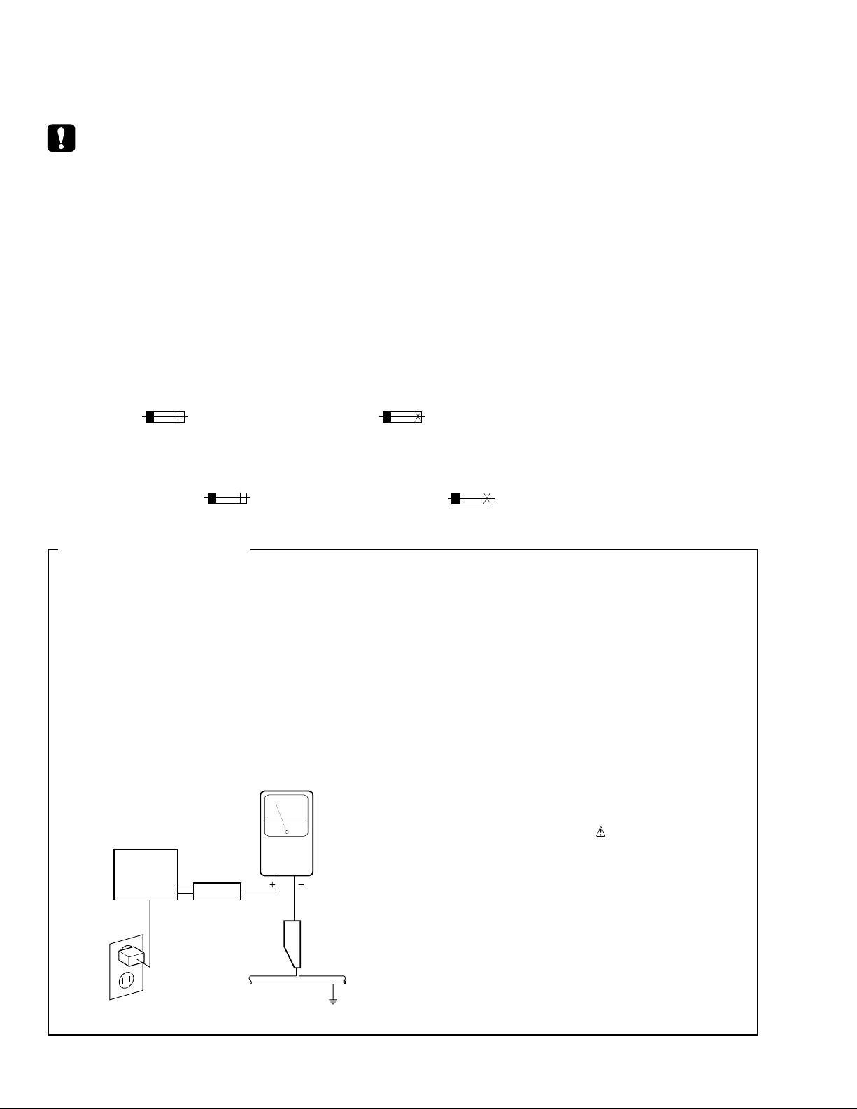
LEAKAGE CURRENT CHECK
Measure leakage current to a known earth ground
(water pipe, conduit, etc.) by connecting a leakage
current tester such as Simpson Model 229-2 or
equivalent between the earth ground and all exposed
metal parts of the appliance (input/output terminals,
screwheads, metal overlays, control shaft, etc.). Plug
the AC line cord of the appliance directly into a 120V
AC 60 Hz outlet and turn the AC power switch on. Any
current measured must not exceed 0.5 mA.
Reading should
not be above
0.5 mA
Earth
ground
Device
under
test
Also test with
plug reversed
(Using AC adapter
plug as required)
Test all
exposed metal
surfaces
AC Leakage Test
Leakage
current
tester
ANY MEASUREMENTS NOT WITHIN THE
LIMITS OUTLINED ABOVE ARE INDICATIVE
OF A POTENTIAL SHOCK HAZARD AND
MUST BE CORRECTED BEFORE RETURNING THE APPLIANCE TO THE CUSTOMER.
2. PRODUCT SAFETY NOTICE
Many electrical and mechanical parts in the appliance
have special safety related characteristics. These are
often not evident from visual inspection nor the
protection afforded by them necessarily can be obtained
by using replacement components rated for voltage,
wattage, etc. Replacement parts which have these
special safety characteristics are identified in this
Service Manual.
Electrical components having such features are
identified by marking with a
on the parts list in this Service Manual.
The use of a substitute replacement component which
does not have the same safety characteristics as the
PIONEER recommended replacement one, shown in the
parts list in this Service Manual, may create shock, fire,
or other hazards.
Product Safety is continuously under review and new
instructions are issued from time to time. For the latest
information, always consult the current PIONEER
Service Manual. A subscription to, or additional copies
of, PIONEER Service Manual may be obtained at a
nominal charge from PIONEER.
on the schematics and
2
Page 3
IMPORTANT
THIS PIONNER APPARATUS CONTAINS
LASER OF CLASS 1.
SERVICING OPERATION OF THE APPARATUS
SHOULD BE DONE BY A SPECIALLY
INSTRUCTED PERSON.
LASER DIODE CHARACTERISTICS
MAXIMUM OUTPUT POWER : 35 mW
WAVELENGTH : 658 nm
LABEL CHECK
WARNING!
DEVICE INCLUDES LASER DIODE WHICH
EMITS INVISIBLE INFRARED RADIATION
WHICH IS DANGEROUS TO EYES. THERE IS
A WARNING SIGN ACCORDING TO PICTURE
1 INSIDE THE DEVICE CLOSE TO THE LASER
DIODE.
DVR-7000
LASER
Picture 1
Warning sign for
laser radiation
Printed on Rear Panel
1. The ON/OFF(ON:low level,OFF:high level) status of the
CLAMP signals for detecting the loading state are detected
by the drive CPUs, and the design prevents laser diode
oscillation when the CLAMP signal turns OFF.
In normal operation, if no disc is clamped, the laser diode
oscillation is disabled.
However, the interlock does not always operate in the test
mode.
*
VRW1914
Additional Laser Caution
2. When the cover is opened, close viewing of the objective
lens with the naked eye will cause exposure to a Class 3A
laser beam.
* Refer to pages 43 of DVR-A03 Service Manual(RRV2423).
3
Page 4
DVR-7000
[ Important symbols for good services ]
In this manual, the symbols shown-below indicate that adjustments, settings or cleaning should be made securely.
When you find the procedures bearing any of the symbols, be sure to fulfill them:
1. Product safety
You should conform to the regulations governing the product (safety, radio and noise, and other regulations), and
should keep the safety during servicing by following the safety instructions described in this manual.
2. Adjustments
To keep the original performances of the product, optimum adjustments or specification confirmation is indispensable.
In accordance with the procedures or instructions described in this manual, adjustments should be performed.
3. Cleaning
For optical pickups, tape-deck heads, lenses and mirrors used in projection monitors, and other parts requiring cleaning,
proper cleaning should be performed to restore their performances.
4. Shipping mode and shipping screws
To protect the product from damages or failures that may be caused during transit, the shipping mode should be set or
the shipping screws should be installed before shipping out in accordance with this manual, if necessary.
5. Lubricants, glues, and replacement parts
Appropriately applying grease or glue can maintain the product performances. But improper lubrication or applying
glue may lead to failures or troubles in the product. By following the instructions in this manual, be sure to apply the
prescribed grease or glue to proper portions by the appropriate amount.For replacement parts or tools, the prescribed
ones should be used.
4
Page 5

CONTENTS
SAFETY INFORMATION
1. CONTRAST OF MISCHELLANEOUS PARTS
2. BLOCKDIAGRAM AND SCHEMATIC DIAGRAM
2.1
2.2
2.3
2.4
2.5
2.6
2.7
2.8
2.9
2.10
3. PCB CONNECTION DIAGRAM
3.1
3.2
4. ADJUSTMENT
4.1
4.2
5. GENERAL INFORMATION
5.1
5.2 IC
6. PANEL FACILITIES AND SPECIFICATIONS
BLOCKDIAGRAM
OVERALL WIRING DIAGRAM
TUMJ ASSY(1/4) and REAR JACK ASSY
TUMJ ASSY(2/4)
TUMJ ASSY(3/4) and SECAM ASSY
TUMJ ASSY(4/4) and FRONT JACK ASSY
MAIN ASSY(4/10)
MAIN ASSY(7/10)
MAIN ASSY(8/10)
MAIN ASSY(10/10)
TUMJ ASSY
REAR JACK, SECAM and FRONT JACK ASSYS
......................................................
TUMJ ASSY ADJUSTMENT
MAIN ASSY ADJUSTMENT
MODEL TYPE AND REGION SETTING
...................................................................
............................................
..............................................
..........................
........
...............................................
................
..............................................
..............................................
..............................................
..........................................
............................
.......................................................
..............................
..............................
..................................
...........
.......
...
......
....
......
DVR-7000
2
6
14
14
20
22
24
26
28
30
32
34
36
38
38
42
44
44
45
47
47
48
57
5
Page 6
DVR-7000
1. CONTRAST OF MISCELLANEOUS PARTS
NOTES:
CONTRAST TABLE
DVR-7000/WL/RD and /KU/CA types are constructed the same except for the following:
Ref.
No.
P7-1 TUMJ ASSY VWV1885 VWV1897
P7-2 REAR JACK ASSY VWV1887 VWV1883
P7-3 SECAM ASSY Not used VWV1892
P7-3 3D Y/C ASSY VWV1888 Not used
Parts marked by "NSP" are generally unavailable because they are not in our Master Spare Parts List.
The mark found on some component parts indicates the importance of the safety factor of the part.
Therefore, when replacing, be sure to use parts of identical designation.
Screws adjacent to mark on product are used for disassembly.
Reference Nos. indicate the pages and Nos. in the service manual for the base model.
When ordering resistors, first convert resistance values into code form as shown in the following examples.
Ex.1 When there are 2 effective digits (any digit apart from 0), such as 560 ohm and 47k ohm (tolerance is shown by J=5%,
and K=10%).
560
47k
0.5
1
56 x 10
47 x 103
R50
1R0
1
561
473
RD1/4PU J
RD1/4PU J
RN2H K
RS1P K
561
473
R50
1R0
Ex.2 When there are 3 effective digits (such as in high precision metal film resistors).
5.62k RN1/4PC F562 x 10
1
5621
5621
Part No.
Mark Symbol and Description
DVR-7000/KU/CA DVR-7000/WL/RD
PCB ASSEMBLIES
TUJB ASSY VWM2103 VWM2112
Remarks
P7-4 FRONT JACK ASSY VWV1886 VWV1890
P7-5 MAIN ASSY VWV1894 VWV1895
P7-6 POWER SUPPLY ASSY VWR1347 VWR1348
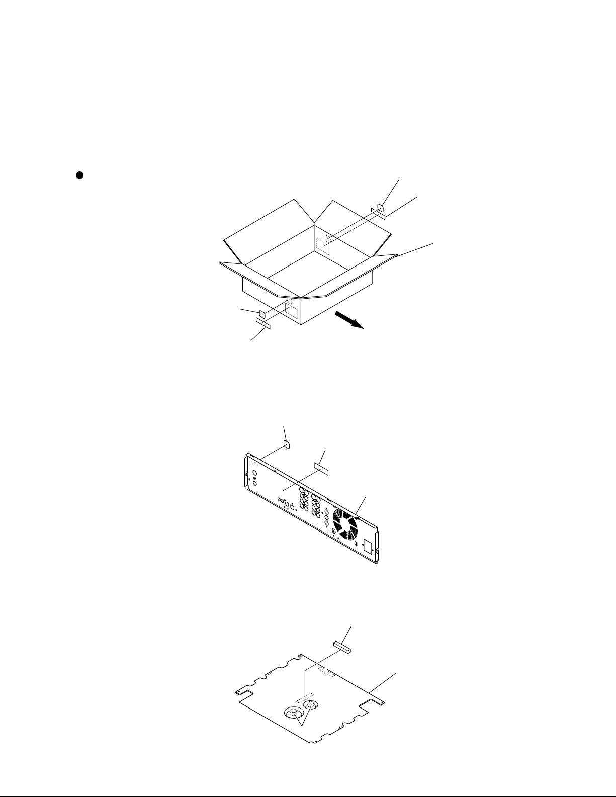
PACKING SECTION
P5-1 RF Antenna Cable VDE1025 Not used
P5-1 RF Antenna Cable (PAL) Not used VDE1075
P5-4 AC Power Code ADG7021 ADG1127
AC Power Code (T5A fuse inside) Not used ADG1156
P5-6 NSP Warranty Card ARY1026 Not used
P5-7 Operating Instructions (English) VRB1275 VRB1283
P5-8 Operating Instructions (Chinese) Not used VRE1097
P5-9 Remote Control Unit VXX2763 VXX2777
P5-11 NSP DVD-RW Disc Ver.1.1 VZZ1001 Not used
WL/RD Label Not used VRW1933 No.1
Region Label P4 Not used VRW1705 No.2
P5-15 Packing Case VHG2122 VHG2175
EXTERIOR SECTION
P7-13 Housing Assy (10P) VKP2264 VKP2276 MAIN CN8001-TUMJ CN3001
P7-33 Rear Panel VNA2328 VNA2408
P7-33 NSP Upper Plate Assy VNE2272 Not used
NSP Upper Plate Not used VNE2246 No.3
P7-62 Cooling Sheet S VEB1333 Not used
P7-69 65 Label ARW7050 Not used
P7-70 Fuse Caution Label VRW1902 Not used
P7-71 Fuse Caution Label VRW1903 Not used
Region Label R4 Not used VRW1704 No.4
C-Tic Label Not used VRW1932 No.5
FRONT PANEL SECTION
P9-7 Front Aluminium VAH1392 VAH1378
P9-17 Panel Base VNK4983 VNK4799
P9-18 Input Door VNK4924 VNK4800
6
Page 7
DVR-7000
Notes: ÷ The numbers in the remarks column correspond to the numbers on "EXPLOEDED VIEWS".
÷ For ASSEMBLIES, refer to “CONTRAST OF PCB ASSEMBLIES”,“PCB PARTS LIST” and “3. BLOCK DIAGRAM AND SCHE-
MATIC DIAGRAM”.
EXPLODED VIEWS
No.2
(Region Label P4)
No.1
(WL/RD Label)
No.4
(Region Label R4)
No.2
(Region Label P4)
No.1
(WL/RD Label)
Packing Case
Front Side
No.5
(C-Tic Label)
Removed
Rear Panel
VEC2253
(Gasket(M))
Attaching place is changed.
No.3
(Upper Plate)
7
Page 8
DVR-7000
CONTRAST OF PCB ASSEMBLIES
E
MAIN ASSY
VWV1895 and VWV1894 are constructed the same except for the following:
Mark Symbol and Description
VWV1894 VWV1895
IC1008 (FLASH ROM) VYW1970 VYW1972
IC4002 (SDRAM 16M) Not used
IC5003,IC5004 (SDRAM 64M) TC59S6432CFT-80 W986432DH-7
IC7004 (SGRAM 16M) M32L1632512A-8Q Not used
IC7006 (Video Encoder) PM0024AF Not used
Part No.
MB81F161622C-80FN
Remarks
∗1
IC9502 (Stream Check)
IC9503 (EPLD) PDY078A PDY076A
Q7001,Q7002 Not used 2SA1576A ∗2
Q7006,Q7008 2SA1576A Not used
L3018 VTL1079 Not used
L7003,L7004,L7008-L7010 VTL1124 Not used
F0863 Not used VTF1096 ∗3
F8008 VTF1096 Not used
C1018 CEV221M4 VCH1234
C4012,C4014,C4027,C4029,C4035 Not used CKSRYF104Z25 ∗1
C7001,C7002 Not used CKSRYF105Z10 ∗2
C7095 CEV100M16 Not used
C7051 CEV101M16 Not used
C7003-C7005,C7058,C7065,C7101,C7104
C7096,C7097,C9501-C9506,C9512-C9515
C7006-C7009,C7044,C7059-C7064 CKSRYF105Z10 Not used
C7070,C7071,C7082,C7083,C7089,C7090
C7099,C7102,C7103,C7108-C7111 CKSRYF105Z10 Not used
C7010,C7027,C7028,C7042,C7043,C7056
C7100 CKSQYF475Z10 Not used
C0826 Not used CCSRCH221J50 ∗3
C8111 CEV101M6R3 VCH1235
C8121,8126 CEV101M16 VCH1235
C8123,C8131 CCSRCH750J50 CCSRCH560J50
C8124,C8129 CCSRCH471J50 CCSRCH221J50
UPD65954GC-E59-7EA
CEV221M4 Not used
CKSRYF104Z25 Not used
CKSRYF105Z10 Not used
CKSQYF225Z16 Not used
Not used
C8089,C8094,C8107,C8108,C8127 CKSRYF104Z25 CKSRYF105Z10
R3102 RS1/16S101J Not used
R7072 RS1/16S470J RS1/16S330J
R7025 RS1/16S103J RS1/16S331J
R7001-R7003,R7007-R7009,R7016-R7018
R7100,R7129 Not used RS1/16S0R0J
R7010-R7015 Not used RS1/16S220J ∗2
R7205,R7206 Not used RS1/16S101J
R7004,R7005 Not used RS1/16S222J
R7110 RS1/16S3300F Not used
R7081,R7089,R7115,R7119 RAB4C0R0J Not used
R7042-R7044,R7067,R7068,R7084 RAB4C220J Not used
R7006,R7019,R7037,R7041,R7046,R7047
R7051-R7054,R7066,R7069,R7070,R7106
R7107,R7114,R7116-R7118,R7121,R7122
Not used RAB4C0R0J
RS1/16S0R0J Not used
RS1/16S0R0J Not used
RS1/16S0R0J Not used
8
Page 9
DVR-7000
Mark Symbol and Description
R7099 RS1/10S220J Not used
R7036,R7045,R7095-R7098,R7101,R7130
R7127,R7128 RS1/16S101J Not used
R7090 RS1/16S332J Not used
R7120 RS1/16S103J Not used
R8074,R8116 RS1/16S5600F RS1/16S8200F
R8018,R8020,R8021 RS1/16S0R0J RS1/16S471J
R0808 Not used RS1/10S0R0J
R8063 RS1/10S0R0J Not used
R8139,R8140,R8301,R8302 RS1/16S221J Not used
R9503,R9506,R9515 Not used RAB4C220J ∗4
R9509-R9512,R9517,R9520,R9528 RAB4C220J Not used
R9529,R9540,R9541 RAB4C220J Not used
R9508,R9576 RS1/16S0R0J Not used
R9538,R9539,R9701,R9702 RS1/16S220J Not used
R9516 RS1/16S103J Not used
VR7001,VR7002 (100Ω) Not used VCP1167
VR7006,VR7007 (470Ω) VCP1169 Not used
VWV1894 VWV1895
RS1/16S220J Not used
Part No.
*1 Refer to " 3. BLOCK DIAGRAM AND SCHEMATIC DIAGRAM" page 30.
*2 Refer to " 3. BLOCK DIAGRAM AND SCHEMATIC DIAGRAM" page 33.
*3 Refer to " 3. BLOCK DIAGRAM AND SCHEMATIC DIAGRAM" page 34.
*4 Refer to " 3. BLOCK DIAGRAM AND SCHEMATIC DIAGRAM" page 36.
Remarks
∗3
∗2
I
POWER SUPPLY ASSY
VWR1348 and VWR1347 are constructed the same except for the following:
Mark Symbol and Description
VWR1347 VWR1348
Q110 VZF1108 VZF1096
(2SK2750) (2SK2700)
Q120 VZF1101 VZF1095
(2SK2543) (2SK2717)
Q412 VZF1113 VZF1122
(2SA954L) (2SA1315)
D110 VZF1105 VZF1123
(HZS2C3) (HZS3B3)
D103 UK1V26 Not used
FU101 VEK1044 AEK1059
(3.15A) (T3.15A)
Notes: ÷ The upper contrast table is restricted to the service parts.
Part No.
Remarks
9
Page 10

DVR-7000
PCB PARTS LIST
Mark No. Description Part No.
A
TUMJ ASSY
SEMICONDUCTORS
IC2002 BA033FP
IC2011 PQ12RF11
Q1831, Q2004 2SD1664
Q3431, Q4301 2SD1664
IC2013 BA10393F
IC4402 BA4558F–HT
IC1102 BA7046F
IC1351 BA7665FS
IC2010, IC5501 BR24E16FV
IC4201 BU4052BCFV
IC7001 LC74793JM
IC1002 MM1114XF
IC1003, IC1004, IC1171 MM1118XF
IC4702 MSP3417G
IC2003 PE5322D9
IC2017 PST9120N
IC2007 PST9130N
IC2008 RV5C386A
IC1421, IC2001, IC2012, IC7003 SN74AHC1G08HDCK
IC2006 SN74AHC2G126HDCT
IC2004 SN74AHC2GU04HDCT
IC1001, IC1103 SN74LV4052APW
IC2009, IC3222 TC4W53FU
IC1101 TC74HC123AF
IC2005, IC2301 TC74VHCT541AFT
IC4701, IC7002 TC7SET08FU
IC4101, IC7006 TK15404M
IC1901, IC1902, IC3241 TK15420M
IC1312 TK15453V
IC4202, IC4302 UPC4570G2
Q1103, Q1106, Q1203, Q1207 2SA1576A
Q1211 2SA1576A
Q3211, Q4308 2SA1576A
Q2006, Q4411, Q4413 2SB1132
Q2002 2SB1237X
Q1311, Q1411, Q2023, Q2203 2SC4081
Q3221, Q3222, Q4102, Q4108 2SC4081
Q4161, Q4162 2SC4081
Q2007 2SD1664
Q4401, Q4406 2SD1664
Q2009, Q2010, Q2022, Q4345 2SD2114K
Q4355 2SD2114K
Q1104 2SK210
Q1108, Q2001, Q2021 DTA124EUA
Q1172, Q1341, Q2013, Q2024 DTC124EUA
Q3223,Q7002 DTC124EUA
Q2003, Q2005, Q4412, Q4414 DTC143EUA
Q1101, Q1113, Q1223, Q1224 HN1A01FU
Q1227, Q1228, Q1231, Q1232 HN1A01FU
Q3212,Q4304,Q4305 HN1A01FU
Q4103, Q4104 HN1B01FU
Q1114, Q1115, Q2202 HN1C01FU
Q2008, Q2012, Q2015, Q2016 HN1K03FU
Q4107,Q4601, Q7001 HN1K03FU
Q4201 RN1903
Q2014 RN2903
Mark No. Description Part No.
D1051, D1956, D2001 EP10QY03
Q2002,D2073, D2074 EP10QY03
D1101, D1103, D1401 MA111
D2021–D2023, D2041 MA111
D2201,D4302, D4501 MA111
D4101 UDZ33B
D4301 UDZS8.2B
D4601, D4602 UDZS6.8B
D4725–D4727 UDZS6.8B
COILS AND FILTERS
L1401, L1412 LCTA100J2520
L4111, L7031 LCTA470J2520
L4161 LCYA150J2520
L4162 LCYA220J2520
L4163 LCYA330J2520
L4164 LCYA3R3J2520
F1202, F1204, F1206, F3241, F3242 VTF1166
F1821, F2007–F2009, F4701–F4703 VTF1170
F7001, F7002 VTF1170
L4152, L4153 VTL1075
L4101, L4102, L7003 VTL1096
CAPACITORS
C1120, C2043 CCSRCH100D50
C1336, C1337, C2029, C2030 CCSRCH101J50
C4150, C4151 CCSRCH101J50
C1003, C1010, C1035, C1115, C4325 CCSRCH102J50
C4334 CCSRCH102J50
C4161, C4163, C4202, C4216, C4303 CCSRCH220J50
C4333 CCSRCH220J50
C1113, C2202, C2203, C4164 CCSRCH221J50
C4502 CCSRCH470J50
C4162, C4718, C4719 CCSRCH560J50
C4152, C7031 CCSRCH680J50
C4721, C4722 CCSRCJ3R0C50
C1351 CEANP2R2M50
C2015, C4108, C4111, C4118 CEAT100M50
C4205–C4207, C4221–C4223, C4320 CEAT100M50
C4331, C4705, C4712 CEAT100M50
C1001, C1014, C1024, C1112 CEAT101M10
C1117, C1118, C1175, C1201, C1204 CEAT101M10
C1207, C1317, C1354, C1401, C1402 CEAT101M10
C1821, C1831, C1834, C2009 CEAT101M10
C2018–C2020, C2022, C2025, C2032 CEAT101M10
C2035, C2041, C2049, C2054 CEAT101M10
C2057, C2058, C2060, C2062, C2072 CEAT101M10
C2302, C3431, C3434, C4103, C4106 CEAT101M10
C4115, C4116, C4120, C4348, C4410 CEAT101M10
C4412, C4414, C4416, C4432, C4701 CEAT101M10
C4711, C4720, C5501, C7001, C7011 CEAT101M10
C1007, C1101, C1103, C1106 CEAT101M16
C1804, C1811, C1812, C1901, C1903 CEAT101M16
C2006, C2007, C3211, C3227, C3235 CEAT101M16
C3241, C4301, C4305, C4307, C4310 CEAT101M16
C4403, C4431, C4433 CEAT101M16
C2004, C2027 CEAT101M25
C1320 CEAT102M6R3
C1005, C1009, C1012, C1013 CEAT1R0M50
10
Page 11

DVR-7000
Mark No. Description Part No.
C1032, C1033, C1171, C7005, C7006 CEAT1R0M50
C1356, C1358 CEAT220M25
C1414 CEAT221M6R3
C4706 CEAT3R3M50
C1054, C1057, C1415 CEAT470M16
C2067 CEAT471M16
C1058, C1322, C1324, C1355, C1357 CEAT471M6R3
C1832, C3432 CEAT471M6R3
C7007 CEAT4R7M50
C2039 CEHAZA221M6R3
C1127, C4105, C4107, C4114, C4121 CKSRYB102K50
C4344, C4345 CKSRYB102K50
C1006, C1016, C1023, C1176, C1412 CKSRYB103K50
C2016, C2091, C3225, C3228, C4110 CKSRYB103K50
C4117, C4169, C4319, C4330 CKSRYB103K50
C1004, C1011, C1034, C1105, C1318 CKSRYB104K16
C1352, C1359, C3224, C3246 CKSRYB104K16
C1319, C1323 CKSRYB105K6R3
C4318, C4329 CKSRYB472K50
C4347, C4357 CKSRYB473K25
C7008 CKSRYB563K16
C1002, C1008, C1015, C1025, C1102 CKSRYF104Z25
C1104, C1110, C1111, C1116, C1119 CKSRYF104Z25
C1121, C1122, C1126, C1173, C1174 CKSRYF104Z25
C1177, C1203, C1206, C1209, C1224 CKSRYF104Z25
C1226, C1230, C1232, C1236, C1238 CKSRYF104Z25
C1403, C1421, C1803, C1822 CKSRYF104Z25
C1902, C1904, C2005 CKSRYF104Z25
C2008, C2010, C2017, C2021 CKSRYF104Z25
C2023, C2024, C2026, C2028, C2031 CKSRYF104Z25
C2033, C2034, C2036–C2038, C2040 CKSRYF104Z25
C2044, C2047, C2048, C2051, C2053 CKSRYF104Z25
C2055, C2061, C2063–C2066 CKSRYF104Z25
C2068–C2071, C2073, C2078–C2080 CKSRYF104Z25
C2201, C2301, C3212–C3214, C3222 CKSRYF104Z25
C3233, C3234, C3242, C4112, C4119 CKSRYF104Z25
C4141, C4165–C4168, C4201, C4203 CKSRYF104Z25
C4213, C4214, C4304, C4306, C4309 CKSRYF104Z25
C4311, C4321, C4346, C4349, C4409 CKSRYF104Z25
C4411, C4413, C4415, C4425, C4426 CKSRYF104Z25
C4429, C4430, C4501, C4703 CKSRYF104Z25
C4707, C4708, C4716, C4717, C5502 CKSRYF104Z25
C7002, C7012, C7013 CKSRYF104Z25
C1114, C1316, C1321, C1328, C1353 CKSRYF105Z10
C1360, C1413, C1833, C2059, C2077 CKSRYF105Z10
C3433, C7016 CKSRYF105Z10
C2042, C2045 PCH1132
RESISTORS
R1166, R1330, R1350, R1811 RS1/10S0R0J
R2188, R2189, R3241, R4169, R4410 RS1/10S0R0J
R3245, R3252 RS1/16S1801F
R1348, R3244, R3251 RS1/16S2201F
R1347 RS1/16S3901F
R1209, R1215, R1225, R1231, R1241 RS1/16S4700F
R1247, R3246, R3248, R3253, R3255 RS1/16S4700F
R1256, R1258, R1260, R3256, R3257 RS1/16S5601F
R1010, R1014, R1016, R1018 RS1/16S75R0F
R1020, R1021, R1041–R1043 RS1/16S75R0F
Mark No. Description Part No.
OTHERS
TU4101 TV Tuner Pack VXF1007
CN2003 12PL–FJ
CN3001 Connector B10B–ZR
CN2001 Connector B16B–PH–K
JA1401 Optical Link Out GP1FA551TZ
CN2009 Connector 20P HLEM20S–1
CN2006, CN2007 Plug 2P KM200SA2
JA4501, JA4502 Jack RKN1004
JA1411 Jack VKB1074
CN2008 7P Connector VKN1267
CN1001, CN1002 B to B Connector
CN2010 20P Connector VKN1424
CN1003 22P Connector VKN1426
CN3002 Connector VKN1626
1001 Screw Plate VNE1948
KN3201, KN3203, KN3204 VNF1084
X2002 (32.768kHz) VSS1143
X2001 (6.25MHz) VSS1162
X7001 (17.734MHz) VSS1177
X4701 (18.432MHz) VSS1178
B
REAR JACK ASSY
VKN1405
SEMICONDUCTORS
Q1502 2SA1576A
Q1501, Q1503, Q1504, Q1505 2SD2114K
RESISTORS
R1501, R1503, R1505, R1519 RS1/16S75R0F
R1531, R1532, R1535 RS1/16S75R0F
R1520,R1524 RS1/16S75R0F
Other Resistors RS1/16S J
OTHERS
JA1501 3P Pin Jack VKB1115
JA1521, JA1522 Jack VKB1173
CN1501, CN1502
1501 Screw Plate VNE2247
C
SECAM ASSY
B to B Connector
VKN1392
SEMICONDUCTORS
IC3601 MM1394AF
IC3651 SN74AHC2G14HDCT
IC3501 TB1274AF
IC3512 TC7SH32F
IC3511 TC7WH123FU
IC3621 TC7WU04FU
IC3551 TK15420M
Q3531, Q3541, Q3551, Q3573 2SA1576A
Q3574 2SA1576A
Q3571, Q3572 2SC4081
Q3501 RN1903
D3651 EP10QY03
COILS AND FILTERS
L3531, L3541 LCKA151J2520
L3551 LCTA560J2520
L3552 LCTA680J2520
F3551 VTF1176
VR4141 (2.2KΩ) ACP1090
VR1901–VR1903 (4.7KΩ) ACP1091
Other Resistors RS1/16S J
CAPACITORS
C3518–C3520 CCSRCH102J50
11
Page 12

DVR-7000
Mark No. Description Part No.
C3553 CCSRCH120J50
C3555 CCSRCH150J50
C3554, C3621, C3622 CCSRCH220J50
C3533, C3543 CCSRCH221J50
C3531, C3541 CCSRCH470J50
C3653 CCSRCH471J50
C3556, C3557 CCSRCH680J50
C3503 CCSRCH7R0D50
C3532, C3542 CCSRCH9R0D50
C3605, C3607 CEANP1R0M50
C3608, C3611 CEAT100M50
C3502, C3601, C3604, C3652 CEAT101M10
C3551, C3571 CEAT101M16
C3508 CEAT2R2M50
C3512, C3515 CEAT470M16
C3506 CEAT4R7M50
C3505 CEATR47M50
C3504, C3509, C3623 CKSRYB103K50
C3510, C3511 CKSRYB104K16
C3516, C3517 CKSRYB105K6R3
C3507 CKSRYB223K50
C3501, C3513, C3514, C3521, C3522 CKSRYF104Z25
C3552, C3572, C3573, C3602, C3603 CKSRYF104Z25
C3624, C3651 CKSRYF104Z25
RESISTORS
R3501, R3625 RS1/10S0R0J
R3531, R3541, R3576, R3579 RS1/16S1001F
R3543 RS1/16S1002F
R3532 RS1/16S1801F
R3604 RS1/16S1802F
R3606 RS1/16S3902F
R3573, R3578 RS1/16S4700F
R3533 RS1/16S8201F
Other Resistors RS1/16S J
OTHERS
CN3501 Plug VKN1797
3001 Screw Plate VNE2247
X3501 (16.20MHz) VSS1175
X3601 (4.433619MHz) VSS1176
D
FRONT JACK ASSY
SEMICONDUCTORS
D2010–D2013 UDZS9.1B
RESISTORS
Other Resistors RS1/16S J
OTHERS
CN2002 Jack 12R–FJ
CN2004 Connector B6B–PH–K
JA2001 Y/C Connector VKB1169
JA2002 Jack VKB1170
JA2003 DV Terminal VKB1171
12
KN2001, KN2002 Earth Metal Fitting VNF1084
Page 13

DVR-7000
13
Page 14

DVR-7000
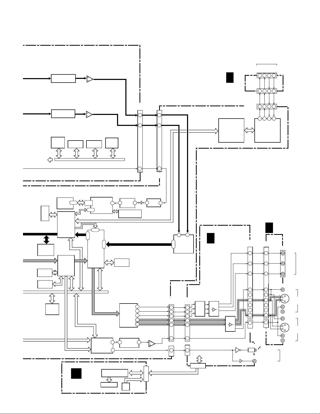
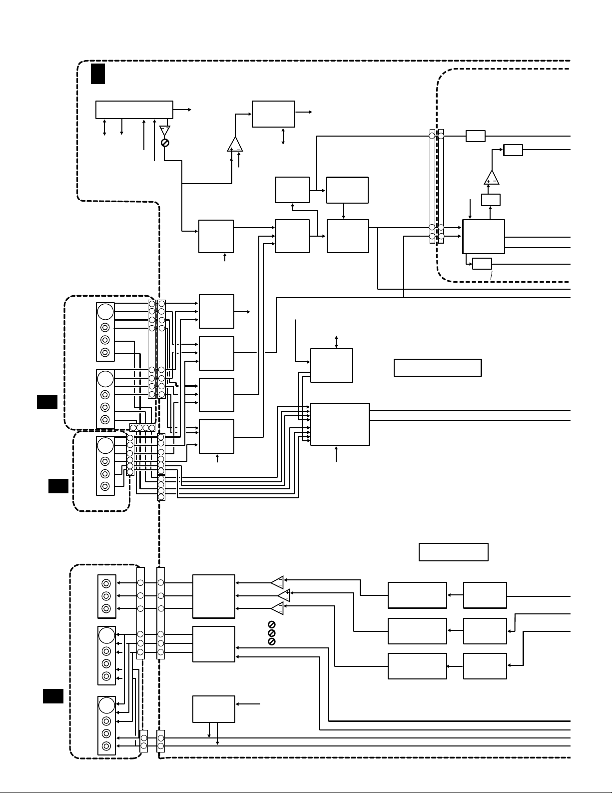
2. BLOCKDIAGRAM AND SCHEMATIC DIAGRAM
2.1 BLOCKDIAGRAM
2.1.1 OVERALL BLOCKDIAGRAM
TU4101 VXF1007
ANT
TV FRONT-END
RF IN
RF
OUT
INPUT3
JA2001
VIDEO
1/2F
D
FRONT
JACK
ASSY(1/2)
Y/C
INPUT1
VIDEO
Y/C
INPUT2
VIDEO
Y/C
Y
C
L
R
JA1522
Y
C
L
R
Y
C
L
R
SIF
OUT
21
CN2002
(12P)
10 10
8
6
1
CN1502
(24P)
16
18
10
14
8
12
21
24
Video Level
VID
OUT
23
CN2003
(12P)
VIN3
YIN3
CIN3
LIN3
CN1002
VIN1
VIN2
YIN1
YIN2
CIN1
CIN2
LIN1
LIN2
ADJ
8
6
1
(24P)
16
7
10
14
8
12
21
24
Tuner Video
Buffer
IC1171
MM1118XF
1
3
4
3
I/BG
TK15404M
from u-com
PDC/VPS
2
16 14
IC7006
Slicer
IC7001
LC74793JM
Selector
IC1004 MN1118XF
5
3
1
IC1003 MN1118XF
5
3
1
IC1002 MN1114XF
5
3
1
A
1/2F
TUMJ ASSY(1/2)
7
DAVI
to u-com
V
7
Y
7
C
7
SN74LV4052APW
TU.V
VIN
YIN
Y/Comp
Selector
IC1103
4
5
2
1
: Recording system signal route
Q1113-Q1115
Q1103,Q1104
V
3
Keyed
Clamp
Q1106
Q1101
IC4702 MSP3417G
SIF
2 27
Stereo
IN
Decoder
Sync
6
Sep.
IC1102
BA7046F
L
OUT
DVD-VR
CN3002(1/2)
(30P)
3
IC1101
TC7WH123FU
UVLO
LIN3
LIN1
LIN2
CN409
(40P)
2
18 18
20 20
5
MMV
C
CN3501(1/2)
Audio Selector
CN3001
(40P)
: Playback system signal route
SECAM ASSY
IC3501
TB1274AF
CVBS
1
C
48
Video
11
Decoder
22
(30P)
Y
LPF/
B
C
C
4
PAL
Encoder
IC3601
MM1394AF
[ATAPI]
DVD-VR
R
3
CVBS
13
IC4202(1/2)
UPC4570G2
Delay
IC4201
BU4052CFV
12
14
15
11
1
8
23
2
20
2
3
E
IC3008
SDRAM
64Mbit
IC3003
PE5219A
ATA I/F
CVBS
1
F
Y
S/CVBS
Selector
IC3222
BU4052BCFV
6
24
24
7
(30P)
(30P)
CN3501(2/2)
CN3002(2/2)
C
6
5
IC4202(2/2)
UPC4570G2
MAIN ASSY
IC9501
PE7003B
DMA I/F
1
7
L
B
1/2F
REAR JACK ASSY
(1/2)
SPDL
MOTOR
Pickup
LD
DRIVE
PICKUP
ASSY
LOADING
M
MOTOR
TILT
M
MOTOR
SLIDER
M
MOTOR
14
CN101
CDA
CDB
CDC
CDD
CDEG
CDFH
DVDA
DVDB
DVDC
DVDD
DVEG
DVFH
CN803
CN801
CN802
(53P)
47
46
29
28
30
26
33
25
(16P)
IC602
PE5131A
IC603
DRAM
16Mbit
IMbit
LB11995
IC313
FLASH
4Mbit
1-2
H.A
96-99
A2-Chip
90-95
IC109
PM0025AF
IC802
SLD/TILT
Drive
M37911FGCHP
7-10
LA6563
IC306
CD/DVD RF
FEP
RF63
IC112
1-4
UPC2511GK
AGCRF
DVDXCD
DEFECT
Detect
DVR-103-PA
DEFECT
IC104
DRAM
4Mbit
Writer
CPU
IC901
ADC08351CIMTC
17
54
B Chip
123
CD/DVD
DECODER
UPD72153AGM
IC315
SRAM
PB CD
8
7
PB DVD
4
3
9
2
IC801
SPDL
Drive
IC804
BA5983FM
BTL
Drive
162-163
A/D
3-10
4-11
53-54
91-92
M63
IC111
15-19,22-26
30-35,46,48,49
DVD-ROM
Encoder
R3-Chip
IC900
PE5214A
NRZI
134
135
139
DVD-VR
CN406
(4P)
1
CD Digital
CN2002
(4P)
4
PE5108A
NRZI
6 5 4
1 2 3
IC2004
178
Slalom
DVD-Video
57-66
DVD-ROM
Dec.
BY-Chip
CD Digital
CN6001
CN407
(6P)
(6P)
IC1011
Backup
SRAM
4Mbit
SDRAM
64Mbit
IC1004
IC2002
DRAM
4Mbit
Flash
32Mbit
IC1008
RECORDER DRIVE MAIN
Page 15
• R ch is same as L ch.
F3242
Y
Y Filter
VTF1166
F3241
C
C Filter
VTF1166
I
C2003
Control
Data
PE5322C9
Tuner
U-com
I
C2010
BR24E16FV
EEPROM
IC3241-1/2
TK15420M
3
2
IC3241-2/2
TK15420M
5
6
I
C5501
BR24E16FV
EEPROM
DVR-7000
DV TERMINAL
XTPB
TPB
XTPA
XPB
XTPB
IC9002
IEEE1394
XTPA
TPA
XPA
JA2003
CN2004
(6P)
CN9001
(6P)
1 2 3 4
1 2 3 4
1 2 3 4
34 35 36 37
TSB41AB2PAP
Physical IC
1
D
2/2
FRONT JACK ASSY(2/2)
CN3001
7
I
C2008
RV5C386A
Real
Time
Clock
(10P)
SEL.Y
10
8
L
1
SEL.C
SEL.L
10
8
1
CN8001
(10P)
IC9001
TSB42AB4PDT
IEEE1394
Link IC
UPD61003
DDCE
Audery
DV Codec
SDRAM
64Mbit×2
IC5003,IC5004
IC5005
DVXCEL-BA1
Stream
Check
IC4003
IC4004
DRAM
16Mbit×2
IC4001
SDRAM
16Mbit
HD6417709AF100B
MPEG Video
IC9502
UPD65954GC
–E59–7EA
M65774BFP
Main
CPU
I
C1010
IC4007
IC6002
Encoder
DVxcel
AV
Decoder
AV-1
44-68
F
IC6003(1/2)
PE7004A
84-101
104-107
18-24
55-64
117
|
126
Video
Pre/Post
Graphic
Engine
Vaikilt
FL
ASSY
PCM18001-1
15
129
Audio I/F
Aprilia
44
|
54
IC4006
PD6342A
Sampling Rate
IC4005
SDRAM
64Mbit
IC6003(2/2)
PE7004A
2 16
126
Audio I/F
31
Aprilia
IC1201 MSM9202-01
FL Driver
FL
V1201
IC8003
Audio
A/D
48KHz 20Bit
Converter
NTSC/PAL
Encoder
IC7003
PM0030A
IC8011
PCM1716
Audio
D/A Conv.
Key
SW
IC8001
1
101
99
103
6
10
CN1202
(20P)
IC8002
TC9412AF
3
ER-VR
IC6004
CS8420-CS
P
B
P
R
Y
Y
C
2
3
IC8010-1/2
UPC4570G2
4
REAR JACK ASSY(2/2)
2/2F
Y
P
B
P
R
VOUT2
VOUT1
YOUT2
YOUT1
COUT1
COUT2
LOUT
B
CN1501
(24P)
6
4
2
18
17
21
20
23
24
6
CN1502
OPTICAL
COAXIAL
JA1501
JA1521
Y
C
Y
C
AC-3/PCM
DIGITAL
AUDIO
OUT
Y
P
B
P
R
VIDEO
L
R
VIDEO
L
R
COMPONENT
VIDEO OUT
LINE
OUT 2
LINE
OUT 1
135
122
A
56
63
CN7001
(22P)
13
15
11
3
5
|
Decoder
George
IC8008
PD0272A
B
OUT
P
R
OUT
P
Y/G OUT
Y OUT
C OUT
Video
CN1003
(22P)
10
8
12
20
18
F1201
-F1206
Filter
2/2F
TUMJ ASSY(2/2)
IC1901/IC1902
TK15420M
IC1312
TK15453V
IC1351
BA7665FS
CN1001
(24P)
6
4
2
18
17
21
20
23
24
6
CN1002
L OUT
22 1
1
CN2001
CN2010
PCM OUT
12 9
Tuner U-com
IC1421
JA1401
JA1411
Q1411
CN2009
(20P)
15
Page 16
DVR-7000
2.1.2 TUJB BLOCKDIAGRAM
TUMJ ASSY (VWV1897)
A
F
TU4101
V/U Tuner Module
VXF 1007-
AFT
SCL
<u-com>
SDA
JA1522
IN1
JA1522
REAR JACK ASSY(1/2)
JA1521
(VWV1883)
F
IN2
B
JA2001
IN3
(Front)
F
D
S
C
Y
Comp
L
R
S
C
Y
Comp
L
R
CN1502
S
C
Y
Comp
L
R
4
6
8
10
1
3
CN2002
XPAL
CN1502
23
20
3
XSECAM
9
8
10
10
16 16
13 13
12 12
14
14
18
18
21
24
4
6
10
1
3
24
21
23
20
CN1002
9
8
8
CN1002
4
2
CN2003
IC4101
TK15404M
Tuner
Video Level
VR4141
SIF
<IC4702>
1
IC1171
Tuner Video
Buffer
MM1118XF
to IC4201
Pin12
Pin 1
<u-com>
5
IC1001
S-Selector
1
2
74LV4052
3
IC1002
C-Selector
1
5
MM1114XF
3
IC1003
Y-Selector
1
MM1118XF
5
3
IC1004
Comp
1
Selector
5
MM1118XF
LISEL1
LISEL2
4
XCVBS
TUSEL 2
16
2
IC7006
TK15404M
3
I/BG
from u-com
7
XSELS
3
<u-com>
7
7
7
<u-com>
IC7001
PDC/VPS
Slicer
LC74793JM
6,7
4
1,2
5
SCL
SDA
IC1102
Sync-Sepa
BA7046F
6
IC1103
Y/Comp
Selector
74LV4052
SIF
<TU4101>
14
DAVI
<u-com>
2
3
3
12,13
IC4702
2
Stereo
Decoder
27
MSP3417G
28
15
11
IC4201/4202/IC4302
14
Line Input
12
Audio Selector
2
4
5
1
BU4052 & uPC4570
IC1101
MMV
TC7WH123FU
5
Keyed Clamp
(Discrete)
<u-com>
SCL
SDA
9,10
LISEL1
LISEL2
<u-com>
Y/CVBS
Audio Input Circuit
L
13
3
R
IC3651
SN74AHC2G14HDCT
CN3002(1/2)
CN3501(1/2)
22
22
<u-com>
CVBS
18
18
1
C
20 20
48
VS
IC3511
TC7WH123FU
Logic
F3551
VTF1176
1
32
SCL
SDA
LPF
Y
IC3501
Video Decoder
TB1274AF
4
Logic
CSYNC
Delay
IC3551
1113,14
22
23
IC3512
TC7W32F
TK15420M(1/2)
Pb
Pr
FRONT JACK ASSY
(VWV1890)
JA1501
Component
OUT
JA1521
OUT2
REAR JACK ASSY(2/2)
(VWV1883)
CN1501
F
B
OUT1
16
Y
C
Comp
Output Circuit
CN1001
13
Y
14
Comp
CN1002
P
B
P
R
Y
C
L
R
IC1312
30MHz
9
Video Driver
11
TK15453V
15
IC1351
Video Driver
9
12
BA7665FS
(Discrete)
Muting
6
6
4
4
2
2
21
21
24
24
17
17
CN1502
6
6
4
4
2
7
6
4
2
1
Y
7
C
AMUTE
<MAIN>
1
Y Level
P
P
B
R
5
6
3
2
TK15420M
Level
Level
IC1901
TK15420M(1/2)
IC1901
3
TK15420M(2/2)
2
IC1902
F1202
Y interlace Filter
VTF1166-
F1204
P
B
Interlace Filter
VTF1166-
F1206
P
R
Interlace Filter
VTF1166-
Video Buffer
(Discrete)
Video Buffer
(Discrete)
Video Buffer
(Discrete)
Page 17
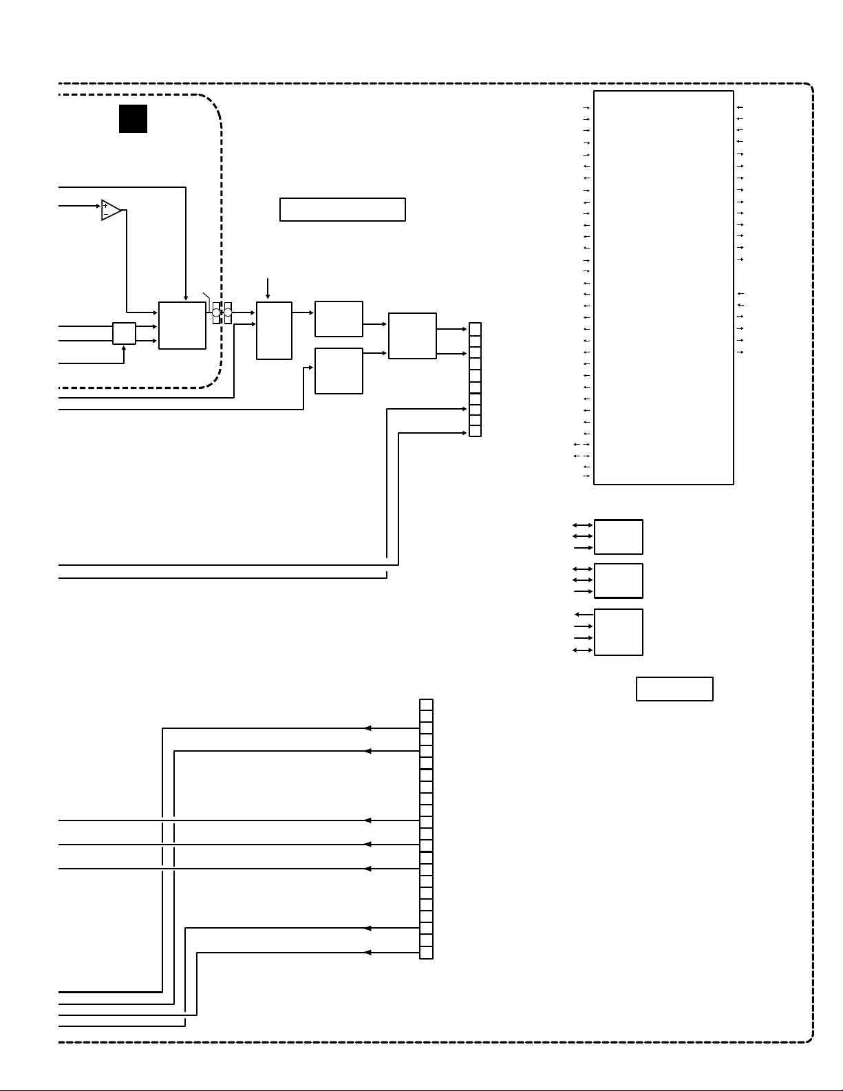
DVR-7000
C
SECAM ASSY
(VWV1892)
5
7
IC3551
6
TK15420M(2/2)
CSYNC
20
4
Discrete
Filter
IC3601
PAL Encoder
3
2
MM1394AF
CN3002(2/2)
CN3501(2/2)
24
24
Y/CVBS
CVBS
Video Input Circuit
<u-com>XFSECAM
5
6
7
IC3222
PAL/
SECAM
Selector
TC4W53
Y/CVBS
1
C
F3242
Y Filter
VTF1166-
F3241
C Filter
VTF1166-
Y/CVBS
C
IC3241
Video AMP
3
5
TK15420M
SELY
1
SELC
7
SELR
SELL
10
CN3001
9
<to MAIN>
8
7
6
5
4
3
2
1
<TUMJI/F>
32K
XINTRA
XINTRB
NLINKI
AFT
RSTCTL
IOC
SLICE
STBYQ
DAVI
XPAL
XSECAM
P_ON
FANDET
XSELS
VI_ON
TUSEL1
TUSEL2
XCBVS
SCHNG
XFSECM
LISEL1
LISEL2
FANON
TUON
AMONLY
SQEEZE
LET S
WRT PRT
SCL
SDA
I/BG
TEST
IC2003
Tuner Control u-Con
PE5322C9
<FLKBI/F>
JOGA
JOGB
KEY1
KEY2
TIMER
DVDLED
FLOFF
DOLBY
FLCS
XFLRST
FLDATA
FLCP
FLDIM1
FLDIM2
<MAIN I/F>
RXD1
ACSK1
TXD1
TUREQ
ZRESET
AV1RST
SCL
SDA
WRTPRT
SCL
SDA
WRTPRT
32K
XINTRA
XINTRB
SCL
IC2010
EEP-ROM
BR24E16
IC5501
EEP-ROM
BR24E16
IC2008
Real-Time
Clock
RV5C386A
SDA
u-com I/F
22
Y
C
Y
P
B
P
R
R
L
CN1003
21
20
19
18
17
16
15
14
13
12
11
10
9
8
7
6
5
4
3
2
1
<from MAIN>
17
Page 18
DVR-7000
2.1.3 POWER BLOCKDIAGRAM
MAIN ASSY
E
F
AC IN
LIVE
NEUTRAL
CN101
F101
3.15A/125V
T102
T101
SW+2_5V
SW+3_3V
SW+13V
SW+12V
SW+6V
EV+17V
EV+37V
EV+6V
SW+5V
FL AC
FL AC
FL-37V
PW ON
CN201
3
4
7
8
10
13
CN202
1
3
5
7
9
11
15
CN203
1
2
5
6
SW+2_5V
SW+2_5V
SW+3V
SW+3V
SW+6V
SW+13V
CN2003
3
4
7
8
10
13
F2008
F2007
V+2D
F2006
F2009
V+12V
IC1003
1
V+3D
V+1_9D
IC7201
V+6D
V+13V
CN7001
IC2008
IC2006
IC2007
V+2Q
V+5D
V+5A
V+12A
I
POWER
SUPPLY ASSY
CN204
1
2
3
5
SW+5V
SW+5V
SW+12V
SW+12V
CN403
1
2
5
6
IC408
F404
V+5M
V+5D V+5A
IC409 IC401
V+12M V+8
V+3A V+3D
IC406 IC405
IC407
F401
F406
V+5U
R409
RECORDER DRIVE MAIN
V+5L
V+5P
R408
18
Page 19

SW+6V
SW+13V
EV+17V
EV+35V
EV+6V
SW+2_5V
POWER ON
A
CN2001
1
3
5
7
9
11
15
CN1003
22
TUMJ ASSY
F
V+6V
R2005
R2007
POWER ON
from µ-com
R2014
V+2_5V
R2031
V+12V
V+6E
V+13V
IC2002
Q3431
IC2011
Q2005
Q2006
Q2007
V+3_3E
V+5VR
Q1831
R2004
D2073
D2074
Q4401
Q4411
V+12V
V+5VC
F2008
V+5VO
V+17V
Q2002
Q2004
F1821
V+3_3M
R1011
R2010
V+3_3V
V+5VM
V+35V
V+5VI
V+5E
V+5TUA
R4410
IC4402
V+12VO
V+12AI
VREF
V+17V
V+13V
F2007
F2009
V+17FAN
V+13FAN
CN2006
1
CN2007
1
DVR-7000
FAN MOTOR
VXM1092
FAN MOTOR
RXM1090
CN1201
FLAC1
FLAC2
VFDP
V+13V
F
FL ASSY
V+6E
V+3_3V
D2041
16 1
1
2
3
5
F L
FL
Dimmer
V+13V
CN1203
H
CN2009
5 20
V+5E
V+3_3E
CN1202
V+3_3E
4
V+3_3E
4
CN1001
V+3_3E
SW ASSY
V+5E
1
CN1204
4
C
SECAM
ASSY
V+5E
V+3_3E
4
1
V+3_3E
8 10
8 10
CN1101
V+5E
V+12V
V+5VR
12
V+12V
V+5VM
V+5VM
12
V+12VS
G
JOG
ASSY
CN3002
CN3501
V+5VS
19
Page 20

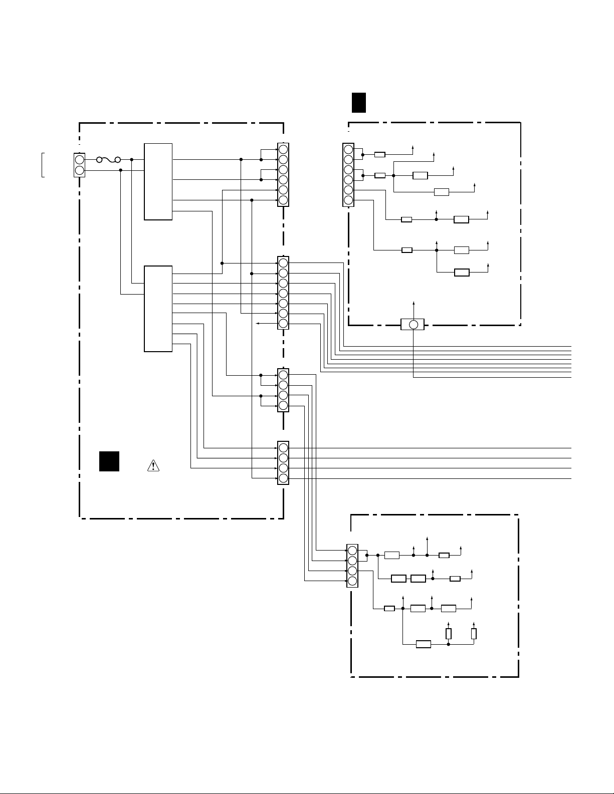
DVR-7000
2.2 OVERALL WIRING DIAGRAM
D
F
FRONT JACK ASSY
(VWV1890)
SW ASSY
H
(VWG2315)
CN1001
FL ASSY
(VWG2314)
CN1201
G
CN1203
F
CN1202
CN1204
CN1101
JOG ASSY
(VWG2316)
DV Terminal
CN2002
CN2004
CN2009
CN2007
CN1003
CN7001
CN2003
C
CN3501
CN3002
A
A 1/4F – 4/4F
F
TUMJ ASSY
(VWV1897)
SECAM ASSY
(VWV1892)
CN2010
CN2001
CN409
RECORDER DRIVE
MAIN
(DWX2148)
This service manual
does not include
this recorder section.
Refer to the S/M for
DVR-A03(RRV2423).
CN403
CN406
CN407
CN3001
E
E 4/10F,7/10F,8/10F,10/10F
F
MAIN ASSY
(VWV1895)
CN8001
CN2002
CN9001
20
Page 21

DVR-7000
Note : When ordering service parts, be sure to refer to "EXPLODED VIEWS and P AR TS LIST" or "PCB PARTS LIST".
CN2006
CN3001
CN8001
VKP2276
CN2003
CN2001
CN202
CN201
CN1001
CN1002
CN1501
CN1502
REAR JACK ASSY
B
F
(VWV1883)
I
POWER SUPPLY ASSY
(VWR1348)
CN2004
CN203
CN204
CN101
21
Page 22

1
23
DVR-7000
2.3 TUMJ ASSY(1/4) AND REAR JACK ASSY
CN7001
A
E 7/10F
B
CN1003
A
3/4F
A
1/4F
)
)
B
R
(P
(P
(C-Y)
TUMJ ASSY(1/4)
(VWV1897)
(S-Y)
2SA1576A(QR)
Q1103
E
B
C2
C
E2
(S-C)
(S-Y)
Keyed Clamp
E2
Q1101
HN1A01FU(YGR)
C2
B1
Q1104
2SK210(Y)
Q1115
Q1115
HN1C01FU(YGR)
HN1C01FU(YGR)
B2
Q1101
B1
HN1A01FU(YGR)
B2
C
Q1114
HN1C01FU(YGR)
E
C
B
E
C2
E2
Q1101
E
C
B2
HN1A01FU(YGR)
Q1114
HN1C01FU(YGR)
E2
C2
Q1223
HN1A01FU(YGR)
C
B
E
2SA1576A(QR)
E2
C2
Q1227
HN1A01FU(YGR)
C
B
E
2SA1576A(QR)
E2
C2
Q1231
HN1A01FU(YGR)
C
B
E
2SA1576A(QR)
B2
Q1203
B2
Q1207
B2
Q1211
4
Output Filter
E
B
Q1223
C
HN1A01FU(YGR)
Y-Interlace
E
B
Q1227
C
HN1A01FU(YGR)
Pb-Interlace
E
B
Q1231
C
HN1A01FU(YGR)
Pr-Interlace
B2
Q1224
HN1A01FU(YGR)
Q1224
HN1A01FU(YGR)
B2
Q1228
HN1A01FU(YGR)
Q1228
HN1A01FU(YGR)
B2
Q1232
HN1A01FU(YGR)
Q1232
HN1A01FU(YGR)
E2
C2
E
B
C
E2
C2
E
B
C
E2
C2
E
B
C
A
3/4F
E
C
B
Q1106
DTA124EUA
(S-Y)
(S-C)
C
(S-C)
A
3/4F
(S-Y)(Comp)
Q1101
E2
HN1A01FU
B1
B2
Q1101
HN1A01FU
Q1106
2SA1576A(QR)
1
(S-Y)(Comp)
D
A
2/4F
A
4/4F
B
Q1172
DTC124EUA
C
E
V/U(Comp)
C1
3
2
(S-C)
(S-Y)
(S-Y)
(Comp)
(Comp)
(S-C)
(S-C)
(S-Y)
(S-Y)
(Comp)
(Comp)
22
A 1/4F
1234
Page 23

5
678
DVR-7000
(C-Y)
(PB)
(PR)
Q1831
2SD1884(PQR)
3
2
1
Component Y
Level Adj.
B
Level Adj.
P
R
Level Adj.
P
(C-Y)
(PB)
(PR)
(Comp)
(S-C)
(Comp)
: COMPOSITE VIDEO SIGNAL ROUTE
(S-Y)
: S–Y VIDEO SIGNAL ROUTE
(S-C)
: S–C VIDEO SIGNAL ROUTE
(C-Y)
: COMPONENT Y SIGNAL ROUTE
(PB)
: COMPONENT PB SIGNAL ROUTE
(PR)
: COMPONENT PR SIGNAL ROUTE
(D)
: DIGITAL AUDIO SIGNAL ROUTE
: AUDIO SIGNAL ROUTE(L ch)
JA1501
JA1521
A
A
2/4F
(D)(D)
Q1411
2SC4081(QR)
(D)
B
JA1401
C
E
NOTE
R
without notice
C
without notice
CE
without notice
JA1411
C
B
Q1311
E
2SC4081(QR)
(PR)
(PB)
(C-Y)
CN1001
CN1501
(S-Y)
B
(Comp)
(S-Y)
(S-C)
(S-Y)
(S-C)
B
Q1341
DTC124EUA
C
B
Q1504
2SD2114(VW)
E
B
C
Q1505
B
B
B
C
C
E
Q1501
2SD2114(VW)
E
C
Q1503
2SD2114(VW)
2SD2114(VW)
(S-Y)
(S-C)
(S-C)
(Comp)
(S-Y)
JA1522
C
C
E
CN1002
(S-C)
(S-Y)
(Comp)
CN1502
Q1502
2SA1576A(QR)
E
D
REAR JACK ASSY
B
F
(VWV1883)
5
6
7
A 1/4F
B F
8
23
Page 24

1
DVR-7000
2.4 TUMJ ASSY(2/4)
23
4
A
B
CN2006
to FAN
CN2007
to FAN
A
NOTE
R
without notice
C
without notice
CE
without notice
C
Q2009
E
2SD2114K(VW)
2/4F
B
TUMJ ASSY(2/4)
(VWV1897)
C2
B2
E2
Q2202
HN1C01FU(YGR)
HN1C01FU(YGR)
Q2014
RN2903
E
E2
C
B2
C2
C
E
Q2202
Q2014
RN2903
Q2203
2SC4081(QR)
C
B
B
B
E
C
B
Q2010
E
2SD2114K(VW)
Q2021
DTA124EUA
C
B
C
B
C
Q2024
DTC124EUA
E
C
B
E
B
E
C
E
Q2022
E
2SD2114K(VW)
Q2023
2SC4081(QR)
Tuner Control U-com
Reset IC
CN1202
F
CN2009
D
EEPROM
A
1/4,3/4,4/4F
24
A 2/4F
1234
Page 25

5
678
DVR-7000
Q2004
2SD1664(PQR)
3
2
1
(D)
: DIGITAL AUDIO SIGNAL ROUTE
A
CN2001
Q2012
HN1K03FU
Q2008
HN1K03FU
B
Q2003
DTC143EUA
Q2006
2SB1132(QRS)
2
2
3
2
1
B
C
E
Q2001
DTA124EUA
3
Q2007
2SD1664(PQR)
E
C
1
Q2005
DTC143EUA
3
1
C
B
E
CN2008
CN202
I
B
for DATA Loading
C
B
Q2013
E
DTC124EUA
Q2015
HN1K03FU
C
Real Time Clock
5
Q2016
HN1K03FU
CN2010
CN2001
A
1/4F
(D)
E 2/10
D
: The power supply is shown with the marked box.
6
7
8
A 2/4F
25
Page 26

1
23
DVR-7000
2.5 TUMJ ASSY(3/4) AND SECAM ASSY
4
A
B
CN3001
CN8001
E 8/10F
(S-C)
A
3/4F
TUMJ ASSY(3/4)
(VWV1897)
4/4F
A
NOTE
R
without notice
C
without notice
CE
without notice
(S-Y/Comp)
Q3431
2SD1664(PQR)
3
2
1
(S-C)
(S-Y/Comp)
C
CN3501
(S-C)
B
C
Q3221
2SC4081(QR)
E
A
CN3002
4/4F
1/4F
A
Q3222
2SC4081(QR)
C
B
E
D
A
2/4F
(S-Y/Comp)
Q3223
DTA124EUA
C
E
HN1A01FU(YGR)
E2
Q3212
B2
C2
B
HN1A01FU(YGR)
Q3212
E
B
C
E
B
C
Q3211
2SA1576A(QR)
A
(S-Y/Comp)
(S-C)
1/4F
(S-Y/Comp)
26
A 3/4F
C
1234
Page 27

Video
Decoder
IC
5
678
DVR-7000
(Comp)
: COMPOSITE VIDEO SIGNAL ROUTE
(S-Y)
: S–Y VIDEO SIGNAL ROUTE
(S-C)
: S–C VIDEO SIGNAL ROUTE
: AUDIO SIGNAL ROUTE(L ch)
A
B
NTSC/PAL Encoder
Q3501
RN1903
B2
C
B
Q3501
RN1903
E
C2
E2
E
B
Q3531
C
2SA1576A(QR)
E
B
C
Q3541
2SA1576A(QR)
Q3571
2SC4081(QR)
(S-Y/Comp)
(S-C)
(S-Y/Comp)
E
B
C
Q3573
2SA1576A(QR)
(S-C)
Q3551
2SA1576A(QR)
B
Q3572
2SC4081(QR)
B
E
C
C
E
B
E
C
Q3574
2SA1576A(QR)
SECAM ASSY
C
(VWV1892)
680
C
(S-Y/Comp)
D
5
6
7
8
A 3/4F
C
27
Page 28

1
23
DVR-7000
2.6 TUMJ ASSY(4/4) AND FRONT JACK ASSY
NOTE
R
without notice
C
without notice
4
A
VHF/UHF TUNER
Q4102
Q4104
2SC4081(QR)
HN1B01FU(YGR)
C2
B2
HN1B01FU(YGR)
E2
Q4107
HN1K03FU
Q4104
B
E
C
E
B
B
C
(SIF)
(Comp/VU)
C
B
Q4161
E
B
Q4108
2SC4081(QR)
2SC4081(QR)
C
E
Q4162
2SC4081(QR)
C
B
E
Q4103
HN1B01FU(YGR)
B2
E
B
C
Q4103
HN1B01FU(YGR)
C2
E2
Terrestrial Video
Level Adj.
(SIF)
(Comp/VU)
CE
without notice
Q4406
2SD1664(PQR)
3
2
1
Q4411
2SB1132(QRS)
Q4401
2SD1664(PQR)
2
3
1
3
1
2
2SB1132(QRS)
3
1
2
Q4413
C
DTC143EUA
C
E
Q4414
DTC143EUA
E
Q4412
B
B
Q7001
HN1K03FU
C
Q7002
DTC124EUA
C
B
E
A
4/4F
VPS/PDC
Data Slicer
TUMJ ASSY(4/4)
(VWV1897)
EEPROM
D
JA4501
JA4502
28
A 4/4F
1234
Page 29

5
678
DVR-7000
Q4301
2SD1664(PQR)
3
2
1
Q4304
HN1A01FU(YGR)
B2
E
E2
C2
B
C
Q4355
2SD2114K
C
B
E
(Comp)
(S-Y)
(S-C)
CN2003
CN2002
(S-Y)
(S-C)
(Comp)
JA2001
A
JA2002
Stereo
Decoder
Q4305
HN1A01FU(YGR)
B2
Q4601
HN1K03FU
E
E2
C2
B
C
C
E
Q4305
HN1A01FU(YGR)
B
Q4345
2SD2114K
Q4308
2SA1576A
E
C
CN2004
E 9/10
CN9001
B
FRONT JACK ASSY
D
F
JA2003
DV TERMINAL
B
(VWV1890)
A
3/4F
A
3/4F
C
A
3/4F
C
Q4201
RN1903
B
C2
E
B2
Q4201
E2
RN1903
Audio Selector
(Comp)
: COMPOSITE VIDEO SIGNAL ROUTE
(S-Y)
: S–Y VIDEO SIGNAL ROUTE
(S-C)
: S–C VIDEO SIGNAL ROUTE
A
2/4F
A
1/4F
D
: AUDIO SIGNAL ROUTE(L ch)
: The power supply is shown with the marked box.
5
6
7
8
A 4/4F D F
29
Page 30

1
DVR-7000
2.7 MAIN ASSY(4/10)
A
23
(PB-DV)
(PB-DV)
(REC-DV)
(PB-DV)
(PB-DV)
(REC-DV)
4
E
5/10
E
7/10F
E
E
5/10
8/10F
5/10,9/10
E
1/10
E
E
1/10
E 4/10F
64M SDRAM
B
• Parts R45 is assembled
to PCB cell F4005
• Parts R48 is assembled
to PCB cell F4008
• Parts R49 is assembled
to PCB cell F4009
(PB-DV)
MAIN ASSY
(VWV1895)
Video Pre/Post LSI
C
D
(PB-DV)
(REC-DV)
(PB-D)
(PB-DV)
(REC-DV)
(PB-D)
30
(PB-DV)
E
9/10
E
3/10,8/10F
(REC-DV)(PB-DV)
: PB DATA SIGNAL ROUTE
: PB DIGITAL VIDEO SIGNAL
ROUTE
: REC DIGITAL VIDEO SIGNAL
ROUTE(Analog Input)
: PB DIGITAL AUDIO SIGNAL
ROUTE
E 4/10F
1234
Page 31

5
678
DVR-7000
A
16M SDRAM
16M SDRAM
16M EDO DRAM
16M DRAM
(PB-D)
(PB-DV)
(PB-D)
(PB-DV)
(PB-D)
(to DAC)
E
3/10
E
E
E
E
1/10
3/10
B
6/10
1/10
C
(PB-D)
(to SPD/IF)
MPEG2 Decoder IC
E
3/10
E
3/10
D
5
6
7
8
E 4/10F
31
Page 32

1
DVR-7000
2.8 MAIN ASSY(7/10)
A
IC7004 M32L1632512A-8Q and IC7006 PM0024AF is deleted.
B
23
4
C
D
32
E 7/10F
1234
Page 33

5
678
DVR-7000
3
Q7001
2SA1576A(QR)-TLB
1
2
Video Encoder IC
3
1
2
Q7002
C Level Adj.
2SA1576A(QR)-TLB
CVBS Y Level Adj.
E 3/10
E
E
4/10F
E
1/10
E
2/10
8/10F
A
B
E 7/10F
MAIN ASSY
(VWV1895)
(Y)
:
Y VIDEO SIGNAL ROUTE
(C)
:
CHROMA VIDEO SIGNAL ROUTE
(C-Y)
:
COMPONENT Y SIGNAL ROUTE
(PB)
:
COMPONENT PB SIGNAL ROUTE
(PR)
:
COMPONENT PR SIGNAL ROUTE
:
AUDIO SIGNAL ROUTE(L ch)
3
1
2SA1576A(QR)-TLB
2
Q7007
R
Level Adj.
P
)
R
(P
(C-Y)
)
B
(P
Component
Y- Level Adj.
33
3
1
2SA1576A(QR)-TLB
2
Q7005
3
1
2SA1576A(QR)-TLB
2
(C)
Q7003
3
1
2
PB Level Adj.
Q7004
2SA1576A(QR)-TLB
(PB-DV)
(C-Y)
(PB)
(PR)
CN1003
A 1/4F
CN7001
(Y)
(C)
C
(Y)
Q7009
3
1
2SA1576A(QR)-TLB
2
:
The power supply is shown with the marked box.
5
6
7
8
E 7/10F
33
D
Page 34

1
DVR-7000
2.9 MAIN ASSY(8/10)
23
4
A
CN8001
B
CN3001
A 3/4F
TUJK Input Level
pedestal : +4V
P-P value : 2Vpp
(REC)
Side A
Q8002
2SA1576A(QR)-TLB
Electric VR
Q8001
F863
2SC4081(QR)-TLB
1
3
1
2
2
3
2
1
2SC4081(QR)-TLB
3
Q8005
A/D
470
470470
(REC-D)
E 8/10F
MAIN ASSY
(VWV1895)
(REC-DV)
: REC DIGITAL VIDEO SIGNAL ROUTE
(REC-V)
: REC ANALOG VIDEO SIGNAL ROUTE
(REC-D)
: REC DIGITAL AUDIO SIGNAL ROUTE
(PB-D)
: PB DIGITAL AUDIO SIGNAL ROUTE
(REC)
: REC ANALOG AUDIO SIGNAL ROUTE(Lch)
B
)
(P
: PB ANALOG AUDIO SIGNAL ROUTE(Lch)
3
1
2
Q8006
2SA1576A(QR)-TLB
C
Q8009
2SC4081(QR)-TLB
Q8011
2SC4081(QR)-TLB
1
2
3
Q8008
DTC143EUA-TLB
DAC
(PB-D)
D
1
R808
VCH1235
0
3/10
E
2
3
2
1
3
220P
VCH1235
220P
VCH1235
56P
56P
C826
(PCB silk is R8216.)
220P
(PB)
34
E 8/10F
1234
Page 35

5
678
DVR-7000
E
E
1/10
E
1/10
3/10
E
E
6/10
4/10F
A
B
(REC-D)
(REC-DV)
E
3/10
(REC-V)
(REC-V)
E
3/10
Video Decoder
E
1/10
C
(REC-DV)
E
7/10F
E
6/10
2/10
8
E
35
E
E 8/10F
5
6
7
D
1/10
Page 36

1
DVR-7000
2.10 MAIN ASSY(10/10)
A
23
4
E 10/10F
MAIN ASSY
(VWV1895)
B
(PB-D)
E
3/10
(REC-D)
Note : IC9501 Peripheral Mount Direction
Not used
Not used
Not used
Not used
(PB-D)
DMA I/F LSI
E
3/10
C
Not used
(REC-D)
D
36
E 10/10F
1234
Page 37

5
678
DVR-7000
E
1/10
E
3/10
E
4/10F
E
E
3/10
E
2/10
E
6/10
9/10
A
B
(REC-D)
1/10
E
5/10
E
9/10
E
5/10
E
C
EPLD
5
6
7
(REC-D)
(REC-DV)
(PB-D)
: REC DATA SIGNAL ROUTE
: REC DIGITAL VIDEO SIGNAL ROUTE
: PB DATA SIGNAL ROUTE
E 10/10F
8
37
D
Page 38

1
CN3001
CN1003
CN2006
CN2001
23
DVR-7000
3. PCB CONNECTION DIAGRAM
3.1 TUMJ ASSY
A
CN2003
CN2002
D
B
CN3002
CN3501
C
4
CN2009
CN1202
F
A
TUMJ ASSY
F
NOTE FOR PCB DIAGRAMS :
1. Part numbers in PCB diagrams match those in the schematic
diagrams.
C
2. A comparison between the main parts of PCB and schematic
diagrams is shown below.
Symbol In PCB
Diagrams
BCE
BCE
D
Symbol In Schematic
Diagrams
BCEBCE
BCE
DGG
S
BCE
DG
S
Transistor
Transistor
with resistor
S
Field effect
transistor
Resistor array
3-terminal
regulator
Part Name
(VNP1845-B)
3. The parts mounted on this PCB include all necessary parts for
several destinations.
For further information for respective destinations, be sure to
check with the schematic diagram.
4. View point of PCB diagrams.
Connector
Capacitor
SIDE A
P.C.Board
Chip Part
SIDE B
CN2010
CN2001
E
CN8001
CN7001
FAN
MOTOR
FAN
MOTOR
E
E
CN2007
D
I
CN202
38
SIDE A
A F
1234
Page 39

5
678
DVR-7000
A
Q2008
Q3221
IC6001
IC3222
Q2012
IC4701
Q2203
IC6002
IC2001
IC7001
Q2014
Q4201
Q7001
IC2010
Q4301
IC7006
IC7003
Q7002
IC2008
IC2004
IC1103
IC2012
Q2002
Q2001
Q2003
Q2013
IC2005
Q3222
Q4104
Q4401
IC2301
Q3431
IC2003
Q1953
Q4355
Q1951
IC7002
IC5501
Q1103
IC4402
Q2007
IC2007
Q2015
IC1171
Q2022
IC2006
IC2009
Q3212
Q3223
Q4406
Q4013
IC4011
Q4413
IC4201
Q1115
Q2202
Q1114
IC1951
Q4308
IC2002
IC1102
Q2024
Q1108
Q4102
IC3241
Q4107
Q4601
IC4702
Q4414
Q1113
Q1952
Q2016
Q2021
IC2017
Q2006
Q4411
Q2005
Q1105
Q1101
Q1106
B
CN3001
CN1003
CN2007
CN2006
CN1002
CN1502
F
B
CN1001
IC1001
IC1101
Q1411
IC1004
IC1421
IC1002
Q1227
Q1231
Q1901
IC1902
Q2004
Q1331
Q1342
IC1351
Q1334
Q1335
Q1311
Q1312
Q2010
Q2011
Q1224Q1225
IC1003
Q1228
Q1231
IC1051
Q1831
Q2009
C
D
CN2001
CN1501
F
B
5
6
7
8
A F
39
Page 40

A
IC1371
IC2013
Q1211
Q1207
Q1203
Q1172
Q8001
Q4345
IC4202
IC4302
Q4161
Q4108
CN3001
1
10
CN2001
CN1001
CN1002
1
24
1
24
1
16
CN2006
1
1
CN2007
B
1
DVR-7000
23
4
C
D
40
A F
1234
Page 41

5
678
DVR-7000
A
CN2003
1
CN2009
B
20
SIDE B
(VNP1845-B)
A
TUMJ ASSY
F
C
D
5
6
7
8
A F
41
Page 42

1
23
DVR-7000
3.2 REAR JACK, SECAM and FRONT JACK ASSYS
REAR JACK ASSY
B
F
A
FRONT JACK
D
F
ASSY
4
CN2003
CN2002
F
A
CN1001
F
CN1501
A
CN2004
CN9001
B
CN1002
F
CN1502
E
(VNP1845-B)
A
(VNP1845-B)
C
SECAM ASSY
C
D
CN3002
A
F
42
C
B F
1234
D F
IC3511IC3501
IC3512
CN3501
Q3573
Q3574Q3551Q3501
SIDE A
Q3571
Q3572
IC3551
IC3651
IC3601
(VNP1845-B)
Page 43

1
FRONT JACK
D
F
ASSY
CN2002
234
DVR-7000
REAR JACK ASSY
B
F
A
(VNP1845-B)
CN2004
Q1505
Q1503
Q1504
Q1502
Q1501
CN1501
B
CN1502
(VNP1845-B)
C
SECAM ASSY
C
IC3621 Q3541 Q3531
1
30
CN3501
SIDE B
2
1
D
(VNP1845-B)
C
3
B F
D F
4
43
Page 44

DVR-7000
4. ADJUSTMENT
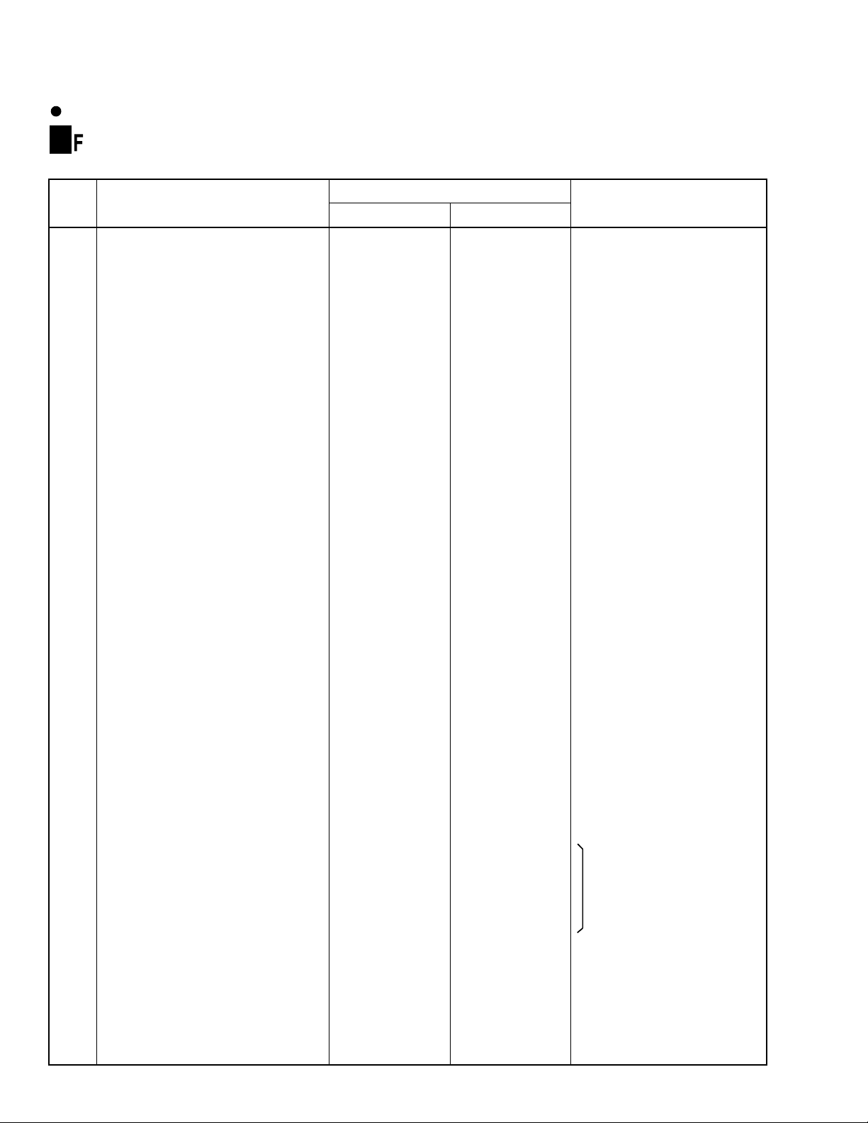
4.1 TUMJ ASSY ADJUSTMENT
Note : Use disc : [ DVD PAL test disc ]
No. Adjustment Name
Video level adjustment of terrestrial
1
wave (Input system adjustment)
Y level adjustment of component system
2
(Output system adjustment)
PB level adjustment of component system
3
(Output system adjustment)
PR level adjustment of component system
4
(Output system adjustment)
When NTSC test disc GGV1025 is used, the adjustment No.2 to No.4 value is changed to the following value.
No. Adjustment Name
Y level adjustment of component system
2
(Output system adjustment)
PB level adjustment of component system
3
(Output system adjustment)
PR level adjustment of component system
4
(Output system adjustment)
It is recommended to adjust using PAL disc.
Adj. Point Measurement Point
VR4141
VR1901
VR1902
VR1903
TUMJ ASSY
CN3001 Pin10(SEL Y)
Component ouput (Y)
(75Ω terminate)
Component ouput (PB)
(75Ω terminate)
Component ouput (PR)
(75Ω terminate)
Adj. Point Measurement Point
VR1901
VR1902
VR1903
Component ouput (Y)
(75Ω terminate)
Component ouput (PB)
(75Ω terminate)
Component ouput (PR)
(75Ω terminate)
Adjustment Value
2.00Vp-p ± 100mV
1.0Vp-p ± 40mV
700mVp-p ± 28mV
700mVp-p ± 28mV
Adjustment Value
980mVp-p ± 39mV
525mVp-p ± 21mV
525mVp-p ± 21mV
Adjustment State
Input a signal of PAL-I/White 100% 70dBµV
to terrestrial wave input(21ch=471.25MHz).
Adjust after stable thermal characteristic.
PAL 100% color-bar data playback
PAL 100% color-bar data playback
PAL 100% color-bar data playback
Adjustment State
NTSC 75% color-bar data playback
NTSC 75% color-bar data playback
NTSC 75% color-bar data playback
Note : Do the MAIN ASSY adjustment first, before TUMJ ASSY adjustment.
When using 75% color bar, adjust making P
A
TUMJ ASSY
F
B/PR
output to 75%.
SIDE A
VR4141
10
CN3001
1
44
Fig1. Adjustment Point
VR1901
VR1902
VR1903
Page 45

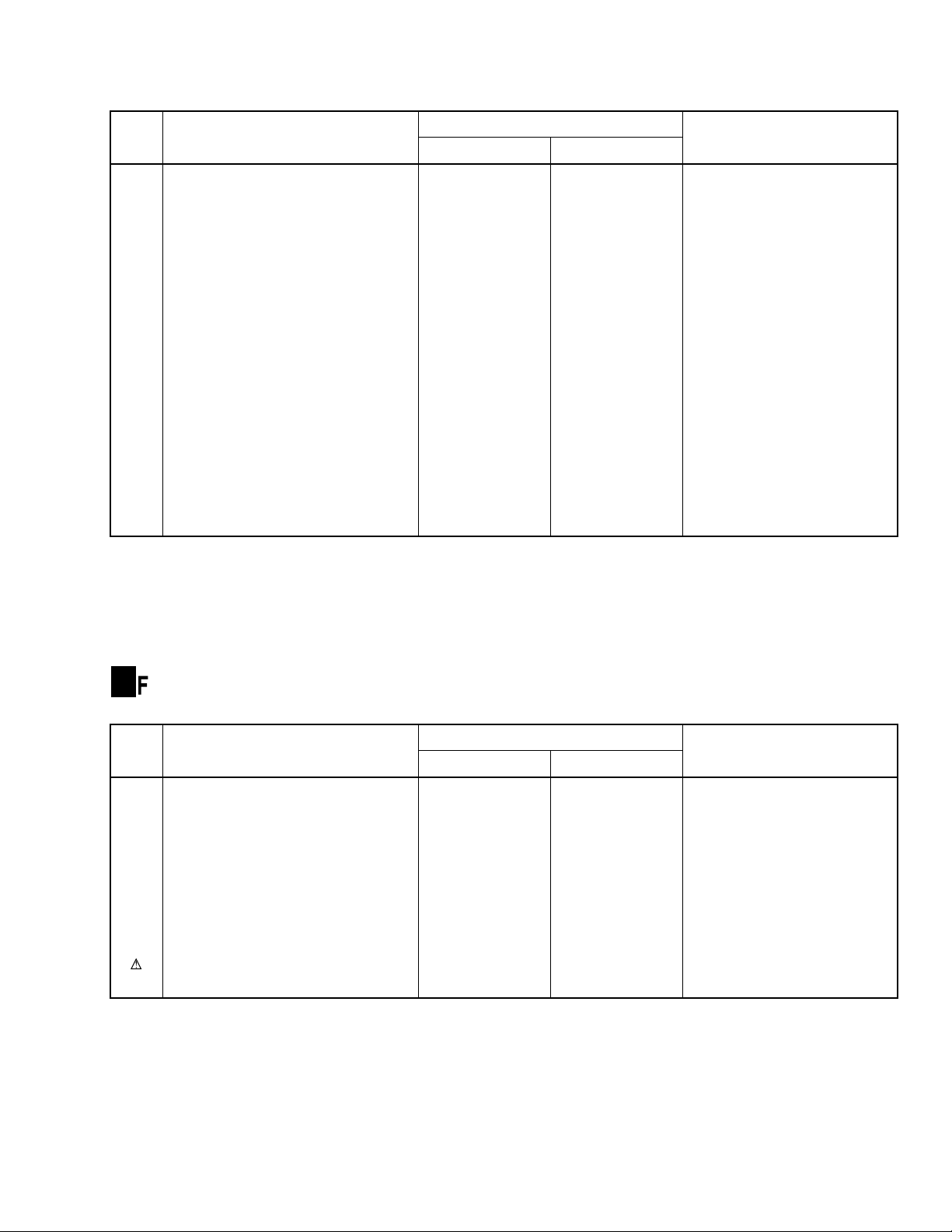
4.2 MAIN ASSY ADJUSTMENT
Note : Use disc : [ PAL DVD test disc ]
No. Adjustment Name
Master clock free-running adjustment
1
(Clock system adjustment)
2
Y level adjustment of CVBS system
(Output system adjustment)
C level adjustment of CVBS system
3
(Output system adjustment)
Y level adjustment of component system
4
(Output system adjustment)
PB level adjustment of component system
5
(Output system adjustment)
PR level adjustment of component system
6
(Output system adjustment)
It is recommended to adjust using PAL Disc.
Adj. Point Measurement Point
VC3001
VR7002
VR7001
VR7003
VR7004
VR7005
MAIN ASSY
IC4007 Pin54 (CLKO)
(M65774AFP)
Y output of S terminal
(75Ω termination)
C output of S terminal
(75Ω termination)
MAIN ASSY
CN7001 Pin11
(Y(G) Out)
MAIN ASSY
CN7001 Pin13
B
(P
MAIN ASSY
CN7001 Pin15
R
(P
(B) Out)
(R) Out)
Adjustment Value
27.000000MHZ
± 130Hz
1.0Vp-p ± 40mV
300mVp-p ± 12mV
760mVp-p ± 22mV
520mVp-p ± 15mV
520mVp-p ± 15mV
DVR-7000
Adjustment State
No input signal or during test disc playback
Playback the PAL DVD test disc(100%
color-bar). Terminate the Y output of S terminal with 75Ω and adjust so that the level
of between sync tip and white peak
becomes 1.0Vp-p.
Playback the PAL DVD test disc(100%color-
Terminate the C output of S terminal
bar).
with 75Ω and adjust so that the amplitude of
color burst becomes 300mVp-p.
Playback the PAL DVD test disc(100%
color-bar). At the pin 11 of CN7001 in the
MAIN ASSY, adjust so that the level of
between sync tip and white peak becomes
760mVp-p.
Playback the PAL DVD test disc(100%colorbar).
At the pin 13 of CN7001 in the MAIN
ASSY, adjust so that the level of between
bottom and top becomes 520mVp-p in the
100% color-bar screen.
Playback the PAL DVD test disc(100%color-
At the pin 15 of CN7001 in the MAIN
bar).
ASSY, adjust so that the level of between
bottom and top becomes 520mVp-p in the
100% color-bar screen.
When NTSC test disc GGV1025 is used, the adjustment No.2 to No.6 value is changed to the following value.
No. Adjustment Name
2
Y level adjustment of CVBS system
(Output system adjustment)
C level adjustment of CVBS system
3
(Output system adjustment)
Y level adjustment of component system
4
(Output system adjustment)
PB level adjustment of component system
5
(Output system adjustment)
PR level adjustment of component system
6
(Output system adjustment)
Adj. Point Measurement Point
VR7002
VR7001
VR7003
VR7004
VR7005
Y output of S terminal
(75Ω termination)
C output of S terminal
(75Ω termination)
MAIN ASSY
CN7001 Pin11
(Y(G) Out)
MAIN ASSY
CN7001 Pin13
B
(P
MAIN ASSY
CN7001 Pin15
R
(P
(B) Out)
(R) Out)
Adjustment Value
980mVp-p ± 39mV
280mVp-p ± 11mV
745mVp-p ± 22mV
390mVp-p ± 12mV
390mVp-p ± 12mV
Adjustment State
Playback the NTSC DVD test disc (75%
color-bar). Terminate the Y output of S terminal with 75Ω and adjust so that the level
of between sync tip and white peak
becomes 980mVp-p.
Playback the NTSC DVD test disc(75%colorbar).
Terminate the C output of S terminal
with 75Ω and adjust so that the amplitude of
color burst becomes 280mVp-p.
Playback the NTSC DVD test disc (75%
color-bar). At the pin 11 of CN7001 in the
MAIN ASSY, adjust so that the level of
between sync tip and white peak becomes
745mVp-p.
Playback the NTSC DVD test disc(75%colorbar).
At the pin 13 of CN7001 in the MAIN
ASSY, adjust so that the level of between
bottom and top becomes 390mVp-p in the
75% color-bar screen.
Playback the NTSC DVD test disc (75%
color- bar).
MAIN ASSY, adjust so that the level of between bottom and top becomes 390mVp-p
in the 75% color-bar screen.
At the pin 15 of CN7001 in the
Note : Do the MAIN ASSY adjustment first, before TUMJ ASSY adjustment.
When using 75% color bar, adjust making P
B/PR
output to 75%.
45
Page 46

DVR-7000
E
MAIN ASSY
F
VR7004
VR7005
VR7002 VR7001
IC4007
VC3001
1 22
VR7003
54
SIDE A
CN7001
46
Fig.2 Adjustment Point
Page 47

DVR-7000
5. GENERAL INFORMATION
5.1 MODEL TYPE AND REGION SETTING
Setting the Model type and Region No. for DVD Recorder
For the DVD recorder DVR-7000/WL/RD , it is necessary to set the region No. [ 4 ] on the FLASH ROM in the MAIN ASSY
and the model type [WL] on the EEPROM in the TUMJ ASSY. So when the MAIN ASSY or TUMJ ASSY is renewed,
"The Model type and Region setting mode screen" is displayed automatically.
(Note : WL/RD type TUMJ ASSY is common with WL type TUMJ ASSY.)
Note : If the region No. is once set, it is unable to rewrite it. When it is necessary to change the region No., renew the MAIN
ASSY. And it is able to rewrite the once set model type on the EEPROM in the TUMJ ASSY only when the MAIN AS SY is renewed and setting the new region No. on the FLASH ROM.
How to set the Model type and Region No.
1. Turn the power on.
2. The setting request screen is displayed when the model type and region No. is not set.
At this time FL displays " MODE SETTING".
/WL/RD
[ Recorder's Model and Region Setting]
Please pick out any one of the following.
Button No. Model Region
[ 3 : WL_MODEL<Hong Kong> Region 3 ]
[ 4 : WL/RD_MODEL<Australia> Region 4 ]
3. Enter the data according to the mode menu by the service remote control unit.
4. The recorder restarts automatically.
5. Set the shipping position. (stop + power off)
But it is omitted when making the Down Load of the system µ-com is done after this.
6. Turn off the power, then turn on the power again.
When the FL displays "MODEL MISMATCH" after connecting the AC plug to the outlet.
It displays, connecting the AC plug to the outlet when the setting is mismatched between the software setting of the model
type data on the EEPROM and the µ-com hardware pin setting of the model type in the TUMJ ASSY.
At this time, it is unable to turn on the power.
↓
It is considered the TUMJ PCB board fault (model type hardware pin setting fault).
Note :
Pin 76=Region 1, Pin 77=Region 2, Pin 98=Region 3
Check the corresponded pin according to the right table.
[Tuner control µ-com hardware pin setting of the model type]
L : Pull down
H : Pull up
[Tuner µ-com Hardware Pin Setting Table]
Pin76 Pin77 Pin98
WL/RD type H H L
WL type H H L
WY, WV type L H L
When the screen shows the following display after turning on the power
<display 1>
It displays, exchanging the MAIN ASSY or TUMJ ASSY,etc when the combination of model type and region No. already set
is mismatched.
After this, it is unable to operate any functions.
↓
Match the combination between the model type and region No. setting, or renew the ASSY and set the data newly.
< Model and Region don't match >
Model [already memorized on the TUFL-EEPROM] : WL_MODEL
Region [already memorized on the MAIN-CPU-FLASH ROM] : 2
Please take the power-plug off
the plug socket
model type information in the TUMJ ASSY
region information memorized in the MAIN ASSY
[When WY type MAIN Board is mounted to the WL/RD type model.]
Note : WL/RD type TUMJ ASSY is common with WL type model.
Only the WL/RD type MAIN ASSY region setting is different.
When the screen shows the following display after setting the Model type and Region No.
<display 2>
It displays, renewing TUMJ ASSY,etc when setting the different model type from the region No. already set in the FLASH
ROM in the MAIN ASSY.
↓
Match the combination between the model type and region No. setting, or renew the MAIN ASSY and set the data newly.
< You can't change and overwrite the Region No. ! >
Region was already memorized on the MAIN-CPU-FLASHROM
and you can't overwrite the different Region.
Region[already memorized on the MAIN-CPU-FLASHROM] : 4
Model-Region[that you selected just now] : WY_MODEL -2
Please take the power-plug off
the plug socket.
region information memorized in the MAIN ASSY
region information selected by the key input
at the setting mode screen
[When WY type TUMJ Board is is paired to the WL/RD type
MAIN Board.]
47
Page 48

DVR-7000
5.2 IC
• The information shown in the list is basic information and may not correspond exactly to that shown in the schematic diagrams.
List of IC
•
PE5322C9, MSP3417G, LC749793JM, TB1274AF, MM1394AF
PE5322C9 (TUJB ASSY : IC2003)
• Tuner Control Microcomputer
Pin Function (1/2)
•
.oNkraMemaNniPO/InoitcnuFniP.oNkraMemaNniPO/InoitcnuFniP
1021PREMITO remitrofDEL1412P1DXTO
2121PDELDVDODELDVD24
3221PFFOLFOFFOLFroF3432PQERUTO
4321PYBLODO YBLODLFrofDEL4442PTRPTRWO noissimrepgnitirwMORPEE
5421PSCLFO enilnoitacinummocrevirDLF5452PMADSO/Ituptuo/tupniatadC2I
6
521PTSRLFX
7
621PAGOJ
8721PBGOJI tupniGOJLF8408PQYBTSO edomybdnatsxelpitlumedoiduA
9DDVDDV
012X2X
111X1X1538PNO_PO langisNOREWOP
21V
SS
V
SS
312TX2TX
41
1TX1TX
51TESERXNITESERXI tupniCIteseR5578P1LESUT
6100PKCAUTI enilnoitacinummocNIAM65
7110PARTNIX
8120PBRTNIX8524PSBVCXO tcelesetisopmocS
9130PCN
0240PCN
1250PIKNILNI tupniatadKNILN1654P1LESNILO 1hctiwstupnilanretxE
2260PCN
32ddVAddVA
420feRVAfeRD/AI tupniegatlovecnereferD/A46
5201P1YEK
6211P2YEK2tupniYEKLF6625PCN
7221P
8231P8645PNOUTONOrenuT
9241PNOITCNUFI )YBTS(tupninoitcnuftracS9655PKNALBI langisgniknalBtracS
0351PTFAI tupnipaggninutevawdnuorG0765PEZEEQSO
1361POMREHTI tupninoitcetederutarepmeT1775PS_TELO lanimretSroflangisRETTEL
23
71PCN
SSV
33A
43031PNO_IVO tupniENILrofNOtiucricoediV4716PCN
53131PLTCTSRO
631feRVAfeRA/DI tupniegatlovecnereferA/D6736P1NOIGER
7307P7746P2NOIGER2noigeR
8317PATADLF
9327PPCLF9766PTSRLBXO langisteserretsarB
0402P1DXRI enilnoitacinummocNIAM0876PSCLESXI
CN
A
SSV
OlangisteserEVIRDLF6462PTESERXOTUOTESER
ItupniGOJLF7472PMLCSO tupnikcolcC2I
−
IkcolareczHM6atcennoC
−
Itupnik23
InoitacinummocCTR
−
CN9534PGNHCSO ledomLAProflangistcelestupni-S
−
CN0644PL4XO LAProfnoitarapesC/Yenil-4
−
CN2664P2LESNILO 2hctiwstupnilanretxE
−
I
−
CN
−
CN27V
−
OenilnoitacinummocREVIRDLF
ylppusrewoP9418PIVADXI ydaersiatadCDPnehw"L"
dnuorG2548PLAPXO MACES:H,LAP:L
ylppusrewoP3674PNO_FO nafroflangisFFO/NO
1tupniYEKLF5615PECCSO elbanelellarap-lairesdaoBtracS
dnuorggolanA3706POKNILNO tracSroflangistuptuokniLN
gasroflangisetumteseR
serusaem
22P1KCSA
0528PCN
3558PLMACESXO 'LMACES:H,LMACES:L
4568PURHTVXO hguorhttracS:LtracS
04P2LESUT
75
14PEVAS_P
05PYSUB
7635PTEDNAFI noitcetednoitatorNAF
SS
5726PSCLBO retsarbroflangistcelespihC
8756PTSR1VAO langisteser1VA
V
SS
I
−
OSBroevawdnuorgehttceleS
OedomrewopevastracS
IlangisYSUBretsarB
−
−
−
I
CIlortnoc
CN
CN
tracSdna
dnuorG
CN
1noigeR
)UE(hctiws
enilnoitacinummocNIAM
renutfotseuqernoitacinummoC
lanimretDroflangisEZEEQS
langisSrof/noitcetedtupniSroF
48
Page 49

Pin Function (2/2)
Sound IF1
ADC
ADC Prescale
SCRAT1
Source Select
Loudspeaker
DAC
DAC
SCRAT
Output
Select
De-
modulator
SCRAT
DSP
Input
Select
Pre-
processing
Loud-
speaker
Sound
Processing
SCRAT1
MONO
•
.oNkraMemaNniPO/InoitcnuFniP.oNkraMemaNniPO/InoitcnuFniP
18DDVDDV
28
001P
38101P3973PRKEHCXI edomrekcehC
48201P49TSETPPVI HSALFroftupniPPV
58301P5909P1REKAMI 1edocnoitacifitnedierutcafunaM
6803P6919P1MIDLF
7813P7929P2MIDLF
8823P8939P3NOIGERI 3edocnoitanitseD
9833P9949P2REKAMI 2edocnoitacifitnedierutcafunaM
0943PCNYSSCI CERSCroftupniCNYSSC00159PECIVRSXI edomecivreS
−
ylppusrewoP1953PRILESI tupnilortnocetomeR
29
63P
OREMIDLFroF
DVR-7000
MSP3417G (TUJB ASSY : IC4702)
• Stereo Decoder IC
Block Diagram
•
49
Page 50

DVR-7000
Pin Function
•
.oNniP
PFQMP
nip-44
1PUSVAXylppusrewopgolanA
2+1NI_ANANIVL1tupniFI
3-NI_ANANIVLnommocFI
4NETSETNIXniptseT
5NI_LATXNIX rotallicsolatsyrC
6TUO_LATXTUOX rotallicsolatsyrC
7PTVLniptseT
81_O/I_RTC_DTUO/NIX 1_O/I_RTC_D
90_O/I_RTC_DTUO/NIX 0_O/I_RTC_D
01LES_RDANIX tcelessserddasuBC2I
11QYBDNATSNIX )evitca-wol(ybdnatS
21LC_C2ITUO/NIXkcolcCII
31AD_C2ITUO/NIXatadCII
41PTVLniptseT
51PTVLniptseT
61PTVLniptseT
71PTVLniptseT
81OP_CTTUOVL*niptseT
91PUSVDXV5+ylppusrewoplatigiD
02SSVDXdnuorglatigiD
12PTVLniptseT
22QTESERNIX teser-no-rewoP
32CNVLdetcennoctoN
42CNVLdetcennoctoN
522FERVXtrapegatlov-hgih2dnuorgecnerefeR
62R_MCADTUOVLthgir,tuorekaepsduoL
72L_MCADTUOVLtfel,tuorekaepsduoL
82CNVLdetcennoctoN
921FERVXtrapegatlov-hgih1dnuorgecnerefeR
03R_TUO_1CSTUOVLthgir,tuptuo1TARCS
13L_TUO_1CSTUOVLtfel,tuptuo1TARCS
23CNVLdetcennoctoN
33PUSVHAXV0.8+ylppusrewopgolanA
43M_LPACXNIAMroticapacemuloV
53SSVHAXdnuorggolanA
63CDNGAX trapega-tlov-hgihegatlovecnerefergolanA
73CNVLdetcennoctoN
83CNVLdetcennoctoN
93CNVLdetcennoctoN
04L_NI_1CSNIVLtfel,tupni1TARCS
14R_NI_1CSNIVLthgir,tupni1TARCS
24POTFERVXretrevnocD/AFIegatlovecnerefeR
34NI_ONOMNIVLtupnionoM
44SSVAXdnuorggolanA
emaNniPepyT
noitcennoC
)desutonti(
moitpircseD
50
Page 51

LC74793JM (TUJB ASSY : IC7001)
SDA
SCL
DAV
SYNIN
SEPC
SEP OUT
SEP IN
CTRL2
VDD1,2
VDD1,2
SYNCJDG C Pout
VCO in
VCOR
HOUT
VOUT XIN XOUT CTRL1
CDLR
Timing generator
AFC circuit (VCO)
Synchronous
identification
circuit
V
separation
circuit
Data loading circuit
Data latch
circuit
Interface
Synchronous
separation data
separation
circuit
RST
• VPS, PDC, Data Slicer IC
Block Diagram
•
DVR-7000
51
Page 52

DVR-7000
Pin Function
•
1ISSVnipdnuorGnipdnuorgDNG
2niartXniprotallicsOlatX
3tuolatXniprotallicsOlatX
41LRTCnoitallicsolatX
5-CN-
6ADS
7LCS
8GDJCNYS
9tuoH
.oNniP.oNniPemaNniPsnoitpircsednoitcuF
CII
snipO/IataD
CII
niptupnikcolC
suonorhcnyslanretxE
tuonoitacifitnedilangis
niptup
suonorhcnyslanoziroH
niptuptuolangis
dnarotallicsolatXfplatsyrcafonoitcennocrofniP
rocsf4(kcolclanretxeehtfotupnirofroroticapac
)csfrocsf2
dnarotallicsolatXfplatsyrcafonoitcennocrofniP
rocsf4(kcolclanretxeehtfotupnirofroroticapac
)csfrocsf2
tupnikcolclanretxeehtneewtebrevoegnahcfoniP
,noitallicsolatX="oL".edomnoitallisolatXdnaedom
tupnikcolclanretxe="iH"
nipO/IatadSPV/CDP
]00111110[sserddaetirWsubCII
]10111110[sserddadaeRsubCII
niptunikcolcatadSPV/CDP
subCII
tuohtiwrohtiwebotdeifitnedietatsehttuptuootniP
.langissuonorhcnyslanretxeeht
langissuonorhcnysehthtiwetatsaroftuptuo"iH"
"oL"=nipTSRnehwtuptuokcolcnoitallicsolatX
)dnammocehthtiwtesernehwtuptuotoN(
langissuonorhcnyslanozirohehttuptuootniP
012SSVnipdnuorG)OCVrofnipDNG(nipdnuorgDNG
11TUOPCtuptuopmupegrahC FPLtuptuopmupegrahcehtfonoitcennocroF
21NIOCV
31ROCV
41VADtuptuognidaolataD deifitnedisiatadSPV/CDPehtnehwtuptuo"oL"
512DDV)V5+(nipylppusrewoP )OCVrofylppusrewoP:V5+(nipylppusrewoP
61niNYS
71CPESniptuptuolevelecilSnipkcehclevelecilS
81TUOPES
91NIPES
02tuoV
122LRTCnipportnoctupniniPES
22RLDCniplortnocesahpkcolC retsiserlortnocesahpkcolcehtottcennocotniP
tupni
nip
niptupnitiucic
niptuptuolangis
niptupnilangis
niptuptuolangis
egatlovlortnocnoitallicsO
egatlovlortnocnoitallicsO
noitarapessuonorhcnyS
suonorhcnysetisopmoC
suonorhcnyslacitreV
suonorhcnyslacitreV
niptupniegatrovlortnocnoitallicsoOCV
lortnocegnarnoitallicsoOCVottcennocotniP
retsiser
suonorhcnysni-tliubehtfotupnilangisoediV
tiucricnoitarapes
ehtfolangissuonorhcnysetisopmocehttuptuootniP
tiucricnoitarapessuonorhcnysni-tliub
retfalangissuonorhcnyslacitrevehttupniotniP
.niptuoPESfolangistuptuoehtfonoitargetni
tuoPESneewtebtiucricgnitargetniehttcennoC
.gnisutonnehw1DDCotsihtxiF.snip
)"iH"2LRTChtiwevitceffE(
.lagnissuonorhcnyslacitrevehttuptuootniP
"oL"=nipTSRehtnehwtuptuokcolcOVC
)dnammocehthtiwtesernehwtuptuotoN(
silangisCNYSVehttonrorehtehwlortnocotniP
tupniniPESottupni
tupniCNYSV="oL"
)tiucricnoitarapesVni-tliuB(
tupniCNYSV="iH"
52
32TSRniptupniteseR
421DDV)V5+(nipylppusrewoP)ylppusrewoplatigid:V5+(nipylppusrewoP
)tupnisiseretsyH(
.detiaroprocnirotsiserpu-lluP.niptupnitesermetsyS
Page 53

TB1274AF (SECAM ASSY : IC3501)
39
40
41
42
43
44
45
46
47
48
1
2
3
4
5 6 7
8
9
10 11
12
13
14
15
16
17
18
19
20
21
22
23
24
25
26
2728
2930
31
3233
34
35
36
37
38
C3-IN
CVBS3/Y3-IN
ADDRESS
C2-IN
CVBS2/Y2-IN
COMB SYS
Fsc-OUT
AFC-FIL
C1-IN
CVBS1/Y1-IN
SYNC-IN
CVBS-OUT
Vs
COMB Y-IN
D-V
FORCED-S
D-GND
SCP
HS
Yvi-OUT
SYNC-Vcc
SCL
SDA
COMB C-IN/
DD
APC-FIL
YS3
(RGB1-In)
SYNC-GND
Cr1-IN
Cd1-IN
Y1-IN
Y-OUT
CLP-FIL
Cb-OUT
Cr-OUT
YS1
(YCbCr2-In)
G1-IN
R1-IN
Y/C-GND
Cr2-IN
Cb2-IN
Y2-IN
Y/C-Vcc
B2-IN
G2-IN
R2-IN
YS2/YM
(RGB2-in)
FIL
XTAL
B1-IN
VCXO
Isc
APC
Sub-
Color
1H DL
LPF
SW
(C-MUTE)
P/N
DEMO
BPF/
TOF
ACC
Y
C
CVBS/YC
Select
Color
System
Bell
SECAM
DEMO
Black
Adj
SECAM
ID
Chroma
ID
S Double
Trap
EQ
Y DL
Sub-
contrast
V C/D
V
SEPA
H
VCO
H C/D
AFC
Nolse
Dat
SYNC
SEPA
MASK
Clamp
Sharp-
ness
CLP
SW
SW
Offset1
DL
Halftone
LPF
AMP
Setup
SW
IIC Bus
Control
V
INTEG
Chroma
Trap
P/N ID
De-
emphasls
Base-
band SW
CW
Phase
Tlnl
SW
Cb/Cr
Y
Matrix
Clamp
Clamp
Clamp
Offset2
Matrix
• Video Decoder IC
Block Diagram
•
DVR-7000
53
Page 54

DVR-7000
Pin Function(1/2)
•
.oNniPemaNniPnoitcnuFLANGISTUO/NI
1NI-1Y/1SBVC.Cpmalcaivlangis1Yro2SBVCtupnI
2NI-CNYS.CpmalcaivangiscnystupnI
3TUO-SBVClangisC+YroSBVCroflanimrettuptuO
4sV
5NI-YBMOCCpmalcaivretlifbmocmorflangisYtupnI
6DDV-DkcolBDC-H/DC-V/SUB/SDDrofDDVV5CD
7S-DECROF/NI-CBMOCCpmalcaivretlifbmocmorflangisCtupnII
8DNG-DkcolBDC-H/DC-V/SUB/SDDrofDNG
9SH
01PCS
11TUO-ivY
21ccV-CNYSkcolbOCVH/CNYSrofCCVV5CD
31LCS.subCIIroflanimretLCS
41ADSsubCIIroflanimretADS
51
61DNG-CNYSkcolbDCVH/CNYSrofDNG
71NI-1rCCpmalcaivlangis1rC/1bC/2YtupnI
81NI-1bCCpmalcaivlangis1rC/1bC/2Ytupn
91
02LIF-PLCretlifpmalc-YtcennoCCD
12TUO-YlangisrC/bC/YtuptuO
22TUO-bClangisrC/bC/YtuptuO
32TUO-rClangisrC/bC/YtuptuO
42)ni-2rCbCY(1SY
3SY
)ni-1BGR(
NI-1Y
hgoHevitcA
hsiHevitcA
WS-oediVyb
langis
langistupni
.cnysHnwod_tnuoctuptuO
.CFA-HhtiwcnysHtuptuO
.eslupeltsacdnastuptuO
esluppmalchtiweslupKLB-H
detcelesnoitazinorhcnysroflangisYtuptuO
tupni1BGRdnalangisniamrofWSnoitceleS
Cpmalcaivlangis1rC/1bC/2Ytupn
2rCbCYdnalangisniamrofWSnoitceleS
p-pV1:SBVC
)cnyshtiw(p-pV1:Y
V8.1:CD
)cnyshtiw(p-pV1
V7.1:CD
)cnyshtiw(p-pV2
V6.0:CD
V2.5†hgiH†V7.4
V8.0†woL†V0
)cnyshtiw(p-pV1
V8.1:CD
)tsrub(p-pV3
V4.2:CD
V0.5†S-DECROF†V0.4
)V5.3:hT(
V6.4†hgiH†V8.3
V0.1†woL†0
CP
H-BLK
Low
V4.4†PC†V6.3
V4.2†KLB-H†V6
V8.0†woL†V0.0
)‰k5.7(rotsisernwod-lluphtiw
)cnyshtiw(p-pV1
V1.2:CD
V0.5†BGR†V0.1
)V7.0:hT(
)cnyshtiw(p-pV1:Y
V7.1:CD
)rabroloc%001(p-pV7.0:rC/bC
V5.2:CD
)cnyshtiw(p-pV1:Y
V7.1:CD
)rabroloc%001(p-pV7.0:rC/bC
V5.2:CD
)cnyshtiw(p-pV1:Y
V7.1:CD
)rabroloc%001(p-pV7.0:rC/bC
V5.2:CD
CD
V8.1:rC/bCV3.1:Y
CA
p-pV7.0:Y
)cnys-non,Bd0(
)Bd0(p-pV7.0.dC/dC
lortnocesahpkcolcehtottcennocotniP
retsiser
rotsiserpu-lluP.niptupnitesermetsyS
.detiaroprocni
)tupnisiseretsyH(
V0.5†2rCbCY†V0.1
)V7.0:hT(
54
Page 55

Pin Function(2/2)
•
.oNniPemaNniPnoitcnuFLANGISTUO/NI
DVR-7000
52NI-1BCpmalcaivlangis1BGRtupnI
62NI-1GCpmalcaivlangis1BGRtupnI
72NI-1RCpmalcaivlangis1BGRtupnI
82DNG-C/YLDH1/WS-oediV/txeT/C/YrofDNG
92NI-2rCCpmalcaivlangis2rC/2bC/2YtupnI
03NI-2bCCpmalcaivlangis2rC/2bC/2YtupnI
13NI-2YCpmalcaivlangis2rC/2bC/2YtupnI
23ccV-C/YLDH1/WS-oediV/txeT/C/YrofccVV5CD
33NI-2BCpmalcaivlangis2BGRtupnI
43NI-2GCpmalcaivlangis2BGRtupnI
53NI-2RCpmalcaivlangis2BGRtupnI
63)ni-2BGR(MY/2SY
langis
tupni2BGRdnalangisniamrofWSnoitceleS
73LIFccV:C/Y:tennoC
83LATX
latX
zHM2.61tennoC
93NI-3CCpmalcaivlangisamorhctupnI
04LIF-CPA.noitaludomedamorhcrofretliftcennoC
14NI-3Y/3SBVCCpmalcaivlangis3Yro3SBVCtupnI
24SSERDA.sserddaevalsteS
34NI-2CCpmalcaivleangisamorhctupnI
44NI-2Y/2SBVCCpmalcaivlangis2Yro2SBVCtupnI
SYSBMOC
COLOR
SYSTEM
M-PAL
54
4.43PAL
SECAM
B/W
3.58/4.43
NTSC
N-PAL
PLUG
PLUG
45
46
LOW LOW
High LOW
LOW High
High High
64niPdnanip
sihtmorftlusernoitcnitsidmetsysroloctuptuO
64TUO-csFreirracbustuptuO
74LIF-CFAnoitcetedCFArofretliftcennoC
84NI-1CCpmalcaivlangisamorhctupnI
p-pV7.0
V5.2:CD
p-pV7.0
V5.2:CD
p-pV7.0
V5.2:CD
V7.1:CD
V5.2:CD
V7.1:CD
V5.2:CD
V7.1:CD
V5.2:CD
p-pV:7.0
V5.2:CD
p-pV:7.0
V5.2:CD
p-pV:7.0
V5.2:CD
p-pV3.0
V6.1:CD
V8.1:CD
V6.1:CD
V8.1:CD
5V
(3.1V)
V6.1:CD
)V7.0:hT(
V0.5†2rCbCY†V0.1
)cnyshtiw(p-pV1:Y
p-pV7.0:rC/bC
)rabroloc%001(
)cnyshtiw(p-pV1:Y
p-pV7.0:rC/bC
)rabroloc%001(
)cnyshtiw(p-pV1:Y
p-pV7.0:rC/bC
)rabroloc%001(
V5.1†MY†V0.1
V0.5†2BGR†V5.2
)V0.2:2hT,V7.0:1hT(
evawzHM2.61
p-pV1:SBVC
)cnyshtiw(p-pV1:Y
V3.1†H98/M88
HF8/HE8†V9.3
)V2.3:2hT,V5.1:1hT(
)tsrub(p-pV3.0
p-pV1:SBVC
)cnyshtiw(p-pV1:Y
High
0V
Low
p-pV48.0:CA
woleberugifehtninwohssa:CD
High
(2.1V)
Low
)tsrub(p-pV3.0
55
Page 56

DVR-7000
MM1394AF (SECAM ASSY : IC3601)
• NTSC/PAL Encoder IC
Block Diagram
•
Pin Function
•
.oNNIPEMANNIPNOITCNUF
11DNG
2
3
4
5tuolat'X.niptuptuotiucricrotallicsO
6nilat'X.niptupnireirracbuS
7LAP/CSTN
8
9
01niCNYS.niptupnilangiscnysetisopmoC
11CN.nipnepO
211ccV
31ferI
41ferV
51
61
71FFO/NOtuoOEDIV
810f
912ccV.ylppusrewopegatstuptuO
02tuoOEDIV
12
22
32
422DNG.DNGegatstuptuO
niY-R
niY-B
niS+Y
CN.nipnepO
CN.nipnepO
tuoR
tuoG
tuoB
56
p-pV00.1Y-R
:egatlovtupnimumixaM.sniptupnI
p-pV72.1Y-B
p-pV00.1Y-R
)p-pV882.0siCNYS(
V2.2sipmalcroflevelCD
nipgnittesedoM
CCV:CSTN
LAP:LAP
.tnerrucecnereferlanretnistesnipsihT
.DNGdnanipsihtneewtebrotsiserk74atcennoC
.nipegatlovecnereferlanretnI
V4:egatovecnerefeR
.DNGdnanipsihtneewtebroticapacFµ01atcennoC
FFO/NOtuptuoOEDIVsnrutnipsihT
DNG:NOtuptuoOEDIV
CCV:FFOtuptuoOEDIV
.stiucricyaleddnaretlifrof0fstesnipsihT
k02:CSTN
k61:LAP
.niptuptuolangisoedivetisopmoC
.daol57evirdnacCIsihT
.niptuptuolangisBGR
Page 57

6. PANEL FACILITIES AND SPECIFICATIONS
6.1 PANEL FACILITIES
REAR PANEL
DVR-7000
1 2 3 4 5 6 7
AC IN
COMPONENT
VIDEO OUT
Y
P
B
P
R
L
R
12 1
OUTPUT INPUT
2
/AUTO REC
S-VIDEO
VIDEO
AUDIO
OPTICAL COAXIAL IN
DIGITAL OUT CONTROL
11 10
1 AC IN – Power inlet
2 COMPONENT VIDEO OUT
For connecting to a TV or monitor that has
component video input
3 S-VIDEO OUTPUT 1, 2
For connecting to a TV, monitor, AV receiver or
other equipment with S-Video input
7 CONTROL IN / OUT
Use for connecting to other Pioneer components
bearing the Pioneer Î mark. Connect the
CONTROL OUT of one component to the
CONTROL IN of another using a mini-plug cord.
The device at the beginning of the chain acts as
the remote control sensor for everything in the
chain.
8
ANTENNA
IN
OUT
OUT
9
4 S-VIDEO INPUT 1, 2
For recording from a camcorder, VCR or other
equipment with S-Video output
5 DIGITAL OUT OPTICAL
For connecting to an AV receiver, Dolby Digital/
DTS/MPEG decoder or other equipment with
optical digital input
6 DIGITAL OUT COAXIAL
For connecting to an AV receiver, Dolby Digital/
DTS/MPEG decoder or other equipment with
coaxial digital input
8 ANTENNA IN
Connect the TV antenna here.
9 ANTENNA OUT
Press the signal from the ANTENNA IN terminal
to your TV.
10 AUDIO/VIDEO INPUT 1, 2/AUTO REC
For recording from a camcorder, VCR, satellite
receiver or other equipment
13 AUDIO/VIDEO OUTPUT 1, 2
For connecting to the audio and video inputs of a
TV, monitor, AV receiver or other equipment
57
Page 58

DVR-7000
REMOTE CONTROL
STANDBY
/ON
PLAYLIST
ERASE
G-code
CHP
MARK
PAUSE CM SKIP RETURN
8
REC PLAY STOP
PREV NEXT CHANNEL
¢4
MODE
DISCNAVI
ENTER
CM
REC
OPEN
/CLOSE
NAVI
MARK
SEARCH
MODE
JOG MODE
SETUP
EDIT
INPUT
SELECT
CLEAR
C321
G-code
Press, then use the number buttons to enter a G-code
programming number for timer recording.
58
654
PROGRAM
REPEAT ANGLE
TV
INPUT SELECT
TV VOLUME AUDIO SUBTITLE
TV CHANNEL MENU
A-B
SHIFT
S
DISPLAY
TOP MENU
0987
Î
Page 59

6.2 SPECIFICATIONS
DVR-7000
General
System ................... DVD-Video, DVD-R/RW, Video-CD, CD
Power requirements.............................. 220-240 V, 50/60 Hz
Power consumption ....................................................... 60 W
Power consumption in standby mode ............ 1.5 W (FL off)
Weight .......................................................................... 7.0 kg
Dimensions .....................420 (W) x 10 7 ( H ) x 373.5 (D) mm
Operating temperature .................................. +5°C to +35°C
Operating humidity................. 5% to 85% (no condensation)
TV format ........................................ PAL/SECAM(tuner only)
Recording
Recording format ................................ DVD VideoRecording
DVD-VIDEO
Recordable discs ................................... DVD-ReRecordable
DVD-Recordable
Video recording format
Sampling frequency .................................................13.5MHz
Compression format ....................................................MPEG
Audio recording format
Sampling frequency ..................................................... 48kHz
Compression format ..........................................Dolby Digital
Recording time
DVD-RW (VR mode)
Standard (SP) .......................................... Approx. 2 hours
Manual rate (MN)................................. Approx. 1–6 hours
DVD-R/RW (Video mode)
V1 ............................................................... Approx. 1 hour
V2 ............................................................. Approx. 2 hours
Tuner
Receivable channels
Input/Output
ANTENNA input/output terminal...................... VHF/UHF set
Video input ...................................... Input 1,2 (rear), 3 (front)
Input level ................................................. 1.0 Vp-p (75 Ω)
Jacks .................................................................. RCA jack
Video output.......................................................... Output 1 ,2
Output level............................................... 1.0 Vp-p (75 Ω)
Jacks ................................................................... RCA jack
S-Video input .................................. Input 1,2 (rear), 3 (front)
Y (luminance) - Input level .......................... 1 Vp-p (75 Ω)
C (color) - Input level ............................ 300 mVp-p (75 Ω)
Jacks ............................................................
S-Video output ...................................................... O u t pu t 1 ,2
Y (luminance) - Output level........................ 1 Vp-p (75 Ω)
C (color) - Output level ......................... 300 mVp-p (75 Ω)
Jacks ............................................................
Component video output
Output level...........................................Y: 1.0 Vp-p (75 Ω)
Jacks ................................................................. RCA jacks
Audio input ............................... Input 1,2 (rear), 3 (front) L/R
Input level
During audio input ..................................................2V rms
(Input impedence: more than 22kΩ)
Jacks ................................................................. RCA jacks
Audio output................................................... Output 1,2 L/R
During audio output ................................................2V rm s
(Output impedence: less than 1.5kΩ)
Jacks ................................................................. RCA jacks
75 Ω (coaxial)
4 pin mini DIN
4 pin mini DIN
CB, CR: 0.7 Vp-p (75 Ω)
Timer
Programs............................................... 1 month/8 programs
Clock ............................ Quartz lock (24-hour digital display)
Power off memory...................................... Approx. 48 hours
SECAM L PAL B/G PAL I
Frequency
VHF (low)
VHF (high)
Hyper
UHF
STEREO
B/G - A2
I - NICAM
L - NICAM
B/G - NICAM
49 - 65 MHz
104 - 300 MHz
300 - 470 MHz
470 - 862 MHz
Channel
2 - 4
5 - 10
B - Q
S21 - S41
21 - 69
Frequency
47 - 89 MHz
104 - 300 MHz
302 - 470 MHz
470 - 862 MHz
Channel
E2 - E4
X - Z
E5 - E12
S1 - S20
M1 - M10
U1 - U10
S21 - S41
E21 - E69
Frequency
44 - 89 MHz
104 - 300 MHz
302 - 470 MHz
470 - 862 MHz
Channel
A - C
X - Z
D - J
11, 13
S1 - S20
S21 - S41
E21 - E69
59
Page 60

DVR-7000
Control i n p u t/ o u tp u t ..................................... Mini jack 1 each
DV input /o u t pu t ............... 4 p i n (i.LINK/IEEE 1394 standard)
Supplied accessories
Remote control..................................................................... 1
Dry cell batteries (AA/R6P) ................................................. 2
Stereo audio cable (red/white) ............................................ 1
Video cable (yellow)............................................................. 1
RF antenna cable ................................................................ 1
Power cable ......................................................................... 2
Operating Instructions ......................................................... 2
Note: The specifications and design of this product are
subject to change without notice, due to improvement.
ACCESSORIES
Remote Control
(VXX2777)
STANDBY
OPEN
/ON
/CLOSE
CHP
NAVI
PLAYLIST
SETUP
MARK
MARK
ERASE
EDIT
DISCNAVI
ENTER
JOG MODE
PAUSE CM SKIP RETURN
CM
8
REC PLAY STOP
PREV NEXT CHANNEL
¢4
REC
SEARCH
INPUT
G-code
MODE
MODE
SELECT
CLEAR
C321
654
A-B
PROGRAM
REPEAT ANGLE
0987
TV
INPUT SELECT
SHIFT DISPLAY
S
TV VOLUME AUDIO SUBTITLE
TOP MENU
TV CHANNEL MENU
Î
Stereo audio cable(L=1.5m)
(VDE1033)
white
red
Dry cell Batteries
(R6P,AA)
Video cable(L=1.5m)
(VDE1034)
yellow
RF antenna cable(L=1.5m)
(VDE1075)
AC power cord
(ADG1127)
(ADG1156)
60
 Loading...