

Page 1
PIONEER CORPORATION 4-1, Meguro 1-chome, Meguro-ku, Tokyo 153-8654, Japan
PIONEER ELECTRONICS (USA) INC. P.O. Box 1760, Long Beach, CA 90801-1760, U.S.A.
PIONEER EUROPE NV Haven 1087, Keetberglaan 1, 9120 Melsele, Belgium
PIONEER ELECTRONICS ASIACENTRE PTE. LTD. 253 Alexandra Road, #04-01, Singapore 159936
PIONEER CORPORATION 2005
÷ When servicing this model, some service procedures may reset the customer settings
to the factory default settings. Make sure to explain this to the customer.
An HDD (Hard Disc Drive) is mounted in this product.
The HDD is a precision instrument very vulnerable to shock and electrostatic charges. Please read
"7.3 Cautions on Handling the HDD" in this manual and exercise sufficient caution when handling the
HDD itself, as well as the product with the HDD built in.
When an HDD becomes defective and inoperable, restoration of the user's data recorded on the HDD,
or copying of the user's recorded data to other media (such as a new HDD) is totally impossible.
Before servicing, OBTAIN THE USER'S PRIOR CONSENT to that effect.
The user must be made aware that all recorded data are deleted if the HDD is intialized.
HDD/DVD
MENUTOP MENU
ENTER
HOME
STANDBY / ON
MENU
DVR-533H-S
ONE TOUCH
COPY
RETURN
REC
PULL - OPEN
ORDER NO.
RRV3173
DVD RECORDER
DVR-533H-S
DVR-633H-S
DVR-531H-S
THIS MANUAL IS APPLICABLE TO THE FOLLOWING MODEL(S) AND TYPE(S).
Serial No.
Model Type Power Requirement Region No.
DVR-533H-S KUXV AC120V 1 &&DL######$$
DVR-533H-S KCXV AC120V 1 &&DL######$$
DVR-633H-S KUXV/CA AC120V 1 &&DL######$$
DVR-531H-S KUXV/CA AC120V 1 &&DL######$$
DVR-531H-S KCXV AC120V 1 &&DL######$$
Please confirm 3rd & 4th
alphabetical letters.
For details, refer to "Important Check Points for Good Servicing" .
T-ZZV JUNE 2005 printed in Japan
Page 2
1234
SAFETY INFORMATION
A
This service manual is intended for qualified service technicians; it is not meant for the casual
do-it-yourselfer. Qualified technicians have the necessary test equipment and tools, and have been
trained to properly and safely repair complex products such as those covered by this manual.
Improperly performed repairs can adversely affect the safety and reliability of the product and may
void the warranty. If you are not qualified to perform the repair of this product properly and safely, you
should not risk trying to do so and refer the repair to a qualified service technician.
WARNING
This product contains lead in solder and certain electrical parts contain chemicals which are known to the state of California to
B
cause cancer, birth defects or other reproductive harm.
Health & Safety Code Section 25249.6 – Proposition 65
NOTICE
(FOR CANADIAN MODEL ONLY)
Fuse symbols (fast operating fuse) and/or (slow operating fuse) on PCB indicate that replacement
parts must be of identical designation.
REMARQUE
(POUR MODÈLE CANADIEN SEULEMENT)
Les symboles de fusible (fusible de type rapide) et/ou (fusible de type lent) sur CCI indiquent que
C
les pièces de remplacement doivent avoir la même désignation.
(FOR USA MODEL ONLY)
1. SAFETY PRECAUTIONS
The following check should be performed for the
continued protection of the customer and service
technician.
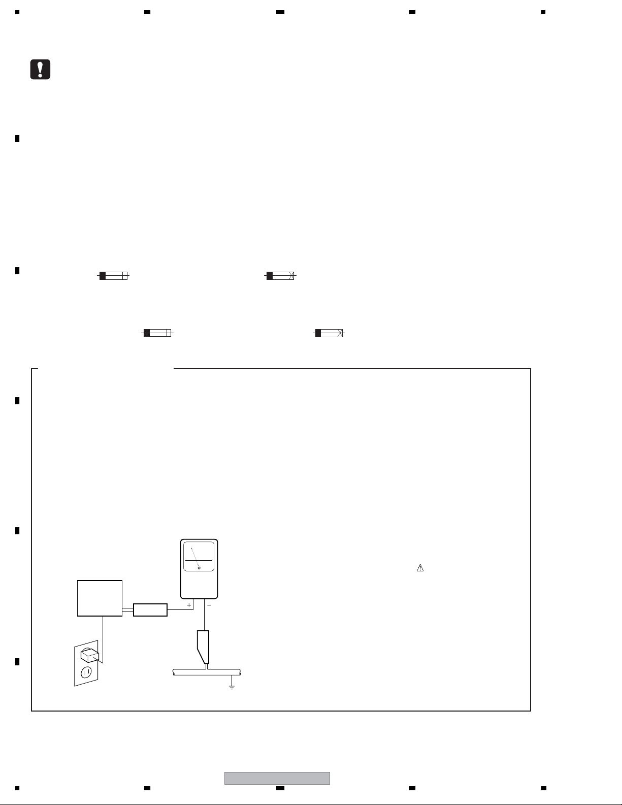
LEAKAGE CURRENT CHECK
Measure leakage current to a known earth ground
(water pipe, conduit, etc.) by connecting a leakage
current tester such as Simpson Model 229-2 or
D
equivalent between the earth ground and all exposed
metal parts of the appliance (input/output terminals,
screwheads, metal overlays, control shaft, etc.). Plug
the AC line cord of the appliance directly into a 120V
AC 60 Hz outlet and turn the AC power switch on. Any
current measured must not exceed 0.5 mA.
Leakage
current
E
Device
under
test
Also test with
plug reversed
(Using AC adapter
plug as required)
Test all
exposed metal
surfaces
AC Leakage Test
tester
Reading should
not be above
0.5 mA
Earth
ground
ANY MEASUREMENTS NOT WITHIN THE
LIMITS OUTLINED ABOVE ARE INDICATIVE
OF A POTENTIAL SHOCK HAZARD AND
MUST BE CORRECTED BEFORE RETURNING THE APPLIANCE TO THE CUSTOMER.
2. PRODUCT SAFETY NOTICE
Many electrical and mechanical parts in the appliance
have special safety related characteristics. These are
often not evident from visual inspection nor the
protection afforded by them necessarily can be obtained
by using replacement components rated for voltage,
wattage, etc. Replacement parts which have these
special safety characteristics are identified in this
Service Manual.
Electrical components having such features are
identified by marking with a
on the parts list in this Service Manual.
The use of a substitute replacement component which
does not have the same safety characteristics as the
PIONEER recommended replacement one, shown in the
parts list in this Service Manual, may create shock, fire,
or other hazards.
Product Safety is continuously under review and new
instructions are issued from time to time. For the latest
information, always consult the current PIONEER
Service Manual. A subscription to, or additional copies
of, PIONEER Service Manual may be obtained at a
nominal charge from PIONEER.
on the schematics and
F
2
1234
DVR-533H-S
Page 3
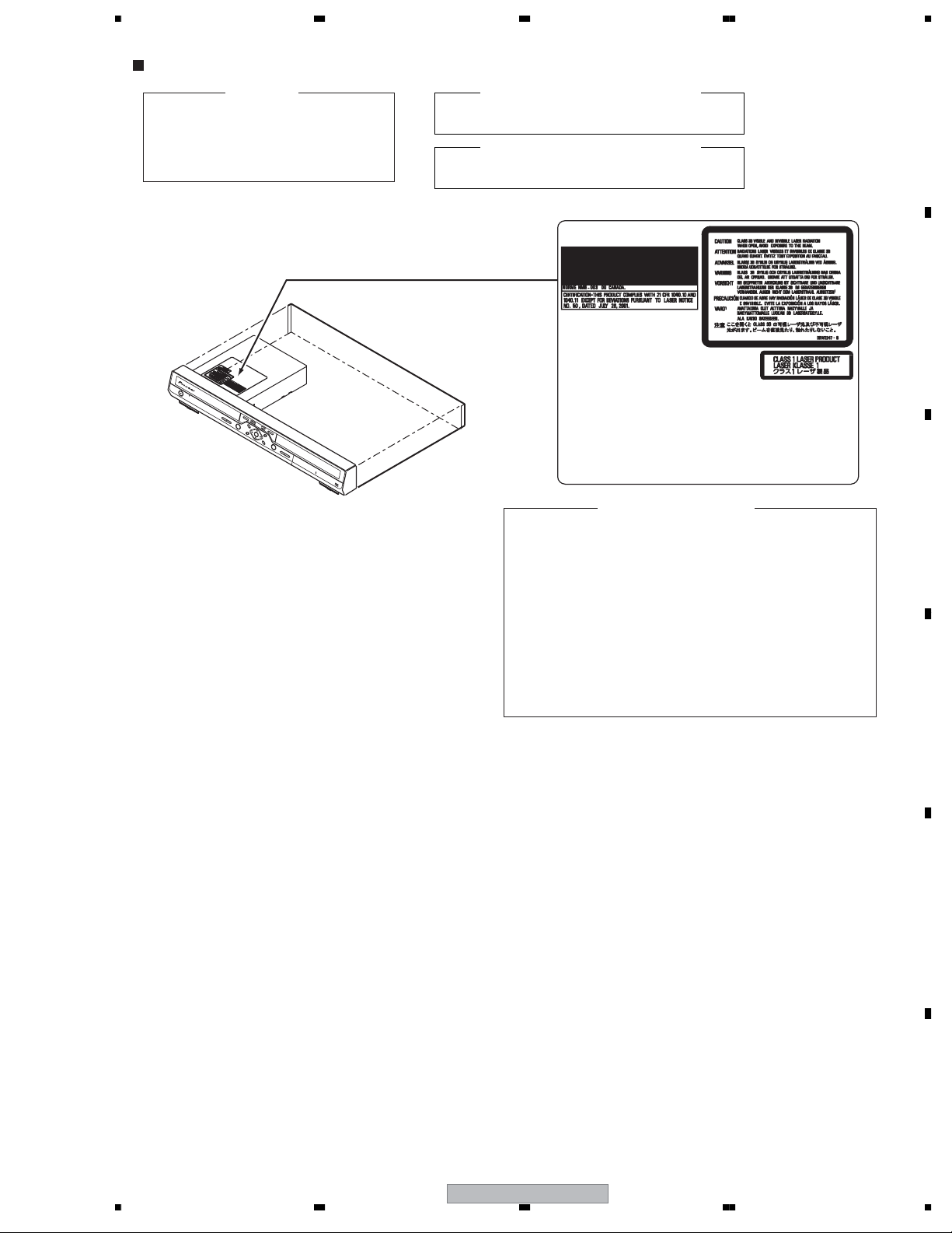
5678
LABEL CHECK
IMPORTANT
THIS PIONEER APPARATUS CONTAINS
LASER OF CLASS 1.
SERVICING OPERATION OF THE APPARATUS
SHOULD BE DONE BY A SPECIALLY
INSTRUCTED PERSON.
S
T
A
N
D
B
Y
/
O
N
T
O
P
M
E
N
U
HOME
M
H
D
ENU
D
/
D
V
D
M
E
E
N
N
U
T
E
R
R
E
T
U
R
N
R
E
C
O
N
E
T
O
C
U
O
C
P
H
Y
P
U
L
L
O
P
E
N
MAXIMUM OUTPUT POWER: 100 mW
LASER DIODE CHARACTERISTICS
WAVELENGTH: 654 - 662 nm
LASER DIODE CHARACTERISTICS
MAXIMUM OUTPUT POWER: 5 mW
WAVELENGTH: 770 - 810 nm
A
B
DRW2247
Additional Laser Caution
C
1. The ON/OFF(ON:low level,OFF:high level) status of the
CLAMP signals for detecting the loading state are detected
by the drive CPUs, and the design prevents laser diode
oscillation when the CLAMP signal turns OFF.
In normal operation, if no disc is clamped, the laser diode
oscillation is disabled.
However, the interlock does not always operate in the test
mode.
2. When the cover is opened, close viewing of the objective
lens with the naked eye will cause exposure to a Class 3A
laser beam.
D
E
56
DVR-533H-S
F
3
7
8
Page 4
1234
[Important Check Points for Good Servicing]
In this manual, procedures that must be performed during repairs are marked with the below symbol.
Please be sure to confirm and follow these procedures.
A
1. Product safety
Please conform to product regulations (such as safety and radiation regulations), and maintain a safe servicing environment by
following the safety instructions described in this manual.
1 Use specified parts for repair.
Use genuine parts. Be sure to use important parts for safety.
2 Do not perform modifications without proper instructions.
Please follow the specified safety methods when modification(addition/change of parts) is required due to interferences such as
radio/TV interference and foreign noise.
B
C
D
3 Make sure the soldering of repaired locations is properly performed.
When you solder while repairing, please be sure that there are no cold solder and other debris.
Soldering should be finished with the proper quantity. (Refer to the example)
4 Make sure the screws are tightly fastened.
Please be sure that all screws are fastened, and that there are no loose screws.
5 Make sure each connectors are correctly inserted.
Please be sure that all connectors are inserted, and that there are no imperfect insertion.
6 Make sure the wiring cables are set to their original state.
Please replace the wiring and cables to the original state after repairs.
In addition, be sure that there are no pinched wires, etc.
7 Make sure screws and soldering scraps do not remain inside the product.
Please check that neither solder debris nor screws remain inside the product.
8 There should be no semi-broken wires, scratches, melting, etc. on the coating of the power cord.
Damaged power cords may lead to fire accidents, so please be sure that there are no damages.
If you find a damaged power cord, please exchange it with a suitable one.
9 There should be no spark traces or similar marks on the power plug.
When spark traces or similar marks are found on the power supply plug, please check the connection and advise on secure
connections and suitable usage. Please exchange the power cord if necessary.
0 Safe environment should be secured during servicing.
When you perform repairs, please pay attention to static electricity, furniture, household articles, etc. in order to prevent injuries.
Please pay attention to your surroundings and repair safely.
2. Adjustments
To keep the original performance of the products, optimum adjustments and confirmation of characteristics within specification.
Adjustments should be performed in accordance with the procedures/instructions described in this manual.
3. Lubricants, Glues, and Replacement parts
Use grease and adhesives that are equal to the specified substance.
E
Make sure the proper amount is applied.
4. Cleaning
For parts that require cleaning, such as optical pickups, tape deck heads, lenses and mirrors used in projection monitors, proper
cleaning should be performed to restore their performances.
5. Shipping mode and Shipping screws
To protect products from damages or failures during transit, the shipping mode should be set or the shipping screws should be
installed before shipment. Please be sure to follow this method especially if it is specified in this manual.
F
4
1234
DVR-533H-S
Page 5

5678
CONTENTS
SAFETY INFORMATION......................................................................................................................................2
1. SPECIFICATIONS.............................................................................................................................................6
2. EXPLODED VIEWS AND PARTS LIST.............................................................................................................8
2.1 PACKING....................................................................................................................................................8
2.2 EXTERIOR SECTION ..............................................................................................................................10
2.3 FRONT PANEL SECTION ........................................................................................................................12
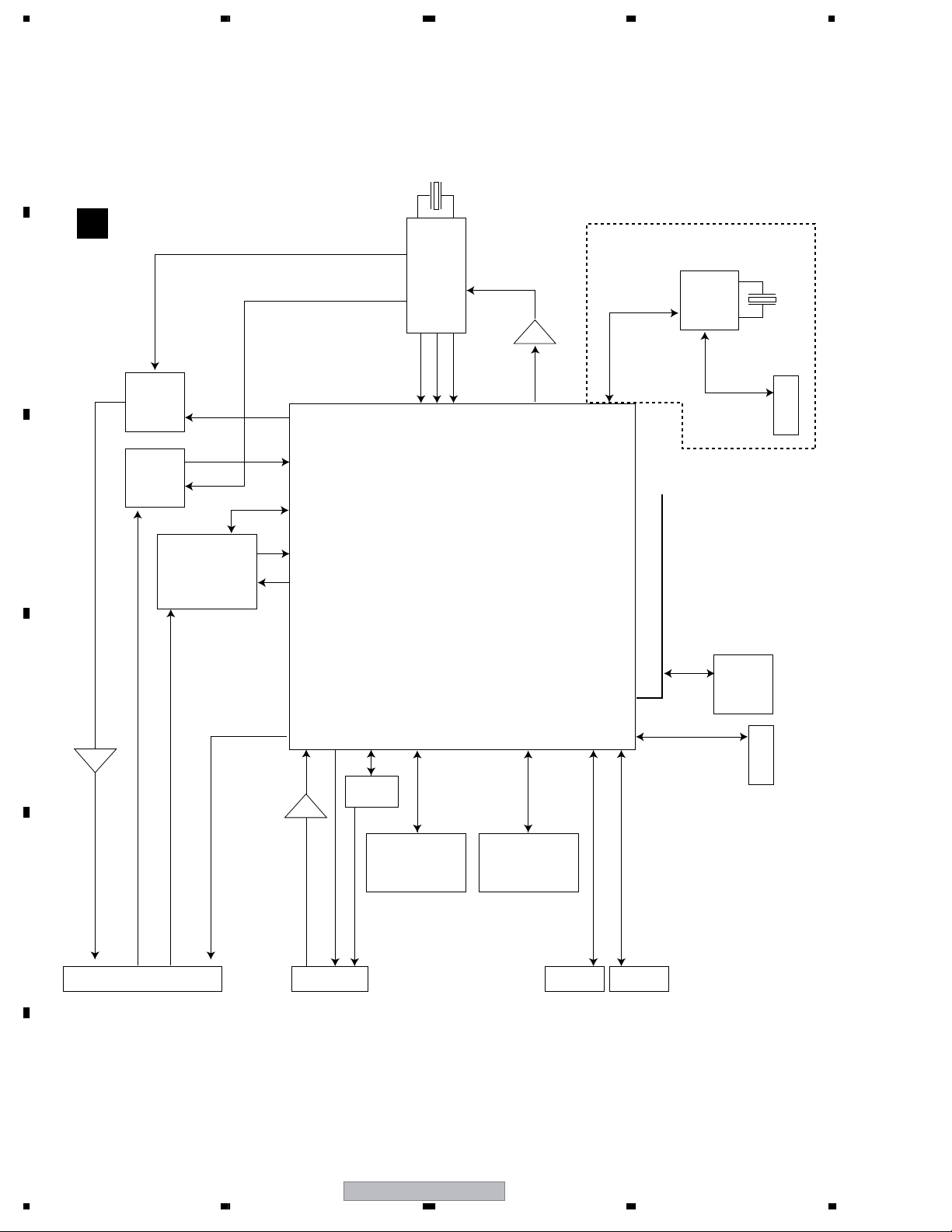
3. BLOCK DIAGRAM AND SCHEMATIC DIAGRAM ..........................................................................................14
3.1 BLOCK DIAGRAM....................................................................................................................................14
3.1.1 OVERALL BLOCK DIAGRAM ............................................................................................................14
3.1.2 MAIN ASSY ........................................................................................................................................16
3.2 OVERALL WIRING DIAGRAM .................................................................................................................18
3.3 TUNB ASSY..............................................................................................................................................20
3.4 JACB(1/2) and FLJB ASSYS....................................................................................................................22
3.5 JACB ASSY(2/2).......................................................................................................................................24
3.6 DVJB ASSY..............................................................................................................................................26
3.7 ATAB ASSY...............................................................................................................................................27
3.8 PSWB and RSWB ASSYS .......................................................................................................................28
3.9 MAIN ASSY(1/5).......................................................................................................................................30
3.10 MAIN ASSY(2/5).....................................................................................................................................32
3.11 MAIN ASSY(3/5).....................................................................................................................................34
3.12 MAIN ASSY(4/5).....................................................................................................................................36
3.13 MAIN ASSY(5/5).....................................................................................................................................38
3.14 POWER SUPPLY UNIT ..........................................................................................................................40
3.15 WAVE FORMS........................................................................................................................................42
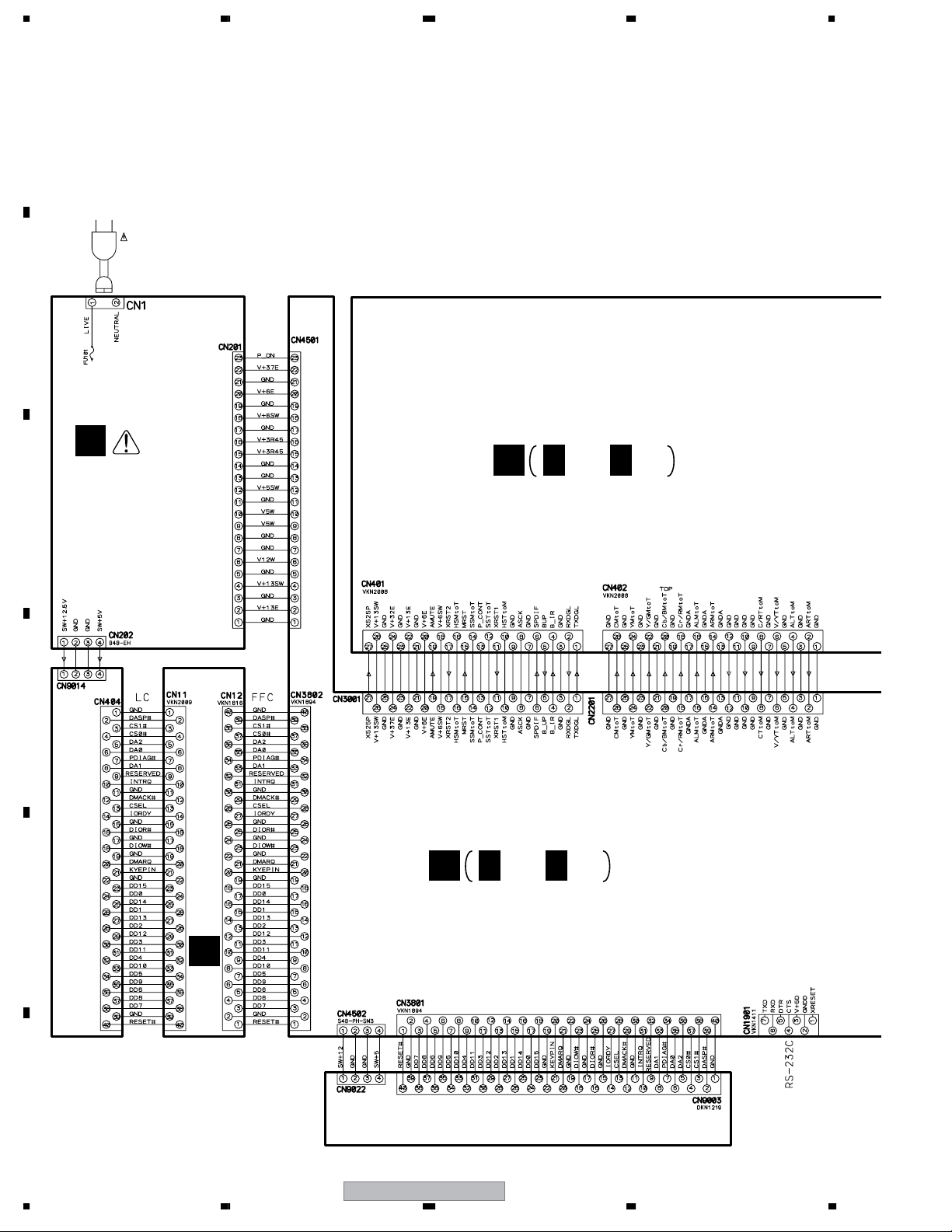
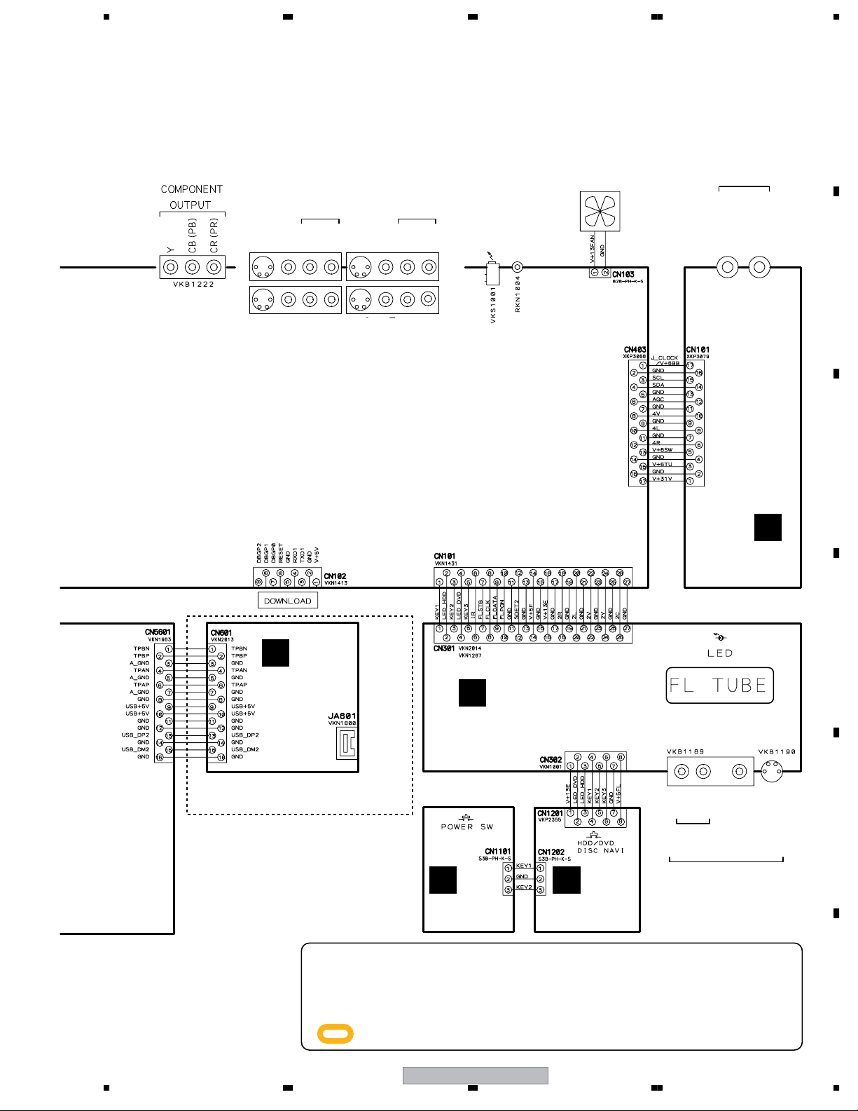
4. PCB CONNECTION DIAGRAM ......................................................................................................................45
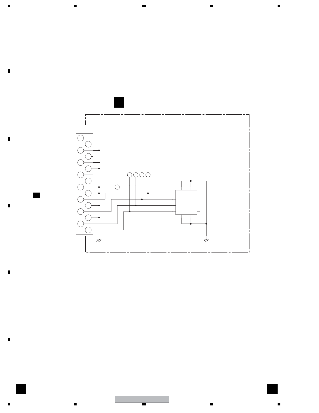
4.1 TUNB ASSY..............................................................................................................................................46
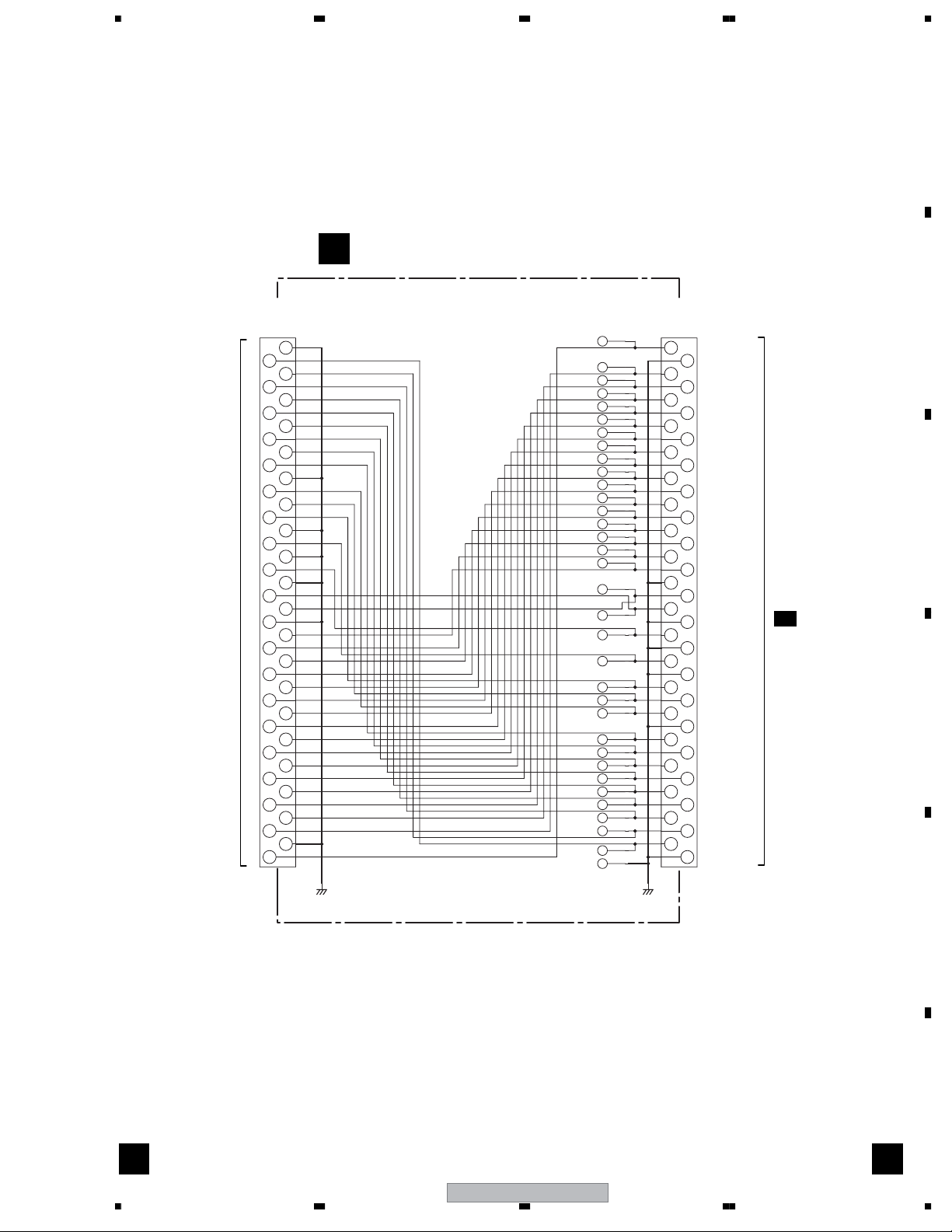
4.2 JACB, FLJB, DVJB and ATAB ASSYS ......................................................................................................48
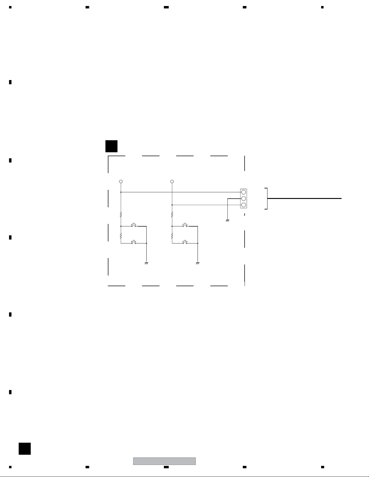
4.3 PSWB and RSWB ASSYS .......................................................................................................................52
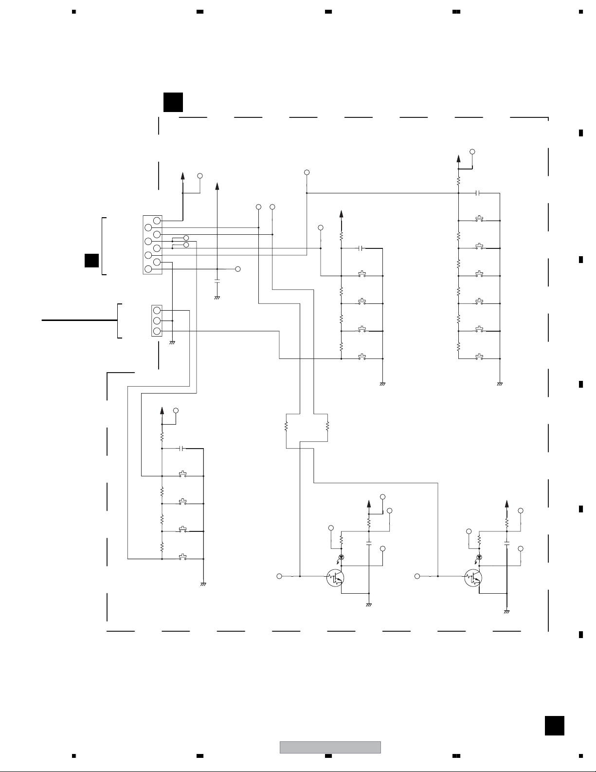
4.4 MAIN ASSY ..............................................................................................................................................54
4.5 POWER SUPPLY UNIT ............................................................................................................................58
5. PCB PARTS LIST............................................................................................................................................60
6. ADJUSTMENT ................................................................................................................................................64
7. GENERAL INFORMATION .............................................................................................................................65
7.1 DIAGNOSIS..............................................................................................................................................65
7.1.1 MODEL SETTING ..............................................................................................................................67
7.1.2 CPRM ID NUMBER AND DATA SETTING .........................................................................................68
7.1.3 FIRMWARE DOWNLOADING METHOD ...........................................................................................72
7.1.4 VIDEO ADJUSTMENT FOR SPECIFIC AREA...................................................................................75
7.1.5 SERVICE MODE ................................................................................................................................79
7.1.6 DV SERVICE MODE...........................................................................................................................93
7.1.7 EPG SERVICE MODE........................................................................................................................96
7.1.8 AGING MODE ....................................................................................................................................99
7.1.9 HDD CHECK MODE.........................................................................................................................101
7.1.10 SETUP SEQUENCE.......................................................................................................................107
7.1.11 DISASSEMBLY ...............................................................................................................................108
7.2 IC ............................................................................................................................................................114
7.3 CAUTIONS ON HANDLING THE HDD...................................................................................................125
7.4 DISC/CONTENT FORMAT.....................................................................................................................127
8. PANEL FACILITIES .......................................................................................................................................129
A
B
C
D
E
56
DVR-533H-S
F
5
7
8
Page 6

1234
1. SPECIFICATIONS
A
B
C
D
E
General
System . . . . . . . . . . . . . . . . . . HDD, DVD-Video, DVD-R/RW,
Power requirements . . . . . . . . . . . . . . . . . . . . . . 120 V, 60 Hz
Power consumption
DVR-531H-S . . . . . . . . . . . . . . . . . . . . . . . . . . . . . . . . .43 W
DVR-532H-S . . . . . . . . . . . . . . . . . . . . . . . . . . . . . . . . .43 W
DVR-533H-S . . . . . . . . . . . . . . . . . . . . . . . . . . . . . . . . .43 W
DVR-633H-S . . . . . . . . . . . . . . . . . . . . . . . . . . . . . . . . .46 W
Power consumption in standby mode 0.42 W
Weight . . . . . . . . . . . . . . . . . . . . . . . . . . . . . 3.9 kg (8 lb 6 oz )
Dimensions . . . . . . . . . . . . . . .420 (W) x 59 (H) x 273 (D) mm
Operating temperature . . . . . . . . . . . . . . . . . +5°C to +35°C
Operating humidity . . . . . . . . . . . . . . . . . . . . . . . . . 5% to 85%
TV format . . . . . . . . . . . . . . . . . . . . . . . . . . . . . . . . . . . . NTSC
Recording
Recording format . . . . . . . . . . . . . . . . . DVD Video Recording
Recordable discs
DVD-RW (DVD Re-recordable disc)
DVD-R (DVD Recordable disc)
Video recording format
Sampling frequency . . . . . . . . . . . . . . . . . . . . . . . . . 13.5MHz
Compression format . . . . . . . . . . . . . . . . . . . . . . . . . . . MPEG
Audio recording format
Sampling frequency . . . . . . . . . . . . . . . . . . . . . . . . . . . . 48kHz
Compression format . . . . . . . . . . Dolby Digital or Linear PCM
Recording time
HDD (160GB)
XP+ . . . . . . . . . . . . . . . . . . . . . . . . . . . . . . . Approx. 23 hours
Fine (XP) . . . . . . . . . . . . . . . . . . . . . . . . . . . Approx. 34 hours
Standard Play (SP) . . . . . . . . . . . . . . . . . . . Approx. 68 hours
Long Play (LP) . . . . . . . . . . . . . . . . . . . . . . Approx. 136 hours
Extended Play (EP) . . . . . . . . . . . . . . . . . . Approx. 204 hours
Super Long Play (SLP) . . . . . . . . . . . . . . . Approx. 272 hours
Super Extended Play (SEP) . . . . . . . . . . . . Approx. 340 hours
Manual Mode (MN). . . . . . . . . . . . . . . . Approx. 23−455 hours
HDD (80GB)
XP+ . . . . . . . . . . . . . . . . . . . . . . . . . . . . . . . Approx. 11 hours
Fine (XP) . . . . . . . . . . . . . . . . . . . . . . . . . . . Approx. 17 hours
Standard Play (SP) . . . . . . . . . . . . . . . . . . . Approx. 34 hours
Long Play (LP) . . . . . . . . . . . . . . . . . . . . . . . Approx. 68 hours
Extended Play (EP) . . . . . . . . . . . . . . . . . . Approx. 102 hours
Super Long Play (SLP) . . . . . . . . . . . . . . . .Approx. 136 hours
Super Extended Play (SEP) . . . . . . . . . . . . Approx. 170 hours
Manual Mode (MN) . . . . . . . . . . . . . . . .Approx. 17−227 hours
DVD-R/DVD-RW
Fine (XP) . . . . . . . . . . . . . . . . . . . . . . . . . . . . . Approx. 1 hour
Standard Play (SP) . . . . . . . . . . . . . . . . . . . . Approx. 2 hours
Long Play (LP). . . . . . . . . . . . . . . . . . . . . . . . Approx. 4 hours
Extended Play (EP) . . . . . . . . . . . . . . . . . . . . Approx. 6 hours
Super Long Play (SLP) . . . . . . . . . . . . . . . . . Approx. 8 hours
Super Extended Play (SEP) . . . . . . . . . . . . Approx. 10 hours
Manual Mode (MN) . . . . . . . . . . . . . . . . . Approx. 1−13 hours
CD-R/RW (WMA, MP3, JPEG, CD-DA)
(Front panel display: off)
(16
9/16 (W) x 2 3/8 (H) x 10 3/4 (D) in.)
Video-CD, CD,
(+41°F to +95°F)
(no condensation)
DVD-VIDEO
(uncompressed)
Tuner
Receivable channels
VHF. . . . . . . . . . . . . . . . . . . . . . . . . . . . . . . . . . . . . . . . 2−13ch
UHF . . . . . . . . . . . . . . . . . . . . . . . . . . . . . . . . . . . . . . 14−69ch
CATV. . . . . . . . . . . . . . . . . . . . . . . . . . . . . . . . . . . C1−C125ch
Timer
Programs . . . . . . . . . . . . . . . . . . . . . . . . 1 month/32 programs
Clock . . . . . . . . . . . . . . . . Quartz lock (12-hour digital display)
Power off memory . . . . . . Approx. 5 years (after manufacture)
Input/Output
VHF/UHF antenna input/output terminal . . . . . . .VHF/UHF set
Video input . . . . . . . . . . . . . . . . . . . . .Input 1,3 (rear), 2 (front)
Input level . . . . . . . . . . . . . . . . . . . . . . . . . . . . . .1 Vp-p (75Ω)
Jacks . . . . . . . . . . . . . . . . . . . . . . . . . . . . . . . . . . . . RCA jack
Video output . . . . . . . . . . . . . . . . . . . . . . . . . . . . . . Output 1,2
Output level . . . . . . . . . . . . . . . . . . . . . . . . . . . . 1 Vp-p (75Ω)
Jacks . . . . . . . . . . . . . . . . . . . . . . . . . . . . . . . . . . . . RCA jack
S-Video input . . . . . . . . . . . . . . . . . . Input 1, 3 (rear), 2 (front)
Y (luminance) - Input level . . . . . . . . . . . . . . . . . 1 Vp-p (75Ω)
C (color) - Input level . . . . . . . . . . . . . . . . . . 300 mVp-p (75Ω)
Jacks . . . . . . . . . . . . . . . . . . . . . . . . . . . . . . . . 4 pin mini DIN
S-Video output . . . . . . . . . . . . . . . . . . . . . . . . . . . . Output 1,2
Y (luminance) - Output level . . . . . . . . . . . . . . . .1 Vp-p (75Ω)
C (color) - Output level . . . . . . . . . . . . . . . . 300 mVp-p (75Ω)
Jacks . . . . . . . . . . . . . . . . . . . . . . . . . . . . . . . . 4 pin mini DIN
Component video output
Output level . . . . . . . . . . . . . . . . . . . . . . . . .Y: 1.0 Vp-p (75Ω)
Jacks . . . . . . . . . . . . . . . . . . . . . . . . . . . . . . . . . . . RCA jacks
Audio input . . . . . . . . . . . . . . . . .Input 1, 3 (rear), 2 (front) L/R
Input level
During audio input . . . . . . . . . . . . . . . . . . . . . . . . . . . . 2V rms
(Input impedance: more than 22 kΩ)
Jacks . . . . . . . . . . . . . . . . . . . . . . . . . . . . . . . . . . . RCA jacks
Audio output . . . . . . . . . . . . . . . . . . . . . . . . . . . Output 1,2 L/R
During audio output . . . . . . . . . . . . . . . . . . . . . . . . . . . 2V rms
(Output impedance: less than 1.5 kΩ)
Jacks . . . . . . . . . . . . . . . . . . . . . . . . . . . . . . . . . . . RCA jacks
Control input . . . . . . . . . . . . . . . . . . . . . . . . . . . . . . . Mini jack
DV input . . . . . . . . . . . . . . . . . . . . . . . . . . . . . . . . .4 pin (front)
(DVR-633/533H-S only) (i.LINK/IEEE 1394 standard)
G-LINK . . . . . . . . . . . . . . . . . . . . . . . . . . . . . . . . . . Mini jack
75Ω (F-shape connector)
, PR: 0.7 Vp-p (75Ω)
P
B
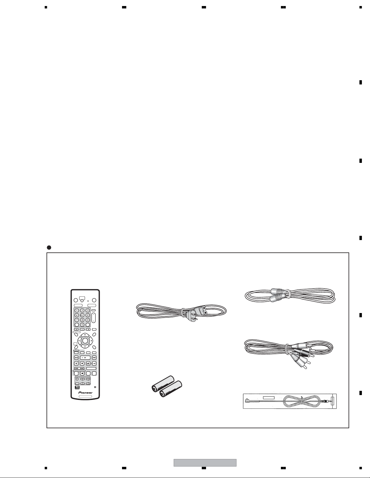
Supplied accessories
Remote control . . . . . . . . . . . . . . . . . . . . . . . . . . . . . . . . . . . . 1
Dry cell batteries (AA/R6P) . . . . . . . . . . . . . . . . . . . . . . . . . . 2
Audio / Video cable (red/white/yellow) . . . . . . . . . . . . . . . . . . 1
G-LINK cable . . . . . . . . . . . . . . . . . . . . . . . . . . . . . . . . . . . .1
RF antenna cable . . . . . . . . . . . . . . . . . . . . . . . . . . . . . . . . . . 1
Power cable . . . . . . . . . . . . . . . . . . . . . . . . . . . . . . . . . . . . . . 1
Blank DVD-RW disc . . . . . . . . . . . . . . . . . . . . . . . . . . . . . . . . 1
Quick Start Guide
Operating Instructions
Warranty card . . . . . . . . . . . . . . . . . . . . . . . . . . . . . . . . . . . . 1
Note: The specifications and design of this product are subject
to change without notice, due to improvement.
F
6
1234
DVR-533H-S
Page 7
5678
A
B
Accessories
• Remote control ×1
(VXX2967)
OPEN/CLOSE
STANDBY/ON
ONE TOUCH
COPY
HDD DVD
ABC
DEF
GHI JKL MNO
PQRS TUV WXYZ
+ CLEAR
CLEAR
AUDIO
SUBTITLE ANGLE
DISC NAVIGATOR
TOP MENU
ENTER
HOME
MENU
TV GUIDE
INFO HELP DISPLAY
REV SCAN
PLAY
PAUSE STOP
CMOK BACK SKIP
CASE
SELECTION
PREV
STEP/SLOW
NEXT
REC
REC MODE TIMER REC
STOP REC
TV CONTROL
INPUT
VOLUME
CHANNEL
SELECT
DVD RECORDER
INPUT
SELECT
CH
PLAY MODE
MENU
RETURN
FWD SCAN
• Power cable ×1
(ADG7075)
• Dry cell batteries ×2
(AA/R6P)
• RF antenna cable(PAL) ×1
(VDE1088)
• Audio / Video cable(1.5m) ×1
(red/white/yellow)
(VDE1077)
• IR Blaster ×1
(VDX1010)
C
D
E
56
DVR-533H-S
F
7
7
8
Page 8
1234
2. EXPLODED VIEWS AND PARTS LIST
NOTES:
Parts marked by "NSP" are generally unavailable because they are not in our Master Spare Parts List.
The mark found on some component parts indicates the importance of the safety factor of the part.
A
Therefore, when replacing, be sure to use parts of identical designation.
Screws adjacent to mark on product are used for disassembly.
For the applying amount of lubricants or glue, follow the instructions in this manual.
(In the case of no amount instructions, apply as you think it appropriate.)
2.1 PACKING
15
14
B
C
KCXV type only
17
16
19
18
13
12
11
10
7
9
8
6
4
2
5
20
3
20
21
1
23
D
25
22
E
F
8
1234
24
DVR-533H-S
Page 9

>
5678
(1) PACKING SECTION PARTS LIST
No. Description Part No.
Mark
1Power Cable ADG7075
2Audio / Video Cable (1.5m) VDE1077
3 RF Antenna Cable VDE1088
4 Remote Control Unit VXX2967
5 Battery Cover AZA7424
No. Description Part No.
Mark
16 Quick Guide (English) VRG1013
17 Quick Guide (French) See Contrast table (2)
18 HDD Caution 8L B VRR1062
19 HDD Caution 8L VRR1063
20 Polyethylene Bag B5 VHL1088
A
NSP 6 Dry Cell Battery (R6P, AA) VEM1030
NSP 7 DVD-RW Disc ver. 1.1 VZZ1003
8 IR Blaster VDX1010
NSP 9 Warranty Card ARY7045
10 Operating Instructions (English) VRB1407
11 Operating Instructions (French) See Contrast table (2)
12 Dual Layer IM (English) VRB1392
13 Dual Layer IM (French) See Contrast table (2)
14 Quick Start Guide (English) VRG1010
15 Quick Start Guide (French) See Contrast table (2)
21 Left Pad VHA1386
22 Right Pad VHA1387
23 Remote Control Holder VHC1139
24 Packing Case See Contrast table (2)
25 Mirror Mat VHL1089
(2) CONTRAST TABLE
DVR-533H-S/KUXV, KCXV, DVR-633H-S/KUXV/CA, DVR-531H-S/KCXV and KUXV/CA are constructed the same
except for the following:
Mark No. Symbol and Description
11 Operating Instructions (French) Not used VRC1306 Not used VRC1306 Not used
13 Dual Layer IM (French) Not used VRC1280 Not used VRC1280 Not used
15 Quick Start Guide (French) Not used VRL1010 Not used VRL1010 Not used
17 Quick Guide (French) Not used VRL1011 Not used VRL1011 Not used
24 Packing Case VHG2597 VHG2598 VHG2599 VHG2654 VHG2596
DVR-533H-S
/KUXV
DVR-533H-S
/KCXV
DVR-633H-S
/KUXV/CA
DVR-531H-S
/KCXV
DVR-531H-S
/KUXV/CA
B
C
D
E
F
56
DVR-533H-S
9
7
8
Page 10
1234
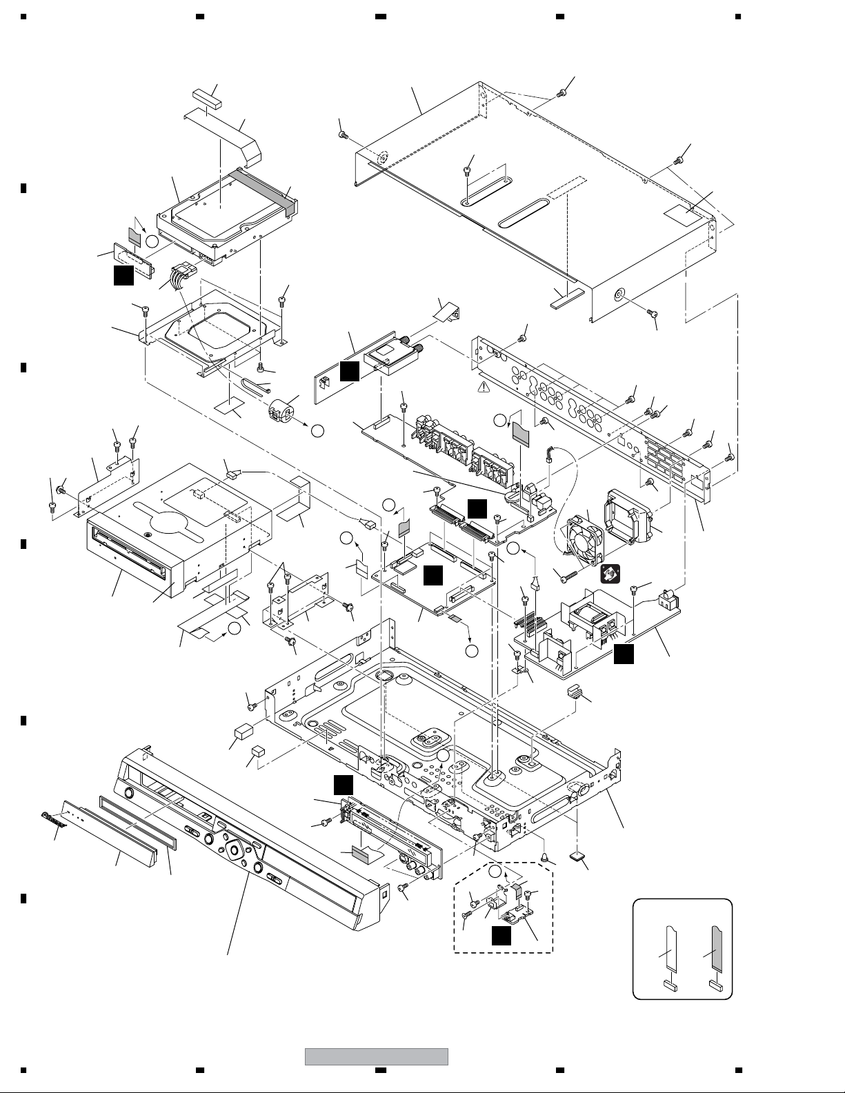
2.2 EXTERIOR SECTION
21
51
55
53
17
18
53
50
48
50
55
36
Cleaning paper
GED-008
49
I
7
53
41
50
50
54
29
24
A
8
E
5
B
C
49
47
D
33
31
49
E
14
49
52
42
26
12
9
15
27
42
49
44
37
42
49
D
42
49
47
16
42
53
C
11
34
1
A
2
Lithium Battery
E
47
49
(CR2032)
D
49
28
49
46
19
48
A
B
49
C
H
6
49
49
49
B
35
49
A
30
45
49
49
B
32
D
10
49
DVR-533H-S,
DVR-633H-S
only
4
22
20
NON-CONTACT
SIDE
CONTACT SIDE
25
23
C
E
38
40
F
39
Refer to
"2.3 FRONT PANEL SECTION".
10
1234
3
49
13
DVR-533H-S
Page 11
>
5678
(1) EXTERIOR SECTION PARTS LIST
No. Description Part No.
Mark
1 TUNB Assy (for service) VXX3024
2JACB Assy See Contrast table (2)
3 FLJB Assy VWG2536
4DVJB Assy See Contrast table (2)
5 ATAB Assy VWV2123
No. Description Part No.
Mark
NSP 31 HDD Stay VNE2369
32 DV Angle See Contrast table (2)
NSP 33 Writer Stay L VNE2371
NSP 34 Writer Stay R VNE2372
NSP 35 PCB Base VNE2378
A
6 MAIN Assy (for service) See Contrast table (2)
7POWER SUPPLY Unit VWR1391
8 HDD See Contrast table (2)
9 DRIVE Assy R9R VXX2987
10 Flexible Cable (16P) See Contrast table (2)
11 Flexible Cable (40P) VDA2065
12 Flexible Cable (40P) VDA2066
13 Flexible Cable (27P) VDA2067
14 Housing Assy (4P) VKP2357
15 Housing Assy (4P) VKP2358
16 Ferrite Core VTH1050
17 DC Fan Motor VXM1120
NSP 18 P. Plate Holder PNY-405
19 Earth Plate TU VBK1156
20 Rubber Foot VEB1349
21 Rubber Spacer (CR) VEB1373
NSP 22 PC Support VEC1749
23 Gasket 10 x 7T VEC2472
24 Gasket 40 x 5T VEC2473
25 Gasket 10 x 25T VEC2475
26 Aluminum Tape 50 x 25 VEF1058
27 Aluminum Tape 135 x 25 VEF1059
28 Bonnet Case S VXX3039
29 Rear Panel See Contrast table (2)
NSP 30 Base Chassis VNB1052
36 Fan Duct VNK5693
NSP 37 Binder (BK-1) ZCA-BK1
38 Pioneer Name Plate VAM1148
39 Tray Sheet VEC2467
40 Tray Panel A VNK5703
41 Bonnet Label VRW2171
NSP 42 Tape ZTA-156A-19
43 • • • • •
44 #6-32 Screw DBA1125
45 Screw See Contrast table (2)
46 Screw BSZ30P060FTC
47 Screw AMZ30P060FTC
48 Screw BSZ30P040FTC
49 Screw BBZ30P060FTC
50 Screw BPZ30P080FTC
51 Screw BPZ30P250FTC
52 Screw BSR30P060FTC
53 Screw BSZ30P060FTC
54 Screw PBZ30P080FTC
55 Screw BBZ30P060FTC
B
C
D
(2) CONTRAST TABLE
DVR-533H-S/KUXV, KCXV, DVR-633H-S/KUXV/CA, DVR-531H-S/KCXV and KUXV/CA are constructed the same
except for the following:
Mark No. Symbol and Description
2JACB Assy VWV2111 VWV2111 VWV2111 VWV2112 VWV2112
4DVJB Assy VWG2523 VWG2523 VWG2523 Not used Not used
6 MAIN Assy (for service) VXX2993 VXX2993 VXX2993 VXX2994 VXX2994
8 HDD 80G WD800BBJKC S VXF1066 VXF1066 Not used VXF1066 VXF1066
8 HDD 160G WD1600BBGUC S Not used Not used VXF1068 Not used Not used
10 Flexible Cable (16P) VDA2064 VDA2064 VDA2064 Not used Not used
29 Rear Panel VNA2771 VNA2771 VNA2792 VNA2794 VNA2794
32 DV Angle VNE2370 VNE2370 VNE2370 Not used Not used
45 Screw VBA1098 VBA1098 VBA1098 Not used Not used
56
DVR-533H-S
/KUXV
DVR-533H-S
/KCXV
DVR-533H-S
DVR-633H-S
/KUXV/CA
7
DVR-531H-S
/KCXV
DVR-531H-S
/KUXV/CA
8
E
F
11
Page 12
1234
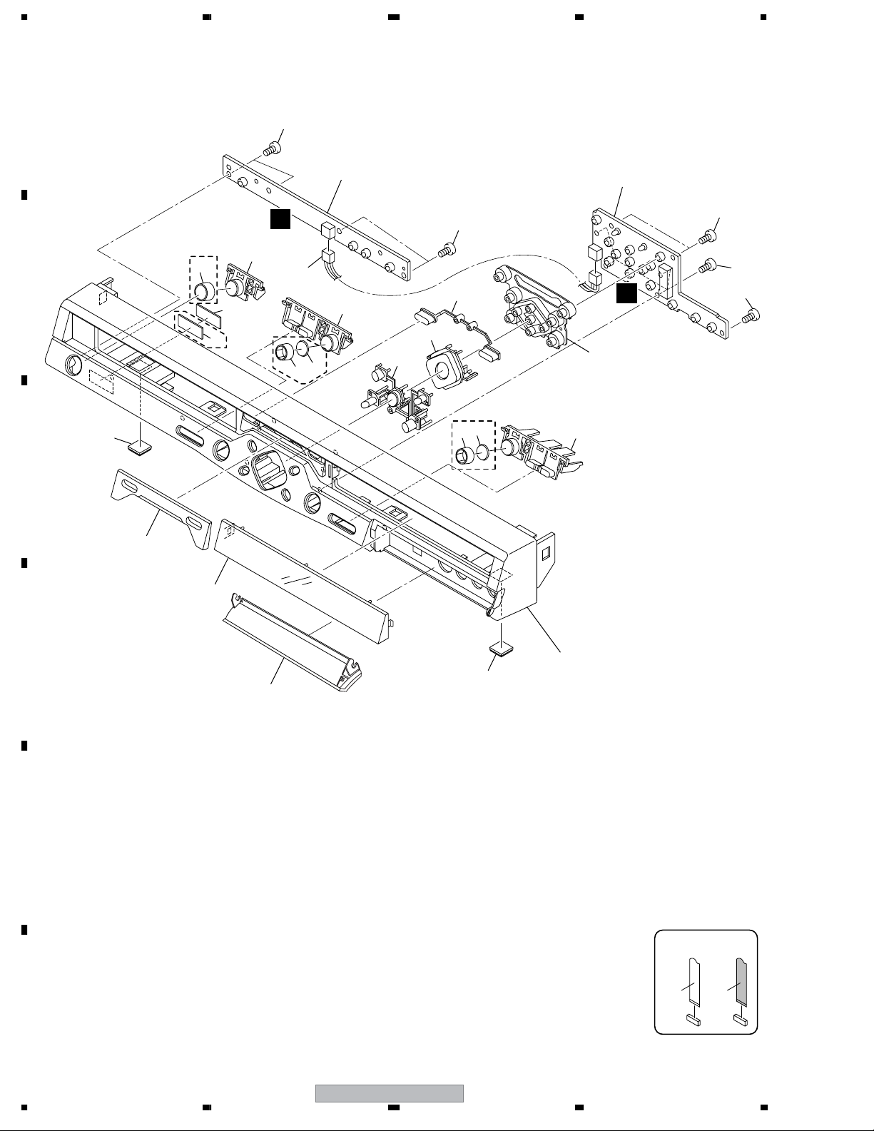
2.3 FRONT PANEL SECTION
A
19
1
F
DVR-633H-S
only
14
B
DVR-531H-S
only
4
C
10
18
11
11
(4/4)
(1/4)
DVR-633H-S
only
15
3
11
(2/4)
16
7
19
8
6
15
DVR-633H-S
only
17
11
5
(3/4)
2
G
19
19
19
9
D
4
12
E
13
F
12
1234
DVR-533H-S
NON-CONTACT
SIDE
CONTACT SIDE
Page 13
5678
(1) FRONT PANEL SECTION PARTS LIST
No. Description Part No.
Mark
1 PSWB Assy VWG2524
2 RSWB Assy VWG2528
3 Housing Assy (3P) VKP2360
4 Rubber Foot VEB1349
5 Rubber Hinge VEB1371
6 Cursor Key VNK5695
7 Enter Key VNK5696
8 Eject Key A VNK5697
9 FL Lens A VNK5698
10 Center Lens AC VNK5699
A
11 Main Key A See Contrast table (2)
12 Door A See Contrast table (2)
13 Front Panel A See Contrast table (2)
14 Key Top A See Contrast table (2)
15 Ring A See Contrast table (2)
16 PLAY Plate A See Contrast table (2)
17 REC Plate A See Contrast table (2)
18 Sensor-matic Seal See Contrast table (2)
19 Screw BPZ30P080FTC
(2) CONTRAST TABLE
DVR-533H-S/KUXV, KCXV, DVR-633H-S/KUXV/CA, DVR-531H-S/KCXV and KUXV/CA are constructed the same
except for the following:
Mark No. Symbol and Description
11 Main Key A VNK5701 VNK5701 Not used VNK5701 VNK5701
11 Main Key Base A Not used Not used VNK5737 Not used Not used
12 Door A VNK5702 VNK5702 VNK5702 VNK5815 VNK5815
13 Front Panel A VNK5730 VNK5730 VNK5818 VNK5817 VNK5817
14 Key Top A Not used Not used VNK5717 Not used Not used
DVR-533H-S
/KUXV
DVR-533H-S
/KCXV
DVR-633H-S
/KUXV/CA
DVR-531H-S
/KCXV
DVR-531H-S
/KUXV/CA
B
C
D
15 Ring A Not used Not used VNK5738 Not used Not used
16 PLAY Plate A Not used Not used VNK5739 Not used Not used
17 REC Plate A Not used Not used VNK5740 Not used Not used
18 Sensor-matic Seal Not used Not used Not used VAN1004 VAN1004
DVR-533H-S
56
7
8
E
F
13
Page 14
1234
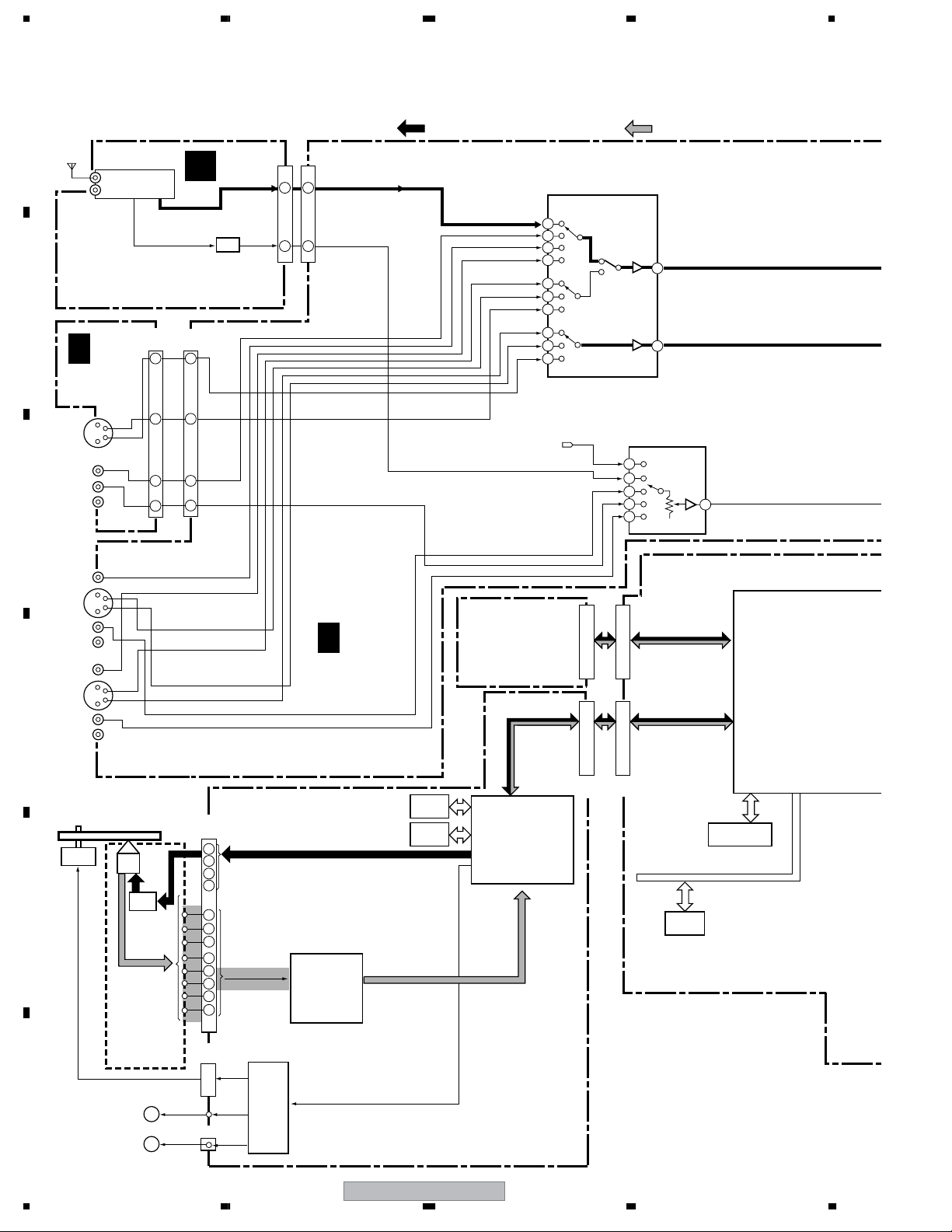
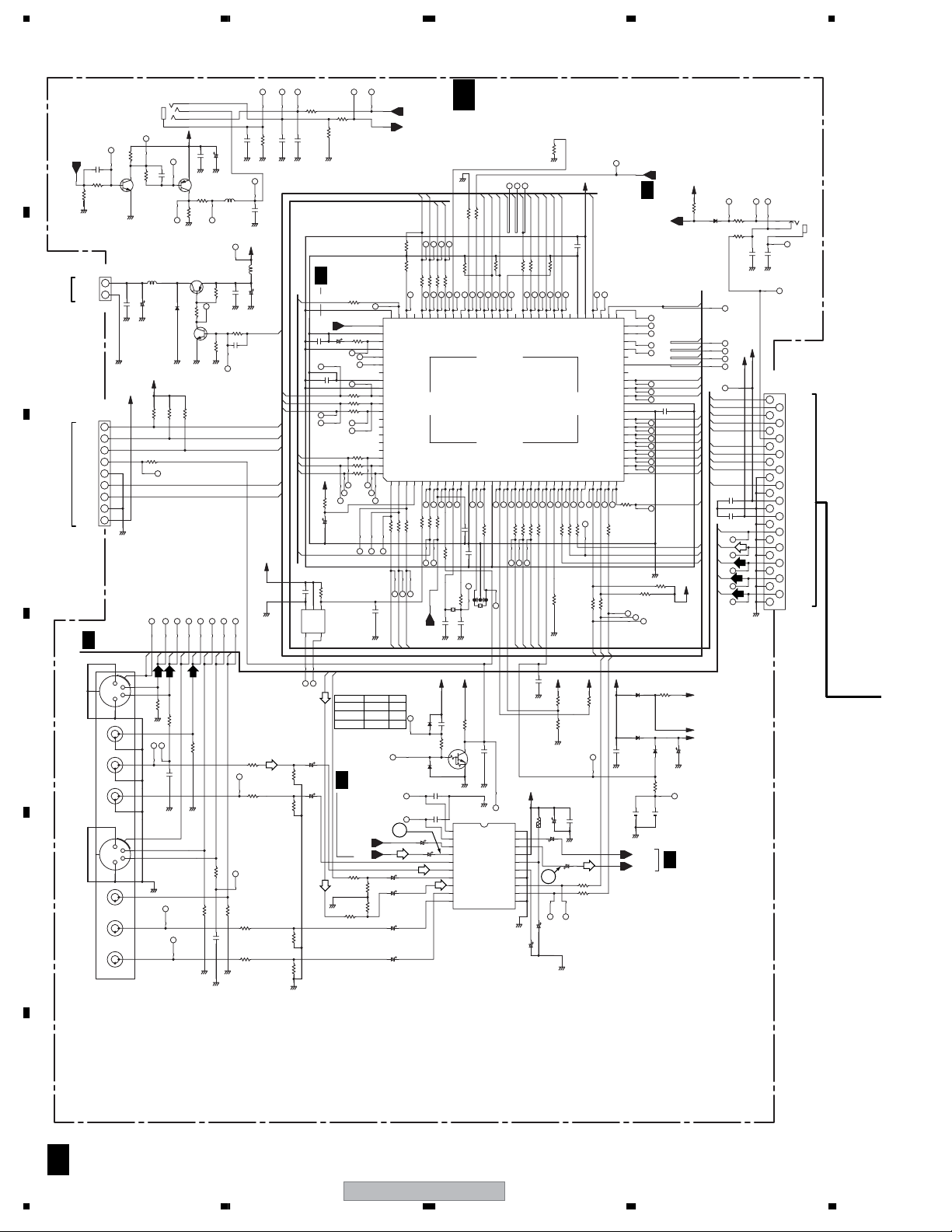
3. BLOCK DIAGRAM AND SCHEMATIC DIAGRAM
3.1 BLOCK DIAGRAM
3.1.1 OVERALL BLOCK DIAGRAM
A
: Recording system signal route
U101 VXF1059
ANT
TV FRONT-END
RF IN
VOUT
AOUT
RF
OUT
17
6
B
CN301(1/2)
(27P)
C
1/2
CIN2
26 26
A
UVL
CN101(1/2)
(27P)
TUNB
ASSY
LPF
CN101
(17P)
10 8
8 10
UVV
UVL
CN403
(17P)
UVV
2V
1V
3V
3Y
1Y
2Y
3C
1C
2C
FLJB
ASSY
JA301
Y/C
VIDEO
C
INPUT2
Y
C
L
R
YIN2
24
24
VIN2
22
22
LIN2
20
20
44
42
40
18
20
22
10
12
1
8
MSL
LIN4
Video Selector
Video Driver
IC401
LA73031V
Audio Selector with Electirc ATT
2
4
6
8
10
: Playback system signal route
V/Y
29
C
31
IC103
BD3823FV
L
18
LIN1
HDD
DSP
IC201
LIN2
LIN3
DVD-VR
DVD-Video
CN202
(40P)
1
8
CN3801
(40P)
CN3802
(40P)
DVD-VR
DVD-Video
[ATA]
[ATAPI]
IC1301
Flash
64Mbit
IC1102
ATA SDRAM
512Mbit
IC1001
R8A34011BG-K
Sysytem Codec
JA103
INPUT1
VIDEO
Y/C
INPUT3
VIDEO
Y/C
D
MOTOR
Y
C
L
R
Y
C
L
R
SPDL
E
Pickup
LD
DRIVE
PICKUP
ASSY
VIN1
VIN3
YIN1
YIN3
CIN1
CIN3
LIN1
LIN3
CN101
A
B
C
D
S4
S3
S2
S1
CN501
(45P)
5
4
3
2
32
36
35
31
38
37
40
39
(12P)
PB DVD/CD
B
1/2
JACB ASSY
RF IC
IC101
UPC3340GC
IC202
IC203
SDRAM
16Mbit
FLASH
16M
UPD63641GM
6CH
F
LOADING
MOTOR
STEPPIONG
MOTOR
M
CN502
M
14
Driver
IC501
BD7997FS
DRIVE ASSY(R9R)
DVR-533H-S
1234
Page 15
5678
• R ch is same as L ch.
I
C101
PMC002A8
Tuner
U-com
Control
Data
CN402(1/2)
(27P)
6
8
L
4
SEL.V/Y
SEL.C
SEL.L
CN2201(1/2)
6
8
4
(27P)
A
Except DVR-531H types
DVJB ASSY
D
DV TERMINAL
TPBN
TPBP
TPAN
4 3 2 1
1 2 4 6
TPBP
TPBN
TPAN
1 2 4 6
IC5101
IEEE1394
Physical IC
TPAP
TPAP
B
C
JA601
CN601
(16P)
CN5601
(16P)
36 37 38 39
UPD72852AGB-8EU
IC1201
DDR
SDRAM
128Mbit
IC1221
DDR
SDRAM
128Mbit
H
MAIN ASSY
C
G
F
FLJB ASSY
2/2
RSWB ASSY
PSWB ASSY
IC3101
PCM1802DB1
10
Audio
11
12
1
A/D
48KHz 20Bit
PLL & VCXO
IC301 PT6315
FL Driver
V301
FL
IC3301
CY244ZXC
IC4201
CM0041BF-K
Video Decoder
IC3201
PCM1742KE
Audio
1-3
D/A Conv.
Key
SW
68
CVBS IN
29
6
7
5
IC3251-1/2
UPC4570G2
CN301(2/2)
(27P)
C IN
CN2201
(2/2)
Cr/R
Cb/B
Y/G
Y
C
7
CN3001
(27P)
18
20
22
24
26
16 16
SPDIF
6 6
(27P)
(27P)
CN402
(2/2)
(27P)
18
20
22
24
26
CN401
Cr OUT
Cb OUT
Y(G) OUT
Y OUT
C OUT
L OUT
Tuner U-com
DVR-533H-S
56
IC501
LA73054
16
14
11
8
6
CN101(2/2)
(27P)
7
B
25
23
21
28
31
33
Cb
Y(G)
Cr
Y
C
V
2/2
JACB ASSY
Y(G)
Cb
Cr
VOUT
YOUT
COUT
LOUT
MSL
MSL : Music Server Lch
JA502
JA503
Y
C
Y
C
JA501
8
Y(G)
Cb
Cr
VIDEO
LINE
OUT 1
L
R
VIDEO
LINE
OUT 2
L
R
OPTICAL
AC-3/PCM
DIGITAL
AUDIO
OUT
D
COMPONENT
VIDEO OUT
E
F
15
Page 16
1234
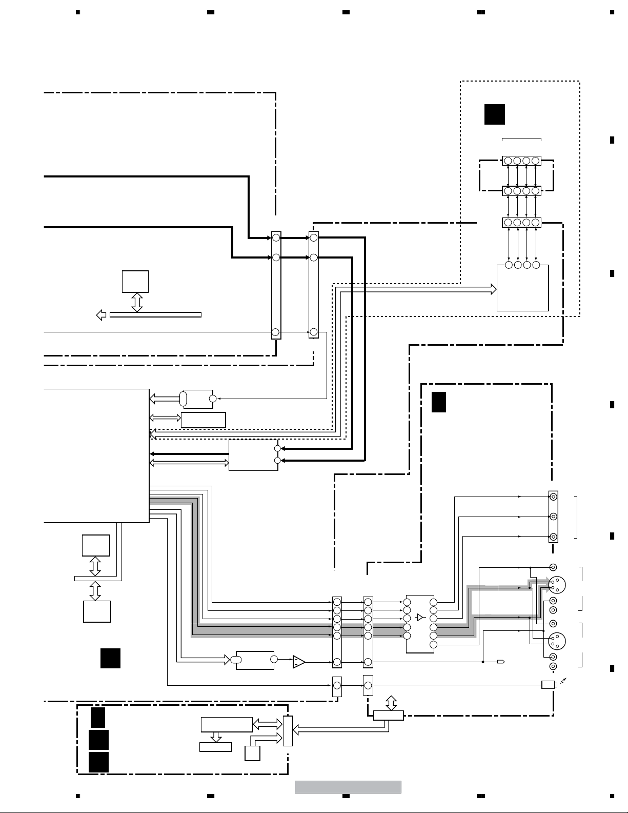
3.1.2 MAIN ASSY
A
MAIN ASSY
H
24M
B
33/36M
IC3201
DAC
IC3101
A/D
C
AUDIO LR IN
D
IC3202
18M
IC4201
Video
Decoder
IC3301
Play Mster clock
and PLL
36M
33M
27M
IC1001
System Codec
IC3303
Except DVR-531H types
HOST BUS
SERIAL
IC5101
Phy
DV_IN
IC1102
FLASH
CN5601
IC3001
VIDEO Y.C.IN
VIDEO Y.C.Yp.Cb.Cr OUT
E
AUDIO LR OUT
CN2201
To JCKB
F
16
1234
Blastor
IR
IC3401
IC1201, 1221
DDR SDRAM
128M x 2
To JCKB
DVR-533H-S
IC1301
DDR SDRAM
512M
To Writer
CN1901CN3801CN3001
To H.D.D
CN1901
Page 17

5678
A
B
C
D
E
56
DVR-533H-S
F
17
7
8
Page 18
1234
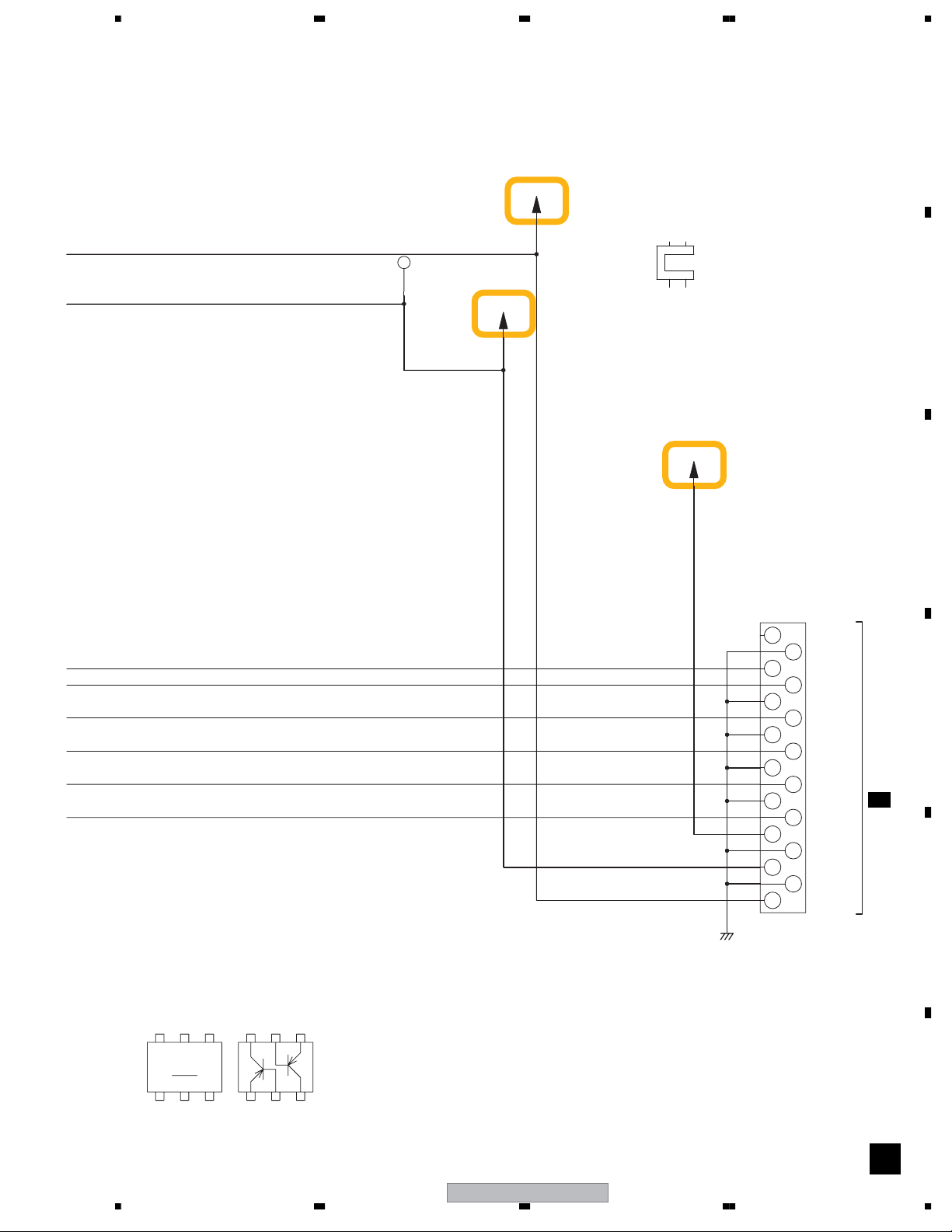
3.2 OVERALL WIRING DIAGRAM
A
AC IN
B
VKN2012
J
POWER SUPPLY
UNIT
C
D
(VWR1391)
VKN2011
H
B
JACB ASSY
H 1/5- H 5/5
B 1/2, B 2/2
(VWV2111:DVR-533H/633H)
(VWV2112:DVR-531H)
VKN2011
E
ATAB ASSY (VWV2123)
(VXX2993:DVR-533H/633H)
(VXX2994:DVR-531H)
E
HDD 80G (VXF1076) 531H/533H
HDD160G (VXF1068) 633H
MAIN ASSY
F
18
1234
DRIVE ASSY R9R (VXX2987)
DVR-533H-S
Page 19
5678
A
S VIDEO
OUTPUT 1OUTPUT 2
OUTPUT X2
VKB1184 - (02)
Video
Left
Audio
Right
Video
S VIDEO
INTPUT X2
VKB1183 - (02)
Left
Audio
Right
INPUT 1INPUT 3
Optical Digital
Audio Output
Control Input
DC FAN MOTOR
(VXM1120)
Antenna
from Antenna
INPUT
to TV
OUTPUT
B
C
TUNB ASSY (VXX3024)
A
D
DVJB ASSY
(VWG2535)
Except
DVR-531H types
÷
When ordering service parts, be sure to refer to "EXPLODED VIEWS and PARTS
LIST" or "PCB PARTS LIST".
÷
The > mark found on some component parts indicates the importance of the safety
factor of the part. Therefore, when replacing, be sure to use parts of identical
designation.
÷
C
FLJB ASSY (VWG2536)
DV INPUT
F
PSWB ASSY
(VWG2524)
: The power supply is shown with the marked box.
G
RSWB ASSY
(VWG2528)
Right
Left
Audio
Video
INPUT 2
(Front)
S VIDEO
D
E
F
56
DVR-533H-S
19
7
8
Page 20
1234
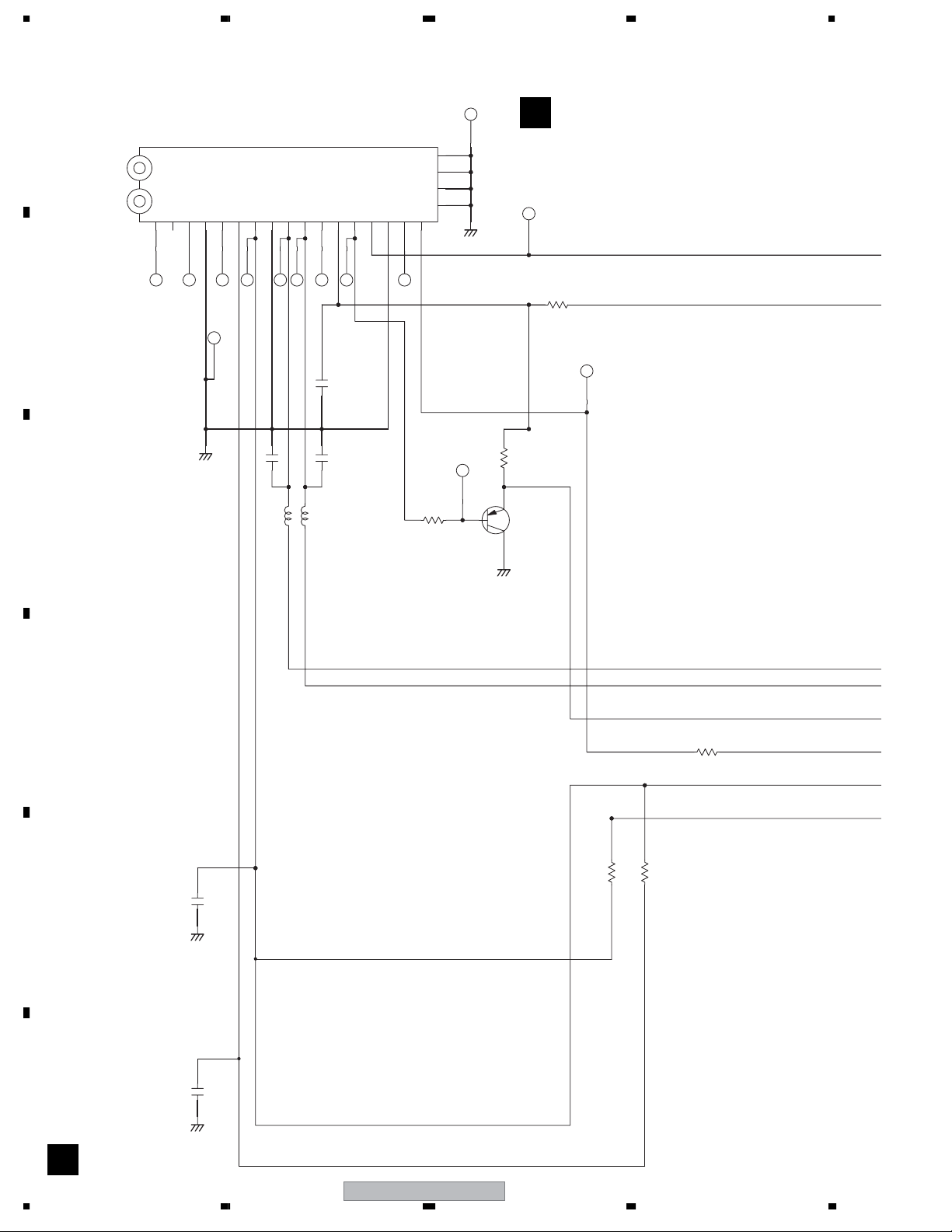
3.3 TUNB ASSY
A
U101
VXF1059
21
20
19
NCNCASNCL OUTNCGND
14325678910 1211 13 14 1715 16
R OUT
SCL
SDA
RF_AGC
MB(5V)
IF_AGC
TU(30V)
GND
AFT
18
UVOUT
GND
B
YB
2200p
C102
CH
GND
C
C106
L102
CH
C107
39p
L103
VTL1081- -T
VTL1081- -T
39p
R104
1k
2SA1576A(QR)-TLB
Q102
R107
E
B
C
GND
TUNB ASSY (VXX3024)
A
<U/V TUNER BLOCK>
R105
0
(2125)
10k
D
R120
0
0
0
R101
YB
R102
E
4700p
GND
YB
F
C123 C122
4700p
GND
20
A
DVR-533H-S
1234
Page 21
5678
A
V+31V
2
1
43
V+5TU
KN101
VNE1948-
B
SCL
SDA
AGC
UVOUT
4L
4R
SW+6V
CN101
XKP3079-
17
16
15
14
13
12
11
10
9
8
7
6
5
4
3
2
1
J_CLOCK
GND
SCL
SDA
GND
AGC
GND
UVOUT
GND
4L
GND
4R
SW+6V
GND
V+5TU
GND
V+31V
C
D
CN403
B 2/2
E
HN1A01FU
CE2B2C
B2 E2
VC
EC2BE
BC2
DVR-533H-S
56
GND
F
A
21
7
8
Page 22
1234
3.4 JACB(1/2) and FLJB ASSYS
JA101
AKN1073-
A
B_IR
GND
/KU,/EU only
toFAN
V+13SW
B
B2B-PH-K-S
To FAN MOTOR
VKN1413- -TBB
DBGP2
DBGP1
DBGP0
RESET
C
D
E
V+5V
DOWNLOAD
INPUT1
INPUT3
2-A1
C164
R186
4.7K
R187
4.7K
CN103
GND
CN102
GND
RXD1
TXD1
GND
B
S
5
V
L
R
S
5
V
L
R
CH100p
1
2
98
1325476
2/2
7
Y
C
14
17
20
1
Y
C
14
17
20
JA103
VKB1183-
G-LINK IN
1K
R184
C
C165
4.7K
R185
B
GND GND
GND
9
10
8
3
4
2
Q112
E
2SC4081(QR)-TLB
GND
LTA102J-T
L102
1m
C103
0.1
C104
100/16
GNDGND
V+5V
V+5V
R177
R180
0
SDET1
11
R209
GND
13
16
19
6
12
15
18
100p CH
R178
100K
(Y)
1C
1Y
75F
R210
C134
GND GND
GND
2
4
3
1
V+5V
C163
GND GND
E
Q107
2SA1576A(QR)-TLB
B
C
R109 L103
150
1K
R110
GND
Q102
2SB1238X(PQ)-T
1
2
D102
4.7K
R103
C
E
1SR154-400-TRB
GND GND
R179
100K
100K
(C)
3Y3C1V
SDET3
75F
75F
R211
0.01 YB
R195
GND GND
C107
0.1
C124
GND GND GND
100/10
VTL1081- -T
V+13SW
EBC
2.2K
0.1
R101
C105
GND GND
Q101
2SC4081(QR)-TLB
R111
B
22K
220p
4.7K
C102
R104
CH
3V
R212
R213
75F
R208
75F
75F
R196
R197
YB
100
C142
0.01
R198
100
GND
C166
GND
L101
C106
100
100
***
FANCTL
DBGP2
DBGP1
DBGP0
RXD1
TXD1
0
R107
CH
100p
10u
470/16
V+5V
GND
R119
CH
CH
100p
100p
C108
C177
GND GND
/KU only
C139
10/50
100K
R190
10/50
100K
R191
100K
100K
R207 R204
GND
0
B
HST_TO_M
TEXTV
2-B2
C109
0.1
C111
0.1
DBGP2
DBGP1
DBGP0
DAT_TO_M
DAM_TO_T
ASCK
HSM_TO_T
0.1
G
IN
NC
4
C148
C149
R112
0
R116
***
2/2
R126
100
C128
2.2/50
R222
R223
R224
V+5V
47K
R165
C167
22/6.3
R113
10K
231
IC102
OUT
BD4846G-TRB
NC
5
2L
2R
Note 1
DVR-533H Not used 0
DVR-633H
DVR-531H
R188
100
GND
R200
100
R131
1K
R141
100
R142
100
R143
100
2/2B
100
100
100
2-D1
2-D1
TXDGL
2-A1
RXDGL
2-A1
R234 R231
7980 7778 727476 75 73 686971 70 64656667 63 59606162 5658 57 55
81
82
83
VDDODA
84
HST_TO_M
85
blank
86
blank
87
blank
88
GND
89
VDD3
90
DBGP2
91
DBGP1
92
DBGP0
93
blank
94
blank
95
blank
96
blank
97
blank
98
99
100
FLDATA
FLSTB
100
100
R153
R154
R152
C125
0.1
FLSTB
FLCLK
FLDATA
GND
R170 R172
Not used 0
39k 6.8k
1SS355-TRB
2
4R
(T)
4L
C157
10/50
C158
100K
R189
10/50
100K
R199
C159
10/50
C160
10/50
B 1/2
GND
100K
LED_DVD
LED_HDD
100
100
R129
R128
TXD1
BLANK
LEDHDD
LEDDVD
81. CVBSIN
82. GND
83. FILTSLC
84. VDDVCO
98. DAT_TO_M
99. DAM_TO_T
100.ASCK
XT1
HSM_TO_T
RESETIRCF2
100
330p
R145
C140
R155
100
R159
VSS1197-
X102
CH
15p
C117
1-A3
GND
GND
V+6E V+5M
YB1u
C130
R214
0
B
Q115
C181
GND GND
0.1
C182
0.1
1
2
L5
3
TunerR
4
TunerL
10/50
5
R1
6
7
R2
8
L2
9
R3
10
L3
100
CSYNC
J_CLOCK
R121
R151
XCHECKER
R123
100K
R233
100K
MRST
AVLIN
blank
SYNCAFT
XCHECKER
IC101
PMC002A8-K
GND
CF1
XT2
MODEL1
VDD1
330
R171
C116
0.1
1
23
560K
CH
X101
10p
C118
CSS1666- -T
10K
R183
C
0.1
C132
E
GND
SELECTR5
ROUT
LOUT
VCC
VRR
FILTERL1
GND
SCL
SDA
GND
IC103
BD3823FV-TBB
RXD1
TXD1
100K
100K
100
100
R225
R127
RXD2
TXD2
RXD1
WDT
ACDET
FLCLK
4312 9786513121110 17161514 211918 20 22 23 24 25 26 27 28 29 30
100
100
100
R114
R144
SELIR
D108
1SS355-TRB
D116
DTC124EUA-TLB
C151
10/50
C152
JACB ASSY (VWV2111: DVR-533H)
(VWV2111: DVR-633H)
(VWV2112: DVR-531H)
100K
R162
FLPON
STATCHG
XP_SAVE
XP_SAVE
J_CLOCK
STATCHG
50. blank
49. blank
48. XAVLTH
47. PSMUTE
33. AMUTE1
32. COMPMUTE
31. MUTEV
KEY1
MODEL2
100
100
R147
R146
KEY1
KEY2
20
19
18
17
16
15
14
13
12
11
GND
C155
SWVION
P_CONT
100
100
R124
R150
FLON
P_CONT
KEY2
KEY3
100
100
R148
R149
AGC
KEY3
C170
GND
V+12VOL
33
R158
C156
100/10
GND
TUON
R235
TUON
SWVION
AGC
BATTDET
R137
GND
V+5V
0.1
GND
C150
(2125)
C153
10/50
1
10/50
I_BG
MUTECTL
100K
I_BG
FUNC
R138
100k
R170
R172
100/16
C154
10/50
GND
V+5M
C110
blank
MUTECTL
SDET2
SDET3
1K1K1K
R139
R140
V+5V
Note 1
Note 1
C138
GND
R193
R192
0.1
GND
AVLOUT
SDET1
R173
0.1
100
100
FANCTL
VDD2
FANCTL
XTHROU
RGBSEL
SWSTBY
SDA
100
R168
R169
SDA
0
5254 53 51
blank
blank
VDD4
YVSEL
SELV3
SELV2
SELV1
SCL
100
R217
100
SCL
XRST1
SDA
SCL
SQU
LET
GND
50
49
48
blank
RFTHRU
47
46
S1
45
44
43
42
41
40
39
38
37
36
35
34
33
32
31
XRST2
XRST1
R216
100
V+6E
1SS355-TRB
D107
D118
1SR154-400-TRB
C178
0.1
GND
ST101
GND
MRST
2-A1
2/2B
SELIR
1-B2
RFTHRU
XAVLTH
PSMUTE
XTHROU
S1
RGBSEL
SQU
LET
C119
0.1
SWSTBY
YVSEL
SELV3
SELV2
SELV1
AMUTE1
COMPMUTE
MUTEV
XRST2
SDET1
SDET2
SDET3
GND
R166
V+5V
R167
4.7K
4.7K
R230
0
C129
D105
1SS352-TRB
GND
1K
R175
+
+
VEM1033-
BT101
Battery(3V)
Lithium Battery
ROUT
2-B1
LOUT
2/2
B
2-B1
V+5V
220K
R156
1SS355-TRB
V+5F
V+5V
V+5M
220/10
D114 R219
R221
V+13E
KEY1
LED_HDD
KEY2
LED_DVD
KEY3
FLSTB
FLCLK
FLDATA
FLPON
SDET2
C168
0.1
C169
0.1
2R
2L
2V
2Y
2C
220
220
CH
C175
680p
GND
V+5F
(Y)
(C)
GND
CONTROL
INPUT
JA102
RKN1004-
2
3
1
0.1
C176
GND
CN101
VKN1431- -TBB
1
KEY1
2
LED_HDD
3
KEY2
4
LED_DVD
5
KEY3
6
IR
7
FLSTB
8
FLCLK
9
FLDATA
10
FLPON
11
GND
12
SDET2
13
GND
14
V+5F
15
GND
16
V+13E
17
GND
18
2R
19
GND
20
2L
21
GND
22
2V
23
GND
24
2Y
25
GND
26
2C
27
GND
F
22
B 1/2
DVR-533H-S
1234
Page 23

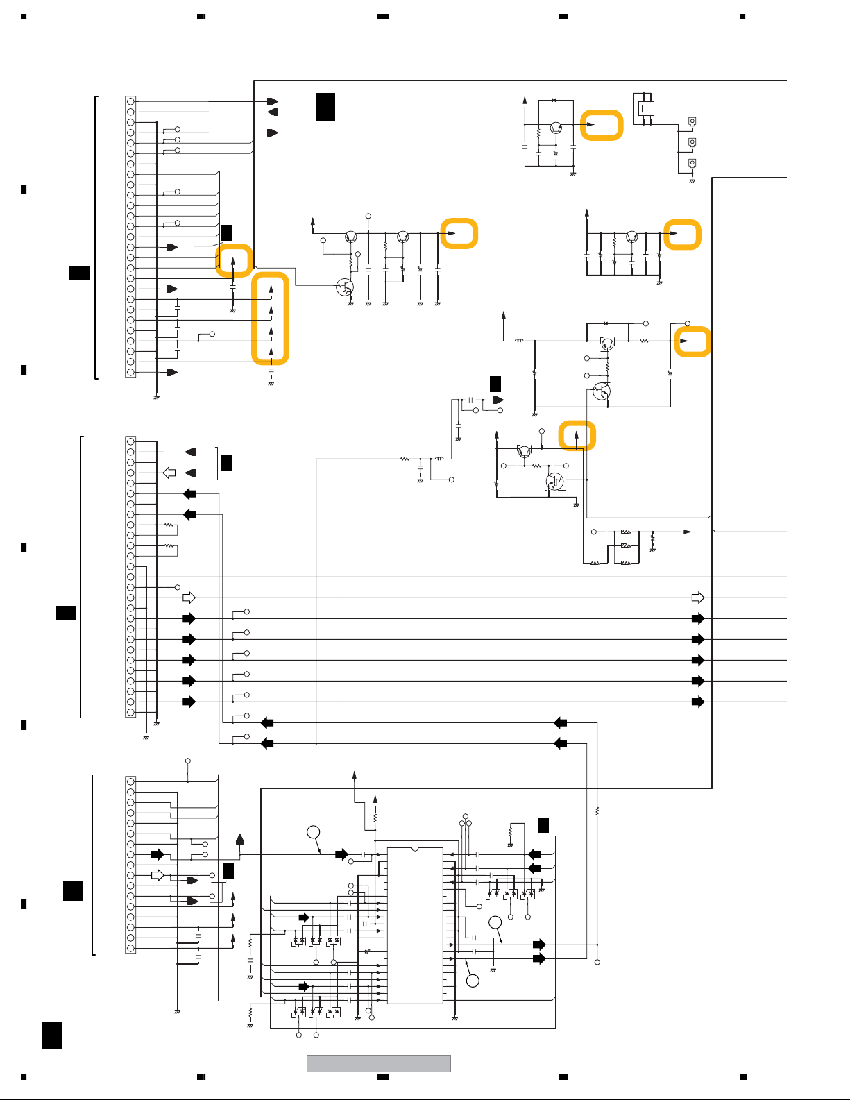
5678
: Video Signal Route
(Y)
FLJB ASSY (VWG2536)
C
: Y Video Signal Route
(C)
: C Video Signal Route
: AUDIO SIGNAL ROUTE (L ch)
(T)
: AUDIO SIGNAL ROUTE (TUNER L ch)
A
CN302
VKM1001-
V+13E
LED_DVD
LED_HDD
KEY1
KEY2
CN1201
KEY3
GND
V+5FL
G
CN301
VKN2014-
(Nichiatsu)
VKN1287-
KEY1
LED_HDD
KEY2
LED_DVD
KEY3
IR
FLSTB
FLCLK
FLDATA
FLPON
GND
SDET2
GND
V+5F
GND
V+13E
GND
2R
GND
2L
GND
2V
GND
2Y
GND
2C
GND
C334
0.1
C323
GND1
1
2
3
4
5
6
7
8
(FCI)
1
2
3
4
5
6
7
8
9
10
11
12
13
14
15
16
17
18
19
20
21
22
23
24
25
26
27
Q307
2SC5712-TLB
C
E
100/16
V+5F_2
V+13E_2
B
R319
LAU220J-TA
V+5FL
0.1
C325
C326
GND1 GND1
GND2GND1
L303
LAU220J-TA
D305
1SS355-TRB
D301
27k
UDZS15(B)-TRB
2SA1576A(QR)-TLB
1
C301
GND1
L301
22
C313
100/10
0.1
GND1
V+13E_2
0.1
C317
GND1 GND1
(Y)
22
R314
270k
Q306
10k
R317
E
B
C
D302
UDZS13(B)-TRB
2
YB
0.01
V+5FL
0.1
C312
VNF1084- -T
1k
C320
R315
0.022
YB
Q308
C
B
E
R320
1.0k
C321
2SC4081(QR)-TLB
V301
VAW1085
11 12 1310917161514 23 2524 26 3027 28 29 31 343332 36 393835 37 40 41 49
S1S5S3S2S4S8S7S6S9
R305
220
R306
220
R307
220
V+5F_2
C316
0.1
V+5FL
GND1
GND1
R304
82k
S10
C304
C308
S11
S13
S12
S14
0.1
4441434042
VSS
LED4
OSC
DOUT
DIN
CLK
9810 576 2341
STB
11
VSS
1215131614
0.1
S15
COM11
COM12
S16
COM8
COM10
COM9
COM1
COM3
COM2
COM5
COM4
COM6
3836373539
VDD
GRID1
GRID3
GRID2
GRID4
GRID5
GRID6
LED1
GRID10
LED2
GRID11
LED3
GRID12
IC301
PT6315
/UPD16315GB-3S
FL DRIVER
KEY1 SEG11
KEY2
SEG10
VDD
SEG1
SEG3
SEG2
SEG4
SEG5
SEG6
S1S3S2S8S7
S5S4S6
COM7
COM7
GRID7
SEG7
COM6
COM8
GRID8
VEE
SEG16
SEG15
SEG14
SEG13
SEG12
SEG8
2120191718
COM5
COM9
34
GRID9
SEG9
22
S9
COM4
23 2524 26 28 2927 30 3231 33
FL
FL-28V
FLDC+
FLDC-
COM3
(Y)
(C)(C)
KN301 KN302
GND1
R316
220
(2125)
VTT1166-
(162-1076-02)
91
82
6
R318
1.2k
YB
0.01
VNF1084- -T
T302
GND2
357
4
D306
RF101L2S-TRB
RF101L2S-TRB
D304
C322
(50V)
C324
C336
0.1
C335
0.1
100/16
10k
R321
10/50
UDZS2R4(B)-TRB
D303
GND1
12321132
D312 D310 D311
D310–312 :
DF3A5.6FU-TLB
COM2
COM1
COM10
COM11
COM12
S16
S15
S14
S13
S12
S11
S10
(Y)
(C)
VNF1130-FL Holder
48
YB
0.01
C303
C333
GND1
GND1
0
R309
FL-28V
0.1
(50V)
GND1 GND2
V+5FL
IC302
AT140BT-16GP(GOODTAKE)
RPM7140-H4(ROHM)
0
R337
(Y)
(C)
C318
GND1
0.1
TS
C319
100/10
JA301
VKB1190-
1
3
4
2
6
1
Vout
2
GND
3
Vcc
S
5
B
C
D
E
9
470p
GND2
R331
0
GND2
8
6
5
3
2
JA302
VKB1189-
3
GND2
R329
0
C331
R327
GND2
0
C332
470p
GND2
VIDEO
7
INPUT2
Lch
/MONO
4
Rch
1
GND2
F
56
DVR-533H-S
B 1/2
C
23
7
8
Page 24
1234
3.5 JACB ASSY(2/2)
CN401
VKN2008-
1
A
B
C
D
E
TXDGL
RXDGL
B_IR
SPDIF
ASCK
HSTtoM
XRST1
SSTtoM
P_CONT
SSMtoT
CN3001
MRST
HSMtoT
XRST2
H 3/5
V+6SW
AMUTE
V+6E
V+13E
V+32E
V+13SW
X525P
ARTtoM
ALTtoM
V/YTtoM
C/RTtoM
GND/GTtoM
CVBS_GR/BTtoM
GNDA
ARMtoT
CN2201
GNDA
ALMtoT
GNDA
H 2/5
Cr/RMtoT
Cb/BMtoT
Y/GMtoT
YMtoT
CMtoT
/V+6BB
CN101
A
V+6SW
V+6TU
V+31V
2
3
GND
4
5
BUP
6
7
GND
8
9
GND
10
11
12
13
14
15
16
17
18
19
20
21
GND
22
23
GND
24
25
GND
26
27
CN402
VKN2008-
1
GND
2
3
GND
4
5
GND
6
7
GND
8
9
GND
10
11
GND
12
13
14
15
16
17
18
19
GND
20
21
GND
22
23
GND
24
25
GND
26
27
GND
CN403
XKP3068-
1
2
GND
3
SCL
4
SDA
5
GND
6
AGC
7
GND
8
4V
9
GND
10
4L
11
GND
12
4R
13
14
GND
15
16
GND
17
GNDA
(T)
(T)
GND
GND
R405
R404
(Cb)
C409
C411 C410
0
0
(Cr)
(Yp)
(Y)
(C)
MRST
1-A3
AMUTE2
1-D3,2-B4
X525P
2-A4
F
GND
B 2/2
24
1234
ASCK
HST_TO_M
XRST1
DAT_TO_M
P_CONT
DAM_TO_T
HSM_TO_T
XRST2
0.1
0.1 0.1
(50V)
ROUT
1-C2
LOUT
1-C2
(Y)
(C)
4L
1-C2
4R
1-C2
C414
C415
SCL
SDA
AGC
0.1
0.1
(50V)
SPDIF
B
V+6SW
C408
GND
V+6SW
V+5TU
V+31V
BUP
1/2
0.1
1/2B
4V
1/2B
GND
GND
SWVION
V+6E
V+13E
V+32E
V+13SW
GND
1-D3
D404-D412
DF3A5.6FU-TLBx9
75F
R435
YB
C462
0.01
75F
R436
TXDGL
1-A2
RXDGL
1-A2
B_IR
1-A1
V+6E
0.1
C412
(C)
(Y)
3C
YVSEL
1C
(C)
2C
12 1212
333
SELV1
3Y
SELV2
(Y)
1Y
SELV3
2Y
12 1212
333
D407 D408
B 2/2
JACB ASSY
(VWV2111: DVR-533H
(VWV2111: DVR-633H)
(VWV2112 : DVR-531H)
2SA1036K(QR)-TLB
Q405
DTC124EUA-TLB
B
V+5VSEL
3
(T)
C442
C443
D405D404 D406
C445
C446
C447
D409
Q403
E
B
R408
C
E
GND
YB0.1
YB0.1
C444
YB0.1
YB0.1
YB0.1
YB0.1
GND
DVR-533H-S
Q404
2SC2411K(QR)-TLB
C
C
E
B
R406
100
1K
0.1
0.1
C417
GND GND GND GND
V+5VI
R420
C438
YB0.1
C450
0.1
C452
470/6.3
C432
C431
R403
470
100/10
100/6.3
C401
180P
GND
/KU, /IBD only
V-DET OUT
V-DET-FIL
V.SYNCOUT
C.SYNCOUT
V-DET-IN
C-OUT
Y-OUT
LPF-CTL
STBY_H
V3-IN
V2-IN
VCC
V1-IN
GND
VCC
GND
VCC
GND
C419
100µ
L405
NC
NC
43
42
41
40
39
38
37
36
35
34
33
32
31
30
29
28
27
26
25
24
23
C418
0
VIDEO SELECTOR
IC401
LA73031V-TBB
144
V4-IN
2
V-DET-CTL
3
NC
4
COMP-H
5
NC
6
NC
7
GAIN-CTL
8
C-IN1
9
YOUT-SEL
10
C-IN2
11
VCC
12
C-IN3
13
GND
14
NC
15
REG
16
NC
17
INSEL1
18
Y-IN1
19
INSEL2
20
Y-IN2NCTEST MODE
21
INSEL3
22
Y-IN3
V+5VI
0.1
C425
1u
C427
470P
GND
<VIDEO SELECTOR BLOCK>
C439
0.1
C440
0.1 0.1YB
C441
0.1 YB
4
GND
V+13SW
C457
V+32E
L401
CTF1399- -T
1/2B
TEXTV
1-A2
V+6E
YB
12 1212
YB
C456
0.1
C453
0.1
GND
GND
Q402
UMF21N-TLB
E
B
UMF21N-TLB
C403
100/10
75F
R437
GND
C455
333
D410 D411 D412
5
(C)
(Y)
SWSTBY
D414
1SS355-TRB
Q412
2SC4081(QR)-TLB
C
B
R432
100
0.1
0.1
C459
C458
C405
10/50
C
R402
560
C2
Q402
E2
B
1/2
2V
1V
3V
GND
E
100/16
GND
V+6TU
B2
C460
GND
(C)
(Y)
0.1
V+6SW
C421
B2
(2125)x 4
V+12VOL
2SC2411K(QR)-TLB
C434
0.1
100/10
D403
1SS355-TRB
Q413
UMF23N-TLB
E
R441
C2
E2
R445
0
0
R423
Q406
C
B
100
R409
C423
C436
100/10
C
B
33K
UMF23N-TLB
Q413
R446
12
R447
12
R448
8.2
0.1
R442
2
413
E
220
C422
0.1
GND
KN401
VNE1948-
C435
100/6.3
GND
C407
C474
1000/6.3
V+5VO
10/50
(Cr)
(Cb)
(Yp)
(Y)
(C)
KN403
KN404
KN405
GND
V+31V
TUON
VNF1084- -T
VNF1084- -T
VNF1084- -T
V+5TU
AMUTE1
Page 25
5678
: Video Signal Route
(T)
: Video Signal Route (TUNER)
(Y)
: Y Video Signal Route
(C)
: C Video Signal Route
(Cr)
: Cr Video Signal Route
(Cb)
: Cb Video Signal Route
(Yp)
: Yp Video Signal Route
: AUDIO SIGNAL ROUTE (L ch)
(T)
: AUDIO SIGNAL ROUTE
(TUNER L ch)
(C)
(Y)
(Yp)
(Cb)
(Cr)
X525P
2-B1
Q503
UMD2N-TLB
B
(C)
Q503
UMD2N-TLB
B2
C
E
7
(Y)
(Yp)
V+5VO
R513
GND
R511
E2
C2
(Cb)
(Cr)
A
V+6SW
SPDIF
LET
SQU
MUTEV
COMPMUTE
100
820
0.1
0.1
0.1
0.1
0.1 YB
C507
C508
C509
C511
C512
C504
C505
YB
1/2B
<VIDEO DRIVER BLOCK>
C515
100/10
YB
YB
R508
YB
R507
0
0
1
0.1
2
0.1
3
4
5
6
7
8
9
10
11
12
13
14
15
16
17
C516
18
100/10
C513
0.1
C514
75W DRIVER with LPF
VCCVCC
CVBS IN 1/2DRIVE1
SQUEEZE
LETTER
MUTE1
C IN
GND ASPECT
Y1 IN
YCMIX
Y2/G SW
Y2(G)IN
MUTE2
LPF SW
Cb(B)IN
GAIN SW2
Cr(R)IN
GND
0.1
IC501
LA73054-TBB
GAIN SW1
VCC
CVBS OUT
GND
C OUT
GND
Y OUT1
GND
GND
Y OUT2
VCC
Cb OUT
GND
Cr OUT
GND
1/2DRIVE2REG
R504 R505
0
C517
C519
1000/6.3
C520
470/6.3
C521
470/6.3
GND
9
V+5VO
0
R506
36
35
C506
34
33
0.1
32
31
30
29
28
27
26
25
C510
24
0.1
23
22
21
20
19
GND
(C)
(Y)
(Y)
(Cb)
(Cr)
C518
1000/6.3
1000/6.3
8
<OUTPUTS>
R501
39
1
D508
C503
2
UDZS5R1(B)-TRB
0
R521
75F
R520
75F
R522
75F
GND
/KU,/IBD,/EU only
JA501
VKS1001-
312
C502
100/10
JA502
VKB1222-
6
1
3
5
4
2
OPTICAL
0.1
Y
Cb/Pb
Cr/Pr
OPTICAL DIGITAL
AUDIO OUTPUTS
B
COMPONENT
V+13E V+5V
D509
D507
1SS355-TRB
1SS355-TRB
1K
680
R570
GND GND GND GND
D506
1SS355-TRB
2.7k
R540
C547
100/16
R556
C548
220/6.3
R562
R530
75F
R529
75F
R523
R525
R526
JA503
VKB1184-
75F
10
75F
75F
(C)
GND
GNDA
GND
7
9
Y
S1
5
C
10
8
13
V1
14
L1
16
17
19
20
1
3
Y
5
C
4
2
12
14
15
17
18
20
OUTPUT 1
R1
S2
V2
OUTPUT 2
L2
R2
(Y)
C523
0.1
R532
75F
R533
100
100
C522
R527
R528
0.1
100
100
AMUTE2_1
B
1-D3
E
Q511
DTA124EUA-TLB
C
11
VCH1241- -T
(47/16)
C549
C550
VCH1241- -T
(47/16)
R557
470
R559
R558
22K
3.9K
R560
470
R561
3.9K
R563
470
R564
3.9K
R565
22K
R566 R534
GNDA
470
R567
3.9K
B
B2
B
B2
C
Q514
HN1C03FU(AB)-T
E
GNDA
C2
Q514
HN1C03FU(AB)-T
E2
GNDA
C
Q515
HN1C03FU(AB)-T
E
GNDA
C2
Q515
HN1C03FU(AB)-T
E2
GNDA
Q510
UMD2N-TLB
AMUTE2
1-D3,2-A1
E2
B2
10K
Q510
UMD2N-TLB
C2
C
B
E
GND GNDA
C
D
E
56
DVR-533H-S
B2C
4E25
6
C232B1E
F
B 2/2
25
7
8
Page 26
1234
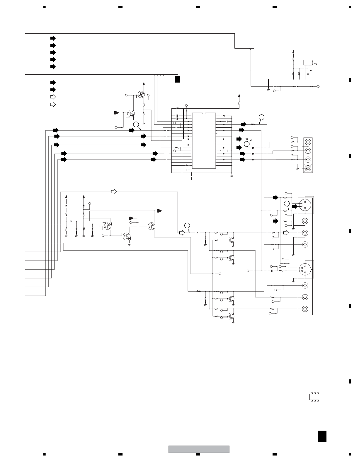
3.6 DVJB ASSY
A
B
CN601
16
GND
USB_DM2
GND
USB_DP2
12
GND
C
CN5601
H 5/5
D
GND
USB+5V
USB+5V
GND
GND
TPAP
GND
TPAN
GND
TPBP
TPBN
10
VKN2013- -TFB
15
14
13
11
9
8
7
6
5
4
3
2
1
GND4
DVJB ASSY (VWG2523)
D
JA601
VKN1800- -TLB
6
TPAP
TPAN
TPBP
TPBN
547
8
DV Input
GND4
1
2
3
E
F
D D
26
1234
DVR-533H-S
Page 27
5678
3.7 ATAB ASSY
ATAB ASSY (VWV2123)(for HDD)
E
A
CN11
VKN2009- -TBB
1
2
3
4
5
6
7
8
9
10
11
12
13
14
15
16
17
18
19
20
21
22
To HDD CN404
23
24
25
26
27
28
29
30
31
32
33
34
35
36
37
38
39
40
CN12
VKN1816-
1
2
3
4
5
6
7
8
9
10
11
12
13
14
15
16
17
18
19
(KEYPIN)
20
21
22
23
24
25
26
27
28
29
30
31
32
33
34
35
36
37
38
39
40
RESET#
GND
DD7
DD8
DD6
DD9
DD5
DD10
DD4
DD11
DD3
DD12
DD2
DD13
DD1
DD14
DD0
DD15
GND
DMARQ
GND
DIOW#
GND
DIOR#
GND
IORDY
CSEL
DMACK#
GND
INTRQ
RESERVED
DA1
PDIAG#
DA0
DA2
CS0#
CS1#
DASP#
GND
B
C
CN3802
H 3/5
D
GND3 GND3
DVR-533H-S
56
E
F
EE
27
7
8
Page 28
1234
3.8 PSWB and RSWB ASSYS
A
B
F
PSWB ASSY (VWG2524)
TP116
C
Switches
S1212:PAUSE
S1213:STOP
S1405:PLAY
S1406:POWER
R1405R1406
5.6k
S1405 S1212
VSG1024- -T VSG1024- -T
S1406 S1213
12k
VSG1024- -T
PLAY
2.85V 2.85V
POWER
3.58V 3.58V
GND2 GND2
TP117
R1212
5.6k
12k
R1213
VSG1024- -T
PAUSE
STOP
GND2
CN1101
S3B-PH-K-S
1
2
3
KEY1_1
GND
KEY2_1
D
E
F
F
28
1234
DVR-533H-S
Page 29
CN302
to FLJB ASSY
C
5678
A
RSWB ASSY (VWG2528)
G
RSWB ASSY
V+13E
LED_DVD
LED_HDD
KEY1
KEY2
KEY3
GND
V+5FL
KEY1_1
KEY2_1
CN1201
VKP2355-
2
4
6
8
CN1202
S3B-PH-K-S
GND
1
3
5
7
1
2
3
VWG2528
VWG2531
V+13E
TP125
GND1
TP122
TP124
V+5FL
GND1
C1204
TP126
TP114 TP115
TP123
YF
0.1
TP128
V+5FL
10k
R1208
VSG1024- -T
R1209
2.2k
VSG1024- -T
R1210
2.2k
VSG1024- -T
R1211
3.3k
VSG1024- -T
C1206
S1208
S1209
S1210
S1211
YF0.1
RECMODE (S Model)
ONE TOUCH COPY
0V
REC STOP
0.90V
REC
1.53V
RETURN
2.18V
(H Model)
V+5FL
10k
R1201
VSG1024- -T
R1202
2.2k
VSG1024- -T
R1203
2.2k
VSG1024- -T
R1204
3.3k
VSG1024- -T
VSG1024- -T
12k 5.6k
R1206 R1205
VSG1024- -T
TP127
C1205
0.1
S1201
S1203
S1206
S1202
S1204
S1205
YF
MENU
0V
RIGHT
0.90V
UP
1.53V
ENTER
2.18V
DOWN
2.85V
HOME MENU
3.58V
B
C
GND1 GND1
V+5FL
TP129
10k
R1401
VSG1024- -T
2.2k
VSG1024- -T
VSG1024- -T
R1404 R1403 R1402
3.3k 2.2k
VSG1024- -T
C1403
0.1
S1401
S1402
S1403
S1404
YF
GND1
DISC NAVI (S Model)
HDD/DVD (H Model)
0V
OPEN/CLOSE
0.90V
TOP MENU
1.53V
LEFT
2.18V
TP113
R1215
0
0
R1217
TP118
R1223
2
BLUE
1
D1207
SLR-343BBT(FGHJ)
C
B
Q1203
DTC124EUA-TLB
1.8k
LED
(HDD)
E
V+13E
C1201 R1225
GND1
0
0.1 YF
Switches
S1201:MENU
S1202:RIGHT
S1203:UP
S1204:ENTER
S1205:DOWN
S1206:HOME MENU
S1208:ONE TOUCH COPY
S1209:REC STOP
S1210:REC
S1211:RETURN
S1401:HDD/DVD
S1402:OPEN/CLOSE
S1403:TOP MENU
S1404:LEFT
DVR-533H-S
56
TP130
TP119
7
TP110
TP112
TP120
R1222
2
AMBER
1
D1203
SLR-343DC(NPQ)-TS
LED
C
B
(DVD)
E
Q1202
DTC124EUA-TLB
D
V+5FL
TP111
0
R1227
180
C1202
TP121
0.1 YF
E
GND1
F
G
29
8
Page 30
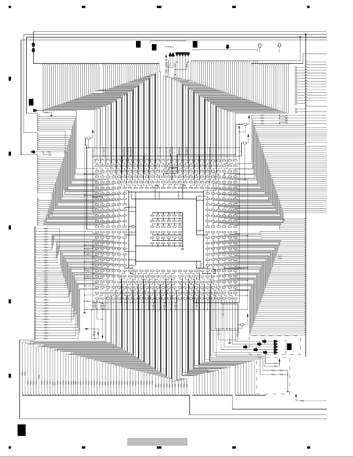
1234
3.9 MAIN ASSY(1/5)
A
(AT)
AT2IORDY
AT2INTRQ
AT2DMARQ
(A1)
(B1)
(C2)
H
4/5
R656CLKI
(C1)
4-B4
B
REC656O6
REC656O7
REC656O4
REC656O2
REC656O1
REC656O0
REC656O5
REC656O3
XRESET
CSYNC
PLLRST
PLLON
TRACE
DVBCK
DVLRCK
DVADATA
DVVCLKO
TRST
DVDAREQ
DVDAACK
DVDADT0
DVDADT1
DVDADT2
DVDADT3
DVDADT4
DVDADT5
DVDADT6
DVDADT7
DVDAADR0
C
DVDAADR1
TSDATB7
TSDATB6
TSDATB5
TSDATB4
TSDATB3
TSDATB2
TSDATB1
TSDATBRDY
TSDATBERR
TSDATBSYN
TSDATBDEN
TSDATB0
TSDATBACK
ARDQS0
ARDATA15
ARDATA14
56*4
ARDATA13
ARDATA12
RAB4CQ560J-T
ARDATA3
ARDATA2
ARDATA1
56*4
ARDATA0
ARDATA7
RAB4CQ560J-T
ARDATA6
ARDATA5
56*4
ARDATA4
ARDATA11
RAB4CQ560J-T
ARDATA10
D
ARDATA9
56*4
ARDATA8
ARDM0
RAB4CQ560J-T
ARDQS1
ARDM1
ARDRS13
ARWE
ARCAS
ARRAS
ARCS0
ARCS1
ARDRS10
ARBA1
ARBA0
82*4
RAB4CQ820J-TRAB4CQ820J-T
ARDRS12
ARDRS11
ARDRS9
82*4
ARDRS8
ARDRS3
RAB4CQ820J-T
ARDRS2
ARDRS1
82*4
ARDRS0
ARDRS7
ARDRS6
ARDRS5
ARDRS4
82*4
ARCLKNO
RAB4CQ820J-T
ARCLKO
E
56(S)
56(S)
7
R1412
R1413
8645328
R1401
(AE3)
(AE4)
(AF4)
(AD3)
DCLKO
DADRS2
DADRS3
DCLKNO
56*4
RAB4CQ560J-T
F
DBI
TDI
TMS
TCK
TDO
(AD4)
DADRS1
R1457
(G5)
(H3)
(H1)
(J6)
(J5)
(J4)
(J3)
(J2)
(J1)
(K5)
(K4)
(K3)
(K2)
(K1)
(L6)
(L5)
(L3)
(M6)
(L2)
(L1)
(M5)
(M4)
(M3)
(M2)
(M1)
(N6)
(N5)
(N4)
(N3)
(N2)
(N1)
(T6)
(P1)
(P2)
(R1)
(R2)
(R4)
R1452
(P5)
(P4)
(P3)
(T4)
(T3)
(R6)
(R5)
(T1)
(U1)
(U2)
(U3)
(U5)
(V1)
(V2)
(V4)
(V5)
(V6)
(W1)
(W3)
(W4)
R1455
R1456
R1458
R1460
R1461
56(S)
R1414
(AF5)
(AD5)
DBA1
DADRS0
RAB4CQ560J-T
R1040
(D3)
(D1)
(E4)
(E3)
(E2)
(E1)
(F5)
(H6)
(F4)
(F3)
(F2)
(F1)
(G4)
(G3)
(G1)
(H5)
1
R1469
75
68
2442
131
628
735
468
7531
735
648
1
2
R1470
R1463
R1459
R1464
R1465
R1466
R1467
R1468
2
1
4
688
5737
64
351
2426
531
886
757
31
42
120(S)
120(S)
(AE5)
(AC5)
(AA6)
R1402
751
613472
DADRS4
DADRS5
DADRS10
56*4
to ATAPI(DVD-RW/R_DRIVE&HDD)
AT2DATA8
AT2DATA9
AT2DATA11
AT2DATA14
AT2DATA7
AT2RESET
AT2DATA1
AT2DATA3
AT2DATA15
AT2DATA5
AT2ADR2
AT2ADR1
AT2DIOW
AT2DATA2
AT2ADR0
AT2CS1
AT2DATA12
(E5)
(D5)
(C5)
(C6)
(A5)
(B5)
(F6)
(E6)
(B6)
L1005
DTL1106- -T
C1053
0.1(S)
C1055
0.1(S)
C1056
0.1(S)
C1057
0.1(S)
GNDD
V+2R5D
56(S)
56(S)
56(S)
56(S)
R1404
35173
R1415
R1418
R1419
R1417
2675682486
(AB8)
(AF7)
(AD8)
(AF8)
(AE8)
(AE7)
(AA9)
DWE
DCAS
DRAS
DDATA0
DDATA1
DDATA2
DADRS12
RAB4CQ560J-T
56*4
(A2)
(B2)
R1035
R1451
R1453
R1454
R1462
(AB6)
DADRS6
(A3)
(B3)
(C3)
10K(S)
GNDD
22(S)
(G2)
56(S)
75(S)
56(S)
75(S)
56(S)
82(S)
82(S)
82(S)
82(S)
82(S)
(Y3)
(Y2)
(W6)
(Y1)
(AA1)
(AA2)
(AB1)
(AB4)
(AA5)
(AA4)
(Y5)
(AC1)
(AC2)
(AD1)
(AD2)
(AC6)
56(S)
56(S)
R1420
R1416
(AF6)
(AD6)
DCS
DBA0
DADRS7
RAB4CQ560J-T
AT2DATA13
(C4)
(A4)
(B4)
(D4)
(AB3)
(AC3)
(AC7)
(AB7)
R1403
135
48
(AA8)
DADRS9
DADRS8
DADRS11
56*4
AT2DMACK
AT2DATA0
AT2CS0
AT2DATA10
AT2DATA6
AT2DATA4
(A6)
(F7)
(E7)
(D7)
(F8)
(E8)
V+1R2
123
1
C1011
B1B3A4B4
C1C2
D1
F1F2G1F4 F3
H1H2H3H4H6 H5
J1
K1K2
L1L2L4 L3L5L6
R1T2R2
T1T4
V1
W1W2
Y1Y2Y3Y4Y5Y6
AA1AA2
AD1
AE1
C1058
0.1(S)
C1008
0.1(S)
C1064
1
C1062
10
C1059
2
YB
R1405
1
42
(AE9)
(AF9)
(AC9)
(AD9)
(AA10)
DDATA6
DDATA4
DDATA5
DDATA3
DDATA7
56*4
RAB4CQ560J-T
AT1ADR2
AT1CS1
AT2DIOR
AT1DIOR
AT1DMACK
AT1ADR1
(C7)
(A7)
(D8)
(C8)
(B8)
(A8)
1
C1007
A2B2A1
A3A6B5A5
D2D4C3D3
E2 E1E3E4E6 E5
G2
G3G4
J2J4K3J3K4J5J6
M2N1M1
N2N4
N3N5
P2 P1P4 P3P6 P5
T3
U2 U1U4 U3U6 U5
V2V4
V3V5V6
W3W4
AB2 AB1
AC2 AC1AC3AC4AC6AC7 AC5
AD2
AD3AD4
AE2
AF2 AF1AF3AF4AF6AF7 AF5
C1050
0.1(S)
0.1(S)
C1063
0.1(S)
220/4
(AF1)
(AF2)
VREF
56(S)
56(S)
91(S)
91(S)
R1406
7358573641
R1425
R1426
R1421
R1422
(AC10)
(AD10)
(AB10)
(AF10)
(AA11)
DDM0
DDM1
DDQS0
DDQS1
DDATA8
RAB4CQ560J-T
56*4
AT1CS0
AT1DATA0
AT1ADR0
AT1DATA1
(F9)
(E9)
(D9)
(C9)
C4C5D5C6
F5F6
K5K6
M4 M3
M5M6
R4 R3
T5
W5W6
AA4 AA3AA6 AA5
AB4 AB3
AB5
AD5AD6
AE4 AE3
AE5AE7 AE6
64
218
(AC11)
(AB11)
(AE11)
DDATA9
DDATA10
DDATA11
56*4
RAB4CQ560J-T
AT1DATA2
AT1DATA3
(A9)
(B9)
R1407
(AF11)
DDATA12
AT1RESET
AT1DIOW
(F10)
(E10)
0.1(S)
C1009
B6
D6
G6 G5
N6
R6T6R5
C1018
C1019
0.1(S)
1000p(S)
AB6
(AB12)
(AA12)
DDATA13
DDATA14
RAB4CQ560J-T
AT1DATA8
AT1DATA5
AT1DATA4
AT1DATA6
(A10)
(F11)
(B10)
(C10)
0.1(S)
C1010
A8A9 A7
B7B8B9
C7C8C9
D8D9 D7
E7E8E9
0.1(S)
C1032
C1015
0.1(S)
C1016
0.1(S)
VCORE
YB
C1017
0.01(S)
1
C1020
C1021
0.01(S)
AA7
AB7
AD7
R1408
28
(AD12)
(AF12)
(AE12)
DDATA15
DDATA16
DDATA17
56*4
3/5
H
AT1DATA9
AT1DATA7
(E11)
(D11)
F9 F8 F7
1
C1031
C1004
10
AE8AE9
164735473621285
(AC13)
(AA13)
DDATA19
DDATA18
RAB4CQ560J-T
AT1DATA12
AT1DATA10
AT1DATA11
(C11)
(A11)
(B11)
F10F11F13 F12
AA9 AA8
AB10AB11
AB9 AB8
AC9 AC8
AC10AC11AC13 AC12
AD9 AD8
AE10AE11
AF9 AF8
R1409
(AE13)
(AD13)
DDATA21
DDATA20
56*4
AT1DATA13
AT1DATA14
AT1DATA15
AT1INTRQ
(C12)
(E12)
(D12)
(B12)
A11 A10A13 A12
B11 B10
C11 C10
D11 D10
E11 E10E12E13
C1033
L11L13 L12
M11M12M13
N11
P11P13 P12
R11R13
T11
System Codec
AA11 AA10
AD11 AD10
AF11 AF10AF13 AF12
1
C1006
56(S)
R1427
(AA14)
(AF13)
(AB14)
DDATA23
DDATA22
4/5H
V+3D
AT1IORDY
AT1DMARQ
(A12)
(B13)
R1034 R1033
22(S) 1K(S)
(C13)
(A13)
B12B13
C12C13
D13 D12
C1030
0.1(S)
0.1(S)
N13 N12
R12
T13 T12
IC1001
R8A34011BG-K
AA12
AA13
AB13
AB12
AD12AD13
AE12AE13
C1051
1000p(S)
91(S)
56(S)
91(S)
R1428
R1424
R1423
(AC14)
(AD14)
(AF14)
DDM3
DDM2
DDQS3
DDQS2
RAB4CQ560J-T
56*4
3-C3
3-D2
AMCLK1
DVAMCLKI
AMCLK2
VMCLK
H
3-C2,4-A1
DVVCLKI
4-C2
SDA
SDCL
4-C2
VDPIDO20
R1036
1K(S)
R1039
R1038
10K(S)
10K(S)
(A15)
R1037
22(S)
GNDD
C1012
1000p(S)
A15 A14A17 A16
B14B15
C15
C14
D15 D14
E15 E14E17 E16E20 E18E19
F14F15F17 F16F18F20 F19
(B15)
(F14)
(E14)
(A14)
(F13)
(F15)
1
C1001
C1003
1000p(S)
B17 B16
B18B19
C17 C16
C18C20
D16
D17
C1027
C1026
0.1(S)
C1029
C1028
0.1(S)
0.1(S)
L15 L14L16
M15 M14
M16
N15 N14N16
C1025
P15 P14P16
1000p(S)
R14R15
R16
T15 T14T16
GNDD
AA15 AA14AA17
AA16
AA18
AB15 AB14
AB16
AB17
AC15 AC14AC16AC17AC18AC20 AC19
AD14
AD15
AD16AD17
AE17 AE16
0.1(S)
75173315
(AF16)
(AE16)
(AD16)
(AF15)
DDATA27
DDATA30
DDATA28
DDATA29
56*4
RAB4CQ560J-T
AD18AD19
AE18AE20
R1411
(AC16)
DDATA31
AE14AE15
AF14AF15AF17 AF16AF19 AF18AF20
C1005
R1410
82644862
(AE15)
(AC15)
(AB15)
(AA15)
DDATA25
DDATA24
DDATA26
3/5,4/5
VDPIDO22
VDPIDO28
VDPIDO24
VDPIDO26
VDPIDO10
(D16)
(A16)
(B16)
(C16)
(E16)
A20
A19 A18
B20
C19
D20 D19 D18
1
C1024
0.1(S)
0.1(S)
C1023
1000p(S)
C1022
AA20 AA19
AB20 AB19 AB18
AD20
AE19
C1052
0.01(S)
(AB16)
(AE17)
(AF17)
PHYSCLK
DVREQ
PHYCTL1
PHYCTL0
VDPIDO27
VDPIDO12
VDPIDO23
VDPIDO25
VDPIDO21
VDPIDO11
VDPIDO13
VDPIDO29
(D17)
(A17)
(B17)
(C17)
(F16)
(A18)
(E17)
A21A22
B21B22
C21
C22
D22 D21
E22 E21E24 E23E26 E25
F21F22
G21G22
H22 H21H24 H23H26 H25
J21J22
K21K22
L21L22L24 L23L26 L25
M22
M21M23
N21N22
P22 P21P24 P23P26 P25
R21
R22R23
T22
T21
U22 U21U23U24U26 U25
V21V22
W21
W22
Y22 Y21Y24 Y23Y25Y26
AA21AA22
AB21AB22AB24 AB23
AC22 AC21AC24 AC23AC26 AC25
AD22 AD21
AE22 AE21
AF22 AF21AF24 AF23AF26 AF25
C1034
C1035
(AF18)
(AC17)
(AD17)
(AA16)
(AA17)
(AB17)
LPS
PHYLREC
PHY_DATA1
PHY_DATA6
PHY_DATA0
VDPIDO18
VDPIDO16
VDPIDO14
(D18)
(B18)
(C18)
A23A24
B23B24
C23
C24C26
D24
D23
F23F24
G23G24
J24 J23
K23K24
M24
N24 N23
R24
T23
T24
V24 V23
W24 W23
AA23AA24
AD24 AD23
AE23AE24
0.01(S)
0.01(S)
GNDD
(AE18)
(AD18)
PHY_DATA2
PHY_DATA7
(VD)
VDPIDO17
VDPIDO15
VDPIDO19
(A19)
(B19)
(F18)
(E18)
C25
D25D26
G25G26
R25R26
T25T26
W25W26
AB25AB26
AD25AD26
(AE19)
(AA18)
PHY_DATA5
PHY_DATA3
PHY_DATA4
VDPIDI2
VDVSYNCI
VDPIDI0
(C19)
(E19)
(F19)
C1002
C1013
A26 A25
B26 B25
F26 F25
J26 J25
K26 K25
M26 M25
N26 N25
V26 V25
AA26 AA25
AE26 AE25
Video DAC
Power
YB
(Cb)
(AD19)
(AB18)
REC656I6
VDPIDI1
VDPIDI3
VDPIDI4
(A20)
(B20)
(C20)
V+3D
L1008
DTL1106- -T
2
220/4
V+3D
L1004
13
2
1
C1040
1000p(S)
V+3V
L1007
1
3
2
10
C1036
(AA19)
(AC19)
REC656I0
REC656I7
REC656I5
VDPIDI5
VDPIDI8
(D20)
(E20)
31
DTL1106- -T
(AE20)
(AF20)
REC656I3
VDHSYNCI
VDPIDI6
LRCKO
(C21)
(F20)
(A21)
(B26)
(C25)
(C26)
(E23)
DTL1106- -T
(Yp)
(C)
(AD21)
(AE21)
REC656I1
REC656I4
REC656I2
VDPIDI9
VDPIDI7
(D21)
(E21)
(Cr)
(Y)
ADATAO
SRCBCLKI
SRCLRCKI
ACMOD0
(A22)
(B22)
(C22)
R1011
R1012
R1013
R1014
(XCHK)
USB&LAN_XRST
Video DAC Power
REXT1
(AB21)
REXT2
(AC20)
SRCBCLKO
BCKI
ACMOD1
(D22)
(A23)
(B23)
(E22)
22(S)
22(S)
22(S)
22(S)
SRCMODE0
TUSCLK
XVQERST
SRCMODE1
TUACK
ADC_RST
EDINT
LANINT
TUREQ
DVCINT
XGRRST
DVINT
SRCRST
XBRST
AUDIO_MUTE
X525P
232TX
RFF
XYCbCr
DDRCKE
BuCOMTX
TURX
UARTTX
BuCOMRX
232RX
UARTRX
TUTX
Analog Video OUT
(AF26)
(AE25)
(AF24)
(AE23)
(AF22)
(AC21)
CBU2
CBU1
(AC22)
R1501
3.9KF
R1503
3.9KF
SRCDATAO
LRCKI
(A24)
(C23)
R1031
R1032
USBINT1
DVCSEL
ROUT
GOUT
BOUT
COUT
YOUT
YB
YB
ADATAI
(B24)
111
2-B4
2-B4
2-B4
2-A4
2-A4
V+3V
C1513
C1514
R1502
68(J)
R1504
GNDD
0.1(S)
0.1(S)
0
SRCLRCLKO
BCKO
SRCDATAI
(C24)
(A25)
(B25)
(D25)
(D26)
(E24)
(E26)
(F22)
(F23)
(F24)
(F25)
(F26)
(G21)
(G22)
(G23)
(G24)
(G25)
(G26)
(H22)
(H23)
(H24)
(H25)
(H26)
(J21)
(J22)
(J23)
(J24)
(J25)
(J26)
(K21)
(K22)
(K24)
(K25)
(K26)
(L21)
(L22)
(L23)
(L24)
(L25)
(L26)
(M21)
(M22)
(M23)
(M24)
(N21)
(N22)
(M25)
(M26)
(N23)
(N24)
(N25)
(N26)
(P26)
(P24)
(P22)
(R26)
(R25)
(R24)
(R23)
(R22)
(R21)
(T26)
(T25)
(T24)
22(S)
22(S)
(T21)
(U26)
(U25)
(U24)
(U23)
(U22)
(U21)
(V26)
(V25)
(V24)
(V23)
(V22)
(V21)
(W26)
(W25)
(W24)
(W23)
(W22)
(W21)
(Y26)
(Y25)
(Y23)
(Y22)
(AA26)
(AA25)
(AA24)
(AA23)
(AB26)
(AB25)
(AB24)
(AB23)
(AC26)
(AC25)
(AC24)
(AC23)
(AD26)
(AD24)
SPDIFI
SPDIFO
(A26)
H
TX2
RX2
HCS0
HCS1
HCS4
HCS5
INT5
TX1
INT7
ACMOD0
ACMOD1
SPICS
TRACE
HDREQ0
HADRS3
HADRS0
HADRS4
HADRS2
HADRS5
HADRS6
HADRS7
HDREQ1
HADRS1
HADRS8
HADRS9
HADRS11
HADRS12
HADRS10
HADRS14
HADRS16
HADRS17
HADRS18
HADRS13
HADRS19
HADRS20
HADRS22
HADRS23
HDATA0
HADRS15
HADRS21
HDATA1
HDATA2
HDATA3
HDATA5
HDATA4
HDATA6
HDATA7
HDATA8
HDATA9
HDATA10
HDATA11
HDATA12
HDATA14
HDATA13
HDATA15
HDACK0
HDACK1
NSDATX0
NSDARX0
NSDARX1
HWAIT
NSDATX1
NSCS0
NSCS1
NSCLK0
NSCLK1
SPICS
SPIDATAI
SCLK0
SCLK1
SPIDATAO
SPICLK
TESTMOD1
TESTMOD2
TESTMOD0
TESTMOD3
TESTMOD4
TESTMOD5
2/5
V+3D
R1064
RTS0
CTS0
RTS2
HDOE
HCS0
HCS1
HCS3
HCS2
HWS1
HCS4
HCS5
HWS0
INT1
CTS0
INT0
INT2
INT3
INT4
RTS2
INT5
INT6
INT7
INT8
CTS1
CTS2
CTS3
RTS0
RTS1
RTS3
10K(S)
TX2
TX1
RX0
TX3
RX1
RX2
RX3
TX0
111111111111
11
11
H 1/5
30
DVR-533H-S
1234
Page 31

5678
DVREQ
(T23)
(T22)
CODEC
ATA
(AT)
V+3D
R1043
10K*4
375
468
RAB4CQ103J-T
2
71
R1045
5
68
10K*4
3
4
RAB4CQ103J-T
1
2
7
8
R1047
64
10K*4
35
RAB4CQ103J-T
1
2
R1090
10K(S)
R1091
10K(S)
R1092
10K(S)
R1093
10K(S)
R1068
10K(S)
R1067
10K(S)
735
864
R1051
10K*4
RAB4CQ103J-T
1
2
R1052
10K(S)
R1074
***(S)
R1075
10K(S)
R1053
10K(S)
R1055
10K(S)
R1054
648
10K*4
357
RAB4CQ103J-T
1
2
R1070
10K(S)
R1071
10K(S)
R1078
10K(S)
R1079
10K(S)
R1080
***(S)
R1081
10K(S)
R1058
10K(S)
R1059
10K(S)
R1060
10K(S)
R1061
10K(S)
R1062
10K(S)
R1063
10K(S)
R1082
10K(S)
R1083
10K(S)
GNDD
Clock:135MHz
IC1201
EDD1616AATA-6B
1
VDD
2
3
4
5
6
7
8
9
10
11
12
13
14
15
16
17
18
19
20
21
22
23
24
25
26
27
28
29
30
31
32
33
128Mbit DDR SDRAM
YB
(8M*16bit)
1
2
3
4
5
6
7
8
9
10
11
12
13
14
15
16
17
18
19
20
21
22
23
24
25
26
27
28
29
30
31
32
33
128Mbit DDR SDRAM
VSS
DQ0
DQ15
VSSQ
VDDQ
DQ14
DQ1
DQ13
DQ2
VDDQ
VSSQ
DQ3
DQ12
DQ4
DQ11
VSSQ
VDDQ
DQ5
DQ10
DQ9
DQ6
VSSQ
VDDQ
DQ7
DQ8
NC
NC
VDDQ
VSSQ
UDQS
LDQS
NC
NC
VREF
VDD
NC
VSS
LDM
UDM
~WE
~CK
~CAS
CK
CKE
~RAS
~CS
NC
NC
A12
BA0
A11
BA1
A9
A10
A8
A0
A7
A1
A6
A2
A5
A3
A4
VDD
VSS
DEC/ENC
IC1221
EDD1616AATA-6B
VSS
VDD
DQ0
DQ15
VDDQ
VSSQ
DQ1
DQ14
DQ2
DQ13
VSSQ
VDDQ
DQ12
DQ3
DQ11
DQ4
VDDQ
VSSQ
DQ5
DQ10
DQ9
DQ6
VDDQ
VSSQ
DQ8
DQ7
NC
NC
VDDQ
VSSQ
UDQS
LDQS
NC
NC
VDD
VREF
VSS
NC
LDM
UDM
~WE
~CK
~CAS
CK
CKE
~RAS
NC
~CS
NC
A12
BA0
A11
A9
BA1
A8
A10
A7
A0
A6
A1
A5
A2
A3
A4
VDD
VSS
(8M*16bit)
DEC/ENC
66651
64
63
62
61
60
59
58
57
56
55
54
53
52
51
50
49
48
47
46
45
44
43
42
41
40
39
38
37
36
35
34
66
65
64
63
62
61
60
59
58
57
56
55
54
53
52
51
50
49
48
47
46
45
44
43
42
41
40
39
38
37
36
35
34
SRCBCLKO
SRCDATAO
SRCLRCLKO
DVADATA
DVLRCK
DVBCK
XRESET
C1204
C1205
0.01(S)
C1210
1000p(S)
C1213 R1249
0.1(S)
C1233
0.1(S)
R1247
10k(S)
C1211
0.1(S)
C1223
1
C1224
0.01
C1229
1000p
R1256
C1214
0.1
C1234
0.1
R1257
10k(S)
C1230
0.1
GNDD
1
11
R1218
0(S)
R1242
33*4
1
3
75
RAB4CQ330J-T
R1244
1
3
75
33*4
RAB4CQ330J-T
R1246
33(S)
100k(S)
R1252
8
57
62
4
13
33*4
RAB4CQ330J-T
8
57
3
1
264
R1254
33*4
RAB4CQ330J-T
33(S)
R1259
100k(S)
GNDD
264
8
2
64
8
R1087
10K(S)
R1088
10K(S)
R1089
10K(S)
TC7SH08FU-TLB
GNDD
1
2
34
REC656O0
REC656O1
REC656O2 REC656O6
1111
REC656O3 REC656O7
V+2R5D
IC1011
5
VCC
CLKEN
GND
R1219
0(S)
DCLKEN
DDATA15
DDATA14
DDATA13
DDATA12
DDATA11
DDATA10
DDATA9
DDATA8
VREF
DDQS1
DDM1
DCLKNO
DCLKO
DCLKEN
DADRS12
DADRS11
DADRS9
DADRS8
DADRS7
DADRS6
DADRS5
DADRS4
C1239
0.1(S)
C1240
0.1(S)
C1241
0.1(S)
C1242
0.1(S)
DDATA31
DDATA30
DDATA29
DDATA28
DDATA27
DDATA26
DDATA25
DDATA24
DDQS3
DDM3
DCLKNO
DCLKO
DCLKEN ARDRS2
DADRS12
DADRS11
DADRS9
DADRS8
DADRS7
DADRS6
DADRS5
DADRS4
REC656O4
REC656O5
ARCS1
ARDATA0
ARDATA1
ARDATA2
ARDATA3
ARDATA4
ARDATA5
ARDATA6
ARDATA7
ARDQS0
ARDRS13
ARDM0
ARWE
ARCAS
ARRAS
ARCS0
ARCS1
ARBA0
ARBA1
ARDRS10
ARDRS0
ARDRS1
ARDRS3
(Y)
(C)
(Cr)
TSDATB0
TSDATB1
TSDATB2
TSDATB3
TSDATB4
TSDATB5
TSDATB6
TSDATB7
TSDATBDEN
TSDATBERR
TSDATBSYN
HCS0
HCS1
HDOE
HWS0
HCS3
HCS2
HCS5
HCS4
HWS1
INT3
INT0
TX1
NSDATX0
NSDATX1
NSDARX1
DBI
INT2
TRACE
PCO
3-D1
DDATA0
DDATA1
DDATA2
DDATA3
DDATA4
DDATA5
DDATA6
DDATA7
DDQS0
DDM0
DWE
DCAS
DRAS
DCS
DBA0
DBA1
DADRS10
DADRS0
DADRS1
DADRS2
DADRS3
DDATA16
DDATA17
DDATA18
DDATA19
DDATA20
DDATA21
DDATA22
DDATA23
DDQS2
DDM2
DWE
DCAS
DRAS
DCS
DBA0
DBA1
DADRS10
DADRS0
DADRS1
DADRS2
DADRS3
8
6
42
8
64
2
68
4
2
DACCLKOUT
DVAMCLKO
ADCCLKO
PXCLK
3/5H
V+3D
57
RAB4CQ103J-T
13
7
37
RAB4CQ103J-T
15
35
RAB4CQ103J-T
1
R1084
R1085
R1086
R1066
R1048
R1065
GNDD
V+2R5
DTL1106- -T
R1042
10K*4
R1044
10K*4
R1046
10K*4
10K(S)
10K(S)
10K(S)
10K(S)
10K(S)
10K(S)
3-D4
SPICLK
CTS3
SRCDATAI
SRCBCLKI
SRCLRCKI
TESTMOD0
TESTMOD1
TESTMOD2
TESTMOD3
TESTMOD4
TESTMOD5
PLLON
SCLK1
RX1
NSDARX0
HDREQ0
HDREQ1
HDACK0
HDACK1
111111 111111111 1111
CSYNC
1
1
DVDAREQ
V+2R5D
L1006
123
C1201
R1241
33*4
86
RAB4CQ330J-T
286442
R1243
33*4
RAB4CQ330J-T
R1245
33(S)
R1248
100k(S)
C1220
10
R1251
33*4
1
573
RAB4CQ330J-T
R1253
1
735
33*4
RAB4CQ330J-T
R1255
33(S)
R1258
100k(S)
CTS0
RX0
TX0
SPICLK
CTS1
SCLK0
HWAIT
INT4
INT5
HDACK0
HDACK1
NSCS0
NSCS1
NSCLK0
NSCLK1
RX1
RTS0
SCLK1
RTS2
INT7
RTS1
SPICS
HADRS22
SPDIFI
ACMOD0
ACMOD1
DVDAREQ
SRCLRCKI
SRCBCLKI
SRCDATAI
CSYNC
SPIDATAI
SPIDATAO
CTS2
HADRS23
CTS3
TESTMOD0
TESTMOD1
TESTMOD2
TESTMOD3
TESTMOD4
TESTMOD5
TSDATBRDY
TSDATBACK
YB
10
C1212
C1215
150/4
C1202
1
C1203
0.1(S)
573
1
C1206
573
0.01(S)
1
C1207
1000p(S)
C1208
1
C1209
1000p(S)
C1231
220/4
C1221
1
C1222
42
0.1
86
C1225
2
4
0.01
86
C1226
1000p
C1227
1
C1228
1000p
0.1(S)
(Cb)
(Yp)
DVR-533H-S
56
ATAPI BUS
CPU CONTROL
P_DATA I/O
JTAG
DV I/O
CPU DATA
CPU ADDRESS
ADC/DAC
111
REC656I0
REC656I1
REC656I2
1
REC656I3 REC656I7
1
111
V+2R5D
C1301
RAB4CQ330J-T
RAB4CQ330J-T
R1322
R1329
100k(S)
R1325
648
2
648
2
R1326
33*4
111
1
YB
10
0.1
C1302
220/4
C1315
C1303
33*4
C1304
735
0.1
17
C1305
513
0.01
C1307
1000p
33(S)
C1309
1
C1313
1000p
H 1/5
REC656I4
REC656I5
REC656I6
HADRS23
HADRS16
HADRS15
HADRS14
HADRS13
HADRS12
HADRS11
HADRS10
HADRS9
HADRS22
HADRS20
HADRS21
HWS0
XRESET
HADRS19
HADRS18
HADRS8
HADRS7
HADRS6
HADRS5
HADRS4
HADRS3
HADRS2
V+5D
10K(S)
TX2
RX2I
GNDD
C1901
GNDD
PLLON
RTS3
INT6
211
3
4
5
6
7
8
9
10
11
12
13
14
15
16
17
18
19
20
21
22
23
24
25
26
27
28
29
30
31
32
33
512Mbit DDR SDRAM
: Y Video Signal Route
: C Video Signal Route
: Cr Video Signal Route
: Cb Video Signal Route
: Yp Video Signal Route
7
MAIN ASSY
(VXX2993:DVR-533H)
(VXX2993:DVR-633H)
(VXX2994:DVR-531H)
1111
V+3D
R1902
2.2
Clock:121.5MHz
VDD
DQ0
VDDQ
DQ1
DQ2
VSSQ VDDQ
DQ3
DQ4
VDDQ
DQ5
DQ6
VSSQ
DQ7
NC
VDDQ
LDQS
NC
VDD
NC
LDM
~WE
~CAS
~RAS
~CS
NC
BA0
BA1
A10
A0
A1
A2
A3
VDD
(32M*16bit)
R1113
0(S)
IC1102
FLASH ROM
1
NC(A23) (A24)NC
2
A22
3
A15
4
A14
5
A13
6
A12
7
A11
8
A10
9
A9
10
A8
11
A19(A21)
R1107
12
A20
0(S)
13
XWE
14
XRESET
R1110
A21
15
(NC/ACC)
0(S)
16
WP/ACC
17
RY/BY(A19)
18
A18
19
A17
20
A7
21
A6
22
A5
23
A4
24
A3
25
A2
26
A1
27
NC
28
NC
S29GL064M90TCIR20-K
64M(48PIN : 3–26PIN, 31–54PIN)
CN1901
Vertical type
10K(S)
R1901
R1903
7
22(S)
6
22(S)
R1904
5
4
3
YB
2
1
VKN1411-A-TBB
RS-232C
V+3D
R1056
10K(S)
R1094
R1095
GNDD
IC1301
K4H511638B-UCB3
DQ15
VSSQ
DQ14
DQ13
DQ12
DQ11
VSSQ
DQ10
VDDQ
VSSQ
UDQS
VREF
66651
VSS
64
63
62
61
60
59
58
57
56
DQ9
55
54
DQ8
53
NC
52
51
50
NC
49
48
VSS
47
UDM
46
~CK
45
CK
44
CKE
43
NC
42
A12
41
A11
40
A9
39
A8
38
A7
37
A6
36
A5
35
A4
34
VSS
ATA/CPU
(AT)
(VD)
VYW2343
56
55
NC
54
A16
53
BYTE
52
VSS
51
D15
50
D7
49
D14
48
D6
47
D13
46
D5
45
D12
44
D4
43
VCC
42
D11
41
D3
40
D10
39
D2
38
D9
37
D1
36
D8
35
D0
R1127
34
OE
47(S)
33
VSS
32
CE
31
A0
30
NC
29
VIO
V+5D V+3D
R1907
10K(S)
10K(S)
C1306
C1308
0.01
C1311
1000p
C1314
C1312
0.1
R1327
RAB4CQ330J-T
RAB4CQ330J-T
R1323
0.1
C1320
0.1
R1324
10k(S)
GNDD
TX3
RX3I
VDPIDO20
VDPIDO21
VDPIDO22
VDPIDO23
VDPIDO24
VDPIDO25
VDPIDO26
VDPIDO27
VDPIDO28
VDPIDO29
1
35
7
33*4
R1328
1
3
5
7
33*4
33(S)
C1328
C1330
GNDD
R1318
0.1
0.1
426
8
2
4
68
100k(S)
10K(S)
0(S)
R1330
TXD
RXD
DTR
CTS
V+5D
GNDD
XRESET
: ATAPI Data Signal Route
: Video Data Signal Route
: Audio Signal Route (L ch)
10
C1104
YB
1
1
GNDD
10K(S)
1
YF
C1902
UART
V+3D
L1102
HADRS17
HDATA15
HDATA7
HDATA14
HDATA6
HDATA13
HDATA5
HDATA12
HDATA4
C1113
HDATA11
HDATA3
HDATA10
HDATA2
HDATA9
HDATA1
HDATA8
HDATA0
HCS0
HADRS1
C1115
R1908
ARCLKEN
ARDATA15
ARDATA14
ARDATA13
ARDATA12
ARDATA11
ARDATA10
ARDATA9
ARDATA8
ARDQS1
C1321
ARCLKNO
ARCLKO
ARCLKEN
ARDRS12
ARDRS11
ARDRS9
ARDRS8
ARDRS7
ARDRS6
ARDRS5
ARDRS4
C1329
0.1
C1331
0.1
3
2
1
C1105
HDOE
ARDM1
0.1(S)
0.1
DTL1106- -T
A
B
C
D
VREF
E
F
H 1/5
31
8
Page 32

1234
3.10 MAIN ASSY(2/5)
A
Power for VIDEO DAC
VTL1067- -T
V+5AVI
L2101
22µH
C2101
100/16
GNDD
V+5VIDEO
H 2/5
MAIN ASSY
(VXX2993:DVR-533H)
(VXX2993:DVR-633H)
(VXX2994:DVR-531H)
Analog Video OUTPUT
0.1
C2505 C2504 C2503 C2502 C2501
0.1
0.1
0.1
0.1
(Y)
GNDD
(C)
(Yp)
(Cb)
(Cr)
(C)
Y_OUT
C_OUT
CY_OUT
CB_OUT
CR_OUT
R2501
680(S)
E
B
C
Q2501
2SA1576A(QR)-TLB
R2504
680(S)
E
B
C
Q2502
2SA1576A(QR)-TLB
R2507
680(S)
E
B
C
Q2503
2SA1576A(QR)-TLB
R2510
680(S)
E
B
C
Q2504
2SA1576A(QR)-TLB
R2513
680(S)
E
B
C
Q2505
2SA1576A(QR)-TLB
1/5H
I/V Conversion
1-D3
YOUT
Y_OUT
1-D3
COUT
C_OUT
1-D3
GOUT
Yp_OUT
1-D3
BOUT
Cb_OUT
1-D3
ROUT
Cr_OUT
(Y)
(C)
(Yp)
(Cb)
(Cr)
R2502
R2503
GNDD
R2505
R2506
GNDD
R2508
R2509
GNDD
R2511
R2512
GNDD
R2515 R2514
GNDD
180F
0
180F
0
180F
0
180F
0
180F
0
B
C
D
1Vpp
0.286Vpp
1Vpp
0.7Vpp
0.7Vpp
4/5H
CVBSIN
4-B1
CCRIN
4-B1
(Y)
(C)
(Yp)
(Cb)
(Cr)
(Y)
(C)
E
F
32
OUTPUT Level Adj.
Analog Video INPUT
H 2/5
DVR-533H-S
1234
Page 33

R2521
R2522
R2523
R2524
R2525
(Y)
5678
(Y)
0(S)
0(S)
0(S)
0(S)
0(S)
(Y)
(C)
(Yp)
(Cb)
(Cr)
R2208
R2206
0(S)
0(S)
: Y Video Signal Route
(C)
: C Video Signal Route
(Cr)
: Cr Video Signal Route
(Cb)
: Cb Video Signal Route
(Yp)
: Yp Video Signal Route
: Audio Signal Route (L ch)
27
(C)
(Y)
(Yp)
(Cb)
(Cr)
1
2
3
4
5
Audio OUT
LCHOUT
3-B3
3/5H
RCHOUT
3-A3
GNDA
LCHIN
3-D2
(C)
(Y)
(Y)
(C)(C)
3/5H
RCHIN
3-D2
Audio IN
GNDD
GND
26
CMtoT
25
GND
24
YMtoT
23
GND
22
Y/GMtoT
21
GND
20
Cb/BMtoT
19
GND
18
Cr/RMtoT
17
GNDA
16
ALMtoT
15
GNDA
14
ARMtoT
13
GNDA
12
GND/CVBS_GR/BTtoM
11
GND
10
GND/GTtoM
9
GND
8
CTtoM
7
GND
6
V/YTtoM
5
GND
4
ALTtoM
3
GND
2
ARTtoM
1
GND
CN2201
VKN2011- -TBB
CN402
B 2/2
A
B
C
D
0(S)
GNDD
0(S)
R2214 R2213
GNDD
UMF21N-TLB
DVR-533H-S
56
C1
E1 B1
7
CHIP SIZE
RESISTOR
CAPACITOR
B2
E2
C
: 2 1 2 5 size
RS1/10S–
: 1 6 0 8 size
RS1/16S–
: 2 1 2 5 size
CKSQ**–
: 1 6 0 8 size
CCSR**–
CKSR**–
C1
E
or
E2B2
F
C2
BE
E1 B1 C2
H 2/5
33
8
Page 34

1234
3.11 MAIN ASSY(3/5)
A
B
C
D
E
F
34
17
GNDA GNDA
BCKO
ADATAO
LRCKO
18
CN401
B 2/2
1/5
H
PCO
1-B4
H 3/5
V+5A V+3D
0
R3201
C3202
0.1
C3212
100/6.3
19
R3227
R3228
R3230
C3218
GNDA
0(S)
1
0(S)
2
0(S)
3
4
5
6
7
8
4Vp-p
GNDD
CN3001
VKN2011- -TBB
1
TXDGL
2
RXDGL
3
GND
4
B_IR
5
B_UP
6
SPDIF
7
GND
8
ASCK
9
GND
10
HSTtoM
11
XRST1
12
SSTtoM
13
P_CONT
14
SSMtoT
15
MRST
16
HSMtoT
17
XRST2
18
V+6SW
19
AMUTE
20
V+6E
21
GND
22
V+13E
23
GND
24
V+37E
25
GND
26
V+13SW
27
X525P
GNDD
C3318
V+3CG
47/10
1
C3309
0.1
R3309
GNDD
1
V+3CG
R3314
R3315
100k(D)
100k(D)
GNDDGNDD
+
-
3
GNDD
NJU7013F-TLB
0.1
C3312
R3313
39k(S)
Power for DAC Analog section
0
R3205
*
0.1
C3217
100/6.3
GNDA
2ch DAC
BCK
DATA
LRCK
DGND
NC(VDD)
Vcc
VoutL
VoutR
PCM1742KE-TBB
C3204
IC3201
330p
SCK
ML
MC
MD
ZEROL
ZEROR
Vcom
AGND
16
R3229
15
R3231
14
R3232
13
12
11
10
9
C3203
4Vp-p
R3023
27k(S)
11
1
R3026
0(S)
1
R3001
0(S)
1
1
C3310
IC3303
5
2
11
11
11
1
11
1
1
1
27k(S)
4
0.1
C3005
NP
YB
R3310 R3311
220(S)
0(S)
R3007
PCONT
4-A6
H
0(S)
R3008
R3009
0(S)
R3010
0(S)
4-A6
V+6E
4-B6
V+13E
4-A6
V+37E
4-B6
V+13SW
0.1
0.1(50V)
C3006
C3007
R3312
4.7k(S)
0(S)
0.01
C3311
GNDD GNDD
4/5
H
22
0.1
GNDA
0.1
C3004
GNDD
C3317
0(S)
0(S)
0(S)
YB
R3022
220(S)
R3021
0(S)
C3003
4/5
0.01
NSCS0
NSCLK0
NSDATX0
ZEROR
10
C3214
0.01
B_UP
1-A5,1-B5
SST_TO_M
HST_TO_M
4-A6
10k(S)
10k(S)
R3011
R3015
H
VMCLK
1-A2,4-A1
AMCLK2
H
INT8
(MUTE)
33/36M
3-C3
R3208
56(D)
V+5A
R3216
R3214
6.8K(S)
R3215
22K(S)
C3216
100/16
GNDA
R3223
56(D) 8.2k(D)
RX3I
B_IR
SPDIFO
XRST5
TX0
MRST
CTS0
XRST2
V+6V
AMUTE
4/5
H
CTS1
1/5,4/5
27.00MHz
6
1-A2
33.8688MHz
1/5
H
2/5
V+3D
R3203
680(S)
V+3CG
GNDD
7
10K(S)
0.1
F3304
YB
22(S)
LCHIN
2-B6
RCHIN
2-B6
R3209
8.2k(D)
C3208
GNDA
C3209
GNDA
C3210
R3224
HN1C01FU(YGR)-TLB
XRSTIN
RX2I
RX3I
NSDARX0
V+3CG
21
DTF1069- -T
10
C3301
1
R3306
R3301
22(S)
FS1
HIGH
R3210
4.7K(S)
680p
680p
R3225
4.7K(S)
R3030
0(S)
21
F3305
DTF1069- -T
220/4
YB
C3314
GNDD
C3306
16
CLKG
OFF(LOW)LOW
12.000MHz
12
L ch
R ch
13
B
Q3201
RN1903-T
R3212
R3221
R3226
Q3001
V+3D
R3002
10K(S)
10
C3302
C3305
R3320
10k(S)
15k(D)
1
1SS355-TRB
1SS355-TRB
Q3201
C
B2
E
RN1903-T
R3207
C3207
120p
-
2
8
+
3
4
IC3202
UPC4570G2-TFB
GNDA
+6dB
100(S)
GNDD
+6dB
100(S)
IC3202
+
4
UPC4570G2-TFB
5
7
8
6
C3211
120p
15k(D)
V+3D V+3D
R3027
470(S)
C
B
C2
E
E2
GNDD GNDD
IC3002
TC7SH08FU-TLB
145
VCC
2
3
GND
R3302
10k(S)
GNDD
X3301
VSS1204- -T
27MHz
2p
C3303
1
XIN
2
NC
3
AVDD
4
VIN
5
AVSS
NC
7
CLKA
8
VSS
9
CLKB
10
FS1
CY244ZXC-04D-TBB
CLK GEN. IC
GNDD
1
1
D3101
D3102
2
2
1
212
D3103
D3104
C3101
GNDD
C2
E2
V+6V
GNDD
1
C3219
V+12A
Power for AUDIO Output
0
R3206
C3215
100/16
GNDA
1
21
R3217
0(S)
20
R3028
470(S)
Q3001
HN1C01FU(YGR)-TLB
B2
R3029
0(S)
C3008
10
C3001
YF1
2
A1
3
A2
4
A3
5
A4
6
A5
7
A6
8912
A7
A8
1
G1
19
G2
10
IC3001
GNDD
0(S)
R3304
1
2
2
2p
C3304
1
VC3301
20
XOUT
19
VDD
18
CLKF
17
CLKE
16
VSS
15
CLKD
14
CLKC
13
VDD
12
FS0
11
CLKG
IC3301
R3108
0(S)
R3109
0(S)
0.1
0.1
C3104
1
0.1
C3105
C3102
IC3203
BD4850G-TRB
1
Vo NC
Vdd
324
GND NC
GNDD
0.1
C3206
L ch
R3211
100(S)
1
GNDA
R ch
R3222
100(S)
V+3D
R3003
YB
20
R3004
18
0(S)
B1
17
B2
16
R3005
B3
100(S)
15
B4
14
R3006
B5
100(S)
13
B6
R3012
B7
R3013
11
B8
R3014
R3016
TC74LCX541FT-TBB
FS0
LOW
HIGH 33.8688MHz
***
(VCM1012- -TRB)
V+3D
0
R3101
1KF
R3110
0.1
C3113
R3204
AMUTE
0(S)
5
2/5H
RCHOUT
2-B6
H
2/5
LCHOUT
2-B6
0
XRESET
GNDD
INT3
(TUREQ)
0(S)
0(S)
0(S)
PLLRST
0(S)
CLKE
36.8640MHz
22(S)
R3318
22(S)
R3305
IC3304
TC7SAU04FU-TLB
5
4
2
3
GNDD
0(S)
R3111
PCM1802DB1-TBB
1
VINL MODE1
2
VINR
3
VREF1
4
VREF2
5
VCC
6
AGND
7
PDWN
8
BYPAS
9
TEST
10
LRCK
TX3
10K(S)
RX3
V+3D
F3303
DTF1069- -T
C3315
1000p
IC3101
A/D
RX0
RX2
C3316
MODE0
21
R3322
1
FMT1
FMT0
OSR
SCKI
VDD
DGND
DOUT
BCK
11
10
0(S)
H
4/5
XEDRST
4-C2
33.8688/~36.8640~MHz
33/36M
18M
18.4320MHz
AMCLK1
36.8640MHz
9
H
XRESET
V+5A
2
1
1
C3103
GNDD
20
19
18
17
R3105
16
0(S)
15
14
GNDD
13
12
R3107
11
R3104
R3106
3-A2
3-D4
1-A2
1/5
F3101
DTF1069- -T
0.1
C3106
16
10(S)
10(S)
10(S)
ADATAI
BCKI
LRCKI
18M
15
14
DVR-533H-S
1234
Page 35

5678
RX1
TX1
B_IR
INT7
R3404
0
R3405
0
10
C3404
YB
R3406
0
(B_uCOM_RST)
V+3D
R3402
C3401
IC3401
PDF014A-K
0
0.1
YF
Blaster U-com
31
32
TXD1
1
RXD1
VDD EXTAL
423
5
IRO
6
7
8
9
GNDD
R3113
0(S)
2630282927
25
1
1
1M
R3403
R3401
2
VCC
NC
3
BU4828F-TRB
2
VCCNC
3
BU4809F-TRB
C3402
***
0
C3403
***
OUT
GND
4
OUTGND
4
24
232221
XTALVSS
20
19
PTD1/XRESET
18
PTD0
17
13
16
14
11
10
15
12
V+3D
C3737
GNDD
V+1R2
C3738
GNDD
11111111111111111111
11111111111111111
(FROM CLK)
18M
3-C3
1
1
CH
CH
GNDD
R3713
33(S)
IC3706
R3714
33(S)
IC3707
16MHz
CSS1616- -T
1
2
3
MRST
X3401
V+3D
R3407
CPU CONTROL BUS
DAC/ADC
B_µCOM_DL
47k
1
RAB4CQ223J-T
RAB4CQ223J-T
11
1
RAB4CQ223J-T
RAB4CQ223J-T
RAB4CQ223J-T
RAB4CQ223J-T
RAB4CQ223J-T
RAB4CQ223J-T
H
R3801
22K*4
RAB4CQ223J-T
R3802
22K*4
RAB4CQ223J-T
R3803
22K*4
RAB4CQ223J-T
R3804
22K*4
R3805
22K*4
R3806
22K*4
RAB4CQ223J-T
R3828
22K*4
R3829
22K*4
R3830
22K*4
R3831
22K*4
R3832
22K*4
R3833
22K*4
R3834
22K(S)
1/5
V+5D
0(S)
R3862
1
C3801
GNDD
AT1RESET
AT1DATA7
4
AT1DATA8
513
AT1DATA6 AT1DATA8
7
8
13
AT1DATA9
AT1DATA5
42 6 2
AT1DATA10 AT1DATA5
68
AT1DATA4
71
AT1DATA11
2
AT1DATA3
3575
AT1DATA12
AT1DATA2
AT1DATA13
AT1DATA1
42
AT1DATA14
5713
6648
AT1DATA0
13
AT1DATA15
482
5
62
AT1DMACK
713
8
48
5
6
7
R3807
22K(S)
V+5D
0(S)
R3826
1
C3802
GNDD
AT2RESET AT2RESET
26
AT2DATA7
48
51
AT2DATA8
6
73
AT2DATA6
AT2DATA9
26
AT2DATA5
48
51
AT2DATA10
73
AT2DATA4
AT2DATA11
26
AT2DATA3 AT2DATA11
48
51
AT2DATA12
73
AT2DATA2
AT2DATA13
26
AT2DATA1
48
51
AT2DATA14
73
AT2DATA0 AT2DATA14
AT2DATA15
26
48
51
AT2DMACK
73
2
48
51
73
H 3/5
ATAPI
AT1DIOW
AT1DIOR
AT1ADR1
AT1ADR0
AT1ADR2
AT1CS0
AT1CS1
AT2DIOW
AT2DIOR
AT2ADR1
AT2ADR0
AT2ADR2
AT2CS0
AT2CS1
V+5D
MAIN ASSY
(VXX2993:DVR-533H)
(VXX2993:DVR-633H)
(VXX2994:DVR-531H)
(AT)
: ATAPI Data Signal Route
: Audio Signal Route (L ch)
1/5H
to DVD-RW/R Drive
(AT)
AT1RESET
AT1DATA7
AT1DATA6
AT1DATA9
AT1DATA10
AT1DATA4
AT1DATA11
AT1DATA3
AT1DATA12
AT1DATA2
AT1DATA13
AT1DATA1
AT1DATA14
AT1DATA0
AT1DATA15
AT1DMARQ
AT1DIOW
AT1DIOR
AT1IORDY
AT1DMACK
AT1INTRQ
AT1ADR1
AT1ADR0
AT1ADR2
AT1CS0
AT1CS1
V+5D
AT2DATA7
AT2DATA8
AT2DATA6
AT2DATA9
AT2DATA5
AT2DATA10
AT2DATA4
AT2DATA3
AT2DATA12
AT2DATA2
AT2DATA13
AT2DATA1
AT2DATA0
AT2DATA15
AT2DMARQ
AT2DIOW
AT2DIOR
AT2IORDY
AT2DMACK
AT2INTRQ
AT2ADR1
AT2ADR0
AT2ADR2
AT2CS0
AT2CS1
ATAPI
R3808
82(S)
1
5
73
51
73
51
73
51
73
R3814
R3816
R3817
22(S)
R3818
R3820
22(S)
R3821
R3823
2
R3824
48
51
RAB4CQ330J-T
6
73
33*4
R3835
82(S)
26
R3837
48
33*4
51
6
RAB4CQ330J-T
73
26
R3838
48
33*4
51
RAB4CQ330J-T
73
26
R3839
48
33*4
51
RAB4CQ330J-T
73
2
R3840
48
33*4
51
RAB4CQ330J-T
73
R3841
82(S)
R3843
22(S)
R3844
R3845
82(S)
R3847
R3848
82(S)
R3850
33(S)
2
R3851
48
33*4
51
6
RAB4CQ330J-T
73
26
R3810
48
33*4
6
RAB4CQ330J-T
26
R3811
48
33*4
RAB4CQ330J-T
26
R3812
48
33*4
RAB4CQ330J-T
2
R3813
48
33*4
RAB4CQ330J-T
R3815
5.6K(S)
82(S)
22(S)
R3819
1K(S)
82(S)
R3822
10K(S)
82(S)
33(S)
ATAPI
R3842
5.6K(S)
22(S)
R3846
1K(S)
22(S)
R3849
10K(S)
1
GNDD
1
11
111
111
111
111
11
1
1
11
11
1
111
111
GNDD
Secondary ATA
to HD Drive
RESET#
1
GND
2
DD7
3
DD8
4
DD6
5
DD9
6
DD5
7
DD10
8
DD4
9
DD11
10
DD3
11
DD12
12
DD2
13
DD13
14
DD1
15
DD14
16
DD0
17
DD15
18
GND
19
KEYPIN
20
DMARQ
21
GND
22
DIOW#
23
GND
24
DIOR#
25
GND
26
IORDY
27
CSEL
28
DMACK#
29
GND
30
INTRQ
31
RESERVED
32
DA1
33
PDIAG#
34
DA0
35
DA2
36
CS0#
37
CS1#
38
DASP#
39
GND
40
VKN1794- -TFB
CN3801
Primary ATA
RESET#
1
GND
2
DD7
3
DD8
4
DD6
5
DD9
6
DD5
7
DD10
8
DD4
9
DD11
10
DD3
11
DD12
12
DD2
13
DD13
14
DD1
15
DD14
16
DD0
17
DD15
18
GND
19
KEYPIN
20
DMARQ
21
GND
22
DIOW#
23
GND
24
DIOR#
25
GND
26
IORDY
27
CSEL
28
DMACK#
29
GND
30
INTRQ
31
RESERVED
32
DA1
33
PDIAG#
34
DA0
35
DA2
36
CS0#
37
CS1#
38
DASP#
39
GND
40
VKN1794- -TFB
CN3802
A
B
C
To DRIVE ASSY R9R CN9003
D
CN12
E
E
F
R3114
0(S)
56
DVR-533H-S
H 3/5
35
7
8
Page 36

1234
3.12 MAIN ASSY(4/5)
V+3D
C4283
F4281
IC4281
1
YF
1000p
GNDD
GNDD
1/5,3/5H
H
CVBSIN
2-B5
1.0Vpp
C4296
YB
C4281
C4284
YF
1000p
(27M)
2/5
2
R4285
1M(S)
CH
V+3D
YB
DTF1069- -T
TC7SHU04FU-TLB
5
R4281
4
3
GNDD
R4284
X4281
1
2
VSS1205-A-T
27MHz
CH
C4282
12p
12p
GNDD
F4282
DTF1069- -T
1
C4297
5
4
2
3
IC4282
TC7SHU04FU-TLB
GNDD
(Y)
22
R4283
22
1k(S)
(27M)
GNDD
R4219
R4220
GNDD GNDD
V+3AED
C4240
1
YF
330
R4216
R4215
E
220
B
10
C
Q4202
C4245
150
GNDD
2SA1576A(QR)-TLB
CCRIN
2-B5
4/5
H
L4203
CH
33p
A
GNDD
VMCLK
1-A2,3-C2
B
C
6.8 µ
CH
C4246
68p
GNDD
GNDD
LCYA6R8J2520-T
(C)
V+1R8
R4232
0(2125)
C4201
V+3AED
C4239
1
YF
330
GNDD
R4214
C4243
E
R4217
0.1
B
10
C
47k
Q4203
2SA1576A(QR)-TLB
R4218
GNDD
23
(Y)
1
C4268
INT0
(EDINT)
220/4
GNDD
YB
YF
0.1
GNDD
C4290
YB
C4265
C4249
C4250
C4205
V+3AED
220/4
GNDD
1
C4202
C4286
1
C4266
R4201
YF
2.2k(F)
R4204
R4206
1.1k(F)
C4257
1
C4232
R4210
2.7k(F)
C4258
1
C4203
1
C4204
1
C4259
1
C4244
0.1
C4260
1
C4261
0.1
C4291
0.1
C4262
0.1
C4275
33p
C4263
0.1
C4264
1
0.1
0.1
1
1
YF
C4206
1
C4207
1
C4208
YF
1
R4236
(C)
2.2k(F)
YF
YF
1
YF
YF
YF
YF
YF
YF
YF
YF
YF
YF
YF
YF
YF
YF
YF
YF
YF
0(S)
1.1k(F)
R4202
10
11
12
13
14
15
16
17
18
19
20
21
22
23
24
25
26
27
28
29
30
31
32
33
34
35
36
37
38
39
40
41
42
43
44
YF
1
R4203
2.7k(F)
C4229
176
1
AOUT2
2
AVSDA2
3
AVDDA1
4
VREF1
5
VRO1
6
AOUT1
7
AVSDA1
8
AVDPL1
9
AVSPL1
VDDE
SININ1
ITHR
VDDI
RCLKI
SMCK
VSS
AVDAD0
VRH0
VRL0
AVSAD0
AVDPG0
SYNCIN
GIN
CO0
AVSPG0
ATST0
AVSPG1
CO1
CVBSIN
AVDPG1
AVSAD1
VRL1
VRH1
AVDAD1
VSS
VDDI
VDDE
CLK8(28.6M)
CLK4(14.3M)
GCLP
REQ
VSS
VDDI
VDDE
0(S)
R4233
V+1R8
C4228
YF
1
175
174
173
VSS
VDDI
VRO2
VREF2
AS
SEL
DIN(8)
DIN(9)
DIN(7)
474645
484950
1
2846 2 684
R4241
10k*4
GRDT8
GRDT9
GRDT7
172
GRDT6
R4249
171
AVDDA2 SININ2
DIN(6)
GRDT5
10K(S)
C4273
170
SM
MST
DIN(4)
DIN(5)
3151753
R4242
GRDT4
XEDRST
YF
YF
YF
C4227
1
1
1
C4248
163
164
169
166
168
165
167
AVS
AVD
VGS
XIN
VDDE
XTST
DVCK
VDDI
DIN(0)
DIN(1)
DIN(2)
DIN(3)
527555565453575859
YFYFYF
C4209
10k(S)
R4243
R4244
10k*4
R4275
10k(S)
10k(S)
GRDT3
GRDT0
GRDT2
GRDT1
H
3/5
3-C3
EDD0
YF
YF
R4248
1
10(S)
10K(S)
1
CPO
R4221
162
YF
1
C4272
161
160
AVDPL0
AVSPL0
159
VSS
158
VDDI
PDOUT
C4226
157
156
VSS
C4225
VDDE
155
154
MD(0)
EDD15
153
MD(15)
EDD1
MD(1)
EDD14
152
MD(14)
151
EDD2
MD(2)
EDD13
150
EDD3
149
MD(3)
MD(13)
EDD12
148
EDD4
147
MD(12)
IC4201
CM0041BF-K
Video Decoder
VSS
TEST0
TEST1
RESETX
60165
626164636769686670717372757774767879818082
1
C4267
0(S)
R4246
24
(XEDRST)
VRH2
AVDAD2
0.1
C4251
C4278
1
VRL2
YF
0.1
C4252
YB
AVDBF2
AVSAD2
1
C4269
CO3
CCRIN
C4253
0.1
YFYFYF
(C)
CO2
0.1
AVSBF2
10k(S)
C4254
C4279
ATST1
R4247
0.1
CBIN
AVSBF3
YF
YF
YF
1
1
C4224
C4223
144
146
145
VSS
VDDI
MD(4)
VRL3
AVSAD3
AVDBF3
YFYFYFYFYF
1
0.1
C4270
C4255
C4256
EDD11
143
VDDE
VRH3
0.1
EDD5
141
142
MD(5)
MD(11)
VSS
AVDAD3
1
C4210
C4271
EDD10
140
MD(10)
XCS
VDDE
1
0(S)
R4237
EDD9
EDD6
139
138
MD(9)
MD(6)
MCLK
VDDE
VDDI
SDATX
RX
0(S)
R4238
NSDATX1
NSDARX1
EDWE
EDD7
EDD8
136
137
MD(7)
MD(8)
MD(16)
MD(17)
VDDE
MA(10)
MD(18)
MD(19)
DOUT(0)
DOUT(1)
DOUT(2)
DOUT(3)
DOUT(4)
DOUT(5)
DOUT(6)
VSS
DOUT(7)
DOUT(8)
DOUT(9)
SCL
8485868388
0(S)
0(S)
R4240
R4239
NSCS1
NSCLK1
(27M)
EDCLK
R4228
22
135
134
VDDI
MWE
VSS
MA(2)
MA(1)
MA(0)
MBA
MRAS
VDDE
VDDI
VSS
MCAS
MDQM
MA(3)
MA(4)
MA(5)
MA(6)
MA(7)
MA(8)
MA(9)
VDDE
VDDI
VSS
HD
VSS
TIN
VDDI
VSS
VDDE
RCLKO
87
YF
YF
1
1
C4211
C4212
N2I BUS
C4222
133
132
131
130
129
128
127
126
125
124
123
122
121
120
119
118
117
116
115
114
113
112
111
110
109
108
107
106
105
104
103
102
101
100
99
98
97
96
95
94
93
92
91
90
89
YF
1
GNDD
C4219
1
1
C4215
R4251
C4214
C4213
H
(27M)EDCLK
EDD16
EDD17
EDA2
EDA1
EDA0
EDA10
EDBA
C4218
1
C4217
C4216
1
R4231
10k(S)
15
3
71
3
57
R4253
22*4
YF
1
YF
YF
R4252
22*4
1/5
C4274
YF
YF
10k(S)
TIN
1
YF
1
YF
24
REC656I0
REC656I1
REC656I2
REC656I3
286
REC656I4
REC656I5
648
REC656I6
REC656I7
FROM PRISM2
H
(VD)
V+1R8
R4230
YF
1
GNDD
EDRAS
EDCAS
EDDQM
EDA3
EDA4
EDA5
EDA6
EDA7
EDA8
EDA9
EDD18
EDD19
R4229
22
1/5
0(2125)
220/4
C4276
D
E
F
H 4/5
36
DVR-533H-S
1234
Page 37

YF
C4221
1
GNDD
1/5H
R656CLKI
(27M)
1-A1
V+3D
R4224
C4220
5678
(VD)
0(2125)
220/4
EDWE
EDCLK
EDA2
EDA1
EDA0
EDD0
EDD15
EDD1
EDD14
EDD2
EDD13
EDD3
EDD12
EDD4
EDD11
EDA10
EDBA
EDRAS
EDCAS
EDDQM
EDA3
EDA4
EDA5
EDA6
EDA7
EDA8
EDA9
R4352
13
2
4
5
7
8
22*4
R4354
13
2
46
5
6
7
8
22*4
R4362
22
22
R4364
R4356
13
2
57
6
84
22*4
R4358
13
4
5
86 2
22*4
R4360
17
2
486
753
22*4
H 4/5
VDPIDO10
VDPIDO11
VDPIDO12
VDPIDO13
VDPIDO14
VDPIDO15
VDPIDO16
VDPIDO17
VDPIDO18
VDPIDO19
VDHSYNCI
VDVSYNCI
VDPIDI0
VDPIDI1
VDPIDI2
VDPIDI3
VDPIDI4
VDPIDI5
VDPIDI6
VDPIDI7
VDPIDI8
VDPIDI9
MAIN ASSY
(VXX2993:DVR-533H)
(VXX2993:DVR-633H)
(VXX2994:DVR-531H)
P_DATA I/O
(VD)
1/5H
I
CN201
CN4501
VKN2012- -TBB
23
P_ON
22
EV37
21
GND
20
EV6
19
GND
18
SW6
17
GND
16
SW3.45
15
SW3.45
14
GND
13
GND
12
SW5(1.2V)
11
GND
10
SW5W
9
SW5W
8
GND
7
GND
6
SW12.5W
5
GND
4
SW12.5J
3
GND
2
EV+13
1
GND
C4558
C4559
C4560
0.1
C4556
0.1
0.1
0.1
0.1
C4557
C4551
C4552
C4553
C4554
C4555
0.1(50V)
0.1
0.1
0.1
0.1
PCONT
3-C1
V+37E
3-C1
V+6E
3-C1
V+6V
3-C2
V+3R45
V+5SW
V+13SW
3-C1
V+13E
3-C1
A
3/5
H
B
H
3/5
GNDD
(VD)
: Video Data Signal Route
(Y)
: Y Video Signal Route
(C)
: C Video Signal Route
C4523
V+2R5D
0.1
100K(D)
100K(D)
GNDD
R4536
R4537
V+3D
5
1
+
-
3
2
GNDD
4
IC4511
NJM7013F-TLB
R4538
0(S)
GNDD
TP4518
Side-B
C4524
GNDD
CN4502
1
SW12.5W
2
To DRIVE ASSY R9R
CN9022
V+6V
C4534
VREF
(1.25V)
0.1
GNDD
(2125)
100/16
D4506
RB160M-40
C4514
5V REG(Analog)
IC4503
15
IN
2
GND
3
0.1
CNT
C4501
NJM2872F05-TLB
GNDD
5V REG(Digital)
IC4504
135
IN
OUT
2
GND
CNT
0.1
C4507
NJM2872F05-TLB
2
1
GNDD
IC4506
R1170S33B-TBB
6
Vdd VOUT
10
5
GND
4
NC CE
YB
GNDD
V+5D
IC4512
NJM2861F33-TLB
5
INCNT
0.1
C4517
GND
213
GNDD
3.3V REG(for CLKGEN)
OUT
BY
BY
G0001
4
OUT
N
GND
C4520
4
4
V+3D
(2125)
1
1
2
3
C4546
C4518
C4503
C4509
R4535
4.7
1
0.01
560(S)
YB
R4522
0
V+5A : Power for AUDIO
2.2
V+5AVI : Power for VIDEO
C4502
YB
0.01
V+5D
2.2
C4508
YB
V+3V
10
1
YB
C4516
C4515
V+3CG
C4519
1000p
GND
3
GND
4
SW5
S4B-PH-SM3-TBB
V+5AVI
V+13SW
V+5A
V+3D
V+3R45
1
220/4
C4571
C4572
GNDD
V+3R45
(S-1170B33UC-OTD-TRB)
STANDBY
V+3D
V+3R45
2
R4534
1
D4505
RB160M-40
YB
1
22
C4532
C4533
C4536
R4572
YB
GNDW
V12W
SW5W
0.1
C4561
0.1
C4562
Q4501
2SC2411K(QR)-TLB
+13.5V
Ø4
0(S)
100/16
C4505
C
B
R4501
100(S)
0.1
0.1
C4506
GNDD
IC4571
T-VIC232
GND
4
VCC1
3
VCC2
2
EN1
1
BA25F18WHFP-TRB
E
C4537
100/16
VO2
VO1
EN2
GND
C4504
1.8V&2.5V REG
DIG 3.3V REG
0
R4513
R4514
0
IC4507
5
4
CNTOUT
GNDD
4.7
C4526
GND
NC IN
213
YB
6
Vo
5
GND
4
Vc
4.7
C4525
YB
IC4509
PQ035ZN01ZPH-TLB
560(F)
1
VIN
2
BIAS
3
Vo
1.2V REG
GNDD
REG protection Diode is RB501V-40-TRB.
0.1
5
6
7
8
R4533
1000p
Ø5 Ø5
V+3D
C4527
22k(S)
TP4503
Side-B
47/4
C4575
R4531
R4532
V+12A
Power for AUDIO
47/4
1
C4574
C4573
C4576
Side-B
TP4524
(1.2V)
1.1K(F)
10
C4545
C4548
YB
47/4
1k(F)
1
V+1R2
V+1R8
V+2R5
C
D
E
56
DVR-533H-S
F
H 4/5
37
7
8
Page 38

1234
3.13 MAIN ASSY(5/5)
A
H 5/5
MAIN ASSY
(VXX2993:DVR-533H)
(VXX2993:DVR-633H)
(VXX2994:DVR-531H)
B
C
D
Except DVR-531H types
DV
CN5601
VKN2010- -TBB
TPBN
TPBP
A_GND
TPAN
A_GND
TPAP
A_GND
GND
USB+5V
USB+5V
GND
GND
USB_DP2
GND
USB_DM2
GND
USB_A
D
1
2
3
4
5
6
7
8
9
10
11
12
13
14
15
16
GNDD
CN601
XTPB_R
TPB_R
TPA_R
XTPA_R
V+5USB
VTH1043- -T
2
L5601
3
3
L5604
2
VTH1043- -T
V+3D
2
L5108
13
DTL1106- -T
1
C5103
YF
GNDD
D_3.3V
L5602
(R5612)
0
1
12
4
12
L5603
(R5613)
0
L5605
(R5615)
0
4
1
2
1
1
2
L5606
(R5616)
0
TPB0N
TPB0P
TPA0P
TPA0N
LPS
PHYLREC
TP5101
R5136
0(S)
TP5106
R5137
0(S)
C5123
C5119
R5123
1
R5112
10k(S)
C5118
D_3.3V
C5113
1
R5127
YF
0.1
1
10k(S)
YF
R5131
10k(S)
YF
1k(S)
0.1
C5114
GNDD
4749484246
45
AGND
DIRECT
IC(AL)
52 5051
AGND
AGND
AVDD
55 5354
RESETB
5658 57
DVDD
DGND
UPD72852AGB-8EU-A-K
LKON
LPS
DVDD
61 5960
SPD/BDB
6264 63
FNSEL
LREQ
DGND
DVDD
1245376
C5125
YF
22(S)
R5130
PHYSCLK
(49.152M)
R5735
R5736
10k(S)
10k(S)
0.1
C5111
C5110
44
43
40413934373635
AGND
TpB1n
TpB1p
TpBias0
AVDD
TpA1n
TpA1p
TpBias1
IC5101
PHY
DGND
SCLK
IC(DL)
CTL1
CTL0
D0D1DGNDD2DVDD
8
9
1
1
C5126
234
0(S)
0(S)
R5133
15
R5138
R5139
PHYCTL1
PHYCTL0
PHY_DATA7
68
R5737
10k(S)
725483
R5733
R5103
5.1k(D)
C5105
TPA0P
TPA0N
TPB0N
TPB0P
270p
0.1
56(D)
56(D)
56(D)
56(D)
R5105
R5104
R5107
R5106
38
AVDD
TpA0p
TpA0n
TpB0n
TpB0p
IC(AL)
RI1
AGND
AGND
SUS/RES
D7
D6
DGNDD4D3
10
11YF141312
0.1
C5127
6
8
0*4
71
RAB4CQ0R0J-T
PHY_DATA5
PHY_DATA6
PHY_DATA4
10k*4
RAB4CQ103J-T
GNDD
9.1k(D)
R5108
33
CPS
AVDD
CMC
PC2
PC1
PC0
AVDD
AGND
X1
X0
DGND
DVDD
DGND
D5
15
16
26784
R5134
PHY_DATA3
6
71
R5734
0.1
C5112
100k(S)
32
24
YF
23 25 27 2826 313029
17 18 19 21 2220
GNDD
5
3
PHY_DATA0
PHY_DATA1
PHY_DATA2
452
31
GNDD
V+3D
2
F5101
DTF1069- -T
1
C5102
22/6.3
GNDD
(27M)
R5109
R5116
10k(S)
R5120
10k(S)
R5122
10k(S)
C5120
1
680(S)
C5124
1
YF
0*4
10k*4
RAB4CQ103J-T
YF
1
C5101
(XRSTDV)
X5101
R5126
C5122
R5128
10k(S)
X5101
VSS1206–A-T
(DSX530G****)
RAB4CQ0R0J-T
RTS3
R5110
10k(S)
24.576M
12p
C5121
10p
GNDD
Only DVR-531H types
E
F
38
H 5/5
DVR-533H-S
1234
Page 39

5678
A
1/5H
CPU BUS
B
V+3D
HDREQ1
HDREQ0
GNDD
R5728
10k(S)
10k(S)
R5724
R5713
10k(S)
C
V+3D
INT1
D
E
56
DVR-533H-S
F
H 5/5
39
7
8
Page 40

1234
3.14 POWER SUPPLY UNIT
A
POWER SUPPLY UNIT (VWR1391)
I
AC IN
B
C
D
LIVE
NEUTRAL
CAUTION : FOR CONTINUED PROTECTION
E
F
MFD, BY LITTELFUSE INC.
CAUTION : FOR CONTINUED PROTECTION
MFD, BY LITTELFUSE INC.
CAUTION : FOR CONTINUED PROTECTION
P402 MFD, BY LITTELFUSE INC.
AGAINST RISK OF FIRE.
REPLACE ONLY WITH SAME TYPE
NO. 491.400PF002 FOR P202
AGAINST RISK OF FIRE.
REPLACE ONLY WITH SAME TYPE
NO. 491.630PF002 FOR P301
AGAINST RISK OF FIRE.
REPLACE ONLY WITH SAME TYPE
NO. 49101.6PF002 FOR P401 and
I
40
1234
DVR-533H-S
Page 41

5678
To HDD
CN9014
A
B
C
H 4/5
CN4501
D
E
F
56
DVR-533H-S
I
41
7
8
Page 42

1234
3.15 WAVE FORMS
Note : The encircled numbers denote measuring point in the schematic diagram.
A
JACB ASSY
B
Measurement condition ;
No.1 : 1kHz, 2Vrms
No.2 : 1kHz, MONO, 60% modulation
No.3 - 5 : 75% Color-bar, (75/0/75/0)
No.6-10 : 75% Color-Bar, AXP disc 1-24 (10/0//75/0)
No.11 : 1kHz, 2Vrms, AXP disc 1-1
IC103 - pin18, C154 + side
1
(Audio Lch) (Function : L1)
V: 500mV/div. H: 200µsec/div.
B
IC401 - pin 31 (C)
5
(Function : L1)
V: 500mV/div. H: 10µsec/div.
IC501 - pin 33, C517 + side (CVBS)
9
(Function : PLAY)
V: 500mV/div. H: 10µsec/div.
IC103 - pin4, C152 – side
2
(Audio Lch) (Function : 1ch)
V: 1V/div. H: 200µsec/div.
IC501 - pin 8 (Y), C508 + side
6
(Function : PLAY)
V: 500mV/div. H: 10µsec/div.
JA503 - Cout (C)
10
(Function : PLAY)
V: 500mV/div. H: 10µsec/div.
C
UVIN, C438 + side (UVIN)
3
(Function : 1ch)
V: 500mV/div. H: 10µsec/div.
IC501 - pin 6 (C), C507 + side
7
(Function : PLAY)
V: 500mV/div. H: 10µsec/div.
CN402 - pin 16, C549 + side
11
(Audio Lch) (Function : PLAY)
V: 2V/div. H: 200µsec/div.
D
IC401 - pin 29 (Y)
4
(Function : L1)
V: 500mV/div. H: 10µsec/div.
IC501 - pin 28 (Y), C518 + side
8
(Function : PLAY)
V: 500mV/div. H: 10µsec/div.
E
F
42
DVR-533H-S
1234
Page 43

MAIN ASSY
H
CN2201 - pin 26 (CMtoT)
1
(State : Stopped)
V: 0.5V/div. H: 10µsec/div.
CN2201 - pin 24 (YMtoT)
2
(State : Stopped)
V: 0.5V/div. H: 10µsec/div.
5678
A
Foot of R3306 (VCO_VMCLK)
6
(State : Stopped)
V: 1V/div. H: 10nsec/div.
Foot of R3318 (VCO_33_36M)
11
(State : Stopped)
V: 1V/div. H: 10nsec/div.
B
GND GND GND
V: 1V/div. H: 20nsec/div.
V: 1V/div. H: 20nsec/div.
CN2201 - pin 22 (Y/GMtoT)
3
(State : Stopped)
V: 0.5V/div. H: 10µsec/div.
CN2201 - pin 20 (Cb/BMtoT)
4
(State : Stopped)
V: 0.5V/div. H: 10µsec/div.
CN2201 - pin 18 (Cr/RMtoT)
5
(State : Stopped)
V: 0.5V/div. H: 10µsec/div.
GND
GND
GND
Foot of R3301 (VCO_AMCLK2)
7
(State : Stopped)
V: 1V/div. H: 10nsec/div.
V: 1V/div. H: 20nsec/div.
GND
GND
GND
Foot of R3322 (VCO_AMCLK1)
9
(State : Stopped)
V: 1V/div. H: 10nsec/div.
V: 1V/div. H: 20nsec/div.
Foot of R3305 (VCO_18M)
10
(State : Stopped)
V: 1V/div. H: 20nsec/div.
GND
GND
Foot of R3108 (LCHIN)
12
(State : Stopped)
V: 1V/div. H: 200µsec/div.
Foot of R3109 (RCHIN)
13
(State : Stopped)
V: 1V/div. H: 200µsec/div.
Foot of R3106 (AD_LRCKI)
14
(State : Stopped)
V: 1V/div. H: 10µsec/div.
GND
GND
GND
C
D
E
GND
DVR-533H-S
56
GND
GND
F
43
7
8
Page 44

1234
A
MAIN ASSY
H
Foot of R3104 (AD_BCKI)
15
(State : Stopped)
V: 1V/div. H: 100nsec/div.
Foot of R3228 (DA_ADATAO)
18
(State : Stopped)
V: 1V/div. H: 200nsec/div.
IC3202 - pin 1 (RCHOUT)
21
(State : Stopped)
V: 2V/div. H: 200µsec/div.
B
GND GND GND
Foot of R3107 (AD_ADATAI)
16
(State : Stopped)
V: 1V/div. H: 500nsec/div.
V: 1V/div. H: 500nsec/div.
IC3201 - pin 16 (DA_33_36M)
22
(State : Stopped)
V: 1V/div. H: 10nsec/div.
C
Foot of R3227 (DA_BCKO)
17
(State : Stopped)
V: 1V/div. H: 100nsec/div.
GND
Foot of R3230 (DA_LRCKO)
19
(State : Stopped)
V: 1V/div. H: 10µsec/div.
GND
GND
V: 1V/div. H: 20nsec/div.
D
GND
Foot of C4290 (CVBSIN)
23
(State : Stopped)
V: 0.5V/div. H: 10µsec/div.
GND
V: 1V/div. H: 200nsec/div.
GND
V: 1V/div. H: 5µsec/div.
E
GND
IC3202 - pin 7 (LCHOUT)
20
(State : Stopped)
V: 2V/div. H: 200µsec/div.
F
44
GND
24
GND
DVR-533H-S
Foot of C4278 (CCRIN)
(State : Stopped)
V: 0.5V/div. H: 10µsec/div.
GND
GND
1234
Page 45

5678
4. PCB CONNECTION DIAGRAM
NOTE FOR PCB DIAGRAMS :
1. Part numbers in PCB diagrams match those in the schematic
diagrams.
2. A comparison between the main parts of PCB and schematic
diagrams is shown below.
Symbol In PCB
Diagrams
BCE
BCE
D
Symbol In Schematic
Diagrams
BCEBCE
BCE
DGGSS
BCE
DGS
Part Name
Transistor
Transistor
with resistor
Field effect
transistor
Resistor array
3-terminal
regulator
3. The parts mounted on this PCB include all necessary parts for
several destinations.
For further information for respective destinations, be sure to
check with the schematic diagram.
4. View point of PCB diagrams.
Connector
Capacitor
SIDE A
P.C.Board
Chip Part
SIDE B
A
B
C
D
E
F
56
DVR-533H-S
45
7
8
Page 46

1234
4.1 TUNB ASSY
SIDE A SIDE A
A
A
TUNB ASSY
B
C
B
CN403
CN101
D
E
(VNP2004-A)
F
A A
46
1234
DVR-533H-S
Page 47

5678
SIDE B SIDE B
A
TUNB ASSY
CN101
A
B
C
D
E
(VNP2004-A)
A A
56
DVR-533H-S
7
8
F
47
Page 48

1234
0
4.2 JACB, FLJB, DVJB and ATAB ASSYS
SIDE A
A
CN101
A
B
C
D
ATAB ASSY
E
to HDD
CN3802
H
G
CN1201
CN403
CN11
CN12
(VNP2002-D)
CN302
CN301
E
F
B C D E
48
(VNP2
B
DVJB ASSY
D
FLJB ASSY
C
CN101
CN601
B
H
(VNP2002-D)
CN5601
DVR-533H-S
1234
Page 49

5678
SIDE A
A
C
JACB ASSY
B
Lithium
Battery
CN301
CN101
B
(VNP2002-D)
CN402
BH
CN2201
C
D
(VNP2002-D)
CN401
BH
CN3001
E
56
DVR-533H-S
F
CB
49
7
8
Page 50

A
6
R314
B
C
D
SIDE B
IC Q
IC502
IC103
IC301
1234
JACB ASSY
B
Q414
Q107
Q502
Q503
Q112
Q406
Q412
Q115
Q402
Q403
Q113
Q404
Q405
Q306
Q307
Q103
Q104
Q501
Q308
Q105
R116
R112
C108
R107
C107
C166
R184
R185
C165
C103
D101
R440
C105
1
V+13SW
TXDGL
D102
R101
L101
V+5F
GND
RXDGL
1
(VNP2002-D)
C176
R119
B_IR
BUP
C177
C101
C178
C408
SPDIF
R145
R156
C409
GND
1
2
R187
R152
C114
C425
C427
ASCK
C164
R153
V+5M
HSTtoM
GND
3
R186
R102
R154
C113
R142
R120
XRST1
Q112
R110
C170
C118
C117
SSTtoM
P_CONT
R175
C112
R161
C162
SSMtoT
MRST
C175
Q107
D105
R123
HSMtoT
XRST2
C502
L103
C163
R148
R128
AMUTE
V+6SW
V+6E
R139
R147
C140
R129
R109
R219
R138
D107
GND
R503
C501
V+5M
D116
R235
GND
V+13E
R505
R146
C410
V+32E
54
13
13
D114
D108
R150
C411
GND
45
R124
C412
SW
V+13
R140
V+5M
Q104
27
X525P
R215
R133
NP
R504
IC502
R221
R502
C132
R220
C130
R214
C171
Q113
D113
Q115
Q103Q105
V+5V
R183
R144
R411
D111
R562
R234
C126
R198
D112
R162
C424
IC103
C146
D103
V+6SW
D506
R540
R207
R193
R192
R233
V+6E
1
GND
C145
101
ARTtoM
CN401 CN402
C144
1120
C147
R406
R408
Q405
R405
GND
GND
ALTtoM
V/YTtoM
R202
C137
C182
Q403
R404
GND
3R
110
20 11
R158
R407
GND
C/RTtoM
R213
C143
R191
C136
R229
R228
C460
C138
C417
C418
R457
GNDA
GND
GND/GTtoM
R204
Q412
D414
R420
Q404
V+5VI
C419
/BTtoM
CVBS_GR
GNDA
ALMtoT
ARMtoT
R197
C457
GNDA
Cr/RMtoT
C141
R190
C458
R432
V+5VSEL
GND
Cb/BMtoT
C135
GND
Y/GMtoT
GND
R212
R201
YMtoT
toT
V+5V
C464
27
C133
R423
GNDA
R565
R534
R330
L2R1R2
R533
C525
R528
C526
D304
R319
D305
Q307
C330
2L
1V3V1L3L1R
R196
1C
V+6E
C440
R106
R211
D411
C134
R210
D405
3C
C443
R208
D406
C441
D410
R461
GNDCMGND
3Y
C142
R195
R334
C332
R333
R536
R209
1Y
D409
D408
C527
R566 R563 R5
49
C303
C335
C334
R312
R327
C328
R329
R331
2R
C331
E
F
B C
50
FLJB ASSY
C
DVR-533H-S
1234
Page 51

536
GNDA
R565
R528
C526
C525
R534
C527
R566 R563 R560
R533
5678
SIDE B
A
B
ATAB ASSY
E
R558
R557
R527
V+32E
C524
R535
00
0
VWV2
LF
11
R532
22
33
V1V2L1L2R1R2
R526
44
55
C1
R514
66
77
88
99
987654321
I/PASP
R523
Y Cb/PbCr/Pr
V+6E
R511
R513
R539
R521
C514
GND
C422
R506
Cr/Pr
Q406
R409
V+5VO
R512
R522
Q503
R510
R520
Q502
E2
B2
C
C2
EB
Y2
C2
Y1
R529
R509
Q501
R525
R530
R524
R531
C523
C522
Cb/Pb
C423
C421
C404
R517
Q402
R518
C471
Y
R444
R519
R445
R516
R515
D403
C473
R402
Q414
1
J_CLOCK
/V+6BB
SCL SDA
GND
GND
GND
C414
GND
V+6SW
V+5TU
V+31V GND
RST1
STATCHG
21
L401
C415
C470
C472
D415
GND
4V
4R
GND
GND
40
AGC
4L
CN12
CN401
I_BG
(VNP2002-D)
1
RESET
(HDD)
GND
LF
C
GND
49
C335
R331
C334
C328
R329
C331
C303
R330
Q307
D304
R319
C330
LJB ASSY
C312
18.2R
20.2L
9.FLDATA
10.FLPON
12.SDET2
24.2Y
22.2V
14.V+5F
16.V+13E
27
C301
26.2C
11,13,15,
1
GND
C317
17,19,21,
23,25,27
CN301
R336
C316
C318
LF
R337
1
C326
C325
1.V+13E
2.LED_DVD
3.LED_HDD
1
4.KEY1
8
5.KEY2
6.KEY3
7.GND
8.V+5FL
D
C327
R321 D303
R324
D302D301
D311
C333
Q306
23
IC301
33
34 44
34
R317
R320
C308
17 9
23
23 33
22
22
44
111
1
C304
C306
12
12
11
C305
R304
R305
R306
C307
1.KEY1
2.LED_HDD
3.KEY2
R307
7.FLSTB
4.LED_DVD
5.KEY3
6.IR
8.FLCLK
41
R309
R310
R311
R308
C309
Q308
R315
R325
D310
C336
C314
R316
C320
C321
SDET2
2C
2Y
D306
D305
R318
D312
R314
2V
R328
2L
(VNP2002-D)
LF
DVJB ASSY
D
(VNP2002-D)
E
56
DVR-533H-S
F
B C D E
51
7
8
Page 52

1234
4.3 PSWB and RSWB ASSYS
SIDE A SIDE A
A
RSWB ASSY
G
D1207
S1403
S1206
VWG2528
VWG
LED
(HDD)
TOP
MENU
V+13E
S1404
W101
HOME MENU
R
CMKD-P3X
S1402
OPEN/CLOSE
CN1202
1
3
3
21
B
CN1202
W108
W107
S1203
ENTER
S1204
PC
VWG2531
KEY1
(DVD)
V+5FL
LED
W109
V+5FL
W102
V+13E
S1202
ICT
D1203
NAVI(S)
HDD/DVD(H)
DISC
S1201
RETURN
MENU
S1211S1205
S1401
W104
GND
4/4
1
18
CN1201
8
S1210
REC
PSWB ASSY
F
CN1201
W106
KEY2
W105
KEY3
REC STOP
B
CN302
RSWB ASSY
W103
S1209
RECMODE(S)
ONE TOUCH
COPY(H)
KEY2
S1208
(VNP2006-A)
C
STOP PLAYPAUSE
ICT
3
CN1101
CN101
3
21
1
CMKD-P3X
R
D
PC
E
VWG2524
VWG
S1406 S1405S1213 S1212
POWER
PSWB ASSY
F
52
F
1/4
G
DVR-533H-S
(VNP2006-A)
F
G
1234
Page 53

5678
SIDE B SIDE B
RSWB ASSY
G
Q1202
D1204
LED
TOUCHONE
RECMODE
R1215
R1226
R1216
C1404
MENU
C1204
PLAY
V+13E
R1211
(DVD)
C1206
R1208
C1205
R1201
V+5FL
R1202
HDD/DVD(H)
DISC
NAVI(S)
1
CN1201
KEY3
8
GND
R
REC
R1209
STOP
KEY2
R1210
CMKD-P3X
(H)
COPY
(S)
KEY2
REC
PSWB ASSY
F
8.V+5FL
1.V+13E
2.LED_DVD
3.LED_HDD
4.KEY1
5.KEY2
6.KEY3
7.GND1
R1217
R1218
RETURN
KEY1
V+5FL
C1202
R1222
R1227
ENTER
R1203
V+13E
R1204
LF
LED
(HDD)
R1401
R1402
C1403
TOP MENU
R1205
R1206
VWG2528
VWG2531
VWG****
R1403 R1404
HOME
MENU
OPEN/
CLOSE
C1201Q1203
R1223
R1225
R1224D1208
1
1.KEY1_1
2.GND1
3.KEY2_1
CN1202
Q1202
Q1203
A
B
PAUSE
CN101
STOP
VWG****
LF
CMKD-P3X
R1405
R1213
R1212
1
2.GND1
3.KEY2_1
1.KEY1_1
VWG2524
R
C
D
E
F
G
R1406
C1406
POWER
(VNP2006-A)
DVR-533H-S
56
F
F
G
53
7
8
Page 54

1234
2
0
0
R4238
C4293
5
TP4371
5
S
4.4 MAIN ASSY
A
B
C
D
E
SIDE A
IC Q
CN5601
CN4501
IC3203
IC5621
IC4281
IC5101
CN3001
IC4282
IC4201
IC4505
IC4509
CN3802
IC3707
IC3706
IC4512
IC3303
CN2201
IC4504
IC3301
IC4511
IC3101
IC3102
IC3302
IC3304
CN4502
CN3801
Q4402
Q4204
Q4401
Q4201
Q4602
Q4202
Q4203
Q4501
Q2204
Q2203
Q2202
Q2201
B
CN401
B
CN402
CN3001
CN2201
MAIN ASSY
H
TP3746
TP3745
TP3729
1
27
1
27
TP3751
TP3752
TP3753
TP3732
TP3747
CN3001
CN2201
R3206
TP3754
TP3758
zf2
Q4602
C4506
C4504
R2212
R2208
R2211
R2206
zz2
zz3
R4610
IC4505
1
C4510
R4501
Q4501
R2210
R2213R2214
R2204
C2202
R2209
R2202
C3103
C3106
C3215
1
C3219
3
C4602
TP4601
R4608
C4603
F4601
C4512
C4511
C4536
C4505
C4537
C2204
C2203
C2201
R2215
F3101
R3108
D3103 D3104
R4607
C4601
R4609
D4503
45
3
C4513
R2207
R2205
R2203
R2201
C3101
C3104
D3101 D3102
IC3203
45
L4201
C4236
Q2201 Q2202 Q2203 Q2204
C3111
R3109
C3112
R3112
R3110
R4208
C4231
C4201
L4203
C4241
C4246
R4218
F4282
1
10
R3106
C3113
CN201
C4237
R4211
C4404
Q4204
C4233
R4209
Q4201
R4207
R4232
C4240
R4215
R4216
Q4202
C4245
Q4203
R4217
C4239
C4284
C4297
IC4282
13
C4266
C4268
C1212
C1231
C1215
C3114
20
IC3101
11
C4561
14
R3102
J
C4402
L4402
C4230
R4205
R4212
C4202
R4206
R4210
R4219
C4243
R4214
R4283
45
C4244
C4260
C4291
C4288
C4275
C4290
C4265
C4249
C4205
F4231
C1201
C3105
C3102
R3101
R3105
R3107
R3104
C4562
CN4502
C4405
R4404
R4405
R4406
R4402
C4235
R4204
R4213
C4204
R4225
R4226
R4227
C4207
L1006
C1330
C1328
R3117
IC3102
45
R3114
F4401
C4406
R4408
C4401
R4407
C4403
R4401
R4202
R4203
C4232
R4220
C4203
C4259
C4261
C4286
C4262
C4263
C4264
C4250
C4206
C4208
R1008
C1241
13
R3113
C3108
CN4501
Q4402
R4403
13
TP4004
R4249
R4201
Q4401
C4229
176
1
C4257
C4258
R4250
44
45
28
R4241
17
R4233R4234
R4235R4236
R3116
F3102
C3107
R3807
R3861
R3824
R3862
40
C3801
39
23
C4283
C4296
F4281
45
IC4281
R4281
C4273
C4228
28
R4242
17
C1242
17
17
28
28
R3823
R4285
R4284
C4227
R4275
C4209
R4243
R4244
45
R4536
R3821
R3820
X4281
28
R4248
C4248
17
C4272
C4226
R4221
C4267
C4269
C4299
R4246
C4251
C4252
VR1002
VR1001
R1416
R1413
R1412
C1060
R4538
C4524
3
IC4511
1
17
28
R3816
R3817
R3818
CN3801
CN4501
C4281C4282
R4352 R4354
28
17
C4224
C4225
IC4201
C4254
C4279
C4298
C4285
R4247
TP1008
TP1009
C4278
TP1006
TP1007
C4253
TP1005
TP1004
TP1001
R1503
R1504
R1501
R1502
C1061
R1419
R1418
R1417
R1414
C1331
R4537
C1301
C4523
17
17
R3803R3804R3805R3806
28
28
R3814
7
R4362
R4364
8
C4223
C4210
C4270
C4271
C4292
C4255
C4256
R4237
TP1
C100
C1059
C10
C1006
C1
R1420
C1
C1008
28
R1458
17
C1302
7
17
17
R38
8
28
R3811R3812R3813
28
C1052
R1461
17
28
F
DRIVE ASSY R9R
54
H
DVR-533H-S
1234
CN4502
CN3801
DRIVE A
Page 55

5678
45
38
SIDE A
A
CN5601
D
1
CN4501
C4281C4282
X4281
17
R4230
R4354
R4362
C4224
C4254
C4270
C4279
C4255
C4285
TP1009
TP1004TP1005
TP1001
R1503
R1504
R1501
R1502
C1006
R1420
R1414
C1008
28
R1458
17
C1331
C1302
C1301
17
17
17
17
R3803R3804R3805
28
28
28
28
R4371
R4364
C4223
TP4371
C4210
C4271
C4292
C4256
R4237
TP1020
C1502
C1052
C1005
C1059
C1051
C1056
C1057
R1461
28
R1456
17
17
17
R3802
28
R3810R3811R3812
28
28
R4228
88
C4211
C4293
C4294
C4295
R4238
R4240
R4239
C1501
C1022
28
R1457
17
R1460
17
17
R3801
28
28
17
TP4372
28
C4222
133
C4274
C4219
132
C4218
C4217
C4216
C4215
R4231
C4214
C4213
R4229
17
17
89
C4212
C1040
R1009
C1034
C1035
L1007
C1036
C1513
C1514
C1023
C1062
C1021
C1020
C1053
R1465
R1459
R1468
28
R1455
17
R1466
R1467
R3808
2
1
R4372
TP4373
TP4374
17
17
17
R4373
R4374
R4251
R4365
28
28
R1032
R1093
R1091
R1084
R1092
C1024
R1067
C1018
C1019
C1055
R1464
R1462
28
17
R1463
28
R1454
R1470
17
R1903
R1904
TP1908
7
R1901
C4276
C4221
TP4375
28
R4356
28
R4358
28
R4360
TP4201
R4252
R4253
R1085
R1086
R1090
R1031
C1025
C1017
C1004
R1469
28
R1452R1453
17
28
R1451
17
28
R1326
R1322
17
R1329
R1902
C1901
CN1901
R4352
28
28
R4284
R4248
C4248
17
17
R4221
C4272
C4225
C4226
IC4201
C4298
R4247
TP1008
C4267
C4269
C4278
R4275
C4299
TP1006TP1007
R4246
R4244
C4251
C4252
C4253
VR1002
VR1001
C1061
R1419
R1418
R1417
R1416
R1413
R1412
C1060
R4538
C4524
3
IC4511
R4537
1
C4523
R4536
R3818
R3820
17
28
R3813
R3816
R3817
R3814
CN3801
C1013
C1015
C1016
28
R1325
17
R4224
C4220
R1005
C1026
C1027
C1028
C1029
C1030
C1033
C5621
C4533
C1032
C1031
R1905
1
57
R4534
L1004
C4548
C4545
L1005
R1006
C1011
R3322
45
C3315
C3316
D5621
C5701
L5108
28
R5733
D4505
C4532
R4532
IC3707
R3714
IC3706
R3713
R3115
10
R3320
R3321
11
IC3304
TP3744
TP3757
TP3741
TP3750
TP3742
C5622
IC5621
C5103
C5104
TP5106
R4531
C1012
C1010
R3310
C3311
R3311
R3111
R3301
IC3301
R3319
C5623
14
C5624
F5101
C5102
C5110
C5112
C5114
49
R5112
TP5101
C5113
C5118
C5119
R5136
R5123
C5123
R5127
R5124
64
R5132
R5131
R5137
17
17
28
R5734
C1003
R1039
R1038
C1001
C1009
C1007
C3738
C3310
R3309
45
C3737
R3312
R3316
R3317
TP3301
C3317
R3306
C3306
R3305
R3302
IC3302
R3308
45
13
R3307
R3318
TP3743
TP3738
C5111
IC5101
116
R5130
R5138
R5735
C5127
C5125
R5737
C5126
R5736
IC4509
R4533
C1002
R1010
C3318
C4520
3
R3313
3
IC4512
45
IC3303
C3312
R3315
1
C4518
R3314
C3309
TP4525
C4519
R4539
1
C3301
F3304
R3303
X3301
R3304
20
13
C3305
C3302
C3308
C3307
F3303
TP3739
TP3749
TP3737
R5139
D4508
L5607
C5617C5618
C5609
C5610
R5607
R5608
L5107
R5104
R5105
28
17
R5133 R5134
R3835
R3836
17
TP1919
17
R1908
17
L1008
17
TP1920
R3841
C1902
R1907
1
TP5525
R3848
17
C4517
VC3301
C3303C3304
F3305
C3314
CN5601
TP5338
C5607
R5106
33 48
R5107
R5109
R5110
C5101
R5122
C5120
C5124
28
17
28
R3837
28
R3838
28
R3839
28
R3840
R3842
R3843
R3844
R3845
R3847
R3849
R3850
28
R3851
TP4512
C4534
zz1
L5604
L5605
C5615
C5105
32
R5125
17
2
40
D4502
1
zf1
115
L5601
L5603
L5606
C5614
C5616
C5606
C5608
R5103
R5108
R5120
R5126
R5128
CN3802
C4508
IC4504
C4507
L5602
C5613
C5605
R5116
C5121
X5101
C5122
1
CN3802
39
C4509
45
3
CN601
B
C
D
E
CN12
E
CN3801
DRIVE ASSY R9R
56
(VNP2001-D)
DVR-533H-S
F
H
55
7
8
Page 56

A
TP4515
8
C1203
0
R1428
C4573 C4574
B
C
D
E
SIDE B
1234
MAIN ASSY
H
IC Q
IC4001
IC3401
IC5631
IC5701
IC4571
IC1101
IC3001
IC4506
IC3002
IC4503
IC1102
IC1221
IC1201
IC1011
IC3201
IC3202
Q3001
Q2505
Q2503
Q2504
Q2502
Q2501
Q3201
TP5518
TP5519
R5601
R5602
58
IC5631
R5730
R5732
R5731
R1108
R1113
TP5335
C1114
R1111
TP4524
TP5336
TP1048
TP5337
TP5522
CN5301
TP3496
TP3497
TP3499
TP3498
TP3500 TP3501
TP3502
TP3503TP3504
TP3506
TP3508
TP3505
TP3510
TP3512
TP3509
TP3507
TP3511
TP3514
TP3515
TP3513
TP3520
TP3521
TP3522
TP3523
TP3524
TP3525
TP3527
R3852
TP3529
D3802
29
CN3808
1
C5512
TP5529
TP5520
TP5521
R5603
R5604
C5620
R5610
14
C5619
R5727
TP1036
TP1035
128
R1106
R1107
R1118
R1110
R1112
R1109
R1080
R1074
TP1037
7
C5506
R5507
R5508
R5509
C5508
1
17
R3828 R3829
17
17
R3830
17
R3831 R3832 R3833
17
R3846
TP3526
17
TP3528
C3802
R3834
R3827
R3826
30
17
28
17
28
TP3811 TP3812
17
28
TP3809
17
28
TP3855
R3853R3854R3855R3856R3857
17
28
TP3851
2
TP5517
TP5526
TP5527
R5605
R5606
R5715 R5716 R5717 R5718
R5714
17281728172817
R5729
C5715
C5714
R5609
R5712
R5713
C5712
C5713
R5724
R5711
R5723
R5728
R5719
R5720
TP1047
R1013
TP1043TP1044
R1012
R1011
R1014
C5507
R1075
TP1045TP1046
TP1014
TP1015
R1055
R1053
R1054
17
28
TP1049
TP1078
TP1080
TP1050
TP1077
28
TP1076
TP1079
TP1074
28
TP1075
TP1072
TP1073
TP1071
28
R1036R1037
28
R1033R1034
28
28
TP3814
R1040
TP1042
R1087
R3858
R1070
R1065
TP3815
TP3813
TP3810
R1066
TP3857
TP3858
TP3856
TP3853
TP3854
TP3852
zf3
TP3724
TP3733
IC5701
IC1101
TP1017
R1056
R1057
TP3720
TP3719
TP3723
IC1102
R1035
TP1029
R1088
R1083
TP1013
TP1916
TP1917
TP1056
TP1053
TP3716
TP3722
TP3731
28
C5702
C5723
C5711
R1104
R1103
R1128
R1082
R1089
TP1051
TP1085
TP1052
TP1918
TP1086
TP100
TP1084
TP1054
TP1081
TP3728
TP3717
L5701
R5725
R5721
R5722
R5726
C1108
TP1089
TP1082
TP1091
TP1088
TP1090
TP1087
TP1083
C1303C1304
X5701
IC1105
45
C1104
C1105
C1113
TP1024
R1127
C1115
2956
C1306
R1327 R1328
172817
66
1
C4560
TP4517
C4527
C4526
54
IC4507
C5721
13
C5722
L1102
13
TP4514
TP1912
TP1022
TP1040
TP1041
TP1019
TP1010
TP1038
TP1023
TP1039
TP1033
172817
R1081
R1047
R1045 R1046
TP1018
17
R1042
R1044
28
IC1001IC1001
R1330
C1308
C1311
28
C1305
C1307
TP1905
TP1906
TP1902
TP1903
TP1904
TP4521
C4558
TP4510TP4511
C4559
TP4520
D4507
R4513
C4525
IC4571
14
C4516
C4515
C4546
R4535
17
172817
R1043
R1051
28
28
17
R1095
R1052
R1048
R1078
R1071
28
R1323
R1319
C1320
R1324
C1314
IC1301IC1301
C1309
TP1901
C4557
R4514
D4504
IC4506
TP1061
R1094
R1079
R1318
TP1301
R3809
C4556
C4572
R4571R4572
57
TP1909
28
R1068
R1059
C1064
C1312
TP4522
TP4509
C4555
C4571
D4571D4572
D4506
C4514
TP1060
TP1032
R1060
R1061
R1058
R1064
34
33
C1313
TP4505
TP1915
TP1026
R1062
R1063
C1058
C1329
C1321
TP4518
C4554
C4575 C4576
TP1030
TP1062
TP1027
R2512
R2511
R2503
R2502
17
17
17
17
17
17
17
17
17
C1050
C1063
R1218
TP3530
TP4507
TP4508
C4553
C4004
TP1914
R2515
R2514
28
28
R1410R1411
17
17
R1408R1409
R14
R1402R1403R1404R1405R1406R1407
R1401
45
R1216
13
C1315
R3815
TP1066
28
28
28
28
28
28
28
28
28
IC1
R3
F
H
56
1234
DVR-533H-S
Page 57

C4556
4
1
6
2
P1061
R1059
C1312
3809
TP4509
C4555
C4571
C4572
R4571
R4572
57
TP1060
TP1909
TP1032
R1061
R1064
R1068
C1064
34
33
C1313
TP4522
TP4505
D4572
D4571
D4506
C4514
TP1915
R1060
TP1026
R1058
R1062
R1063
C1058
C1321
TP4518
C4554
C4575 C4576
TP1030
TP1062
TP1027
R2512
R2511
R2503
R2502
17
17
C1050
C1063
C1329
TP3530
TP4508
C4553
TP1914
R2515
R2514
R1410R1411
17
R1408R1409
17
R1407
17
R1406
17
R1405
17
17
17
R1402R1403R1404
17
17
R1401
R1216
R1218
13
C1315
R3815
TP4507
C4004
C4573 C4574
TP4515
TP1066
28
28
R1428
28
28
28
28
28
28
R1415
28
28
28
C1203
45
IC1011
R3819
C4552
C4006
C4007
C4008
TP4516
C4001
TP1911
Q2505
Q2504
Q2501
C1224
C1229
R1424
R1423
R1427
C1225
C1222
R1422
R1426
R1421
R1425
C1206
5678
SIDE B
A
C4027
C4028
R4020
R4021
C4023
C4024
C4025
C4026
TP4506
C4551
TP4007
TP4006
C4003
R4001
R4002
C4005
R4003
C4010
C4009
C4011
C4015
R4012
TP1065
TP2505
C2505
R2513
TP2504
C2504
R2510
TP2501
R2501
C1223
66
1
C1221
C1204
66
1
C1202
D3801
R3822
109
144
C2501
R1252
28
R1251
17
28
R1242
17
R1241
R3825
TP4005
R2509
R2508
R2506
R2505
17
28
17
28
R3205
R3219
R4019
108
C3402
X3401
R3401
R3403
25
IC3401
32
R3404
R3405
18
C3401
172817
1
R4006
L4004
Q2503
Q2502
R1254
C1205
28
R1244
17
R1243
R3203
R3233
R4007
R3016
C3002
R3017
TP2503
R2507
TP2502
R2504
17
R1259
28
C1226
28
R1253
17
C1210
17
28
C3218
C3212
R4008
C2502C2503
R1256
IC1221
R1255
R1258
R1246
R1249
IC1201
R1245
C1207
R1248
Q3201
R4009
28
R3014
R3013
R3012
R3006
R3005
R3004
C3001
C1239
C1234
C1214
C1227
R1217
C1240
C1233
C1213
C1208
R3202
C3403
IC4001
C4012
R4010
11
20
R1257
R1219
R1247
R3229
R3231
R3232
R3230
R3228
R3227
R3201
R3406
1724
C4013
IC3001
C3008
L2101
C2101
16
C3204
1
R3407
16
9
R3003
C3205
IC3201
C3217
C3202
TP3401
C3404
1
C1230
C1228
C1211
C1209
C3203
9
8
R3223
R3402
10
IC3002
45
R3002
34
33
C1220
34
33
36
C4014
C3216
C3209
C3208
C3214
R3209
R3208
R3212
R3221
R3224
C3210
TP3201
73
72
C4022
R4013
R4014
R4015
R4016
C4017
R4017
C4019
C4018
37
C4029
C4503
13
R4522
TP4502
TP4503
R3218
R3214
R3216
R3215
R3210
IC3202
R3225
C3211
R3226
R3220
TP4003
TP4001
TP4002
C4016
R4011
R3207
C3207
R3028
R3029
R3019
R4029
45
D4501
C4502
R3213
Q3001
TP3022
IC4503
R2525
TP2524
R2524
TP2523
R2523
TP2521
R2521
TP2522
R2522
TP2525
R3211
R3222
C3206
TP3710
R3027
R3022
R3023
R3021
R3025
R3026
R3001
R3007 R3008
R3009
C4501
3
C3005 C3006
1
C3007
C2010
C2009
C2008
C2007
C2005
R3217
TP3704
TP3714
TP3709
zf4
R3030
TP3021
TP3020
D3001
TP3002
TP3003
TP3004
TP3006
C3003
TP3007
TP3009
R3015
C3004
TP3015 TP3016
TP3017
TP3019
TP2004
TP2008
TP2002
TP2001
TP2042
TP2041
TP2011
TP2012
TP2013
TP2015
TP2014
TP2026
TP2009
TP2016
TP3703
TP3707
TP3712
R3024
TP3026
TP3001
TP3018
TP4513
R3011
TP3010 TP3011
TP3013
R3010 R3204
TP3014
TP3706
TP3727
B
TP3012
TP3008
TP3005
C
D
E
TP3702
(VNP2001-D)
DVR-533H-S
56
F
H
57
7
8
Page 58

1234
4.5 POWER SUPPLY UNIT
SIDE A SIDE A
A
POWER SUPPLY UNIT
I
B
C
D
H
E
CN4501
CN201
to HDD
CN202
F
I I
58
1234
DVR-533H-S
Page 59

5678
SIDE B SIDE B
POWER SUPPLY UNIT
I
A
B
C
D
E
I I
56
DVR-533H-S
7
8
F
59
Page 60

1234
5. PCB PARTS LIST
NOTES:
A
Parts marked by "NSP" are generally unavailable because they are not in our Master Spare Parts List.
The mark found on some component parts indicates the importance of the safety factor of the part.
Therefore, when replacing, be sure to use parts of identical designation.
When ordering resistors, first convert resistance values into code form as shown in the following examples.
Ex.1 When there are 2 effective digits (any digit apart from 0), such as 560 ohm and 47k ohm (tolerance is shown by J=5%,
and K=10%).
560 Ω
47k Ω
0.5 Ω
1 Ω
Ex.2 When there are 3 effective digits (such as in high precision metal film resistors).
5.62k Ω
56 x 10
47 x 10
R50
1R0
1
3
561
473
1
5621
LIST OF WHOLE PCB ASSEMBLIES
B
Mark Symbol and Description
1..TUNB ASSY (for Service) VXX3024 VXX3024
1..JAFL ASSY (for Service) VXX3001 VXX3002
NSP 2..JAFL ASSY VWM2311 VWM2312
3..DVJB ASSY VWG2523 Not used
3..FLJB ASSY VWG2536 VWG2536
3..JACB ASSY VWV2111 VWV2112
3..ATAB ASSY VWV2123 VWV2123
C
NSP 2..KEYB ASSY VWM2330 VWM2330
1..KEYB ASSY (for Service) VXX3030 VXX3030
3..PSWB ASSY VWG2424 VWG2524
3..RSWB ASSY VWG2528 VWG2528
DVR-533H-S
DVR-633H-S
DVR-531H-S
RD1/4PU J
RD1/4PU J
RN2H K
RS1P K
RN1/4PC F562 x 10
561
473
R50
1R0
5621
1..MAIN ASSY (for Service) VXX2993 VXX2994
> 1..POWER SUPPLY UNIT VWR1391 VWR1391
JACB ASSY
B
VWV2111 and VWV2112 are constructed the same except for the following :
Mark Symbol and Description VWV2111 VWV2112
D
Mark No. Description Part No.
R170 Not used RS1/16S393J
R172 RS1/16S0R0J RS1/16S682J
TUNB ASSY
A
Mark No. Description Part No.
SEMICONDUCTORS
Q102 2SA1576A
COILS AND FILTERS
L102, L103 VTL1081
E
CAPACITORS
C106, C107 CCSRCH390J50
C102 CKSRYB222K50
C122, C123 CKSRYB472K50
C104 CKSRYF104Z50
RESISTORS
R105 RS1/10S0R0J
Other Resistors RS1/16S###J
OTHERS
F
U101 TV TUNER PACK VXF1059
KN101 SCREW PLATE VNE1948
CN101 17P CONNECTOR XKP3079
60
1234
DVR-533H-S
JACB ASSY(533H/633H)
B
SEMICONDUCTORS
IC103 BD3823FV
IC102 BD4846G
IC401 LA73031V
IC501 LA73054
IC101 PMC002A8
>
Q403 2SA1036K
Q107 2SA1576A
Q102 2SB1238X
Q404, Q406 2SC2411K
Q101, Q112, Q412 2SC4081
Q511 DTA124EUA
Q115, Q405 DTC124EUA
Q514, Q515 HN1C03FU
Q503, Q510 UMD2N
Q402 UMF21N
Q413 UMF23N
D102, D118 1SR154-400
Page 61

5678
Mark No. Description Part No.
D105 1SS352
D107, D108, D114, D116, D403 1SS355
D414, D506, D507, D509 1SS355
D508 UDZS5R1(B)
D404-D412 UMZ6R8N
COILS AND FILTERS
L401 CTF1399
L101 LCYA100J2520
L405 LCYA101J2520
L102 LTA102J
L103 VTL1081
CAPACITORS
C118 CCSRCH100D50
C108, C164-C166, C177 CCSRCH101J50
C117 CCSRCH150J50
C401 CCSRCH181J50
C102 CCSRCH221J50
C140 CCSRCH331J50
C427 CCSRCH471J50
C175 CCSRCH681J50
C153, C154, C156 CEAL100M50
C155, C431 CEAL101M10
C104 CEAL101M16
C432 CEAL101M6R3
C167 CEAL220M6R3
C129 CEAL221M10
C128 CEAL2R2M50
C148, C149, C151, C152 CEAT100M50
C157-C160, C405, C407 CEAT100M50
C124, C403, C434, C436, C503 CEAT101M10
C515, C516 CEAT101M10
C150, C459, C547 CEAT101M16
C435 CEAT101M6R3
C474, C517-C519 CEAT102M6R3
C548 CEAT221M6R3
C106 CEAT471M16
C452, C520, C521 CEAT471M6R3
C134, C142, C462 CKSRYB103K50
C438-C447, C507-C509 CKSRYB104K16
C511, C512 CKSRYB104K16
C130 CKSRYB105K6R3
C103, C105, C109-C111, C116 CKSRYF104Z25
C119, C125, C132, C138, C139 CKSRYF104Z25
C163, C168-C170, C176, C178 CKSRYF104Z25
C181, C182, C408-C410, C412 CKSRYF104Z25
C414, C417-C419, C421-C423 CKSRYF104Z25
C450, C453, C455-C458, C460 CKSRYF104Z25
C502, C504-C506, C510 CKSRYF104Z25
C513, C514, C522, C523 CKSRYF104Z25
C411, C415 CKSRYF104Z50
C425 CKSRYF105Z10
C549, C550 (47/16) VCH1241
RESISTORS
R445 RS1/10S0R0J
R446, R447 RS1/10S120J
R158 RS1/10S330J
R448 RS1/10S8R2J
R195, R196, R208-R211 RS1/16S75R0F
56
Mark No. Description Part No.
R435-R437, R520-R523 RS1/16S75R0F
R525, R526, R529, R530, R532 RS1/16S75R0F
Other Resistors RS1/16S###J
OTHERS
X101 CERAMIC (15MHz) CSS1666
X102 CRYSTAL (32.768kHz) VSS1197
JA101 MINI JACK(4P) AKN1073
CN103 CONNECTOR POST B2B-PH-K
JA102 JACK RKN1004
BT101 LITHIUM BATTERY VEM1033
JA103 JACK VKB1183
JA503 JACK VKB1184
JA502 3P PIN JACK VKB1222
CN102 9P CONNECTOR VKN1413
CN101 17P SOCKET VKN1431
CN401, CN402 CONNECTOR VKN2008
JA501 OPT. LINK OUT 12MB/S VKS1001
KN401 SCREW PLATE VNE1948
KN403-KN405
CN403 17P PLUG XKP3068
FLJB ASSY
C
WRAPPING TERMINAL
SEMICONDUCTORS
IC301 PT6315
Q306 2SA1576A
Q308 2SC4081
Q307 2SC5712
D305 1SS355
>
D304, D306 RF101L2S
D302 UDZS13(B)
D301 UDZS15(B)
D303 UDZS2R4(B)
D310-D312 UMZ6R8N
COILS AND FILTERS
L301, L303 LAU220J
TRANSFORMERS
>
T302 VTT1166
CAPACITORS
C331, C332 CCSRCH471J50
C324 CEAL100M50
C313 CEAL101M10
C322, C323 CEAL101M16
C319 CEAT101M10
C301, C303, C321 CKSRYB103K50
C320 CKSRYB223K50
C304, C308, C312, C316-C318 CKSRYF104Z25
C325, C326, C334, C335 CKSRYF104Z25
C333, C336 CKSRYF104Z50
RESISTORS
R316 RS1/10S221J
Other Resistors RS1/16S###J
OTHERS
IC302 REMOTE RECEIVER UNIT RPM7140-H4
V301 FL TUBE VAW1085
JA302 3PIN JACK(VERTICAL) VKB1189
JA301 YC CONNECTOR(VERTI) VKB1190
DVR-533H-S
7
A
B
VNF1084
C
D
E
F
61
8
Page 62

1234
Mark No. Description Part No.
CN302 8P CONNECTOR VKM1001
A
CN301 27P CONNECTOR VKN2014
KN301, KN302
0 FL HOLDER (FE) VNF1130
DVJB ASSY
D
WRAPPING TERMINAL
VNF1084
OTHERS
JA601 1394-TERMINAL VKN1800
CN601 16P CONNECTOR VKN2013
B
ATAB ASSY
E
OTHERS
CN12 40P ATA CONECTOR VKN1816
CN11 40P CONNECTOR VKN2009
PSWB ASSY
F
SWITCHES AND RELAYS
S1212, S1213, S1405, S1406 VSG1024
RESISTORS
C
Other Resistors RS1/16S###J
OTHERS
CN1101 CONNECTOR POST S3B-PH-K
Mark No. Description Part No.
>
IC4512 NJM2861F33
>
IC4503, IC4504 NJM2872F05
IC3303, IC4511 NJU7013F
IC3201 PCM1742KE
IC3101 PCM1802DB1
IC3401 PDF014A
>
IC4509 PQ035ZN01ZPH
>
IC4506 R1170S331B
IC1001 R8A34011BG
IC3001 TC74LCX541FTS1
IC3304 TC7SAU04FU
IC1011, IC3002 TC7SH08FUS1
IC4281, IC4282 TC7SHU04FUS1
IC3202 UPC4570G2-A
IC5101 UPD72852AGB-8EU-A
IC1102 VYW2309
Q2501-Q2505, Q4202, Q4203 2SA1576A
Q4501 2SC2411K
Q3001 HN1C01FU
Q3201 RN1903
D3101-D3104 1SS355
D4505, D4506 RB160M-40
COILS AND FILTERS
F3101, F3303-F3305, F4231 DTF1069
F4281, F4282, F5101 DTF1069
L1004-L1008, L1102, L5108 DTL1106
L4203 LCYA6R8J2520
L5601, L5604 VTH1043
RSWB ASSY
G
SEMICONDUCTORS
Q1202, Q1203 DTC124EUA
SWITCHES AND RELAYS
S1201-S1206, S1208-S1211 VSG1024
D
S1401-S1404 VSG1024
CAPACITORS
C1201, C1202, C1204-C1206 CKSRYF104Z25
C1403, C1404 CKSRYF104Z25
RESISTORS
Other Resistors RS1/16S###J
OTHERS
CN1202 CONNECTOR POST S3B-PH-K
D1207 LED(BLUE) SLR-343BBT
E
D1203 LED(ORANGE) SLR-343DC
CN1201 CONNECTOR VKP2355
MAIN ASSY (533H/633H_
H
SEMICONDUCTORS
>
IC4571 BA25F18WHFP
IC3203 BD4850G
IC3707 BU4809F
IC3706 BU4828F
IC4201 CM0041BF
F
IC3301 CY244ZXC-04D
IC1201, IC1221 EDD1216AATA-6B-E
IC1301 K4H511638B-UCB3
62
1234
DV Model
)
DVR-533H-S
L2101 VTL1067
CAPACITORS
C3207, C3211 CCSRCH121J50
C3208, C3210 CCSRCH681J50
C5121 CCSSCH100D50
C4281, C4282, C5122 CCSSCH120J50
C4245, C4275 CCSSCH330J50
C4246 CCSSCH680J50
C3303, C3304 CCSSCJ3R0C50
C3215, C3216, C4534, C4536, C4537 CEVW101M16
C2101, C3212, C3218 CEVW101M6R3
C5102 CEVW220M6R3
C1002, C1062, C1231, C1315, C3314 CEVW221M4
C4201, C4220, C4268, C4276, C4571 CEVW221M4
C3318 CEVWNP470M10
C1004, C1036, C1059, C1104, C1201 CKSQYB106K6R3
C1220, C1301, C3008, C3214 CKSQYB106K6R3
C3301, C3302, C3404, C4514, C4515 CKSQYB106K6R3
C4545 CKSQYB106K6R3
C1901, C4502, C4508 CKSQYB225K10
C4525, C4526, C4546 CKSQYB475K6R3
C3007, C4551 CKSRYF104Z50
C1003, C1012, C1020, C1023, C1025 CKSSYB102K50
C1040, C1051, C1207, C1209, C1210 CKSSYB102K50
C1226, C1228, C1229, C1307, C1311 CKSSYB102K50
C1313, C4296, C4297, C4519, C4527 CKSSYB102K50
C1017, C1021, C1034, C1035, C1052 CKSSYB103K16
C1205, C1206, C1224, C1225, C1305 CKSSYB103K16
C1308, C3003, C3311, C3315, C3317 CKSSYB103K16
C4503, C4509 CKSSYB103K16
Page 63

5678
Mark No. Description Part No.
C1513, C1514, C4243 CKSSYB104K10
C5105 CKSSYB271K50
C3204 CKSSYB331K50
C1005, C1008-C1010, C1015, C1016 CKSSYF104Z16
C1019, C1022, C1024, C1026 CKSSYF104Z16
C1028-C1030, C1032, C1033, C1050 CKSSYF104Z16
C1053, C1055-C1058, C1063, C1064 CKSSYF104Z16
C1105, C1203, C1211-C1214, C1222 CKSSYF104Z16
C1230, C1233, C1234, C1239-C1242 CKSSYF104Z16
C1302, C1304, C1312, C1314 CKSSYF104Z16
C1320, C1321, C1328-C1331 CKSSYF104Z16
C2501-C2505, C3004-C3006, C3101 CKSSYF104Z16
C3104-C3106, C3113, C3202, C3203 CKSSYF104Z16
C3206, C3209, C3217, C3309, C3312 CKSSYF104Z16
C3401, C4244, C4249, C4251-C4256 CKSSYF104Z16
C4261-C4263, C4265, C4279, C4286 CKSSYF104Z16
C4291, C4501, C4504-C4507 CKSSYF104Z16
C4516, C4517, C4523, C4524 CKSSYF104Z16
C4552-C4562, C5110-C5112, C5114 CKSSYF104Z16
C5118, C5127 CKSSYF104Z16
C1001, C1006, C1007, C1011, C1013 VCG1057
C1018, C1027, C1031, C1113, C1115 VCG1057
C1202, C1204, C1208, C1221, C1223 VCG1057
C1227, C1303, C1306, C1309, C1902 VCG1057
C3001, C3102, C3103, C3219 VCG1057
C3305, C3306, C3316, C3737, C3738 VCG1057
C3801, C3802, C4202-C4219 (1.0 YF) VCG1057
C4221-C4229, C4232, C4239, C4240 VCG1057
C4248, C4250, C4257-C4260, C4264 VCG1057
C4266, C4267, C4269-C4274 VCG1057
C4283, C4284, C4518, C4520 VCG1057
C4572-C4574, C5101, C5103, C5113 VCG1057
C5119, C5120, C5123-C5126 VCG1057
C3310, C4278, C4290, C4533 (1.0 YB) VCG1058
C4532 (22/6.3) VCG1061
C1215 (150/4) VCH1246
C4548, C4575, C4576 (47/4) VCH1253
RESISTORS
R5133, R5134 RAB4CQ0R0J
R1042-R1047, R1051, R1054 RAB4CQ103J
R4241, R4242 RAB4CQ103J
R3853-R3857, R4252, R4253, R4352 RAB4CQ220J
R4354, R4356, R4358, R4360 RAB4CQ220J
R3801-R3806, R3828-R3833 RAB4CQ223J
R1241-R1244, R1251-R1254 RAB4CQ330J
R1325-R1328, R3810-R3813, R3824 RAB4CQ330J
R3837-R3840, R3851 RAB4CQ330J
R1401-R1411, R1451-R1454 RAB4CQ560J
R1455-R1458 RAB4CQ820J
R3208, R3223 RN1/16SC56R0D
R3314, R3315, R4536, R4537 RN1/16SE1003D
R3207, R3226 RN1/16SE1502D
R5103 RN1/16SE5101D
R3209, R3224 RN1/16SE8201D
R5108 RN1/16SE9101D
R3003, R3101, R3201, R3205, R3206 RS1/10S0R0J
R3402, R4224, R4230, R4232 RS1/10S0R0J
R4513, R4514, R4522 RS1/10S0R0J
56
Mark No. Description Part No.
R3110, R4532 RS1/16S1001F
R4202, R4206, R4531 RS1/16S1101F
R2502, R2505, R2508, R2511, R2514 RS1/16S1800F
R4201, R4204 RS1/16S2201F
R4203, R4210 RS1/16S2701F
R1501, R1503 RS1/16S3901F
R4534 RS1/16S5600F
R5104-R5107 RS1/16S56R0D
Other Resistors RS1/16S###J
OTHERS
X3401 CERAMIC (16MHz) CSS1616
X3301 CRYSTAL (27.000MHz) VSS1204
X4281 CRYSTAL (27.000MHz) VSS1205
X5101 CRYSTAL (24.576MHz) VSS1206
CN4502 CONNECTOR AKM1290
CN1901 7P CONNECTOR VKN1411
CN3801, CN3802 FFC CONNECT0R VKN1794
CN3808 30P CONNECTOR VKN1892
CN5601 CONNECTOR VKN2010
CN2201, CN3001 CONNECTOR VKN2011
CN4501 CONNECTOR VKN2012
MAIN ASSY (531H_
H
SEMICONDUCTORS
>
IC4571 BA25F18WHFP
IC3203 BD4850G
IC3707 BU4809F
IC3706 BU4828F
IC4201 CM0041BF
IC3301 CY244ZXC-04D
IC1201, IC1221 EDD1216AATA-6B-E
IC1301 K4H511638B-UCB3
>
IC4512 NJM2861F33
>
IC4503, IC4504 NJM2872F05
IC3303, IC4511 NJU7013F
IC3201 PCM1742KE
IC3101 PCM1802DB1
IC3401 PDF014A
>
IC4509 PQ035ZN01ZPH
>
IC4506 R1170S331B
IC1001 R8A34011BG
IC3001 TC74LCX541FTS1
IC3304 TC7SAU04FU
IC1011, IC3002 TC7SH08FUS1
IC4281, IC4282 TC7SHU04FUS1
IC3202 UPC4570G2-A
IC1102 VYW2309
Q2501-Q2505, Q4202, Q4203 2SA1576A
Q4501 2SC2411K
Q3001 HN1C01FU
Q3201 RN1903
D3101-D3104 1SS355
D4505, D4506 RB160M-40
COILS AND FILTERS
F3101, F3303-F3305, F4231 DTF1069
F4281, F4282 DTF1069
L1004-L1008, L1102 DTL1106
L4203 LCYA6R8J2520
DVR-533H-S
7
Non DV Model
8
A
B
)
C
D
E
F
63
Page 64

1234
Mark No. Description Part No.
L2101 VTL1067
A
CAPACITORS
C3207, C3211 CCSRCH121J50
C3208, C3210 CCSRCH681J50
C4281, C4282 CCSSCH120J50
C4245, C4275 CCSSCH330J50
C4246 CCSSCH680J50
C3303, C3304 CCSSCJ3R0C50
C3215, C3216, C4534, C4536, C4537 CEVW101M16
C2101, C3212, C3218 CEVW101M6R3
C1002, C1062, C1231, C1315, C3314 CEVW221M4
C4201, C4220, C4268, C4276, C4571 CEVW221M4
B
C3318 CEVWNP470M10
C1004, C1036, C1059, C1104, C1201 CKSQYB106K6R3
C1220, C1301, C3008, C3214 CKSQYB106K6R3
C3301, C3302, C3404, C4514, C4515 CKSQYB106K6R3
C4545 CKSQYB106K6R3
C1901, C4502, C4508 CKSQYB225K10
C4525, C4526, C4546 CKSQYB475K6R3
C3007, C4551 CKSRYF104Z50
C1003, C1012, C1020, C1023, C1025 CKSSYB102K50
C1040, C1051, C1207, C1209, C1210 CKSSYB102K50
C1226, C1228, C1229, C1307, C1311 CKSSYB102K50
C
C1313, C4296, C4297, C4519, C4527 CKSSYB102K50
C1017, C1021, C1034, C1035, C1052 CKSSYB103K16
C1205, C1206, C1224, C1225, C1305 CKSSYB103K16
C1308, C3003, C3311, C3315, C3317 CKSSYB103K16
C4503, C4509 CKSSYB103K16
C1513, C1514, C4243 CKSSYB104K10
C3204 CKSSYB331K50
C1005, C1008-C1010, C1015, C1016 CKSSYF104Z16
C1019, C1022, C1024, C1026 CKSSYF104Z16
C1028-C1030, C1032, C1033, C1050 CKSSYF104Z16
C1053, C1055-C1058, C1063, C1064 CKSSYF104Z16
D
C1105, C1203, C1211-C1214, C1222 CKSSYF104Z16
C1230, C1233, C1234, C1239-C1242 CKSSYF104Z16
C1302, C1304, C1312, C1314 CKSSYF104Z16
C1320, C1321, C1328-C1331 CKSSYF104Z16
C2501-C2505, C3004-C3006, C3101 CKSSYF104Z16
C3104-C3106, C3113, C3202, C3203 CKSSYF104Z16
C3206, C3209, C3217, C3309, C3312 CKSSYF104Z16
C3401, C4244, C4249, C4251-C4256 CKSSYF104Z16
C4261-C4263, C4265, C4279, C4286 CKSSYF104Z16
C4291, C4501, C4504-C4507 CKSSYF104Z16
C4516, C4517, C4523, C4524 CKSSYF104Z16
E
C4552-C4562 CKSSYF104Z16
C1001, C1006, C1007, C1011, C1013 VCG1057
Mark No. Description Part No.
C3310, C4278, C4290, C4533 (1.0 YB) VCG1058
C4532 (22/6.3) VCG1061
C1215 (150/4) VCH1246
C4548, C4575, C4576 (47/4) VCH1253
RESISTORS
R1042-R1047, R1051, R1054 RAB4CQ103J
R4241, R4242, R5733, R5734 RAB4CQ103J
R3853-R3857, R4252, R4253, R4352 RAB4CQ220J
R4354, R4356, R4358, R4360 RAB4CQ220J
R3801-R3806, R3828-R3833 RAB4CQ223J
R1241-R1244, R1251-R1254 RAB4CQ330J
R1325-R1328, R3810-R3813, R3824 RAB4CQ330J
R3837-R3840, R3851 RAB4CQ330J
R1401-R1411, R1451-R1454 RAB4CQ560J
R1455-R1458 RAB4CQ820J
R3208, R3223 RN1/16SC56R0D
R3314, R3315, R4536, R4537 RN1/16SE1003D
R3207, R3226 RN1/16SE1502D
R3209, R3224 RN1/16SE8201D
R3003, R3101, R3201, R3205, R3206 RS1/10S0R0J
R3402, R4224, R4230, R4232 RS1/10S0R0J
R4513, R4514, R4522 RS1/10S0R0J
R3110, R4532 RS1/16S1001F
R4202, R4206, R4531 RS1/16S1101F
R2502, R2505, R2508, R2511, R2514 RS1/16S1800F
R4201, R4204 RS1/16S2201F
R4203, R4210 RS1/16S2701F
R1501, R1503 RS1/16S3901F
R4534 RS1/16S5600F
Other Resistors RS1/16S###J
OTHERS
X3401 CERAMIC (16MHz) CSS1616
X3301 CRYSTAL (27.000MHz) VSS1204
X4281 CRYSTAL (27.000MHz) VSS1205
CN4502 CONNECTOR AKM1290
CN1901 7P CONNECTOR VKN1411
CN3801, CN3802 FFC CONNECT0R VKN1794
CN3808 30P CONNECTOR VKN1892
CN2201, CN3001 CONNECTOR VKN2011
CN4501 CONNECTOR VKN2012
POWER SUPPLY UNIT
I
OTHERS
>
IC202 PROTECTOR (400mA) AEK7054
>
IC301 PROTECTOR (630mA) AEK7061
>
IC401, IC402 PROTECTOR (1.6A) AEK7066
C1018, C1027, C1031, C1113, C1115 VCG1057
C1202, C1204, C1208, C1221, C1223 VCG1057
C1227, C1303, C1306, C1309, C1902 VCG1057
C3001, C3102, C3103, C3219 VCG1057
C3305, C3306, C3316, C3737, C3738 VCG1057
C3801, C3802, C4202-C4219 (1.0 YF) VCG1057
C4221-C4229, C4232, C4239, C4240 VCG1057
C4248, C4250, C4257-C4260, C4264 VCG1057
F
C4266, C4267, C4269-C4274 VCG1057
C4283, C4284, C4518, C4520 VCG1057
C4572-C4574 VCG1057
64
1234
6. ADJUSTMENT
There is no information to be shown in this chapter.
DVR-533H-S
Page 65

5678
7. GENERAL INFORMATION
7.1 DIAGNOSIS
Jigs and Tools to be used
Remote control unit for serving (GGF1381)
DVD Recorder Data Disc (GGV1239) (When repairing until June 2005, use the Disc GGV1179.).
Download disc
Test disc (GGV1025)
DVD-RW (Commercial goods)
Service Mode List
1. Setting type
Item When to perform
A
B
7.1.1 Model setting
7.1.2 CPRM ID number and data
7.1.3 Firmware downloading method
7.1.4 Video Adjustment for Specific Area
7.1.5 (4) OSD Filter Setting
• When rplacing MAIN ASSY or JACB ASSY.
• When "CPRM ERROR" is displayed on the display screen.
• After the MAIN ASSY, DRIVE ASSY or HDD replaced.
• After model setting (After replacing MAIN ASSY, DRIVE ASSY, JACB ASSY).
• After the HDD is replaced.
• When NG is displayed for the version infomation in Service mode.
When a flicker appears on the tuner display like a horizontal or vertial
•
out-of-sync symptom
• When a character flicker appears on the OSD depending on the monitor.
2. Diagnosis type
7.1.5 Service Mode
First screen : Version, Simple diagnosis of the RF level, Simple error
rate measurement, HDD information.
Second screen : ATA/ATAPI debug screen, LD degration judgement
Fourth screen : VR-recording-related error loss
Fifth screen : VR-playback-related error loss
7.1.6 DV Service Mode
7.1.7 EPG Service Mode
7.1.8 Aging Mode
7.1.9 HDD Check Mode
• When confirming version infomation
• When confirming the state of DRIVE Assy.
When any failures occurs while a DV device
connected
When EPG data cannnot be or can be only
partially obtained.
When a claimed sympton is difficult to reproduce.
When checking the quality of HDD.
C
D
Necessary procedure List when replacing Assys
Following is the surely necessary procedures and the produet state after changing when replacing next ASSYs.
Replaced ASSY
MAIN ASSY
JACB ASSY
DRIVE ASSY
HDD
Necessary setting
1. Model setting
2. CPRM setting
3. Firmwave download
1. CPRM setting
2. Firmwave download
1. CPRM setting
2. Firmwave download
DVR-533H-S
56
User setting HDD contents
State after replacing
7
65
8
E
F
Page 66

1234
SERVICE MODE MAP
Operation
ESC STEREO
A
DISP
DIG/ANA
DIG/ANA
DIG/ANA
DIG/ANA
B
DISP 2
DIG/ANA
2 times
SEARCH
DIG/ANA
SEARCH
C
DISP 3
Mode / Name
CPRM ID number and data setting
< First screen >
Version info, etc
< First screen subscreen 1 >
Simple diagnosis of the RF level
< First screen subscreen 2 >
Simple error rate Measurement
< First screen subscreen 3 >
HDD information
< First screen subscreen 4 >
OSD Filter setting
< Second screen subscreen 3 >
writer maintenance information of
ATA/ATAPI DEBUGOSD
< Second screen subscreen 4 >
LD degration judgement of
ATA/ATAPI DEBUG OSD
DV Service Mode
DISP 4
< Fourth screen subscreen 4 >
VR-Recording-Related Error Logs
DIG/ANA
3 times
DISP 5
DISP
D
(*1) On screen setting
DIG/ANA
7
TV GUIDE LISTINGS SET UP Change system settings
753159852
CHP/TIM
, push cursor up key twice
DIG/ANA
1
2
CX 0 1
E
Load the
Recordable
Disc
Select the
Recordable Input
Function
HDD/DVD
Load the
DL Disc(*2)
to tray
DVD
HDD
REP.BESCHDD/DVD
REP.BESC
Play (*3)Recording stop(*3) , then press
Open/Close(*3)
*1 Remote control unit supplied with the unit
*2 DL Disc : Download Disc
*3 Key on the front panel
*4 By running change, how to enter the HDD Aging Mode is aktered to the steps below.
F
HDD/DVD
(HDD)
REP.B PLAYESC
keys in that order.Press
< Fifth screen subscreen 2 >
VR-Playback-Related Error Logs
EPG Service Mode
then, press
EPG Reception check Mode
Video Adjustment For Specific Area
1 General Setting mode
2 Specific-channel Setting mode
HDD check mode
Aging mode (DVD)
Aging mode (HDD)*4
1
2
Firmware Download
1 Holding user setting V data
2 Shipping mode
66
DVR-533H-S
1234
Page 67

5678
7.1.1 MODEL SETTING
[Purposes]
When the MAIN Assy and/or TUJB Assy that are(is)
commonly used with another model are(is) replaced,
they(it) must recognize the model of this unit.
Items to be set: The model number, destination, and
region No. must be set.
[Notes]
• Once the setting has been made, it can never be changed. Be sure to make the setting correctly.
• As this setting resets the Assy(s) in question to the factory-preset status, it is recommended that you obtain
the customer's consent beforehand.
[Procedures]
After power on, the following screen is displayed on
1
TV monitor. Press four digits properly (for example
" 8201 ") by using the remote control unit for service,
according to the screen information.
2
Disconnect then reconnect the AC power cord of the
unit. Be careful not to impart vibration to the unit
immediately after the AC power cord is disconnected.
[Tool to be used]
Remote control unit for servicing
(GGF1381)
[Recorder's Model Setting]
Input the number using the remote for Service.
> - - -
Input No. Model
[ 8201 : DVR-533H/KU/CA ]
[ 8301 : DVR-633H /KU/CA ]
[ 9201 : DVR-531H /KU/CA ]
A
B
C
Reset the recorder to all its factory settings.
3
(Make sure that the recorder is on. Press and hold 7
(STOP) key and press (STANDBY/ON) key on the
front panel.)
The recorder turns off with all settings reset.
Press [ESC] then [DISP] keys by using the remote
4
control unit for servicing, and then confirm each
Model Name (for example " DVR-533H/KU/CA ").
End
5
DVR-533H/KU/CA VERSION: 1.∗∗
SYSCON : RELEASE_166
TUNERCON : 835.000 OK
DRIVE : DVD-RW DVR-R09R OK
1.52 OK
DKT0000233JP OK
HDD : WDC WD800BB-xxJKCx 80
DEVICE : PRISM2-ES2
REGION : 1
FLASH : 64M
IRCON : 1.01 OK
TFD : EPG US LIB OK
Rev :1.10357.2.43
C:∗ ∗ ∗ ∗ ∗ ∗ ∗ ∗ ∗
D
E
56
DVR-533H-S
F
67
7
8
Page 68

1234
7.1.2 CPRM ID NUMBER AND DATA SETTING
[Purposes]
A
For the DVD recorder,it is necessary with the recoding/playback of DVD–RW disc to set an individual
number (ID number) and ID data to each recorder. If the number and data are not set correctly with the
following procedure, cannot work with residual quantity 0:00 or operations in the future may not be
guaranteed with RW disc. You will find the ID number to be set on the ID label on the rear panel.
The Input is Necessary When:
• " CPRM ERR" is displayed on the FL display immediately after the power is turned on or in Stop mode.
• When the MAIN ASSY , DRIVE ASSY or the HDD is exchanged.
[Tools to be used]
B
[Notes]
C
D
OPEN/CLOSE
STANDBY/ON
ONE TOUCH
COPY
HDD DVD
INPUT
DEF
ABC
SELECT
GHI JKL MNO
PQRS TUV WXYZ
CH
+ CLEAR
CLEAR
SUBTITLEANGLE
PLAY MODE
AUDIO
MENU
DISC NAVIGATOR
TOP MENU
ENTER
HOME
MENU
RETURN
TV GUIDE
INFO HELP DISPLAY
REV SCAN
PLAY
FWD SCAN
PAUSE STOP
CMOK BACK SKIP
CASE
SELECTION
PREV
STEP/SLOW
NEXT
REC
REC MODE TIMER REC
STOP REC
TV CONTROL
INPUT
VOLUME
CHANNEL
SELECT
DVD RECORDER
Remote control unit supplied
with the unit (VXX2967)
Remote control unit for servicing
(GGF1381)
DVD Recorder Data Disc
(GGV1239)( *1 )
Important: If no ID label is found on the rear panel, write down the specified ID number by checking it
according to "How to confirm the ID number" shown below.
• Input the ID number while the unit is in Stop mode.
• After the data are read from the ID data disc (GGV1239), the disc will automatically be unloaded.
( *1 ) DDV1239 will be released on July 2005.
Until new disk(GGV1239) will be released, use GGV1179.
E
F
68
DVR-533H-S
1234
Page 69

5678
Input Flow of the ID No. and ID data when exchanging HDD, MAIN Assy or Drive Assy
• When exchanging HDD or MAIN
Assy, or both exchanged
• When exchanging HDD
Also exchanging DRIVE Assy simultaneously
When displayed following message at
Power on
FL Tube : [HDD ERR]
CRT display :
HDD information is not correct.
When exchanging DRIVE Assy
Power → ON
Only exchanging
DRIVE Assy
Confirmation of the CPRM ID No.
Deletion of the CPRM ID No.(when ID No. is registered.)
Input of the CPRM ID No. and ID data
When displayed "CPRM ERR"
When displayed following message at
Power on
FL Tube : [CPRM ERR]
CRT display :
CPRM information is not correct.
A
B
C
New HDD/when
there is error
on recorded contents
When displayed following message at
Power on
Exchanging to the original HDD(when
there is no error on
the recorded
contents.)
FL Tube : [HDD ERR]
CRT display :
HDD information is not correct.
Execute HDD Initialize from
the Disc Setup menu.
*Use Remote Control of
the unit
Execute
HOME MENU → Disc Setup → Intialize
HDD → Initialize → Start
Disc Setup
Basic
Initialize
Finalize
Initialize HDD
Initialize
Start
Power → OFF → ON
Normal operation mode
End
End
[CAUTION]
All recorded data are deleted if the HDD is intialized.
Take care that restoration of the user's data recorded on the HDD is totally
impossible.
Before servicing, OBTAIN THE USER'S PRIOR CONSENT to that effect.
*Goes to normal operation
with no caution
End
D
E
After OSD displaying "Finished" after initilaization, reboot.
56
DVR-533H-S
F
69
7
8
Page 70

1234
How to Input the ID Number and ID Data
A
1
To enter the input mode, press ESC + STEREO keys
sequentially in a status with no ID number set, such as after
FLASH-ROM downloading.
5
While the data are being read, the message shown in the figure
at left is displayed on the screen.
(The FL display indicates "LOAD ID.")
2
As number input is enabled when the unit enters the input
mode, input the 9-digit ID number.
(The entered number is also displayed on the FL display.)
[Recorder's ID Data Setting]
[Recorder's ID Number Setting]
ID Number ?
> - - - - - - - - -
B
2
<CLEAR> Exit
5
Loading The ID Data Disc !
Input ID Number !
6
When the ID data have been read, the data are written to the
FLASH-ROM.
(The FL display indicates "WRITE ID.")
3
After inputting the number, press SEARCH keys to register the
C
ID number.
[Recorder's ID Number Setting]
[Recorder's ID Data Setting]
ID Number ?
> 0 0 0 0 0 0 0 0 1 OK ?
Wait Rom Writing !
<PLAY> Compare Mode
<SEARCH> Enter
3
6
Input ID Number !
D
7
4
When the ID number has been registered, the unit enters the ID
data input mode. (The FL display indicates
In this condition, place the ID data disc on the tray and close the
tray using the CLOSE key "7/0" on the player.
"INSERT ID.")
[Recorder's ID Data Setting]
When the ID data have been written to the FLASH-ROM, the
message "Rom Write OK" is displayed on the screen.
(The FL display indicates "ID OK.")
After confirming this message, press CLEAR key to exit the
8
input mode.
[Recorder's ID Data Setting]
<CLEAR> Exit
Rom Write OK !
E
4
Insert The ID Data Disc !
F
7
8
<CLEAR> Exit
70
DVR-533H-S
1234
Page 71

5678
[How to Confirm the ID Number]
1
Press ESC + STEREO keys sequentially with an ID number
already set, and the unit enters the ID number confirmation
mode.
2
The set ID number is displayed on the screen (and on the FL
display), permitting you to confirm it.
3
To exit this mode, press CLEAR key.
[Recorder's ID Number Setting]
ID Number ?
[ 0 0 0 0 0 0 0 0 1]
2
Compare
> * * * * * * * * *
<CLEAR> Exit
3
<STEREO> ID Data Setting Mode
Input ID Number !
[How to Clear the ID Number]
1
Press ESC + STEREO keys sequentially with an ID number
already set, and the unit enters the ID number confirmation
mode.
A
B
2
Input the same number as the ID number you have set.
[Recorder's ID Number Setting]
ID Number ?
[ 0 0 0 0 0 0 0 0 1]
Compare
2
> * * * * * * * * *
<CLEAR> Exit
<STEREO> ID Data Setting Mode
Input ID Number !
3
After inputting the number, press STOP key.
Only when the entered number matches the set ID number, the
ID number is cleared and the unit exits this mode.
If the numbers do not match, you must return to step 2.
( STOP key is not accepted until 9 digits are entered.)
[Recorder's ID Number Setting]
ID Number ?
[ 0 0 0 0 0 0 0 0 1]
Compare
> 0 0 0 0 0 0 0 0 1 OK ?
<PLAY> Enter
3
<STOP> Memory Clear
<STEREO> ID Data Setting Mode
Input ID Number !
C
D
E
56
DVR-533H-S
F
71
7
8
Page 72

1234
7.1.3 FIRMWARE DOWNLOADING METHOD
[Purposes]
A
1. When the main board is replaced, the firmware versions for the system control computer, drive, IR microcom puter and the TUFL microcomputer do not match, and operations of the unit may be destabilized.
To match the versions for the above four, firmware downloading is necessary in the following two cases:
1 After the model setting
2 When NG is displayed on the first screen (version information, etc.) of Service mode
3 After changing MAIN Assy, JACB Assy or Drive Assy
4 After changing HDD (downloading the EPG Library (program code) to HDD)
[Notes]
When downloading is disabled, at ON time, usually "HDD data is not correct" is displayed on screen and "HDD
ERR" on the FL . The EPG program is not booted up.
B
2. Rewriting the firmware to the latest version may ameliorate the symptoms claimed by the customer.
There are the following two methods for downloading: disc download and serial download
1. DISC DOWNLOAD
[Tools to be used]
C
Remote control unit
for servicing
(GGF1381)
[Procedure]
D
[Notes]
Be sure NOT to turn off the unit during downloading.
If the unit is turned off during downloading, the SYSCON,
TUNERCON and DRIVE programs may not be properly
rewritten, in which case the unit may not be able to initialize
itself normally when turned on again.
Download DISC
1 Open a disc tray by pressing the "OPEN/CLOSE" button.
2 Put the download disc on the tray. Press a " Record Stop " button while pressing a "PLAY" button on
the frontpanel.
* The disc tray closes automatically and the disc is loaded.
* The disc tray opens automatically after loading.
FL display
L O A D
W N LD O O A D - 3
W N LD O O A D - 1
E
S CD I D W L D
W N LD O O A D - 5
W N LD O O A D - 4
3 Take out the Download Disc.
W N LD O O A D - 2
* After download is completed, the power turns off, and turns on and
a disc tray closes automatically.
F
72
1234
* It takes for about 7-8 minutes until download is completed.
DVR-533H-S
Page 73

5678
4 Press a " ESC " button, then press " DISP " button on the remote control unit for servicing.
5 Confirm a firmware release version.
6 Press " ESC " button on the remote control unit for servicing in order to exit the test mode.
[Tips]
(1)
If the power is not correctly turned on or when the power is shut off during downloading, proceed as follows before
performing download again:
• In a case where downloading was incorrectly terminated while "DOWNLOAD-1" was displayed on the FL display:
The EPG Library (program code) will not be downloaded to HDD correctly.
Download from the disc again.
When it is unable to download, or not operating correctly, replace the HDD.
• In a case where downloading was incorrectly terminated while "DOWNLOAD-2" was displayed on the FL display:
The SYSCON program will not function correctly.
If the program cannot be downloaded from the disc or through serial communication, replace the FLASH ROM
(IC1102 : MAIN ASSY).
• In a case where downloading was incorrectly terminated while "DOWNLOAD-3" was displayed on the FL display:
The DRIVE program will not function correctly.
If the program cannot be downloaded from the disc or through serial communication, replace the DRIVE Assy.
A
B
• In a case where downloading was incorrectly terminated while "DOWNLOAD-5" was displayed on the FL display
The program for the IR microcomputer will not function correctly.
If the program cannot be downloaded from the disc, replace the IRCON
microcomputer (IC3401 : MAIN ASSY).
• In a case where downloading was incorrectly terminated while "DOWNLOAD-4" was displayed on the FL display
The program for the tuner microcomputer will not function correctly.
If the program cannot be downloaded from the disc or through serial communication, replace the TUNERCON
microcomputer (IC101 : JACB ASSY).
(2)
The setting way to shipping mode (Reference)
At 2 lines of the [Procedures], press "OPEN/CLOSE" button while pressing REC STOP button.
C
D
E
56
DVR-533H-S
F
73
7
8
Page 74

1234
2. SERIAL DOWNLOAD
[Purposes]
A
1. When the main board is replaced, the firmware versions for the system control computer, drive, and the TUFL
microcomputer do not match, and operations of the unit may be destabilized. In such a case, the versions for the
above three must be matched.
2. This method is used when disc downloading fails.
• In the serial download, the stored code are not downloaded to HDD. After serial downloading, be sure to
do disc download.
[Tools to be used]
B
C
D
* RS-232C straight cable
* RS-232C I/F jig (GGF1348)
* 7P FFC (VDA1681)
* Download program (UFU.exe)
* Firmware
[Procedures]
1 Connect the 232C I/F jigs above way.
2 Turn on the PC and start the " UFU.exe ".
3 Select the Firmware file. ("sz0" file)
4 Turn the DVD recorder on and start the download
program.
" Target Device is connected " is appeared on the
screen.
5 Select the Communication Speed (Baud Rate)
a) Base Speed 38,400
b) Data Send Speed 115,200
[Connection]
Connect as follows: * PC with serial port
PC This unitRS-232C I/F
RS-232C cable 7P FFC
6 START
• Even if you click "START" button, sometimes
"Communication Error" may come out one to
twice, and download may fail.
In this case, please click "START" again.
5
• Other factors can be considerd if download fails 3
times or more.
E
F
74
• And it takes about an hour for updating the
firmware.
4
6
DVR-533H-S
1234
Page 75

5678
7.1.4 VIDEO ADJUSTMENT FOR SPECIFIC AREA
OPEN/CLOSE
STANDBY/ON
ONE TOUCH
C
OPY
[Purposes] [Tools to be used]
Depending on the area, if a flicker
may appear in a picture received by
the tuner, it can be corrected or
reduced with this setting.
Remote control unit supplied
HDD DVD
GHI JKL MNO
PQRS TUV WXYZ
+ CLEAR
SUBTITLEANGLE PLAY MODE
AUDIO
DISC NAVIGATOR
TOP MENU
HOME
MENU
GUIDE INFO HELP DISPLAY
REV SCAN
PAUSESTOP CM
CASE
PREV
SELECTION
REC
STOP REC
TV CONTROL
INPUT
CHANNEL
SELECT
DVD RECORDER
ABC
ENTER
PLAY
OK BACK SKIP
NEXT STEP/SLOW
CLEAR
REC MODETIMER REC
INPUT
DEF
SELECT
CH
MENU
RETURN
FWD SCAN
TV/DVD
TV DIRECT
VOLUME
REC
Remote control unit for servicing
with the unit (VXX2967)
1. Specific-Channel Setting mode
In this mode, specific settings can be made for up to 12 channels.
For channels that do not have specific settings, the settings of General Setting mode are applied.
[How to enter this mode]
1 Select a channel or line input (L1-L3) on which a specific setting is to be made.
2 Press the ESC then CHP/TIM keys on the remote control unit for servicing. "General Setting mode"
is displayed.
3 Press the DIG/ANA key in General Setting mode. Specific-Channel Setting mode is entered.
A
(GGF1381)
B
[How to exit]
[Note]
Press the ESC key on the remote control unit for servicing to return the Normal mode.
Setting is in effect only during recording/playback stop.
[Setting examples]
The setting examples in Specific-Channel Setting mode are shown below.
For details on each setting item, see "Table 1: Key operations in Specific-Area Setting mode."
[When specific channel setting have NOT been made] [When specific channel setting have been made]
General setting
data
Specific channel
setting data
AVIO Specific Area Mode Ver.2.00
Input - [ TUNER ]
Sync AGC : ON *
Threshold : Normal *
Threshold Level : 052
Bottom Limit : 000 *
Individual setting state
Input Channel - [ Pr 1 ]
Sync AGC : -- Threshold : ----- Threshold Level : -- Bottom Limit : ---
AVIO Specific Area Mode Ver.2.00
Input - [ TUNER ]
Sync AGC : ON *
Threshold : Manual Threshold Level
Threshold Level : 052
Bottom Limit : 000 *
Individual setting state
Input Channel - [ Pr 1 ]
Sync AGC : ON *
Threshold : Manual Threshold Level
Threshold Level : 048
Bottom Limit : 000 *
C
D
E
[Tips]
• If a channel that does not have specific settings is displayed, the setting figures are displayed as hyphens (- -).
• If the setting figures are not displayed as hyphens, those settings have been specifically set even if they are
identical to the default settings or those of General Setting mode.
• The setting indicated with an asterisk (*) is the default.
• The channels to be indicated for "Input Channel" are as shown below:
Line inputs: L1-L3, DV (DV is not valid for specific-area settings.)
Tuner channels: Channels received by the tuner (channels to be set in Specific-Channel Setting mode, etc.)
DVR-533H-S
56
7
8
F
75
Page 76

1234
[Tips]
• Indication when the maximum number (12) of channels have individual settings
If a channel that does not have specific settings is currently selected, the indication will be as shown below,
and individual data items cannot be set for that channel. To set individual data items for the currently selected
A
B
channel, you must clear any specific-channel settings for one or more channels.
2. General Setting mode
[How to enter this mode]
• To shift from Specific-Channel Setting mode:
C
AVIO Specific Area Mode Ver.200
Input - [ TUNER ]
Sync AGC : ON *
Threshold : Manual Threshold Level
Threshold Level : 052
Bottom Limit : 000 *
Individual setting state
Sorry !
You can store only 12 channels
for Specific Area mode.
Each time the DIG/ANA key is pressed, Specific-Channel Setting mode and General Setting mode
are alternately selected.
[How to exit]
[Setting examples]
D
E
• To shift from Normal mode (recording/playback stop):
Press the ESC then CHP/TIM keys.
Press the ESC key to return the normal mode.
Show setting example on the General Setting mode screen to the following.
Regarding setting of actual each item, refer to table 1 (key operations in specific-area setting mode).
[Display in General Setting mode when the channel
[General Setting mode screen]
AVIO Specific Area Mode Ver 2.00
Input - [ TUNER ]
Sync AGC : ON *
Threshold : Normal *
Threshold Level :
Bottom Limit : 000 *
*: Setting is the default.
currently displayed has specific settings]
AVIO Specific Area Mode Ver 2.00
Input - [ TUNER ]
Sync AGC : ON *
Threshold : Normal *
Threshold Level :
Bottom Limit : 000 *
This channel is set up
individually.
[Tips]
• General Setting mode can be entered only during recording/playback stop.
• The currently selected input mode (TUNER or LINE) is displayed for "Input."
• If L1, L2, L3, or DV is selected for input, general settings for the line input can be made (DV is not valid for
specific-area settings), and if TUNER is selected, general settings for the tuner input can be made.
F
76
1234
DVR-533H-S
Page 77

5678
A
Used in General
Setting mode
Used in Specific-
Channel Setting mode
–
Remarks
–
––
–
ON : The sync level is set to an appropriate value.
OFF : Cancel the Sync AGC.
B
C
D
(*)Normal
Bottom + Alfa
Manual Threshold Level
V Manual Threshold Level
According to the selected
Threshold type, the value can
be changed in the range shown
below:
• Bottom + Alfa
ON(*) / OFF
Sets Threshold.
Switches inputs or channels.
Switches General setting mode
and Specific setting mode.
Key Operation Switching (*: Default)
[ DIG/ANA ]
[INPUT SELECT],
Table 1: key operations in specific-Area setting mode (1/2)
Key operations in Specific Area Setting mode of the remote control units are shown in the table below
(the keys are of the remote control unit for servicing unless otherwise stated):
[CHANNEL +/-]
Sets SyncAGC.
[ SIDE A ] , [ SIDE B ]
(Remote control unit
supplied with this unit)
[ Rev ×3 ], [ ×3 Fwd ]
Sets Threshold Level.
[ Rev CHAPTER SKIP ]
[ CHAPTER SKIP Fwd ]
0 - 255
• Manual Threshold Level
0 - 255
(Default : 87)
(Default : 173)
• V Manual Threshold Level
0 - 255
(Default : 173)
DVR-533H-S
56
7
E
F
77
8
Page 78

1234
A
Used in General
Setting mode
Used in Specific-
B
Channel Setting mode
–
Remarks
C
Specific-Channel Setting mode:
All specific data are initialized.
The General Setting data will not be changed.
General Setting mode:
All general setting data are reset to default.
The specific setting data will not be changed
The General Setting data will not be changed.
–
D
E
Sets Bottom Limit. 0 - 255 (Default: 0)
All channels that have specific
setting data will be canceled, and
the specific data will be initialized.
Specific-Channel Setting mode:
If the currently selected channel
has its specific setting, that
setting will be canceled. (By
(will be retained).
–
canceling the specific setting for
that channel, the number of
General Setting mode:
remaining channels that can
have specific settings will be
increased by one.)
The General Setting data will not be changed
(will be retained).
–
The specific-channel-setting
Settings of General Setting
data for the currently selected
mode are initialized.
channel are reset to default.
––
To quit VDEC Setting mode for
a specific area and clear the
on-screen display.
Key Operation Switching (*: Default)
[<<|| STILL STEP],
[STILL STEP ||>>]
Table 1: key operations in specific-Area setting mode (2/2)
F
[ PLAY ]
78
1234
[ CLEAR ]
[ PAUSE ]
DVR-533H-S
[ ESC ]
Notes:
• Each key listed in Table 1 above is active only while the tuner is completely stopped.
• The setting values will not be reset to default even if resetting to the state at the time of shipment is performed.
Page 79

5678
7.1.5 SERVICE MODE
Overview and purposes
To be used to check the status of the product and to collect the information for failure diagnosis.
The following information to be used for servicing is displayed:
[1] First screen : Version, HDD information, etc.
[2] Second screen : ATA/ATAPI debug screen (Writer information)
[4] Fourth screen : VR-recording-related error logs
[5] Fifth screen : VR-playback-related error logs
Each screen has sublevel screens.
A
[Note]
After entering any Service mode screen, to shift to another Service mode screen, first quit that Service
mode screen then enter another Service mode screen.
1. Version information, etc. (First screen)
[Purposes] [Tools to be used]
To check the versions of the system control
computer, TUNER microcomputer, and
firmware for the drive, simple measurement of
the RF level for the U/V tuner, results of the
simple error rate measuremen, HDD
information, and OSD Filter setting
[How to enter]
[How to quit]
Remote control unit for servicing
While the GUI screen is not displayed, press the ESC then DISP keys.
How to enter and change subscreens of the first screen: While the first screen is displayed, press the
DIG/ANA key repeatedly until your desired subscreen is displayed. The subscreens change
Press the ESC key.
(GGF1381)
Aluminum-coated test disc
(GGV1025)
B
C
D
E
F
56
DVR-533H-S
79
7
8
Page 80

1234
[Description]
(1) First screen
A
B
1 Model name/destination
2 Version of the recorder software
3 Revision No. of the system-control computer software
4 Version No. of the tuner microcomputer
Result of the combination ckeck with system u-com
5 Information on the built-in drive
6 Data of the built-in HDD, capacity of the HDD
7 Version No. of PRISM
8 Region No.
C
9 CPRM information (CPRM key No.)
0 FLASH ROM information
- EPG dictionary information, Version
= HDD stored code information
HDD stored data (EPG Library)
Category of stored data
US EPG model : EPG US LIB
1
DVR-533H/KU/CA VERSION: 1.∗∗
SYSCON : RELEASE_166
3
4
TUNERCON : 835.000 OK
5
6
7
8
9
10
11
12
DRIVE : DVD-RW DVR-R09R OK
1.52 OK
DKT0000233JP OK
HDD : WDC WD800BB-xxJKCx 80
DEVICE : PRISM2-ES2
REGION : 1
FLASH : 64M
TFD : EPG US LIB OK
C:∗ ∗ ∗ ∗ ∗ ∗ ∗ ∗ ∗
IRCON : 1.01 OK
2
Rev :1.10357.2.43
(Model name, version No., model type, serial No.)
OK : Appropriate version compared with that of the firmware of
the system control computer
OK+ : The version of the TUNER microcomputer is advanced.
Measures to be taken: Download the firmware.
NG- : The version of the TUNER microcomputer is older.
Measures to be taken:
• Download the firmware.
OK : The appropriate drive is mounted.
NG : An inappropriate drive is mounted.
Measures to be taken: Replace with an appropriate DRIVE
Assy.
OK : Appropriate version compared with that of the firmware of
the system control computer
OK+ : The version of the drive microcomputer is advanced.
Measures to be taken: Download the firmware.
NG- : The version of the drive microcomputer is older.
Measures to be taken: Download the firmware.
OK : The serial No. for the drive has been registered.
NG : The serial No. for the drive has not been registered.
Measures to be taken: Replace with an appropriate DRIVE
Assy.
OK : Appropriate version of theIRCON
NG+ : The version of the drive IR blaster computer is advanced.
Measures to be taken: Download the firmware.
NG- : The version of the IR blaster microcomputer is older.
Measures to be taken: Download the firmware.
OK : Normal readout is finished.
NG : ****** : Disable to read, Display in hexadecimal of revison
of HDD stored code
Measures to be taken: 1 CPRM Input
When "---------" is displayed, data are not downloaded.
2 Download the firmware.
D
E
F
80
DVR-533H-S
1234
Page 81

5678
• Details on HDD data are described below:
HDD : WDC10234564 # 160
Capacity of the HDD (unit: Gbytes)
HDD identification error indication
Name of manufacturer, part No. by manufacturer
If any abnormality exists in HDD connection, the indications shown in Table 1 below are displayed.
Table 1: HDD recognition status represented by the HDD data display
A
HDD identification conditions
Failure in physical identification of HDD
(no connection, defective HDD, interface error)
Physical identification of HDD possible, but not identified
(CPRM ID is not input.)
Physical identification of HDD possible, HDD identified,
but failure in logical formatting
Physical identification of HDD possible, HDD identified,
and correct logical formatting (HDD correctly identified)
If an error indication in the HDD data does not disappear even after the above measures were taken, refer to another sheet of "HDD Service
Mode."
Example of HDD data
to be displayed
•Check the connection to the ATA connector.
Blank space
WDC 10234564 # 160 • Input the CPRM ID.
WDC 10234564 ! 160
WDC 10234564 160
•Replace the ATA flexible cable and connector.
•Replace the HDD.
•Replace the resistor in the ATA communication
line.
"!" represents an HDD-recognition error.
• Initialize the HDD (see page 82), or
erase all titles.
Remarks
(2) Simple diagnosis of the RF level (Subscreen 1)
[
Purposes
How to enter
[
To check the RF signal of the U/V tuner by checking the input frequency difference and AGC voltage
]
in this debug mode
While the User Setting display is displayed, press the ESC , DISP , then DIG/ANA keys, in that order.
]
B
C
[
How to quit
[
Description
]
Press the ESC key.
]
DVR-533H/KU/CA VERSION : 1.∗∗
SYSCON : RELEASE_∗∗∗
TUNERCON : 835.000 OK
DRIVE : DVD-RW DVR-R09R OK
1.∗∗ OK
DKT0000233JP OK
HDD : WDC WD800BB-xxJKCx 80
DEVICE : PRISM2-ES2
REGION : 1
Input CH : ∗∗ ch
Freq Diff : Low 1
AGC Volt : ∗∗∗∗ mV
Subscreen 1
Rev :1.∗∗∗∗∗∗
C:∗ ∗ ∗ ∗ ∗ ∗ ∗ ∗ ∗
Input channel
Input frequency difference
AGC voltage
D
E
F
56
DVR-533H-S
81
7
8
Page 82

1234
1) Frequency Difference (Freg Diff)
How much tuning is off is monitored, as shown below:
A
Input Frequency Display
High
High
Center
Just Tune
Low
Low 1
Low 2
2) AGC voltage (AGC Volt)
B
The gain controlled by the tuner is monitored to infer the input electric field intensity.
(The accuracy of inference differs depending on the product.)
Field Intensity
Intense field area
(Clear image)
Less intense field area
(Noise may be generated.)
Weak field area
(Much noise. EPG/VPS/PDC sometimes cannot be
C
obtained.)
Very weak field area
(Image damaged. EPG/VPS/PDC cannot be obtained.)
70 dBµ or more 3300 mV or more
50 dBµ or more
70 dBµ or less
30 dBµ or more
50 dBµ or less
30 dBµ or less
Tips:
For good reception, the field intensity must be 50 dBµ or more (AGC Volt 3100 mV or more).
For accurate measurement, use a field intensity meter.
AGC Volt
3100 - 3300mV
2600 - 3100mV
2600 mV or less
D
(3) Simple Error Rate Measurement (Subscreen 2)
[How to enter]
• While the User Operation screen is displayed, press the ESC then DISP keys, then the DIG/ANA
key twice, in that order.
• While subscreen 1 of the first screen is displayed, press the DIG/ANA key.
[How to quit]
Press the ESC key.
[Measurement procedures]
E
1 Display subscreen 2.
2 Load the Test disc (GGV1025).
3 Judge the results of the error rate measurement by
referring to Table 1 on next page.
[Tips]
During VR mode playback, the average value of the past 10 VOBUs is displayed. During DVD-Video or Video mode
playback, the average value of the past 256 sectors is displayed.
During VR mode playback, the speed ratio of the drive (/: normal, no indication: double speed) is also displayed.
F
ERR RATE : ∗.∗e-∗
Subscreen 2
82
DVR-533H-S
1234
Page 83

5678
Table 1: Thresholds when determining OK or Error
Disc type
DVD-VIDEO
DVD-R
DVD-RW
Recording
mode
− − 8.0×10
Video mode Finalized 1.0×10
Video mode Finalized 1.0×10
Finalized or not
finalized
Not finalized 1.0×10
Not finalized 1.0×10
(4) HDD information (Subscreen 3)
[How to enter]
[How to quit]
• While the User Operation screen is displayed, press the ESC then DISP keys, then the DIG/ANA
key three times, in that order.
• While subscreen 2 of the first screen is displayed, press the DIG/ANA key.
Press the ESC key.
[Mode description]
HDD Info
Life Time: 87599h 09m 05s
Reference value
Cumulative HDD-on time
-4
-3
-3
-3
-3
A
B
C
Subscreen 3
[Tips]
• How the data on cumulative HDD-on time are processed in memory
Storage place:
FLASH ROM
Timing of referring to the data on cumulative HDD-on time:
When the power is turned on, fails, the FLASH ROM is referred to.
Timing of updating the data on cumulative HDD-on time:
While the HDD is on, the data on cumulative HDD-on time in the RAM is updated every 3 seconds, and every time
updating is executed the data are stored in the Backup SRAM. When the power is turned off, the data are stored in
the FLASH ROM.
• How to clear the data on cumulative HDD-on time
FLASH ROM:
When the HDD Identification Setting is performed, the data on cumulative HDD-on time are automatically cleared.
The HDD Identification Setting is automatically performed when the CPRM setting is performed on the CPRM
setting screen (to display the CPRM setting screen, press the ESC then the STEREO keys).
Notes: • The data on cumulative HDD-on time are not cleared when resetting to factory-preset values is performed.
• The data on cumulative HDD-on time are not cleared when the system-control computer software is
downloaded.
D
E
56
DVR-533H-S
F
83
7
8
Page 84

1234
(5) OSD FILTER SETTING (SUB screen 4)
A
[Purpose]
[Tools to be used]
B
[How to enter]
[How to quit]
[Setting procedures]
C
1 Display subscreen 4.
2 Select the setting from the key operation table.
Depending on the monitor used, the character flicker on the OSD may stand out.
If a system, such as charavter flicker, appears on the monitor, select the filter response.
Remote control unit for servicing
(GGF1381)
• While the User Operation screen is displayed, press the then keys, then the
key four times, in that order.
• While subscreen 3 of the first screen is displayed, press the key.
Press the key.
ESC
ESC DISP
DIG/ANA
OSD Filter Setting
OSD FILTER : ON
DIG/ANA
Subscreen 4
[Tips]
* If a setting data is changed, that is immediately reflected, and the data are written to nonvolatile memory (IC1102 : FLASH).
* The download for shipping mode see the data to default (ON).
D
[(Table 2) Key operation of OSD Filter setting]
Key Operation Setting data (* : default) Remarks
[ Rev x 3 ] [ x 3 Fwd] [Rev x3] : Set the OSD Blightness Filter OFF
[ESC]
E
Select ON / OFF setting of OSD
Filter
Turn off the OSD and quit from the
function. (Appears the tuner screen.)
ON(*) / OFF
[x3 Fwd] : Set the OSD Blightness Filter ON
–
–
F
84
1234
DVR-533H-S
Page 85

5678
2. ATA/ATAPI Debug Screen (Second screen)
[
Purposes
]
To be used as a rough guide to judge
whether the pickup unit is all right or not
• Dirt on the pickup lens
• Degradation of the laser diodes for
reading CDs and reading/writing to/from
DVDs
[Tools to be used]
Remote control unit for servicing
(GGF1381)
A
Aluminum-coated test disc
(GGV1025)
How to enter
[
]
• While the User Operation display is displayed, press the ESC , DISP , then 2 keys, in that order.
• While any subscreen of the second screen is displayed, press the DIG/ANA key repeatedly.
The subscreens change cyclically.
[
How to quit
]
Press the ESC key.
(1) Writer maintenance information of ATA/ATAPI DEBUG OSD (Subscreen 3)
[
How to enter
[
How to quit
[
Procedures
]
• While the User Operation screen is displayed, press the ESC , DISP then 2 keys, then the DIG/ANA
key twice, in that order.
Press the ESC key.
]
Update the display by pressing the SEARCH key while subscreen 3 is displayed.
]
A T A / A T A P I Writer MaintenanceInfo
1
Power ON 0 0 0 0 0 0 0 0 0 0 0 0 0 0 0 0 0 0
0 1 0 2 : 5 6 0 1 0 0 0 0 0 0 0 0 0 0 0 0 0 0 0 0
D V D 0 2 0 0 0 0 0 0 0 0 0 0 0 0 0 0 0 0
2
R 0 0 5 3 : 4 8 0 3 0 0 0 0 0 0 0 0 0 0 0 0 0 0 0 0
3
W 0 0 2 2 : 1 6 0 4 0 0 0 0 0 0 0 0 0 0 0 0 0 0 0 0
C D 0 5 0 0 0 0 0 0 0 0 0 0 0 0 0 0 0 0
4
R 0 0 3 4 : 0 4 0 6 0 0 0 0 0 0 0 0 0 0 0 0 0 0 0 0
5
W 0 0 0 0 : 0 0 0 7 0 0 0 0 0 0 0 0 0 0 0 0 0 0 0 0
0 0- 0 0
Error log for the Writer
(Not for Service)
1 Power-on time/cumulative power-on time
2 Duration of emission of the laser diode (LD) for DVD-R/DVD
while reading
3 Duration of emission of the LD for DVD-W/DVD while writing
4 Duration of emission of the LD for CD-R/CD while reading
5 Duration of emission of the LD for CD-W/CD while writing
(This function is not used for this model.)
B
C
D
[
Tips
2 If the total hours of duration of emission of the laser diode (LD) for DVDs while reading 2 and that of
emission of the LD for DVDs while writing 3 exceed 4,700 hours, the LDs may be degraded.
Perform an LD degradation judgment, using subscreen 4.
]
MTTF hours for each LD (R9R Drive Assy [total hours of reading and writing])
DVD: 4,700 hours
CD: 11,000 hours
The ATA/ATAPI Writer Maintenance Info is obtained each time the power is turned on. Thereafter, the
data on the subscreen is updated each time the SEARCH key is pressed (the updating command is
sent) while this subscreen is displayed. Care must be taken when updating this subscreen, because an
undesired command is inserted if it is executed while recording, etc.
DVR-533H-S
56
7
E
F
85
8
Page 86

1234
(2) LD degration judgment of ATA/ATAPI DEBUG OSD (Subscreen 4)
[
How to enter
A
[
How to quit
]
• While the User Operation screen is displayed, press the ESC , DISP then 2 keys, then the DIG/ANA
key three times, in that order.
]
Press the ESC key.
[
B
[
C
D
Notes
]
• For correct measurement of items 1 to 4 indicated in the display below, leave the unit at room
temperature (25°C) for a while before turning it on, and do not load a disc.
• For RF measurement (item 5), it is recommended to use the Test disc (GGV1025).
As the RF level differs depending on the characteristics of the pickup from product to product, it cannot
be used for judging degradation of the LD. Use the RF level as a rough guide to know the difference
between before and after lens cleaning.
Procedures
To update the value for each item, press the SEARCH key while subscreen 4 is displayed.
]
For details on each item and the conditions of updating the values, see Table 2 below.
A T A / A T A P I - LD Degrade
1
C D : 0 0 7 0 1 0 4 % O K
2
D V D : 0 0 6 8 9 6 % O K
3
T M P : 0 0 A 3 4 1 °C
4
A D J : 0 0 67 2 6 °C
5
RF : 3 D 7 0
TLT : F F D 5
6
Table 2: Description of each item and conditions for updating data
No. Item Description
CD
1
DVD
2
TMP
3
Degradation judgment of LD for CD. Regarded as NG when the value
is 120% or higher (same standard as for the PC drive)
Degradation judgment of LD for DVD. Regarded as NG when the
value is 120% or higher (same standard as for the PC drive)
Current temperature inside the Writer No disc inserted in the disc tray
Conditions for updating by
pressing the SEARCH key
No disc inserted in the disc tray
No disc inserted in the disc tray
ADJ
4
RF
5
TLT
6
Temperature (approx. 25°C) inside the Writer during adjustment No disc inserted in the disc tray
RF level (16-bit data, proportional calculation performed using the
actual RF level value with 2.5 V = 0xFFFF as the maximum value,
displayed in 4-digit hexadecimal)
Writer adjustment data for straight (non-HDD) model
(FFFF is diplayed when the writer is not adjusted.)
During playback of disc medium
(GGV1025)
No condition
If the results of degradation of the LDs for CDs and DVDs are both NG, replace the drive.
E
F
86
1234
DVR-533H-S
Page 87

5678
3. VR-Recording-Related Error Logs (Fourth screen)
[
Purposes
]
To roughly determine in which category shown below a symptom
that is difficult to reproduce belongs.
For details on the categories of error logs displayed, see "Table 1:
Description of VR-recording-related errors."
• Errors related to the MPEG Encoder
• Errors related to the drive system
• Errors related to copying
• Errors related to others
• Errors related to the HDD
[Tool to be used]
A
Remote control unit for servicing
(GGF1381)
How to enter
[
]
• While the User Operation display is displayed, press the ESC , DISP , then 4 keys, in that order.
• While any subscreen of the fourth screen is displayed, press the DIG/ANA key repeatedly.
The subscreens change cyclically.
[
How to quit
]
Press the ESC key.
[Description of each subscreen]
(1) VR-Recording-Related Error Logs (Subscreen 1)
• Errors related to recording are displayed on the lines "Rec Err:," as shown below.
For details on errors, see "Table 1: Description of VR-recording-related errors."
RunFnc : ---- Ecl : **** Rate : **
(2) Subscreen 2 and 3
----------------------
----------------------
----------------------
----------------------
----------------------
----------------------
Recording-related errors are displayed.
(These subscreens are not for service use.)
B
C
D
(3) VR-Recording-Related Error Logs (Subscreen 4)
1
R e c o r d i n g E r r o r H i s t o r y D i s p l a y
0 1 – 0 6 – 0 1 2 0 : 0 5 : 3 0 N o S y s H d r I N
0 1 – 0 6 – 0 2 0 0 : 2 2 : 1 0 W r i t e E r r o r
1 There are two error-log screens, on which up to 9 logs per screen are displayed.
(generation time [year-month-day, hour:minute:second], error data in simplified description)
[
Tips
]
• The two error-log screens can be switched by pressing the SPEED+ or SPEED- key.
• For details on error messages, see Table 1 "Description of VR-recording-related errors".
(4) Subscreen 5 to 11
56
(These subscreens are not for service use.)
DVR-533H-S
E
F
87
7
8
Page 88

1234
4. VR-Playback-Related Error Logs (Fifth screen)
[
Purposes
A
] [Tool to be used]
It can be inferred that an operation that
caused an error in the drive was
performed or that a failure occurred in
the drive if any of the error logs shown
in "Table 2: Description of VR-playbackrelated errors" is recorded on this
screen.
Remote control unit for servicing
(GGF1381)
How to enter
[
]
• While the User Operation display is displayed, press the ESC , DISP , then 5 keys, in that order.
B
• While any subscreen of the fifth screen is displayed, press the DIG/ANA key repeatedly.
The subscreens change cyclically.
[
How to quit
]
Press the ESC key.
[Description of each subscreen]
(1) Subscreen 1
(2) VR-Playback Error Logs (Subscreen 2)
C
• For details on error messages, see Table 2 "Description of VR-playback-related errors".
• If a VR-playback-related error is generated, a problem in data reading from the disc may be suspected.
(The possibility of a problem on the drive side is high.)
1
2
D
(This subscreen is not for service use.)
G : 01–01 00m00s# –. – e – – 00000000
h m s M e s s a g e h m s Err
G001 : 000000 Tr : N u l l b l k
L002 : 001230 Tr : S c h L a t e
L002 : 004103 Tp : V o b D i f +
L002 : 004104 Tp : V o b D o f –
1 Data on location of the display (Display only in disc playback with the VR mode)
Original(G)/play list (L), title No., chapter No. [X:XX-XX],
time of the display (min, sec, frame) [XXmXXsXX],
busy mark of the virtual mechanical-control computer [#],
error rate of the transfer data [X.XeXX],
playback logical address (ID) [XXXXXXXX]
2 Error message log
Original(G)/play list (L), title No., time of generation (min, sec) [XXX:XXXX],
playback-related error log for the last 13 errors [XX:XXXXXXX]
E
F
88
1234
DVR-533H-S
Page 89

5678
Table 1: Description of VR-recording-related errors
Any error message marked with ∗ is displayed "RecErr : ---------" on the Subscreen 1 of the fourth screen.
Error related to MPEG Encoder
Error Message Description
AVEnc Hang AVEncoder failed
IN Encode *
No SysHdr IN
Stm Start NG
Stream NG
Strm Start NG
Changes cannot be made in the process of encoding
System packet is not input periodically
Failure to start encoding (reasons not clear)
Inappropriate input stream data
Timeout waiting for system packet input at the beginning
Error related to Drive system
In a case of an error in the drive system, scratches or dirt on a disc, or a problem of the drive itself (dirty pickup) may be suspected.
Error Message Description
Bdr Cls NG Close Border failed
Bdr Opn NG
BUF Overflow
CLS Rzon Fail
Drive Hang
Drv Err
Drv Hard Err
Drv TimeOut
Fail Repair
Format NG
May Be V mode
Mech No Res
MKB Invalid
NWA Exhaust
OPC NG
PCA Full
Read Err
ReadOnly DISC *
RMA Full
Rzn Cls NG
Rzn Rpr NG
Rzn Rsv NG
TMP-VMG WrErr
VTSI_B Wr Err
VTSIB2 Wr Err
VTSI Wr Err
VTSI_2 Wr Err
Write Err The Drive failed to write and could not be recovered.
Open Border failed
Overflow of the Stream Buffer
Video Mode Close Rzone failure
The Drive is hung up.
General error of the drive
Abnormality in the drive hardware or firmware
Timeout waiting for drive operation
Repair failed
Format failed
Although TMP_VMGI is not written, it may be Video Mode disc.
No response from the mechanical-control computer
MKB reading error
NWA surpassed and impossible to use
OPC failed
PCA has been used up.
Reading failed, ECC failed, etc.
Because some data are invalid, data cannot be written
RMA has been used up.
Close RZone failed
Repair RZone failed
Reserve RZone failed
Video Mode TMP VMGI Write Error
Video Mode VTSI BUP Write Error
Video Mode VTSI BUP Write Error (After Layer Change)
Video Mode VTSI Write Error
Video Mode VTSI Write Error (After Layer Change)
A
B
C
D
E
Error related to Dubbing
Error Message Description
H2D CP SomeNG
Mem get NG
Strm TransfNG
Tracon Trn NG
VC Cell Max
VC CopyCancel Video Mode Copy Copy Cancel
56
Other NG HDD →DVD copy
Video Mode Copy Memory has not ensured.
Video Mode Copy Stream Transfer NG
Video Mode Copy Tracon tranfer has not been completed.
Maximum number for Video Mode copy Cells exceeded
DVR-533H-S
F
89
7
8
Page 90

1234
Error related to Dubbing (continued)
Error Message Description
VC FlushC NG Video Mode Copy Flush Cache NG
A
B
VC HDD C Err
VC HDD Inf NG
VCHDD Info NG
VC Idling NG
VC Pck Anl NG
VC Transf Stp
VC TSO BLK NG
VC VOBU SizeE
V Rsv RzoneNG
V2H APP FL NG
V2H Aud Ch NG
V2H Aud Md NG
V2H Aud Stm N
V2H SRC Prot
V2H Unknown
V2H VOBU TMNG
V2H V Reso NG
Inappropriate Video Mode Copy HDD content
No information on Video Mode Copy HDD
Obtaining Video Mode Copy HDD Cell information failed
Video Mode Copy idling NG
Analizing Video Mode Copy Pack failed
Video Mode Copy Transfer Stop
Video Mode Copy TSO Block transfer has not been completed.
Video Mode Copy VOBU Size NG
Video Mode Copy Reserve Rzone failed
VR → HDD APP FLG is OFF
VR →HDD Audio Channel NG
VR →HDD Audio Mode NG
VR →HDD Audio Stream number NG
VR →HDD copy prohibitted material
VR →HDD other NG
VR →HDD Play back time of each VOBU is different
VR →HDD Video resolution NG
Other Errors
Error Message Description
Abort *
C
D
E
F
Already open
BK BATT Down
BK FSYS Dirty
BUG
BusReset Done
Cell Close NG
CPRM IC NG
Dir Depth Err
Disc Full
DRAM CLR Err
DRAM NG
Drive Destroy
EncModul Hang
F Alrdy Exst
File cansel
FileNot Exist
Format Excec
Invalid Disc *
Invalid Param *
Invalid P VMG
Invalid TMVMG
Invalid UDF *
Invalid VMG *
Invalid VTSI
Irr Action *
MKB REVOKED
Limit Over *
No More Info *
No Permission *
No Video
Now Busy *
NV Pck DMA Er
NV Pck MK Err
Ourob Strm NG
Over Heat
PARAM NO ACCP Recording parameter is not matched.
Cancellation
Extension file is already opened.
Backup RAM data has been erased.
Backup RAM data has not been wrtten on the File Sys.
Some bugs
Bus Reset has been excecuted.
Cell Close NG
Inappropriate CPRM IC
Tree of Directory is too deep.
No further data can be written because the disc is full.
Video Mode DRAM (Stream Buffer) Clear failure
Abnormality in access to the Work DRAM
The drive has crashed.
Encoder routine is hung up.
Extension file is already exist.
Extension file is canseled.
Extension file is not exist.
Formatting has been executed.
The disc cannot be recognized.
Invalid parameter
Information of +VR is NG.
Invalid TMP_VMGI content
Invalid UDF content
Invalid VMG content
VTSI information of +VR is unusual.
Incorrect action
Error in gaining data
Standard maximum limit exceeded
No more space in the internal work-management area
No permission to write to the disc
No video input (not locked)
In the process of the emergency processing
Inappropriate NaviPack DMA
Error in creating NaviPack
Inappropriate stream data to the Ouroboros input
Abnormal temperatute
90
DVR-533H-S
1234
Page 91

5678
Other Errors (continued)
Error Message Description
Process Over
Protect Src *
Rec Pause *
Relocation Do
Repair Excec
Something *
SRAM NG
Status NG *
SW PVR
SW Vpb mode *
SW Vrec mode *
Unmatch Stamp *
VBR-SRAM NG
V Categ ID NG
V Cate Inf NG
V Ext MAX Ovr
V ExtToo Big
V Ext TY NG
Virgin DISC
VOBU Info NG
WaterMark Det
WM Cracked WM Cracked
Process is overfull.
Source to be recorded is copy-protected.
No operation permitted during recording pause
VR-recording data was relocated
Repairing has been executed.
Undetermined error
Abnormality in access to the backup work SRAM
Abnormality in change of statuses
Switch to +VR playback process
Switching to video playback routine is required.
Switching to video recording routine is required.
Impossible to modify because of nonmatching time stamp
Abnormality in VBR SRAM
Inappropriate Category ID
Inappropriate Category information
Count Max exceeded
The extension file is too large.
Type NG
Virgin Disc
Inappropriate VOBU information
Watermark detected
Error related to HDD
Error Message Description
Do nothing
ESFSYS CORUPT
ESFSYS INIT
HDD Buff High
HDD DEF DONE
HDD DEF ERR
HDD Destroy
HDD INFO BAD
HDD Initialize
HDD IRRG POFF
HDD MBR NG
HDDReset Done
HDD ROMSUM NG
HDD SIG NG
HDD SMART NG
HDD Trans Err
HDD unauthor
HDD Zero WR
Task No Activ
TT Rec Over
Do nothing for demand.
easyfsys error
easyfsys initializing
High-level process executed for the HDD Buffer
HDD deflag finished
HDD deflag error
HDD is not recognized on the bus.
Incorrect HDD Management Data
HDD initialized
Abnormal power off
Inconsistent MBR data
HDD Reset executed
Rom-code check sum NG
Inconsistent HDD Management Data Magic
Inappropriate HDD SMART
DMA error in HDD copy transfer
Inconsistent HDD serial No.
MBR was written
Task has not been activated.
Title recording time full
A
B
C
D
E
No Error
Error Message Description
Non Err * Normal
56
Abbreviations:
ECC = 4 byte Code for Error Correction
UDF = Universal Disc Format
PCA = Power Calibration Area
OPC = Optical Power Control
NWA = Next Writable Address
DVR-533H-S
VMG = Video Manager
RMA = Recording Management Area
MKB = Media Key Block
TMP_VMGI =
Border = from Lead-in to Lead-out
7
Temporary Video Manager Information
F
91
8
Page 92

1234
Table 2: Description of VR-playback-related errors
A
!VCR_RRE yrevocerstratsdnaredocedVAfopu-gnahstceteD:ksatPPT
B
rrEppt:pT.derruccoycnetsisnocnI:ksatPPT
C
rrEivaN:rT IVANlautcadnaatadtnemeganamfo)rotagivan(IVANneewtebycnetsisnocnI:ksatrefsnarT
klBlluN:rT
egasseMrorrE noitpircseD
rvOTC/B:vAtuoemitraelc-reffuB:1VA
rvOTmpS:vAdnammocpetsaroftuoemiT:1VA
rvOmrtS:vAydaermaertsrofgnitiawroftuoemiT:1VA
rvOTmpT:vAegnahcedomPTroftuoemiT:1VA
RRE_SO_CCrorreSO:ksatnoitpacdesolC
gnaH1vA:nM yrevocerstratsdnaredocedVAfopu-gnahstceteD:ksatniaM
liaFknL:vR eruliafknilgnitcetedybnoitasnepmocstratS:ksatkcabyalpesreveR
rvOTknL:vR knilrofgnitiawroftuoemiT:ksatkcabyalpesreveR
rvOTlpO:vR gnidocedgnitratsretfayletaidemmiPOGnepoehtfoerutcip-IrofgnitiawroftuoemiT:ksatkcabyalpesreveR
rvOTnpO:vR gnidocedgnitratsretfayletaidemmiPOGnepoehtfoerutcip-BrofgnitiawroftuoemiT:ksatkcabyalpesreveR
rEredrO:rTredrotnetsisnocnI:ksatrefsnarT
rvOTF2R:vR esuapdrawrofotesuapesrevermorftuoemitgnitcetedretfalairterstratS:ksatkcabyalpesreveR
rEbVpoT:vR
rvOTts1:vR gnidocedgnitratsretfayletaidemmiUBOVpotehtotnoitpurretnirofgnitiawroftuoemiT:ksatkcabyalpesreveR
LLUNdim:pT .LLUNsawdetangisedretniopnoitamrofnitnemeganamehT:ksatPPT
rEpetSR:pT .detacolsawllecpotehtesuacebdetanimretylbicrofsawnoitarepoeht,deliafdahpetsesreverehthguohtlA:ksatPPT
gNnacS:pT .delecnacsawgninnacsnehwyromemPPTehttesoteruliaF:ksatPPT
+fiDboV:pT .ruohUBOV1ybsecnavdaCTSredocedehT:ksatPPT
-fiDboV:pT secnavdanoitamrofnitnemeganamehtfoCTSehT:ksatPPT
rEredrO:vRredrotnetsisnocnI:ksatkcabyalpesreveR
rrEdaeR:rTrorredaerATA:ksatrefsnarT
etaLhcS:rTetalhcraesATA:ksatrefsnarT
rvOTmeS:rT )yalpsidehthtiwnoitazinorhcnyson(erohpamesgniniagroftuoemiT:ksatrefsnarT
kcabyalplamronesrevergnirudatadpotehtfororreelbissopafoesuacebnoitanimretdecroF:ksatkcabyalpesreveR
kcolbpotehttaLLUN:ksatrefsnarT
).ssecorpnoitcetorpgnitratsdnaseires0001-RVDehttaedammaertsGNgnitceteD(
Abbreviations:
D
STC = System Time Clock
VOBU = Video Object Unit
GOP = Group Of Picture
B-picture = Bidirectionally predictive-picture
E
F
I-picture = Intra-picture
P-picture = Predictive-picture
TP mode change = AV1 term (Trick Play mode change)
92
DVR-533H-S
1234
Page 93

5678
7.1.6 DV SERVICE MODE
1. DV debug
[
Purpose
] [Tools to be used]
To check whether communication
between a DV device and the unit is
normal when a DV device is connected
A
How to enter
[
[
How to quit
]
Press the ESC , DISP then 3 keys, in that order.
]
Press the ESC key.
[Mode description]
(DV/1394) Init:OK AV:02 DV:01
1
[Recorder] GUID:00E0360004A00001
2
[DV] GU ID :0080880303480E96
3
VN:VICTOR MN:GR-D50K
4
TM:C3 TS:75 CT:32 WP:01 PS:FF OS:00
5
CA:A000002020 CV:FF MD:VTR
6
[DVdecode:Yes] LineSys:525-60
7
TC:00h20m35s02f RD:02/02/05 RT:10h34m50s
8
9
ASPECT:4:3 CGMS:000000 APSTB:00 DEC:525-60
10
SF:32KHz QU:12bit AMODE:4) Stereo
Remote control unit for servicing
(GGF1381)
Boldface alphanumerics : Fixed indications
Nonboldface alphanumerics : Variable indications
• DV device
• DV cable
B
C
No. Item Description Remarks
Init
1
AV Number of AV devices recognizing connection
DV Number of DV devices recognizing connection
GUID
2
Whether the initialization of 1394 LINK and DV
order inside PRISM2 has been completed (OK) or
not (NG)
GUID set in ConfigROM of the unit
Identification number of AV devices including D-VHS, etc
other than DV devices.
If the number does not become 01 even if a DV device is
connected, identification of that device fails.
GUID : Global Unique ID (Specific ID for DV devices)
D
E
F
56
DVR-533H-S
93
7
8
Page 94

1234
No. Item Description Remarks
GUID
3
A
VN
4
MN
TM Transport Mode data obtained from the DV device
TS Transport State data obtained from the DV device
CT Cassette Type data obtained from the DV device
5
WP Write-protection data obtained from the DV device
B
C
PS Power-state data obtained from the DV device
OS
CA Connect AV data obtained from the DV device
CV
6
MD
7
[DVdecode:XXX]
LineSys Input Line System setting
TC
8
RD Rec Date of DVdecode Stream
RT Rec Time of DVdecode Stream
ASPECT Aspect Ratio of DVdecode Stream
GUID set in ConfigROM of the DV device
connected
Vendor name set in ConfigROM of the connected
DV device
Model name set in ConfigROM of the connected
DV device
Output signal mode data obtained from the DV
device
Camera/Vtr mode data obtained from the DV device
DV device mode
Whether Yes (in the process of requesting DV
input) or No is indicated in XXX
Time-code data of the DVdecode Stream, or
response data of the Time Code command
Data are displayed only if one DV device is identified.
Data are displayed only if one DV device is identified.
(Depending on the device, the vendor name may not be set in
ConfigROM.)
Data are displayed only if one DV device is identified.
(Depending on the device, the model name may not be set in
ConfigROM.)
Data are displayed only if one DV device is identified.
Data are displayed only if one DV device is identified.
Camera or VTR is displayed only if one DV device is
identified.
Normally, Yes is indicated only when CH is set to DV.
Stream time-code data are obtained when the DV
signal is inputted. Otherwise, time-code data are
obtained through an AV/C command.
CGMS
9
D
E
APSTB APS trigger bit of DVdecode stream
DEC
SF
0
QU QUANTIZATION of DVdecode Stream
AMODE AUDIO MODE of DVdecode Stream
CGMS of DVdecode Stream (from left to right,
CGMS data of bits 5-4: Audio ch 2, bits 3-2:
Audio ch 1, and bits 1-0: Video)
With/without DVdecode stream input
Sampling Frequency of DVdecode Stream
*CGMS (Copy Generation Management System): The
two-digit codes added to broadcast programs represent
the following:
00: Copy freely, 10: Once copy, 11: Never copy
With input: Signal type (525-60, 625-50, 1125-60, 125050, or Invalid) is indicated, Without input: "No" is
indicated.
If SF is 44 kHz, it is considered that 44.1-kHz audio is
input, and sound is muted on the unit.
F
94
1234
DVR-533H-S
Page 95

5678
A
B
setting, if the setting and the actual input signal
system do not match, no picture appears.
Defective IC1001(PRISM 2) / IC5101(1394PHY),
improper connection between IC1001 / IC5101 defective
soldering, etc.
Defective DV terminals, improper connection of the
DV-terminal board, defective IC5101(1394PHY),
defective cables, an IEEE 1394 device other than the DV
Defective IC1001(PRISM2), defective soldering,
defective power supply, etc.
Defective DV terminals, improper connection of the
DV-terminal board, defective IC, defective source device
Note: As to a model having the Input Line System
Recording cannot be performed for a copy-protected
source.
An audio signal with 44.1-kHz sampling frequency is
muted.
Items to be Checked, and Conditions Possible causes
Check the init indication:
OK: Initialization of 1394 LINK and DV decoder inside PRISM2 appropriately
completed
NG: Initialization of 1394 LINK and DV decoder inside PRISM2 has not been
DV 1
Debug Screen
Location in the
1
completed properly.
Check the number of DV devices when one DV device is connected to the
recorder:
01 : The connected DV device is correctly identified.
Other than 01 : The connected DV device is not correctly identified.
Check of DV decoding when the recorder channel is set to DV:
Yes: The recorder is in the process of a DV input operation
No: The recorder is not executing a DV input operation
Check DEC:
525-60: An NTSC DV signal is input from the DV device.
625-50: A PAL DV signal is input from the DV device.
No: No DV signal is input from the DV device.
Check CGMS:
DV 1
2
DV 9
1
DV -
2
DV -
1
Check SF:
32 khz: An audio signal with 32-kHz sampling frequency is being input.
48 khz: An audio signal with 48-kHz sampling frequency is being input.
44 khz: An audio signal with 44.1-kHz sampling frequency is being input.
DV =
1
C
D
E
Symptoms
2. Simple Diagnosis of DV
No operation for DV input
56
No picture nor sound for
DV input
DV input recording
DVR-533H-S
impossible
No sound for DV input
7
F
95
8
Page 96

1234
7.1.7 EPG SERVICE MODE
[
A
Purposes
] [Tool to be used]
Check the version of TV Guide library.
How to enter
[
B
[
How to quit
]
]
[Description of the mode]
1. EPG SERVICE MODE
0 1 2 3 4
012345678901234567890123456789012345678901234567
(TVComm)-MAIN
00
VERSION : 008.001.053
01
UPDATE : 000.000.000
02
03
C
04
05
06
MODEL ID : AF239CAD
07
08
09
10
NEXT WAKEUP : 0000/17:49:00
11
GUIDE TIME : 2003/10/10(FRI)17:49:02
12
HOST TIME : 2003/10/10(FRI)17:49:02
13
14
Remote control unit for servicing
(GGF1381)
• Press the ESC , DISP , then 7 keys, in that order.
Press the ESC key.
Line
D
Line 01
Line 02
E
F
Display Item Description
VERSION TV Guide library version number.
UPDATE TV Guide library update number.
96
DVR-533H-S
1234
Page 97

5678
2. EPG RECEPTION CHECK MODE
[
Purposes
] [Tool to be used]
Check the receotion of each packet for EPG.
[
How to enter
Press the TV GUIDE , move cursor up and select "LISTINGS", move cursor right and select "SET UP".
]
Move cursor down and select "Change system settings". Press "753159852". Debug screen will appear.
Then push cursor up key twice. "Section Reception - Slicing" screen appears.
[
How to quit
]
Press the RETURN / TV GUIDE / HOME MENU key.
[Description of the Detail mode]
EPG RECEPTION CHECK MODE
Page 1
0 1 2 3 4
012345678901234567890123456789012345678901234567
10/10/2003 21:54 [2] Section Reception - Slicing
00
01
SinceCold HostChan CurrChan
02
Starts 1630 0 0
03
Ends 1566 0 0
04
Drops 9 0 0
05
NoBufs 0 0 0
06
AOver 0 0 0
07
BadPMW 0 0 0
08
BadBuf 0 0 0
09
TypeA 0 0 0
10
ACorr 0 0 0
11
AErrs 0 0 0
12
TypeB 0 0 0
13
BCorr 0 0 0
14
BErrs 0 0 0
15
COver 0 0 0
16
TypeC 155 0 0 0
17
CCor 3 0 0
18
CErrs 12 0 0
19
CBad 0 0 0
20
OPEN/CLOSE
STANDBY/ON
ONE TOUCH
COPY
HDD DVD
INPUT
DEF
ABC
SELECT
GHI JKL MNO
PQRS TUV WXYZ
CH
+ CLEAR
CLEAR
AUDIO
SUBTITLEANGLE
PLAY MODE
MENU
DISC NAVIGATOR
TOP MENU
ENTER
HOME
MENU
RETURN
TV GUIDE
INFO HELP DISPLAY
REV SCAN
PLAY
FWD SCAN
PAUSE STOP
CMOK BACK SKIP
CASE
SELECTION
PREV
STEP/SLOW
NEXT
REC
REC MODE TIMER REC
STOP REC
TV CONTROL
INPUT
VOLUME
CHANNEL
SELECT
DVD RECORDER
Remote control unit supplied
with the unit (VXX2967)
A
B
C
D
Line 03
Line 04
Line 05
Line 06-09
Line 10
Line 11
Line 12
Line 13
Line 14
Line 15
Line 16
Line Display item Description
Starts
Ends
Drops
NoBufs
AOver
BadPMW
BadBuf
TypeA
ACorr
AErrs
TypeB
BCorr
BErrs
COver
The number of received packet starts.
The number of received packet ends. A completed packet has both a Start and
an End.
The number of dropped fields received between a packet Start and packet End.
For design use.
The number of TypeA packet that the unit received.
The number of TypeA packet that error is corrected.
The number of TypeA packet that error could not be corrected.
The number of TypeB packet that the unit received.
The number of TypeB packet that error is corrected.
The number of TypeB packet that error could not be corrected.
For design use.
DVR-533H-S
56
E
F
97
7
8
Page 98

1234
Line Display item Description
A
Line 17
Line 18
Line 19
Line 20
TypeC
CCorr
CErrs
CBad
The number of TypeC packet that the unit received.
The number of TypeC packet that error is corrected.
The number of TypeC packet that error is not corrected.
For design use.
[
Tips
]
If the reception is bad, Drop, *Corr, *Errs will be a large percentage of correctly received packets. The TV
Guide data feed has built in redundance, small numbers of errors are expected. In this product, the
CurrChan column will always be zero, there is no data collection while powered on. The HostChan
column values represent all packets received from the TV Guide setup host. The Since Cold colmn
represent all packets received from any host since the last System Reset.
B
C
D
E
F
98
DVR-533H-S
1234
Page 99

5678
7.1.8 AGING MODE
[
Purposes
]
If symptoms regarding recording/
playback of discs and/or the HDD that
your customer claimed are difficult to
reproduce, they can be reproduced with
a long-time test in Aging mode.
[
Notes
]
[
How to enter
[
How to quit
[Tools to be used]
Remote control unit
for servicing
(GGF1381)
Remote control unit
supplied with the unit
OPEN/CLOSE
STANDBY/ON
ONE TOUCH
COPY
HDD DVD
INPUT
DEF
ABC
SELECT
GHI JKL MNO
PQRS TUV WXYZ
CH
+ CLEAR
CLEAR
AUDIO
SUBTITLEANGLE
PLAY MODE
MENU
DISC NAVIGATOR
TOP MENU
ENTER
HOME
MENU
RETURN
TV GUIDE
INFO HELP DISPLAY
REV SCAN
PLAY
FWD SCAN
PAUSE STOP
CMOK BACK SKIP
CASE
SELECTION
PREV
STEP/SLOW
NEXT
REC
REC MODE TIMER REC
STOP REC
TV CONTROL
INPUT
VOLUME
CHANNEL
SELECT
DVD RECORDER
(VXX2963)
Commercially available,
recordable DVD-R and
DVD-RW discs
• When aging for the DVD-RW and HDD is executed, all recorded data on them will be erased.
• Commands from the remote control unit are accepted during Aging mode.
• If Aging mode is quit using the ESC key, indications on the FL display will return to normal display.
• Cancel timer settings before entering Aging mode.
• Set the recording rate beforehand. It cannot be changed during Aging mode.
1 Press the DVD key to switch to DVD.
]
2 Load a recordable disc.
3 Select the input function of a recordable source.
4 After disc detection is performed, press the ESC then REP.B keys on the remote control unit for
servicing to enter Aging mode.
Press the ESC key on the remote control unit for servicing to quit Aging mode and return to Normal
]
mode.
Notes:
• If during recording: Recording is stopped.
• If during playback: Playback is paused.
• If during initialization: The unit stops after initialization is finished. (aging for RW only)
• If the tray is being opened/closed: The unit stops after the tray is opened/closed. (aging for RW only)
A
B
C
Description of operation
[
Aging for the DVD-RW/DVD-R
Aging for the DVD-RW
During Aging mode, the following operations are
repeated in the order shown below.
1 The tray opens.
2 The tray closes.
3 Initialization
4 Recording for 60 minutes
5 Playback for 45 minutes
3 Initialization is performed according to the setting
specified in "DVD-RW automatic initialization"
(accessed by selecting "Unit Setting" then "Option").
During Aging, the number of loops is indicated on
the FL display, as shown below.
[AGING 0001]
If an error is generated, the aging operation stops.
Note: Indications on the FL display are retained, and
this information is also retained as an OSD.
]
Aging for the DVD-R
During Aging mode, the following operations are repeated in the order
shown below.
1 The tray opens.
2 The tray closes.
3 Recording for 1 minute
4 Recording pause for 6 minutes
5 Recording stops.
6 Playback for 1 minute
7 Playback pause for 6 minutes
8 Playback stops.
Note: A continuous test of the above operations is possible for
approximately 23 hours.
After 2 the tray closes, disc detection is performed, and if 99 titles
have already been registered, the unit stops there. The number of
loops is retained and indicated on the FL display. An error indication is
retained as an OSD.
During Aging, the number of loops is indicated on the FL display, as
shown below.
[AGING 0001]
If an error is generated, the aging operation stops.
Note: Indications on the FL display are retained, and this information
is also retained as an OSD.
Note:
Recording time depends on the recording rate set. For example, if the
recording rate is MN32, only up to 60 titles can be registered. Check
the setting for recording rate before performing aging.
D
E
F
56
DVR-533H-S
99
7
8
Page 100

1234
[Aging for the HDD]
[
How to enter
A
[
How to quit
B
[
Description of operation
[
Tips
]
C
]
]
1 Press the HDD key to switch to HDD.
2 Press the ESC key then the REP.B key on the remote control unit for servicing to enter Aging
mode.
Press the ESC key on the remote control unit for servicing to quit Aging mode and return to Normal
mode.
Notes:
• If during recording: Recording is stopped.
• If during playback: Playback is paused.
• If during erasure of all memory data from the HDD, the unit stops after all memory data have been
erased.
]
During Aging mode, the following operations are repeated in the order shown below.
1 Erasure of all the memory data from the HDD
2 Recording for 60 minutes
3 Playback for 60 minutes
During Aging, the number of loops is indicated on the FL display, as shown below.
[AGING 0001]
If an error is generated, the aging operation stops.
Note:
Indications on the FL display are retained, and this information is also retained as an OSD.
D
E
F
100
DVR-533H-S
1234
 Loading...