

Page 1
PIONEER CORPORATION 4-1, Meguro 1-chome, Meguro-ku, Tokyo 153-8654, Japan
PIONEER ELECTRONICS (USA) INC. P.O. Box 1760, Long Beach, CA 90801-1760, U.S.A.
PIONEER EUROPE NV Haven 1087, Keetberglaan 1, 9120 Melsele, Belgium
PIONEER ELECTRONICS ASIACENTRE PTE. LTD. 253 Alexandra Road, #04-01, Singapore 159936
PIONEER CORPORATION 2004
DV-PT100-S
ORDER NO.
RRV3041
DV-PT100-S
REC
DVD PLAYER & VCR
DV-PT100-S
THIS MANUAL IS APPLICABLE TO THE FOLLOWING MODEL(S) AND TYPE(S).
Model Type Power Requirement Region No. Remarks
DV-PT100-S KUXTL AC120V 1
For details, refer to "Important Check Points for Good Servicing" .
T-ZZR OCT. 2004 printed in Japan
Page 2
1234
SAFETY INFORMATION
A
This service manual is intended for qualified service technicians; it is not meant for the casual
do-it-yourselfer. Qualified technicians have the necessary test equipment and tools, and have been
trained to properly and safely repair complex products such as those covered by this manual.
Improperly performed repairs can adversely affect the safety and reliability of the product and may
void the warranty. If you are not qualified to perform the repair of this product properly and safely, you
should not risk trying to do so and refer the repair to a qualified service technician.
WARNING
This product contains and certain electrical parts contain chemicals which are known to the state of California to cause cancer,
B
birth defects or other reproductive harm.
Health & Safety Code Section 25249.6 – Proposition 65
NOTICE
(FOR CANADIAN MODEL ONLY)
Fuse symbols (fast operating fuse) and/or (slow operating fuse) on PCB indicate that replacement
parts must be of identical designation.
REMARQUE
(POUR MODÈLE CANADIEN SEULEMENT)
Les symboles de fusible (fusible de type rapide) et/ou (fusible de type lent) sur CCI indiquent que
C
les pièces de remplacement doivent avoir la même désignation.
(FOR USA MODEL ONLY)
1. SAFETY PRECAUTIONS
The following check should be performed for the
continued protection of the customer and service
technician.
LEAKAGE CURRENT CHECK
Measure leakage current to a known earth ground
(water pipe, conduit, etc.) by connecting a leakage
current tester such as Simpson Model 229-2 or
D
equivalent between the earth ground and all exposed
metal parts of the appliance (input/output terminals,
screwheads, metal overlays, control shaft, etc.). Plug
the AC line cord of the appliance directly into a 120V
AC 60 Hz outlet and turn the AC power switch on. Any
current measured must not exceed 0.5 mA.
Leakage
current
E
Device
under
test
Also test with
plug reversed
(Using AC adapter
plug as required)
Test all
exposed metal
surfaces
AC Leakage Test
tester
Reading should
not be above
0.5 mA
Earth
ground
ANY MEASUREMENTS NOT WITHIN THE
LIMITS OUTLINED ABOVE ARE INDICATIVE
OF A POTENTIAL SHOCK HAZARD AND
MUST BE CORRECTED BEFORE RETURNING THE APPLIANCE TO THE CUSTOMER.
2. PRODUCT SAFETY NOTICE
Many electrical and mechanical parts in the appliance
have special safety related characteristics. These are
often not evident from visual inspection nor the
protection afforded by them necessarily can be obtained
by using replacement components rated for voltage,
wattage, etc. Replacement parts which have these
special safety characteristics are identified in this
Service Manual.
Electrical components having such features are
identified by marking with a
on the parts list in this Service Manual.
The use of a substitute replacement component which
does not have the same safety characteristics as the
PIONEER recommended replacement one, shown in the
parts list in this Service Manual, may create shock, fire,
or other hazards.
Product Safety is continuously under review and new
instructions are issued from time to time. For the latest
information, always consult the current PIONEER
Service Manual. A subscription to, or additional copies
of, PIONEER Service Manual may be obtained at a
nominal charge from PIONEER.
on the schematics and
F
2
1234
DV-PT100-S
Page 3
5678
[Important Check Points for Good Servicing]
In this manual, procedures that must be performed during repairs are marked with the below symbol.
Please be sure to confirm and follow these procedures.
1. Product safety
Please conform to product regulations (such as safety and radiation regulations), and maintain a safe servicing environment by
following the safety instructions described in this manual.
1 Use specified parts for repair.
Use genuine parts. Be sure to use important parts for safety.
2 Do not perform modifications without proper instructions.
Please follow the specified safety methods when modification(addition/change of parts) is required due to interferences such as
radio/TV interference and foreign noise.
3 Make sure the soldering of repaired locations is properly performed.
When you solder while repairing, please be sure that there are no cold solder and other debris.
Soldering should be finished with the proper quantity. (Refer to the example)
4 Make sure the screws are tightly fastened.
Please be sure that all screws are fastened, and that there are no loose screws.
5 Make sure each connectors are correctly inserted.
Please be sure that all connectors are inserted, and that there are no imperfect insertion.
6 Make sure the wiring cables are set to their original state.
Please replace the wiring and cables to the original state after repairs.
In addition, be sure that there are no pinched wires, etc.
7 Make sure screws and soldering scraps do not remain inside the product.
Please check that neither solder debris nor screws remain inside the product.
8 There should be no semi-broken wires, scratches, melting, etc. on the coating of the power cord.
Damaged power cords may lead to fire accidents, so please be sure that there are no damages.
If you find a damaged power cord, please exchange it with a suitable one.
9 There should be no spark traces or similar marks on the power plug.
When spark traces or similar marks are found on the power supply plug, please check the connection and advise on secure
connections and suitable usage. Please exchange the power cord if necessary.
0 Safe environment should be secured during servicing.
When you perform repairs, please pay attention to static electricity, furniture, household articles, etc. in order to prevent injuries.
Please pay attention to your surroundings and repair safely.
A
B
C
D
2. Adjustments
To keep the original performance of the products, optimum adjustments and confirmation of characteristics within specification.
Adjustments should be performed in accordance with the procedures/instructions described in this manual.
3. Lubricants, Glues, and Replacement parts
Use grease and adhesives that are equal to the specified substance.
Make sure the proper amount is applied.
4. Cleaning
For parts that require cleaning, such as optical pickups, tape deck heads, lenses and mirrors used in projection monitors, proper
cleaning should be performed to restore their performances.
5. Shipping mode and Shipping screws
To protect products from damages or failures during transit, the shipping mode should be set or the shipping screws should be
installed before shipment. Please be sure to follow this method especially if it is specified in this manual.
56
DV-PT100-S
E
F
3
7
8
Page 4

1234
CONTENTS
SAFETY INFORMATION ..................................................................................................................................... 2
1. SPECIFCATIONS ............................................................................................................................................. 5
2. EXPLODED VIEWS AND PARTS LIST ............................................................................................................ 8
A
B
C
D
E
2.1 PACKING ................................................................................................................................................... 8
2.2 EXTERIOR SECTION.............................................................................................................................. 10
2.3 DECK ASSY (TOP SECTION)................................................................................................................. 12
2.4 DECK ASSY (BOTTOM SECTION) ......................................................................................................... 14
2.5 DVD MECHA ASSY................................................................................................................................. 16
2.6 WIRING CABLE ....................................................................................................................................... 18
3. BLOCK DIAGRAM AND SCHEMATIC DIAGRAM..........................................................................................19
3.1 BLOCK DIAGRAM ................................................................................................................................... 19
3.1.1 DVD BLOCK DIAGRAM .................................................................................................................... 19
3.1.2 Y/C AUDIO / CCD / HEAD AMP BLOCK DIAGRAM ......................................................................... 20
3.1.3 SYSTEM CONTROL BLOCK DIAGRAM........................................................................................... 21
3.1.4 REGULATOR BLOCK DIAGRAM ...................................................................................................... 22
3.1.5 OPERATION / DISPLAY BLOCK DIAGRAM ..................................................................................... 23
3.1.6 HiFi / DEMODULATOR BLOCK DIAGRAM ....................................................................................... 24
3.1.7 TUNER / JACK BLOCK DIAGRAM.................................................................................................... 25
3.2 SW,LOADING MOTOR PCB ASSYS and OVERALL WIRING DIAGRAM............................................... 26
3.3 DVD PCB ASSY(1/4) ............................................................................................................................... 28
3.4 DVD PCB ASSY(2/4) ............................................................................................................................... 30
3.5 DVD PCB ASSY(3/4) ............................................................................................................................... 32
3.6 DVD PCB ASSY(4/4) ............................................................................................................................... 34
3.7 VCR PCB ASSY(1/6) ............................................................................................................................... 36
3.8 VCR PCB ASSY(2/6) ............................................................................................................................... 38
3.9 VCR PCB ASSY(3/6) ............................................................................................................................... 40
3.10 VCR PCB ASSY(4/6) ............................................................................................................................. 42
3.11 VCR PCB ASSY(5/6) ............................................................................................................................. 44
3.12 VCR PCB ASSY(6/6) ............................................................................................................................. 46
3.13 OPERATION PCB ASSY ....................................................................................................................... 48
3.14 WAVE FORMS ....................................................................................................................................... 49
4. PCB CONNECTION DIAGRAM ..................................................................................................................... 53
4.1 DVD PCB ASSY....................................................................................................................................... 54
4.2 VCR PCB ASSY....................................................................................................................................... 58
4.3 OPERATION PCB ASSY ......................................................................................................................... 62
4.4 LOADING and SW PCB ASSYS.............................................................................................................. 63
5. PCB PARTS LIST ........................................................................................................................................... 64
6. ADJUSTMENT ............................................................................................................................................... 73
6.1 SERVICING FIXTURES AND TOOLS ..................................................................................................... 73
6.2 ADJUSTMENT ITEMS AND NECESSARY ADJUSTMENT POINTS...................................................... 74
6.3 SERVICE MODE LIST............................................................................................................................. 76
6.4 CONFIRMATION OF HOURS USED....................................................................................................... 77
6.5 PREVENTIVE CHECKS AND SERVICE INTERVALS............................................................................. 78
6.6 MECHANICAL ADJUSTMENTS.............................................................................................................. 79
6.7 ELECTRICAL ADJUSTMENTS ............................................................................................................... 83
6.8 WHEN REPLACING DVD DECK ............................................................................................................. 85
6.9 WHEN REPLACING EEPROM (MEMORY) IC........................................................................................ 86
7. GENERAL INFORMATION............................................................................................................................. 87
7.1 SYSTEM SWITCH MODE ....................................................................................................................... 87
7.2 TAPE REMOVAL METHOD AT NO POWER SUPPLY ............................................................................. 88
7.3 DISC REMOVAL METHOD AT NO POWER SUPPLY ............................................................................. 88
7.4 PARENTAL CONTROL -RATING LEVEL ................................................................................................. 89
7.5 DISASSEMBLY ........................................................................................................................................ 90
7.6 DVD DECK SECTION.............................................................................................................................. 98
7.7 KEY TO ABBREVIATIONS..................................................................................................................... 101
7.8 DISC/CONTENT FORMAT .................................................................................................................... 102
7.9 CLEANING............................................................................................................................................. 103
8. PANEL FACILITIES ...................................................................................................................................... 107
8.1 FRONT AND REAR SECTION .............................................................................................................. 107
8.2 DISPLAY ................................................................................................................................................ 108
8.3 REMOTE CONTROL ............................................................................................................................. 109
F
4
1234
DV-PT100-S
Page 5
5678
1. SPECIFCATIONS
G-1 Outline of the product DVD VIDEO PLAYER & VHS Player / Recorder
G-2 DVD System Color System NTSC
Disc DVD, CD-DA, CD-R/RW
Disc Diameter 120 mm , 80 mm
Deck Disc Loading System Front Disc Loading
Motor 3 Motors
Pick up 1-Lens 2-Beams System
Playback time (Max) DVD 1-Layer 135min (4.7GB)
DVD 2-Layer 245min (8.5GB)
CD 74min
VIDEO CD --min
Search speed Fwd 4 steps
Actual 2-45 times (DVD)
4-40 times (CD)
Rev 4 steps
Actual 2-45 times (DVD)
4-40 times (CD)
Slow speed Fwd 1/7-1/2 times
Actual --
Rev --
Actual --
G-3 VCR System VHS Player / Recorder
System Video System NTSC
Hi-Fi STEREO Yes
NTSC PB(PAL60Hz) No
Deck DECK OVD-7
Loading System Front
Motor 3
Heads Video Head 4Head
A
B
C
FM Audio Head 2Head
Audio / Control Mono/Yes
Erase (Full Track Erase) Yes
Erase (Normal Audio Track Erase) No
Tape Rec PAL Speed NTSC SP/SLP
Play PAL -
NTSC SP/LP/SLP
Fast Forward / Rewind Time (Approx.) at 25oC FF:4'50"/REW:2'30"
with Cassette T-120
Forward/Reverse NTSC or PAL-M SP/LP/SLP = 3x,5x / 7x,9x / 9x,15x
Picture Search PAL or SECAM Frame Advance Yes
Slow Speed 1/10
G-4 Tuning Broadcasting System US System M
System Tuner and System 1Tuner
Receive CH Destination US (w/CATV)
Tuning System F-Synth
Input Impedance VHF/UHF 75 OHM
CH Coverage
Intermediate Picture (FP) 45.75 MHz
Frequency Sound (FS) 41.25 MHz
FP-FS 4.50 MHz
Preset CH RF Converter Output Yes
Channel 3 or 4 ch
Level / Impedance 66 dBu / 75 Ohm
Sound Selector No
Stereo / Dual TV Sound US-ST
Tuner Sound Muting Yes
2-69,4A,A-5~ A-1,A~I,
J~ W, W+1-W+84
D
E
F
56
DV-PT100-S
5
7
8
Page 6
1234
G-5 Power Power Source AC 120V 60Hz
Power Consumption 18 W at 120V 60Hz
A
Protector Power Fuse Yes
G-6 Regulation Safety UL
G-7 Temperature Operation 5oC - 40oC
G-8 Operating Humidity Less than 80% RH
G-9 Signal Video Signal Output Level 1 V p-p/75 ohm (DVD,VCR)
B
RGB Signal Output Level Audio Signal Input Level Microphone -
C
Hi-Fi Audio Signal Dynamic Range : More than 90dB
DC -
Stand by 2 W at 120V 60Hz
Per Year -- W
Safety Circuit Yes
IC Protector(Micro Fuse) No
Radiation FCC
Laser DHHS
Storage -20oC - 60oC
S/N Ratio (Weighted) 65 dB(DVD) 50 dB(VCR)
Horizontal Resolution 500 Lines (DVD) 230 Lines(VCR Mode)
Input Level Line -8 dBm/ 50k ohm (VCR, 0dBm=0.775Vrms)
Output Level Line
Digital Output Level 0.5 V p-p / 75 ohm(DVD)
S/N Ratio at (Weighted) 90dB(DVD), 42dB(VCR at SP)
Harmonic Distortion (1KHz) Typical
Frequency Response : DVD Mode at DVD 4 Hz - 22 KHz
DVD Mode at VIDEO CD -
DVD Mode at CD 4 Hz - 20 KHz
VCR Mode at SP 100Hz - 10 KHz
VCR Mode at LP -
VCR Mode at SLP 100Hz - 4 KHz
Frequency Response 20Hz ~20kHz
Wow And Flutter : Less than 0.01 %Wrms
Channel Separation : More than 60 dB
Harmonic Distortion : Less than 0.01
-
8 dBm/ 1k ohm (VCR,
0dBm=0.775Vrms)
-12dBm/ 1k ohm (DVD, -20dBFs
0.02% (1KHz) (DVD) , 1.5% (1KHz) (VCR)
D
E
F
6
DV-PT100-S
1234
Page 7
5678
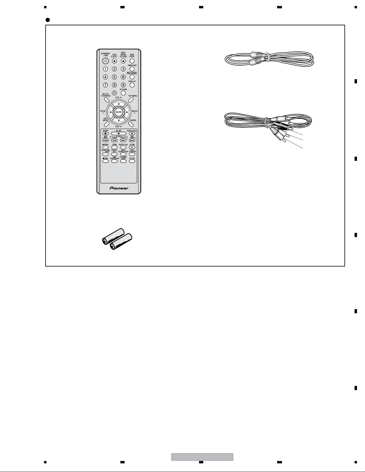
Accessories
• Remote control ×1
(076R0JN020)
• RF antenna cable ×1
(06CPL02006)
• Audio / Video cable(L=1.2m) ×1
(red/white/yellow)
(06CPBA2003)
• Warranty Card
• Operating Instructions
A
B
Red
White
Yellow
C
• Dry cell batteries ×2
(AAA/R03)
D
E
56
DV-PT100-S
F
7
7
8
Page 8
1234
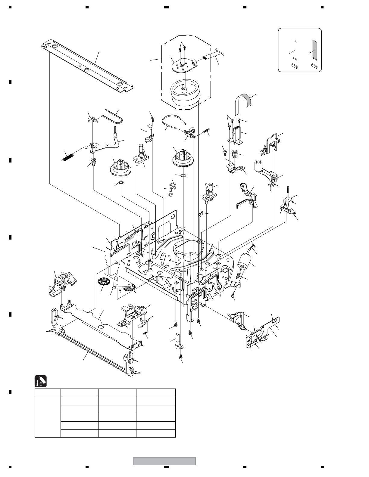
2. EXPLODED VIEWS AND PARTS LIST
NOTES:
A
Parts marked by "NSP" are generally unavailable because they are not in our Master Spare Parts List.
The mark found on some component parts indicates the importance of the safety factor of the part.
Therefore, when replacing, be sure to use parts of identical designation.
Screws adjacent to mark on product are used for disassembly.
For the applying amount of lubricants or glue, follow the instructions in this manual.
(In the case of no amount instructions, apply as you think it appropriate.)
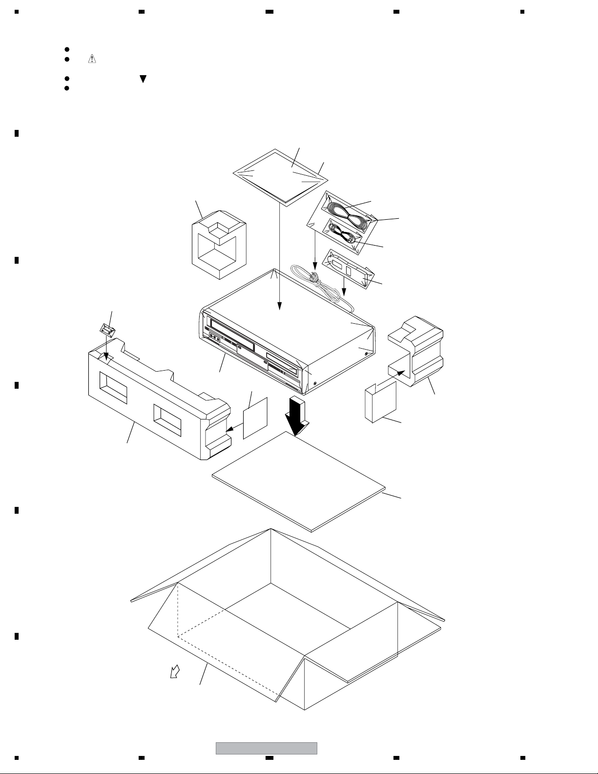
2.1 PACKING
B
C
14
6, 8
10
2
13
7
12
11
1
D
E
3
9
2
15
5
FRONT
F
8
1234
4
DV-PT100-S
Page 9

5678
PACKING parts List
No. Description Part No.
Mark
1 Gift Sheet 791WHA0100
2Package,Back 792WHAA117
3Package,Front 792WHA0558
4 Gift Box 793WCDC541
5Pad,Flat 795WCA0674
6 Instruction Book Kit (English) J2E51401A
7Poly Bag (185x270xT0.04) Y817041000
8 Guarantee Card J2D30902A
9Pad Type : B 795WCAA224
10 Polybag,Instruction JB5UD200
A
11 Remote Control 076R0JN020
12 RF Antenna Cable 06CPL02006
13 Audio/Video Cable 06CPBA2003
NSP 14 Dry Cell Battery(AAA/R03) 1412004008
15 Pad Type : A 759WCAA223
B
C
D
56
DV-PT100-S
E
F
9
7
8
Page 10
1234
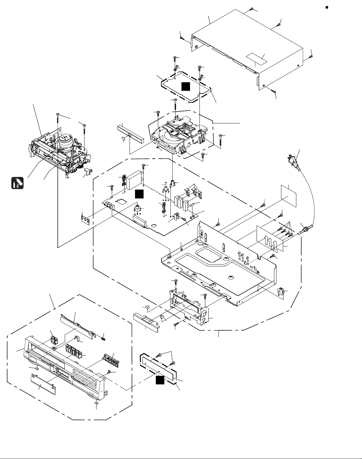
2.2 EXTERIOR SECTION
50
43
50
50
A
Refer to
"2.3 DECK ASSY (TOP SECTION)"
"2.4 DECK ASSY (BOTTOM SECTION)".
B
C
6
Adhesive
Y113031000
46
42
39
47
33
24
25
B
29
55
47
36
53
1
32
53
32
50
A
33
30
44
31
51
41
37
48
PCB130
(DVD PCB ASS'Y)
55
14
2
52
5
Refer to
"2.5 DVD MECHA ASSY"
51
54
50
54
34
49
11
11
22
35
49
C
47
27
47
53
PCB270
47
26
40
PCB010
(VCR PCB ASS'Y)
3
D
7
10
16
(1/2)
8
E
20
9
13
16
19
17
(2/2)
12
27
28
(OPERATION PCB ASS'Y)
20
F
Page 11

>
5678
EXTERIOR SECTION parts List
No. Description Part No.
Mark
1DVD PCB Assy (PCB130) A2E514X130
2 VCR MT PCB Assy(PCB010) A2E514X010
3
4• • • •
5DVD MECHA Assy A2E504X650
6 DECK Assy A2E504X420K
7Front Cabi Assy 7A701A279A
8 Cabinet, Front 701WPJC889
9 Plate, Display 711WPDA591
10 Flap, VCR 712WPJC092
OPERATION PCB Assy(PCB270)
A2E514X270
No. Description Part No.
Mark
49 Screw (3x8) 810923080U
50 Screw (3x6) 8109K3060U
51 Screw (3x33R) 8154D3033U
52 Screw (3x4) 810713040U
53 Screw (2.6x8) 811022680U
54 Screw (2.6x6) 810722660U
55 SEMS (screw 3x8) 810F13080U
A
>
11 AC Cord & Bush (CD501) 1209614920
12 Glass, LED-DVD 713WPA0194
13 Glass, LED-VCR 713WPA0193
14 Fuse (F501 : 2.5A)51MS025L 081PC2R505
15 • • • •
16 Button, Frame_VCR 738WPBA107
17 Button, Frame_DVD 738WPBA108
18 • • • •
19 Spring, Flap 743WKA0042
20 Cushion, Leg 800WFAA015
21 Bottom Cabi Assy 7G7610007A
22 Plate, Bottom 702WSA0216
23 Angle, Center 761WSA0175
24 Plate Tray_Front 712WPBA076
25 Sheet DVD 7235630010
26 Angle Front 761WSAA025
27 Cushion 65TS10-10 8965TS1010
(10 x 20 x 25)
28 Holder, Disc 761WPA0296
29 Holder, Deck 701WPA0686
30 Holder, Deck 701WPA0751
B
C
D
31 Heat Sink IC A023 763WSAA023
32 Spring, Earth 753WUA0065
33 Holder, End Sensor 85OP700038
34 Sheet, Rating 722631A001
35 Sheet, Jack 7230007787
36 Sheet, Caution 726000A073
37 Shield, COMPO 752WSA0290
38 • • • •
39 Shield, 3Pin Jack 752WUAA001
40 Holder, DVD (BR) 761WPA0261
41 Holder, DVD (BL) 761WPA0321
42 Holder, Deck Top 761WPA0262
43 Cabinet, Top 702WSA0212
44 Fiber Washer (3 x 3.2 x T0.5) 800WF00004
45 • • • •
46 Screw (3x29) 8109130B9U
47 Screw (3x7) 810923070U
48 Screw (3x10) 8109I30A0U
56
DV-PT100-S
E
F
11
7
8
Page 12
1234
2.3 DECK ASSY (TOP SECTION)
A
34
49
40
41
35
NON-CONTACT
SIDE
CONTACT SIDE
42
25
24
46
48
B
38
27
29
47
28
10
20
26
19
22
52
11
18
52
8
C
23
AB
AB
AB
AB
6
14
D
21
7
13
AA
AB
AD
AB
AB
AC
15
AB
AB
AC
AB
AB
AB
AB
AB
AB
16
AE
AE
AB
12
51
33
51
51
E
17
AE
53
AE
To VCR MT PCB Assy
CP102
48
37
5
4
3
50
31
AE
AE
AE
32
1
2
AA
9
AA
AA
AA
36
39
AE
AE
30
AE
AE
Class Part No. Part Name Mark
Grease
Y315061000 G-555G AA
NOTE: Applying positions AA, AB, AC, AD and AE for the
grease are displayed for this section.
Check if the correct grease is applied for each position.
Y315071000 MG-33 AB
Y31D011000 FG-84M AC
Y315041000 FL-721 AD
F
12
Y315141000 G-313Y AE
DV-PT100-S
1234
Page 13

>
>
5678
DECK ASSY (TOP SECTION) parts List
No. Description Part No.
Mark
1 Pinch Roller Block (VA) 85OA400240
2 AHC Assy 85OA500026
3Worm 85OP600581
4 Base, AC Head 85OP500083
5 Spring, AC Head 85OP800324
6 Main Chassis Assy 85OA000516
7Arm Idler Assy 85OA200090
8 Inclined Base T Unit 3S 85OA400223
9 P5 Arm Assy 2 85OA400232
10 Tension Arm Assy 2 85OA400235
No. Description Part No.
Mark
50 Screw/Washer (A) (M3x4) 810A130404
51 Screw/Washer (A) (M2.6x5) 810A126504
52 Polyslider Washer 82Q264713N
53 Screw (Bind 2.6x6) 8107226604
A
11 Inclined Base S Unit 85OA400231
12 Spring, Locker 85OP800367
13 Cass, Holder 85OP900736
14 Cass, Side L 85OP900748
15 Cass, Side R 85OP900749
16 Locker, R 85OP900739
17 Link Unit 85OA900228
18 Post, Cass Guide 85OP000496
19 Reel, S (S) 85OP200316
20 Reel, T (S) 85OP200317
21 Gear, Idler 85OP200308
22 Holder, Tension 85OP400492
23 Cap. P4 85OP400520
24 Band, Tension 85OP400542
25 Connect, Tension 85OP400533
26 Arm, Brake T 85OP600573
27 Band, Brake T 85OP600584
28 Spring, Tension 85OP800322
29 Spring, Brake T 85OP800360
30 Lever, Link 85OP900743
31 Lever, Flap 85OP900744
32 Cass, Opener 85OP900745
33 Reflector, LED 85OP700035
34 Bracket, Top 3V 85OP900746
35 Cord Jumper (CD1501) 122H071704
B
C
D
36 Cord Jumper (CD1502) 122Y021902
37 Head (Audio Control)(H5001) 1523Q91004
38 Head (Full Erase)(H5002) 1543Q02014
39 Motor, Loading (M101) 1596S98001
40 Micro Motor (M2003) 1589S11020
41 Cylinder Unit Assy (UN4001) A2D312H500
42 Cord Jumper (CD102) 122T041508
43 • • • • •
44 • • • • •
45 • • • • •
46 Screw (2.6x8) 8107226804
47 Screw (2.6x4) 8107226404
48 Screw (M2x6) 8102120604
49 Screw (2.6x6) 8109126604
56
DV-PT100-S
E
F
13
7
8
Page 14
1234
2.4 DECK ASSY (BOTTOM SECTION)
A
1
21
20
22
B
19
22
AA
12
24
C
3
AA
AB
11
AA
14
AA
22
AA
AA
17
18
AD
AA
AA
AA
13
AA
AA
9
AA
AA
5
AA
4
AB
16
7
AA
15
D
6
AA
AB
AB
AB
AB
AB
AB
AB
AB
2
AA
23
8
10
E
Class Part No. Part Name Mark
Grease
Y315061000 G-555G AA
NOTE: Applying positions AA, AB, AC, AD and AE for the
grease are displayed for this section.
Check if the correct grease is applied for each position.
Y315071000 MG-33 AB
Y31D011000 FG-84M AC
Y315041000 FL-721 AD
F
Y315141000 G-313Y AE
14
DV-PT100-S
1234
Page 15

>
5678
DECK ASSY (BOTTOM SECTION) parts List
No. Description Part No.
Mark
1 Belt, Capstan (S) 85OP200290
2 Main Chassis Assy 85OA000516
3 Clutch Assy 85OA200089
4 Loading Arm S Unit 85OA300065
5 Loading Arm T Unit 85OA300066
6 Gear, Clutch 85OP200311
7 Gear, Coupling 85OP200312
8Lever, Clutch 85OP200313
9 Gear, Main Loading 85OP300194
10 Lever, Tension 85OP400490
A
11 Cam, Pinch Roller 85OP600577
12 Cam, Main 85OP600578
13 Rod, Main 85OP600579
14 Gear, Joint 85OP600582
15 Spring, Coupling 85OP800355
16 Spring, Ring 85OP800356
17 Holder, Capstan 85OP400549
18 Cord Jumper (CD1501) 122H071704
19 Cord Jumper (CD1502) 122Y021902
20 Capstan DD Unit (M2001) 1510S98042
21 Screw (2.6x4) 8107226804
22 E-Ring (3.0) 83ETW30000
23 Screw (2.6x6) 8109126604
24 Polyslider Washer (CUT) 82P184505N
B
C
D
56
DV-PT100-S
E
F
15
7
8
Page 16
1234
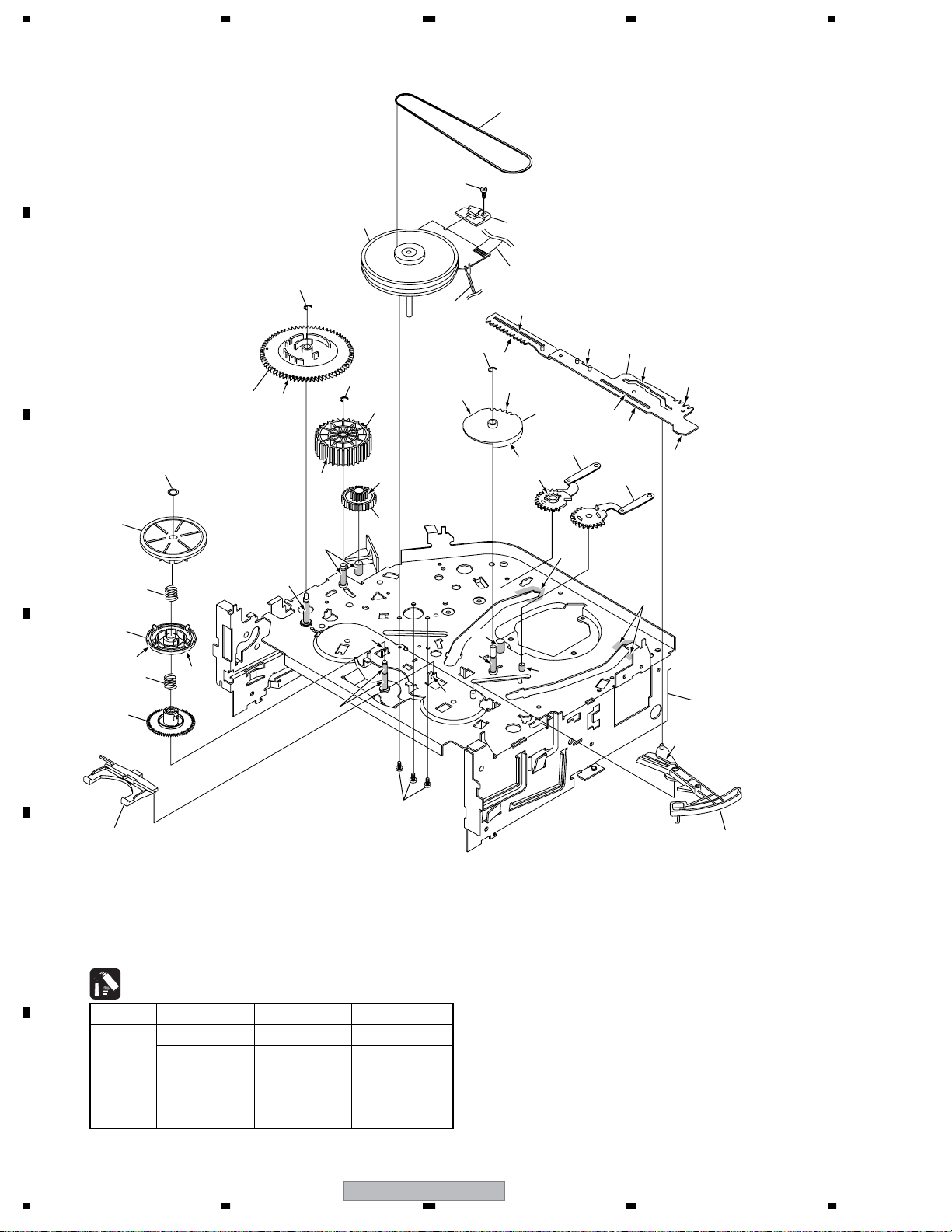
2.5 DVD MECHA ASSY
A
B
34
15
9
AA
18
Cannot supply separately.
If the repair is needed, replace the
LOADER SUB ASS'Y.
11
AA
AA
14
AA
21
AA
AA
AB
AA
C
12
AB
28
30
D
PCB640
AA
CD2301
33
29
E
6
31
(SW PCB ASS'Y)
D
8
E
17
8
CD2001
16
22
24
32
10
2
5
20
4
3
1
PCB610
(LOADING MOTOR PCB ASS'Y)
7
CD2302
Do not replace the parts. Because,
minute adjustments are needed if
this condition is disassembled
further more.
If the repair is needed, replace the
DVD MECHA ASS'Y.
AA
23
19
13
NOTE:
CLASS
GREASE G-555G
F
16
1234
PART NO.
Y315061000
Y315121000
PART NAME
SF-112
MARK
AA
AB
DV-PT100-S
Applying positions AA and AB for the grease
are displayed for this section.
Check if the correct grease is applied for each
position.
Page 17

5678
DVD MECHA ASSY parts List
No. Description Part No.
Mark
NSP 1 Loading Motor PCB Assy A2D801X610
2• • • •
3 Loading Motor Assy 1596S18002
4 Motor Pulley 92P100097A
5 FEED Motor 1515S98002
6 Cord Cable (24P)(CD2001) 122H0O1901
7 Cord Jumper (CD2302) 122H052601
8 Insulator (F) 92P200013A
9 Belt Loading 92P200012A
10 Insulator (R) 92P200014A
A
11 Frame main 92P100091A
12 Tray 92P100100A
13 Holder Traverse 92P100109A
14 Gear Pulley 92P100095A
15 Gear Main 92P100096A
16 Gear Middle 92P100108A
17 SW PCB Assy (PCB640) A2E220T640
18 Clamper Plate 92P000014A
19 Loader SUB Assy 92SBB0020A
20 Clamper 92P100094A
21 Screw (M1.7x3) 814011730U
22 Screw (M1.7x2.3) 814011723U
23 Rack Loading 92P100093A
24 Gear Motor 92P100088A
25 • • • •
26 • • • •
27 • • • •
28 Cord Jumper (CD2301) 122H062102
29 Switch (SW1) 0515S32002
30 Push Switch (SW2) 0500101037
31 Screw (2.6x8) 811022680U
32 Screw (2x8) 816112080U
33 Screw (Bind 2x8) 811022080U
34 DVD MECHA ASSY A2E504X650
B
C
D
56
DV-PT100-S
E
F
17
7
8
Page 18
1234
2.6 WIRING CABLE
A
TU301
VCR PCB
CP102
CD102
J8001
J8006
OS8001
J8007
AC IN
J8008
CD501
S501
S502
B
C
D
CP103
TP101
TP701
TP3002
TP3001
J8003
* All cables are ASSY parts.
DVD DECK
J8004
FE HEAD
J8005
C
AC HEAD
B
OS651
CP681
OPERATION PCB
V651
CP8001
CP501
CD681
CD501
CP8101
CP651
CD8001
CP2603
CP2602
A
CD4002
DVD PCB
CD2001
E
CD2301
CD2302
F
18
DV-PT100-S
1234
CP2601
Page 19
5678
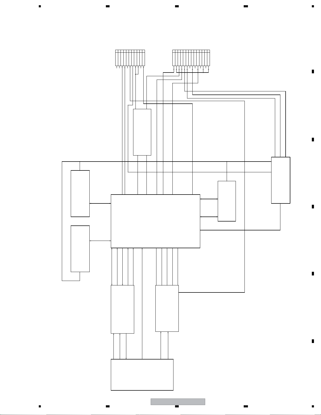
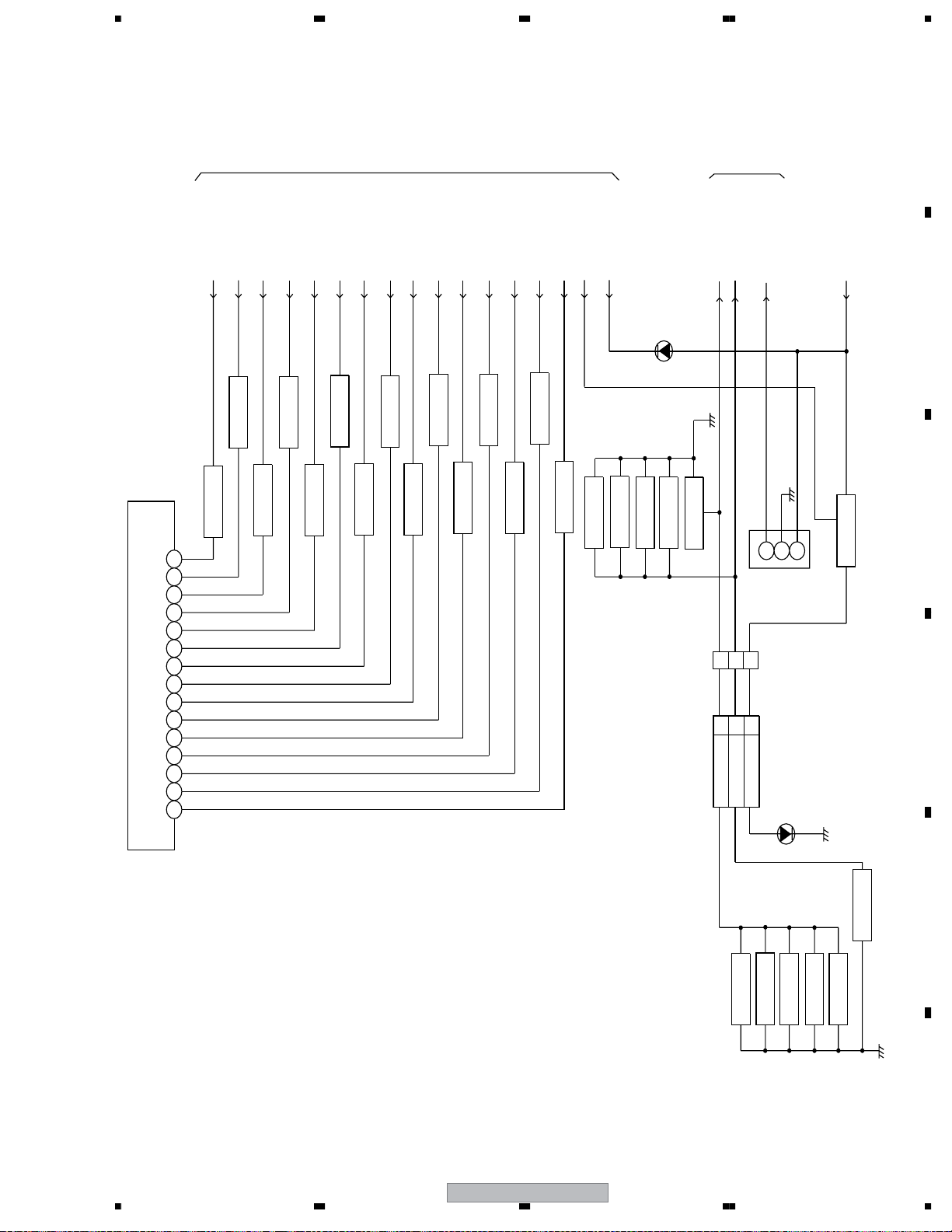
3. BLOCK DIAGRAM AND SCHEMATIC DIAGRAM
3.1 BLOCK DIAGRAM
3.1.1 DVD BLOCK DIAGRAM
1
AUDIO-L
2345678
GND
GND
U(B)
V(R)
CVBS
GND
1
2345678
RX
TX
GND(M)
GND(D)
GND(D)
CD4002
CU2B2201
P.CON+9V
FROM/TO POWER
P.CON+A5V
UNREG+3.8V
9
10
GND(A)
UNREG+3.8V
9
Y(G)
V SW
IMSA-9604S-14F
DVD-H
1011121314
ZERO
DVD RESET
AUDIO-R
GND
11
SPDIF
CP8101_2
FROM/TO
TUNER/JACK
A
B
IC4005
SDRAM 64M
SDA0~SDA11
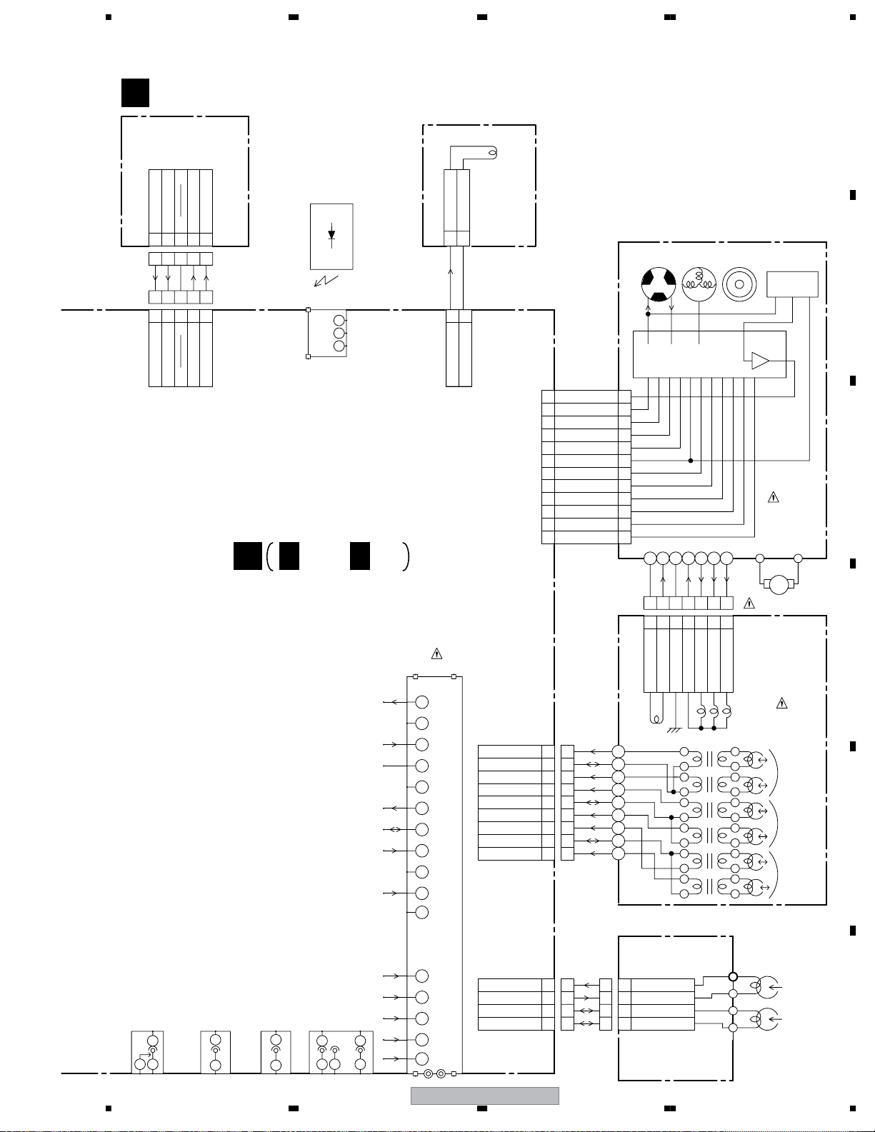
HY57V161610ETP-7
HD0~H120
IC4007
FLASH 8M
SST39VF800A-70-4C-EK-D
SDD0~SDD15
HA0~HA20
FNN,FNP
VBIASS0,S1
AAF_CE,FE,TE,PI
RFA_SDEN,DATA,SCLK
IC4003
SI-3007KWM-TL
REG+3.3V/+1.9V
3.3V
1.9V
W/DSP
MPEG Decoder
DEFECT,LINK,MIRR,LDON
W/u-CON
W/Video Encorder
SPDL_SENS
SPINDLE,SLED_PWM
DAC A,B,C,D
IC4001
TRACK,FOCUS_PWM
(Vaddis6V)
ZR36762PQCG_V
S MUTE
ADC IN 5,6,7
22
I CLKI DAT
IC4002
EEPROM
S-24C04BFJ-TB
AMCLK
ASDATA0
DVD AUDIO L
DVD AUDIO R
IC8502
STEREO DAC
ALRCLK
ABCLK
C
PCM1753DBQR
D
HOME,TIN SW ,TOUT SW
IC2301
LA6565
Moter Driver
TR+/-,FO+/-
SPDL+/-,SLED+/-
Sled Moter
READ CHANNEL
RF
A,B,C,D,E,F
DM3
DVD LOADER
IC2601
ZR36708TQC
CD,DVD,LD
Pick up
Loading Moter
Spindle Moter
DV-PT100-S
56
E
F
19
7
8
Page 20
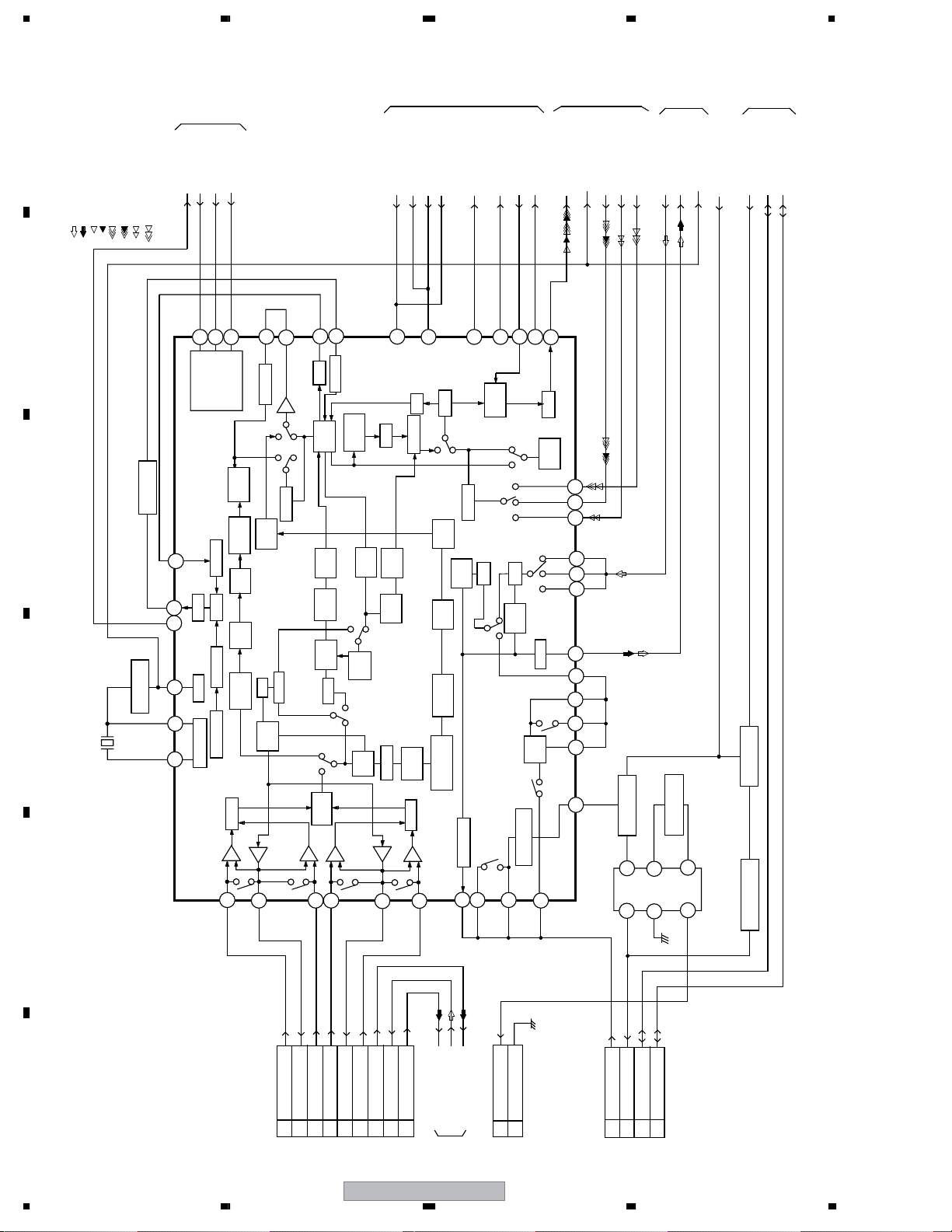
1234
3.1.2 Y/C AUDIO / CCD / HEAD AMP BLOCK DIAGRAM
H. AMP_SW
C. ROTARY
H. SW
58
57
MUTE
AUDIO
C ROT
1/2
Y/C MIX
AMP
B.D.
PB
FM-EQ
H.SW
H
L
SYSCON
AUDIO_MUTE-H
RF SW IN
FBC
R
P
SUB
LPF
LINE
FM
DEM
DOUBLE
LIM
PB
PHASE-EQ
REC AMP
A
RECORD LUMINANCE SIGNAL
PLAYBACK LUMINANCE SIGNAL
TUNER VIDEO SIGNAL
RECORD COLOR SIGNAL
PLAYBACK COLOR SIGNAL
AUDIO SIGNAL (PB)
AUDIO SIGNAL(REC)
SYSCON
Y/C_CLK
Y/C_CS
4FSC
Y/C_DATA
PLAYBACK VIDEO SIGNAL
B
34
21
P
P
Y-LPF
CONV
C-LPF
AMP
36
VCA
CLAMP
R
YNR/
COMB
R
3.58M
BPF2
Main
CONV
B-UP
AMP
GCA
R
P
L
H
H.AMP
SW
H.AMP SW/
NC1
N.L.
DEEM
PB
3.58M
BPF1
KIL
P
R
ACC
AMP
P
R
FM
AGC
DELAY
DECODER
DETAL
ENH
NL
EMPHA
WC
DC
FM
MOD
REC
FM-EQ
H.SW
H
L
22
CLAMP
V/I
KIL
AGC
555453
SERIAL
BUFFER
C
D
X101
Q107
37
CLAMP
39
OUT
43
DRIVER
41
BUFFER
Q109
3.578545M Hz
PULL
49
VX01
TIMMING CCD
50
ENV. DET
59
ENV DET
Chara
V-AGC
LPF
AMP
C.SYNC
COMP
DUMMY_V. SYNC
24
60
25
OUT
CONP
INS.
R
P
ALC
R
ALC
DET
P
EQ
AUTO BIAS
TUNER/JACK
Y/C_VIDEO_OUT
26
6dB
SYNC
SEP
28
30
32
10
MUTE
3
4
AMP
PB.EE
11
FSC
80
2
5 78 76
FRONT_V_IN
TUNER_V
DVD V OUT
BIAS CTL
Q105
2
HI-FI/DEMODU
LATOR
FSC
TO_NORMAL_A
FROM_NORMAL_A
BIAS OSC
Q104
1
3
SYSCON
POWER
V.REC_ST-H
P. CON + 5V
SW
Q103
CTL+
CTL-
7
8
67
Y/C/AUDIO/CCD/HEAD AMP IC
IC101
E
LA71206M
66
F
20
EP/LP-CH2 (L)
EP/LP_COM
2
1
CP101
65
72
SP-CH1 (R)
SP-CH2 (L)
EP/LP-CH1 (R)
SP_COM
5
3
4
6
CYL
73
HF2 (L)
HF_COM
HF1 (R)
7
8
9
HI-FI/DEMODU
DV-PT100-S
9
74
HF1
HF2
HF_COM
CP103
LATOR
FE HEAD
6
FE HEAD (HOT)
FE HEAD (GND)
2
1
L101
COIL, BIAS OSC
5
CTL+
AUDIO PB
AUDIO REC
2
3
4
CP102_1
HEAD
AUDIO
CONTROL
6
CTL1
4
AUDIO PB SW
Q101, Q102
1234
Page 21
5678
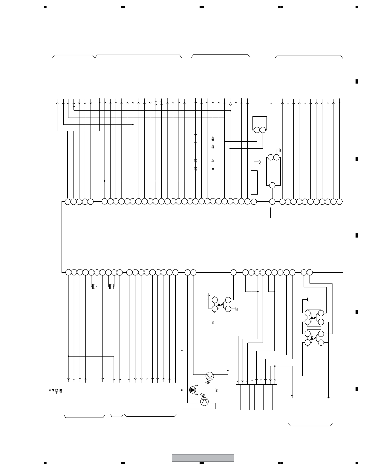
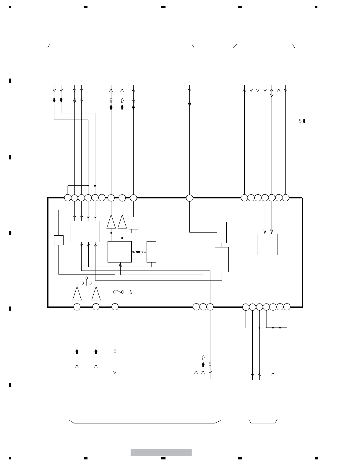
3.1.3 SYSTEM CONTROL BLOCK DIAGRAM
SYSTEM CONTROL BLOCK DIAGRAM
C.SYNC
111
DUMMY_V.SYNC
109
H.SW
105
Y/C/AUDIO/
CCD/HEAD AMP
Y/C CS
C.ROTARY
AUDIO_MUTE-H
H.AMP_SW
95
93
99
100
ENV.DET
V.REC_ST-H
3
24
96
HIFI/
DEMODULATOR
IIC_DATA
IIC_CLK
AUDIO_MUTE-H
REC_MUTE_H
82
22
HIFI_ENV.DET
32
ST_SELECT
HIFI_H.SW
31
106
4FSC
CTL+
CTL-
4
Y/C_DATA
54
COMP
Y/C_CLK
53
101
AV_SW1
39
92
SW_V_ OUT
AFT-S.CURVE
POWER_MUTE-L
87
33
17
TUNER/JACK
VIDEO_OUT
TV/VCR
IIC_CLK
19
61
86
SYS_MUTE
IIC_DATA
VIDEO_MUTE-H
40
88
62
POWER
RF_CH_SW
EEPROM
IC3099
SCL
6
SW
REC SAFTY
94
35
AT+5V
S-24C02BFJ-TB
SDA
5
3
2
RESET
SYSTEM
IC3003
PST3231NR
1
77
SEG 10
SEG 9
73
71
OPERATION/
DISPLAY
SEG 7
SEG 8
68
SEG 6
3G/TV/VCR_LED
4G/TIME SHIFT_LED
50
66
51
SEG 3
SEG 4
SEG 2
5G/CB/BS_LED
59
58
52
60
A
B
C
4FSC IN
HIFI ENV
REC_MUT_H
POWER ON-L
DVD_POWER_CTL
SYSCON/TIMER/SERVO
IC3001 OEC0138A
45
41
RECORD LUMINANCE SIGNAL
PLAYBACK LUMINANCE SIGNAL
RECORD COLOR SIGNAL
PLAYBACK COLOR SIGNAL
DVD_POWER_CTL
VCR_POWER_ON-L
HIFI H.SW
POWER FAIL
RX
37
65
RX
POWER_FAIL
POWER
ST SELECT
OSC 2
OSC 1
TX
64
78
80
X1001
10MHz
TX
C.SYNC
X1
75
X3002
VIDEO H.SW
DUMMY V.SYNC
X2
76
32.768KHz
DVD_POWER_LTL
TUNER/JACK
Y/C CS
C.ROTARY
1G/VCR/T-REC LED
DVD/RESET
48
44
DVD RESET
1G/VCR/T-REC_LED
H.AMP SW
V.REC ST-H
AUDIO MUTE-H
SEG1
VCR LED
SEG5
63
47
55
SEG_5
SEG_1
VCR_LED
OPERATION/
CTL(-)
V ENV
CTL(+)
KEY-B
DVD LCD
2G/DUB/REC LED
49
29
46
KEY-B
DVD_LED
2G/DUB/REC_LED
DISPLAY
Y/C DATA
Y/C CLK
KEY-A
30
KEY-A
COMP
REM IN
43
POWER
AT 5.2V
REM_IN
AV SW1
SYNC DET
BOT-H
25
CV IN1
EOT-H
26
CENT LED
D3001
CV OUT
AFT S.CURVE
POWER MUTE L
P. CON+5V
1
2
EOT SENSOR
Q3006
BOT SENSOR
Q3008
VCR-H
IIC CLK
IIC SDA
REEL SENS
Q3002
3
4
AT+5.2V
SYS_MUTE
RF_CH_SW
VIDEO MUTE H
CYL SPEED UP
REEL-T
42
103
LDM CTL
CYL DRIVE
CYL FG/PG
11
10
12
CP3001
TAB SW
DFG/PG
DRUM PWM
104
107
CAP CTL
I LIMIT
9
5
DD UNIT
CAPSTAN
CAP FULL
LD M CTL
97
102
CAP.M F/R
CAP FG
1
4
RESET
CAP LIMIT
CAP PWM
108
CAP VCO
LD/CY_VCO
8
2
SEG 10
84
SEG 9
SEG 8
CAP FG
CAP FWD-L
9
98
AT+12.6V
SEG 7 67
SEG 6
MS SEN-A
28
1
2
1
2
5G/CB/BS LED
3G/TV/VCR LED
4G/TIME SHIFT LED
MS SEN-B
27
MS_SEN A
Q3005
4
3
4
3
MS_SEN B
Q3004
POWER
SEG 2
SEG 3
P. CON +5V
SEG 4
D
E
F
56
DV-PT100-S
21
7
8
Page 22
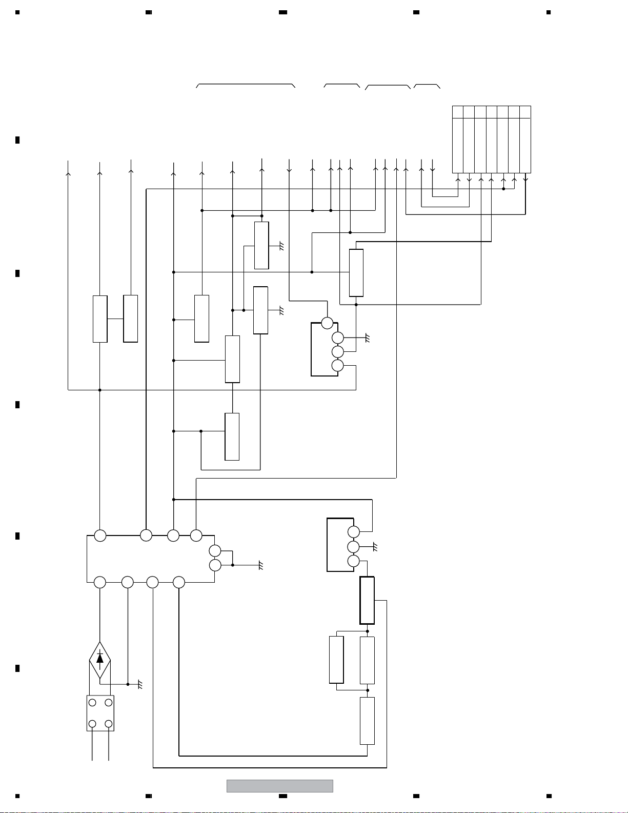
1234
3.1.4 REGULATOR BLOCK DIAGRAM
A
SYSCON
SYSCON
TUNER/JACK
OPERATION/DISPLAY
SYSCON
HIFI/
DEMODULATOR
Y/C/AUDIO/
CCD/HEAD AMP
TUNER/JACK
SYSCON
3
CP501
DVD
4
6
9
7
8
11
AT+12.6V
P.CON+12V
VCR POWER ON-L
AT+5.2V
P.CON+5V
POWER FAIL
AT+5V (M-CON)
DVD POWER CTL
P.CON+5V
P.CON+5V
AT+5.2V
P.CON+9V
P.CON+5V
AT+5.2V
+32V
SPDIF
RX
TX
TX
RX
P.CON+9V
P.CON+5V
UNREG+3.8V
SPDIF
UNREG+3.8V
B
SW.
POWER FAIL
Q514
SW.
P.CON 5V
Q505
SW
Q509
P.CON SW
C
P.CON+12V
Q510
P.CON+5V
Q503
SW.
M-CON+5V
Q504
M-CON
Q506
SW.
POWER FAIL
Q513
SW.
9VREG
POWER SW.
IC502
KIA7809API
4
3
2
1
D
1
2
3
VOLTAGE
CTL. IC
T501
11
2
13
7
6
15
14
12
10
4
IC501
TL431AILP
E
PHOTO
COUPLER
IC503
D505, D506
D502, D503
CONTROL
Q507
F
22
L501
AC IN
DV-PT100-S
Q502
Q501
CONTROL
SW.
1234
Page 23
5678
3.1.5 OPERATION / DISPLAY BLOCK DIAGRAM
A
3
1
2
6
4
5
5G/CS/BS_LED
Q652
5G SW
Q651
SEG10
SEG9
SEG10 SW
SEG9 SW
Q653
4G/T_SHT_LED
4G SW
Q654
Q655
SEG7
SEG8
SEG7 SW
Q656
SEG8 SW
Q657
SEG5
SEG6
SEG5 SW
Q658
SEG6 SW
SYSCON
3G/TV/VCR_LED
Q660
3G SW
Q659
SEG4
2G/DUB/REC_LED
SEG4 SW
Q662
2G SW
Q661
SEG3
SEG2
SEG3 SW
SEG2 SW
Q663
Q664
SEG1
1G/VCR/T-REC_LED
SEG1 SW
1G SW
Q665
DVD_LED
VCR_LED
VCR EJECT
POWER
VCR/DVD
VCR LED
D651
CH UP
SYSCON
CH DOWN
CP651
KEY-A
KEY-B
215
REM_IN
1
2
OS651
POWER
AT+5.2V
B
C
3
DVD LED SW
Q666
897
10
12 11
13
14 15
V651 C02D0M3-A
CP681
1
5
2
KEY-A
KEY-B
DVD LED
DVD LED
D681
D
E
OPEN CLOSE
STOP
REC/OTR
FF/CUE
PLAY
REW/REV
F
56
DV-PT100-S
23
7
8
Page 24
1234
3.1.6 HiFi / DEMODULATOR BLOCK DIAGRAM
A
FRONT_A_IN-L
FRONT_A_IN-R
DVD_A_OUT- L
DVD_A_OUT-R
TUNER/JACK
AUDIO_OUT_L
AUDIO_OUT_R
RF_CONV_A.OUT
SIF OUT
B
C
9
11
78
71
74
12
73
2
80
57
SYSCON
HIFI_H.SW
HIFI_ENV. DET
39
23
IIC_DATA
AUDIO_MUTE-H
IIC_CLK
ST_SELECT
49
40
37
38
REC_MUTE-H
AUDIO SIGNAL (PB)
AUDIO SIGNAL(REC)
17
AMP
ALC
INPUT SW
D
AMP
HIFI AUDIO/H.AMP/DEM IC
IC701
LA72670BM-L-MPB-E
24
AMP
27
26
SW
OUTPUT
MUTE
PNR
DEM
BLOCK
LOGIC
DBX
NOISE
REDUCTION
4
6
51
3
5
54
46
15
32
36
ALC/
AMP
E
HF1
HF2
HF_COM
FSC
AT+5.2V
P.CON+9V
P.CON+5V
TO_NORMAL_A
FROM_NORMAL_A
F
Y/C/AUDIO/CCD
POWER
/HEAD AMP
24
DV-PT100-S
1234
Page 25
5678
3.1.7 TUNER / JACK BLOCK DIAGRAM
RECORD LUMINANCE SIGNAL
PLAYBACK LUMINANCE SIGNAL
AUDIO SIGNAL (PB)
AUDIO SIGNAL(REC)
AUDIO R
J8005
AUDIO L
J8004
TUNER VIDEO SIGNAL
RECORD COLOR SIGNAL
PLAYBACK COLOR SIGNAL
3
2
2
Y/C/AUDIO/CCD
HEAD AMP
FRONT_V_IN
DVD V OUT
FSC
DIGITAL AUDIO SIGNAL (PB)
PLAYBACK VIDEO SIGNAL
Y/C VIDEO OUT
HI-FI/
DEMODULATOR
FRONT_A_IN-L
FRONT_A_IN-R
TUNER_V
DVD_A_OUT-R
AUDIO_OUT_R
AUDIO_OUT_L
DVD_A_OUT-L
RF_CONV_A. OUT
SIF OUT
POWER MUTE_L
TV/VCR
SCL
SYSCON
RF_CH_SW
AFT-S. CURVE
DVD POWER CTL
SYS_MUTE
AV SW1
DVD_RESET
CP8001
5
1
V SW
2
2
3
Y(G)
DVD-H
DVD/VCR SW
IC8005
3
Vcc
DVD
6
5
ZERO
8
AUDIO-L
AUDIO-R
4
DVD RESET
MM1501XNRE
10
V(R)
12
U(B)
A
14
CVBS
B
C
FRONT AV
JACK VIDEO
J8003
REAR OUT JACK
J8001
2
5
3
2
Q8004
Q8003
BUFFER
VIDEO
MUTE SW
OS8001
OPTICAL
4
1
6
MUTE SW
Q8005
MUTE SW
Q8007
D
MUTE SW
Q8006
IC8001
NJM4580M
AUDIO AMP
MUTE SW
Q301
DVD AIDIO L
SW 8001
DVD AIDIO R
VIDE OUT SW
E
AUDIO MUTE
Q8008, Q8009
Q8010, Q8011
2
1
DRIVER
DVD AUDIO
Q8001
Q8012
Y/C SEPA
Y
J8008
Y
U
C
3
4
J8007
Y/U/V OUT
V
2
3
5
VIDEO MUTE H
VIDEO_OUT
SYSCON
56
SW V OUT
+32V
P. CON+12V
SPDIF
P.CON+5V
POWER
TU301
1
5
3
4
8
15
10
DV-PT100-S
2
17
11 SDA
14
12
3
5
J8006
DVD AIDIO OUT
2
F
25
7
8
Page 26
1234
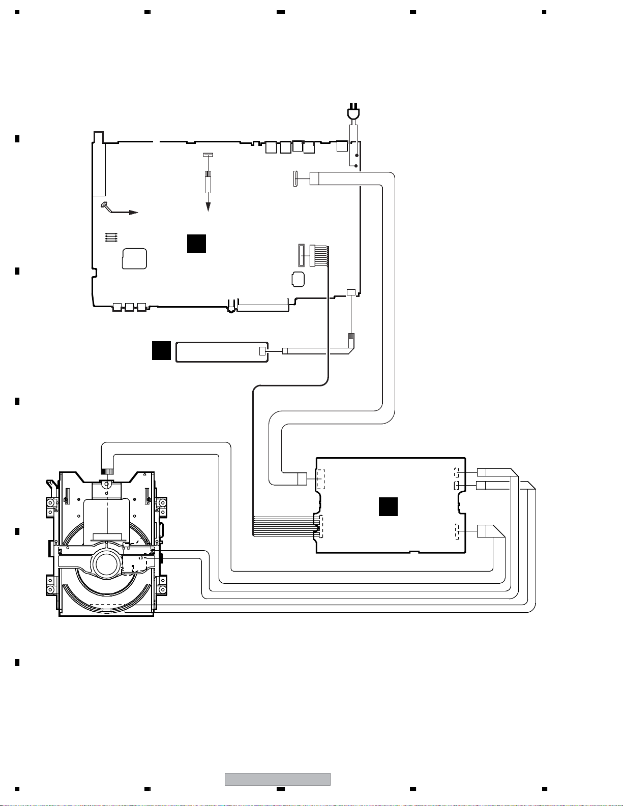
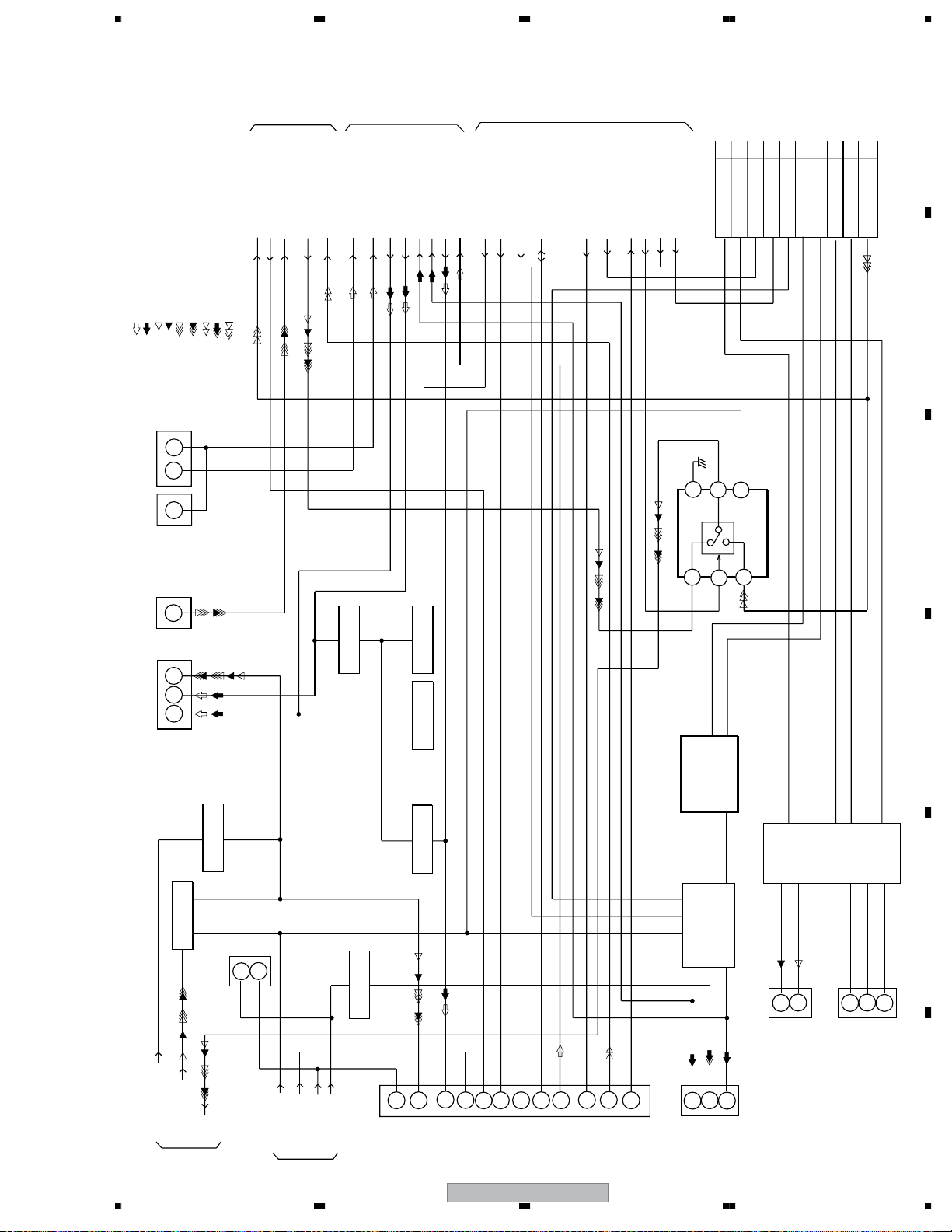
3.2 SW,LOADING MOTOR PCB ASSYS and OVERALL WIRING DIAGRAM
÷
When ordering service parts, be sure to refer to "EXPLODED VIEWS and PARTS LIST" or
A
"PCB PARTS LIST".
÷
The > mark found on some component parts indicates the importance of the safety factor
of the part. Therefore, when replacing, be sure to use parts of identical designation.
÷
: The power supply is shown with the marked box.
DVD MECHA ASSY
(A2E504X650)
B
OPTICAL PICKUP
C
SW PCB ASSY
D
M2601
SPINDLE
JCV9B06
ESE22MH24
SW1
SSS-13-2
MOTOR
SW2
M2602
BCZ3B03
SLED MOTOR
M2603
BCZ3B52
LOADING MOTOR
D
M
M
PICK UP INNER LIMIT SWITCH
M
TT+
FF+
MON(DVD)
NC(SW)
VOL(DVD)
GND(DVD)
LD(DVD)
LD(CD)
VOL(CD)
GND(CD)
MON(COM)
RF
C
B
A
D
F
E
VCC
VREF
GND(PDIC)
CD2301
2H062102
SPINDLE MOTOR (+)
SPINDLE MOTOR (-)
FEED MOTOR (+)
FEED MOTOR (-)
GND(SW)
CD2302
2H052601
SW-2(CLOSE)
GND(SW)
SW-1(OPEN)
LOADING MOTOR(+)
LOADING MOTOR(-)
A
A 1/4 - A 4/4
DVD PCB ASSY (A2E514X130)
FFC
1
2
3
4
5
6
7
8
9
10
11
12
13
14
15
16
17
18
19
20
21
22
23
24
1
2
3
4
5
6
CP2601
1
2
3
4
5
MON(DVD)
6
NC(SW)
7
VOL(DVD)
8
GND(DVD)
9
LD(DVD)
10
LD(CD)
11
VOL(CD)
12
GND(CD)
13
MON(COM)
14
DVD/CDDVD/CD
15
16
17
18
19
20
21
22
23
24
GND(PDIC)
CP2603
1
2
3
4
5
6
CP2602
1
GND(D)
2
3
4
5
TT+
FF+
RF
C
B
A
D
F
E
VCC
VREF
SP1+
SP1SLD+
SLD-
LIMIT SW
SW(GND)
CLOSE
OPEN
LD+
LD-
CD4002
GND(D)
GND(D)
TX
RX
GND(M)
P.CON+9V
P.CON+A5V
UNREG+3.8V
UNREG+3.8V
GND(A)
SPDIF
CP8101_2
V SW
Y(G)
DVD-H
DVD RESET
ZERO
AUDIO-R
GND
AUDIO-L
GND
V(R)
GND
U(B)
GND
CVBS
CP501
1
2
3
4
5
6
7
8
96
10
11
12
13
14
1
2
3
4
5
6
7
P.CON+A5V
8
UNREG+3.8V
9
UNREG+3.8V
10
11
CP8001
1
2
3
DVD RESET
4
5
6
7
8
9
10
11
12
13
14
GND(D)
GND(D)
TX
RX
GND(M)
P.CON+9V
GND
SPDIF
V SW
Y(G)
DVD-H
ZERO
AUDIO-R
GND
AUDIO-L
GND
V(R)
GND
U(B)
GND
CVBS
1
2
3
4
5
6
7
8
9
10
11
CD8001
14
13
12
11
10
9
8
7
6
5
4
3
2
1
FFC
14
13
12
11
10
9
8
7
5
4
3
2
1
1
2
3
4
5
6
7
8
9
10
11
12
13
14
15
16
17
18
19
20
21
22
23
24
6
5
4
3
2
1
5
4
3
2
1
E
F
26
E
D E
LOADING MOTOR
PCB ASSY
FG SENSER
WHITE
BLADE
WIDE
BLACK
AC120V_60HZ
CD501
DV-PT100-S
1234
OPTICAL
OS8001
INPUT
1
VCC
2
3
GND
S502
S501
WHITE
BLACK
YUV OUT
J8007
1
2 345
VIDEO OUT SW
SW8001
H
EE
COMPLS/CVBS
H1H1 H2
Y/C SEPA
J8008
1
2345678
1112131415161718
34
12
56
DVD AUDIO OUT
J8006
4
5
H1
EE
1
23
H1H2
Page 27
5678
OPERATION PCB ASSY
C
(A2E514X270)
GND
KEY-A
DVD LED
54321
CP681
54321
FFC
CD681
54321
54321
KEY-B
CP651
GND
KEY-A
DVD LED
KEY-B
B
VCR PCB ASSY
(A2E514X010)
COMMAND TRANSMITTER
TM601
OS651
Vout
1
2
GND
3
B+
B 1/6 - B 6/6
FULL ERASE HEAD ASSY
FE HEAD (GND)
FE HEAD (HOT)
2
1
H5002
2
1
CP103
FE HEAD (GND)
FE HEAD (HOT)
CP3001
1
2
3
4
5
6
7
8
9
10
11
12
CAP FG
CAP VCO
VCC
CAP.M/F/R
I LIMIT
MOTOR GND
GND
LD/CY VCO
CAP CTL
LDM CTL
CYL FG/PG
CYL CTL
A
HALL
SENSOR
HALL
HALL
IN
VCC
1
2
3
4
5
6
7
8
9
10
11
12
3
2
1
OUT
SWITCH
LOGIC
5
4
MAGNETCOIL
7
6
ROTOR
MAIN
FFC
7
6
5
4
3
2
1
7
6
5
4
3
2
1
MR
FG SENSOR
OGVCC
CAPSTAN DD UNIT
M2001
WHITERED
LM
LOADING MOTOR
M101
B
C
FRONT AV JACK
AUDIO IN R
J8005
E
1
23
HNC
TU301
20
21
17
V.OUT
NC
NC
16
CP101
HF1 (R)
HF COM
HF2 (L)
SP-CH1 (R)
SP COM
SP-CH2 (L)
EP/LP-CH1 (R)
EP/LP COM
EP/LP-CH2 (L)
CP102_1
AUDIO REC
AUDIO PB
CTL+
CTL-
FRONT AV JACK
AUDIO IN L
J8004
E
1
2
H
FRONT AV JACK
VIDEO
JJ8003
E
1
2
H
REAR OUT JACK
J8001
EE
1
2 345
TU 32V
15
SIF OUT
14
13
NC
A.OUT
AFT
12
DATA
11
CLOCK
10
NC
9
NC
8
FSC
7
NC
NC
V.IN
5
4
CONTROL
+B
3
CH
2
1
A.IN
H1H1 H2
18
19
DV-PT100-S
56
M-GND
D-PG OUT
D-PG GND
D-COM
D-W OUT
D-U OUT
D-V OUT
CYLINDER UNIT
D
FPC
CD102
FFC
9
8
7
6
5
4
3
2
1
HEAD AUDIO CONTROL ASSY
H5001
4
3
2
1
4
3
2
1
AUDIO PB
AUDIO REC
CTL+
CTL-
HI-FI HEAD
SP HEAD
EP/LP HEAD
AUDIO
CONTROL
E
F
9
9
8
8
7
7
6
6
5
5
4
4
3
3
2
2
1
1
4
4
3
3
2
2
1
1
27
7
8
Page 28
1234
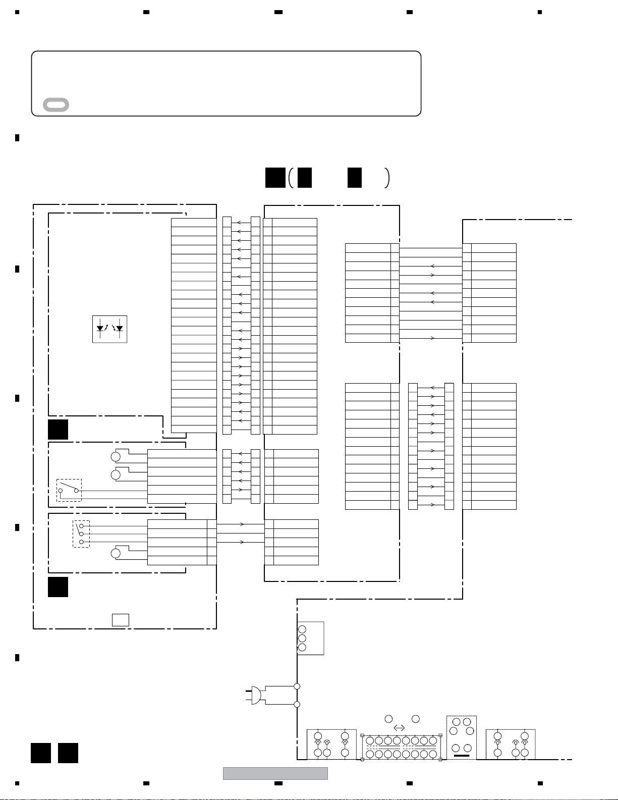
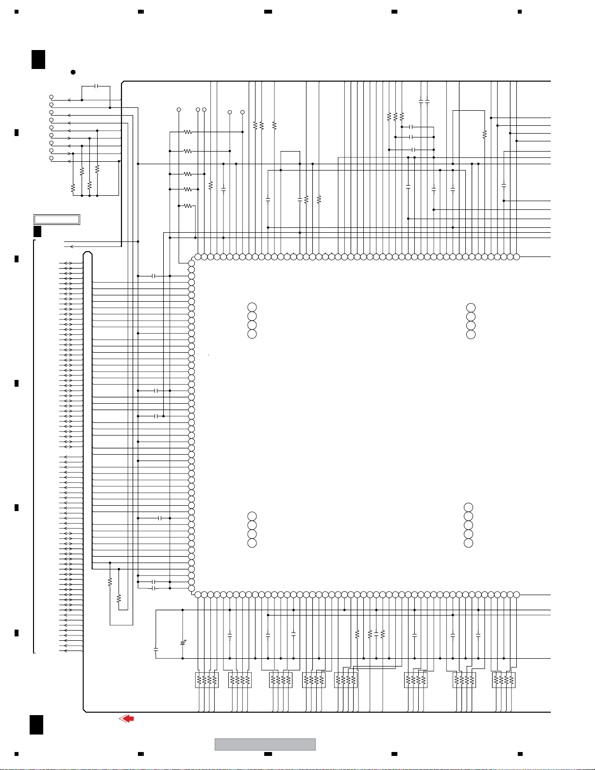
3.3 DVD PCB ASSY(1/4)
A
B
C
D
E
A 1/4
JG001
JG002
JG003
JG004
JG005
JG006
JG007
JG008
JG009
FROM/TO MEMORY
2/4A
GND
P.CON+3.3V
HA0
HA1
HA2
HA3
HA4
HA5
HA6
HA7
HA8
HA9
HA10
HA11
HA12
HA13
HA14
HA15
HA16
HA17
HA18
HA19
HA20
HD0
HD1
HD2
HD3
HD4
HD5
HD6
HD7
HD8
HD9
HD10
HD11
HD12
HD13
HD14
HD15
MEMCS0
RD
WR
SD_A0
SD_A1
SD_A2
SD_A3
SD_A4
SD_A5
SD_A6
SD_A7
SD_A8
SD_A9
SD_A10
SD_A11
SD_D0
SD_D1
SD_D2
SD_D3
SD_D4
SD_D5
SD_D6
SD_D7
SD_D8
SD_D9
SD_D10
SD_D11
SD_D12
SD_D13
SD_D14
SD_D15
RAMCS0#
RAMCS1#
RAMRAS#
RAMCAS#
SD_BA0
RAMDQM
RAMWE#
RAMCLK
DVD PCB ASSY (A2E514X130)
MPEG/MICON/DSP BLOCK
C4038
R4037
R4036
0.01 B
UNREG+3.8V
R4039
4.7K
4.7K
R4038
4.7K
BOOT2
BOOT1
DUPTD1
DUPRD1
DUPTD0
DUPRD0
P.CON+5V
4.7K
HA15
HA16
HA14
HA13
HA12
HD15
HA11
HD7
HA10
HD14
HA9
HD6
HA8
HD13
HD5
HA20
HD12
WR
HD4
HD11
HD3
HA19
HD10
HA18
HD2
HA17
HD9
HA7
HD1
HA6
HD8
HA5
HD0
HA4
RD
HA3
HA2
MEMCS0
HA1
HA0
R4053
1K
R4054
1K
BOOTSEL2
BOOTSEL1
C4008
0.1 F
C4010
0.1 F
C4013
0.1 F
C4014
0.1 F
C4016 0.1 F
C4017 0.1 F
C4077
JG064
FPCRX
R4052
4.7K
R4051
4.7K
R4050
4.7K
R4049
4.7K
R4046
4.7K
3.3
3.3
NC
3.3
3.0
3.0
3.0
3.3
3.3
0
0.5
2.6
0
0
1.9
0
0
0
2.1
2.0
0
3.3
0.6
3.3
2.6
1.8
2.7
2.9
0
0
0.5
0
0
0.6
0
0.6
2.7
2.7
0.6
0.4
5.5
3.3
0.4
3.3
0
0
0
3.1
3.1
3.2
0
3.3
3.3
C4078_1
0.1 F
MIRR
JG065
JG027
SPDL_SENS
FPCTX
FPCCLK
R4072 8.2K
C4001 0.1 F
3.3
0.7
3.3
3.3
4.3
110
SSCRXD
MEMCS(1)
3
4
5
111213141516171819 22021222324
2526272829
30313233343536373839
40414243444546474849
50
5152
1006.3V KA
VDDP
VDDP
MEMAD(15)
MEMAD(16)
MEMAD(14)
MEMAD(13)
MEMAD(12)
MEMDA(15)
MEMAD(11)
MEMDA(7)
GNDP
MEMAD(10)
MEMDA(14)
MEMAD(9)
MEMDA(6)
MEMAD(8)
MEMDA(13)
MEMDA(5)
MEMAD(20)
VDDP
MEMDA(12)
MEMWR#
MEMDA(4)
VDDC
MEMDA(11)
MEMDA(3)
MEMAD(19)
GNDC
MEMDA(10)
MEMAD(18)
GNDP
MEMDA(2)
MEMAD(17)
MEMDA(9)
MEMAD(7)
MEMDA(1)
MEMAD(6)
MEMDA(8)
MEMAD(5)
VDDP
MEMDA(0)
MEMAD(4)
MEMRD#
MEMAD(3)
MEMAD(2)
MEMCS(0)#
MEMAD(1)
MEMAD(0)
GNDP
VDD-IP
RAMADD(6)
VDDP
53 545556 57 58 59660 61 62 63 64 65 66 67 68 69770 71 72 73 74 75 76 77 78 79880 81 82 83 84 85 86 87 88 89990 91 92 93 94 95 96 97 98 99
0.9
0.3
1.001.0
JG028
JG029
IRRCV
FPCSTRB
FPCSTRB
IRRCV
GNDP
ICGPCI/O(7)
ICGPCI/O(6)
RAMADD(1)
RAMADD(7)
VDDP
3.301.0
C4018 0.1 F
DEFECT
RFA_DATA
RFA_SDEN
R4057 100
R4073 100
DEFECT
PWMCO(6)
PWMCO(5)
208
SSCTXD
207
SSCCLK
206
SPINDLEPULSE
205
SLEDPULSE
53
RAMADD(4)
54
RAMADD(3)
55
RAMADD(5)
56
RAMADD(2)
RAMADD(0)
GNDP
RAMADD(8)
0.200.2
RFA_SCLK
R4056 100
3.30003.303.3
VDDPWM
PWMCO(4)
VDDC
RAMADD(10)
1.8
1.900.2
C4019 0.1 F C4002 0.1 F
GND
S
NC
2.9
2.903.3
GNDPWM
PWMCO(3)
RAMADD(9)
GNDC
3.303.1
C4020 0.1 F
SLED_PWM
SPINDLE_PWM
C4003 0.1 F
R4061 3.3K
R4060 1K
NC
0.701.5
1.8
VDDC
GNDC
PWMCO(1)
PWMCO(0)
PWMCO(2)
RAMADD(11)
RAMBA(0)
GNDP
VDDP
RAMCS(0)# RAMBA(1)
0.503.1
AAF_PI
AAF_TE
VBIASS1
VBIASS0
GND
AFE
NC
NC
187188189190191192193194195196197198199200201202203204205206207208
PWMACT(1)
1.7
1.1
000
VBIASS1
GNDAFES
PWMACT(0)
1.8
1.6
VBIASS0
ADCIN(0)
ADCIN(1)
IC4001
ZR36762PQCG_V
MPEG/MICON/DSP
RAMWE#
RAMDQM
GNDPCLK
VDDP
RAMCAS#
RAMCS(1)#
RAMRAS#
0
0.2
0
3.2
3.3
3.2
R4059 100
AAF_FE
AAF_CE
1.7
ADCIN(3)
ADCIN(2)
PCLK
VDDPCLK
1.6
3.3
R4008 100
C4022 0.1 F
LINK
ADCIN_5
ADCIN_6
R4043 10K
R4044 10K
1.5
1.600
ADCIN(5)
ADCIN(4)
RAMDAT(8)
GNDP
2.101.3
R4064 100
ADCIN_7
C4086
C4088
0.01 B
C4089
R4022 10K
0.01 B
C4090
0.01 B
C4004 0.1 F
0
3.3
1.7
ADCIN(7)
ADCIN(6)
VDDAFES
RAMDAT(9)
RAMDAT(6)
RAMDAT(7)
0.8
0.8
3.3
C4023 0.1 F
FNN
FNP
0.001 B
RFINN
RFINP
C4005 0.1 F
1.2
1.2
RFINP
RFINN
GNDAFERF
VDDP
RAMDAT(10)
RAMDAT(5)
1.7
1.3
0.500.9
TRACK_DAC
C4085 0.001 B
C4006 0.1 F
3.3
0.803.3
VDDAFERF
GNDDACDS
DACDRIVE(1)
GNDP
RAMDAT(4)
RAMDAT(11)
1.8
C4024 0.1 F
FOCUS_DAC
VDDDACS
GNDDACPS
DACDRIVE(0)
160
159
158
157
100
101
102
103
104
VDDC
GNDC
RAMDAT(12)
1.400.5
DAC_VIDEO_C
R4001
390 +-1%
1.2
1.20000.9
RSET
C/B/U
GNDDACP
GNDDACBS2
VDDDAC
CVBS/C
CVBS/G/Y
GNDDACD
RAMDAT(14)
GNDP
RAMDAT(1)
RAMDAT(15)
RAMDAT(0)
VDDP
RAMDAT(13)
RAMDAT(2)
RAMDAAT(3)
100
3.3
2.0
0.4
C4025 0.1 F
DAC_VIDEO_D
DAC_VIDEO_A
DAC_VIDEO_B
C4007 0.1 F
1.1
1.2
3.3
1.1
158159160161162163164165166167168169170171172173174175176177178179180181182183184185186
Y/R/V
101102 103
1.500.8
1.2
F
28
A 1/4
NR4001
NR4002
SD_A4
SD_A3
SD_A5
SD_A2
4D03WGJ0101T5E
4D03WGJ0101T5E
SD_A6
DIGITAL AUDIO SIGNAL(PB)
SD_A1
SD_A7
SD_A0
NR4003
SD_A10
SD_A11
SD_A8
SD_A9
4D03WGJ0101T5E
NR4004
RAMCS0#
RAMCS1#
RAMRAS#
SD_BA0
4D03WGJ0101T5E
NR4005
RAMCAS#
RAMWE#
RAMDQM
RAMCLK
SD_D7
SD_D9
4D03WGJ0101T5E
NOTE:THE DC VOLTAGE EACH PART WAS
MEASURED WITH THE DIGITAL TESTER
DURING PLAYBACK.
SD_D8
NR4006
SD_D10
SD_D11
SD_D6
SD_D5
4D03WGJ0101T5E
NR4007
SD_D4
4D03WGJ0101T5E
SD_D12
SD_D13
SD_D3
NR4008
SD_D14
SD_D15
SD_D2
SD_D1
4D03WGJ0101T5E
DV-PT100-S
1234
Page 29
5678
R4002 75 +-1%
R4003 75 +-1%
R4004 82 +-1%
R4005 75 +-1%
0
157
DUPTD1
DUPRD1
VDD-IP
DUPTD0
DUPRD0
GNDP
IDGPCI/O(3)
GPCI/O(34)
ICGPCI/O(5)
GPCI/O(33)
ICGPCI/O(4)
GPCI/O(32)
VDDP
GCLKA
GCLKP
XO
VDDA
RESET#
GNDA
IDGPCI/O(2)
GPCI/O(31)
VID(0)
VID(1)
VID(2)
VID(3)
V SW
D1 2
D1 1
VID(7)
VDDP
STBY-L
GNDP
HSYNC
VDDC
VSYNC
GNDC
AIN
VDDP-A2
AMCLK
GNDP-A2
ABCLK
ALRCLK
GPAI/O
AOUT(0)
AOUT(1)
AOUT(2)
SPDIF
IDGPCI/O(0)
ICGPCI/O(0)
GNDP
GPCI/O(20)
VDDP
105106 107108 109110111 112113 114115 116117118 119120 121122 123124125 126127 128129 130131132 133134 135136 137138139 140141 142143 144145146 147148 149150 151152153 154155 156
104
1.5
100
R4068
SD_D0
GND
476.3V KA
476.3V KA
476.3V KA
476.3V KA
C4069_1
C4068_1
C4067_1
+1.8V
+3.3V
4.7K
R4023
3.3
5.1
3.3
3.3
5.0
0
3.3
0
3.3
0
0
3.1
3.3
0
0
1
R4042
0
1.8
100
3.3
0
3.3
HOME
3.3
3.3
3.3
DJTDO ML
0
DJTDI MC
0
DJTMS MD
0
ICETCK V_SW
3.3
ICETDO
3.3
ICETDI
3.3
SYS_MUTE
3.3
3.3
0
3.3
1.6
3.3
0
3.3
R4024
3.3
4.7K
1.7
0
1.7
1.6
0
NC
0
0
ASDATA1
0
ASDATA2
1.6
0
NC
0
NC
0
0
3.3
C4082
C4027 0.1 F
27MHz
X4001
100BT02701
C4028 0.1 F
TP4007
TP4010
C4030 0.1 F
C4031 0.01 B
STBY_L
TP4015
TP4016
C4026 0.1
0.1 F
C4033 0.1 F
C4032 0.001 B
C4096 0.001 B
C4034 5P CH
1M
R4012
C4035 16P CH
R4019 33
R4020 33
R4021 33
R4047
33
JG066
B4010
FCM2012H-102T04
R4014 4.7K
F
FCM2012H-102T04
1006.3V KA
C4083_1
476.3V KA
C4070_1
C4071_1
C4072 0.1 F
R4018 4.7K
C4079 100P CH
C4029 0.1 F
R4025 220
IAMCLK
R4026 220
IABCLK ABCLK
R4027 220
IALRCLK ALRCLK
R4058 220
R4071
150
B4006
C4073 0.1 F
C4074 0.1 F
4.7K
R4045
DUPTD0
DUPRD0
VR_SEL
TRAY_OPEN
TOUT_SW
TRAY_CLOSE
TIN_SW
R4016
100
C4081 0.1 F
TP4004
TP4006
TP4005
ASDATA0
C4011_1
C4076 0.1 F
C4075 0.1 F
DUPTD1
DUPRD1
SMUTE
RESET
HOME
LDON
I2CDAT
I2CCLK
C4098
10P CH
AMCLK
SPDIF
1006.3V KA
C4012
W817
DUPTD1
FCM2012H-102T04
B4002
B4001
FCM2012H-102T04
B4005
FCM2012H-102T04
TP4008
TP4009
I2CCLK
I2CDAT
C4093
100P CH
C4094 100P CH
DVD-H
P.CON+3.3V
UNREG+3.8V
0.1 F
C4091
B4003
FCM2012H-102T04
B4004
FCM2012H-102T04
R4031 4.7K
R4035
3.2 0 3.33.2
5678
IC4002
S-24C02BFJ-TB
EEPROM IC
IC4003
SI-3007KWM-TL
REG+3.3V 1.9V IC
VO1
1
C4052
JG050
0.1 F
6
2 345
03.35.1
1006.3V KA
C4053_1
RX
P.CON+3.3V
100P CH
4.7K
VCCWPSCLSDA
NCNCNCGND
1234
V_INGNDV_C
3.8 1.9
C4009_1
0000
13
R4070
4716V KA
VO2
C4037
47K
C4015
TP4003
0.1 F
JG051
F
0.1
DUPRD1
RX
M_GND
VCC+9V
P.CON+A5V
P.CON+5V
SPDIF
UNREG+3.8V
FROM/TO AUDIO/VIDEO
SYS_MUTE
DVD-H
V_SW
DAC_VIDEO_A
DAC_VIDEO_C
DAC_VIDEO_B
DAC_VIDEO_D
ASDATA0
ABCLK
ALRCLK
AMCLK
MD
MC
ML
RESET
P.CON+5V
GND
GND
KA
47
C4084_1
C4097 0.01 B
C4036 0.1 B
6.3V
C4065 0.01 B
L4001
2.2uH
0305
JG011
JG016
4/4A
FROM/TO RF AMP/DSP
TRAY_OPEN
TRAY_CLOSE
HOME
SPDL_SENS
TOUT_SW
TIN_SW
RFA_SDEN
RFA_DATA
RFA_SCLK
AAF_CE
AAF_FE
AAF_TE
AAF_PI
VR_SEL
FNN
FNP
VBIASS0
VBIASS1
DEFECT
LINK
MIRR
LDON
SMUTE
TRACK_DAC
FOCUS_DAC
SPINDLE_PWM
SLED_PWM
P.CON+A5V
P.CON+3.3V
VCC+9V
P.CON+5V
ADCIN_7
ADCIN_6
ADCIN_5
M_GND
D
GND
CH
C4092 100P
JG059
JG017
C4080
JG018
JG015
JG012
JG014
C4066
1B
0.01 B
FROM/TO POWER
CD4002
CU2B1101
GND(D)
GND(D)
TX
RX
GND(M)
P.CON+9V
P.CON+A5V
UNREG+3.8V
UNREG+3.8V
GND(A)
SPDIF
GND
JG010
1
2
3
4
5
6
7
8
9
10
11
A
B
C
3/4A
D
E
CP501
B 6/6
F
56
DV-PT100-S
A 1/4
29
7
8
Page 30
1234
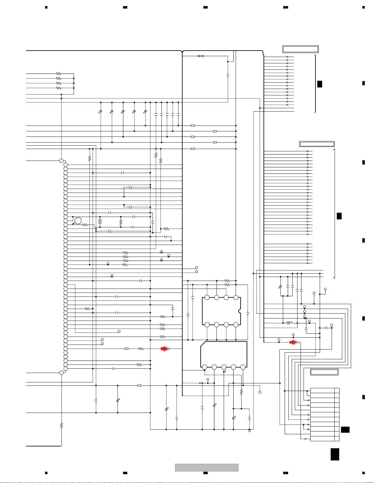
3.4 DVD PCB ASSY(2/4)
A
B
C
D
E
A 2/4
DVD PCB ASSY (A2E514X130)
MEMORY BLOCK
FROM/TO MPEG/MICON/DSP
SD_A0
SD_A1
SD_A2
SD_A3
SD_A4
SD_A5
SD_A6
SD_A7
SD_A8
SD_A9
SD_A10
SD_A11
SD_D0
SD_D1
SD_D2
SD_D3
SD_D4
SD_D5
SD_D6
SD_D7
SD_D8
SD_D9
SD_D10
SD_D11
SD_D12
SD_D13
SD_D14
SD_D15
RAMCS0#
RAMCS1#
RAMRAS#
RAMCAS#
SD_BA0
RAMDQM
RAMWE#
RAMCLK
HA0
1/4A
HA1
HA2
HA3
HA4
HA5
HA6
HA7
HA8
HA9
HA10
HA11
HA12
HA13
HA14
HA15
HA16
HA17
HA18
HA19
HA20
HD0
HD1
HD2
HD3
HD4
HD5
HD6
HD7
HD8
HD9
HD10
HD11
HD12
HD13
HD14
HD15
MEMCS0
RD
WR
P.CON+3.3V
B4007
FCM2012H-102T04
B4008
FCM2012H-102T04
FLASH IC 8M
IC4007 SST39VF800A-70-4C-EK-D
HA16 HA15
C4064
0.1 F
HD15 HA12
HD7 HA11
HD14 HA10
HD6 HA9
HD13 HA8
HD5 HA19
HD12 HA20
HD4 WR
C4062
0.1 F
HD11
HD3
HD10 HA19
HD2 HA18
HD9 HA17
HD1 HA7
HD8 HA6
HD0 HA5
RD HA4
W854
MEMCS0 HA2
STANDARD
HA0 HA1
1.2
A16
3.3
VCCQ
0
VSS
0.7
DQ15
1.9
DQ7
1.3
DQ14
1.2
DQ6
0.6
DQ13
0.7
DQ5
40 41 42 43 44 45 46 47 48
0.8
DQ12
DQ4
3.3
VDD
1.6
DQ11
1.6
DQ3
1.3
DQ10
1.2
DQ2
1.4
DQ9
1.4
DQ1
0.9
DQ8
30 31 32 33 34 35 36 37 38 39
1.6
DQ0
2.6
DE#
0
VSS
2.6
CE#
2.5 1.6
A0
25 26 27 28 29
4.7K
R4040
A15
A14
A13
A12
A11
A10
A9
A8
A19
A20
WE#
RP#
VPP
WP#
A19
A18
A17
A7
A6
A5
A4
A3
A2
A1
1.7
110111213141516171819 22021222324
1.0
0.8
3
1.5
4
2.5
56789
1.3
1.6
1.5
0
0
3.31.6
0
0.1
0.1
R4041
0
1.6
0.7
1.4
1.6
1.6
1.3
1.7
2.5
4.7K
HA14
HA13
RESET
C4039
0.1 F
HA3
F
30
FROM/TO AUDIO/VIDEO
RESET
A
4/4
A 2/4
2206.3V KA
C4063_1
GND
C4095
0.01 B
C4099
0.01 B
DV-PT100-S
1234
Page 31

5678
A
64M SDRAM IC
IC4005 HY57V161610ETP-7
0
VSS
R4048
47K
1.2
1.5
2.0
3.3
0.4
0.5
1.7
0.8
3.3
2.1
1.5
3.3
0.2
0.2
1.0
1.0
1.0
0.9
NC
NC
DQ15
0
VSSQ
DQ14
DQ13
50 51 52 53 54
VDDQ
DQ12
DQ11
0
VSSQ
DQ10
DQ9
VDDQ
DQ8
0
VSS
0
NC
40 41 42 43 44 45 46 47 48 49
0
UDQM
CLK
CKE
0
NC
36 37 38 39
0
A11
A9
A8
A7
A6
A5
30 31 32 33 34 35
A4
0
VSS
28 29
A10/AP
SD_D15 SD_D0
SD_D14 SD_D1
SD_D13 SD_D2
C4040
0.1 F
SD_D12 SD_D3
SD_D11 SD_D4
SD_D10 SD_D5
SD_D9 SD_D6
C4041
0.1 F
SD_D8 SD_D7
RAMDQM RAMWE#
RAMCLK RAMCAS#
2
SD_A11 SD_BA0
SD_A9 RAMCS0#
SD_A8 SD_A10
SD_A7 SD_A0
SD_A6 SD_A1
SD_A5 SD_A2
SD_A4 SD_A3
VDD
DQ0
VDDQ
DQ1
DQ2
VSSQ
DQ3
DQ4
VDDQ
DQ5
DQ6
VSSQ
DQ7
VDD
LDQM
WE
CAS
RAS
CS
BA0
BA1
A0
A1
A2
A3
VDD
3.3
110111213141516171819 22021222324252627
1.5
C4050
3.3
3
0.1 F
0.8
4
0.4
5
0
6789
0.5
0.9
C4045
3.3
0.1 F
1.3
0.8
0
1.3
C4046
3.3
0.1 F
0
3.2
3.2
0.2
3.1
0.5
3.1
1.9
0.2
0
0
0.3
3.3
RAMDQM
RAMRAS#
RAMCS1#
C4047
0.1 F
B
C
D
2206.3V KA
C4021_1
DV-PT100-S
56
E
F
A 2/4
31
7
8
Page 32

1234
3.5 DVD PCB ASSY(3/4)
A
B
C
D
E
F
A 3/4
DVD PCB ASSY (A2E514X130)
RF AMP/DSP BLOCK
DM3
FROM/TO LODER
CP2601
09-5000-024-001-001
1
T-
2
T+
3
F-
4
F+
5
MON(DVD)
6
NC(SW)
7
VOL(DVD)
8
GND(DVD)
9
LD(DVD)
10
LD(CD)
11
VOL(CD)
12
GND(CD)
13
MON(COM)
14
DVD/CD
15
RF
16
C
17
B
OPTICAL PICKUP
18
A
19
D
20
F
21
E
22
VCC
23
VREF
24
GND(PDIC)
CP2602
00_6232_005_006_800
5
LD-
4
LD+
3
OPEN
2
GND(D)
CD2302
1
CLOSE
E
CP2603
00_6232_006_006_800
6
SW(GND)
5
LIMIT SW
4
SLD-
3
SLD+
CD2301
2
SP1-
1
SP1+
D
NC
R2650
R2635
C2634
0.1 F
C2648
0.1 F
4.7K
R2651
4.7K
TP2601
R2649
100
MOT_SLED-
MOT_SLED+
MOT_SPDLMOT_SPDL+
4.7K
HOME
TRTR+
FOFO+
DVDPD
VR_DVD
JG056
DVDLD
CDLD
VR_CD
GND
CDPD
OPU_RF
OPU_C
OPU_B
OPU_A
OPU_D
OPU_F
OPU_E
OPU_VREF
JG052JG063
MOT_LD- OPU_A
MOT_LD+
R2653
TOUT_SW
100
R2652
TIN_SW
100
JG054
JG053
P.CON+3.3V
C2658
100P CH
C2660
C2657
100P CH
C2659
FNP
FNP
C2629
DIP
MIRR
MIRR
0.001 B
C2611
FNP
MP
C2610
FNN
FNN
33 LINK
MB
0.0068 B
0.033 B
C2612
0.1 F
SDEN48
4
C2613
VNA
MLPF
220P CH
C2632
C2633
MEV
MIN
R2648
13K
0.1 F
0.001 B
R2614
00002.33.53.52.62.45.14.34.33.13.101.5
4955051525354555657585966061626364
RX
SDATA
SCLK
V33
LCP
LCN
MNTR
CE
FE
TE
PI
V25
V125
TPH
DFT
MEVO
C2614
+-1%
12K
R2602
1.8M
0.1 B
40 41 42 43 44 45 46 47 48
33 34 35 36 37 38 39
0
1.5
3.3
3.3
4.2
4.1
0
1.8
NC
1.7
1.8
1.6
3.3
1.7
0
3.3
0
R2603
13K +-1%
OPU_E
3.9
3.9
R2624
TP4
RFSIN
CD_E
TP34
C2609
C2640_1
6.3V
VR_SEL
4.7K
TP6
ATON
ATOP
1 DVDRFP
16 CD_A
VPB
VC
TP29
0.1 F
OPU_VREF
JG022
R2615
10
R2616
1K
1006.3V KA
C2641_1
100
KA
R2617
1K
R2618
10
0.1 F
C2626
JG061
JG062
C2624
0.001 B
C2625 0.001 B
VPA
AIP
AIN
IC2601
ZR36708TQC
READ CHANNEL IC
DVDLD
DVDPD
CDLD
TP30
TP31
DVDPD
TP40
TP42
RFAC
RFAC
CDPD
CDPD
C2627
R2601
4.7K
TP25
JG023 JG024
0.033 B
C2628
DIN
BYP
LDON
VNB
TP37
LDON
FNN
0.001 B
TP36
100
R2621
R2620
G
0.7 0.5
4.7K
D
Q2604
S
2SK3018
0
VR_CD
G
VR SEL CTL
0.001 B
P.CON+5V
100
00
Q2605
2SK3018
C2635
R2647
4.7K
R2622
D
S
0
4.7K
G
TP10
R2623
0.7
4.7K
JG021
VR DVD CTL
Q2603
2SK3018
OPU_RF
VR_DVD
R2619
0
D
S
0
VR CD CTL
JG055
3
TP5
0
110111213141516
NC
RFDC
0
DVDRFN
NC
0.0022 B
0.0022 B
0.0022 B
0.0022 B
33P CH
TP19
TP20
TP21
TP22
C2638
C2639
2.5
A2
0
4
B2
2.5
C2
2.5
D2
3.7
789
CP
3.7
CN
2.7
D
2.7
C
2.7
B
2.6
A
2.7
CD_D
2.7
CD_C
2.7
CD_B
2.6
CD_F
17 18 19220 21 22 23 24 25 26 27 28 29330 31 32
2.6 02.6 5.1 5.1 3 .7 5.1 0 .2 0.2 0 3.3 2.7 2.2 2 .3 2.9 0 .2
TP27
TP28
OPU_F
JG019
DVD LD CTL
4.5
Q2601
2SA1036K
1.0
D2601
KDS120RTK
0.1 F
3
2
1
0.1 F
1.0
CD LD CTL
Q2602
4.5
2SA2048
JG020
C2603
C2604
C2605
C2606
C2607
OPU_D
OPU_C
OPU_B
100P CH
100P CH
DVDLD
CDLD
476.3V KA
C2608_1
FCM2012H-102T04
0.1 F
C2636
0.1 F
C2637
FCM2012H-102T04
B2601
B2602
GND
A 3/4
32
DV-PT100-S
1234
Page 33

5678
C2616
470P CH
R2608
1.2K
10K
C2617
0.1 B
R2645
R2643
1K
R2607
1.2K
R2609
1.2K
R2605
+-1%
1K
R2604
C2615 0.1 F
27K +-1%
R2611
4.7K
R2612
4.7K
R2613
4.7K
R2644
R2610
5.1K
0.1 B
0.01 B
C2654
0.01 B
2.2K
C2619
560P CH
C2620
0.0056 B
C2621
0.0056 B
C2622
0.0056 B
C2623
0.1 F
+-1%
C2618
R2646
2.2K
C2655
GND
TP15
TP16
TP17
TP18
TP26
TP38
TP35
TP33
RFA_SDEN
RFA_DATA
RFA_SCLK
AAF_CE
AAF_FE
AAF_TE
AAF_PI
VBIASS0
VBIASS1
DEFECT
LINK
RF
GND
GND
RF_A5V
MOT_SPDL+
MOT_SPDL-
KA
476.3V
C2646_1
C2647
0.1 F
47
6.3V KA
REG-IN
VD2+
TP55
F
C2306 0.1
C2644_1
VIN+OP
VD2-
TP66
KA
C2314_1 10010V
47
6.3V KA
R2306
5.6K
R2316
R2339
VIN-OP
VD1-
R2323
C2642
0.1 F
C2643_1
+-1%
+-1%
R2310
R2312
R2320
R2322
4.7K
4.7K
10K
R2308
1K
TP46
R2338
12K
C2313
0.1 B
R2301
04.02.6 2.6 1.5 1.5 1.5 1.5
S-GND
VCONT
MUTE1
VCC2
REV
FWD
1101112131415161718
C2301
0.1 F
C2302 0.1 B
R2303 2.2
C2303 0.1 B
R2304 2.2
5.6K
5.6K
R2314
+-1%
+-1%
5.6K
5.6K
R2313
R2335
1.5K
R2309
27K
R2305
VIN4-
VIN4
OEC0147A
VD4+
VLD+
TP64
470 +-1%
27K
HS76
NC NC00NC
VREF-IN
IC2301
VD4-
TP65
TP69
HS2301
VREF-OUT
VD3+
4.1
763WSA0026
REG-OUT
MOTOR DRIVE IC
VD3-
TP68
R2307
TP138
MUTE234
VLD-
456789
C2304
220P CH
R2315
10K
R2317
22K
1.0 2.5 0 1.5 1.7
38
272829330313233343536
37
TP56
B2605
FCM2012H-102T04
0.1 F
C2645
B2604
FCM2012H-102T04
B2603
FCM2012H-102T04
5.6K
R2318
220P CH
C2305
C2309
TP45TP139
27K
1.5K
R2319
27K
R2321
R2326
1M
1.5 1.5 1.54.2
VIN3VCC1
VIN3-
VO_OP
VCCS
VD1+
C2310_1 10010V KA
C2307 0.1 B
C2308 0.1 B
1.2
1.2
R2329
0.001 B
R2334
R2324
3.9K
TP140
VIN2
VIN1+A
10K
1K
R2327
19220212223242526
VIN2-
VIN1-A
1.51.51.58.88.84.14.03.05.104.14.14.10.90.88.800
R2328
4.7K
JG057
JG058
VIN 1 VIN2+
R2325
C2312
4.7K
3.3K
C2311
0.001 B
R2337
R2330
TP141
0.1 B
10K
1K
TP24
R2331
FROM/TO MPEG/MICON/DSP
R2336
470 +-1%
4.7K
TP1
TP2
TOUT_SW
TIN_SW
RFA_SDEN
RFA_DATA
RFA_SCLK
AAF_CE
AAF_FE
AAF_TE
AAF_PI
VR_SEL
FNN
FNP
VBIASS0
VBIASS1
DEFECT
LINK
MIRR
LDON
HOME
GND
GND
P.CON+5V
P.CON+A5V
P.CON+3.3V
SMUTE
TRACK_DAC
FOCUS_DAC
SPINDLE_PWM
SLED_PWM
ADCIN_7
ADCIN_5
ADCIN_6
VCC+9V
M_GND
SPDL_SENS
TRAY_CLOSE
TRAY_OPEN
A
1/4A
B
C
D
E
MOT_LD-
NOTE:THE DC VOLTAGE EACH PART WAS
MEASURED WITH THE DIGITAL TESTER
DURING PLAYBACK.
MOT_LD+
TR+
TR-
FO+
FO-
MOT_SPDL+
MOT_SPDL-
MOT_SLED-
MOT_SLED+
DV-PT100-S
56
F
A 3/4
33
7
8
Page 34

1234
3.6 DVD PCB ASSY(4/4)
A
B
C
A 4/4
DVD PCB ASSY (A2E514X130)
AUDIO/VIDEO BLOCK
FROM/TO MPEG/MICON/DSP
DAC_VIDEO_A
DAC_VIDEO_C
DAC_VIDEO_B
DAC_VIDEO_D
P.CON+5V
RESET
MC
MD
ML
1/4A
AMCLK
ABCLK
ALRCLK
ASDATA0
V_SW
DVD-H
SYS_MUTE
GND
GND
DAC_VIDEO_A
C8124
DAC_VIDEO_C
C8104
DAC_VIDEO_B
C8107
DAC_VIDEO_D
150P CH
150P CH
150P CH
C8110
100P CH
C8115
12P CH
L8105
1uH
0305
C8105
12P CH
L8102
1uH
0305
C8108
12P CH
L8103
1uH
0305
C8111
12P CH
L8104
1uH
0305
C8127
C8106
C8109
C8112
W815
150P CH
W818
150P CH
W819
150P CH
W820
33P CH
FROM/TO MEMORY
C8120
RESET
A
2/4
B8103
FCM2012H-102T04
0.1 F
D
2.4
IC8102
PCM1753DBQR
STEREO DAC IC
E
9
0
1006.3V KA
C8119_1
NC
0
5678
VCC
VDD
ZEROL/NA
ZEROR/ZEROA
12 13 14 15 16
3.3 0 0 0 3.3 1.7
NC
1025V KA
ZERO
AGND VOUTR
2.4
C8121_1
VOUTL
VCOM
10 11
DGND
MD
MD
LRCK
MC
MC
234
ML
1.61.11.63.34.92.5
DATA
ML
C8114
1B
C8125
1B
C8113
1B
C8126
1B
1
BCK
SCK
AMCLK
ABCLK
ASDATA0
ALRCLK
R8113
470
R8112
470
6
7
F
34
A 4/4
PLAYBACK COLOR SIGNAL
PLAYBACK LUMINANCE SIGNAL
COMPONENT SIGNAL(U)
COMPONENT SIGNAL(V)
AUDIO SIGNAL(PB)PLAYBACK VIDEO SIGNAL
DV-PT100-S
1234
Page 35

5678
A
5
DAC_A_VIDEO
10
12 3 4
DAC_C_VIDEO
A
B
C
9
8
DAC_B_VIDEO
DAC_D_DVD_VIDEO
D
DVD-H
V_SW
DAC_A_VIDEO
RESET
D8111 MCL4148
ZERO
R_AUDIO
L_AUDIO
DAC_B_VIDEO
DAC_C_VIDEO
DAC_D_DVD_VIDEO
SYS_MUTE
Y
V
U
C
D8112
MCL4148
G
R
B
CVBS
R8101
C8122
CVBS
Y
C
Y
V
U
CVBS CVBS
1K
JG030
JG033
JG031
JG036
JG034
W824
JG035
JG048
JG042
JG040
JG038
0.001 B
JG013
W826
JG037
FROM/TO TUNER/JACK
CP8101_2
IMSA-9604S-14F
V SW
14
13
Y(G)
12
DVD-H
DVD RESET
AUDIO-R
AUDIO-L
ZERO
GND
GND
V(R)
GND
U(B)
GND
CVBS
11
10
9
8
7
6
5
4
3
2
1
B
C
D
CP8001
B 3/6
E
NOTE:THE DC VOLTAGE EACH PART WAS
MEASURED WITH THE DIGITAL TESTER
DURING PLAYBACK.
DV-PT100-S
56
F
A 4/4
35
7
8
Page 36

1234
3.7 VCR PCB ASSY(1/6)
B 1/6
A
B
FROM/TO HI-FI/DEMODULATOR
TO_NORMAL_A
FROM_NORMAL_A
C
CYLINDER UNIT
D
HEAD AUDIO
E
F
CONTROL ASSY
HEAD ASSY
FULL ERASE
VCR PCB ASSY (A2E514X010)
Y/C/AUDIO/CCD/HEAD AMP BLOCK
FROM/TO POWER
P.CON+5V
B
6/6
5/6B
FROM/TO CYL
CP101
TOC-C09X-A1
9
8
7
6
5
4
3
2
1
FROM/TO HEAD AUDIO CONTROL
CP102-1
IMSA-9604S-04C
4
3
2
1
2F041508
TO FULL ERASE HEAD
CP103
B2013H02-2P
2
1
FSC
HF1
HF_COM
HF2
HF1 (R)
HF_COM
HF2 (L)
SP-CH1 (R)
SP_COM
SP-CH2 (L)
EP/LP-CH1 (R)
EP/LP COM
EP/LP-CH2 (L)
AUDIO REC
AUDIO PB
CTL+
CTL-
FFC
CD102
FE HEAD(GND)
FE HEAD(HOT)
GND
15P CH
AUDIO PB SW
KTC3875S_Y_RTK
AUDIO PB SW
KTC3875S_Y_RTK
GND
HOT
CTL+
CTL-
C140
Q102
Q101
P.CON+5V
C158
P.CON+5V
TO_NORMAL_A
P.CON+5V
R140
V.REC_ST-H
R101
560
W819
0
0.7
0
0
0.7
0
W862
W805
1B
W852
C174 476.3V
2.2K 1/4W
R102
10K
R103
10K
W863
R105
1K 1/4W
5.2
0
5.3
C129
1B
KA
SW
Q103
DTA124EKA
5
C101_1
0.033100V
MMTS
6
5
680
R106
COIL,BIAS OSC
L101
1626010
1
2
34
2206.3V KA
C104
IC101
LA71206M-MPB
Y/C/AUDIO/CCD/HEAD AMP IC
C166
0.068 B
C169
0.047 F
C165
0.047 F
1B
C162
C105
C106
C107
2216V KA
C108
0.01 B
0.015 B
0.01 B
R107
3.9K
0
L102
100uH
0305
0
BIAS OSC
0
Q104
KTC3203_Y
C109
0.1 B
0
BIAS CTL
Q105
KTA1266
5.2
R142
5.2
R108
22K
C110_1
4716V YK
COMP
ENV.DET
H.AMP_SW
R136
22K
R137
C154
0.1 B
OUT
COMP
AUDIO
2.1
2.9
1.6
1.8
1.9
1.8
5.0
1.8
1K
1.6
1.8
1.8
1.8
2.3
4.9
2.3
2.3
ENV
DET
KILL
616263646566676869
0
70717273747576777879
0
0
0
2.3 2.3 2.3 2.32.3 2 .3 0 2.3 2.3
C112
2206.3V KA
NOTE:THE DC VOLTAGE EACH PART WAS
HA SW
DET
HA
GND
CHROMA
DET
ACC
DET
P
R
P
HA VCC
HA
PRE GND
P
R
P
A-GND
1
2
3
A-VCC
Vref
2.3V
123 4
C116
0.1 F
R109
1K
1/4W
3310V KA
C115_1
C117
0.01 B
0.1 B
C114
MEASURED WITH THE DIGITAL TESTER
DURING PLAYBACK.
C.ROTARY
22K
AUDIO_MUTE-H
R138
R139
12K 1/4W
C156
C-ROT
C-GND
MUTE
RF-SW
IN
H
L
H
L
ALC
ALC
DET
PB,EE
EQ
AMP
SP,LP
8.2K
R110
8.2K
R111
R112
330K
C118
0.01 B
C119
R113
H.SW
5
12K
0.1 F
C120
1025V KA
220
Y/C_CS
C-LPF
+
R
P
REC:LP<EP
PB:EP
Y/C_DATA
SERAIL
DECODER
RP
PB,EE
7
C121
0.0012 B
1B
Y/C_CLK
Main
CONV
4.21M
BPF
Sub
CONV
VREF
8809
0.0027 B
R114
20K
C122
4.95.25.25.205.204.84.8
5253545556575859660
C-VCC
LPF
REC
AMP
R115
820
B 1/6
36
DV-PT100-S
1234
Page 37

5678
A
P.CON+5V
W817
C152
1B
C151
R133
8.2K
KTC3875S_Y_RTK
4.9
R129
3.9
1.8K
3.3
4716V KA
1B
C146
C145
0.022 B
2
R131
1.5K
BUFFER
Q109
3.3K
R132
C147
0.022 B
C148
P.CON+5V
W815
1B
C142_1
R127
680K
4716V KA
C143
1B
X101
3.579545MHz
3.579545MHz
4.8
320FH
VX01
PB
REC
APC
APC
BEFORE
P
R
AFTER
BGA
R
P
3.58M
BPF2
B-UP
AMP
ACC
AMP
RPPP
ACC
DET
P
R
DETAIL
CLAMP
ENH
NL
NL
EMPHA
EMPHA
FM
MOD
R-EQ
NORMAL
TEST
LINE
REC
AMP
FM-EQ
FM
R
P
AGC
MUTE
PHASE
PHASE
AUTO
EQ
BIAS
fo-ADJ
10 1 1 1 2 13 14 15 16 17 18 19 20
4.80.8 1.1 1.1 1.4 02.0 0.22.62.6
15K
R116
4.750V KA
C123
R117
VCO
P
FM EQ
EQ
Q-ADJ
R
REC
AFC
BGA
BGA
R
Y-LPF
DOUBBLE
LIM
PB
VHS
6.8K
SLD
PB-C
S-EQ
P
R
SOPB
NC
B
CNC
PB
AMP
B.D
P
3.58M
BPF1
YNR/COMB
N.L.
DEEM
NC1
FM
DEM
P
FM
AGC
FIL
C124
ALWAYS
5V
R
Y-GND
1B
R
PB-C
SUB
LPF
MAIN
DE-EM
Y/C
MIX
P
VDD 4Fsc
R
PLL
TIMMING OUT
AUTO-BIAS
DRIVER
CLAMP
CCD
CLAMP
VIDEO
AGC
1/2
FBC
R
P
R
P
QV/QH
SYNC
SEP
V.SYNC
SEP
4.7K
MAIN
S
EMPHA
DET
FIL
C125
390P CH
C126
VCA
1
2
3
6DB
FSC
C144
0.01 B
FROM/TO TUNER/JACK
DVD_V_OUT[DAC_D]
FRONT_V_IN
TU/REAR_V_IN
Y/C_VIDEO_OUT
C141
BUFFER
Q107
KTA1504S_Y_RTK
1B
C134
1B
C135
0.2250V YK
C136
2235V YK
C132
1006.3V KA
C131_1
R126
1.6
1B
1.8K
2.20
C137
C102
1B
C139
0.1 B
1025V KA
W801
R123
R124
82K
W828
2.2K 1/4W
C138
150V YK
W809
R122
100K
R143
1K
TU/REAR_V_IN
FRONT_V_IN
R141
DVD_V_OUT[DAC_D]
1K
1
Y/C_VIDEO_OUT
DUMMY_V.SYNC
P.CON+5V
4FSC
C.SYNC
0.01 B
0.82.21.24.94.93.22.1 4.1 3.3 3.2
4142434445464748495051
CLOCK
0
VSS
1.6
OUT
0
VSS
3.2
IN
C133
2.5
VCA
3.2
3.3
2.6
VCP
2.6
4.1
REG
4V
2.3
BAL
2.3
TC1
2.1
AGC
1.6
TC2
3.6
4.1
5.0
4.4
Y-VCC
3.2
2.1
B
21 22 23 24 25 26 27 28 29 30 31 32 33 34 35 36 37 38 39 40
2.8NC
FSC
FROM/TO SYSCON
4FSC
Y/C_CLK
Y/C_DATA
Y/C_CS
DUMMY_V.SYNC
V.REC_ST-H
C.ROTARY
AUDIO_MUTE-H
CTLCTL+
H.AMP_SW
COMP
ENV.DET
H.SW
C.SYNC
3/6B
B
C
2/6B
D
R144
220K1/4W
1.8K
R119
E
0.1 B
4
FROM_NORMAL_A
C127
180P CH
V.ENV
TP101
NC
3
PLAYBACK VIDEO SIGNAL
RECORD COLOR SIGNAL
RECORD LUMINANCE SIGNAL
CAUTION: DIGITAL TRANSISTOR
AUDIO SIGNAL(REC)
AUDIO SIGNAL(PB)
PLAYBACK COLOR SIGNAL
PLAYBACK LUMINANCE SIGNAL
TUNER VIDEO SIGNAL
DV-PT100-S
56
F
B 1/6
37
7
8
Page 38

1234
3.8 VCR PCB ASSY(2/6)
VCR PCB ASSY (A2E514X010)
FROM/TO POWER
A
B 2/6
6/6B
DVD_POWER_CTL
AT+12.6_V
P.CON+5V
AT+5V[M-CON]
VCR_POWER_ON-L
POWER_FAIL
AT+5.2V
B
C
D
E
MOTOR_GND
FROM/TO DECK
CP3001
TMC-J12P-B2
1
CAP FG
2
CAP VCO
3
VCC
4
CAP.M/F/R
5
I LIMIT
6
MOTOR GND
7
GND
8
LD/CY VCO
9
CAP CTL
10
LDM CTL
11
CYL FG/PG
12
CYL CTL
CAPSTAN DD UNIT
BOT SENSOR
Q3008
ST-304L
5.0
0
R3004
SYSCON BLOCK
TX
RX
GND
10K
R3035
C3033
22016V YK
L3002
22uH
9C08A
5.0
D3001
0
LTE-3271T-012A-O
R3016
330K
270 1/4W
TAB SW
R3026
SW3001
LSA-1144EAU
R3003
3.3K
C3040
EOT SENSOR
Q3006
ST-304L
270K
CAP_LIMIT
CAP_FG
AT+12.6_V RF_CH_SW
P.CON+5V
CAP_F/R
CAP_LIMIT
1F
AT+12.6_V
CONTROL_IN
LDM_CTL H.AMP_SW
CYL_FG/PG
CYL_DRIVE
AT+5.2V
C3005
0.001 B
C3006
0.001 B
EOT
BOT
(LED_GND)
R3011
AT+5.2V
47K 1/4W
TAB_SW
LDM_CTL
CAP_F/R
C3008
0.0047 B
CONTROL_IN
CYL_DRIVE
CYL_FG/PG
R3001
5.6K
C3007 0.1 B
AT+5V[M-CON]
C3066
0.01 B
9
R3008
1K
6
AT+5.2V
6.8K
R3032
10K
C3010
R3015
W835
0.001 B
REC_MUTE_H
C3053
47K 1/4W
R3014 56K
R3012
56K 1/4W
R3017
560
R3020
560
C3020
0.022 B
R3057
22K
TV/VCR
POWER_MUTE-L
SYS_MUTE
SERVICE
NC SERVICE
TP3001
AV_SW1
Y/C_CS
AUDIO_MUTE-H
V.REC_ST-H
C.ROTARY
COMP
R3031
1M
H.SW
HIFI_H.SW
C3004 0.022 B
DUMMY_V.SYNC
C.SYNC
CTL+
R3007
CTL-
8
C3016
2216V KA
C3024
100GT01006
2.53.45.1
VCL
MD0
85
86
VCR_H
87
POWER MUTE-L
C SYNC
111
VCC (BACK UP)
112
CTL(+)
CTL(-)
476.3V KA
C3015
820P CH
C3025
15P CH
X3001
12P CH
10MHz
R3034
OSC2
CTL BIAS
R3022
C3018
C3019
R3027
1M
VSS (GND)
CTL FB
67
MD0
0.1 B
C3009
AT+5V[M-CON]
W836
10K
R3033
0.1 B
3.3
5.0
NC
8586878889
0
CAP LIMIT
5.0
5.1
NC
0
5.0
5.0
0.1
5.1
0
0
2.4
0
2.5
2.7
3.0
2.5
2.5
2.7
2.7
0.4
5.1
REC MUTE-H
SYS MUTE
90919293949596979899
AV SW2
AV SW1
Y/C CS
RF CH SW
AUDIO MUTE-H
V.REC ST-H
LDM_CTL
CAP FWD-L
C.ROTARY
0
H.AMP SW
100
0
COMP
CAP FULL
0
CYL SPEED UP
D FG/PG
VIDEO H.SW
HIFI H.SW
DRUM PWM
CAP PWM
0
DUMMY_V.SYNC
0
VSS (GND)
110 101102103104105106107108109112 111
SVSS (GND)
CTL REF
002.5 0 2.5 0 .1 2.6 2.5 2.3 5 .1 2.0 2 .0
C3013
2216V KA
C3052
OSC1
CTL AMP(O)
150K
7
150P CH
0.1 B
15K
C3041 0.0015 B
10
RESET
C3050 0.01 B
R3062 1K
757677787988081828384
X1
/RESET
CTL SMT(I)
CAP FG
9
1K
R3056
CAP_FG
FWE
SEG_10
R3037 47K
NC
00
01.51.45.100
7374
X2
FWE
SEG10
AFC OSC
AFC PC
SVCC (P.CON5V)
111012213 4 5
R3025
470
L3003
12uH
C3044
12P CH
CH
1B
470P
C3022
C3001
F
38
B 2/6
C3027
CAUTION: DIGITAL TRANSISTOR
CAUTION: DIGITAL TRANSISTOR
P.CON+5V
AT+5.2V
MS_SEN B
Q3004
RPI-352C40N
5.1
23
1
0.9
R3083
4
33K
5.1
1.3
MS_SEN-B
MS_SEN A
Q3005
RPI-352C40N
0.4
R3050
5.10.9
23
1
4
1.3
33K
100 1/4W
R3087
MS_SEN-A
REEL SENS
Q3002 RPI-303
120
R3002
1.2
2
1
34
5.2
1/4W
2.4
0
11
REC_L/REEL-T
47K
R3006
W811
KA
476.3V
0.1 F
C3029
DV-PT100-S
1234
Page 39

5678
SCL
1/4W
SEG5
SI1/RX
SO1/TX
VCC (BACK UP)
SEG1
Y/C DATA
SDA
W839
W840
4.84.8
IIC CLK
IIC SDA
4G/TIME SHIFT LED
SEG_2
SEG_3
SEG_4
4.84.804.80
SEG4
SEG3
Y/C CLK
5G/CS/BS LED
3G/TV/VCR LED
2G/DUB/REC LED
1G/VCR/T-REC_LED
VCR LED
DVD LED
DVD_POWER_CTL
DVD RESET
NC
0
JUST_CLK
SEG_9
SEG9
SEG_8
SEG_7
SEG_6TXSEG_5
R3028 47K
NCNC
000
4.8
0
SEG6
SEG7
SEG8
56
55
54
IC3001
OEC0147A
SYSCON/TIMER/SERVO IC
31
ST SELECT
KEY-A
30
KEY-B
29
CV IN2
CV IN1
C3038
1F
R3043
OVCC
0.1 F
C3065
470K
AT+5V[M-CON]
V CYNC
AFC LPF
C SYNC/H SYNC
13 14 15 16 17 18 19 20 21 22 23 24 25 26 27 28
1.5 0 .4 0 3 .1 2.6 5 .1 2.6 0 0 2.5 0 2.6 0 0 1.3 1.3
5.6K
KA
R3030
2.2
50V
C3032
SW_V_OUT
CV OUT
OVSS(GND)
NC
VIDEO_OUT
4FSCOUT/2FSCOUT
4FSCIN/2FSCIN
C3017
0.001 B
4FSC
SYNC DET/
V ENV
AVSS (GND)
BOT
ENV.DET
REC_L/
POWER ON-L
VIDEO_MUTE-H
REC_L/
REEL T
VSC_L/ REEL S
POWER FAIL
AVCC (BACK UP)
TAB SW
AFT S.CURVE
HiFi ENV
ST SELECT
BOT-H
EOT-H
MS_SEN-B
EOT
R3044 3.3K
C3061
05.04.9
57585960616263646566676869707172
SEG2
VSS (GND)
REM IN
REEL T
PG
MS SEN-A
MS SEN-B
MS_SEN-A
R3045 3.3K
0.1 F
5.1
51 52 53 54 55 56
0
0.1
5.0
5.1
0
0
2.5
3.7
0
5.2
5.2
29 30 31 32 33 34 35 36 37 38 39 40 41 42 43 44 45 46 47 48 49 50
D3007
1SS133
R3010
10K
AT+5V[M-CON]
0
4.8
5.0
5.0
5.0
5.0
5.0
5.0
0.3
5.1
3.3
4.7
5.0
W867
0
0
NC
C3031
0.0015 B
RX DRIVE
Q3003
DTA124EKA
W838
R3055 22K
R3038 4.7K
R3021 1K
C3014
180P CH
1F
C3034
1K
R3063
R3053
SW_V_OUT
AT+5.2V
5.2
5.3
4.7K
R3009
C3036 0.1 F
R3036
100P CH
C3049
470K
0
W837
10K
0
0
3.4
RX
RX DRIVE
Q3007
DTC124EKA
SEG_1
Y/C_DATA
Y/C_CLK
5G/CS/BS_LED
4G/VSC_LED
3G/TV/VCR_LED
2G/DUB/REC_LED
1G/VCR/T-REC_LED
VCR_LED
DVD_LED
DVD_POWER_CTL
DVD_POWER_CTL
REM_IN
REC_L/REEL-T
VCR_POWER_ON-L
VIDEO_MUTE-H
AT+5.2V
C.SYNC
1SS133
D3002
POWER_FAIL
AT+5V[M-CON]
TAB_SW
AFT-S.CURVE
HIFI_ENV.DET
ST_SELECT
KEY-A
KEY-B
10K
R3046
10K
R3047
AT+5.2V
TP3002 H.SW
H.SW
JG3002 JG3003 JG3004 JG3005 JG3007 JG3008JG3006
NC
FROM/TO Y/C/AUDIO/CCD/H.AMP
DUMMY_V.SYNC
C.SYNC
V.REC_ST-H
C.ROTARY
AUDIO_MUTE-H
CTLCTL+
H.AMP_SW
COMP
ENV.DET
H.SW
Y/C_CS
Y/C_DATA
Y/C_CLK
4FSC
FROM/TO TUNER/JACK
FROM/TO HI-FI/DEMODULATOR
REC_MUTE_H
HIFI_ENV.DET
HIFI_H.SW
AUDIO_MUTE-H
SCL
SDA
ST_SELECT
FROM/TO OPERATION1/DISPLAY
DVD_LED
VCR_LED
KEY-A
KEY-B
REM_IN
1G/VCR/T-REC_LED
2G/DUB/REC_LED
3G/TV/VCR_LED
4G/VSC_LED
5G/CS/BS_LED
SEG_1
SEG_2
SEG_3
SEG_4
SEG_5
SEG_6
SEG_7
SEG_8
SEG_9
SEG_10
DVD_POWER_CTL
RF_CH_SW
SW_V_OUT
AV_SW1
SCL
SDA
AFT-S.CURVE
TV/VCR
VIDEO_OUT
POWER_MUTE-L
VIDEO_MUTE-H
DVD_RESET
SYS_MUTE
A
1/6B
B
3/6B
C
B
5/6
D
4/6B
E
IC3003
PST3231NR
SYSTEM RESET IC
NC
OUT IN GND
123
KA
0.4750V
C3045
NOTE:THE DC VOLTAGE EACH PART WAS
RESET
R3049
NC
00
47K
45
NCNC
05.05.0
D3009
1SS133
MEASURED WITH THE DIGITAL TESTER
DURING PLAYBACK.
R3051
C3021
C3002
18K
1025V KA
1B
AT+5V[M-CON]
C3023
56
SCL
SDA
5.2
05.04.9
TEST
A1
00
5678
SDA
SCL
VSS
A2
00
4706.3V YK
VCC
A0
1 234
IC3099_1
S-24C02BFJ-TB
C3030
1F
AT+5.2V
TX
MD0
RESET
FWE
AT+5V[M-CON]
RECORD LUMINANCE SIGNAL
RECORD COLOR SIGNAL
PLAYBACK LUMINANCE SIGNAL
PLAYBACK COLOR SIGNAL
F
EEP ROM IC
B 2/6
DV-PT100-S
7
8
39
Page 40

1234
3.9 VCR PCB ASSY(3/6)
A
B
C
D
B 3/6
TU301
115-V-H035ARE
18
19
1
A.IN
2
CH
3
+B
4
CONTROL
5
V.IN
7
FSC
8
NC
9
10
CLOCK
11
DATA
12
AFT
A.OUT
13
14
SIF OUT
TU 32V
15
16
NC
V.OUT
17
20
21
VCR PCB ASSY (A2E514X010)
TUNER/JACK BLOCK
1K1/4W
Q301
33K
1K
C317
100P CH
R305
0
00
C318
RF_CONV_A_OUT
1025V KA
R302
1K
R306
W879
AFT-S.CURVE
C313
1025V KA
RF_CH_SW
P.CON+5V
TV/VCR
FSC
22
SCL
SDA
SIF_OUT
+32V
TU_V_OUT
C8005
C8014
0.1 F
C8013
1050V KA
P.CON+12V
VIDEO MUTE SW
DTC124EKA
VIDEO_MUTE-H
RF MUTE SW
KTC3875S_Y_RTK
R301
C315
R304
1025V KA
L301
22uH 0305
2206.3V YK
C309
NCNC
NC
NC
NC
C307
33P CH
C302
100P CH
C303
0.1 F
C308
0.01 B
4706.3V YK
Q8003
C8011
0
2206.3V KA
R8009
4701/2W
3.3
0
REAR OUT JACK
MSP-213V1-432_NI_LF
1
2345
R
2206.3V KA
C8015
3.3
2.6
BUFFER
0
Q8004
KTA1266
J8001
L
EE
H1H1 H2
V
R8010
R8011
100 1/4W
C8021
0.1 F
68
C8022
C8023
0.022 B
C8024
4716V YK
R8014
100
KTC3875S_Y_RTK
4716V YK
VCC
GND
B8001
P.CON+5V
R8015
MUTE SW
Q8005
R8002
INPUT
123
OFTG038101
OPTICAL
OS8001
R8054
2.2K
R8003
B8003
FCM2012H-102T04
SPDIF
100
MUTE SW
Q8006
KTC3875S_Y_RTK
0
R8016
0
2.2K
0
3.3K
D AUDIO DRIVER
Q8001
KTC3875S_Y_RTK
0
1.7
1.2
R8006
1.5K
C8025
FCM2012H-102T04
R8007
FCM2012H-102T04
0
R8017
0
2.2K
0
R8005
68
0.1 B
100K
220
B8002
R8032
MUTE SW
Q8007
DTA124EKA
150
5.20
5.0
DVD AUDIO OUT
J8006
MSP-213V1-732_NI_LF
EE
1
2345
H1H1 H2
470
470
R8008
R8004
ZERO
SYS_MUTE
DVD_A_OUT_L
150
R8059
4.7K 1/4W
15
33K1/4W
2.6
R8012
DVD_A_OUT_R
R8056
100P CH
C8028
Q8002
MUTE SW
DTC144EKA
3.2
0
Q8008
KTC3875S_Y_RTK
MUTE SW
0
-0.3
0
E
F
40
CAUTION: DIGITAL TRANSISTOR
CAUTION: DIGITAL TRANSISTOR
PLAYBACK VIDEO SIGNAL
TUNER VIDEO SIGNAL
PLAYBACK LUMINANCE SIGNAL
PLAYBACK COLOR SIGNAL
RECORD COLOR SIGNAL
RECORD LUMINANCE SIGNAL
AUDIO SIGNAL(REC)
AUDIO SIGNAL(PB)
B 3/6
1234
TU/REAR_V_IN
TU_V_OUT
W810
DV-PT100-S
VIDEO
FRONT AV JACK
75
R8019
E
1
2
H
J8003 MSP-281V42-B
E
1
AUDIO L
2
H
FRONT AV JACK
J8004 MSP-281V40-B
AUDIO R
FRONT AV JACK
J8005 MSP-281V31-A
C8099
470P CH
C8004
470P CH
FRONT_A_IN_L
E
1
23
HNC
C8019
1025V KA
FRONT_A_IN_R
FRONT_V_IN
Page 41

5678
A
MSP-213V1-652_NI_LF
C8054
33P CH
C8055
33P CH
D8006
R8027
4.7K
5.0
R8021
-0.2
1K
0
R8022
-0.3
1K
0
MUTE SW
Q8009
KTC3875S_Y_RTK
YUV OUT
J8007
1
2345
AT+5.2V
1SS133
MUTE SW.
Q8010
5.0
DTA143EKA
3.3K
4.750V KA
C8032
EE
H1H1 H2
YVU
P.CON+5V
DVD_V[DAC_B]
D8004
R8023
1SS133
5.0
D8005
0
1SS133
0
MUTE SW.
Q8011
DTC124EKA
MUTE DET
Q8012
KTC3875S_Y_RTK
DVD_V_OUT[DAC_D]
Y/C_VIDEO_OUT
R8024
0.3
0
C8033
220P CH
C8034
4.7K
0.6
VIDEO OUT SW
SW8001
SK42H01G9A
NC
1
34 5 6 78
2
11 12
13 14 15 16 17 18
NC
10K
R8048
C8056
33P CH
DVD_Y_VIDEO[DAC_A]
C8035
13
2206.3V YK
1K
R8025
14
470K
R8026
R8029
10K
R8028
C8031
4.750V KA
C8010
1025V KA
R8049
R8030
470
10K
C8036
2.2
V_SW
KA
2.250V
R8031
470
R8033
2.250V KA
NC
NC
1.5K
C8037
2250V KA
R8034
1.5K
8.4
NC
C8038
0
DVD_U[DAC_C]
R8037
10K
P.CON+12V
56 1/4W
R8036
2250V YK
10016V KA
C8039
R8035
10K
6
SW1
Vin1
5
V OUT
GND
VccVin2
4
IC8005
MM1501XNRE
AV SW IC
C8058
L8001
W854
12K
R8038
C8043
330P
CH
5.8
1234
+
VCC
C8041
R8039
0.1 F
07.8
1
7.0
2
11.7
3
56
10P CH
12
YC
34
Y/C SEPA
MDC-070V-B_LF
C8045
150P CH
5.8 5.8 0
+
-
330P CH
12K
J8008
A_GND
5678
5.85.85.811.6
0.33uH
C8044
12
0.1 F
C8057
C8060
L8002
W849
C8048
330P CH
R8041
10K
IC8001
NJM4580M
AUDIO_AMP IC
R8040
47K
C8047
330P CH
W823
R8042
C8050
10K
150P CH
10P CH
0.33uH
R8043
10K
R8044
R8045
100K
R8046
100K
47K
R8047
10K
3350V YK
C8051
AUDIO_OUT_R
AUDIO_OUT_L
AT+5.2V
VIDEO_OUT
POWER_MUTE-L
AV_SW1
SW_V_OUT
P.CON+9V
V_SW
DVD_Y_VIDEO[DAC_A]
DVD_POWER_CTL
DVD_RESET
ZERO
DVD_V[DAC_B]
C8063 10006.3V YK
DVD_U[DAC_C]
C8062 10006.3V YK
DVD_V_OUT[DAC_D]
C8061
10006.3V YK
FROM/TO AUDIO/VIDEO
C8020
CP8001
IMSA-9604S-14C
100P CH
DVD RESET
C8009
0.0015 B
C8008
0.0015 B
FROM/TO Y/C/AUDIO/CCD/H.AMP
DVD_V_OUT[DAC_D]
FSC
TU/REAR_V_IN
FRONT_V_IN
Y/C_VIDEO_OUT
FROM/TO SYSCON
DVD_POWER_CTL
DVD_RESET
SYS_MUTE
SCL
SDA
AV_SW1
TV/VCR
RF_CH_SW
AFT-S.CURVE
POWER_MUTE-L
VIDEO_MUTE-H
VIDEO_OUT
SW_V_OUT
FROM/TO HI-FI/DEMODULATOR
DVD_A_OUT_R
DVD_A_OUT_L
SIF_OUT
FRONT_A_IN_L
FRONT_A_IN_R
AUDIO_OUT_L
AUDIO_OUT_R
RF_CONV_A_OUT
FROM/TO POWER
GND
+32V
AT+5.2V
P.CON+5V
P.CON+12V
SPDIF
P.CON+9V
V SW
Y(G)
DVD-H
ZERO
AUDIO-R
GND
AUDIO-L
GND
V(R)
GND
U(B)
GND
CVBS
FFC
CD8001
2F0E1001
6/6B
1
2
3
4
5
6
7
8
9
10
11
12
13
14
3/6B
5/6B
CP8101_2
B
A 4/4
C
1/6B
D
E
F
56
DV-PT100-S
B 3/6
41
7
8
Page 42

1234
3.10 VCR PCB ASSY(4/6)
A
B
C
D
B 4/6
VCR PCB ASSY (A2E514X010)
OPERATION/DISPLAY BLOCK
SEG1 SW
Q664
DTC124EKA
0
1.9
2.0
5.2 1.7
1G SW
Q665
KTA1504S_Y_RTK
4.9
DTC124EKA
820
R675
SEG2 SW
Q663
0
4.0
R674
180
0.4
SEG3 SW
Q662
DTC124EKA
4.0
R673
180
0.40
2G SW
Q661
KTA1504S_Y_RTK
1.75.2
SEG4 SW
4.9
Q660
DTC124EKA
4.0
820
R671
R672
180
1.10
V651 CO2D0M3-A
R670
SEG5 SW
Q658
DTC124EKA
01.0
3G SW
Q659
3.0
KTA1504S_Y_RTK
4.9
R669
180
R668
180
1.75.2
SEG6 SW
Q657
DTC124EKA
00.4
820
4.0
R667
180
1101112131415 23456789
R665
180
R666
4G SW
180
Q654
KTA1504S_Y_RTK
1.7
4.9
R664
R662
SEG7 SW
Q656
DTC124EKA
3.1 0
0
5.2
820
180
R663
180
KTA1504S_Y_RTK
SEG8 SW
Q655
DTC124EKA
0
5G SW
Q651
1.3 5.2
4.9
03.5
R661
SEG9 SW
Q653
DTC124EKA
0.4 0
4.0
820
SEG10 SW
Q652
DTC124EKA
0.9 0
4.0
E
F
42
B 4/6
SEG_1
1G/VCR/T-REC_LED
DVD LED
5
CP651
IMSA-9604S-05F
FROM/TO OPERATION1/LED
C
SEG_2
KEY-A
NC
GND
KEY-A
2
3
4
CP681
SEG_3
KEY-B
1
SEG_4
2G/DUB/REC_LED
R683
0
560
SEG_5
DVD_LED
DTA124EKA
5.25.2
3G/TV/VCR_LED
DVD LED SW
Q666
W802
SEG_6
4G/VSC_LED
SEG_7
VCR_LED
R653
D651
VCR_LED
SEG_8
5G/CS/BS_LED
330 1/4W
LTL-1CHEE-002A
SEG_9
SEG_10
DV-PT100-S
1234
Page 43

5678
A
FROM/TO SYSCON
CAUTION: DIGITAL TRANSISTOR
CAUTION: DIGITAL TRANSISTOR
NOTE:THE DC VOLTAGE EACH PART WAS
MEASURED WITH THE DIGITAL TESTER
DURING PLAYBACK.
DVD_LED
VCR_LED
1G/VCR/T-REC_LED
2G/DUB/REC_LED
3G/TV/VCR_LED
4G/VSC_LED
5G/CS/BS_LED
SEG_1
SEG_2
SEG_3
SEG_4
SEG_5
SEG_6
SEG_7
SEG_8
SEG_9
SEG_10
REM_IN
KEY-B
KEY-A
2/6B
B
C
GND
OS651
PIC-37043LO-H
4.9
1
Vout
0
GND
2
5.1
B+
3
C653
C652
D656
1N4005-EIC
47010V YK
10010V YK
R651
1001/4W
REM_IN
AT+5.2V
AT+5.2V
KEY-A
FROM/TO POWER
LEM_VCC
AT+5.2V
GND
D
6/6B
E
SW655
CH DOWN
EVQ21505R
SW652
SW651
EVQ21505R
VCR EJECT
R657
2.7K
POWER
EVQ21505R
R658
1.8K
SW653
EVQ21505R
R659
VCR/DVD(HDD)
1.5K
SW654
CH UP
EVQ21505R
KEY-B
DV-PT100-S
56
F
B 4/6
43
7
8
Page 44

1234
3.11 VCR PCB ASSY(5/6)
A
B
C
D
E
B 5/6
FRONT_A_IN_R
DVD_A_OUT_R
AUDIO_OUT_R
AUDIO_OUT_L
FROM_NORMAL_A
VCR PCB ASSY (A2E514X010)
R703
12K 1/4W
Hi-Fi/DEMODULATOR BLOCK
W857
R710
390K 1/4W
C717
1B
R718
2.2M 1/4W
C725
2216V KA
R712
47K 1/4W
R707
R715
5.6K
1.8K
R713
1.5K
C706 680P CH
18
19
R704
1K 1/4W
NOTE:THE DC VOLTAGE EACH PART WAS
MEASURED WITH THE DIGITAL TESTER
DURING PLAYBACK.
C711
560P CH
330
R708
C713
4.750V KA
R716
330
R717
330
C718
0.1 B
C712
4.750V KA
C716
4.750V KA
C728
2216V KA
C719
4.750V KA
C703
1B
C701
1B
C720
1025V KA
C721
1025V KA
LA72670BM-L-MPB-E
HI-FI/DEMODULATOR IC
C708
0.022 B
C723
1B
IC701
10016V KA
C715
0.033 B
R701
PILOT
DET
8809
C739
1B
C742
4.7K
1025V KA
FSC
C743
0.1 F
2.250V KA
LIM
DEV
VCO
LPF
MIX
A GND
R720 5.6K
0.01 B
A GND
STEREO
PLL
OUT
SEL
L-CH
C744 560P CH
R722
AUDIO_MUTE-H
ENV
DET
C702
1B
1.5K
R721
1.8K
C746
0.1 F
C747
DO DET
C748
C749
1B
1B
680P CH
C750
SW
NOISE
COMP
PB AMP
COMP
PB AMP
VREF
C751
C752
R-CH
PNR
REC AMP
SIF_OUT
W850
C732
0.01 B
C727
Adj.
LIM
AMP
DEMOD
ST/SAP
2.250V KA
SIF
SW
C733
C730
C731
FILUTER
SAP
DEMOD
MATRIX
1F
0.1 F
1006.3V
KA
C705
SAPFILUTER
4.750V KA
C726
1B
C709
60
0
616263646566676869
0.2
0.2
0.2
0.3
0.4
0.7
0.2
0
NC
0
0
0.1
0
2.5
0.1
0.1
0.1
NC
4.1
0
4.1
VREF
dbx
DEC
70717273747576777879
1101112131415161718192 203 4
0.1 2.5 8.9 2.5 5.1 0.1 0 0.7 0 0 0 2.5 2.7 2.5 4.8 2.5 5.0 0.2 2.7 2.7
NC
C724
0.1 F
C722
10016V YK
L702
1B
1B
C707
STEREO
FILUTER
PILOT
CANCEL
L-R
DEMOD
SAP
CONT
DET
R-CH
IN SEL
MUTE ALC
6
7
NC
P.CON+9V
22uH
C735
C714
RIPPLE
FILTER
D.C
C740
20
L701
22uH
L703
22uH
R719
47K1/4W
R723
12K1/4W
L704
22uH 0305
1025V KA
C753
HOLD
PULSE
R-CH
BPF
R-CH
BPF
2216V KA
0.1 F
C754
4.750V KA
REC-H
REC-H
C755 1025V KA
C756
0.01 B
C757
LOGIC
LIM
C758 4.750V KA
1006.3V KA
C759
0.0047 B
2.72.72.70.34.82.52.7000.40.10.48.93.83.81.50.300.3
NOISE
DET
2216V KA
2.7
414243444546474849550515253545556575859
C760 0.01 B
F
44
B 5/6
P.CON+9V
RF_CONV_A_OUT
AT+5.2V
TO_NORMAL_A
FRONT_A_IN_L
DVD_A_OUT_L
P.CON+5V
DV-PT100-S
1234
Page 45

5678
A
21 22 23 24 25 26 27 28 29 30 31 32 33 34 35 36 37 38 39 40
0.2
2.5
4.7
4.6
4.8
0
2.5
2.5
4.9
3.5
NC
3.0
0.1
0
2.3
2.3
0
2.3
0.1
2.6
2.7
R724
1K 1/4W
C704
0.01 B
C762
0.01 B
C763
17
R728 100 1/4W
R729 100 1/4W
C764
0.1 F
C765
C766
0.1 F
R725 39K
C767
4.750V KA
R726
2.2K
R727
470
C768
0.0047 B
2216V KA
1006.3V KA
R731
1K
C771
0.01 B
L705
22uH 0305
16
ST_SELECT
HIFI_H.SW
TP701
NC
HIFI ENV
P.CON+5V
HIFI_ENV.DET
SCL
SDA
FROM/TO TUNER/JACK
FRONT_A_IN_R
FRONT_A_IN_L
SIF_OUT
DVD_A_OUT_L
DVD_A_OUT_R
RF_CONV_A_OUT
AUDIO_OUT_L
AUDIO_OUT_R
FROM/TO Y/C/AUDIO/CCD/HEAD AMP
FSC
FROM_NORMAL_A
TO_NORMAL_A
HF2
HF_COM
HF1
FROM/TO POWER
AT+5.2V
P.CON+5V
P.CON+9V
GND
FROM/TO SYSCON
REC_MUTE_H
HIFI_ENV.DET
HIFI_H.SW
AUDIO_MUTE-H
SCL
SDA
ST_SELECT
3/6B
1/6B
6/6
B
2/6B
B
C
D
E
56
DV-PT100-S
AUDIO SIGNAL(REC)
AUDIO SIGNAL(PB)
7
F
B 5/6
45
8
Page 46

1234
3.12 VCR PCB ASSY(6/6)
A
B
C
D
E
B 6/6
09414910
AC IN
VCR PCB ASSY (A2E514X010)
POWER BLOCK
R501
3.3M 1/2W +-10%
AC120V_60HZ
CD501
BLADE
WIDE
WHITE
BLACK
WHITE
S502
S501
BLACK
2.5A 125V
F501
2.5A125V
51MS025L
FH501
EYF-52BCY
R516
680P2KV R
C525
R502
FH502
EYF-52BCY
0.22 1W
D
G
0.5
S
0.1
SWITCHING
Q501
2SK3563(ORION_Q)
11W
C502_1
0.22275V ECQUL
12
34
L501_1
COIL,LINE FILTER
SS11VL-05230
D510
MTZJ22B
HS501
763WAA0186
R508
100 1/4W
21
22
HS6S
D504
1SS133
D506
1N4005-EIC
D503
1N4005-EIC
R503
1.5M 1/2W
D502
1N4005-EIC
D505
1N4005-EIC
R506
R504
5601/2W
PROTECT CONTROL
Q502
0.5
KTC3203_Y
0.3
0
C508
C526_1
0.0022250V KY
C516_1
0.0022250V KY
C527
D524
R524
0.001 B
C515
D509
1SS133
100 1/4W
C510
0.022 B
R547
100K
0.01500V B
RGP10J-EIC
D512
1SS133
R530
R531
10K
T501
81291244
16.0
8
NC
0
7
0
6
139.3
4
0
3
NC
142.0
2
IC503
PS2561AL1-1-V(W)
PHOTO COUPLER
12.5
0.3
D501
470K1/4W
43
1SS133
0
NC
10
12.9
11
0
W845
12
0
13
16.6
14
96
15
5.1
1
4.1
2
R518
150
W829
R519
1K
R512
47200V PK
C511
C540
680K1/4W
R505
680K1/4W
R529
1M1/2W
C509
0.018 M
R507
0.022 B
10K
D518
1SS133
R549
100K 1/4W
1025V KA
C512
68K 1W
47200V PK
C513
220P2KV R
B501
W4BRH3.5X6X1.0X2
W826
PROTECT CONTROL
0
Q507
KTC3203_Y
0.6
0
F
46
B 6/6
NOTE:THE DC VOLTAGE EACH PART WAS
MEASURED WITH THE DIGITAL TESTER
DURING PLAYBACK.
CAUTION: DIGITAL TRANSISTOR
DV-PT100-S
1234
Page 47

D507
RGP15J
C531
560P500V B
5678
• NOTE FOR FUSE REPLACEMENT
CAUTION -
FOR CONTINUED PROTECTION AGAINST RISK OF FIRE.
A
REPLACE WITH SAME TYPE AND RATINGS OF FUSE.
MOTOR_GND
C501_1
220016V YK
W818
D527
22uH 0305
1N4005-EIC
L505
D520
1N4005-EIC
C505_1
W816
P.CON+12V SW
Q510
2SD1207
12.4 12.2
12.8
R533
D514
MTZJ12B
220 1/4W
10016V YK
R535
R534
D528
1SS133
22K 1/4W
22K 1/4W
19.1
P.ON SW
Q509
DTC124EKA
0
0
AT+12.6_V
P.CON+12V
VCR_POWER_ON-L
M_GND
W804
FROM/TO Y/C/AUDIO/CCD/H.AMP
P.CON+5V
GND
FROM/TO SYSCON
TX
RX
AT+5.2V
DVD_POWER_CTL
VCR_POWER_ON-L
POWER_FAIL
AT+5V[M-CON]
AT+12.6_V
P.CON+5V
GND
MOTOR_GND
1/6B
B
2/6B
D515
21DQ04N
D511
SB340L-6737
D522
W877
10ELS6N
TL431AILP
VOLTAGE CTL IC
4.1
C518
1SS133
C522_1
IC501
D508
2250V YK
2.50
C519_1
22006.3V FM
D519
1K 1/2W
INOUT GND
123
D513
220010V YK
MTZJ6.8B
220 1/4W
R517
C524
0.022 B
1N4005-EIC
C521
W865
22uH 9C08A
R527
D523
L506
MTZJ33B
IC502
KIA78R09API
9V REG. IC
GND OUTSWIN
1234
11.6 9.0 0 5.0
10016V YK
C514
10016V YK
W827
C530_1
100
16V YK
D516
MTZJ5.1B
C520
1F
R536
5.6K
R521
390
R520
3.3K +-1%
R522
3.3K +-1%
R515
5.8
P.CON+5V SW
Q503
KTC3209_Y
27K
R532
5.25.2
R509
1001/4W
10K
R552
100
D526
MTZJ3.3B
R513
390
1/2W
R514
220 1/2W
M-CON +5V SW
Q504
KTA1271_Y
R553
3.2
0
5.9
P.CON5V SW
Q505
2SD1207
5.2 5.1
4.4
R523
6.8K
0.1
M-CON POWER SW
Q506
3.3
0
KRC103SRTK
47K
1/4W
0
POWER FAIL SW
Q513
2SC2412K
5.2
5.1
C534
1F
R554
5.3
0
POWER FAIL SW
Q514
2SC2412K
0
10K
1/4W
P.CON+9V
P.CON+5V_DH
DVD_POWER_CTL
AT+3.8V
GND
LEM_VCC
AT+5.2V
P.CON+5V
GND
AT+5V[M-CON]
560K
R511
+32V
AT+5.2V
POWER_FAIL
TX
RX
M_GND
P.CON+9V
P.CON+5V_DH
AT+3.8V
SPDIF
C506
FROM/TO TUNER/JACK
P.CON+9V
SPDIF
+32V
AT+5.2V
P.CON+5V
P.CON+12V
GND
FROM/TO OPERATION/DISPLAY
LEM_VCC
AT+5.2V
GND
FROM/TO HI-FI/DEMODULATOR
P.CON+9V
P.CON+5V
AT+5.2V
GND
FROM/TO MPEG/MICON/DSP
CP501
A2001WV2-11P
W806
1B
C544
10010V YK
3/6B
4/6B
5/6B
GND(D)
GND(D)
TX
RX
GND(M)
P.CON+9V
P.CON+A5V
UNREG+3.8V
UNREG+3.8V
GND
SPDIF
1
2
3
4
5
6
7
8
9
10
11
C
D
E
CD4002
A 1/4
56
DV-PT100-S
F
B 6/6
47
7
8
Page 48

1234
3.13 OPERATION PCB ASSY
OPERATION PCB ASSY (A2E514X270)
C
A
B
R685
13K 1/4W
R686
6.8K 1/4W
R687
3.9K 1/4W
R688
2.7K 1/4W
R689
3.3K 1/4W
DVD LED
D685
LTL-1CHEE-002A
FROM/TO OPERATION/DISPLAY
SW685
REW/REV
C
PLAY
SW686
EVQ11L05R
SW687
FF/CUE
EVQ11L05R
SW688
REC/OTR
EVQ11L05R
STOP
SW689
EVQ11L05R
SW690
OPEN/CLOSE
EVQ11L05R
EVQ11L05R
R690
22K 1/4W
IMSA-9604S-05F
DVD LED
GND
NC
KEY-A
KEY-B
CD681
2H051202
5
4
3
2
1
B 4/6
CP651
NOTE:THE DC VOLTAGE EACH PART WAS
CP681
D
MEASURED WITH THE DIGITAL TESTER
DURING PLAYBACK.
E
F
C
48
1234
DV-PT100-S
Page 49

5678
3.14 WAVE FORMS
Note: The encircled numbers denote measuring point in the schematic diagram.
DVD PCB ASSY
A
IC4001-pin 141 (XO)
1
V: 1V/div. H: 10nsec/div.
Foot of R8113 (R_AUDIO)
6
V: 1V/div. H: 500µsec/div.
A
B
IC4005-pin 38 (RAM CLK)
2
V: 500mV/div. H: 200µsec/div.
JG055 (OPU RF)
3
V: 200mV/div. H: 200nsec/div.
IC2601-pin 52 (FNN)
4
V: 100mV/div. H: 200nsec/div.
Foot of R8112 (L_AUDIO)
7
V: 1V/div. H: 500µsec/div.
W820 (DAC_D_DVD_VIDEO)
8
V: 200mV/div. H: 10µsec/div.
W819 (DAC_B_VIDEO)
9
V: 100mV/div. H: 10µsec/div.
C
D
W815 (DAC_A_VIDEO)
5
V: 200mV/div. H: 10µsec/div.
56
W818 (DAC_C_VIDEO)
10
V: 100mV/div. H: 10µsec/div.
DV-PT100-S
E
F
49
7
8
Page 50

1234
VCR PCB ASSY
B
A
W801 (Y/C_VIDEO_OUT)
1
Playback
V: 500mV/div. H: 10µsec/div.
IC3001-pin 105 (H. SW)
6
Playback
V: 1V/div. H: 5msec/div.
Q3002-pin 3 (REC_L/REEL-T)
11
Playback
V: 2V/div. H: 5msec/div.
B
C
D
IC101-pin 49
2
Playback
V: 100mV/div. H: 100nsec/div.
TP101 (V. ENV)
3
Playback
V: 100mV/div. H: 1msec/div.
C123 –side (FROM_NORMAL_A)
4
Playback
V: 500mV/div. H: 200msec/div.
IC3001-pin 9 (CAP_FG)
7
Playback
V: 1V/div. H: 200µsec/div.
IC3001-pin 80 (OSC2)
8
Power ON
V: 1V/div. H: 50nsec/div.
IC3001-pin 104 (CYL_FG/PG)
9
Playback
V: 1V/div. H: 500µsec/div.
IC8005-pin 2 (SW V OUT)
12
V: 200mV/div. H: 10µsec/div.
Foot of R8030 (DVD_A_OUT_R)
13
Playback
V: 100mV/div. H: 500µsec/div.
Foot of R8031 (DVD_A_OUT_L)
14
Playback
V: 100mV/div. H: 500µsec/div.
E
L101-pin 4 (HOT)
5
REC
V: 20V/div. H: 5µsec/div.
F
50
1234
IC3001-pin 8 (CTL SMT (I))
10
Playback
V: 500mV/div. H: 5msec/div.
DV-PT100-S
J8006-pin 5 (H1)
15
Playback
V: 200mV/div. H: 200nsec/div.
Page 51

5678
VCR PCB ASSY
B
TP701 (HIFI ENV)
16
Playback
V: 1V/div. H: 10msec/div.
Foot of R516
21
Playback
V: 500mV/div. H: 5µsec/div.
A
Foot of R724 (HIFI_H.SW)
17
Playback
V: 2V/div. H: 1msec/div.
Foot of R716 (AUDIO_OUT_R)
18
Playback
V: 200mV/div. H: 500µsec/div.
Foot of R717 (AUDIO_OUT_L)
19
Playback
V: 200mV/div. H: 500µsec/div.
Q501 Gate
22
Playback
V: 5V/div. H: 5µsec/div.
B
C
D
IC701-pin 2 (RF_CONV_A_OUT)
20
Playback
V: 200mV/div. H: 500µsec/div.
56
DV-PT100-S
E
F
51
7
8
Page 52

1234
A
B
C
D
E
F
52
1234
DV-PT100-S
Page 53

5678
4. PCB CONNECTION DIAGRAM
NOTE FOR PCB DIAGRAMS :
1. Part numbers in PCB diagrams match those in the schematic
diagrams.
2. A comparison between the main parts of PCB and schematic
diagrams is shown below.
Symbol In PCB
Diagrams
BCE
BCE
D
Symbol In Schematic
Diagrams
BCEBCE
BCE
DGGSS
BCE
DGS
Part Name
Transistor
Transistor
with resistor
Field effect
transistor
Resistor array
3-terminal
regulator
3. The parts mounted on this PCB include all necessary parts for
several destinations.
For further information for respective destinations, be sure to
check with the schematic diagram.
4. View point of PCB diagrams.
Connector
Capacitor
SIDE A
P.C.Board
Chip Part
SIDE B
A
B
C
D
E
56
DV-PT100-S
F
53
7
8
Page 54

1234
R
C
R
7
4.1 DVD PCB ASSY
SIDE A
A
DVD PCB ASSY
A
R2620
R2622
R2623
C2625
C2624
1
17
R2616
E
R2618
64
Q2601
R2652
R2338
R2301
R2308
R2324
C2309
R2624
C2628
IC2601
R2601
R2617
R2339
R2326
READ_CH
C2629
49
33
C2640_1
R2305
R2321
R2319
R2334
R2327
C2643_1
C2646_1
R2612
C2633
R2614
R2613
C2614
C2610
C2612
R2653
R2307
R2336
B2604
B2605
C2616
R2609
C2622
C2613
R2306
R2317
R2316
C2644_1
R2645
R4022
R4043
R4044
MOTOR
R4061
C2654
R2644
R2643
C2619
C2620
R2607
R2608
C2621
C2655
R2646
C2608_1
PA L
NTSC
R4072
REFLOW
C4069_1
R4004
R4060
R4052
R4050
R4049
R4057
R4073
C4068_1
C4070_1
TOP
R4005
R4003
R4001
C4003
C4002
R4051
C4007
157
C4008
C4071_1
B4002
1
C4039
X4001
R4046
R4041
R4021
IC4001
R4019
208
48
R4023
IC4007
R4020
C4098
4025
4031
4024
R4040
R2649
R2635
ASSY
B
DVD MECHA
CP2603CP2602
SPINDLE MOTOR
ASSY
DVD MECHA
C
D
LOADING MOTOR
ASSY
CP2601
CP2603
5
5
23
R2651
R2650
C2313
CP2602
C2303
C2302
CP2601
2
6
2
4
24
HS2301
R2328
R2304
C2634
C2314_1
C2306
R2325
R2330
R2303
C2603
C2604
R2337
Q2603
R2619
R2621
C2605
C2606
C2607
36
E
E
Q2604
E
Q2605
IC2301
C2310_1
R2647
PICK-UP
E
DVD MECHA
2
C2648
D2601
E
C2641_1
R2615
Q2602
IC2601IC2301
Q2603
F
Q2601
Q2604
Q2605
Q2602
IC4001 IC400
A
54
1234
DV-PT100-S
Page 55

5678
SIDE A
A
R4021
IC4001
R4019
R4023
208
R4020
C4098
R4025
C4031
R4024
R4058
B4010
105
53
1
R4047
R4071
C4093
C4094
R4014
R4031
R4035
NR4008
NR4006
R4008
NR4003
NR4002
NR4001
8
IC4002
R4027
R4068
NR4007
NR4005
NR4004
VMD343A
C4037
R4026
C4038
C4046
C4078_1
D8112
C4047
C8110
D8111
54
IC4005
16
C4045 C4050
C8107
IC8102
L8103
C8121_1
C4040
C4041
R4048
C8109
C8104
C8119_1
R4039
C8124
L8104
R4038
A/V
L8105
L8102
C8112
C8113
C8126
C8115
C8127
W818
W820
C8125
C8114
R8113
R8112
W815
W819
C8122
W826
W824
13
CP8101_2
11
B
CP8001
CP8101_2
B
C
D
C4083_1
B4006
B4005
C4063_1
C4077
C4082
R4053
R4054
C4067_1
C4021_1
C4053_1
C4011_1
L4001
C4036
C4084_1
W817
R4070
IC4003
IC4003IC4005C4001 IC4007 IC4005
CD4002
C4091
C4009_1
CD4002
B
CP501
E
C4016
C4017
MPEG
C4064
48
IC4007
R4040
C4062
W854
C4095
B4007
IC4002 IC8102
F
A
56
DV-PT100-S
7
8
55
Page 56

A
0
7
8
C
0
SIDE B
1234
DVD PCB ASSY
A
VMD343A
C8105
B
C8106
C8111
C8108
R4036
R4037
C4026
C40
C40
C4096
CP8101_2
C8120
R4
C4025
R4059
C4018
C4024
C4023
C4022
C4020
C4019
C4014
C
B8103
R4064
C4066
D
R4018
C4029
C4013
C4028
C4004
C4088
C4089
C409
C4010
B4008
CD4002
C4080
C4097
C4065
C4092
R8101
C4099
C4072
C4052
E
C4015
C4012
F
A
56
1234
DV-PT100-S
Page 57

5678
SIDE B
A
R4018
C4029
C4013
C4028
C4079
C4081
C4096
C4004
C4088
C4089
C4090
C4010
R4045
C4030
C4027
R4016
C4032
C4035
R4012
C4033
C4076
R4042
C4005
C4034
B4001
R4056
R4002
C4006
C4086
C4001
C4073
C4074
C4085
B2603
R2309
R2314
C2645
R2611
R2318
R2310
R2312
R2313
C2647
C2304
C2642
C2627
C2632
C2305
R2315
R2320
R2335
R2331
C2311
C2626
R2322
C2312
C2301
C2635
R2323
C2660
C2659
C2308
C2307
C2658
R2329
B
C2657
C
D
C2615
R2603
R2602
C2609
C2611
R2604
C2639
C2638
B2602
B4004
C4075
B4003
C2618
R2648
R2605
R2610
C2623
C2617
DV-PT100-S
56
C2637
7
C2636
CP2601 CP2603CP2602
E
B2601
F
A
57
8
Page 58

1234
D
0
8
9
W
8
C
4.2 VCR PCB ASSY
A
B
C
D
E
F
SIDE A
2
PG
SERVICE
3
HIFI-ENV
Q3006
300
4
5
CP103
G
• Parts mounted view
VCR PCB ASSY
B
Y
J8003
SW652
POWER
C8019
W207
W212
W211
W210
W209
TP3001
H.SW
TP3002
W220
W217
2
C
P103
TU301
TP701
TP101
W850
W879
C309
L301
Q3008
W213
C318
C315
W214
W216
W215
R729
W228
W226
R728
W229
R712
R703
W232
W225
W224
W223
R704
L703
W233
Q1708
V.ENV
TUNER
C313
J8004 J8005
W
W205
W206
JACK I/O
8000
D-PCB
8000
NTSC
W823
W208
W221
L701
R718
C726
C725
C728
C719
C713
C720
C721
C722
C731
C740
R719
R
W222
L702
C727
C716
Q3006
SW3001
VEDA48A
W182
C8031
C735
C712
HIFI
700
C758
R723
C751
C755
IC8307
4
4VMD335A
C8010
W219
C742
W204
R710
W175
L704
W857
C763
W194
C753
W178
W174
W193
C756
C759
C767
W169
W168
R724
W862
C765
VCR
R653
R3011
R3015
W192
C750
L705
D651
W177
W184
W189
W863
W805
8
9
CP101
W188
W183
C152
W170
W202
CP101
SW655
W173
W810
W190
X101
2
W199
W197
W817
W815
Q1716
W196
R123
CH_UPCH_DOWN
SW654
R3002
C142_1
C138
Y/C
100
W234
DIP
R3028
W811
W198
Q3001
W191
R109
W195
C102
C135
W145
C123
R105
Q104
W181
R3016
C136
VCR/DVD
SW653 SW651
W101
W096
W118
W179
W180
W114
D3001
R137
W201
W135
W801
C131_1
R144
C110_1
C101_1
C119
C115_1
R305
W835
W151
C105
W098
W121
W157
Q104
C104
W819
W107
C3023
W122
W120
W117
W129
W124
W809
Q105
E
L102
W162
3
42
CP102_1
CP102_1
W147
C112
E
EJECT
C3021
W112
W139
W137
W136
W133
W132
L101
W134
W159
W839
W840
D3009
W155
W149
W138
C174
W108
W109
W852
K
C3045
W144
W143
R140
R651
W104
E
W131
W167
W166
W163
A
W100
Q3002
X3001
R3012
W235
W130
W128
W127
W125
W123
W152
W150
W141
OS651
C652
W106
C
W146
W142
Q3004
W836
W097
W095
W113
W110
W158
W156
W148
W083
C8011
W105
W119
W838
W837
W154
OPE/
600
W07
W165
W161
W09
W0
W
C3
W160
58
B
Q105
H5002
UN4001
H5001
DV-PT100-S
1234
Page 59

5678
K
SIDE A
A
1
W032
W029
R3050
W067
K
L3003
W828
D3002
C
W238
TV/VCR
K
A
E
C
E
3005
Q
W237
P
3
0
0
1
11
E
Q8004
OPE/DISP.
600
W099
W081
W080
W079
W078
C3029
W165
W160
W161
POWER
W040
W025
SYSCON
3000
L3002
C8015
W087
C8005
OS651
C652
R651
W106
A
W100
Q3002
X3001
R3012
W235
W130
W128
W127
W125
W123
W152
W150
W141
C
W146
W142
W113
W110
W836
W158
W156
W105
W097
W095
W119
W838
W837
W154
W148
W083
C8011
W104
E
045
44
43
R140
W131
W167
W166
W163
W036
W035
2
W077
A
C
W074
W073
W072
W071
W065
R8011
W033
Q3004
W070
D3007
C3033
W053
12
W090
C8035
REC/OTR
105
W057
W068
W066
W061
W085
W084
W082
W092
V651
W030
W802
W064
W063
J8001
W023
W047
W046
W044
W042
W062
JACK I/O
8000
W093
W026
W867
W086
C8013
W089
T- REC
15
W024
W049
W048
W094
W058
W055
C3052
C
3
0
W069
C8038
C8037
3
2
Q3008
W050
R8009
W088
W031
W027
C8034
J8006
W059
W056
W054
W076
D520
R8059
R8036
W052
W051
C3013
W041
C3016
C8039
C8036
R535
R534
C8051
D8005
C8024
W009
W008
W007
W006
W045
W043
W075
W829
13
D8006
E
W015
W806
L505
R533
IC501
10 2
D8004
R8004
C8022
OS8001
C505_1
Q510
D514
14
CP8001
W005
W816
D528
C8032
11
31
C8062
C8063
C8061
SOLDER SIDE
R514
W001
R509
E
W011
D501
W021
W020
R513
C501_1
IC503
R530
C526_1
W018
D513
Q507
E
R549
Q505
CP501
J8007
R554
Q503
W010
4
C512
R529
D503
W019
D523
D526
W004
R553
Q504
E
41
C514
D527
C521
W818
125V
1.6A
W804
C531
132
D518
D524
R524
D512
W826
E
Q502
D510
W016
HS501
SG
POWER
500
D505
D506
R503
W849
W017
W854
SW8001
E
IC502
W845
Q501
D516
125V
D508
D507
W012
C525
1A
C519_1
C509
R505
D502
L501_1
L8002
L8001
R517
C530_1
R504
D504
R508
R506
C511
CP651
W003
R527
C506
T501
B501
R516
R512
C502_1
J8008
W827
D656
W865
D515
CP651
C518
511
D
VOLTAGE
C513
D509
R502
C515
C540
F501
FH501
R501
BLACK
WHITE
S502
42
C653
L506
C522_1
C516_1
DANGER!
MAINS
FH502
S501
C
CP681
2
D519
W877
D522
3
4
RISK OF FIRE - REPLACE AS MARKED.
A
CP501
M2001
CP3001
A
CP8001
B
CP4002
C
D
CP8101_2
E
Q3004
Q1711
Q1723
Q1710
Q1713
Q3005
Q3002
DV-PT100-S
56
Q1721
F
B
59
7
8
Page 60

1234
C3025
5
R3033
A
B
C
SIDE A
• Chip-parts mounted view
VCR PCB ASSY
B
C508
R8048
R507
C8058
C8060
C527
R8049
R531
C510
C8054
R547
C8055
R8054
R8023
C8056
R8002
Q8011
C8021
B8001
B8003
Q8002
R522
R519
Q8001
R8003
R518
C8023
C524
R521
Q509
R8007
R8005
C8025
R8006
Q8010
Q8012
R8027
C8020
C8008
R520
C8028
B8002
R8022
R8025
C8033
C8009
R8046
R3004
C3006
R8029
R8021
R8026
R8047
Q8009
R8024
R8042
Q8007
R8031
C8050
R8034
R8035
C8047
Q8008
R8030
C8045
IC8001
R8039
Q8003
R8008
C8043
R8038
C8044
C8014
R8012
R8033
R8041
C8041
R8010
R8028
R8037
C8048
R8040
R8043
R8045R8044
R8015
C3040
R8014
R3043
R3008
C3038
C3008
R3063
R8017
C3014
C3031
C3020
R3003
R3021
C3001
Q8006
R3035
R3027
R3056
C3018
C3019
Q8005
C3041
C3015
C3027
R3007
R3020
R8016
C3010
R3017
R3031
R3001
R3014
C3004
R136
C3007
R3032
C3049
R3022
R3025
C3044
R3053
R3010
C3061
Q654
C3017
C3036
Q651
R668
Q659
Q657
R670
C3034
C3065
Q658
Q656
R667
29
R666
R665
R3030
C3022
R3026
Q665
R3087
R671
R675
R664
Q661
R672
R673
R3083
R661
R669
D
R3055
R3038
C544
R532
Q666
R3047
E
R515
R536
C520
R511
Q506
C534
R523
R552
Q514Q513
R683
R3046
R674
Q655
Q653
Q664
Q660
R663
Q662
R662
1
57
Q663
Q652
IC3001
R3
R3034
IC3003
R3037
C3009
C3053
C3024
R3062
R30
85
Q651
Q513Q506 Q514
F
Q8001
Q8011 Q8012
Q8002
Q509
Q666
Q8009Q8010
Q8007
Q8008
IC8001
Q8003
Q665
Q661
B
60
DV-PT100-S
Q654
Q659
Q657
Q658
Q656
Q664
Q662
Q660
Q655
Q653
IC3001
Q663
Q652
IC3003
1234
Page 61

C3015
C3041
8005
C3027
R3007
R3020
R8016
C3010
R3017
R3031
R3001
R3014
C3004
R136
C3007
R3032
R8032
R8056
5678
SIDE A
A
R301
R304
Q301
C307
R306
R302
C308
C303
C3005
C302
B
C317
C
Q101
R103
Q102
R102
Q103
R101
C140
C107
C106
R108
R107
C114
R113
C120
R114
R116
C125
R124
C127
R119
R141
C122
R117
R115
C126
R111
C121
C117
C118
R143
R106
R112
C124
C132
R110
C137
21
C108
C139
C134
C133
R122
Q107
C116
C109
41
1
IC101
R127
R126
C141
C129
C143
61
Q109
C148
R132
R142
C145
R129
C144
C162
C147
R131
C166
R133
C151
C146
C165
C169
C156
C154
C158
R727
C762
R725
R731
C757
C766
C764
41
C754
C704
C747
R726
C746
C768
21
61
C739
C743
C771
C709
C707
C714
C760
IC701
C723
C717
R701
C705
C715
C752
C718
R720
C744
C748
C702
R722
R721
C749
C730
C724
C733
C708
R716
R713
C711
C732
C706
R707
R708
R717
C703
1
C701
R715
R139
R138
R3057
R3033
R3034
IC3003
R3037
C3009
C3053
R3051
C3024
C3025
R3062
R3049
C3050
C3002
R3006
Q3003
Q3007
85
VMD335A
C3066
IC8005
C8057
D
E
R3036
F
R3044
R3045
Q101
Q102
Q103
C3030
R659
IC3099_1
R658
R657
Q3003IC3003 IC8005
Q3007
IC3099_1
R3009
IC101
C8004
Q109Q107
IC701
C8099
R8019
Q301
2
56
DV-PT100-S
B
61
7
8
Page 62

1234
4.3 OPERATION PCB ASSY
SIDE A SIDE A
A
OPERATION PCB ASSY
C
G
D685
B
CP681
5
4
2
DVD
OPE
VEDA46A
SW688
4
CP681
SW687
R685
R686
SW685
R688
R689
SW689
R687
R690
SW686
PLAYSTOPREWFFREC
OPEN/CLOSE
SW690
B
CP1701
C
SIDE B SIDE B
D
VEDA46A
E
CP681
CP1701
F
C C
62
1234
DV-PT100-S
Page 63

5678
4.4 LOADING and SW PCB ASSYS
SIDE A SIDE B
A
LOADING MOTOR
E
(INSERTED PARTS)
SOLDER SIDE
SW1
LOADING MOTOR
E
(CHIP MOUNTED PARTS)
SOLDER SIDE
CD2302
CD2302
A
CP2603
B
C
D
SW
D
SOLDER SIDE
SW2
CD2301
CD2301
A
CP2602
E
D E
56
DV-PT100-S
M2602
BL
OR
YE
GR
M2601
D
7
8
E
F
63
Page 64

1234
5. PCB PARTS LIST
NOTES:
A
Parts marked by "NSP" are generally unavailable because they are not in our Master Spare Parts List.
The mark found on some component parts indicates the importance of the safety factor of the part.
Therefore, when replacing, be sure to use parts of identical designation.
When ordering resistors, first convert resistance values into code form as shown in the following examples.
Ex.1 When there are 2 effective digits (any digit apart from 0), such as 560 ohm and 47k ohm (tolerance is shown by J=5%,
and K=10%).
560 Ω
47k Ω
0.5 Ω
1 Ω
56 x 10
47 x 10
R50
1R0
Ex.2 When there are 3 effective digits (such as in high precision metal film resistors).
5.62k Ω
Mark No. Description Part No.
B
LIST OF ASSEMBLIES
1..
1..VCR PCB ASSY A2E514X010
1..OPERATION PCB ASSY A2E514X270
Mark No. Description Part No.
SEMICONDUCTORS
>
C
>
>
D
E
>
>
>
>
>
>
F
>
DVD PCB ASSY
IC101 IC LA71206M-MPB I03F3206M0
IC501 IC K1A431A-AT I1KJ9A431A
IC502 IC KIA78R09API I1KA98R09A
IC503 PHOTO COUPLER PS2561AL1-1-V 000220002W
IC701 IC LA72670BM-L-MPB-E I03F670BM0
IC2301 IC LA6565-TE-L-E I03F065650
IC2601 IC ZR36708TQC ICQK067080
IC3001 IC OEC0147A I54F50147A
IC3003 IC PST3231NR I9UF032310
IC3099
MEMORY DATA S-24CS02AFJ
IC4001 IC ZR36762PQCQ ICQK06762V
IC4002 IC S-24CS02AFJ-TB-G I5HJ002AF0
IC S-24C02BFJ-TB I5HJ002BF0
IC4003 IC SI-3007KWM-TL I0BF97KWM0
IC4005 IC HY57V161610ETP-7 ICLJ0610EX
IC4007 MEMORY SST39VF800A-70-4C- ICMJ0800A8
IC4008 IC HY57V161610ETP-7 ICLJ0610EX
IC8001 IC NJM4580M(TE1) I0QJ045800
IC8005 IC MM1501XNRE I0UF015010
IC8102 IC PCM1753DBQR I17F017530
Q101 TRANSISTOR, 2SC2412KT146 T8YJ2412K0
Q102 TRANSISTOR, 2SC2412KT146 T8YJ2412K0
Q103 TRANSISTOR DTA124EKAT146 TPYJC05001
Q104 TRANSISTOR,SILICON KTC3203 TCAT032034
Q105 TRANSISTOR,SILICON KTA1266 TA ATA12660
Q107 TRANSISTOR, 2SA1037AKT146 T6YJ1037K0
TRANSISTOR, 2SC2412KT146 T8YJ2412K0
Q109
Q301 TRANSISTOR, 2SC2412KT146 T8YJ2412K0
Q501 FET 2SK3563 (ORION_Q) T25F035630
Q502 TRANSISTOR,SILICON KTC3203 TCAT032034
Q503 TRANSISTOR,SILICON KTC3209 TCAT03209Y
Q504 TRANSISTOR KTA1271 TAAT012714
Q505 TRANSISTOR 2SD1207 TD3T012070
Q506 TRANSISTOR KRC103SRTK TNAAC05002
Q507 TRANSISTOR,SILICON KTC3203 TCAT032034
Q509
TRANSISTOR DTC124EKAT146 TNYJC05001
Q510 TRANSISTOR,SILICON 2SD1207 TD3T012070
A2E514X30
I5HJ002AF0
1
3
561
473
RD1/4PU J
RD1/4PU J
RN2H K
RS1P K
1
5621
RN1/4PC F562 x 10
561
473
R50
1R0
5621
Mark No. Description Part No.
Q513
TRANSISTOR 2SC2412KT146 T8YJ2412K0
Q514 TRANSISTOR,SILICON 2SC2412KT T8YJ2412K0
Q651 TRANSISTOR,SILICON 2SA1037AKTT6YJ1037K0
Q652 TRANSISTOR DTC124EKAT146 TNYJC05001
Q653 TRANSISTOR DTC124EKAT146 TNYJC05001
Q654 TRANSISTOR,SILICON 2SA1037AKTT6YJ1037K0
Q655 TRANSISTOR DTC124EKAT146 TNYJC05001
TRANSISTOR DTC124EKAT146 TNYJC05001
Q656
Q657 TRANSISTOR DTC124EKAT146 TNYJC05001
Q658 TRANSISTOR DTC124EKAT146 TNYJC05001
Q659 TRANSISTOR,SILICON 2SA1037AKTT6YJ1037K0
Q660 TRANSISTOR DTC124EKAT146 TNYJC05001
Q661 TRANSISTOR,SILICON 2SA1037AKTT6YJ1037K0
Q662 TRANSISTOR DTC124EKAT146 TNYJC05001
Q663 TRANSISTOR DTC124EKAT146 TNYJC05001
Q664 TRANSISTOR DTC124EKAT146 TNYJC05001
Q665 TRANSISTOR,SILICON 2SA1037AKTT6YJ1037K0
Q666 TRANSISTOR DTA124EKAT146 TPYJC05001
Q2601TRANSISTOR,SILICON 2SA1036KT T67J1036K0
Q2602TRANSISTOR,SILICON 2SA2048TL T67J048TL0
Q2603 FET 2SK3018 T27T030180
Q2604 FET 2SK3018 T27T030180
Q2605 FET 2SK3018 T27T030180
Q2607
TRANSISTOR,SILICON 2SA1037AKT
Q2608 TRANSISTOR,SILICON 2SC2412KTT8YJ2412K0
Q3002 PHOTO COUPLER RPI-303 2700690
Q3003 TRANSISTOR DTA124EKAT146 TPYJC05001
Q3004 PHOTO COUPLER RPI-352C40N 0002700680
Q3005 PHOTO COUPLER RPI-352C40N 0002700680
Q3006 PHOTO TRANSISTOR ST-304L 0000M00390
Q3007 TRANSISTOR DTC124EKAT146 TNYJC05001
Q3008 PH0T0 TRANSISTOR ST-304L 0000M00390
Q8001 TRANSISTOR 2SC2412KT146 T8YJ2412K0
Q8002 TRANSISTOR DTC144EKAT TNYJD05001
Q8003 TRANSISTOR DTA124EKAT146 TPYJC05001
TRANSISTOR KTA1266-AT TA ATA12660
Q8004
Q8005
TRANSISTOR 2SC2412KT146 T8YJ2412K0
TRANSISTOR 2SC2412KT146 T8YJ2412K0
Q8006
Q8007
TRANSISTOR DTA124EKAT146 TPYJC05001
Q8008 TRANSISTOR 2SC2412KT146 T8YJ2412K0
Q8009 TRANSISTOR 2SC2412KT146 T8YJ2412K0
Q8010 TRANSISTOR DTA143EKAT146 TPYJA05001
TRANSISTOR DTA124EKAT146 TNYJC05001
Q8011
Q8012
TRANSISTOR 2SC2412KT146 T8YJ2412K0
D501 DIODE,SILICON 1SS133T-77 D1VT001330
>
D502 DIODE,SILICON 1N4005-EIC D2WXN40050
T6YJ1037K0
64
DV-PT100-S
1234
Page 65

5678
Mark No. Description Part No.
>
D503 DIODE,SILICON 1N4005-EIC D2WXN40050
D504 DIODE,SILICON 1SS133T-77 D1VT001330
>
D505 DIODE,SILICON 1N4005-EIC D2WXN40050
>
D506 DIODE,SILICON 1N4005-EIC D2WXN40050
>
D507 DIODE,SILICON RGP15J-G23 D23TGP15J0
D508 DIODE,SILICON 1SS133T-77 D1VT001330
D509 DIODE,RECTIFIER RGP10J-EIC D2WXGP10J0
>
D510 DIODE,ZENER MTZJ22B T-77 D97U02201B
>
D511 DIODE,SCHOTTKY SB340L-6737 D2LKB340L0
D512 DIODE,SILICON 1SS133T-77 D1VT001330
>
D513 DIODE,SILICON 1N4005-EIC D2WXN40050
D514 DIODE,ZENER MTZJ12B T-77 D97U01201B
>
D515 DIODE,SCHOTTKY 21DQ04N-TA2B1 D28T21DQN4
D516 DIODE,ZENER MTZJ5.1B T-77 D97U05R11B
D518 DIODE,SILICON 1SS133T-77 D1VT001330
D519 DIODE,ZENER MTZJ6.8B T-77 D97U06R81B
D520 DIODE,SILICON 1N4005-EIC D2WXN40050
>
D522 DIODE,RECTIFIER 10ELS6N-TA1B2 D28TELS6N6
>
D523 DIODE,ZENER MTZJ33B T-77 D97U03301B
D524 DIODE,SILICON 1SS133T-77 D1VT001330
D526 DIODE,ZENER MTZJ3.3B T-77 D97U03R31B
D527 DIODE,SILICON 1N4005-EIC D2WXN40050
D528 DIODE,SILICON 1SS133T-77 D1VT001330
D651 LED LTL-1CHEE-002A 0021E2Q210
D656 DIODE,SILICON 1N4005-EIC D2WXN40050
D685 LED LTL-1CHEE-002A 0021E2Q210
D2601 DIODE,SILICON KDS120RTK DDARDS1200
D2602 DIODE, 02DZ2.2-X DE5RB2R21X
D3001 INFRARED LED LTE-3271T-012A-O 0010E00330
D3002 DIODE,SILICON 1SS133T-77 D1VT001330
D3007 DIODE,SILICON 1SS133T-77 D1VT001330
D3009 DIODE,SILICON 1SS133T-77 D1VT001330
D8004 DIODE,SILICON 1SS133T-77 D1VT001330
D8005 DIODE,SILICON 1SS133T-77 D1VT001330
D8006 DIODE,SILICON 1SS133T-77 D1VT001330
D8111 DIODE,SILICON MCL4148 DDDRL41480
D8112 DIODE,SILICON MCL4148 DDDRL41480
COILS AND FILTERS
L101 COIL,BIAS OSC 1626010 031626010R
L102 COIL 100UH 02167F101J
L301 COIL 22UH 02167F220J
>
L501 COIL,LINE FILTER SS11VL-05230 029X000117
L505 COIL 22UH 02167F220J
L506 COIL 22UH 021W7A220K
L701 COIL 22UH 021LA6220J
L702 COIL 22UH 021LA6220J
L703 COIL 22UH 02167F220J
L704 COIL 22UH 02167F220J
L705 COIL 22UH 02167F220J
L3002 COIL 22UH 021W7A220K
L3003 COIL 12UH 021LA6120J
L4001 COIL 2.2UH 02167F2R2J
L8001 COIL 0.33UH 021LA6R33M
L8002 COIL 0.33UH 021LA6R33M
L8102 COIL 1UH 02167F1R0K
L8103 COIL 1UH 02167F1R0K
L8104 COIL 1UH 02167F1R0K
L8105 COIL 1UH 02167F1R0K
56
Mark No. Description Part No.
SWITCHES AND RELAY
SW651 SWITCH,TACT EVQ21505R 0504101T34
SW652 SWITCH,TACT EVQ21505R 0504101T34
SW653 SWITCH,TACT EVQ21505R 0504101T34
SW654 SWITCH,TACT EVQ21505R 0504101T34
SW655 SWITCH,TACT EVQ21505R 0504101T34
SW685 SWITCH,TACT EVQ11L05R 0504R01T38
SW686 SWITCH,TACT EVQ11L05R 0504R01T38
SW687 SWITCH,TACT EVQ11L05R 0504R01T38
SW688 SWITCH,TACT EVQ11L05R 0504R01T38
SW689 SWITCH,TACT EVQ11L05R 0504R01T38
SW690 SWITCH,TACT EVQ11L05R 0504R01T38
SW3001 SWITCH (LEAF) LSA-1144EAU 0508S11001
SW8001 SWITCH SLIDE SK42H01G9A 0510Y24001
CAPACITORS
C101 CMP 0.033UF 100V MMTS P232W1333J
C102 CE 10UF 25 V E50HU3100M
C104 CE 220UF 6.3V E50HU0221M
C105 CE 22UF 16 V E50HU2220M
C106 CC 0.01UF 50V B CS0PB0414K
C107 CC 0.015UF 50V B CS0PB04E4K
C108 CC 0.01UF 50V B CS0PB0414K
C109 CC 0.1UF 25V B CS0PB0315K
C110 CE 47UF 16V E02LU2470M
C112 CE 220UF 6.3V E50HU0221M
C114 CC 0.1UF 25V B CS0PB0315K
C115 CE 33UF 10 V E50HU1330M
C116 CC 0.1UF 50V F CS0PF0415Z
C117 CC 0.01UF 50V B CS0PB0414K
C118 CC 0.01UF 50V B CS0PB0414K
C119 CE 10UF 25 V E50HU3100M
C120 CC 1UF 10V B CS0PB0N16K
C121 CC 0.0027UF 50V B CS0PB04K3K
C122 CC 0.0012UF 50V B CS0PB04B3K
C123 CE 4.7UF 50V E50HU54R7M
C124 CC 1UF 10V B CS0PB0N16K
C125 CC 390PF 50V CH CS0PCH4N2J
C126 CC 0.1UF 25V B CS0PB0315K
C127 CC 180PF 50V CH CS0PCH4G2J
C129 CC 1UF 10V B CS0PB0N16K
C131 CE 100UF 6.3V E50HU0101M
C132 CC 1UF 10V B CS0PB0N16K
C133 CC 1UF 10V B CS0PB0N16K
C134 CC 1UF 10V B CS0PB0N16K
C135 CE 0.22UF 50V E02LU5R22M
C136 CE 22UF 35V E02LU4220M
C137 CC 1UF 10V B CS0PB0N16K
C138 CE 1UF 50V E02LU5010M
C139 CC 0.1UF 25V B CS0PB0315K
C140 CC 15PF 50V CH CS0PCH4E1J
C141 CC 0.01UF 50V B CS0PB0414K
C142 CE 47UF 16V E50HU2470M
C143 CC 1UF 10V B CS0PB0N16K
C144 CC 0.01UF 50V B CS0PB0414K
C145 CC 0.022UF 50V B CS0PB04H4K
C146 CC 1UF 10V B CS0PB0N16K
C147 CC 0.022UF 50V B CS0PB04H4K
C148 CC 1UF 10V B CS0PB0N16K
DV-PT100-S
7
A
B
C
D
E
F
65
8
Page 66

1234
Mark No. Description Part No.
C151 CC 1UF 10V B CS0PB0N16K
C152 CE 47UF 16V E50HU2470M
Mark No. Description Part No.
C714 CC 0.033UF 25V B CS0PB03L4K
C715 CC 1UF 10V B CS0PB0N16K
C154 CC 0.1UF 25V B CS0PB0315K
A
C156 CC 0.1UF 50V F CS0PF0415Z
C158 CC 1UF 10V B CS0PB0N16K
C162 CC 1UF 10V B CS0PB0N16K
C165 CC 0.047UF 50V F CS0PF04Q4Z
C166 CC 0.068UF 16V B CS0PB02U4K
C169 CC 0.047UF 50V F CS0PF04Q4Z
C174 CE 47UF 6.3V E50HU0470M
C302 CC 100PF 50V CH CS0PCH412J
C303 CC 0.1UF 50V F CS0PF0415Z
C307 CC 33PF 50V CH CS0PCH4L1J
B
C308 CC 0.01UF 50V B CS0PB0414K
C309 CE 220UF 6.3V E02LU0221M
C313 CE 10UF 25 V E50HU3100M
C315 CE 10UF 25 V E50HU3100M
C317 CC 100PF 50V CH CS0PCH412J
C318 CE 10UF 25 V E50HU3100M
>
C501 CE 2200UF 16V E02LF2222M
>
C502 CMP 0.22UF 275V ECQUL P2122B224M
>
C505 CE 100UF 16V E02LU2101M
C506 CE 100UF 10V E02LU1101M
C508 CC 0.022UF 50V B CS0PB04H4K
C
C509 CP 0.018UF 50V P1M4T0183J
C510 CC 0.022UF 50V B CS0PB04H4K
>
C511 CE 47UF 200V E62QFC470M
C716 CE 4.7UF 50V E50HU54R7M
C717 CC 1UF 10V B CS0PB0N16K
C718 CC 0.1UF 25V B CS0PB0315K
C719 CE 4.7UF 50V E50HU54R7M
C720 CE 10UF 25 V E50HU3100M
C721 CE 10UF 25 V E50HU3100M
C722 CE 100UF 16V E02LU2101M
C723 CC 1UF 10V B CS0PB0N16K
C724 CC 0.1UF 50V F CS0PF0415Z
C725 CE 22UF 16 V E50HU2220M
C726 CE 4.7UF 50V E50HU54R7M
C727 CE 2.2UF 50V E50HU52R2M
C728 CE 22UF 16 V E50HU2220M
C730 CC 0.1UF 50V F CS0PF0415Z
C731 CE 100UF 6.3V E50HU0101M
C732 CC 0.01UF 50V B CS0PB0414K
C733 CC 1UF 10V F CS0PF0N16Z
C735 CE 100UF 16 V E50HU2101M
C739 CC 0.1UF 50V F CS0PF0415Z
C740 CE 10UF 25 V E50HU3100M
C742 CE 2.2UF 50V E50HU52R2M
C743 CC 0.01UF 50V B CS0PB0414K
C744 CC 560PF 50V CH CS0PCH4S2J
C746 CC 0.1UF 50V F CS0PF0415Z
C747 CC 1UF 10V B CS0PB0N16K
C512 CE 10UF 25 V E50HU3100M
C513 CC 220PF 2KV R C03L0R7H2K
>
C514 CE 100UF 16V E02LU2101M
>
C515 CC 0.01UF 500V B C0J0B0514K
>
C516 CC 0.0022UF 250V CC3LE0MH3M
>
C518 CE 2200UF 6.3V E61FF0222D
>
C519 CE 2200UF 10V E02LF1222M
C520 CC 1UF 10V F CS0PF0N16Z
D
>
C521 CE 100UF 16V E02LU2101M
>
C522 CE 22UF 50V E02LU5220M
C524 CC 0.022UF 50V B CS0PB04H4K
C525 CC 680PF 2KV R C0PLRR7U2K
>
C526 CC 0.0022UF 250V CC3LE0MH3
C527 CC 0.001 UF 50V B CS0PB0413K
C530 CE 100UF 16V E02LU2101M
C531 CC 560PF 500V B C0JTB05S2K
C534 CC 1UF 10V F CS0PF0N16Z
>
C540 CE 47UF 200V E62QFC470M
C544 CC 1UF 10V B CS0PB0N16K
E
C652 CE 100UF 10V E02LU1101M
C653 CE 470UF 10V E02LU1471M
C701 CC 1UF 10V B CS0PB0N16K
C702 CC 1UF 10V B CS0PB0N16K
C703 CC 1UF 10V B CS0PB0N16K
C704 CC 0.01UF 50V B CS0PB0414K
C748 CC 1UF 10V B CS0PB0N16K
C749 CC 680PF 50V CH CS0PCH4U2J
C750 CE 10UF 25 V E50HU3100M
C751 CE 22UF 16 V E50HU2220M
C752 CC 0.1UF 50V F CS0PF0415Z
C753 CE 4.7UF 50V E50HU54R7M
C754 CC 0.01UF 50V B CS0PB0414K
C755 CE 10UF 25 V E50HU3100M
C756 CE 100UF 6.3V E50HU0101M
C757CC 0.0047UF 50V B CS0PB04Q3K
C758 CE 4.7UF 50V E50HU54R7M
C759 CE 22UF 16 V E50HU2220M
C760 CC 0.01UF 50V B CS0PB0414K
C762 CC 0.01UF 50V B CS0PB0414K
C763 CE 22UF 16 V E50HU2220M
C764 CC 0.1UF 50V F CS0PF0415Z
C765 CE 100UF 6.3V E50HU0101M
C766 CC 0.1UF 50V F CS0PF0415Z
C767 CE 4.7UF 50V E50HU54R7M
C768 CC 0.0047UF 50V B CS0PB04Q3K
C771 CC 0.01UF 50V B CS0PB0414K
C2301 CC 0.1UF 50V F CS0PF0415Z
C2302 CC 0.1UF 25V B CS0PB0315K
C2303 CC 0.1UF 25V B CS0PB0315K
C2304 CC 220PF 50V CH CS0PCH4H2J
C705 CC 1UF 10V B CS0PB0N16K
C706 CC 680PF 50V CH CS0PCH4U2J
C707 CC 1UF 10V B CS0PB0N16K
C708 CC 0.022UF 50V B CS0PB04H4K
C709 CC 1UF 10V B CS0PB0N16K
F
C711 CC 560PF 50V CH CS0PCH4S2J
C712 CE 4.7UF 50V E50HU54R7M
C713 CE 4.7UF 50V E50HU54R7M
66
1234
C2305 CC 220PF 50V CH CS0PCH4H2J
C2306 CC 0.1UF 50V F CS0PF0415Z
C2307 CC 0.1UF 25V B CS0PB0315K
C2308 CC 0.1UF 25V B CS0PB0315K
C2309 CC 0.001UF 50V B CS0PB0413K
C2310 CE 100UF 10 V E50HU1101M
C2311 CC 0.1UF 25V B CS0PB0315K
C2312 CC 0.001UF 50V B CS0PB0413K
DV-PT100-S
Page 67

5678
Mark No. Description Part No.
C2313 CC 0.1UF 25V B CS0PB0315K
C2314 CE 100UF 10 V E50HU1101M
Mark No. Description Part No.
C3010 CC 0.001UF 50V B CS0PB0413K
C3013 CE 22UF 16 V E50HU2220M
C2603 CC 0.0022UF 50V B CS0PB04H3K
C2604 CC 0.0022UF 50V B CS0PB04H3K
C2605 CC 0.0022UF 50V B CS0PB04H3K
C2606 CC 0.0022UF 50V B CS0PB04H3K
C2607 CC 33PF 50V CH CS0PCH4L1J
C2608 CE 47UF 6.3V E50HU0470M
C2609 CC 0.1UF 50V F CS0PF0415Z
C2610 CC 0.0068UF 50V B CS0PB04U3K
C2611 CC 0.1UF 50V F CS0PF0415Z
C2612 CC 0.033UF 25V B CS0PB03L4K
C2613 CC 220PF 50V CH CS0PCH4H2J
C2614 CC 0.1UF 25V B CS0PB0315K
C2615 CC 0.1UF 50V F CS0PF0415Z
C2616 CC 470PF 50V CH CS0PCH4Q2J
C2617 CC 0.1UF 25V B CS0PB0315K
C2618 CC 0.1UF 25V B CS0PB0315K
C2619 CC 560PF 50V CH CS0PCH4S2J
C2620 CC 0.0056UF 50V B CS0PB04S3K
C2621 CC 0.0056UF 50V B CS0PB04S3K
C2622 CC 0.0056UF 50V B CS0PB04S3K
C2623 CC 0.1UF 50V F CS0PF0415Z
C2624 CC 0.001UF 50V B CS0PB0413K
C2625 CC 0.001UF 50V B CS0PB0413K
C2626 CC 0.1UF 50V F CS0PF0415Z
C2627 CC 0.033UF 25V B CS0PB03L4K
C3014 CC 180PF 50V CH CS0PCH4G2J
C3015 CC 820PF 50V CH CS0PCH4W2J
C3016 CE 47UF 6.3V E50HU0470M
C3017 CC 0.001UF 50V B CS0PB0413K
C3018 CC 150PF 50V CH CS0PCH4E2J
C3019 CC 0.1UF 25V B CS0PB0315K
C3020 CC 0.022UF 50V B CS0PB04H4K
C3021 CE 10UF 25 V E50HU3100M
C3022 CC 470PF 50V CH CS0PCH4Q2J
C3023 CE 470UF 6.3V E02LU0471M
C3024 CC 12PF 50V CH CS0PCH4B1J
C3025 CC 15PF 50V CH CS0PCH4E1J
C3027 CC 0.1UF 50V F CS0PF0415Z
C3029 CE 47UF 6.3V E50HU0470M
C3030 CC 1UF 10V F CS0PF0N16Z
C3031 CC 0.0015UF 50V B CS0PB04E3K
C3032 CE 2.2UF 50V E50HU52R2M
C3033 CE 220UF 16V E02LU2221M
C3034 CC 1UF 10V F CS0PF0N16Z
C3036 CC 0.1UF 50V F CS0PF0415Z
C3038 CC 1UF 10V F CS0PF0N16Z
C3040 CC 1UF 10V F CS0PF0N16Z
C3041 CC 0.0015UF 50V B CS0PB04E3K
C3044 CC 12PF 50V CH CS0PCH4B1J
C3045 CE 0.47UF 50V E50HU5R47M
A
B
C
C2628 CC 0.001UF 50V B CS0PB0413K
C2629 CC 0.001UF 50V B CS0PB0413K
C2632 CC 0.1UF 50V F CS0PF0415Z
C2633 CC 0.001UF 50V B CS0PB0413K
C2634 CC 0.1UF 50V F CS0PF0415Z
C2635 CC 0.001UF 50V B CS0PB0413K
C2636 CC 0.1UF 50V F CS0PF0415Z
C2637 CC 0.1UF 50V F CS0PF0415Z
C2638 CC 0.1UF 50V F CS0PF0415Z
C2639 CC 0.1UF 50V F CS0PF0415Z
C2640 CE 100UF 6.3V E50HU0101M
C2641 CE 100UF 6.3V E50HU0101M
C2642 CC 0.1UF 50V F CS0PF0415Z
C2643 CE 47UF 6.3V E50HU0470M
C2644 CE 47UF 6.3V E50HU0470M
C2645 CC 0.1UF 50V F CS0PF0415Z
C2646 CE 47UF 6.3V E50HU0470M
C2647 CC 0.1UF 50V F CS0PF0415Z
C2648 CC 0.1UF 50V F CS0PF0415Z
C2654 CC 0.01UF 50V B CS0PB0414K
C2655 CC 0.01UF 50V B CS0PB0414K
C2657 CC 100PF 50V CH CS0PCH412J
C2658 CC 100PF 50V CH CS0PCH412J
C2659 CC 100PF 50V CH CS0PCH412J
C2660 CC 100PF 50V CH CS0PCH412J
C3049 CC 100PF 50V CH CS0PCH412J
C3050 CC 0.01UF 50V B CS0PB0414K
C3052 CE 22UF 16 V E50HU2220M
C3053 CC 0.1UF 25V B CS0PB0315K
C3061 CC 0.1UF 50V F CS0PF0415Z
C3065 CC 0.1UF 50V F CS0PF0415Z
C3066 CC 0.01UF 50V B CS0PB0414K
C4001 CC 0.1UF 50V F CS0PF0415Z
C4002 CC 0.1UF 50V F CS0PF0415Z
C4003 CC 0.1UF 50V F CS0PF0415Z
C4004 CC 0.1UF 50V F CS0PF0415Z
C4005 CC 0.1UF 50V F CS0PF0415Z
C4006 CC 0.1UF 50V F CS0PF0415Z
C4007 CC 0.1UF 50V F CS0PF0415Z
C4008 CC 0.1UF 50V F CS0PF0415Z
C4009 CE 47UF 16V E50HU2470M
C4010 CC 0.1UF 50V F CS0PF0415Z
C4011 CE 100UF 6.3V E50HU0101M
C4012 CC 0.1UF 50V F CS0PF0415Z
C4013 CC 0.1UF 50V F CS0PF0415Z
C4014 CC 0.1UF 50V F CS0PF0415Z
C4015 CC 0.1UF 50V F CS0PF0415Z
C4016 CC 0.1UF 50V F CS0PF0415Z
C4017 CC 0.1UF 50V F CS0PF0415Z
C4018 CC 0.1UF 50V F CS0PF0415Z
D
E
C3001 CC 1UF 10V B CS0PB0N16K
C3002 CC 1UF 10V B CS0PB0N16K
C3004 CC 0.022UF 50V B CS0PB04H4K
C3005 CC 0.001UF 50V B CS0PB0413K
C3006 CC 0.001UF 50V B CS0PB0413K
C3007 CC 0.1UF 25V B CS0PB0315K
C3008 CC 0.0047UF 50V B CS0PB04Q3K
C3009 CC 0.1UF 25V B CS0PB0315K
56
C4019 CC 0.1UF 50V F CS0PF0415Z
C4020 CC 0.1UF 50V F CS0PF0415Z
C4021 CE 220UF 6.3V E50HU0221M
C4022 CC 0.1UF 50V F CS0PF0415Z
C4023 CC 0.1UF 50V F CS0PF0415Z
C4024 CC 0.1UF 50V F CS0PF0415Z
C4025 CC 0.1UF 50V F CS0PF0415Z
C4026 CC 0.1UF 50V F CS0PF0415Z
DV-PT100-S
F
67
7
8
Page 68

1234
Mark No. Description Part No.
C4027 CC 0.1UF 50V F CS0PF0415Z
C4028 CC 0.1UF 50V F CS0PF0415Z
Mark No. Description Part No.
C8008 CC 0.0015UF 50V B CS0PB04E3K
C8009 CC 0.0015UF 50V B CS0PB04E3K
C4029 CC 0.1UF 50V F CS0PF0415Z
A
C4030 CC 0.1UF 50V F CS0PF0415Z
C4031 CC 0.01UF 50V B CS0PB0414K
C4032 CC 0.001UF 50V B CS0PB0413K
C4033 CC 0.1UF 50V F CS0PF0415Z
C4034 CC 5PF 50V CH CS0PCH450C
C4035 CC 16PF 50V CH CS0PCH4F1J
C4036 CC 0.1UF 25V B CS0PB0315K
C4037 CC 0.1UF 50V F CS0PF0415Z
C4038 CC 0.01UF 50V B CS0PB0414K
C4039 CC 0.1UF 50V F CS0PF0415Z
B
C4040 CC 0.1UF 50V F CS0PF0415Z
C4041 CC 0.1UF 50V F CS0PF0415Z
C4045 CC 0.1UF 50V F CS0PF0415Z
C4046 CC 0.1UF 50V F CS0PF0415Z
C4047 CC 0.1UF 50V F CS0PF0415Z
C4050 CC 0.1UF 50V F CS0PF0415Z
C4052 CC 0.1UF 50V F CS0PF0415Z
C4053 CE 100UF 6.3V E50HU0101M
C4062 CC 0.1UF 50V F CS0PF0415Z
C4063 CE 220UF 6.3V E50HU0221M
C4064 CC 0.1UF 50V F CS0PF0415Z
C
C4065 CC 0.01UF 50V B CS0PB0414K
C4066 CC 1UF 10V B CS0PB0N16K
C4067 CE 47UF 6.3V E50HU0470M
C8010 CE 10UF 25 V E50HU3100M
C8011 CE 220UF 6.3V E50HU0221M
C8013 CE 10UF 50V E50HU5100M
C8014 CC 0.1UF 50V F CS0PF0415Z
C8015 CE 220UF 6.3V E50HU0221M
C8019 CE 10UF 25 V E50HU3100M
C8020 CC 100PF 50V CH CS0PCH412J
C8021 CC 0.1UF 50V F CS0PF0415Z
C8022 CE 47UF 16V E02LU2470M
C8023 CC 0.022UF 50V B CS0PB04H4K
C8024 CE 47UF 16V E02LU2470M
C8025 CC 0.1UF 25V B CS0PB0315K
C8028 CC 100PF 50V CH CS0PCH412J
C8031 CE 4.7UF 50V E50HU54R7M
C8032 CE 4.7UF 50V E50HU54R7M
C8033 CC 220PF 50V CH CS0PCH4H2J
C8034 CE 220UF 6.3V E02LU0221M
C8035 CE 2.2UF 50V E50HU52R2M
C8036 CE 2.2UF 50V E50HU52R2M
C8037 CE 22UF 50 V E50HU5220M
C8038 CE 22UF 50V E02LU5220M
C8039 CE 100UF 16 V E50HU2101M
C8041 CC 0.1UF 50V F CS0PF0415Z
C8043 CC 330PF 50V CH CS0PCH4L2J
C8044 CC 330PF 50V CH CS0PCH4L2J
C4068 CE 47UF 6.3V E50HU0470M
C4069 CE 47UF 6.3V E50HU0470M
C4070 CE 47UF 6.3V E50HU0470M
C4071 CE 47UF 6.3V E50HU0470M
C4072 CC 0.1UF 50V F CS0PF0415Z
C4073 CC 0.1UF 50V F CS0PF0415Z
C4074 CC 0.1UF 50V F CS0PF0415Z
C4075 CC 0.1UF 50V F CS0PF0415Z
D
C4076 CC 0.1UF 50V F CS0PF0415Z
C4077 CC 0.1UF 50V F CS0PF0415Z
C4078 CE 100UF 6.3V E50HU0101M
C4079 CC 100PF 50V CH CS0PCH412J
C4080 CC 0.01UF 50V B CS0PB0414K
C4081 CC 0.1UF 50V F CS0PF0415Z
C4082 CC 0.1UF 50V F CS0PF0415Z
C4083 CE 100UF 6.3V E50HU0101M
C4084 CE 47UF 6.3V E50HU0470M
C4085 CC 0.001UF 50V B CS0PB0413K
C4086 CC 0.001UF 50V B CS0PB0413K
E
C4088 CC 0.01UF 50V B CS0PB0414K
C4089 CC 0.01UF 50V B CS0PB0414K
C4090 CC 0.01UF 50V B CS0PB0414K
C4091 CC 100PF 50V CH CS0PCH412J
C4092 CC 100PF 50V CH CS0PCH412J
C4093 CC 100PF 50V CH CS0PCH412J
C8045 CC 150PF 50V CH CS0PCH4E2J
C8047 CC 330PF 50V CH CS0PCH4L2J
C8048 CC 330PF 50V CH CS0PCH4L2J
C8050 CC 150PF 50V CH CS0PCH4E2J
C8051 CE 33UF 50V E02LU5330M
C8054 CC 33PF 50V CH CS0PCH4L1J
C8055 CC 33PF 50V CH CS0PCH4L1J
C8056 CC 33PF 50V CH CS0PCH4L1J
C8057 CC 0.1UF 50V F CS0PF0415Z
C8058 CC 10PF 50V CH CS0PCH411D
C8060 CC 10PF 50V CH CS0PCH411D
C8061 CE 1000UF 6.3V E02LT0102M
C8062 CE 1000UF 6.3V E02LT0102M
C8063 CE 1000UF 6.3V E02LT0102M
C8099 CC 470PF 50V CH CS0PCH4Q2J
C8104 CC 150PF 50V CH CS0PCH4E2J
C8105 CC 12PF 50V CH CS0PCH4B1J
C8106 CC 150PF 50V CH CS0PCH4E2J
C8107 CC 150PF 50V CH CS0PCH4E2J
C8108 CC 12PF 50V CH CS0PCH4B1J
C8109 CC 150PF 50V CH CS0PCH4E2J
C8110 CC 100PF 50V CH CS0PCH412J
C8111 CC 12PF 50V CH CS0PCH4B1J
C8112 CC 33PF 50V CH CS0PCH4L1J
C8113 CC 1UF 10V B CS0PB0N16K
C4094 CC 100PF 50V CH CS0PCH412J
C4095 CC 0.01UF 50V B CS0PB0414K
C4096 CC 0.001UF 50V B CS0PB0413K
C4097 CC 0.01UF 50V B CS0PB0414K
C4098 CC 10PF 50V CH CS0PCH411D
F
C4099 CC 0.01UF 50V B CS0PB0414K
C8004 CC 470PF 50V CH CS0PCH4Q2J
C8005 CE 470UF 6.3V E02LU0471M
68
1234
C8114 CC 1UF 10V B CS0PB0N16K
C8115 CC 12PF 50V CH CS0PCH4B1J
C8119 CE 100UF 6.3V E50HU0101M
C8120 CC 0.1UF 50V F CS0PF0415Z
C8121 CE 10UF 25 V E50HU3100M
C8122 CC 0.001UF 50V B CS0PB0413K
C8124 CC 150PF 50V CH CS0PCH4E2J
C8125 CC 1UF 10V B CS0PB0N16K
DV-PT100-S
Page 69

5678
Mark No. Description Part No.
C8126 CC 1UF 10V B CS0PB0N16K
C8127 CC 150PF 50V CH CS0PCH4E2J
RESISTORS
R101 RC 560OHM 1/16W R803R9561J
R102 RC 10KOHM 1/16W R803R9103J
R103 RC 10KOHM 1/16W R803R9103J
R105 RC 1KOHM 1/4W R002T4102J
R106 RC 680OHM 1/16W R803R9681J
R107 RC 3.9KOHM 1/16W R803R9392J
R108 RC 22KOHM 1/16W R803R9223J
R109 RC 1KOHM 1/4W R002T4102J
R110 RC 8.2KOHM 1/16W R803R9822J
R111 RC 8.2KOHM 1/16W R803R9822J
R112 RC 330KOHM 1/16W R803R9334J
R113 RC 220OHM 1/16W R803R9221J
R114 RC 20KOHM 1/16W R803R9203J
R115 RC 820OHM 1/16W R803R9821J
R116 RC 15KOHM 1/16W R803R9153J
R117 RC 6.8KOHM 1/16W R803R9682J
R119 RC 1.8KOHM 1/16W R803R9182J
R122 RC 100KOHM 1/16W R803R9104J
R123 RC 2.2KOHM 1/4W R002T4222J
R124 RC 82KOHM 1/16W R803R9823J
R126 RC 1.8KOHM 1/16W R803R9182J
R127 RC 680KOHM 1/16W R803R9684J
R129 RC 1.8KOHM 1/16W R803R9182J
R131 RC 1.5KOHM 1/16W R803R9152J
R132 RC 3.3KOHM 1/16W R803R9332J
R133 RC 8.2KOHM 1/16W R803R9822J
R136 RC 22KOHM 1/16W R803R9223J
R137 RC 12KOHM 1/4W R002T4123J
R138 RC 22KOHM 1/16W R803R9223J
R139 RC 12KOHM 1/16W R803R9123J
R140 RC 2.2KOHM 1/4W R002T4222J
R141 RC 1KOHM 1/16W R803R9102J
R142 RC 1KOHM 1/16W R803R9102J
R143 RC 1KOHM 1/16W R803R9102J
R144 RC 220KOHM 1/4W R002T4224J
R301 RC 33KOHM 1/16W R803R9333J
R302 RC 1KOHM 1/16W R803R9102J
R304 RC 1K OHM 1/16W R803R9102J
R305 RC 1KOHM 1/4W R002T4102J
R306 RC 22OHM 1/16W R803R9220J
>
R501 RC 3.3MOHM 1/2W R0G3K2335K
>
R502 R,METAL OXIDE 1OHM 1W R3X181010J
>
R503 RC 1.5MOHM 1/2W R002T2155J
>
R504 RC 560OHM 1/2W R002T2561J
R505 RC 680KOHM 1/4W R002T4684J
R506 RC 1MOHM 1/2W R002T2105J
R507 RC 10KOHM 1/16W R803R9103J
R508 RC 100OHM 1/4W R002T4101J
R509 RC 100OHM 1/4W R002T4101J
R511 RC 560KOHM 1/16W R803R9564J
>
R512 R,METAL OXIDE 68KOHM 1W R3X181683J
R513 RC 390OHM 1/2W R002T2391J
R514 RC 220OHM 1/2W R002T2221J
R515 RC 27KOHM 1/16W R803R9273J
>
R516 R,FUSE 0.22OHM 1W R63581R22J
56
Mark No. Description Part No.
>
R517 RC 1KOHM 1/2W R002T2102J
R518 RC 150OHM 1/16W R803R9151J
R519 RC 1KOHM 1/16W R803R9102J
R520 RC 3.3KOHM 1/16W R803R9332F
R521 RC 390OHM 1/16W R803R9391J
R522 RC 3.3KOHM 1/16W R803R9332F
R523 RC 6.8KOHM 1/16W R803R9682J
R524 RC 100OHM 1/4W R002T4101J
R527 RC 220OHM 1/4W R002T4221J
R529 RC 680KOHM 1/4W R002T4684J
R530 RC 470KOHM 1/4W R002T4474J
R531 RC 10KOHM 1/16W R803R9103J
R532 RC 10KOHM 1/16W R803R9103J
R533 RC 220OHM 1/4W R002T4221J
R534 RC 22KOHM 1/4W R002T4223J
R535 RC 22KOHM 1/4W R002T4223J
R536 RC 5.6KOHM 1/16W R803R9562J
R547 RC 100KOHM 1/16W R803R9104J
R549 RC 100KOHM 1/4W R002T4104J
R552 RC 100OHM 1/16W R803R9101J
R553 RC 47KOHM 1/4W R002T4473J
R554 RC 10KOHM 1/4W R002T4103J
R651 RC 100OHM 1/4W R002T4101J
R653 RC 330OHM 1/4W R002T4331J
R657 RC 2.7KOHM 1/16W R803R9272J
R658 RC 1.8KOHM 1/16W R803R9182J
R659 RC 1.5KOHM 1/16W R803R9152J
R661 RC 820OHM 1/16W R803R9821J
R662 RC 180OHM 1/16W R803R9181J
R663 RC 180OHM 1/16W R803R9181J
R664 RC 820OHM 1/16W R803R9821J
R665 RC 180OHM 1/16W R803R9181J
R666 RC 180OHM 1/16W R803R9181J
R667 RC 180OHM 1/16W R803R9181J
R668 RC 180OHM 1/16W R803R9181J
R669 RC 820OHM 1/16W R803R9821J
R670 RC 180OHM 1/16W R803R9181J
R671 RC 820OHM 1/16W R803R9821J
R672 RC 180OHM 1/16W R803R9181J
R673 RC 180OHM 1/16W R803R9181J
R674 RC 180OHM 1/16W R803R9181J
R675 RC 820OHM 1/16W R803R9821J
R683 RC 560OHM 1/16W R803R9561J
R685 RC 13KOHM 1/4W R002T4133J
R686 RC 6.8KOHM 1/4W R002T4682J
R687 RC 3.9KOHM 1/4W R002T4392J
R688 RC 2.7KOHM 1/4W R002T4272J
R689 RC 3.3KOHM 1/4W R002T4332J
R690 RC 22KOHM 1/4W R002T4223J
R701 RC 4.7KOHM 1/16W R803R9472J
R703 RC 12KOHM 1/4W R002T4123J
R704 RC 1KOHM 1/4W R002T4102J
R707 RC 1.8KOHM 1/16W R803R9182J
R708 RC 330OHM 1/16W R803R9331J
R710 RC 390KOHM 1/4W R002T4394J
R712 RC 47KOHM 1/4W R002T4473J
R713 RC 1.5KOHM 1/16W R803R9152J
R715 RC 5.6KOHM 1/16W R803R9562J
R716 RC 330OHM 1/16W R803R9331J
R717 RC 330OHM 1/16W R803R9331J
DV-PT100-S
7
A
B
C
D
E
F
69
8
Page 70

1234
Mark No. Description Part No.
Mark No. Description Part No.
R718 RC 2.2MOHM 1/4W R002T4225J
R719 RC 47KOHM 1/4W R002T4473J
R720 RC 5.6KOHM 1/16W R803R9562J
A
R721 RC 1.5KOHM 1/16W R803R9152J
R722 RC 1.8KOHM 1/16W R803R9182J
R723 RC 12KOHM 1/4W R002T4123J
R724 RC 1KOHM 1/4W R002T4102J
R725 RC 39KOHM 1/16W R803R9393J
R726 RC 2.2KOHM 1/16W R803R9222J
R727 RC 470OHM 1/16W R803R9471J
R728 RC 100OHM 1/4W R002T4101J
R729 RC 100OHM 1/4W R002T4101J
R731 RC 1KOHM 1/16W R803R9102J
B
R2301 RC 1KOHM 1/16W R8E3P9102J
R2303 RC 2.2OHM 1/16W R803R92R2J
R2304 RC 2.2OHM 1/16W R803R92R2J
R2305 RC 27KOHM 1/16W R8E3P9273J
R2306 RC 5.6KOHM 1/16W R803R9562J
R2307 RC 27KOHM 1/16W R8E3P9273J
R2308 RC 10KOHM 1/16W R8E3P9103J
R2309 RC 470OHM 1/16W R803R9471F
R2310 RC 5.6KOHM 1/16W R803R9562F
R2312 RC 5.6KOHM 1/16W R803R9562F
R2313 RC 5.6KOHM 1/16W R803R9562F
C
R2314 RC 5.6KOHM 1/16W R803R9562F
R2614 RC 12KOHM 1/16W R8E3P9123F
R2615 RC 10OHM 1/16W R803R9100J
R2616 RC 1KOHM 1/16W R8E3P9102J
R2617 RC 1KOHM 1/16W R8E3P9102J
R2618 RC 10OHM 1/16W R803R9100J
R2619 RC 100OHM 1/16W R803R9101J
R2620 RC 4.7KOHM 1/16W R8E3P9472J
R2621 RC 100OHM 1/16W R803R9101J
R2622 RC 4.7KOHM 1/16W R8E3P9472J
R2623 RC 4.7KOHM 1/16W R8E3P9472J
R2624 RC 4.7KOHM 1/16W R8E3P9472J
R2635 RC 4.7KOHM 1/16W R8E3P9472J
R2643 RC 1KOHM 1/16W R8E3P9102J
R2644 RC 2.2KOHM 1/16W R803R9222J
R2645 RC 1KOHM 1/16W R8E3P9102J
R2646 RC 2.2KOHM 1/16W R803R9222J
R2647 RC 4.7KOHM 1/16W R8E3P9472J
R2648 RC 13KOHM 1/16W R803R9133J
R2649 RC 100OHM 1/16W R803R9101J
R2650 RC 4.7KOHM 1/16W R8E3P9472J
R2651 RC 4.7KOHM 1/16W R8E3P9472J
R2652 RC 100OHM 1/16W R803R9101J
R2653 RC 100OHM 1/16W R803R9101J
R3001 RC 5.6KOHM 1/16W R803R9562J
R3002 RC 120OHM 1/4W R002T4121J
R2315 RC 10KOHM 1/16W R803R9103J
R2316 RC 1.5KOHM 1/16W R803R9152J
R2317 RC 22KOHM 1/16W R803R9223J
R2318 RC 5.6KOHM 1/16W R803R9562J
R2319 RC 27KOHM 1/16W R8E3P9273J
R2320 RC 4.7KOHM 1/16W R803R9472J
R2321 RC 27K OHM 1/16W R8E3P9273J
R2322 RC 4.7KOHM 1/16W R803R9472J
R2323 RC 1.2OHM 1/16W R803R91R2J
R2324 RC 1KOHM 1/16W R8E3P9102J
D
R2325 RC 3.3KOHM 1/16W R803R9332J
R2326 RC 3.9KOHM 1/16W R803R9392J
R2327 RC 4.7KOHM 1/16W R8E3P9472J
R2328 RC 4.7KOHM 1/16W R8E3P9472J
R2329 RC 1.2OHM 1/16W R803R91R2J
R2330 RC 1KOHM 1/16W R8E3P9102J
R2331 RC 470OHM 1/16W R803R9471F
R2334 RC 10KOHM 1/16W R8E3P9103J
R2335 RC 1.5KOHM 1/16W R803R9152J
R2336 RC 4.7KOHM 1/16W R8E3P9472J
E
R2337 RC 10KOHM 1/16W R8E3P9103J
R2338 RC 12KOHM 1/16W R803R9123J
R2339 RC 1MOHM 1/16W R803R9105J
R2601 RC 4.7KOHM 1/16W R8E3P9472J
R2602 RC 1.8MOHM 1/16W R803R9185J
R3003 RC 3.3KOHM 1/16W R803R9332J
R3004 RC 330KOHM 1/16W R803R9334J
R3006 RC 47KOHM 1/16W R803R9473J
R3007 RC 6.8KOHM 1/16W R803R9682J
R3008 RC 1KOHM 1/16W R803R9102J
R3009 RC 4.7KOHM 1/16W R803R9472J
R3010 RC 10KOHM 1/16W R803R9103J
R3011 RC 47KOHM 1/4W R002T4473J
R3012 RC 56KOHM 1/4W R002T4563J
R3014 RC 56KOHM 1/16W R803R9563J
R3015 RC 47KOHM 1/4W R002T4473J
R3016 RC 270OHM 1/4W R002T4271J
R3017 RC 560OHM 1/16W R803R9561J
R3020 RC 560OHM 1/16W R803R9561J
R3021 RC 1KOHM 1/16W R803R9102J
R3022 RC 150KOHM 1/16W R803R9154J
R3025 RC 470OHM 1/16W R803R9471J
R3026 RC 270KOHM 1/16W R803R9274J
R3027 RC 15KOHM 1/16W R803R9153J
R3028 RC 47KOHM 1/4W R002T4473J
R3030 RC 5.6KOHM 1/16W R803R9562J
R3031 RC 1MOHM 1/16W R803R9105J
R3032 RC 10KOHM 1/16W R803R9103J
R3033 RC 10KOHM 1/16W R803R9103J
R3034 RC 1MOHM 1/16W R803R9105J
R2603 RC 13KOHM 1/16W R803R9133F
R2604 RC 27KOHM 1/16W R803R9273F
R2605 RC 10KOHM 1/16W R803R9103F
R2607 RC 1.2KOHM 1/16W R803R9122J
R2608 RC 1.2KOHM 1/16W R803R9122J
R2609 RC 1.2KOHM 1/16W R803R9122J
F
R2610 RC 5.1KOHM 1/16W R803R9512F
R2611 RC 4.7KOHM 1/16W R803R9472J
R2612 RC 4.7KOHM 1/16W R8E3P9472J
R2613 RC 4.7KOHM 1/16W R8E3P9472J
70
1234
R3035 RC 10KOHM 1/16W R803R9103J
R3036 RC 10KOHM 1/16W R803R9103J
R3037 RC 47KOHM 1/16W R803R9473J
R3038 RC 4.7KOHM 1/16W R803R9472J
R3043 RC 470KOHM 1/16W R803R9474J
R3044 RC 3.3KOHM 1/16W R803R9332J
R3045 RC 3.3KOHM 1/16W R803R9332J
R3046 RC 10KOHM 1/16W R803R9103J
R3047 RC 10KOHM 1/16W R803R9103J
R3049 RC 47KOHM 1/16W R803R9473J
DV-PT100-S
Page 71

5678
Mark No. Description Part No.
Mark No. Description Part No.
R3050 RC 100OHM 1/4W R002T4101J
R3051 RC 18KOHM 1/16W R803R9183J
R3053 RC 470KOHM 1/16W R803R9474J
R3055 RC 22KOHM 1/16W R803R9223J
R3056 RC 1KOHM 1/16W R803R9102J
R3057 RC 22KOHM 1/16W R803R9223J
R3062 RC 1KOHM 1/16W R803R9102J
R3063 RC 1KOHM 1/16W R803R9102J
R3083 RC 33KOHM 1/16W R803R9333J
R3087 RC 33KOHM 1/16W R803R9333J
R4001 RC 390OHM 1/16W R8E3P9391F
R4002 RC 75OHM 1/16W R803R9750F
R4003 RC 75OHM 1/16W R8E3P9750F
R4004 RC 82OHM 1/16W R8E3P9820F
R4005 RC 75OHM 1/16W R8E3P9750F
R4008 RC 100 OHM 1/16W R803R9101J
R4012 RC 1MOHM 1/16W R803R9105J
R4014 RC 4.7KOHM 1/16W R8E3P9472J
R4016 RC 100OHM 1/16W R803R9101J
R4018 RC 4.7KOHM 1/16W R803R9472J
R4019 RC 33OHM 1/16W R803R9330J
R4020 RC 33OHM 1/16W R803R9330J
R4021 RC 33OHM 1/16W R803R9330J
R4022 RC 10KOHM 1/16W R8E3P9103J
R4023 RC 4.7KOHM 1/16W R8E3P9472J
R4072 RC 8.2KOHM 1/16W R803R9822J
R4073 RC 100OHM 1/16W R803R9101J
R8002 RC 3.3KOHM 1/16W R803R9332J
R8003 RC 1.5KOHM 1/16W R803R9152J
R8004 RC 33KOHM 1/4W R002T4333J
R8005 RC 220OHM 1/16W R803R9221J
R8006 RC 68OHM 1/16W R803R9680J
R8007 RC 100KOHM 1/16W R803R9104J
R8008 RC 470OHM 1/16W R803R9471J
R8009 RC 470OHM 1/2W R002T2471J
R8010 RC 68OHM 1/16W R803R9680J
R8011 RC 100OHM 1/4W R002T4101J
R8012 RC 470OHM 1/16W R803R9471J
R8014 RC 100OHM 1/16W R803R9101J
R8015 RC 100OHM 1/16W R803R9101J
R8016 RC 2.2KOHM 1/16W R803R9222J
R8017 RC 2.2KOHM 1/16W R803R9222J
R8019 RC 75OHM 1/16W R803R9750J
R8021 RC 1KOHM 1/16W R803R9102J
R8022 RC 1KOHM 1/16W R803R9102J
R8023 RC 3.3KOHM 1/16W R803R9332J
R8024 RC 4.7KOHM 1/16W R803R9472J
R8025 RC 1KOHM 1/16W R803R9102J
R8026 RC 470KOHM 1/16W R803R9474J
R8027 RC 4.7KOHM 1/16W R803R9472J
A
B
C
R4024 RC 4.7KOHM 1/16W R8E3P9472J
R4025 RC 220OHM 1/16W R803R9221J
R4026 RC 220OHM 1/16W R803R9221J
R4027 RC 220OHM 1/16W R803R9221J
R4031 RC 4.7KOHM 1/16W R803R9472J
R4035 RC 4.7KOHM 1/16W R8E3P9472J
R4036 RC 4.7KOHM 1/16W R803R9472J
R4037 RC 4.7KOHM 1/16W R803R9472J
R4038 RC 4.7KOHM 1/16W R8E3P9472J
R4039 RC 4.7KOHM 1/16W R8E3P9472J
R4040 RC 4.7KOHM 1/16W R8E3P9472J
R4041 RC 4.7KOHM 1/16W R8E3P9472J
R4042 RC 100OHM 1/16W R803R9101J
R4043 RC 10KOHM 1/16W R8E3P9103J
R4044 RC 10KOHM 1/16W R8E3P9103J
R4045 RC 4.7KOHM 1/16W R803R9472J
R4046 RC 4.7KOHM 1/16W R8E3P9472J
R4047 RC 33OHM 1/16W R803R9330J
R4048 RC 47KOHM 1/16W R803R9473J
R4049 RC 4.7KOHM 1/16W R8E3P9472J
R4050 RC 4.7KOHM 1/16W R8E3P9472J
R4051 RC 4.7KOHM 1/16W R8E3P9472J
R4052 RC 4.7KOHM 1/16W R8E3P9472J
R4053 RC 1KOHM 1/16W R8E3P9102J
R4054 RC 1KOHM 1/16W R8E3P9102J
R8028 RC 10KOHM 1/16W R803R9103J
R8029 RC 10KOHM 1/16W R803R9103J
R8030 RC 470OHM 1/16W R803R9471J
R8031 RC 470OHM 1/16W R803R9471J
R8032 RC 150OHM 1/16W R803R9151J
R8033 RC 1.5KOHM 1/16W R803R9152J
R8034 RC 1.5KOHM 1/16W R803R9152J
R8035 RC 10KOHM 1/16W R803R9103J
R8036 RC 56OHM 1/4W R002T4560J
R8037 RC 10KOHM 1/16W R803R9103J
R8038 RC 12KOHM 1/16W R803R9123J
R8039 RC 12KOHM 1/16W R803R9123J
R8040 RC 47KOHM 1/16W R803R9473J
R8041 RC 10KOHM 1/16W R803R9103J
R8042 RC 10KOHM 1/16W R803R9103J
R8043 RC 10KOHM 1/16W R803R9103J
R8044 RC 47KOHM 1/16W R803R9473J
R8045 RC 100KOHM 1/16W R803R9104J
R8046 RC 100KOHM 1/16W R803R9104J
R8047 RC 10KOHM 1/16W R803R9103J
R8048 RC 10KOHM 1/16W R803R9103J
R8049 RC 2.2OHM 1/16W R803R92R2J
R8054 RC 2.2KOHM 1/16W R803R9222J
R8056 RC 150OHM 1/16W R803R9151J
R8059 RC 4.7KOHM 1/4W R002T4472J
D
E
R4056 RC 100OHM 1/16W R803R9101J
R4057 RC 100OHM 1/16W R803R9101J
R4058 RC 220OHM 1/16W R803R9221J
R4059 RC 100 OHM 1/16W R803R9101J
R4060 RC 1KOHM 1/16W R8E3P9102J
R4061 RC 3.3KOHM 1/16W R803R9332J
R4064 RC 100OHM 1/16W R803R9101J
R4068 RC 100OHM 1/16W R803R9101J
R4070 RC 47KOHM 1/16W R803R9473J
R4071 RC 150OHM 1/16W R803R9151J
56
R8101 RC 1KOHM 1/16W R803R9102J
R8112 RC 470OHM 1/16W R803R9471J
R8113 RC 470OHM 1/16W R803R9471J
OTHERS
B501 CORE,BEADS W4BRH3.5X6X1.0X2 024HT03563
B2601 CORE,BEADS MMZ1608R102CT 0246C51024
B2602 CORE,BEADS MMZ1608R102CT 0246C51024
DV-PT100-S
F
71
7
8
Page 72

1234
Mark No. Description Part No.
B2603 CORE,BEADS MMZ1608R102CT 0246C51024
B2604 CORE,BEADS MMZ1608R102CT 0246C51024
B2605 CORE,BEADS MMZ1608R102CT 0246C51024
A
B4001 CORE,BEADS MMZ1608R102CT 0246C51024
B4002 CORE,BEADS MMZ1608R102CT 0246C51024
B4003 CORE,BEADS MMZ1608R102CT 0246C51024
B4004 CORE,BEADS MMZ1608R102CT 0246C51024
B4005 CORE,BEADS MMZ1608R102CT 0246C51024
B4006 CORE,BEADS MMZ1608R102CT 0246C51024
B4007 CORE,BEADS MMZ1608R102CT 0246C51024
B4008 CORE,BEADS MMZ1608R102CT 0246C51024
B4010 CORE,BEADS MMZ1608R102CT 0246C51024
Mark No. Description Part No.
J8005 RCA JACK MSP-281V31-A 060J421039
J8006 RCA JACK MSP-213V1-732 060J411033
J8007 RCA JACK MSP-213V1-652 060J411032
J8008 JACK MDC-070V-B_LF 063D700008
PCB010 VCR MT ASSY VMD335B A2E514X010
PCB130 DVD ASSY VMD351A A2E514X130
PCB270
OPERATION ASSY VEDA46B
A2E514X270
Note ;
B8001 CORE,BEADS FCM2012H-102T04 024HC31022
B
B8002 CORE,BEADS FCM2012H-102T04 024HC31022
B8003 CORE,BEADS FCM2012H-102T04 024HC31022
B8103 CORE,BEADS MMZ1608R102CT 0246C51024
CD102 CORD,JUMPER 2F041508 122F041508
>
CD501 CORD,AC BUSH 09614920 1209614920
CD681 CORD,JUMPER 2H051202 122H051202
CP101CONNECTOR PCB SIDE TOC-C09X-A10697290620
CP102 PCB SIDE IMSA-9604S-04C 069J740599
CP103 WIRE HOLDER B2013H02-2P 067U002019
CP501 CON. PCB SIDE A2001WV2-11P 069S2B0629
>
CP502 CON. PCB SIDE A3963WV2-3PD 069S320419
C
CP651 CON. PCB SIDE IMSA-9604S-05F 069J750589
CP681 CON. PCB SIDE IMSA-9604S-05F 069J750589
CD4002 CORD,CONNECTOR CU2B1101 06CU2B1101
CD6002 CABLE CPL02006 06CPL02006
CD6003
CD8001 CORD,JUMPER 2F0E1001 122F0E1001
CP2601 CON. PCB SIDE 09-5000-024-001 069GYOT119
CP2602 CON. PCB SIDE 00-6232-005-006 069EV53010
CP2603 CON. PCB SIDE 00-6232-006-006 069EV63010
CP3001 CON. PCB SIDE TMC-J12P-B2 06972C0010
CP8001 CON. PCB SIDE IMSA-9604S-14C 069J7E0599
D
CP8101 CON. PCB SIDE IMSA-9604S-14F 069J7E0589
>
F501 FUSE 51MS025L 081PC2R505
CORD,RCA PIN TD-020301-3
RESISTOR
RC : CARBON RESISTOR
CAPACITORS
CC : CERAMIC CAPACITOR
CE : ALUMI ELECTROLYTIC CAPACITOR
CP : POLYESTER CAPACITOR
CPP : POLYPROPYLENE CAPACITOR
CPL : PLASTIC CAPACITOR
CMP : METAL POLYESTER CAPACITOR
CMPL : METAL PLASTIC CAPACITOR
CMPP : METAL POLYPROPYLENE CAPACITOR
06CPBA2003
FH501 HOLDER,FUSE EYF-52BCY 06710T0009
FH502 HOLDER,FUSE EYF-52BCY 06710T0009
NR4001 R,NETWORK 4D03WGJ0101T5E 110P4101M4
NR4002 R,NETWORK 4D03WGJ0101T5E 110P4101M4
NR4003 R,NETWORK 4D03WGJ0101T5E 110P4101M4
NR4004 R,NETWORK 4D03WGJ0101T5E 110P4101M4
NR4005 R,NETWORK 4D03WGJ0101T5E 110P4101M4
NR4006 R,NETWORK 4D03WGJ0101T5E 110P4101M4
NR4007 R,NETWORK 4D03WGJ0101T5E 110P4101M4
E
NR4008 R,NETWORK 4D03WGJ0101T5E 110P4101M4
OS651 REMOTE RECEIVER PIC-37043LO-H 077Q037009
OS8001 OPTICAL DEVICE OFTG038101 07AQ000009
>
TU301 RF UNIT 115-V-H035ARE 162300042
V651 LED DISPLAY CO2D0M3-A 0040H54010
X101 CRYSTAL HC-49/U 100DT3R528
X3001 CRYSTAL B10000C001 100GT01006
X3002 CRYSTAL DT-26 100DA32R01
X4001 CRYSTAL HC-49U/S 100BT02701
>
T501TRANSFORMER,SWITCHING 81291244 0481291244
J8001 RCA JACK MSP-213V1-432 060J411031
F
J8003 RCA JACK MSP-281V42-B 060J401099
J8004 RCA JACK MSP-281V40-B 060J401098
72
1234
DV-PT100-S
Page 73

5678
6. ADJUSTMENT
6.1 SERVICING FIXTURES AND TOOLS
(For 4 heads model)
VHS Alignment Tape
GGV1183 (VN1S-LI63H)
GGV1184 (VN1S-X63)
GGV1185 (VN2E-LI63H)
GGF1511 Master Plane GGF1512 Reel Disk Height
GGF1506 Adapter
GGF1507 Dial Torque Gauge
(10~90 gf•cm)
GGF1508 (60~600 gf•cm)
Adjustment Jig
GGF1509 Post Adjustment
Screwdriver
Part No. SV-TG0-030-000 (small)
GGV1186 Torque Tape
(VHT-063)
Part No. Parts Name Remarks
GGV1183 VHS Alignment Tape Hi-Fi Audio (For 4 heads model)
GGV1184 VHS Alignment Tape X Value Adjustment (For 4 heads model)
GGV1185 VHS Alignment Tape EP Monoscope, 6 kHz (For 4 heads model)
GGF1506 Adapter VSR Torque, Brake Torque (S Reel/T Reel Assy)
GGF1507 Dial Torque Gauge (10~90 gf•cm) Brake Torque (T Reel Assy)
GGF1508 Dial Torque Gauge (60~600 gf•cm) VSR Torque, Brake Torque (S Reel)
GGF1509 Post Adjustment Screwdriver Guide Roller Adjustment
GGF1510 X Value Adjustment Screwdriver X Value Adjustment
GGF1511 Master Plane Reel Disk Heifht Adjustment
GGF1512 Reel Disk Height Adjustment Jig Reel Disk Heifht Adjustment
GGV1186 Torque Tape (VHT-063) Playback Torque, Back Tension Torque During Playback
GGF1510 X Value Adjustment
Screwdriver
A
B
C
D
PREPARATION FOR SERVICING
1. While pressing the CH DOWN button on the set for more than 2 seconds, press the POWER button on the set
simultaneously at the Power OFF. Although the DVD is connected, the DVD mode cannot be selected.
2. Press both CH UP button on the set and the REC button on the set for more than 2 seconds.
(The BOT, EOT, and the Reel Sensor do not work and the VCR deck can be operated without a cassette tape.)
3. In case of using a cassette tape, press the EJECT button to insert or eject a cassette tape.
Turn on the power and re-check the cable before checking the trouble points.
When you servicing with connection of DVD, perform the operations above step 2 to step 3.
56
DV-PT100-S
7
E
F
73
8
Page 74

1234
6.2 ADJUSTMENT ITEMS AND NECESSARY ADJUSTMENT POINTS
Adjustment Items
[Mechanism Part]
A
1. CONFIRMATION AND ADJUSTMENT
1
1-1 CONFIRMATION AND ADJUSTMENT OF REEL DISK HEIGHT
2
1-2 CONFIRMATION AND ADJUSTMENT OF TENSION POST POSITION
3
1-3 CONFIRMATION OF PLAYBACK TORQUE AND BACK TENSION TORQUE DURING PLAYBACK
4
1-4 CONFIRMATION OF VSR TORQUE
5
1-5 CONFIRMATION OF REEL BRAKE TORQUE
2. CONFIRMATION AND ADJUSTMENT OF TAPE RUNNING MECHANISM
6
2-1 GUIDE ROLLER
7
2-2 CONFIRMATION AND ADJUSTMENT OF AUDIO/CONTROL HEAD
B
8
2-3 TAPE RUNNING ADJUSTMENT (X VALUE ADJUSTMENT)
9
2-4 CONFIRM HI-FI AUDIO (Hi-Fi model only)
[Electrical Part]
1. BASIC ADJUSTMENT
10
1-1 PG SHIFTER
11
VCR SIDE EEPROM (IC3099) INITIAL SETTING
REPLACING EEPROM (IC3099) IC
C
D
E
F
74
1234
DV-PT100-S
Page 75

5678
When Adjustment Items
Replacing Parts of Mechanism Assy
Replacing
REEL DISK (S REEL, T REEL)
Replacing
TENSION BAND
TENSION CONNECT
TENSION ARM ASSY
T BRAKE BAND
T BRAKE SPRING
T BRAKE ARM
IDLER ASSY
CLUTCH ASSY
Replacing
HEAD (AUDIO CONTROL)
CYLINDER UNIT ASSY
Mechanical point
Electrical point
Mechanical point
Electrical point
Mechanical point
Electrical point
1 2 3 4 5
None
2 3 4 5
None
6107
8 9
A
B
C
Replacing PCB Assy or Electrical Parts
Replacing
DECK ASSY
VCR MT PCB ASSY
Replacing
TU301 (TUNER)
Replacing
IC3099 (VCR SIDE EEPROM)
Replacing
IC4007 (DVD SIDE EEPROM)
Mechanical point
Electrical point
Mechanical point
Electrical point
Mechanical point
Electrical point
Mechanical point
Electrical point
None
10
None
None
None
10 11
None
None
D
E
Replacing
DVD DECK
Mechanical point
Electrical point
DV-PT100-S
56
7
None
None
F
75
8
Page 76

1234
6.3 SERVICE MODE LIST
This unit provided with the following SERVICE MODES so you can repair, examine and adjust easily.
To enter to the SERVICE MODE function, press and hold both buttons simultaneously on the main unit or on the main unit
A
and on the remote control for more than a standard time in the appropriate condition. (See below chart.)
In case of the main unit and remote control, press the remote control buttons first, then press the main unit buttons.
Set
Condition
VCR mode CH UP FF 2 sec.
B
VCR mode CH UP PLAY 2 sec.
VCR mode
(Playback)
Power Off
C
Set
Condition
DVD mode
(No disc)
Set Key Set Key
CH UP STOP 2 sec.
CH DOWN POWER 2 sec.
Set Key
REC/OTR 4 2 sec.
Remocon
Key
Standard
Time
Standard
Time
Operations
PLAY/REC total hours are displayed on the TV Monitor.
Refer to the “PREVENTIVE CHECKS AND SERVICE INTERVALS”
(CONFIRMATION OF HOURS USED).
Can be checked of the INITIAL DATA of MEMORY IC.
Refer to the “WHEN REPLACING EEPROM (MEMORY) IC”.
Initialization of the factory on VCR.
NOTE: Do not use this for the normal servicing.
If you set a factory initialization, the memories are reset such as the
clock setting, the channel setting, and PLAY/REC total hours.
Adjust the PG SHIFTER automatically.
Refer to the “ELECTRICAL ADJUSTMENT”.
VCR operation mode at no connection of DVD.
Refer to the “PREPARATION FOR SERVICING”
NOTE: Although the DVD is connected, the DVD mode cannot be selected.
Operations
Initialization of the factory on DVD.
NOTE: Do not use this for the normal servicing.
This function will only work without the setting of DVD disc at DVD
mode. While pressing the Remocon Key for more than 2 seconds,
press the Set Key simultaneously.
DVD mode
(No disc)
D
STOP 7 3 sec.
Method
Press the ATR button on the remote
control for more than 2 seconds during
PLAY.
Make the short circuit between the test
point of SERVICE and the GND.
E
Releasing of PARENTAL LOCK.
Refer to the “PARENTAL CONTROL - RATING LEVEL”.
NOTE: The function will only work without the setting of DVD disc at DVD
mode.
Operations
Adjusting of the Tracking to the center position.
Refer to the “MECHANICAL ADJUSTMENT” (GUIDE ROLLER) and “ELECTRICAL
ADJUSTMENT” (PG SHIFTER).
The BOT, EOT, and the Reel Sensor do not work and the VCR deck can be operated
without a cassette tape.
Refer to the “PREPARATION FOR SERVICING”
F
76
1234
DV-PT100-S
Page 77

5678
6.4 CONFIRMATION OF HOURS USED
PLAY/REC total hours can be checked on the screen.
Total hours are displayed in 16 system of notation.
NOTE: If you set a factory initialization, the total hours is reset to "0".
1. Connect the set to TV Monitor.
2. Turn on the POWER, and set to the VCR mode.
3. Press both CH UP button on the set and the FF button on the set for more than 2 seconds.
The Fig. 1 screen will appear on TV Monitor.
4. After the confirmation of using hours, turn off the power.
Initial setting content of MEMORY IC.
PLAY/REC total hours.
= (16 × 16 × 16 × thousands digit value)
+ (16 × 16 × hundreds digit value)
+ (16 × tens digit value)
Fig. 1
+ (ones digit value)
A
B
C
D
E
56
DV-PT100-S
F
77
7
8
Page 78

1234
6.5 PREVENTIVE CHECKS AND SERVICE INTERVALS
The following standard table depends on environmental conditions and usage.
Parts replacing time does not mean the life span for individual parts.
Also, long term storage or misuse may cause transformation and aging of rubber parts.
A
The following list means standard hours, so the checking hours depends on the conditions.
Time
Parts Name
Audio Control Head
Full Erase Head
(Recorder only)
Capstan Belt
Pinch Roller
Capstan DD Unit
B
Loading Motor
Tension Band
T Brake Band
Clutch Assy
Idler Arm Assy
Capstan Shaft
Tape Running Guide Post
Cylinder Unit
7 : Clean
C
¶ : Check it and if necessary, replace it
CLEANING
500
hours
777¶¶
777¶¶
7 ¶¶¶¶
77777
77777
7 ¶¶¶¶
1,000
hours
¶¶¶¶
¶¶¶¶
¶¶¶¶
¶¶¶¶
¶¶¶¶
¶¶¶¶
1,500
hours
2,000
hours
2,500
hours
Notes
Clean those parts in contact with the tape.
Clean the rubber, and parts which the rubber
touches
Replace when rolling becomes abnormal.
Clean the Head
NOTE
After cleaning the heads with isopropyl alcohol, do not run a
tape until the heads dry completely. If the heads are not
completely dry and alcohol gets on the tape, damage may
occur.
D
1. AUDIO CONTROL HEAD
Clean the Audio Control Head with the cotton stick soaked
by alcohol. Clean the full erase head in the same manner.
(Refer to the figure below.)
E
2. TAPE RUNNING SYSTEM
When cleaning the tape transport system, use the gauze
moistened with isopropyl alcohol.
3. CYLINDER
Wrap a piece of chamois around your finger. Dip it in
isopropyl alcohol. Hold it to the cylinder head softly.
Turn the cylinder head counterclockwise to clean it (in the
direction of the arrow). (Refer to the figure below.)
NOTE
Do not exert force against the cylinder head. Do not move
the chamois upward or downward on the head.
Use the chamois one by one.
F
78
1234
Audio Control Head
DV-PT100-S
Cylinder Head
Page 79

5678
6.6 MECHANICAL ADJUSTMENTS
1. CONFIRMATION AND ADJUSTMENT
Read the following NOTES before starting work.
• Place an object which weighs between 450g~500g on the
Cassette Tape to keep it steady when you want to make
the tape run without the Cassette Holder.
(Do not place an object which weighs over 500g.)
1-1: CONFIRMATION AND ADJUSTMENT OF
REEL DISK HEIGHT
1. Turn on the power and set to the STOP mode.
2. Set the master plane (GGF1511) and reel disk height
adjustment jig (GGF1512) on the mechanism framework,
taking care not to scratch the drum, as shown in Fig. 1-1-A.
3. While turning the reel and confirm the following points.
Check if the surface "A" of reel disk is lower than the
surface "B" of reel disk height adjustment jig (GGV1186)
and is higher than the surface "C". If it is not passed,
place the height adjustment washers and adjust to 10
(+2, -0) mm.
4. Adjust the other reel in the same way.
Master Plane (GGF1511)
Reel Disk Height Adjustment Jig
(GGF1512)
1-2: CONFIRMATION AND ADJUSTMENT OF
TENSION POST POSITION
1. Set to the PLAY mode.
2. Adjust the adjusting section for the Tension Arm position
so that the Tension Arm top is within the standard line of
Main Chassis.
3. While turning the S Reel clockwise, confirm that the edge
of the Tension Arm is located in the position described
above.
Standard line of Main Chassis
Tension Arm
0.5 mm (Adjustment range)
Fig. 1-2-A
Adjusting section for the
Tension Arm position
A
B
C
Master Plane (GGF1511)
10 (+0.2, -0) mm
Fig. 1-1-A
Reel Disk Height
Adjustment Jig
Reel Disk
Height Adjustment Washer
2.6 × 4.7 × T0.13
2.6 × 4.7 × T0.25
(GGF1512)
(B)
(C)
(A)
Fig. 1-1-B
Tension Band
The Tension Arm top will
move to the inside direction
of the Main Chassis.
Bend
The Tension Arm top will
move to the outside direction
of the Main Chassis.
Fig. 1-2-B
• USING A CASSETTE TYPE TORQUE TAPE (GGV1186)
1. After confirmation and adjustment of Tension Post
position (Refer to item 1-2), load the cassette type
torque tape (GGV1186) and set to the PLAY mode.
2. Confirm that the right meter of the torque tape indicates
50~90gf•cm during playback in SP mode.
3. Confirm that the left meter of the torque tape indicates
25~40gf•cm during playback in SP mode.
D
E
56
DV-PT100-S
F
79
7
8
Page 80

1234
1-4: CONFIRMATION OF VSR TORQUE
1. Install the Torque Gauge (GGF1508) and Adapter
(GGF1506) on the S Reel. Set to the Picture Search
(Rewind) mode. (Refer to Fig.1-4-B)
A
2. Then, confirm that it indicates 120~180gf•cm.
NOTE
Install the Torque Gauge on the reel disk firmly. Press the
REW button to turn the reel disk.
1-5: CONFIRMATION OF REEL BRAKE TORQUE
(S Reel Brake) (Refer to Fig. 1-4-B)
1. Once set to the Fast Forward mode then set to the Stop
mode. While, unplug the AC cord when the Pinch Roller
Block is on the position of Fig. 1-4-A.
B
2. Move the Idler Assy from the S Reel.
3. Install the Torque Gauge (GGF1508) and Adapter
(GGF1506) on the S Reel. Turn the Torque Gauge
(GGF1508) clockwise.
4. Then, confirm that it indicates 60~100gf•cm.
(T Reel Brake) (Refer to Fig. 1-4-B)
1. Once set to the Fast Forward mode then set to the Stop
mode. While, unplug the AC cord when the Pinch Roller
Block is on the position of Fig. 1-4-A.
2. Move the Idler Assy from the T Reel.
C
3. Install the Torque Gauge (GGF1507) and Adapter
(GGF1506) on the T reel. Turn the Torque Gauge
(GGF1507) counterclockwise.
4. Then, confirm that it indicates 30~50gf•cm.
The position at FF mode.
Pinch Roller Block
Stop at this position.
The position at
STOP mode.
D
Caption
DD Unit
Cassette Holder Assy
Cassette
Opener
Fig. 1-4-A
NOTE
If the torque is out of the range, replace the following parts.
Check Item Replacement Part
1-4 Idler Assy / Clutch Assy
1-5
S Reel side : S Reel/ Tension Band/Tension
T Reel side : T Reel/ Brake Band/T Brake Spring
Connect/Tension Arm Assy
/T Brake Arm
2. CONFIRMATION AND ADJUSTMENT
OF TAPE RUNNING MECHANISM
Tape Running Mechanism is adjusted precisely at the
factory. Adjustment is not necessary as usual. When you
replace the parts of the tape running mechanism because
of long term usage or failure, the confirmation and
adjustment are necessary.
2-1: GUIDE ROLLER
1. Playback the VHS Alignment Tape (GGV1183).
(Refer to SERVICING FIXTURE AND TOOLS)
2. Connect CH-1 of the oscilloscope to TP101 (Envelope)
and CH-2 to TP3002 (SW Pulse).
3. Press and hold the ATR button on the remote control
more than 2 seconds to set tracking to center.
4. Trigger with SW Pulse and observe the envelope.
(Refer to Fig. 2-1-A)
5. When observing the envelope, adjust the Adjusting
Driver (GGF1509) slightly until the envelope will be flat.
Even if you press the Tracking Button, adjust so that
flatness is not moved so much.
6. Adjust so that the A : B ratio is better than 3 : 2 as shown
in Fig. 2-1-B, even if you press the Tracking Button to
move the envelope (The envelope waveform will begin to
decrease when you press the Tracking Button).
7. Adjust the PG shifter during playback.
(Refer to the ELECTRICAL ADJUSTMENTS)
NOTE
After adjustment, confirm and adjust A/C head.
(Refer to item 2-2)
Torque Gauge/Adpter
(GGB1508/GGB1506)
Torque Gauge/Adpter
E
(GGB1508/GGB1506)
CH-1
Envelope
(TP101)
CH-1
CH-2
SW Pulse (TP3002)
Track
CH-2
Track
Fig. 2-1-A
Entrance Exit
S Reel
Max Max
T Reel
F
80
1234
Fig. 1-4-B
DV-PT100-S
A B
A : B 3 : 2
Fig. 2-1-B
Page 81

5678
2-2: CONFIRMATION AND ADJUSTMENT OF
AUDIO/CONTROL HEAD
When the Tape Running Mechanism does not work well,
adjust the following items.
1. Playback the VHS Alignment Tape (GGV1183).
(Refer to SERVICING FIXTURE AND TOOLS)
2. Confirm that the reflected picture of stamp mark is
appeared on the tape prior to P4 Post as shown in
Fig. 2-2-A.
a) When the reflected picture is distorted, turn the screw
1 clockwise until the distortion is disappeared.
b) When the reflected picture is not distorted, turn the
screw 1 counterclockwise until little distortion is
appeared, then adjust the a).
3. Turn the screw 2 to set the audio level to maximum.
4. Confirm that the bottom of the Audio/ Control Head and
the bottom of the tape is shown in Fig. 2-2-C.
c) When the height is not correct, turn the screw 3 to
adjust the height. Then, adjust the 1~3 again.
Audio/Control Head
Reflected picture of
Stamp Mark
P4 Cap
2-3: TAPE RUNNING ADJUSTMENT
(X VALUE ADJUSTMENT)
1. Confirm and adjust the height of the Reel Disk.
(Refer to item 1-1)
2. Confirm and adjust the position of the Tension Post.
(Refer to item 1-2)
3. Adjust the Guide Roller. (Refer to item 2-1)
4. Confirm and adjust the Audio/Control Head.
(Refer to item 2-2)
5. Connect CH-1 of the oscilloscope to TP3002, CH-2 to
TP101 and CH-3 to HOT side of Audio Out Jack.
6. Playback the VHS Alignment Tape (GGV1183).
(Refer to SERVICING FIXTURE AND TOOLS)
7. Press and hold the ATR button on the remote control
more than 2 seconds to set tracking to center.
8. Set the X Value adjustment driver (
of
Fig. 2-2-B. Adjust X value so that the envelope
waveform output becomes maximum. Check if the
relation between Audio and Envelope waveform
becomes (1) or (2) of Fig. 2-3.
9. Playback the VHS Alignment Tape.
(Refer to SERVICING FIXTURE AND TOOLS)
10. Check if the picture is played back correctly.
Envelope
GGF1510
) to the 4
A
B
C
Audio/Control Head
3
2
Audio/Control Head
Tape
Stamp Mark
1
4
Fig. 2-2-A
Fig. 2-2-B
(1)
CH-3
Audio
(2)
Fig. 2-3
2-4: CONFIRM HI-FI AUDIO (Hi-Fi model only)
1. Connect CH-1 of the oscilloscope to TP101 and CH-2 to
the Hi-Fi Audio Out Jack.
2. Playback the VHS Alignment Tape (GGV1185).
(Refer to SERVICING FIXTURE AND TOOLS)
3. Press and hold the ATR button on the remote control
more than 2 seconds to set tracking to center.
4. Press the Tracking Up button and count number of steps
which the audio output is changed from Hi-Fi (10KHz) to
MONO (6KHz).
5. Press and hold the ATR button on the remote control
more than 2 seconds to set tracking to center.
6. Press the Tracking Down button and count number of
steps which the audio output is changed from Hi-Fi
(10KHz) to MONO (6KHz).
7. If the difference are more than 3 steps, set the X Value
adjustment driver (GGF1510) to 4 of Fig. 2-2-B. Change
the X Value and adjust it so that the value becomes
within 2 steps.
D
E
0.25 ± 0.05 mm
Fig. 2-2-C
DV-PT100-S
56
F
81
7
8
Page 82

1234
3. MECHANISM ADJUSTMENT PARTS LOCATION GUIDE
A
4
B
5
6
3
C
2
7
1
910 8
D
1. Tension Connect
2. Tension Arm
3. Guide Roller
4. Audio/Control Head
5. X value adjustment driver hole
6. P4 Post
7. T Brake Spring
8. T Reel
9. S Reel
10. Adjusting section for the Tension Arm position
E
F
82
1234
DV-PT100-S
Page 83

5678
6.7 ELECTRICAL ADJUSTMENTS
Read and perform this adjustment when repairing the
circuits or replacing electrical parts or PCB assemblies.
1. BASIC ADJUSTMENT
CAUTION
When you exchange IC and Transistor for a heat sink,
apply the silicon grease on the contact section of the heat
sink. Before applying new silicon grease, remove all the old
silicon grease. (Old grease may cause damages to the IC
and Transistor.)
1-1: PG SHIFTER
CONDITIONS
MODE-PLAYBACK
Input Signal-Alignment Tape (GGV1183)
INSTRUCTIONS
1. Connect CH-1 on the oscilloscope to TP3002 and CH-2
to J8005.
2. Playback the alignment tape. (GGV1183)
3. Press and hold the Tracking-Auto button on the remote
control more than 2 seconds to set tracking to center.
4. Press both CH UP button on the set and the STOP
button on the set for more than 2 seconds.
A
B
6.5 H
CH-2
CH-1
Fig. 1-1-A
CH-2
CH-1
C
D
E
6.5 H
Fig. 1-1-B
DV-PT100-S
56
F
83
7
8
Page 84

1234
2. ELECTRICAL ADJUSTMENT PARTS LOCATION GUIDE (WIRING CONNECTION)
A
AC IN
CD501
VCR PCB
CP102
TU301
CD102
CP103
B
TP101
TP3001
TP701
TP3002
FE HEAD
AC HEAD
B
J8001
J8006
CP8001
CP501
OS8001
J8007
J8008
S501
S502
J8003
J8004
J8005
OS651
CP651
V651
CD8001
C
CD681
C
CP681
OPERATION PCB
CD501
D
CP8101
CP2603
CP2602
A
CD4002
CP2601
DVD PCB
E
CD2001
CD2301
CD2302
DVD DECK
F
84
1234
DV-PT100-S
Page 85

5678
6.8 WHEN REPLACING DVD DECK
[ When the removal of the DVD Deck ]
Before removing Pick Up PCB and DVD PCB connector, make the short circuit on the position as shown Fig. 1 using a
soldering. If you remove the DVD Deck with no soldering, the Laser may be damaged.
[ When the installation of the DVD Deck ]
Remove all the soldering on the short circuit position after the connection of Pick Up PCB and DVD PCB connector.
Pick Up PCB
A
B
Fig. 1
C
Make the short circuit
using a soldering.
D
E
56
DV-PT100-S
F
85
7
8
Page 86

1234
6.9 WHEN REPLACING EEPROM (MEMORY) IC
If a service repair is undertaken where it has been required to change the MEMORY IC, the following steps should be taken to
ensure correct data settings while making reference to TABLE 1.
A
NOTE: INI 34 and INI 35 cannot be set. Because, the total time for the PLAY/REC of the main unit is recorded.
INIT +0 +1 +2 +3 +4 +5 +6 +7 +8 +9 +A +B +C +D +E +F
00 0E 10 DC 60 64 64 4A 86 0B 2B 86 32 0A 08 0A 01
10 AF 97 95 8A A0 57 31 04 88 A5 9F 3A 00 10 BF 00
20 3A 11 22 70 61 2A 3A 00 0B 00 40 C5 9A B0 00 37
30 03 17 --- --- --- --- --- --- --- --- --- --- --- --- --- ---
Table 1
B
1. Connect the set to TV Monitor.
2. Turn on the POWER, and set to the VCR mode.
3. Press both CH UP button on the set and the FF button on the set for more than 2 seconds.
ADDRESS and DATA will appear on TV Monitor as Fig 1.
ADDRESS DATA
C
Fig. 1
4. ADDRESS is now selected and should "blink". Using the Tracking + or - button on the remote, step through the ADDRESS
until required ADDRESS to be changed is reached.
5. Press ENTER to select DATA. When DATA is selected, it will "blink".
6. Again, step through the DATA using Tracking + or - button until required DATA value has been selected.
7. Pressing ENTER will take you back to ADDRESS for further selection if necessary.
D
8. Repeat steps 4 to 7 until all data has been checked.
9. When satisfied correct DATA has been entered, turn POWER off (return to STANDBY MODE) to finish DATA input.
After the data input, set to the initializing of shipping.
10. Turn on the POWER, and set to the VCR mode.
11. Press both CH UP button on the set and the PLAY button on the set for more than 2 seconds.
12. After the finishing of the initializing of shipping, the unit will turn off automatically.
The unit will now have the correct DATA for the new MEMORY IC.
E
F
86
1234
DV-PT100-S
Page 87

5678
7. GENERAL INFORMATION
7.1 SYSTEM SWITCH MODE
Please see the list below for the operational timing and the mode sensor output of the main parts on each mechanism modes.
MECHANISM MODE EJECT
Mode Dealing Directions
Revolutional Angle of
MAIN CAM
Moving Quantity of
MAIN ROD (mm)
MS-1
MODE
SENSOR
Output
MS-2
INCLINED BASE S/T
UNIT
PINCH ROLLER BLOCK
P5 ARM ASSY
0
High
Low
High
Low
STBY UNLOAD STOP3 VSR F.SLOW PB STOP2 FF/REW
315 100 206.3 226.4 255 272.2 303.7 323.8
01821.5 26.5 29.5 35 38.5
PRESS
PRESS
(T BRAKE:LOW)
P5-ON (T BRAKE: HIGH)
A
B
C
TENSION LEVER
TENSION ARM ASSY
(S REEL BRAKE)
TENSION CONNECT
(S REEL BRAKE)
T BRAKE ARM
(T REEL BRAKE)
CLUTCH LEVER
LINK UNIT
FLAP LEVER
BRAKE-ON
BRAKE-ON
CLUTCH-ON
UP
PRESS
S BRAKE: LOW
BRAKE-ON
S BRAKE: HIGH
BRAKE-ON
DIRECT
D
E
56
DV-PT100-S
F
87
7
8
Page 88

1234
7.2 TAPE REMOVAL METHOD AT NO POWER SUPPLY
1. Remove the Top Cabinet, Front Cabinet and DVD Block. (Refer to item 1 of the DISASSEMBLY INSTRUCTIONS.)
2. Remove one screw 1 of the Deck Chassis and remove the Loading Motor. (Refer to Fig. 2)
3. Rotate the Pinch Roller Cam in the direction of the arrow by hand to slacken the Video Tape.
A
4. Rotate the Clutch Assy either of the directions to wind the Video Tape in the Cassette Case.
5. Repeat the above step 3~4. Then take out the Video Cassette from the Deck Chassis. Be careful not to scratch on the
tape.
Loading Motor
Screw
1
B
Pinch Roller Cam
Main Cam
Main Chassis (Front Side)
Fig. 1 Fig. 2
C
7.3 DISC REMOVAL METHOD AT NO POWER SUPPLY
1. Remove the Back Cabinet and TV//DVD/VCR Block. (Refer to item 1 of the DISASSEMBLY INSTRUCTIONS.)
2. Rotate the Main Gear in the direction of the arrow by hand. (Refer to Fig. 1)
3. Draw the Tray.
Main Gear
D
DVD Deck
Capstan DD Unit
Clutch Assy
Fig. 1
E
F
88
1234
DV-PT100-S
Page 89

5678
7.4 PARENTAL CONTROL -RATING LEVEL
4 DIGIT PASSWORD CANCELLATION
If the stored 4 digit password in the Rating Level menu needs to be cancelled, please follow the steps below.
1. Turn Unit ON.
2. Press and hold the '7' key on the remote control unit.
3. Simultaneously press and hold the 'STOP' key on the front panel.
4. Hold both keys for more than 2 seconds.
5. The On Screen Display message 'PASSWORD UNLOCK' will appear.
6. The 4 digit password has now been cleared.
A
B
C
D
E
F
56
DV-PT100-S
89
7
8
Page 90

1234
7.5 DISASSEMBLY
1. REMOVAL OF MECHANICAL PARTS AND P.C. BOARDS
A
1-1: TOP CABINET, FRONT CABINET AND
OPERATION PCB ASSY (Refer to Fig. 1-1)
1. Remove the 5 screws 1.
2. Remove the Top Cabinet in the direction of arrow (A).
3. Disconnect the following connector: (CP651).
4. Unlock the 8 supports 2.
5. Remove the Front Cabinet in the direction of arrow (B).
6. Remove the 2 screws 3.
7. Remove the OPERATION PCB Assy in the direction of
arrow (C).
B
Top Cabinet
1
(A)
1
1
1
1-3: DVD DECK/DVD PCB ASSY
(Refer to Fig. 1-3)
1. Make the short circuit on the position as shown Fig. 1-3
using a soldering. If you remove the DVD Deck with no
soldering, the Laser may be damaged.
2. Unlock the support 1 and remove the Deck Top Holder
in the direction of arrow (A).
3. Remove the 2 screws 2.
4. Remove the 2 screws 3.
5. Disconnect the following connectors:
(CP501, CP8001).
6. Remove the DVD Deck in the direction of arrow (B).
7. Remove the 2 screws 4.
8. Remove the DVD PCB Assy in the direction of arrow
(C).
9. Remove the 3 screws 5.
10. Remove the Front Angle in the direction of arrow (D).
Front Cabinet
(B)
2
C
2
2
2
2
2
3
2
3
(C)
OPERATION PCB Assy
2
1-2: FLAP (Refer to Fig. 1-2)
1. Open Flap to 90° and flex in direction of arrow (A), at
the same time slide in direction of arrow (B).
D
2. Then lift in direction of arrow (C).
(A)
(C)
(B)
E
1
Fig. 1-1
4
4
DVD PCB Asy
DVD Deck
Deck Top Holder
5
5
5
Front Angle
(A)
(D)
3
2
1
(C)
2
(B)
Pickup PCB
3
Make the short circuit
using a soldering.
Fig. 1-3
NOTE:
When the installation of the DVD Deck, remove all the
soldering on the short circuit position after the connection of
Pick Up PCB and VCR PCB connector.
Flap
Fig. 1-2
F
90
1234
DV-PT100-S
Page 91

5678
1-4: VCR DECK (Refer to Fig. 1-4)
NOTE:
Do not remove the cable at the FE Head section. The FE
Head may be damaged if you remove the cable by force.
1. Remove the screw 1.
2. Remove the FE Head.
3. Move the Cassette Holder Assy to the back side.
4. Remove the 2 screws 2.
5. Remove the 2 screws 3.
6. Disconnect the following connectors:
(CP101, CP102, CP3001).
7. Remove the VCR Deck in the direction of arrow.
2
1
FE Head
2
VCR Deck
1-5: VCR PCB (Refer to Fig. 1-5)
1. Remove the screw 1.
2. Remove the 5 screws 2.
3. Remove the 2 screws 3.
4. Remove the 3 pin Shield.
5. Remove the VCR PCB Assy in the direction of arrow.
3
3
VCR PCB Assy
3 pin Shield
1
2
2
2
A
B
C
3
3
Fig. 1-5
D
Fig. 1-4
E
56
DV-PT100-S
F
91
7
8
Page 92

1234
2. REMOVAL OF VCR DECK PARTS
2-1: TOP BRACKET (Refer to Fig. 2-1)
1. Extend the 2 supports 1.
A
2. Slide the 2 supports 2 and remove the Top Bracket.
NOTE:
1. After the installation of the Top Bracket, bend the
support 1 so that the Top Bracket is fixed.
Top Bracket
1
Top Bracket
B
2
Main Chassis
2
Main Chassis
2-2: CASSETTE HOLDER ASSY (Refer to Fig. 2-2)
1. Move the Cassette Holder Assy to the front side.
2. Push the Locker R to remove the Cassette Side R.
3. Remove the Cassette Side L.
C
Main Chassis
Cassette Side R
Locker R
1
Fig. 2-1
NOTE:
1. In case of the Locker R installation, check if the one
position of Fig.2-3-B are correctly locked.
2. When you install the Cassette Side R, be sure to move
the Locker R after installing.
Locker R
Cassette Side R
Check it this position
is locked.
Fig. 2-3-B
2-4: LINK UNIT (Refer to Fig. 2-4)
1. Set the Link Unit to the Eject position.
2. Unlock the support 1.
3. Remove the (A) side of the Link Unit first, then remove
the (B) side.
Main Chassis
Link Unit
Link Unit Cassette Side L
D
Main Chassis
2-3: CASSETTE SIDE L/R (Refer to Fig. 2-3-A)
1. Remove the Locker Spring.
2. Unlock the 4 supports 1 and then remove the Cassette
Side L/R.
3. Unlock the support 2 and then remove the Locker R.
Locker Spring
E
Cassette Side R
1
1
2
Cassette Holder
Locker R
1
1
Cassette Side L
Fig. 2-2
(A)
1
Link Unit
(B)
Main Chassis
Fig. 2-4
2-5: LINK LEVER/FLAP LEVER (Refer to Fig. 2-5)
1. Extend the support 1.
2. Remove the Link Lever.
3. Remove the Flap Lever.
Flap Lever
1
Link Lever
Fig. 2-3-A
F
92
1234
DV-PT100-S
Fig. 2-5
Page 93

5678
2-6: LOADING MOTOR/WORM (Refer to Fig. 2-6-A)
1. Remove the screw 1.
2. Remove the Loading Motor.
3. Remove the Worm.
Loading Motor
Worm
Main Chassis
Screw Torque:
3 ± 0.5kgf•cm
1
NOTE:
1. In case of the Worm installation, check if the value of the
Fig. 2-6-B is correct.
2. In case of the Loading Motor installation, hook the wire
on the Cassette Opener as shown Fig. 2-6-C.
3. When installing the wires between Capstan DD Unit and
Loading Motor, connect them correctly as shown Fig.
2-6-D.
Fig. 2-6-A
2-7: TENSION ASSY (Refer to Fig. 2-7-B)
1. Turn the Pinch Roller Cam clockwise so that the Tension
Holder hook is set to the position of Fig. 2-7-A to move
the Tension Arm Assy.
2. Remove the Tension Spring.
3. Unlock the 2 supports 1 and remove the Tension Band.
4. Unlock the support 2 and remove the Tension Arm
Assy.
5. Unlock the support 3 and remove the Tension Connect.
6. Float the hook 4 and turn it clockwise then remove the
Tension Holder.
Tension Arm Assy
Fig. 2-7-A
Tension Connect
Tension Spring
2
4
1
1
3
Tension Band
Tension Arm Assy
Tension Holder
A
B
C
Safety surface for pressing of the insert.
Loading Motor
Pink
19.2 ± 0.1mm
Loading Motor
Cassette Opener
Capstan DD Unit
L2
Fig. 2-6-B
Fig. 2-6-C
Fig. 2-7-B
NOTE:
1. In case of the Tension Band installation, note the
direction of the installation. (Refer to Fig. 2-7-C)
2. In case of the Tension Band installation, install correctly
as Fig. 2-7-D.
3. In case of the Tension Connect installation, install as the
circled section of Fig. 2-7-E.
Tension Connect
Tension Band
Fig. 2-7-C
Tension Connect
[OK]
[NG]
Tension Connect
Tension Band
Tension Band
Fig. 2-7-D
Tension Connect
D
E
L1
White
Fig. 2-6-D
DV-PT100-S
56
Main Chassis
Fig. 2-7-E
F
93
7
8
Page 94

1234
2-8: T BRAKE ARM/T BRAKE BAND
(Refer to Fig. 2-8-A)
1. Remove the T Brake Spring.
2. Turn the T Brake Arm clockwise and bend the hook
A
section to remove it.
3. Unlock the 2 supports 1 and remove the T Brake Band.
Idler Gear
S Reel
Idler Arm Assy
(B)
T Brake Band
1
B
Hook Section
1
T Brake Arm
T Brake Spring
Fig. 2-8-A
NOTE:
1. In case of the T Brake Band installation, install correctly
as Fig. 2-8-B.
[OK]
C
T Brake Band
[NG]
T Brake Band
T Brake Arm
T Brake Arm
Fig. 2-8-B
(A)
1
T Reel
(A)
1
Fig. 2-9-A
NOTE:
1. In case of the S Reel and T Reel installation, check if the
correct parts are installed. (Refer to Fig. 2-9-B)
2. In case of the Idler Arm Assy installation, install correctly
as Fig. 2-9-C. And also set it so that the section "B" of
Fig. 2-9-A is placed under the Main Chassis tab.
2-9: S REEL/T REEL/IDLER ARM ASSY/IDLER
GEAR (Refer to Fig. 2-9-A)
1. Remove the S Reel and T Reel.
D
2. Remove the 2 Polyslider Washers 1.
3. Remove the Idler Arm Assy and Idler Gear.
NOTE:
1. Take care not to damage the gears of the S Reel and T
Reel.
2. The Polyslider Washer may be remained on the back of
the reel.
3. Take care not to damage the shaft.
4. Do not touch the section "A" of S Reel and T Reel. (Use
gloves.) (Refer to Fig. 2-9-A) Do not adhere the stains
on it.
E
5. When you install the reel, clean the shaft and grease it
(FG-84M). (If you do not grease, noise may be heard in
FF/REW mode.)
6. After installing the reel, adjust the height of the reel.
(Refer to MECHANICAL ADJUSTMENT)
[OK]
[NG]
Big Hole
(S Reel)
Clutch Gear
Clutch Gear
Small Hole
(T Reel)
Fig. 2-9-B
Idler Arm Assy
Idler Arm Assy
Fig. 2-9-C
F
94
1234
DV-PT100-S
Page 95

5678
2-10: CASSETTE OPENER/PINCH ROLLER
BLOCK/P5 ARM ASSY (Refer to Fig. 2-10-A)
1. Unlock the support 1 and remove the Cassette Opener.
2. Remove the Pinch Roller Block and P5 Arm Assy.
1
Cassette Opener
A
Pinch Roller Block
P5 Arm Assy
Main Chassis
Fig. 2-10-A
NOTE:
1. Do not touch the Pinch Roller. (Use gloves.)
2. In case of the Pinch Roller Block and the Pinch Roller
Cam installation, install correctly as Fig. 2-10-B.
Can be seen the hole of
Pinch Roller Block
P5 Arm Assy
Can be seen the hole of
the Main Cam.
the Pinch Roller Cam.
Fig. 2-10-B
2-11: A/C HEAD (Refer to Fig. 2-11-A)
1. Remove the screw 1.
2. Remove the A/C Head Base.
3. Remove the 3 screws 2.
4. Remove the A/C Head and A/C Head Spring.
NOTE:
1. Do not touch the A/C Head. (Use gloves.)
2. When you install the A/C Head Spring, install as shown
in Fig. 2-11-B.
3. When you install the A/C Head, tighten the screw (1)
first, then tighten the screw (2), finally tighten the screw
(3).
(3)
(1)
2
2
(2)
2
A/C Head
Spring Position
Fig. 2-11-B
2-12: FE HEAD (RECORDER ONLY)
(Refer to Fig. 2-12)
1. Remove the screw 1.
2. Remove the FE Head.
1
FE Head
• Screw Torque: 5 ± 0.5kgf•cm
• The FE Head is not installed on the Video Cassette Player.
Fig. 2-12
2-13: AHC ASSY/CYLINDER UNIT ASSY
(Refer to Fig. 2-13)
1. Unlock the support 1 and remove the AHC Assy.
2. Disconnect the following connector: (CD2001)
3. Remove the 3 screws 2.
4. Remove the Cylinder Unit Assy.
NOTE:
1. When you install the Cylinder Unit Assy, tighten the
screws from (1) to (3) in order while pulling the Assy
toward the left front direction.
Cylinder Unit Assy
AHC Assy
1
B
C
D
E
Screw Torque:
5 ± 0.5kgf•cm (Screw 1)
56
A/C Head Spring
1
A/C Head Base
Fig. 2-11-A
Screw Torque: 3 ± 0.5kgf•cm
(2)
(1)
2
DV-PT100-S
7
(3)
2
2
Fig. 2-13
F
95
8
Page 96

1234
2-14: CAPSTAN DD UNIT (Refer to Fig. 2-14)
1. Remove the Capstan Belt.
2. Remove the screw 1.
3. Remove the Capstan Holder.
A
4. Remove the 3 screws 2.
5. Remove the Capstan DD Unit.
Pinch Roller Cam
Marker
Main Cam
Capstan Belt
Capstan Holder
Capstan DD Unit
B
Screw Torque: 4 ± 0.5kgf•cm
C
1
2
2
2
2-15: MAIN CAM/PINCH ROLLER CAM/JOINT
GEAR (Refer to Fig. 2-15-A)
1. Remove the E-Ring 1, then remove the Main Cam.
2. Remove the E-Ring 2, then remove the Pinch Roller
Cam and Joint Gear.
1
Main Cam
Fig. 2-14
Fig. 2-15-B
2-16: LOADING GEAR S/T UNIT
(Refer to Fig. 2-16-A)
1. Remove the E-Ring 1 and remove the Main Loading
Gear.
2. Remove the Main Rod, Tension Lever, Loading Arm S
Unit and Loading Arm T Unit.
1
Main Loading Gear
Main Rod
Tension Lever
Loading Arm T Unit
Loading Arm S Unit
Fig. 2-16-A
D
E
2
Pinch Roller Cam
Joint Gear
NOTE:
1. In case of the Pinch Roller Cam and Main Cam
installation, install them as the circled section of Fig.
2-15-B so that the each markers are met.
(Refer to Fig. 2-15-B)
F
Fig. 2-15-A
NOTE:
1. When you install the Loading Arm S Unit, Loading Arm T
Unit and Main Loading Gear, align each marker.
(Refer to Fig. 2-16-B)
Marker
Main Loading Gear
Marker
Loading Arm T Unit
Loading Arm S Unit
Fig. 2-16-B
96
DV-PT100-S
1234
Page 97

5678
2-17: CLUTCH ASSY/RING SPRING/CLUTCH
LEVER/CLUTCH GEAR (Refer to Fig. 2-17-A)
1. Remove the Polyslider Washer 1.
2. Remove the Clutch Assy and Ring Spring.
3. Remove the Clutch Lever.
4. Remove the Coupling Gear, Coupling Spring and Clutch
Gear.
1
Clutch Assy
Ring Spring
Coupling Gear
Coupling Spring
Clutch Gear
NOTE:
1. In case of the Clutch Assy installation, install it with
inserting the spring of the Clutch Assy into the dent of
the Coupling Gear. (Refer to Fig. 2-17-B)
Clutch Lever
Fig. 2-17-A
1
Unit
LED Reflector
Screw Torque: 5 ± 0.5kgf•cm
Cassette Guide Post
Inclined Base T UnitInclined Base S
P4 Cap
2
Fig. 2-18-A
NOTE:
1. Do not touch the roller of Guide Roller.
2. In case of the P4 Cap installation, install it with parallel
for "A" and "B" of Fig. 2-18-B.
3. In case of the Cassette Guide Post installation, install
correctly as the circled section of Fig. 2-18-C.
"A" "B"
A
B
C
Clutch Assy
Coupling Gear
Fig. 2-17-B
2-18: CASSETTE GUIDE POST/INCLINED BASE
S/T UNIT/P4 CAP/LED REFLECTOR
(Refer to Fig. 2-18-A)
1. Remove the P4 Cap.
2. Unlock the support 1 and remove the Cassette Guide
Post.
3. Remove the Inclined Base S/T Unit.
4. Remove the screw 2.
5. Remove the LED Reflector.
P4 Cap
[OK]
Cassette Guide Post
[NG]
Cassette Guide Post
Cassette Opener
D
Fig. 2-18-B
E
Fig. 2-18-C
56
DV-PT100-S
F
97
7
8
Page 98

1234
7.6 DVD DECK SECTION
3. REMOVAL OF DVD DECK PARTS
A
NOTE
1. Do not disassemble the DVD DECK PARTS except
listed parts here. Minute adjustments are needed if the
disassemble is done. If the repair is needed except
listed parts, replace the DVD MECHA ASS'Y.
3-1: TRAY (Refer to Fig. 3-1-A)
Set the Tray opened. (Refer to the DISC REMOVAL
1.
METHOD AT NO POWER SUPPLY)
Unlock the 2 supports 1 and remove the Tray.
2.
B
Tray
C
NOTE
In case of the Tray installation, install them as the
1.
1
circled section of Fig. 3-1-B so that the each markers
are met.
Main Frame Ass'y
1
Fig. 3-1-A
NOTE
In case of the Main Chassis Ass'y, install it from (1) to
1.
(4) in order. (Refer to Fig. 3-2-B)
In case of the Main Chassis Ass'y installation, hook the
2.
wire on the Main Frame Ass'y as shown Fig. 3-2-C.
Main Frame Ass'y (Bottom Side)
(3)
Rack Loading
(3)
(2)
(4)
Check Lock
Main Frame Ass'y
(3)
Traverse Holder
(1)
Main Chassis Ass'y
(4)
Fig. 3-2-B
Main Frame Ass'y
D
Tray
3-2: MAIN CHASSIS ASS'Y (Refer to Fig. 3-2-A)
Remove the screw 1.
1.
Unlock the 2 supports 2.
2.
Remove the Insulator (R) from the Main Frame Ass'y.
3.
E
Remove the Main Chassis Ass'y.
4.
Main Frame Ass'y
2
1
2
Insulator (R)
Fig. 3-1-B
Check Hook
Fig. 3-2-C
3-3: LOADING MOTOR PCB ASS'Y/ LOADING BELT
(Refer to Fig. 3-3-A)
1.
Remove the Loading Belt.
2.
Remove the screw 1.
3.
Remove the 2 screws 2.
4.
Remove the Loading Motor PCB Ass'y.
5.
Remove the Pulley Gear.
Loading Belt
• Screw Torque: 2.5 ± 0.3kgf•cm (Screw 1 )
• Screw Torque: 1.0 ± 0.3kgf•cm (Screw 2 )
2
2
Main Frame Ass’y
Pulley Gear
1
Loading Motor PCB Ass’y
Fig. 3-3-A
F
98
Main Chassis Ass'y
• Screw Torque: 2.0 ± 0.3kgf•cm
1234
Fig. 3-2-A
DV-PT100-S
Page 99

5678
NOTE
1.
In case of the Pulley Motor installation, check if the
value of the Fig. 3-3-B is correct.
2.
When installing the Loading Motor PCB Ass'y, install it
correctly as Fig. 3-3-C.
3.
In case of the Loading Motor PCB Ass'y installation,
hook the wire on the Main Frame Ass'y as shown Fig.
3-3-C.
Pulley Motor
Loading Motor
Rack Loading
Safety surface for pressing
of the insert.
The Lever should be position
between A and B.
7.0 ± 0.1mm
Fig. 3-3-B
AB
3-5: CLAMPER ASS'Y (Refer to Fig. 3-5-A)
1.
Press the Clamper and rotate the Clamper Plate
clockwise, then unlock the 3 supports 1.
2.
Remove the Clamper Plate, Clamper Magnet and
Clamper.
Clamper Plate
Clamper Magnet
Main Frame
1
1
Clamper
1
Fig. 3-5-A
NOTE
1. In case of the Clamper Ass'y installation, install
correctly as Fig. 3-5-B.
Clamper Plate
Clamper
No gap
A
B
C
Check Hook
Loading Motor PCB Ass’y
Fig. 3-3-C
3-4: RACK LOADING/MAIN GEAR/PULLEY GEAR
(Refer to Fig. 3-4-A)
1.
Press down the catcher 1 and slide the Rack Loading.
2.
Unlock the support 2 and remove the Pulley Gear.
3.
Remove the Main Gear.
Pulley Gear
Main Gear
2
1
Rack Loading
Main Frame Ass’y
Fig. 3-4-A
NOTE
1. In case of the Rack Loading installation, do not mesh it
to the Main Gear as shown the Fig. 3-4-B.
Rack Loading
Check Hook
Fig. 3-5-B
3-6:
TRAVERSE HOLDER/INSULATOR (F)/INSULATOR
(R) (Refer to Fig. 3-6-A)
Remove the Traverse Holder.
1.
Remove the 2 Insulator (F).
2.
Remove the Insulator (R).
3.
Insulator (R)
Main Chassis Ass'y
Insulator (F)
Traverse Holder
Insulator (F)
Fig. 3-6-A
NOTE
1.2.In case of the Insulator (F) installation, install correctly
as Fig. 3-6-B.
In case of the Insulator (R) installation, install correctly
as Fig. 3-6-C.
D
E
Main Gear
Fig. 3-4-B
DV-PT100-S
56
Insulator (F)
Traverse Holder
Fig. 3-6-B
F
99
7
8
Page 100

1234
Insulator (R)
Main Chassis Ass'y (Top Side)
A
Main Chassis Ass'y (Bottom Side)
Check Hook
Check Hook
Check Hook
Fig. 3-6-C
3-7:
SWITCH PCB ASS'Y/MIDDLE GEAR/FEED MOTOR
(Refer to Fig. 3-7-A)
Remove the screw 1.
1.
Remove the Switch PCB Ass'y.
2.
Unlock the support 2.
3.
Remove the Middle Gear.
4.
Remove the 2 screws 3.
5.
Remove the Feed Motor.
6.
B
C
Remove the Motor Gear.
7.
Switch PCB Ass'y
Main Chassis Ass'y
• Screw Torque: 3.0 ± 0.3kgf•cm (Screw 1 )
• Screw Torque: 1.5 ± 0.3kgf•cm (Screw 3 )
1
Middle Gear
3
3
2
Motor Gear
Feed Motor
Fig. 3-7-A
• Loosen the wire in the direction of the arrow.
3-7: FFC WIRE HANDLING
1.
When installing the FFC, fold it correctly and install it as
shown from Fig. 3-8-A to Fig. 3-8-C.
NOTE
Do not make the folding lines except the specified
1.
positions for the FFC.
[ 24 pin FFC ]
50 ± 1mm
Fold it by 90˚
117 ± 1mm
Check Hook
Printing Surface
Fold back at the border line
of the reinforcement plate.
Fold
Fig. 3-7-D
73 ± 1mm
10mm
Double Sided Tape
Fig. 3-8-A
NOTE
1.
In case of the Motor Gear installation, check if the value
of the Fig. 3-7-B is correct.
2.
When installing the wire of the Switch PCB Ass'y, install
it correctly as Fig. 3-7-C.
3.
After the assembly of the Main Chassis Ass'y, hook the
D
wire on the Main Chassis Ass'y as shown Fig. 3-7-D.
Motor Gear
Feed Motor
6.0 ± 0.2mm
[ 5 pin FFC ]
(1)
(2)
• Proceed the steps (1) through (4).
Reinforcement Plate
55 ± 1mm
Printing Surface
10 ± 1mm
Printing Surface
Fold
Fold
Printing Surface
(3)
(4)
Printing Surface
Fold
Printing Surface
60 ± 1mm
Reinforcement Plate
10 ± 1mm
Reinforcement Plate
Fold
Fig. 3-8-B
Safety surface for pressing
of the insert.
Fig. 3-7-B
E
~ SPINDLE MOTOR ~
• Install wire from (1) to (4) in order.
~ FEED MOTOR ~
F
ORANGE (4)
BLUE (3)
Switch PCB Ass'y
100
YELLOW (2)
GREEN (1)
Fig. 3-7-C
DV-PT100-S
[ 6 pin FFC ]
(1)
(2)
•
Proceed the steps (1) through (4).
Reinforcement Plate
53 ± 1mm
Printing Surface
10 ± 1mm
Printing Surface
Fold
Fold
Printing Surface
(3)
(4)
Printing Surface
Fold
Printing Surface
52 ± 1mm
Reinforcement Plate
10 ± 1mm
Reinforcement Plate
Fold
Fig. 3-8-C
1234
 Loading...