

Page 1
DISC
12
3
DISC
OPEN/CLOSE
CHANGE
PLAYBACK
CONTROL
STANDBY/ON
ECHO
MIC 1 MIC 2
MIN MAX MIN MAX MIN MAX
67890
12345
KEY CONTROL
HIGH
LOW
MIC 1 MIC 2
MIC CONTROL
+10
FL
ONE-TOUCH
KARAOKE
DIMMER
KARAOKE
MODE
DVD PLAYER
DV-K303C
THIS MANUAL IS APPLICABLE TO THE FOLLOWING MODEL(S) AND TYPE(S).
ORDER NO.
RRV2464
Type
Model
Power Requirement
Region No.
DV-K303C
RLXQ/NC ‡ AC110-127/220-240V 3 Automatic select
The voltage can be converted by
the following method.
CONTENTS
1. SAFETY INFORMATION
2. EXPLODED VIEWS AND PARTS LIST
3. BLOCK DIAGRAM AND SCHEMATIC DIAGRAM
4. PCB CONNECTION DIAGRAM
5. PCB PARTS LIST
6. ADJUSTMENT
................................................
.....................................................
.......................................
.................
...
...........................
14
31
41
45
2
4
7. GENERAL INFORMATION
7.1 DIAGNOSIS
..................................................
7.1.1 TEST MODE SCREEN DISPLAY
7.1.2 TROUBLE SHOOTING
7.1.3 ERROR CODE
7.1.4 DISASSEMBLY
7.2 PARTS
7.2.1 IC
..........................................................
..........................................................
7.2.2 DISPLAY
.....................................
....................................
...............................................
8. PANEL FACILITIES AND SPECIFICATIONS
................................
........
........................
....
47
47
47
49
50
54
59
59
70
71
PIONEER CORPORATION 4-1, Meguro 1-chome, Meguro-ku, Tokyo 153-8654, Japan
PIONEER ELECTRONICS SERVICE, INC. P.O. Box 1760, Long Beach, CA 90801-1760, U.S.A.
PIONEER EUROPE NV Haven 1087, Keetberglaan 1, 9120 Melsele, Belgium
PIONEER ELECTRONICS ASIACENTRE PTE. LTD. 253 Alexandra Road, #04-01, Singapore 159936
c
PIONEER CORPORATION 2001
T – ZZE JUNE 2001 Printed in Japan
Page 2
DV-K303C
1. SAFETY INFORMATION
This service manual is intended for qualified service technicians ; it is not meant for the casual do-ityourselfer. Qualified technicians have the necessary test equipment and tools, and have been trained
to properly and safely repair complex products such as those covered by this manual.
Improperly performed repairs can adversely affect the safety and reliability of the product and may
void the warranty. If you are not qualified to perform the repair of this product properly and safely, you
should not risk trying to do so and refer the repair to a qualified service technician.
WARNING
This product contains lead in solder and certain electrical parts contain chemicals which are known to the state of California to cause
cancer, birth defects or other reproductive harm.
Health & Safety Code Section 25249.6 – Proposition 65
NOTICE
(FOR CANADIAN MODEL ONLY)
Fuse symbols (fast operating fuse) and/or (slow operating fuse) on PCB indicate that replacement parts must
be of identical designation.
REMARQUE
(POUR MODÈLE CANADIEN SEULEMENT)
Les symboles de fusible (fusible de type rapide) et/ou (fusible de type lent) sur CCI indiquent que les pièces
de remplacement doivent avoir la même désignation.
(FOR USA MODEL ONLY)
1. SAFETY PRECAUTIONS
The following check should be performed for the
continued protection of the customer and service
technician.
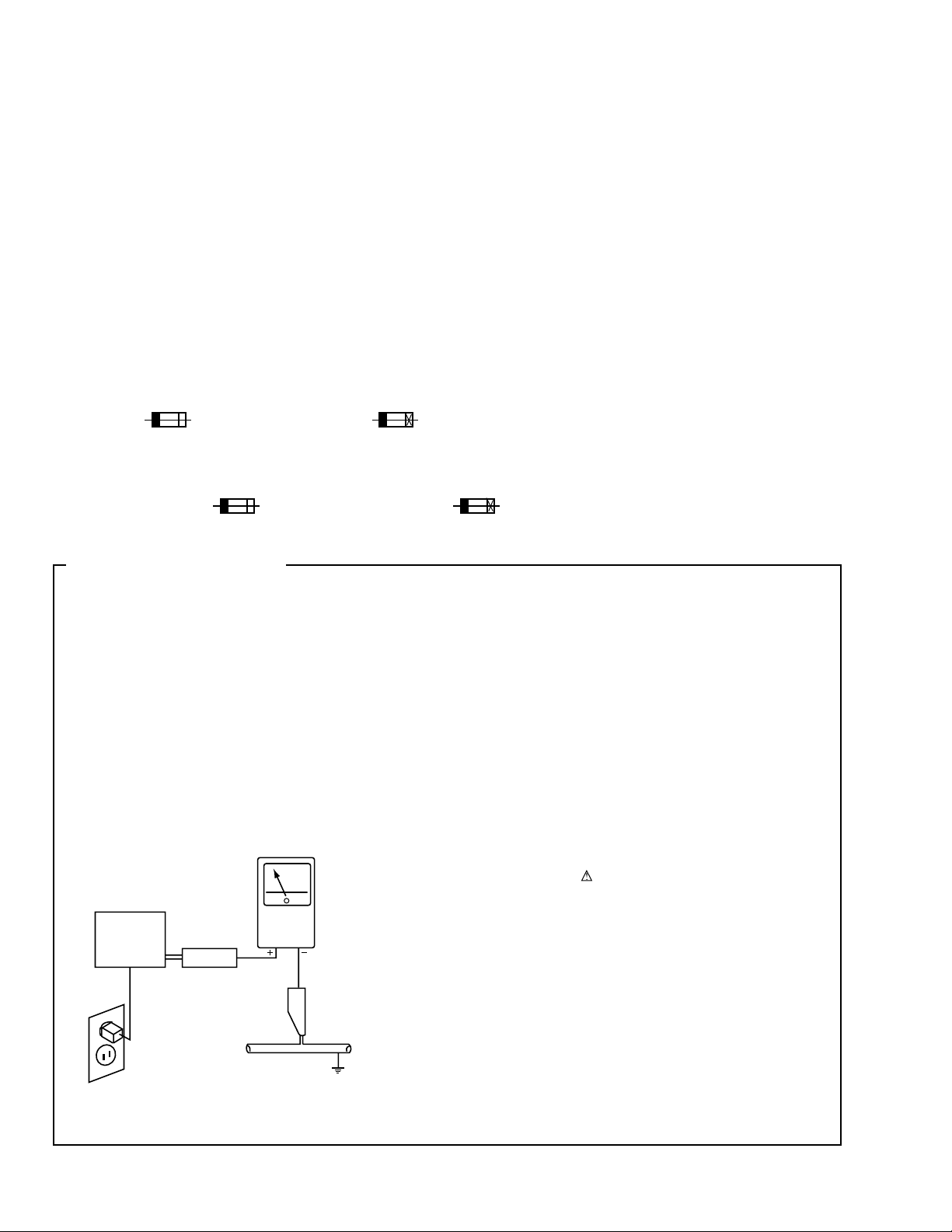
LEAKAGE CURRENT CHECK
Measure leakage current to a known earth ground (water
pipe, conduit, etc.) by connecting a leakage current tester
such as Simpson Model 229-2 or equivalent between the
earth ground and all exposed metal parts of the appliance
(input/output terminals, screwheads, metal overlays, control
shaft, etc.). Plug the AC line cord of the appliance directly
into a 120V AC 60Hz outlet and turn the AC power switch
on. Any current measured must not exceed 0.5mA.
Reading should
not be above
0.5mA
Earth
ground
Device
under
test
Also test with
plug reversed
(Using AC adapter
plug as required)
Leakage
current
tester
Test all
exposed metal
surfaces
ANY MEASUREMENTS NOT WITHIN THE LIMITS
OUTLINED ABOVE ARE INDICATIVE OF A POTENTIAL
SHOCK HAZARD AND MUST BE CORRECTED BEFORE
RETURNING THE APPLIANCE TO THE CUSTOMER.
2. PRODUCT SAFETY NOTICE
Many electrical and mechanical parts in the appliance
have special safety related characteristics. These are
often not evident from visual inspection nor the protection
afforded by them necessarily can be obtained by using
replacement components rated for voltage, wattage, etc.
Replacement parts which have these special safety
characteristics are identified in this Service Manual.
Electrical components having such features are identified
by marking with a
in this Service Manual.
The use of a substitute replacement component which does
not have the same safety characteristics as the PIONEER
recommended replacement one, shown in the parts list in
this Service Manual, may create shock, fire, or other hazards.
Product Safety is continuously under review and new
instructions are issued from time to time. For the latest
information, always consult the current PIONEER Service
Manual. A subscription to, or additional copies of, PIONEER
Service Manual may be obtained at a nominal charge from
PIONEER.
on the schematics and on the parts list
AC Leakage Test
2
Page 3

DV-K303C
THE AEL (ACCESSIBLE EMISSION LEVEL) OF THE LASER POWER OUTPUT IS LESS THAN CLASS 1
BUT THE LASER COMPONENT IS CAPABLE OF EMITTING RADIATION EXCEEDING THE LIMIT FOR
CLASS 1.
A SPECIALLY INSTRUCTED PERSON SHOULD DO SERVICING OPERATION OF THE APPARATUS.
LASER DIODE CHARACTERISTICS
FOR DVD : MAXIMUM OUTPUT POWER : 5 mW
WAVELENGTH : 655 nm
FOR CD : MAXIMUM OUTPUT POWER : 5 mW
WAVELENGTH : 785 nm
WARNING !
Additional Laser Caution
1. Inside detection switch (S201 on the SMEB assy) and loadingstatus detection switch (S9503 on the MOT OR assy) are detected
by the microprocessor (IC11 in the DVDM assy).
• To permit the laser diode to oscillate, it is required to set the
inside detection switch for the inside position (S201 : ON) and to
set the loading-status detection switch for the clamp position (the
center terminal of S9503 is shorted to +5V). The 655 nm laser
diode for DVD oscillation will continue if pin 19 of IC1 is shorted
to +5V (fault condition) in the DVDM assy.
The 785 nm laser diode for CD oscillates if pin 20 of IC1 is shorted
to +5V in the DVDM assy.
In the test mode ∗ , the laser diode oscillates when microprocessor detects a PLAY signal, or when the PLAY key is pressed
(S131 ON in the FLKY assy), with the above requirements satisfied.
2. When the cover is open, close viewing through the objective lens
with the naked eye will cause exposure to the laser beam.
∗ : See page 47.
3
Page 4
DV-K303C
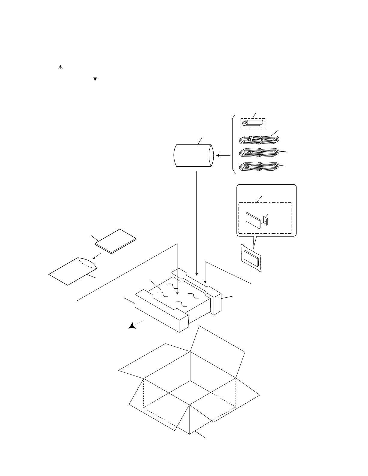
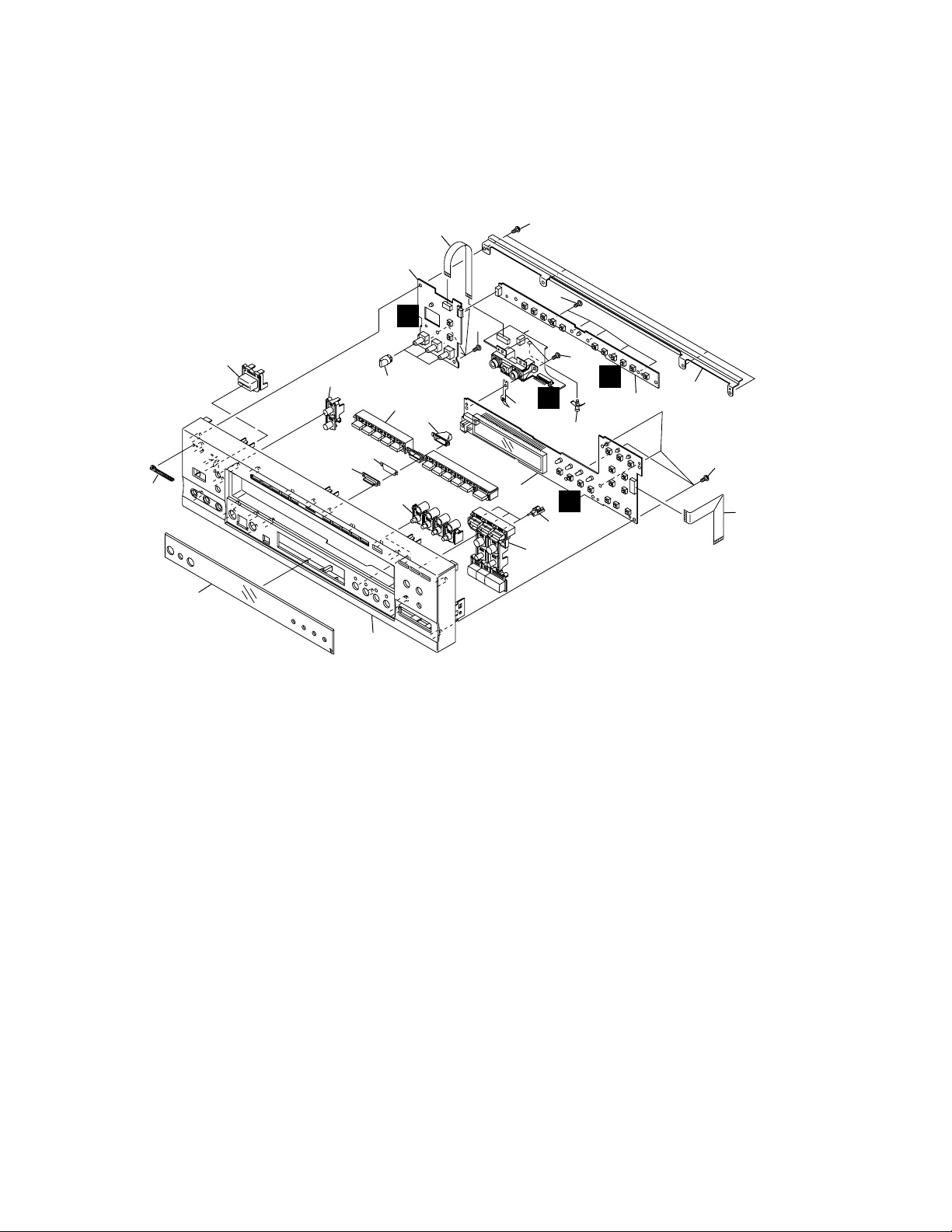
2. EXPLODED VIEWS AND PARTS LIST
NOTES:• Parts marked by "NSP" are generally unavailable because they are not in our Master Spare Parts List.
2.1 PACKING
The mark found on some component parts indicates the importance of the safety factor of the part.
•
Therefore, when replacing, be sure to use parts of identical designation.
Screws adjacent to mark on the product are used for disassembly.
•
4
8
9
5
8
11
7
12
3
2
1
10
FRONT
6
4
Page 5

PACKING PARTS LIST
Mark No. Description Part No.
DV-K303C
1 Power Cord ADG1154
NSP 4 Dry Cell Battery (R6P, AA) VEM1010
2 Video Cord (L = 1.5m) VDE1055
3 Audio Cord (L = 1.5m) VDE1054
5 Operating Instructions VRD1136
(English/Trad-Chinese)
6 Packing Case VHG2065
7 Sheet RHX1006
8 Polyethylene Bag VHL1051
9 Remote Control Unit VXX2761
10 Battery Cover AZA7204
11 Pad F VHA1240
12 Pad R VHA1241
5
Page 6
DV-K303C
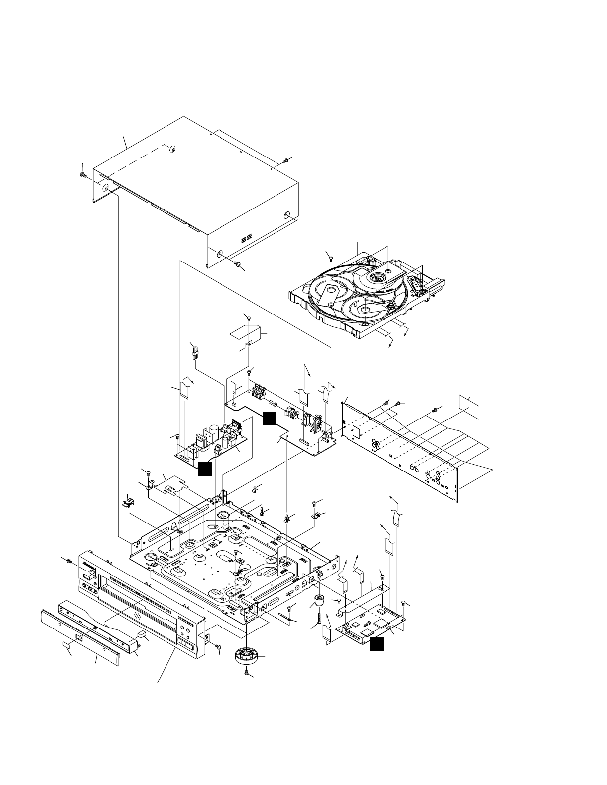
2.2 EXTERIOR SECTION
11
32
20
14
31
15
31
31
Refer to "2.4 $M MECHA DVD ASSY".
5
31
32
37
38
A
8
36
31
9
D
E
7
6
12
C
B
31
31
44
31
K
4
2
L
22
21
23
31
18
E
D
13
34
27
30
31
18
29
28
Refer to "2.3 FRONT PANEL SECTION".
34
31
26
31
24
25
37
A
33
C
B
31
17
31
1
F
6
Page 7

EXTERIOR SECTION PARTS LIST
Mark No. Description Part No.
1 DVDM Assy VWS1443
2 KRJB Assy VWV1834
4 POWER SUPPLY Unit VWR1313
NSP 5 $M MECHA DVD Assy VWT1163
NSP 13 Chassis VNA2146
NSP 14 PCB Base RNE1221
NSP 18 PCB Holder VNE2209
3 • • • • •
6 Flexible Cable (26P) VDA1695
(DVDM CN50 ↔ KRJB CN901)
7 Flexible Cable (16P) VDA1736
(DVDM CN40 ↔ KRJB CN501)
8 Flexible Cable (26P) VDA1705
(DVDM CN2 ↔ POWER SUPPLY CN201)
9 Flexible Cable (5P) VDA1737
(KRJB CN401 ↔ MICB CN402)
10 • • • • •
11 Bonnet S VXX2617
12 Rear Panel VNA2310
15 FFC Binder VEC2020
16 • • • • •
17 FFC Holder VEC2075
19 • • • • •
20 Flat Cable Clip VEC2018
DV-K303C
NSP 21 PCB Holder PNW2029
NSP 22 Card Spacer DEC1770
NSP 23 PCB Holder PNW2100
NSP 38 Housing Assy VKP2189
NSP 39 • • • • •
24 Cord Clamper RNH-184
25 Insulator Assy VXA1638
26 Insulator Assy VXA2356
27 DVD Plate VAM1128
28 Tray Panel Base VNK4382
29 Tray Panel Cushion VEB1308
30 Tray Panel VNK4852
31 Screw BBZ30P080FMC
32 Screw BCZ40P060FNI
33 Screw BBZ30P180FMC
34 Screw IBZ30P080FMC
35 • • • • •
36 IC Guard VEC2098
37 Nyron Rivet VEC2040
40 • • • • •
41 • • • • •
42 • • • • •
43 • • • • •
44 Label VRW1872
7
Page 8
DV-K303C
2.3 FRONT PANEL SECTION
22
1
24
24
4
J
12
11(2/2)
G
23
24
H
2
21
24
18
20
3
I
10
11(1/2)
14
7
6
15
19
16
17
13
5
24
8
Page 9

FRONT PANEL SECTION PARTS LIST
Mark No. Description Part No.
DV-K303C
NSP 2 KYLB Assy VWG2068
NSP 3 PWSB Assy VWG2069
1 FLKY Assy VWG2064
4 MICB Assy VWV1679
5 Front Panel VNK4855
6 FL Lens VAH1382
7 Name Plate PAM1779
8 • • • • •
9 • • • • •
10 PW Button VNK4059
11 Main Key VNK4854
12 LED Lens VNK4503
13 4 Key VNK4502
14 Illumination Lens VNK4264
15 Illumination Filter VEC1983
16 11 Key VNK4853
17 Illumination Holder VNK4265
18 Flexible Cable (15P) VDA1738
(FLKY CN101 ↔ DVDM CN10)
19 Rotary Knob RAC2201
20 Flexible Cable (15P) VDA1734
(MICB CN403 ↔ PWSB CN301)
21 FP Angle VNE2159
22 Earth Plate VBK1093
23 Card Spacer DEC1772
24 Screw BBZ30P080FMC
9
Page 10
DV-K303C
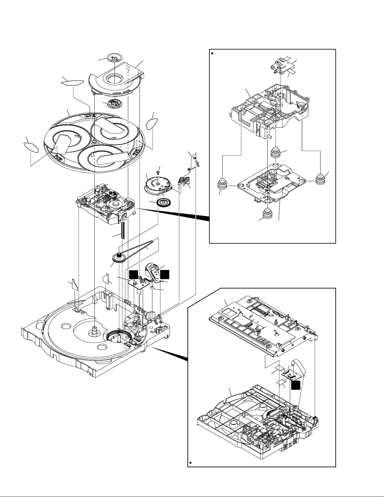
2.5 $M MECHA DVD ASSY
31(1/3)
31(2/3)
17
21
23
25
31(3/3)
16
29
12
14
15
8
Bottom View
10
27
10
4
24
7
9
Refer to
"2.5 TRAVERSE
MECHANISM ASSY".
9
30
13
30
11
28
A
1
C
18
3
22
2
6
26
B
5
10
Bottom View
Page 11
$M MECHA DVD ASSY PARTS LIST
Mark No. Description Part No.
NSP 1 SW Assy VWG2002
NSP 2 TRADE Assy VWG2003
NSP 3 MOTOR Assy VWG2004
4 TRAVERSE Mechanism Assy-SVXX2653
5 Flexible Cable (8P) VDA1715
(TRADE CN9001 ↔ SMEB CN202)
6 Flexible Cable (13P) VDA1716
(TRADE CN9002 ↔ DVDM CN3)
7 Flexible Cable (24P) VDA1704
(Pickup Assy ↔ DVDM CN4)
8 Servo Spring ABH7126
9 Float Rubber C VEB1301
10 Float Rubber B AEB7066
11 Belt AEB7072
12 Main Cam ANW7093
13 Gear Pulley ANW7094
14 Lock Lever ANW7095
15 Planet Gear ANW7096
16 Actuator ANW7097
17 Rotary Tray ANW7113
18 Motor Pulley PNW1634
19 • • • • •
20 • • • • •
DV-K303C
21 Clamper Plate VNE2162
22 Mecha Base VNK4600
23 Clamper VNK1738
24 FFC Holder VNL1803
25 Clamper Holder VNL1804
26 Loading Tray XNW3002
27 Servo Base XNW3012
28 Slider Motor (LOADING) VXM1033
29 Screw IPZ30P080FMC
30 Shaft Press Rubber VEB1300
31 Tray Number Label VRW1759
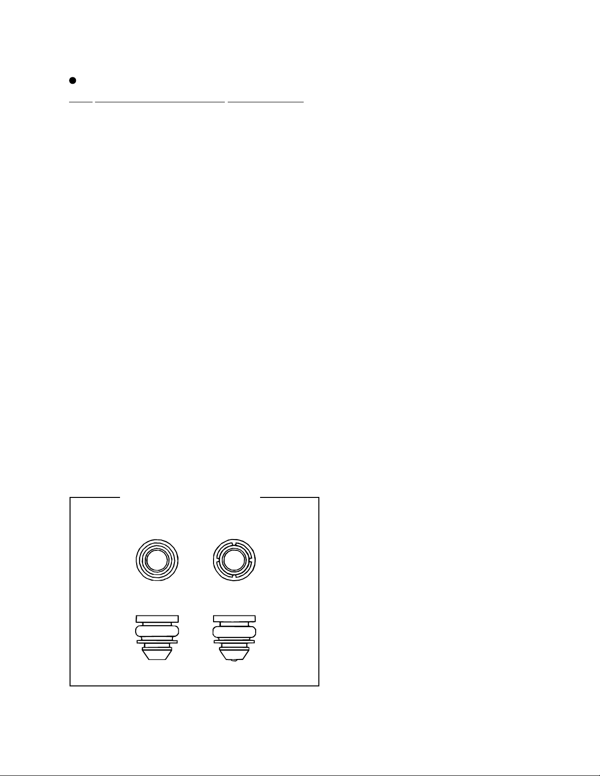
Detail of Float Rubber
(No.9, No.10)
AEB7066
VEB1301
(Soft) (Hard)
11
Page 12
DV-K303C
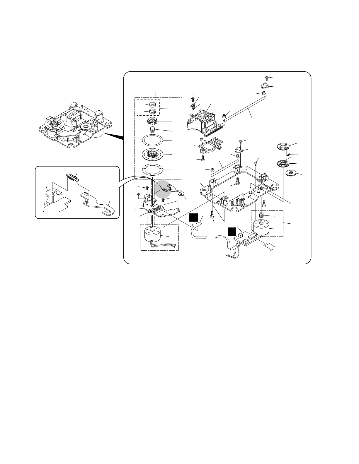
2.6 TRAVERSE MECHANISM ASSY-S
• Top View
17
37
18
26
11
25
27
7
29
36
3
22
33
21
33
E
23
28
10
15
10
5
10
13
37
10
14
7
2
7
18
32
1
D
35
30
16
9
31
37
21
17
24
34
19
8
6
20
12
9
37
4
12
Page 13

TRAVERSE MECHANISM ASSY-S PARTS LIST
Mark No. Description Part No.
NSP 1 SMEB Assy VWG2048
NSP 2 FGSB Assy VWG2009
NSP 3 Motor (CARRIAGE) VXM1079
NSP 4 Motor (SPINDLE) VXM1084 (or VXM1078)
NSP 5 Pickup Assy VWY1055
6 Table Sheet DEC2040
7 Screw VBA1058
8 Centering Spring VBH1278
9 Hook Spring VBH1317
10 Skew Spring VBH1303
DV-K303C
NSP 12 Reflected Sheet VEC1959
NSP 16 Magnet Holder VNE2070
NSP 17 Motor Base VNE2154
NSP 18 Cover VNE2155
NSP 20 Disc Table VNL1747
NSP 30 Magnet VYM1024
11 Gear Spring VBH1308
13 Guide Bar VLL1516
14 Sub-guide Bar VLL1517
15 Hold Spring VNC1017
19 Centering Ring VNL1746
21 Hook VNL1770
22 FFC Holder VNL1802
23 Mechanism Base VNL1806
24 FG Holder VNL1807
25 Gear A VNL1808
26 Gear B VNL1809
27 Gear C VNL1810
28 Slider VNL1811
29 Gear D VNL1814
31 Screw JFZ17P025FZK
32 Screw JGZ17P028FMC
33 Screw VBA1051
34 Magnet Holder Assy VXX2507
35 Spindle Motor Assy VXX2649
36 Carriage Motor Assy VXX2650
37 Screw PBA1069
13
Page 14
1
23
DV-K303C
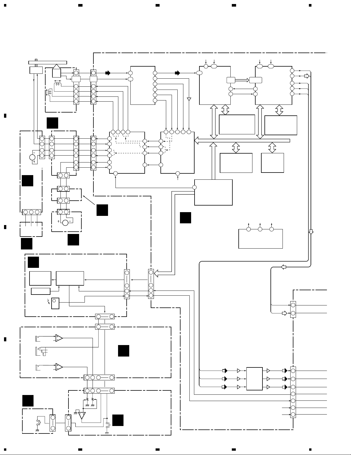
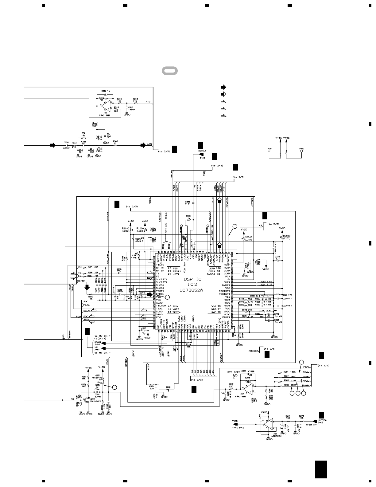
3. BLOCK DIAGRAM AND SCHEMATIC DIAGRAM
3.1 BLOCK DIAGRAM
4
27M
A
SPDL
MOTOR
OEIC
FCS
TRKG
PICKUP
ASSY
B
CN9001
(8P)
2
7
1
8
4
5
6
3
M
CN202
(8P)
CARRIAGE
B
MOTOR
D
SMEB
ASSY
2 13
LOADING MOTOR
FGSB
E
ASSY
G
FLKY ASSY
FL TUBE
V101
C
VAW1050
KEY SW
REMOTE
SENSOR
(24P)
15
18,19
22,23
4
1
3
2
TRADE
ASSY
12
12
21
21
M
(13P)
CN9002
8
10
6
4
7
9
CN9501
J9501
J9502
J9502
C
FL CONTROL
IC101
PE5141A
(24P)
CN4
10
7,6,
3,2
F_RTN
21
F_DRV
24
T_DRV
22
T_RTN
23
(13P)
CN30
SPDL+
8
SPDL-
10
SLDR_R
6
SLDR_F
4
LOAD+
7
LOAD-
9
(6P)
(6P)
(4P)
(4P)
A
MOTOR
ASSY
1 10
B1-B4
13 12 10 9
31
32
14
15
SPDL & FTS
DRIVER
34
35
M56788FP
37
LODDRV
SW
ASSY
(15P)
CN101
CN104
(10P)
RFRF
3 54
6-9
LA9701M
IC3
15
4
SEL IR
3
2
RF IC
IC1
3
20
17
28 46
IR
46
56
57
42
35
FDO
TDO
SLDO
SPDO
(15P)
CN10
1
12
13
14
RFO
DSPRF
BH
PH
FE
TE
32 33 30 31 39
47
48
45
SERVO DSP
LC78652W
16M
Q105
IC2
14
42
F
DVDM ASSY
16M
107
4
170
DVD
DECODER
MY CHIP
IC12
PD4995A
SYSTEM
CONTROL CPU
IC11
PD3410A
SD0-SD7
57-60
63-66
SREQ
56
XSACK
55
4M DRAM
IC15
MN414800CSJ-07
WORK SRAM
(1M)
IC14
TC55V1001AF8
27M
36/16M
197
205
MPEG2
78,80-84
DECODER
86,87
AV-1
91
IC18
89
MB86373
16M SDRAM
IC19
MB811171622A
-100FN
FLASH
MEMORY
IC13
VYW1776
27M
16M536/16M
6
1
CLOCK GENERATOR
IC21
CY2081SL-638
ADAI(AC3)
ADAO
ADAI(AC3)
64
ADAO
62
VOUT
45
YOUT
39
COUT
36
CN50
6
7
(26P)
1 10
3
1
MIC1
MIC
CONTROL
MIC2
D
H
KYLB
ASSY
2
IC401(2/2)
NJM2068M
IC401(1/2)
5
6
CN201 CN302
1
4
7
164 15
11012 15
5
6
1
7
4
CN401(10P)
J
MICB ASSY
CN403(15P)
CN303(DV-C302D: 9P)
CN301(DV-K302CD: 15P)
PWSB
I
ASSY
VOUT
YOUT
COUT
(V/Cb)
(C/Cr)
(16P)
F1
Q83
(Y)
Q81
Q85
VIDEO
FILTER
Q84
Q82
Q86
(V/Cb)
(Y)
(C/Cr)
V+5D
V+12D
10
12
8
5
4
3
2
CN40
V/Cb/S
Y
C/Cr
SEL IR
IR
14
1234
Page 15
5
678
DV-K303C
M + 6V
+12V
+12V
+5V
V2R5 +3.3V
PQ2TZ15
IC401
IO
REG
EV+5V
– 27V
(26P)
CN2
(26P)
1,2
10
12
13
16
22
26
CN201
1,2
5
5
7
7
10
|
|
12
13
|
|
16
22
26
POWER
L
SUPPLY
UNIT
CN101
1
2
LIVE
NEUTRAL
AC IN
: RF Signal Route
: Audio Signal Route (L ch)
(V/Cb)
: V/Cb Signal Route
(Y)
: Y Signal Route
(C/Cr)
: C/Cr Signal Route
A
B
21
20
7
5
9
12
13
14
15
CN901
(26P)
(16P)
CN501
V+5D
V+12D
TC74HCT7007AF
JA601
CONTROL
IN
Q801
TC9409BF-001
IC901
(V/Cb)
(Y)
(C/Cr)
NJM78L08A
IC199
I
REG
311128
IC401
V+8V
O
JA802
OPTICAL AC-3/PCM
JA801
COAXIAL
IC402
TC74HC157AF
10
DIGITAL
AUDIO
OUT
9
K
KRJB ASSY
(V/Cb)
(Y)
(C/Cr)
IC301
PCM1716E
2
3IN 6OUT
VIDEO AMP
AIN
3
BIN
6
CIN
10
IC501
LA7138M
AMP
AMP
AMP
16
13
IC101(2/2)
IC101(1/2)
23
21
19
17
15
13
IC101
BA4560F
2
3
5
6
1
L1
L2
JA101
AUDIO OUT
7
(V)
(Y)
(C)
(C/Cr)
(V/Cb)
(Y)
R1
R2
JA504
COMPOSITE
VIDEO OUT
3
4
P
P
Y
(2CH)
JA504
S VIDEO
OUTPUT
R
COMPONENT
VIDEO
B
OUT
C
D
JA503
15
5
6
7
8
Page 16
1
23
4
DV-K303C
3.2 SW, TRADE, MOTOR, SMEB, FGSB ASSYS
and OVERALL WIRING DIAGRAMS
Note : When ordering service parts, be sure to refer to "EXPLODED VIEWS and PARTS LIST" or "PCB PARTS LIST".
A
KRJB ASSY
K
B
(VWV1834)
C
PWSB ASSY
I
(VWG2069)
D
MICB ASSY
J
(VWV1679)
KYLB ASSY
H
(VWG2068)
FLKY ASSY
(VWG2064)
G
16
1234
Page 17
5
678
DV-K303C
: RF SIGNAL ROUTE
(F)
: FOCUS SERVO LOOP LINE
POWER SUPPLY UNIT
(VWR1313)
L
(T)
: TRACKING SERVO LOOP LINE
(S)
: SLIDER SERVO LOOP LINE
AC110-127/220-240V
50/60Hz
POWER CORD
: ADG1154
A
F 1/3- F 3/3
F
DVDM ASSY (VWS1443)
(T)
(F)
(F)
(F)
(F)
(T)
(T)
PICKUP ASSY
(F)
(F)
(T)
(VWY1055)
TRAVERSE MECHANISM
ASSY-S (VXX2653)
B
FGSB ASSY
E
(VWG2009)
TRADE ASSY
B
(VWG2003)
(S)
(S)
(S)
(S)
CARRIAGE
MOTOR
ASSY
: VXX2650
C
SPINDLE
MOTOR
ASSY
: VXX2649
D
SMEB ASSY
(VWG2048)
VXM1033
D
C
MOTOR ASSY
(VWG2004)
5
6
7
SW ASSY
A
(VWG2002)
DCBA
E
8
17
Page 18

1
DV-K303C
3.3 DVDM ASSY (1/3)
23
4
F 1/3
A
B
CN201
L
DVDM ASSY (VWS1443)
CN2
VKN1479
CN4
VKN1464
R11-R14:560
F
FOFST
(T)
(F)
(F)
2/3
(F)
F
2/3
(F)
(T)
(T)
1
SH_2
F
2/3
1/2
F
2/3
(DVD) (DVD)
(CD)
(CD)
(DVD) (DVD)
(CD)
(F)
(T)
(T)
(T)
(F)
2
4
(T)
F
2/3
C
(F)
(T)
(F)
SH_1
F
2/3
F
2/3
PICKUP ASSY
(F)
(T)
(T)
(F)
CN30
VKN1472
D
CN9002
B
18
F
(S)
(S)
1/3
1234
(F)
(T)
(T)
(F)
(S)
(S)
SH_3
(F)
(F)
(F)
F
2/3
(F)
(T)(T)(S)
(S)
(S)
(T)
(T)
(S)
Page 19
5
678
DV-K303C
A
: The power supply is shown with the marked box.
: RF SIGNAL ROUTE
: ROM DATA SIGNAL ROUTE
(F)
2/2
: FOCUS SERVO LOOP LINE
(T)
: TRACKING SERVO LOOP LINE
(S)
: SLIDER SERVO LOOP LINE
(DVD) (DVD)
SH_4
F
2/3
(T)
(F)
(CD)
(S) (S)
(F)
(T)
F
2/3
F
MY_4
F
2/3
(T)
(F)
(CD)
5
(F)
(T)
3/3
F
2/3
MY_5
F
2/3
MY_2
6
R1
10k
F
2/3
ADDRESS
R3
10k
B
C
RESET
F
2/3
8
7
5
6
DATABUS
F
2/3
2/2
1/2
7
1011
F
2/3
MY_3
9
F
2/3
D
F
1/3
8
19
Page 20

1
DV-K303C
3.4 DVDM ASSY (2/3)
23
4
F 2/3
A
B
F
3/3
AV1_1
DVDM ASSY (VWS1443)
VYW1776
F
3/3
MY_1
F
3/3
F
1/3
F
3/3
F
3/3
F
1/3
MY_5
C
F
1/3
F
1/3
3
F
1/3
MY_4
F
3/3
F
1/3
MY_3
D
20
F
3/3
F
3/3
AV1_2
2/3
F
1234
MY_2
F
1/3
Page 21
5
678
DV-K303C
: The power supply is shown with the marked box.
F
ADDRESS
F
3/3
SH_7
(20MHz)
F
3/3
1/3, 3/3
: ROM DATA SIGNAL ROUTE
: AUDIO SIGNAL ROUTE
F
1/3, 3/3
DATABUS
F
3/3
SH_5
A
B
5→3 CONVERTER
3→5 CONVERTER
F
1/3
FOFST
SH_4
F
1/3
SH_1
F
F
1/3
SH_2
F
3/3
1/3
SH_3
F
1/3
C
CN10
F
1/3
VKN1474
CN101
F
1/3
F
1/3, 3/3
G
D
F
F
1/3
5
1/3
6
7
SW+5
IR
R686
F
3/3
0
F
SW+5
2/3
8
21
Page 22
1
DV-K303C
3.5 DVDM ASSY (3/3)
23
4
A
F 3/3
ADDRESS
F
2/3
B
DVDM ASSY (VWS1443)
SH_5
F
2/3
DATABUS
F
2/3
F
2/3
AV1_1
R841
22X4
DCN1104
AV1_2
E
2/3
C
F
2/3
F
2/3
D
(C)
(Y)
(Y)
(C)
(V/CB)
12 15 13 16 14 17
(V/CB) (V/CB)
(Y)
(C)
22
3/3
F
1234
Page 23
5
678
DV-K303C
A
F
2/3
: AUDIO SIGNAL ROUTE
: ROM DATA SIGNAL ROUTE
(V/CB)
: V/CB SIGNAL ROUTE
(Y)
F
2/3
F
2/3
F
1/3
: Y SIGNAL ROUTE
(C)
: C SIGNAL ROUTE
B
(V/CB)
(C)
L917
VTL1078
SH_7
F
2/3
R927 0
R872 0
R873 0
R874 0
R875 0
R876 0
R877 0
R878 0
R879 0
R880 0
R881 0
F
ADA1
ADA2
ADA3
2/3
6CHMD
LFEON
DTSMD
XCSDF2
XCSDF1
AUDRST
F
2/3
MY_1
DFSI
(V/CB)
160F
2SA1576A
(V/CB)
(Y)
160F
160F
(Y)
2SA1576A
(C)
2SA1576A
2SA1576A
2SA1576A
2SA1576A
RESET
(Y)
(C)
F
2/3
(Y)
(V/CB) (V/CB)
CN50
VKN1479
3V
6CH/X2CH
LFEON
ADA1(FL/FR)
ADA2(C/LFE)
ADA3(LS/RS)
N.C.
DSP THRU
MIC ON2
DSP
MIC ON1
48/44
SDATA
SCLK
XRESET
XMUTE
DACXCS
SCK
LRCK
ADA0(L/R)
AC3/PCM
GNDD
DAC CLK
GNDD
5V
12V
CN40
VKN1475
(Y)
CN901
K
C
R903 0
R904 0
(C)
V+5D
V+12D
XRESET
F
CN501
K
3/3
8
D
23
(C)
V+5DV+12D
F
2/3
5
6
7
Page 24
1
23
DV-K303C
3.6 FLKY, KYLB, PWSB and MICB ASSYS
G
A
CN101
CN10
F 2/3
FLKY ASSY
4
: The power supply is shown with the marked box.
(VWG2064)
B
KYLB ASSY
H
(VWG2068)
S201-S211: ASG7013
MICB ASSY
J
(VWV1679)
C
VKN1553
CN201CN302
CN301
CN403
PWSB ASSY
I
(VWG2069)
CN401 CN104
CN402
VKN1553
D
L
CN102
24
1234
JIHG
Page 25

5
SWITCHES
FLKY ASSY
S131 : 3
S132 : OPEN/CLOSE 0
S133 : DISC 3
S134 : DISC 2
S135 : DISC 1
S136 : DISC CHANGE
S137 : 41
FL DIMMER
678
DV-K303C
S138 : ¡¢
S139 : 8
S140 : 7
S158 : PLAYBACK CONTROL
S159 : KARAOKE MODE
S160 : ONE-TOUCH KARAOKE
S161 : FL DIMMER
KYLB ASSY
S201 : 1
S202 : 2
S203 : 3
S204 : 4
S205 : 5
S206 : 6
S207 : 7
S208 : 8
S209 : 9
S210 : 0
S211 : +10
PWSB ASSY
S300 : KEY CONTROL HIGH (#)
S301 : KEY CONTROL LOW ( )
S302 : STANDBY/ON
A
B
C
12k 15k
FL DIMMER
D
25
5
6
7
G
I
8
Page 26

1
DV-K303C
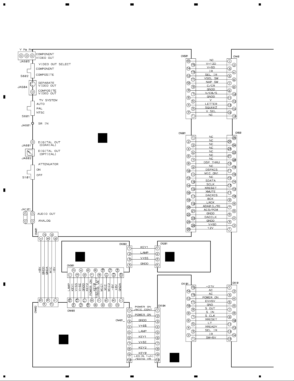
3.7 KRJB ASSY
A
CN501
23
K
KRJB ASSY (VWV1834)
(Y)
(V/CB)
4
P
B
P
R
(Y)
CN40
(V/CB)
(C)
F 3/3
CN901
B
(V/CB)
(C) (C)
(Y)
(V/CB)
(Y)
(Y)
(V/CB)
(C)
JA504
JA504
VKB1163-
CN50
F 3/3
C
CN401
D
CN402
J
26
K
1234
Page 27

5
678
DV-K303C
: The power supply is shown with the marked box.
: AUDIO SIGNAL ROUTE
(V/CB)
: V/CB SIGNAL ROUTE
(Y)
: Y SIGNAL ROUTE
(C)
: C SIGNAL ROUTE
A
B
C
D
K
5
6
7
8
27
Page 28

1
DV-K303C
3.8 POWER SUPPLY UNIT
23
4
A
NOTE OF SPARE PARTS IN POWER SUPPLY (SYPS) ASSY
• In case of repairing, use the described parts only to prevent an accident.
• Please write the red mark on the board when the primary section of POWER SUPPLY (SYPS) Unit is repaired.
• Please take care to keep the space, not touching other parts when replacing the parts.
POWER SUPPLY UNIT (VWR1313)
L
Q101
VZF1062
R110
C101
D108
VZF1045
Q103
VZF1062
C117
R101
C104
R105
D103
VZF1077
L101
413
FG101
C103
C105
C122
D107
1SS270A
2SC1740S
2
Q104
C102
R120
R108
R109
D109
(1/2)
VZF1071
D101
VZF1044
C110
Q102
2SC3377
D152
C153
S
BP FB
C154
L104
L103
C116
D104
MTZJ2.4B
C115
SD
IC151
SS
D153
R151
D151(1/2)
VZF1071
R111
R112R113
R116
D120
D105
1SS270A
C151
D102
EG01C
R114
D106
(1/2)
VZF1071
C112
R130
B
R131
C
CN101
YKE31-0120
1
AC IN
2
LIVE
NEUTRAL
CN102
12
C111
C120
F101 : 2A/250V (VEK1049)
F101
12
LIVE
NEUTRAL
D
VKP2189
T101
7
6
5
4
2
1
1
2
3
5
D110
1SS270A
C121
6
C107 C108
9
10
11
14
12
GND2
13
16
15
T102
10
8
28
L
1234
Page 29

5
678
DV-K303C
• NOTE FOR FUSE REPLACEMENT
CAUTION -
FOR CONTINUED PROTECTION AGAINST RISK OF FIRE.
REPLACE WITH SAME TYPE AND RATINGS ONLY.
L711
L211
39µH/1.3A
R201
47
VZF1065
VZF1065
VZF1076
VZF1075
D811
VZF1054
D211
D711
D311
D411
D412
D511
10ELS2
D611
D213
MTZJ15B
C311
330/35
R511
10
VZC1057
R611
33
VZC1060
C411
330/35
C211
330/35
C711
330/35
D106
(2/2)
VZF1071
IC201
AN1431T
L811
39µH/1.3A
R711
0.51 1/2W
VZC1061
R202
1k
C201
0.47/50
R203
1.5k
R204
330
R205
1.5k
IC311
VZF1078
IIO
GCT
IC411
VZF1074
GCT
D513
MTZJ8.2B
O
R412
680
C412
100/35
R514
10k
R411
1.2k
C212
100/35
C511
47/50
P211
VEK1041
1.0A/60V
C313
47/35
CN201
52806-2610
1 M+6V
M+6V
2
GND (M+6V, M+12V)
3
GND (M+6V, M+12V)
4
M+12V
5
GND (D+12V)
6
D+12V
7
GND (+5V)
8
GND (+5V)
9
+5V
10
+5V
11
+5V
12
+3.3V
13
+3.3V
14
+3.3V
15
+3.3V
16
GND
17
GND
18
GND
19
GND
20
GND
21
22
EV. +5V
P ON/OFF
23
FLAC
24
FLAC
25
-27V
26
CN2
1/3
F
A
B
C
C811
330/35
D151
(2/2)
VZF1071
IC801
AN1431T
R801
47
R802
1k
C801
0.47/50
R803
1.5k
R804
100
R805
1.5k
D109
(2/2)
VZF1071
Q801
R806
680
C611
0.01/50
C812
330/35
C612
0.01/50
D
CAUTION : FOR CONTINUED PROTECTION AGAINST RISK OF FIRE,
5
REPLACE ONLY WITH SAME TYPE NO. 491001 MFD. BY
LITTELFUSE INC. FOR P211.
6
L
7
8
29
Page 30

DV-K303C
WAVEFORMS
Note : The encircled numbers denote measuring point in the schematic diagram.
Measurement condition : No. 1 to 4 and 6 to 11 : Disc MA1, Title 1-chp 1
Foot of R169 (RF)
1
V: 100mV/div. H: 0.2µsec/div.
No. 5 : CD, ABEX-784 Track 1
No. 12 to 14 : MJK1, Title 1-chp 4
No. 15 to 17 : MJK1, Title 1-chp 5
Q281 - Collector (FG)
7
V: 1V/div. H: 5msec/div.
13
GND
IC18 - pin 39 (Y output)
V: 0.2V/div. H: 5msec/div.
CN7 - pin 5, 6 (RFO)
2
V: 500mV/div. H: 0.1µsec/div.
IC12 - pin 70 (MY CHIP input)
3
V: 1V/div. H: 0.2µsec/div.
CN7 - pin 9, 10 (Tracking Error)
4
(AI-Inner Tracking Off)
V: 500mV/div. H: 2msec/div.
GND
GND
GND
Foot of R261 (FPWM)
8
V: 1V/div. H: 5msec/div.
Foot of R262 (VPWM)
9
V: 1V/div. H: 5msec/div.
Foot of R263 (PPWM)
10
V: 1V/div. H: 5msec/div.
GND
GND
GND
IC18 - pin 6 (C output)
14
V: 0.2V/div. H: 5msec/div.
IC18 - pin 45 (CB output when
15
selecting color difference output)
V: 0.2V/div. H: 5msec/div.
IC18 - pin 39 (Y output when
16
selecting color difference output)
V: 0.2V/div. H: 5msec/div.
GND
GND
GND
GND
IC2 - pin 39 (EFM before slice)
5
V: 1V/div. H: 1µsec/div.
IC2 - pin 1 (EFM)
6
V: 1V/div. H: 0.2µsec/div.
30
GND
GND
Foot of R264 (RPWM)
11
V: 1V/div. H: 5msec/div.
IC18 - pin 45
12
(Composite Video output)
V: 2V/div. H: 1msec/div.
GND
GND
IC18 - pin 36 (CR output when
17
selecting color difference output)
V: 2V/div. H: 5msec/div.
Page 31

1
234
4. PCB CONNECTION DIAGRAM
DV-K303C
NOTE FOR PCB DIAGRAMS :
1. Part numbers in PCB diagrams match those in the schematic
diagrams.
2. A comparison between the main parts of PCB and schematic
diagrams is shown below.
Symbol In PCB
Diagrams
BCE
BCE
D
Symbol In Schematic
Diagrams
BCEBCE
BCE
DGGSS
BCE
DGS
Part Name
Transistor
Transistor
with resistor
Field effect
transistor
Resistor array
3-terminal
regulator
3. The parts mounted on this PCB include all necessary parts for
several destinations.
For further information for respective destinations, be sure to
check with the schematic diagram.
4. View point of PCB diagrams.
Connector
P.C.Board
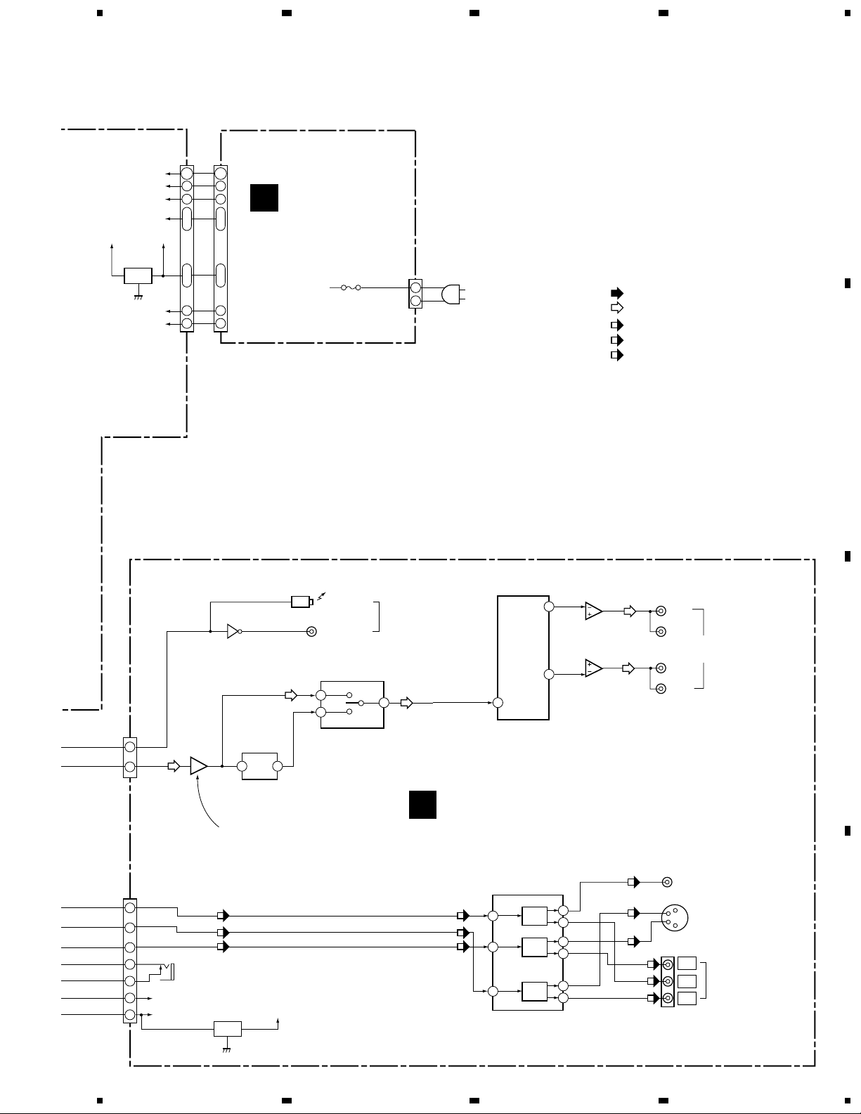
4.1 SW, TRADE, MOTOR, SMEB and FGSB ASSYS
MOTOR ASSY
C
Capacitor
Chip Part
A
SIDE A
SIDE B
B
F
CN30
B
CARRIAGE
MOTOR
M
(VNP1695-A)
TRADE ASSY
(VNP1685-A)
LOADING
MOTOR
M
SPINDLE
MOTOR
M
SW ASSY
A
PC101
R101
(VNP1685-A)
E
(VNP1685-A)
FGSB ASSY
C
D
SMEB ASSY
D
1
(VNP1784-A)
SIDE A
EDCBA
2
3
4
31
Page 32

1
DV-K303C
23
4
4.2 DVDM ASSY
A
B
DVDM ASSY
F
K
CN101
K
CN501
• This PCB is a four-layered board.
IC15
Q84
Q82
Q83
IC8
IC5
IC7
IC22
IC18
Q86
IC25
C
PICKUP
ASSY
B
CN9002
16M
VC1
Q109
Q101
IC1
Q102
IC3
Q106
IC11
Q103
Q7
IC401
Q6
D
(VNP1728-A)
CN201
L
G
CN101
SIDE A
32
F
1234
Page 33

1
234
DV-K303C
• This PCB is a four-layered board.
DVDM ASSY
F
Q88 Q90 Q92
Q87
Q89 Q91
IC12
IC26
A
B
(VNP1728-A)
IC19
IC21 IC2
IC27
Q112
IC17 IC16
Q114
Q113
IC14
Q1
IC13
Q3
Q107
Q108
C
Q105
Q251
D
SIDE B
F
1
2
3
4
33
Page 34

1
23
DV-K303C
4.3 FLKY, KYLB, PWSB and MICB ASSYS
PWSB ASSY
I
A
B
KYLB ASSY
H
4
(VNP1739-A)
C
FLKY ASSY
G
D
SIDE A
34
G H I
1234
Page 35

5
678
DV-K303C
A
(VNP1739-A)
J
MICB ASSY
B
(VNP1739-A)
K
CN401
F
CN10
C
D
(VNP1739-A)
IC102
G H J
5
6
7
8
35
Page 36

DV-K303C
C
A
1
23
4
KYLB ASSY
H
IC401
J
MICB ASSY
(VNP1739-A)
B
FLKY ASSY
G
C
D
Q102 Q103 Q104 Q105 I
36
H JG
1234
Page 37

5
678
DV-K303C
PWSB ASSY
I
A
(VNP1739-A)
Q301
IC301
B
(VNP1739-A)
IC101
C
D
SIDE B
(VNP1739-A)
G H I
5
6
7
8
37
Page 38

1
DV-K303C
4.4 KRJB ASSY
IC199 IC299 IC999
A
B
23
4
J
CN402
C
D
KRJB ASSY
K
38
Q121
Q111
Q123
Q122
Q221IC101
Q222 Q112 Q113
Q116IC301 IC304 IC401 IC402
K
1234
Page 39

5
678
DV-K303C
F
CN50
SIDE A
F
CN40
A
B
SIDE B
(VNP1830-A)
C
D
IC402 Q801
5
Q501
6
IC901
IC501
Q114Q400
K
7
8
39
Page 40

1
DV-K303C
4.5 POWER SUPPLY UNIT
23
4
A
AC IN
POWER SUPPLY
L
UNIT
LIVE
B
NEUTRAL
Q104
Q101
Q103
IC151
Q102
C
D
CN2
F
40
SIDE A
L
1234
Q801
IC801
IC201
IC411
IC311
Page 41

DV-K303C
Mark No. Description Part No.
Mark No. Description Part No.
5. PCB PARTS LIST
NOTES:•Parts marked by "NSP" are generally unavailable because they are not in our Master Spare Parts List.
The mark found on some component parts indicates the importance of the safety factor of the part.
•
Therefore, when replacing, be sure to use parts of identical designation.
When ordering resistors, first convert resistance values into code form as shown in the following examples.
•
Ex.1 When there are 2 effective digits (any digit apart from 0), such as 560 ohm and 47k ohm (tolerance is shown by J=5%,
and K=10%).
560 Ω→56 × 10
47k Ω→47 × 103→ 473 ........................................................RD1/4PU 4 7 3 J
0.5 Ω→R50 ..................................................................................... RN2H
1 Ω→1R0 ..................................................................................... RS1P
Ex.2 When there are 3 effective digits (such as in high precision metal film resistors).
5.62k Ω→ 562 × 10
Mark No. Description Part No.
LIST OF ASSEMBLIES
NSP $MECHA DVD ASSY VWT1163
NSP MECHA ASSY VWM1878
NSP SW ASSY VWG2002
NSP TRADE ASSY VWG2003
NSP MOTOR ASSY VWG2004
TRAVERSE MECH ASSY-S VXX2653
NSP SMEB ASSY VWG2048
NSP FGSB ASSY VWG2009
1
→ 561 ........................................................RD1/4PU 5 6 1 J
R 5 0
1 R 0
1
→ 5621 ......................................................RN1/4PC 5 6 2 1 F
Mark No. Description Part No.
MOTORASSY
SWITCHES AND RELAYS
S9503 ASG7009
OTHERS
J9502 4P JUMPERWIRE D20PWW0405E
K
K
DVDM ASSY VWS1443
KRJB ASSY VWV1834
NSP FRPB ASSY VWM1927
NSP KYLB ASSY VWG2068
NSP PWSB ASSY VWG2069
FLKY ASSY VWG2064
MICB ASSY VWV1679
POWER SUPPLY UNIT VWR1313
SW ASSY
SWITCHES ANDRELAYS
S9502 ASG7009
S9501 DSG1017
OTHERS
J9501 JUMPERWIRE D20PWY0610E
TRADE ASSY
OTHERS
CN9501 6P JUMPERCONNECTOR 52147-0610
CN9002 CONNECTOR SLW13R-1C7
CN9001 CONNECTOR SLW8R-1C7
SMEB ASSY
SWITCHES ANDRELAYS
S201 DSG1016
OTHERS
CN201 CONNECTOR 52044-0345
CN202 8P CONNECTOR VKN1212
PRINTED CIRCUIT BOARD VNP1695
FGSB ASSY
SEMICONDUCTORS
PC101 GP2S60
RESISTORS
All Resistors RS1/10S&&&J
DVDM ASSY
SEMICONDUCTORS
IC5, IC7 BA4510F
IC21 CY2081SL-638
IC14 KM68V1000CLG-7L
IC1 LA9701M
IC2 LC78652W
IC3 M56788FP-TFB
IC19
IC18 MB86373B
IC16 MC74VHC541DT
IC17 MC74VHCT541ADT
MB811171622A-100FN
41
Page 42

DV-K303C
Mark No. Description Part No.
IC15 MN414800CSJ-07
IC11 PD3410A
IC12 PE5108A
IC401 PQ2TZ15
IC23 TC7SH32FU
IC8 TC7SHU04F
IC13 VYW1776
Q106, Q109, Q81–Q86 2SA1576A
Q105, Q114, Q251 2SC4081
Q102 HN1A01F
Q103, Q281, Q6, Q7 HN1B04FU
Q101 HN1C01F
Q112, Q113 HN1C01FU
Q108 HN1K03FU
Q107 RN1902
Q3 RN1911
Q1 RN4982
D302 KV1471E
D6 RB501V-40
D665, D666 RB521S-30
COILS ANDFILTERS
F8500 CHIP BEAD DTF1069
L101, L150, L330 LCYA100J2520
L304 LCYA2R7J2520
F1 VIDEO FILTER VTF1155
L81 CHIP COIL(22.0µH) VTL1067
L917 CHIP BEADS VTL1078
CAPACITORS
C123, C145, C282, C613, C843 CCSRCH101J50
C322 CCSRCH120J50
C206, C210, C211 CCSRCH151J50
C126, C333, C845 CCSRCH180J50
C116, C151, C314 CCSRCH220J50
C152 CCSRCH221J50
C209 CCSRCH331J50
C104–C108, C134, C236 CCSRCH470J50
C122, C208 CCSRCH471J50
C128, C335 CCSRCH560J50
C127, C334 CCSRCH5R0C50
C124, C146 CCSRCH680J50
C117, C240, C352, C360 CCSRCH681J25
C129, C142 CEV101M10
C113, C139 CEV220M16
C413, C700, C808 CEV221M4
C111, C149, C205, C207, C401 CEV470M6R3
C403, C407 CEV470M6R3
C140, C223, C224, C252, C264 CKSQYB105K10
C312, C801, C802, C807 CKSQYB105K10
C809–C815, C817–C819 CKSQYB105K10
C229 CKSQYB224K16
C148, C217, C414 CKSQYF105Z16
C216, C313 CKSRYB102K50
C133, C136, C203, C220, C225 CKSRYB103K50
C239, C320, C321, C603, C625 CKSRYB103K50
C703, C711 CKSRYB103K50
C101, C102, C114, C118, C119 CKSRYB104K16
C121, C138, C204, C212, C213 CKSRYB104K16
C227, C228, C231, C263 CKSRYB104K16
Mark No. Description Part No.
C315–C317, C332, C804 CKSRYB104K16
C281, C354 CKSRYB222K50
C153, C266 CKSRYB223K25
C337 CKSRYB331K50
C214, C251, C261 CKSRYB472K50
C357 CKSRYB473K16
C330 CKSRYB682K50
C109, C110, C120, C130, C131 CKSRYF104Z16
C143, C150, C202, C215 CKSRYF104Z16
C221, C222, C226, C230, C235 CKSRYF104Z16
C265, C319, C327, C359, C367 CKSRYF104Z16
C369, C370, C402, C404, C406 CKSRYF104Z16
C408, C410, C412, C415 CKSRYF104Z16
C601, C602, C604–C612 CKSRYF104Z16
C614, C615, C617–C624, C626 CKSRYF104Z16
C701, C702, C704–C710 CKSRYF104Z16
C712–C726, C831–C833 CKSRYF104Z16
C837–C839 CKSRYF104Z16
C820, C821 (2.2µF) VCG1030
C299, C844 (0.47µF) VCG1032
C368, C409, C411 (47µF/16V) VCH1166
C405 (330µF/6.3V) VCH1191
VC1 (30pF) VCM1013
RESISTORS
R123 (39Ω×4) ACN7047
R732, R733, R735, R736 (47kΩ×4) ACN7077
R632 (100Ω×4) DCN1092
R608, R609, R613, R624, R627 DCN1094
(10kΩ×4)
R629, R631, R633, R634, R638 DCN1094
(10kΩ×4)
R654, R657, R658, R662, R664 DCN1094
(10kΩ×4)
R706, R717, R718 (10kΩ×4) DCN1094
R121, R663, R841 (22Ω×4) DCN1104
R712, R715, R840 (0Ω×4) DCN1106
R1020,R162, R2010,R2020,R2030 RS1/10S0R0J
R2040,R3050,R3520,R366, R4010 RS1/10S0R0J
R4020,R4030,R4040,R4050,R4060 RS1/10S0R0J
R667, R668, R671–R673 RS1/10S0R0J
R675, R676, R685, R686, R722 RS1/10S0R0J
R8000,R821, R8300,R8400 RS1/10S0R0J
R903, R904, R927 RS1/10S0R0J
R202 RS1/10S101J
R700 RS1/10S1R2J
R396 RS1/16S1001F
R807 RS1/16S1201F
R361, R364 RS1/16S1203F
R825–R827 RS1/16S1600F
R395 RS1/16S1801F
R363, R365 RS1/16S1803F
R805 RS1/16S2401F
R397, R806, R808 RS1/16S2701F
R848–R850 RS1/16S4700F
R164 RS1/16S5600F
R391 RS1/16S5601F
R394 RS1/16S6801F
R3510 (100Ω) VCN1120
Other Resistors RS1/16S&&&J
42
Page 43

DV-K303C
Mark No. Description Part No.
OTHERS
X 2 (20MHz) DSS1110
FLEXIBLE CABLE VDA1681
CN6 7P CONNECTOR VKN1299
CN7 CONNECTOR VKN1324
CN4 24P CONNECTOR VKN1464
CN10 15P CONNECTOR VKN1474
CN40 16P CONNECTOR VKN1475
CN30 13P CONNECTOR VKN1603
CN2, CN50 26P CONNECTOR VKN1616
X 1 (13.824MHz) VSS1129
FLKY ASSY
SEMICONDUCTORS
IC101 PE5141A
IC102 S-806D
Q102–Q105 PDTA124EK
D111, D115 MAY5064X
D112, D113 MPG5064X
D171, D174, D177 SLR-343DC(NPQ)
SWITCHES AND RELAYS
S131–S140, S158–S161 ASG7013
CAPACITORS
C105 CEJA470M10
C119 CKSQYB103K50
C104, C106, C114 CKSQYF104Z50
RESISTORS
R121, R122 RN1/10SE1001D
Other Resistors RS1/10S&&&J
Mark No. Description Part No.
PWSB ASSY
SEMICONDUCTORS
IC301 BA4560F
SWITCHES AND RELAYS
S300–S302 ASG7013
CAPACITORS
C303 CCSQSL121J50
C304, C305 CKSQYB103K50
C301 CKSQYB224K16
RESISTORS
VR301–VR303 (10KB) VCS1037
Other Resistors RS1/10S&&&J
OTHERS
CN302 CONNECTOR 4P 04P-FJ
CN301 15P CONNECTOR VKN1275
MICB ASSY
SEMICONDUCTORS
IC401 NJM2068M
CAPACITORS
C405, C408 CCSQSL121J50
C401, C402 CEJA470M10
C403, C404, C406, C409 CKSQYB103K50
C440, C441 CKSQYB105K10
C412 CKSQYF104Z50
OTHERS
CN104 BOTTOM CONNECTER BTMK10S-1S
REMOTE RECEIVER UNIT GP1U28X
V 101 FLTUBE VAW1050
SPACER VEC1599
CN101 15P CONNECTOR VKN1275
FL HOLDER VNF1096
X 101 (5MHZ) VSS1142
KYLB ASSY
SEMICONDUCTORS
Q201 DTD113ES
D201 MA111
SWITCHES AND RELAYS
S201–S211 ASG7013
RESISTORS
All Resistors RS1/10S&&&J
OTHERS
CN201 CONNECTOR 4P 04R-FJ
PL201 LAMP VEL1022
RESISTORS
All Resistors RS1/10S&&&J
OTHERS
CN402 CONNECTOR 52045-0545
CN401 BOTTOM CONNECTER BTMK10P-1R
PCB BINDER DEF1012
JA403 HEADPHONE JACK RKN1006
CN403 15P CONNECTOR VKN1246
JA401, JA402 MICJACK VKN1553
SNAP PLATE VNE1102
JACK HOLDER VNE2206
KRJB ASSY
SEMICONDUCTORS
IC101 BA4560F
IC999 IR3M03A
IC501 LA7138M
IC199 NJM78L08A
IC299 NJM79L08A
IC301 PCM1716E
IC402 TC74HC157AF
IC901 TC74HCT7007AF
IC304 TC7WU04F
IC401 TC9409BF-001
43
Page 44

DV-K303C
Mark No. Description Part No.
Q112, Q501 2PB709A
Q801 2SC2412K
Q111, Q121, Q221, Q222 2SD2114K
Q122 DTA124EK
Q113, Q114, Q116, Q123, Q400 DTC124EK
D601 1SS355
D199, D992 EP10QY03
COILS AND FILTERS
L909 LAU1R0J
L301 LAU2R2J
L999 LRCA470J
L801 COIL RTF1167
F304, F900
L501, L502 CHIP BEADS VTL1089
L992 (47µH) VTL1118
CHIP SOLID INDUCTOR
VTF1096
SWITCHES AND RELAYS
S101, S602 VSH1009
S601 VSH1020
CAPACITORS
C107, C207 CCSRCH331J50
C993 CCSRCH471J50
C399 CCSRCH560J50
C102, C202 CCSRCH561J50
C103, C203 CCSRCH820J50
C410, C434, C440, C442 CEAT101M10
C470, C471, C511, C801, C803 CEAT101M10
C902 CEAT101M10
C502, C504, C580, C590, C901 CEAT101M16
C966, C994 CEAT101M16
C805 CEAT1R0M50
C351, C380, C390 CEAT221M6R3
C101, C106, C201, C206, C311 CEAT470M10
C318 CEAT470M10
C105, C205 CEAT470M16
C512, C513, C516, C521, C540 CEAT471M6R3
C299, C999 CKSQYF225Z16
C403 CKSRYB102K50
C104, C204, C322, C404, C407 CKSRYB103K50
C421, C435 CKSRYB103K50
C340, C444, C503, C506, C510 CKSRYB104K16
C422 CKSRYB472K50
C199, C301, C308, C309, C315 CKSRYF104Z50
C320, C350, C401, C402, C415 CKSRYF104Z50
C417, C420, C424, C443, C501 CKSRYF104Z50
C505, C517, C520, C602, C802 CKSRYF104Z50
C804, C900 CKSRYF104Z50
RESISTORS
R104, R204 RN1/16SE1302D
R101, R201 RN1/16SE6201D
R292, R299, R929 RS1/10S122J
R995 RS1/10S1801F
R997, R998 RS1/10S1R2J
Mark No. Description Part No.
R500, R515, R518, R523 RS1/16S62R0F
Other Resistors RS1/16S&&&J
OTHERS
CN401 CONNECTOR 52045-0545
JA101 JACK DKB1033
JA802 OPTICAL LINK OUT GP1FA550TZ
JA601 JACK RKN1004
JA801 JACK VKB1121
JA504 JACK VKB1163
JA503 JACK VKB1165
CN501 16P CONNECTOR VKN1247
CN901 26P CONNECTOR VKN1257
SCREW PLATE VNE1948
PRINTED CIRCUIT BOARD VNP1830
POWER SUPPLY UNIT
SEMICONDUCTORS
IC201, IC801 AN1431T
IC411 VZF1074
IC311 VZF1078
Q104 2SC1740S
Q102 2SC3377
Q101, Q103 VZF1062
D511 10ELS2
D105, D107, D110, D514 1SS270A
D102 EG01C
D213 MTZJ15B
D104 MTZJ2.4B
D812 MTZJ6.8B
D513 MTZJ8.2B
D101 VZF1044
D108 VZF1045
D811 VZF1054
D211, D711 VZF1065
D106, D109, D151 VZF1071
D411 VZF1075
D311 VZF1076
D103 VZF1077
RESISTORS
R511 (10Ω) VZC1057
R611 (33Ω) VZC1060
R711 (0.51Ω, 1/2W) VZC1061
OTHERS
P 211 FUSE(1A) VEK1041
F101 FUSE(2A) VEK1049
44
R999 RS1/10S2200F
R113, R122, R949, R994 RS1/10S222J
R555 RS1/10S3R9J
R524, R528 RS1/16S1000F
R526, R530 RS1/16S1800F
Page 45

DV-K303C
6. ADJUSTMENT
6.1 ADJUSTMENT ITEMS AND LOCATION
Note : When the Traverse mechanism adjustment is not properly adjusted, jitter, error rate and play ability are defective.
The noise may come out by the case.
Adjustment Points (PCB Part)
DVDM ASSY
CN13
IC15
IC18
CN7
1, 2 : FE
3, 4 : GNDS
5, 6 : RFO
7 : SREQ
8 : 2.5V
9,10 : TE
11,12 : VREF
13 : VCODR
14 : FDO
CN1
CN4
CN3
IC3
IC1
16M
VC1
1
CN2
13
1
CN7
14
2
SIDE A
Adjustment Items
[Electrical Part]
Master Clock Adjustment
1
6.2 JIGS AND MEASURING
INSTRUMENTS
Frequency counter
Display digit ≥ 8-digit
1
Screwdriver (small)
6.3 NECESSARY ADJUSTMENT POINTS
When
EXCHANGE PCB ASSY
Exchange board
KRJB ASSY
Exchange board
DVDM ASSY
Mechanical
point
Electric
point
Mechanical
point
Electric
point
Note : is adjusted already.
Adjustment Points
45
Page 46

DV-K303C
6.4 ELECTRICAL ADJUSTMENT
1
Master Clock Adjustment
• When not properly adjusted : Uneven color
• Normal mode
• Power ON
START
DVDM ASSY
SIDE A
Player
16M
DVDM ASSY
16.934400MHz ± 80Hz
VC1
Frequency counter
46
Page 47

DV-K303C
7. GENERAL INFOMATION
7.1 DIAGNOSIS
7.1.1 TEST MODE SCREEN DISPLAY
TEST MODE SCREEN DISPLAY
When the test mode is entered, press the ESC button and the TEST button in order of the test mode remote control unit (GGF1067).
Consecutive double-OSD display is supported during test mode. The screen is composed 10 lines with a maximum of 32 characters per line.
It can't be used with the debugging display mode together.
• Screen Composition
Address
Background color
Tracking status and
Laser diode current value
Spindle status and AFB status
AGC setting
FTS servo IC information
C1 error value of CD and DVD
Internal operation mode of
the mechanism control
Disc judgment and
CD 1/3 beam switch
Equalizer value and
jitter value
Character in bold : Item name
: Information display
Test Mode Screen Display
(First Screen Display)
Caution :
The first screen and second screen switch by pressing [DISPLAY]
key of the remote control unit.
It is only a version display part on the lower right of the screen
those contents of display change.
ATB : ON/OFF information display and AGC manual setting display
deleted with the second generation.
The displays of Tilt error value, Tilt servo status and pickup
DVD/CLD display deleted with the third generation becomes LD
part is deleted.
Remote control code
Key code
Mechanism position value and
slider position
Output video system and
Skirt terminal output
AV1 chip version
FL controller version and
region setting for the player
FL controller destination setting
Port No. of Flash ROM and
system controller
Flash ROM version and Flash ROM size
System controller revision
DVD mechanism controller revision
(Control and part No. of GUI-ROM)
• Description of Each Item on the Display
(1) Address indication
The address being traced is displayed in number.
DVD : ID indication (hexadecimal number, 8 digits)
[ ∗ ∗ ∗ ∗ ∗ ∗ ∗ ∗ ]
CD : A-TIME (min. sec.) [ 0 0 0 0 ∗ ∗ ∗ ∗ ]
(Note : For DVDs, decimal-number indication is possible.)
(2) Code indication of the remote control unit [R – ∗ ∗ ∗ ∗]
The code for the key pressed on the remote control unit, which
is received by the FL controller, is displayed while the key is
pressed. In the case of the double code, the second code will
be displayed.
(3) Key code indication for the main unit [K – ∗ ∗ ]
The code for the key pressed on the main unit, which is
received by the system controller, is displayed while the key is
pressed.
(4) Background color indication [C – R∗ ∗ G∗ ∗ B∗ ∗]
(5) 1 Tracking status [TRKG – ∗∗∗]
Tracking on [ON ]
Tracking off [OFF]
2 Laser diode current value [LDI – ∗∗∗]
(6) 1 Spindle status [SPDL – ∗ ∗ ∗]
Spindle accelerator and brake, free-runnimg [A/B]
FG servo [FG]
Rough, velocity phase servo [SRV]
Offset addition, rough, velocity phase servo [O_S]
2 AFB status [AFB – ∗ ∗]
ON [ON ]
OFF [OFF]
(7) Mechanism position value [M – ∗]
Position code [1] to [3]
(8) Slider position [S – ∗ ∗ ∗ ∗]
CD TOC area [IN ]
CD active area [CD ]
(9) AGC setting [AGC – ∗ ∗]
AGC on [AGC-ON]
AGC off [AGC-OFF]
47
Page 48

DV-K303C
(10) Output video system [V – ∗ ∗ ∗ ∗]
NTSC system [NTSC]
PAL system [PAL ]
Auto-setting [AUTO]
Skirt terminal output [SK – ∗ ∗]
VIDEO [00]
S-VIDEO [01]
RGB [02]
Note : Display only the model which can do the output setting of
skirt terminal.
(11) FTS servo IC information
DSP coefficient indication [KS – [∗ ∗ ∗ ∗] ∗ ∗ ∗ ∗ ]
Displays the address (four digits) of the specified coefficient
and the setting value (four digits) with [TEST] and [9] keys.
(12) Error rate indication
1 C1 error value of CD [ER – C1 ∗ ∗ ∗ ∗ ]
2 C1 error value of DVD [ER – ∗ ∗ ∗ ∗ ∗ ∗ ∗ ∗ ]
(13) Internal operation mode of mechanism controller
[MM – ∗ ∗ : ∗ ∗]
Internal mechanism mode (2 digits) and internal mechanism
step (2 digits) of the mechanism controller
(14) 1 Disk sensing [DSC – ∗ ∗ ∗]
The type of discs loaded is displayed.
[DVD], [CD ], [VCD], [ ]
2 CD 1/3 beam switch [BM – ∗ ∗]
(20) 1 Version of the flash ROM [V : ∗ . ∗ ∗ ∗]
2 Flash ROM size [FLSH = ∗]
(21) Revision of the system controller [S : ∗ . ∗ ∗ ∗ / ∗ . ∗ ∗ ]
1 Revision number of the external ROM part (flash ROM) of
the system controller <Front>
2 Revision of the internal ROM part of the system controller
<Rear>
(22) Revision of the DVD mechanism controller
[M : ∗ . ∗ ∗ ∗]
Revision number of the external ROM part (flash ROM) of the
DVD mechanism controller
(23) Control and part numbers of the GUI-ROM
[GUI : ∗ ∗ ∗ ∗]
No GUI model displays as "––– / ––––".
OEM model displays the part number of GUI-ROM
[GUI : * * * *]
(15) 1 Equalizer value [E – ∗ ∗]
2 Jitter value [J – ∗ ∗]
nake the jitter four times, and renew it in every one
second. [4 – * *]
CD is effective only in the jitter value.
(16) Version of the AV-1 chip [ AV : ∗ . ∗ ∗' ∗' ]
(17) 1 Version of the FL controller [FL : ∗ ∗ ∗ ∗]
2 Region setting of the player [REG : ∗ ]
Setting value [1] to [6]
(18) Destination setting of the FL controller
[MDL : ∗ ∗ ∗ ∗ / ∗ ∗ ∗ ]
For charactors in front represent the type of model :
There charactors that follow represent the destination code.
J : /J, K : /KU, /KC, /KU/KC, R : /RAM, /RL, /RD, /LB,
WY : /WY
(19) The part number of the flash ROM and system
controller [∗ ∗ ∗ ∗ ∗ ∗ / ∗ ∗ ∗ ∗ ∗ ∗ ∗]
1 Part number of the flash ROM <Front>
(Example) VYW1536-A = W1536A
(Example) PD6256A9 = 6256A9
2 Part number of the system controller <Rear>
(Example) PD3381T1 = 3381T1
48
Page 49

7.1.2 TROUBLE SHOOTING
• No Power ON
• FL is not turned ON
• FL indication is unusual
DV-K303C
START
Turn on the power again
after 2 - 3 minutes.
Is FL turn on ?
Yes
Is the indication
of FL normal ?
Yes
Power ON
No
No
• Blow out fuse of the primary side
• Blow out micro-fuse on the POWER SUPPLY Unit. (Check the each voltage.)
(P211, R711)
• FL controller IC (IC101) on the FLKY Assy is damaged.
• Check the following connections :
POWER SUPPLY Assy - DVDM Assy
DVDM Assy - FLKY Assy
FLKY Assy - PWSB Assy
• Check each voltage (EV+5V, SW+5V, SW+3.3V, +6V and +12V)
(If above voltage are not supplied, check the micro-fuse.)
• Short or open the zenner diode
FL indication is dark or flickers.
Indicates the error message
• Blow out micro-fuse on the POWER SUPPLY Unit.
(R711)
on the POWER SUPPLY Unit.
(D513)
• Check the values of R118 on the
FLKY Assy.
Refer to the section "7.1.3 ERROR CODE".
Is tray open ?
Yes
Do the video and
sound come on ?
Yes
OK
No
No
• Check the connection between TRADE Assy and DVDM Assy.
(13P flexible cable)
• Check the +6V power supply voltage (above micro fuse).
Check the connection between KRJB Assy and DVDM Assy.
Indicate the error message.
Refer to the section "7.1.3 ERROR CODE".
49
Page 50

DV-K303C
7.1.3 ERROR CODE
yalpsiDLFsesuacelbissoPtinuehtfonoitarepO
REV1VA rellortnocmetsysfomargorpehthtiwhctamatonsipihc1-VA
RREAUPC).lausunusierawdraH(rorresserddaUPC noitarepooN
RREAAMD).lausunusierawdraH(rorresserddaAMD noitarepooN
DIHSALF
PRWHSALFMORhsalfehtfororretcetorpetirW noitarepooN
GISHSALF
MUSHSALF
EZISHSALF).tib-M8ro4esU(MORhsalfehtfororreeziS noitarepooN
LAGLLI
EVRESER).lausunusierawdraH(tpurretnidenifednU noitarepooN
TOLS ).lausunusierawdraH(deussidnammoctolsetairporppanI noitarepooN
).desu
).lausunusierawdraH(
).lausunusierawdraH(
)rorrerellortnocmsinahceM(
LF
11tuoemithcraeS
21
91
B1
22
32
33
83
rorre
elihw
rorre
AVLC
noitpircseD
rorrEfo
.sdnoces
yrterhcraeS
tuoemitgnicarT
gnigrevnoc
hcraes0xednI
fotuoemiT
renniredils
ecnerefmucric
fotuoemiT
retuoredils
ecnerefmucric
eslupKOFoN
kcabyalpgnirud
-isnes-epyt-csiD
rorregn
.epytcsideht
DVDahtiwfisesuaCDCahtiwfisesuaCtinUehtfonoitarepO
6(tuoemitfoesacaniro,semit
noitallatsniesreverroeruliafenilsubro,MOR
edocnoitareponanahtrehtoedocadehctefrellortnocmetsysehT
7nihtiwetelpmocebtondluochcraeS
.nacs
3retfadetelpmocebtondluochcraesA
4detucexesawpukcabhcraes,seirter
11gnicartsawtinuehtelihw)sdnoces
elihwtegratehtdnoyeberomroskcart
.gnigrevnocsawnoitarepohcraeseht
tagnicartelihw)sdnoces5.01(tuoemiT
.hcraesafoecnegrevnocfoegatseht
.tniopni
.detelpmocsaw
.sdnoces3nihtiwNOtondluochctiwsedisnI potS
.sdnoces2nihtiwFFOtondluochctiwsedisnI potS
.semit02ylsuounitnocdetaivedsawsucofehtnehW
ehtretnetondluoctidna,sdnoces
02(sdnoces3nihtiwdetelpmoceb
tinulortnocetomerehtgnisutuohtiwyalpsidLFehtnodeyalpsideratahtsedocrorrE
.oiduacificepseht
hsalfehtfodnarellortnocmetsysehtfoMORlanretniehtfosnoisrevniecnereffiD
sawdesuebt'dluochcihwMORehtnehW(MORhsalfehtforebmuntrapniecnereffiD
noitallatsniesreverro).ezisralugerehtsdeecxetI(MORhsalfehtfororremuskcehC
noitarepooN
noitarepooN
noitarepooN
noitarepooN
htiwtuotonyamdnuosehT
tinulortnocetomerehtgnisuybyalpsidLFehtnodeyalpsideratahtsedocrorrE
yalpsidLFehtforetnecfostigidowtehttA:yalpsidehtfonoitacoL;YALPSID+YALPSID+CSE:yalpsidoT
neercsVT:yalpsidehtfonoitacoL;tohsenO+YALPSID+CSE:yrotsihrorreehtyalpsidoT
7nihtiwetelpmocebtondluochcraeS
DCVybsdnoces7nihtiwaerategrat
detucexesawpiksredilstsniagapukcaB
piksredilsro,hcraesagnirudsemit4
-daerehtmorfgnitratsnidetlusereciwt
hcraeseht,hcraeS)xednI(kcarTgniruD
tondluocmargorpafogninnigebehtrof
)hcraeSxednIfoesacehtnisdnoces
atadCOTehtnodesabgninoitisopretfa
lliwgnisnesepyt-csid,sesaceerhtgniwollofehtnielbissopmisawgnitratslamronfI
rorresucofehtnehw,revewoH.rorre5Cgnitpecxeeruccosrorrerehtofideirtereb
:tnemomehtta"rorre83"sadehsinifsiti,semit3ylsuounitnocderuccosaw"33"
csidrehtonahtiwputratsdecrof)2(,tlusergnisnes-epyt-csidtsrifehthtiwputrats)1(
gnitangisedybcsidlanigiroehthtiwputratsdecrof)3(,epytcsidehtgnitangisedyb
,spotS:DC
,spotS:DC
potS
potS
)eslupKOF
nepO
noitareposeunitnoC:DVD
noitareposeunitnoC:DVD
tsomrenniehttasucofstsujdA
otseirtdnaecnerefmucric
ehterehwnoitisopstiotnruter
3rof(detarenegsawrorre
.sneponeht,)semit
retfastsisreprorreemasehtfI
oN(.snepoyarteht,yrtereno
50
Page 51

DV-K303C
LF
93
14tuoemiteldnipS .dnammocpotSafoecnaussifosdnoces01nihtiwedompotSretnetondidtinuehT potS
84
94
A4tuoemitkcoleldnipS .BFAehttratserofebsdnoces5.1nahteromkcoltondluoceldnipS
15
25
35
45
55
65
75
85
95
A5
B5
C5
D5
F5
26rorreyrteresuaP
tuoemit
GFeldnipS
noitceted
pupmuj
gnisnes
NOovres
fotuoemit
saibsucof
fonoitpircseD
rorrE
egrevnocCGS
.kcikeldnips
tuoemitnoitisnart
LLPeldnipS
tuoemitnoitisnart
ecneuqesotuA
kaepfotuoemit
ecneuqesotuA
sucoffotuoemit
nwodpmuj
ecneuqesotuA
sucoffotuoemit
ecneuqesotuA
CGAyalpfotuoemit
ecneuqesotuA
-epyt-csidfotuoemit
ecneuqesotuA
2BTAfotuoemit
ecneuqesotuA
gnikcartfotuoemit
ecneuqesotuA
1BTAfotuoemit
ecneuqesotuA
sucoffotuoemit
tnemtsujdaniag
ecneuqesotuA
gnikcartfotuoemit
tnemtsujdaniag
ecneuqesotuA
tesffofotuoemit
tnemtsujda
ecneuqesotuA
rotcafnoitaludom
tnemerusaem
ecneuqesotuA
otuafotuoemit
ecneuqesotuA
ysubydaerla
.sdnocesevifnihtiwnoitator
.sdnocesevifnihtiwnoitator
.tnessawdnammoc)BTA
.tnessawdnammoc
.desaelerneebdahtiretfa
DVDahtiwfisesuaCDCahtiwfisesuaC
kaepehtstcetedgnirudegrevnoctondluocCGS nepO
nihtiwotniegrevnoctondluoceldnipsehT ± fo%21
retfasdnoces01nihtiwdeepsnoitatorGFtegrateht
csidretfaemittsrifeht(putratsretfaemittsrifehT
tegratehtforebmunehtemocebt'nseodti,)noitcnitsid
lamronbaehtstceted,putratsretfaemittsrifehT
.spool3ylsuounitnocdeeps-hgihforebmunnoitator
Sm06ot04:DC,Sm9ot5:DVD
tegratehtforebmunehtemocebt'nseodti,putratsretfasemitdnocesehtretfA
.snoitatordeeps-wolrodeeps-hgihlamronbaehtstceteD
Sm06ot04:DC,Sm9ot5:DVD
ehtretfadnoces1nihtiwnrutertondidYSUBA
.tnessawdnammoc)noitcetedkaep(TCTDD
DPMJFehtretfaSm03nihtiwnrutertondidYSUBA
.tnessawdnammoc)0ot1pmujsucoF(
UPMJFehtretfaSm03nihtiwnrutertondidYSUBA
.tnessawdnammoc)1ot0pmujsucoF(
ehtretfaSm05nihtiwnrutertondidYSUBA
.tnessawdnammoc)gnirusaem-CGA-yalp(NOMUSG
ehtretfasdnoces2nihtiwnrutertondidYSUBA
.tnessawdnammoc)gnisnes-csid(TRSJD
ehtretfadnoces1nihtiwnrutertondidYSUBA
lanretxefonoitelpmocehtretfaBTAlanretnI(SFOLBT
NOSTehtretfaSm005nihtiwnrutertondidYSUBA
.tnessawdnammoc)NOovresgnikcart(
LBTehtretfaSm002nihtiwnrutertondidYSUBA
.tnessawdnammoc)BTAlanretxe(
NGFehtretfasdnoces2nihtiwnrutertondidYSUBA
.tnessawdnammoc)tnemtsujdaniagsucof(
NGTretfasdnoces2nihtiwnrutertondidYSUBA
.tnessawdnammoc)tnemtsujdaniaggnikcart(
ehtretfadnoces1nihtiwnrutertondidYSUBA
.tnessawdnammoc)tnemtsujdatesffo(EVADMC
RIMJDAehtretfaSm002nihtiwnrutertondidYSUBA
.tnessawdnammoc)tnemerusaemrotcafnoitaludom(
BFAehtretfasdnoces2nihtiwnrutertondidYSUBA
.tnessawdnammoc)saibsucofotua(
sawYSUBAesuacebtnesebtondluocdnammocA
VLTretfaSm002nihtiwnrutertondidYSUBA.wol
seirtereerhtnihtiwderotserebtondluocedomesuaP
ehtfonoitarepO
tinU
)tuoemitGF(.spotS
.spotS
gniruddeyalpsidsi"37"(
).ssecorpgnitrats
.spotS
gniruddeyalpsidsi"37"(
).ssecorpgnitrats
potS
potS
potS
potS
potS
potS
potS
potS
potS
potS
potS
potS
potS
potS
noitareposeunitnoC
51
Page 52

DV-K303C
LF
17
27
37
47
18
28
79
A9
B9
C9
D9
E9
F9
1A
2A
3A
4A
1B
2B
3BecartrofrorreyrteR
3C
fonoitpircseD
rorrE
daertonnacDI
gnicartgnirud
kcehcedocbuS
gniruderuliaf
kcabyalp
tadaertonnacDI
putratseht
kcehcedocbuS
putratsgniruderuliaf
foCOT
rellortnoc
rellortnoc
yart
rorre
dnammoc
pukcab
pukcab
gnidaerroftuoemiT
msinahcemeht
gnidaerroftuoemiT
metsysehtfoCOT
tarorregnihctiwS
gnidaollesuorruc
fororrepotS
yartlesuorruc
fororrehsuP
yartlesuorruc
fororrelluP
yartlesuorruc
fororrepotS
gnidaollesuorruc
fororrelamronbA
hctiwslesuorruc
ezilaitinilesuorruC
noitacinummoC
PSDfotuoemit
noitacinummoC
gnidaerroftuoemit
tneiciffeocPSD
noitacinummoC
gnitirwroftuoemit
tneiciffeocPSD
noitacinummoC
roftuoemit
gnitirwylsuounitnoc
tneiciffeocPSD
rofrorretuoemiT
rofrorreyrteR
gnikcartfonoitceteD
tnerrucrevo
.gnidaol
.sdnoces01nihtiw
.etats
.sdnoces01nihtiw
.yartlesuorruc
.yartlesuorruc
002 µ .)S
002tuoba(emitdeificeps µ aretfadnaerofeb)S
.PSD
µ ro,gnitirwtneiciffeocsuounitnocgnirudS
.PSDotdeussisaw
.eromrodnoces
.yawanurgnitceted
.ylsuounitnoc
DVDahtiwfisesuaCDCahtiwfisesuaCtinUehtfonoitarepO
.eromrodnoces1rofdaerebtondluocDInA potS
3rofdaerebdluocemarfoN
.eromrosdnoces
retfadnoces1nihtiwdaerebtondluocDInA
.dehsinifneebdahtnemtsujdaBFAeht
.dehsinifneeb
.erom
metsysehtfoCOTgnidaeR
gniruddetelpmocebtondluocgnipmalC
detelpmocebtondluocnoitatoryartlesuorruC
.etatsnepoyartgnidaolehtmorfyartehtnihsuP yartehtesolC
esolcyartgnidaolehtmorfyartehttuolluP
detelpmocebtondluoctnemevomyartgnidaoL
ehthtiwdetcetedsawrorrehctiwsyarT
ehthtiwdeveihcaebtondluocnoitazilaitinI
PSDotdeussiebtondluocdnammocA
nisaw)YSUBCX(ysuBdnammoCesuaceb
tuoba(emitdeificepsarof)L=YSUBCX(ecrof
arofecrofnisaw)YSUBCX(ysuBdnammoC
ro,PSDotdeussisawdnammocdaertneiciffeoc
ecnaussidnammocretfakcab-ohcesserddaeht
.sserddaputesehthctamtondid
arofecrofnisaw)YSUBCX(ysuBdnammoC
retfadnaerofeb)Sm4201tuoba(emitdeificeps
otdeussisawdnammocetirwtneiciffeoceht
002rofecrofnisaw)YSUBCX(ysuBdnammoC
dnammocetirwsuounitnocaretfadnaerofeb
1rofdaerebtondluocsedoc,ecneuqespukcabehtgnirudetatsgnicartehtnI
ebtondluocPSDovresehtfoecneuqesNOgnikcart,ecneuqespukcabehtnI
.deussisawdnammocNOgnikcartehtretfaSm005nahteromfinevedetelpmoc
eromrosm003rofLtasawtropnoitcetedtnerrucrevoeht,kcabyalpgniruD
3nihtiwdaerebdluocedocbusoN
dahtnemtsujdaBFAretfasdnoces
rosdnoces03koottuodaerCOT
.ecneuqespukcabehtnisemit3rofNOgnikcartehtgnirterretfaelbissopmignicarT spotS
rofsnoitarepopukcabfosnoitaretieerhtretfadetcetedsawyawanur,gnicartgniruD
potS
snepO
.)eruliaf
potS
potS
.eromrosdnoces03kootrellortnoc
potS
spotS
spotS
)eruliaftuodaerDI(
tuodaeredocbuS(snepO
noitarepopmalcyrteR
yartehtnepO
yartehtnepO
ehtezilaitinI(potS
ehtnimsinahcem
).rellortnocmsinahcem
rewopehtffonruT
nonoitacidnion(yltnatsni
ondnayalpsidLFeht
).yromemhsalfotgnitirw
noitarepooN
noitarepooN
noitarepooN
noitarepooN
lacinahcemeht(spotS
setareporellortnoc
.)yltnednepedni
52
Page 53

DV-K303C
LF
)5C(
3E
5FdehsupgniebyarT
8FtuoemitgnidaoL
CFsucoF
fonoitpircseD
rorrE
tsettiucric-trohS
rorregnidnopserroc
tsniaganoitaloiV
draugypoclatigid
.ylsuounitnoc
.ecroflanretxenaybnepO
.)sdnoces5
DVDahtiwfisesuaCDCahtiwfisesuaCtinUehtfonoitarepO
.semitthgiederuccororregniwollofehT
.tnessaw)PSDovresehtot(dnammocNOsucofeht
)rorreeciveD(
LFrorrEfonoitpircseDDVDahtiwfisesuaCDCahtiwfisesuaCtinUehtfonoitarepO
.cte801=3tib
.cte101=1tibrorresseccaMARS
rorressecca1VA
)GNetirw,daer(
eromrosm04rofLtasawtropnoitcetedtnerrucrevoeht,nosawrewopehtelihW
spotS
nahtrehtoedomaotdegnahcylbicrofsawedomnepOneebdahtahthctiwsyartehT
sesolC
tuoba(emitdeificepsanihtiwdetelpmocebtondluocgnipmalcrognidaolnu,gnidaoL
.spotstinu
retfasdnocesowtnahteromfinevedetelpmocebtondluocecneuqesNOsucoF)1(
.detelpmoctonsawNIsucofyllautca,dehsinifsawecneuqesNIsucoF)2(
rewopehtffosnruT
nonoitacidnioN(yltnatsni
ondnayalpsidLFeht
)yromemhsalfotgnitirw
gnidaolehtsesreveR
situoemittI.noitcerid
eht,yrternopudetaeper
elbissopreverehwspotS
ehtnispots(sneponeht
.)Bedisfoesac
tinulortnocetomerehtgnisuybyalpsidLFehtnodeyalpsideratahtsedocrorrE
yalpsidLFehtfotfelfostigidowtehttA:yalpsidehtfonoitacoL;YALPSID+YALPSID+CSE:yalpsidoT
gniggubedsemocebtironoitarepooN
.NOotelbasirewopehtfinoitacidni.cte401=2tibrorresseccaPIHCYM
53
Page 54

DV-K303C
7.1.4 DISASSEMBLY
DVDM ASSY
Remove a Bonnet (Six screws).
1
Check FL display → [No Disc]
2
POWER OFF
3
4
KRJB ASSY
COMPONENT
VIDEO OUT
Y
B
P
TV SYSTEM
CONTROL
VIDEO
OUT
PAL
IN
SELECT
R
P
AUTO
NTSC
Rear Panel
Remove a Nylon Rivet and IC
4
Guard.
5
×4
PCB Holder
VIDEO OUT
S-VIDEO OUT
DIGITAL OUT
OPT.
ATTENUATOR
1
AUDIO OUT
R
L
1
OFF
ON
2
×6
AC IN
2
×5
3
Cutting Pliers
7
KRJB Assy
DVDM Assy
6
Flexible Cable
DVDM Assy
5
Rear Panel
54
DVDM Assy
8
Slit
KRJB Assy
KRJB Assy
6
Slit
Page 55

DV-K303C
FRONT PANEL SECTION
Note: The loading tray can be pulled out
when the main cam is in this position.
(The Lock Lever should be in the
notch of the Main Cam.)
4
2
Tray Panel
8
6
CN10
3
×3
Unhook
DVDM
Assy
1
Fitting
7
Main Cam
CN402
Lock Lever
MICB
Assy
$M MECHA DVD ASSY
Remove Tray Panel.
1
(Refer to steps to of FRONT PANEL SECTION.)
Rear
1 4
3
×2
$M MECHA
DVD ASSY
3
×2
2
PICKUP
Assy
Front
5
9
CN10
DVDM
Assy
KYLB Assy
FLKY Assy
Front Panel
5
PWSB Assy
MICB Assy
4
ON OFF
Caution :
When assembling the $M MECHA DVD Assy, connect two
Flexible Cables to CN4 and CN30 on the DVDM Assy first.
Then turn this switch to ON (Front side).
×2
5
CN30 CN4
DVDM ASSY
(at Disassembling)
$M MECHA
DVD ASSY
6
55
Page 56

DV-K303C
$M MECHA DVD ASSY ADDITIONAL TO JOB
Mecha Base (Bottom View) Clamper Holder
1
Front
2
Unhook
Unhook
×3
×3
1
CN9001
Front
TRADE Assy
Front
Unhook
2
3
4
×2
5
Clamper Holder
3
Mecha Base
Rotary Tray
4
6
56
Loading Tray
Page 57

Servo Base Traverse Mechanism Assy-S
Unhook
1
1
Unhook
1
Unhook
3
2
Flexible Cable
DV-K303C
Servo Base
Traverse Mechanism
Assy-S
2
FFC Holder
Float Rubber
6
(Black)(Hard)
Flexible Cable
Traverse Mechanism Assy-S
4
Unhook
Float Rubber
7
(Black)(Soft)
5
Unhook
×2
×1
Servo Base
57
Page 58

DV-K303C
Style the Flexible Cable and Float Rubber Position in the Traverse Mechanism Assy-S
Float Rubber
(Black)(Soft)
Mark
Traverse
Mechanism
Assy-S
Float Rubber
(Black)(Hard)
Flexible Cable
Spindle Motor
Style the Flexible Cable in the $M MECHA DVD Assy and Preparation before Installing the Mecha Base
Connect a Flexible Cable
Pull out Flexible Cable from this hole.
Pass two Flexible Cables through this hole
before assembling the Mecha Base and Loading Tray.
×4
Hook
Caution :
Confirm that the part which a Flexible Cable touches this wall.
58
Page 59

DV-K303C
7.2 PARTS
7.2.1 IC
• The information shown in the list is basic information and may not correspond exactly to that shown in the schematic diagrams.
List of IC
•
LC78652W, PD3410A, MB86373B
LC78652W (DVDM ASSY : IC2)
• DSP IC
Block Diagram
•
TILTE
RF_PH
RF_BH
JITT
HFLIO
TES
PP2/EVENT
SLCIST1,2
EFMIN
SLCO1,2
EFMOUT
PCKIST1,2
DVDFR
CDFR
PD01-3
DVDSYNC
PCK
LEFM
LEFM2
VPDO
VCOC
XIN
XOUT
XTALOUT
ADRAO
CSB
WRB
RDB
P0-7
BUSYB
LASER
FBUSYB
PP0-3
FE
TE
FG
JV
33
32
29
30
31
28
51
26
56
55
34,35
39
36,37
1
87,88
90
91
83-85
92
96
93
100
97
81
80
14
15
8
94
58
60
59
63-70
73
52
7
53,54
,56
MPX
8bit
A/D
CMP
Track Counter
Event Counter
FG Counter
SLC
PLL
Frame Synchronous
Detection, Protection,
Clock
Generator
Command
Interface
Supplement/Mute
Deemphasis Filter
General Purpose Register
Servo
Processor
(16×16+32→32)
CLV
DVD Lock
Detection
Insertion EFM
Demodulation
Error Detect
Correction
C1-Twofold,
C2-Fourfold
D Attenuate
8bit
D/A
Sub Code
Decode
CRC
For De-Interleave
16k SRAM
Serial Out
DOUT
47
48
45
46
44
43
42
24
22
95
23
21
77
74
75
76
17
12
10
18
11
9
20
5
4
3
2
19
25,27
38,50
57
FDO
TDO
SLDO
SPDO
TBAL
TILTDO
AUXO
DRF
FAST
DVDSYEQ
V_PB
FSEQ
WRQ
SQOUT
CQCKB
RWC
EMPH
PW
SBCK
SBSY
SFSY
FSX
EFLG
LRSY
ROMCK
ROMXA
C2F
DOUT
TEST1-4
RESB
59
Page 60

DV-K303C
Pin Function
•
.oNemaNniPO/InoitcnuF
1TUOMFEO MFEeulavdetats-yranibsawtahtetatsehttuptuO
2F2COtuptuogalf2C
3AXMORO tuptuoatadMOR-DC
4KCMORO tuptuoatadMOR-DCroftuptuokcolctfihS
5YSRLO tuptuoatadMOR-DCroftuptuokcolcR/L
63PPO/I tuptuoDO-hcNtupnilangis.cnysDVD/tuptuo/tupnitropesoprup-lareneG
7BYSUBFO tuptuoDO-hcNnoitarepossecorpPSDfotuptuolangisysuB
8TUOLATXO tuptuokcolcmetsyslanretxE
9XSFO tuptuolangis.cnysemarf1DC
01KCBSI tupnikcolctuognidaeredocbuS
11YSFSO edocbusfotuptuolangis.cnysemarF
21WPO tuptuoWdnaV,U,T,S,R,Q,PedocbuS
31SSV
41NIXI )zHM4439.61(rotanoserlatsyrcatcennoC
51TUOXO rotanoserlatsyrcatcennoC
611DDVD
71HPMEO sisahpmeedehtfoniprotinoM
81YSBSO kcolbedocbusehtfotuptuolangis.cnyS
91TUODO tuptuoatadJAIEoiduA
02GLFEO 2Cdna1CnoitcerrocrorreehtforotinometatsnoitcerrocrorrE
12QESFO langis.cnysemarfDVD/DCehtforotinomnoitceteD
22TSAFO tuptuoDO-hcNrotinomdeepskcabyalP
32BP_VO lortnocVLC/ovreshguorehtfotuptuorotinoM
42FRDO rotinomsucofnI
523TSETI3tupnitseT
62SETI tupnilangisrorregnikcarT
722TSETI2tupnitseT
82TTIJI LLPMFEfotupnilangisgnitcetedytitnauqrettiJ
92ETLITI tupnilangisrorretliT
03HP_FRI tupnilangisdlohkaepFR
13HB_FRI tupnilangisdlohmottobFR
23
ET
33EFI tupnilangisrorresucoF
431TSICLS
532TSICLS
631OCLSO CLSrof1tuptuolortnoC
732OCLSO CLSrof2tuptuolortnoC
831TSETI1tupnitseT
93NIMFEI tupni+MFE/MFE
04DDVA
14SSVA
24OXUAO tuptuoyrailixuaAD
34ODTLITO tuptuolangislortnoctliT
44LABTO tuptuolangislortnocecnalabgnikcarT
54ODLSO tuptuolangislortnocdelS
64ODPSO tuptuolangislortnoceldnipS
74ODFO tuptuolangislortnocsucoF
84ODTO tuptuolangislortnocgnikcarT
94FERV
054TSETI4tupnitseT
−
−
ItupnilangisrorregnikcarT
−
−
−
−
−
nipDNG
tiucricnoitallicsoehtfoylppusrewopV3.3
ovresrofA/DdnaD/AfoylppusrewopV5
ovresrofA/DdnaD/AfoDNG
ovresrofA/DfolevelecnerefeR
CLSrofpmupegrahctnerructnatsnocehtfo1nipgnittestnerruC
CLSrofpmupegrahctnerructnatsnocehtfo2nipgnittestnerruC
60
Page 61

.oNemaNniPO/InoitcnuFniP
15OILFHO/Ituptuo/tupnilangisnoitcetedrorriM
25RESALO lortnocFFO/NOresalrofniptuptuO
35BDC_DVD/0PPO/ItuptuolangisnoitanimircsidcsiD/tuptuo/tupnitropesoprup-lareneG
45BRRECRC/1PPO/I tuptuolangistluserCRCedocbuS/tuptuo/tupnitropesoprup-lareneG
55GFItupniretnuocGF
65TNEVE/2PPO/ItupniretnuoctnevE/tuptuo/tupnitropesoprup-lareneG
75BSERItupniteseR
85BSCI tupnitcelespihC
95BDRI tupnilangisgnidaeretatslanretnI
06BRWI tupnilangisgnitirwatad/dnammoC
162DDVD
26SSV
360P
461P
562P
663P
764P
865P
966P
077P
17SSV
271DDVD
37BYSUBO ssecorpdnammocfotuptuolangisysuB
47TUOQSO QedocbusfotuptuolaireS
57BKCQCI tuptuoatadQedocbusroftupnikcolctfihS
67CWRI QedocbusfotupninoissimrepetadpU
77QRWO QedocbusforotinomydaertuodaeR
87SSVA
97RFPRV
08COCVI
18ODPVO
28
DDVA
381ODPO/IkcabyalpMFErof1nipnoitcennocretlifLLP
482ODPO/IkcabyalpMFErof2nipnoitcennocretlifLLP
583ODPO/IkcabyalpMFErof3nipnoitcennocretlifLLP
68SSVA
781TSIKCP
882TSIKCP
98DDVA
09RFDVD
19RFDC
29VJO kcabyalpMFErofkcolcLLPfotuptuorettiJ
39KCPO kcabyalpMFEroftuptuokcolctiB
49OARDAItupnisserddA
59QEYSDVDI tupnieslupezinorhcnysDVD
69CNYSDVDI tupnilangissuonorhcnysDVD
792MFELO 2KCPhtiwMFEeulavdetats-yranibsawhcihwlangisatuodnatuctahtetatsehttuptuO
891DDVD
99SSV
001MFELO 1KCPhtiwMFEeulavdetats-yranibsawhcihwlangisatuodnatuctahtetatsehttuptuO
−
−
O/Ituptuo/tupniatad/dnammoC
−
−
−
−
−
−
−
−
−
−
−
−
−
DNG
DNG
DNG
ylppusrewopV5
lanretnirofylppusrewopV3.3
kcolcmetsyslanretnirofDNGLLP
kcolcmetsysrofretlifLLPatcennoC
kcolcmetsysrofylppusrewopV5LLP
kcabyalpMFErofDNGLLP
kcabyalpMFErofylppusrewopV5LLP
O/IrofylppusrewopV3.3
DV-K303C
kcolcmetsysrofLLPfognittesegnarnoitallicsoOCV
kcabyalpMFErofpmupegrahctnerructnatsnocLLPfo1gnittestnerruC
kcabyalpMFErofpmupegrahctnerructnatsnocLLPfo2gnittestnerruC
1kcabyalpMFErofLLPfognittesegnarnoitallicsoOCV
2kcabyalpMFErofLLPfognittesegnarnoitallicsoOCV
61
Page 62

DV-K303C
PD3410A (DVDM ASSY : IC11)
• System Control IC
Pin Function
•
.oNkraMemaNniPO/InoitcnuF
1LSACX/3SCX3SCXO tuptuolangistcelespihc)PIHCYM(A5994DP
2DNGDNG
3KCKCUPCHO
4CCVD3+V
5KLCIP
6ATADIP
7DNGDNG
80HTROP
91HTROP
012HTROP
113HTROP2LES_VO lanimrettriksehtfotuptuolangisgnihctiwsS/etisopmoC
21CCVD3+V
314HTROP
415HTROP
516HTROP
617HTROP
71DNGDNG
81LATXELATXEI
91LATXLATXO
02CCVD3+V
120GTROP0FDSCXO tuptuolangistcelespihcCAD
221GTROP
322GTROP
423GTROP
524GTROP
62DNGDNG
725GTROP
826GTROP
927GTROPETUMAXO oiduaehtfotuptuolangisetumegatstsaL
030FTROP84X44O tuptuolangisgnihctiwsSF84/44CAD
131FTROP
232FTROPNOD3O tuptuolangisgnihctiwsssapyb/NOoiduaD3
33CCVD3+V
433FTROP
534FTROP
635FTROP
−
−
−
−
−
−
−
−
−
−
−
−
−
−
−
−
−
−
−
−
−
O/I.C.N
O/I.C.N
−
O.C.N
O.C.N
O.C.N
−
O.C.N
O.C.N
O.C.N
O.C.N
−
−
O.C.N
O.C.N
O.C.N
O.C.N
−
O.C.N
O.C.N
I.C.N
−
O.C.N
O.C.N
O.C.N
DNG
D3+V
DNG
D3+V
DNG
rotanosercimarecatcennoC
D3+V
DNG
D3+V
62
Page 63

.oNkraMemaNniPO/InoitcnuF
736FTROPRNAXO tuptuolangisgnihctiwsFFO/NORNgolanA
837FTROPEVSCXO redocneoedivehtfotuptuolangiselbanenoitacinummoclaireS
93DNGDNG
04SSVADNG
14CCVAD3+V
24P_ATUOVRDOLO tuptuoevirdgnidaoL
34FERVD3+V
44P_BTUOIETO tuptuolangistesffognikcarT
54SSVADNG
64SSVADNG
740ETROPLES_VO tuptuolangisgnihctiwsetisopmoc/tnenopmoC
841ETROP
942ETROP
053ETROP1TSFOFO/I1tuptuotnemtsujdatesffosucoF
154ETROP2TSFOFO/I2tuptuotnemtsujdatesffosucoF
255ETROPHNIFDXO/ItuptuolangistnuhstcefeD
356ETROPDCX/DVDO tuptuolangisgnihctiwsDC/DVD
457ETROPNO_1DLO tuptuolangisNOedoidresalmn056
550DTROPNO_2DLO tuptuolangisNOedoidresalmn087
65CCVD3+V
751DTROPET/DPDO tuptuolangisgnihctiwssmaeb3/maeb1
852DTROPFFOGAO CIFRfotuptuolangisgnihctiwsFFO/NOCGA
953DTROPX2DCXO kcabyalpdeepselbuodehtgnihctiwsroftuptuolangiS
064DTROPGCIEOO tuptuolangisgnihctiwsniagCIEO
16DNGDNG
265DTROPNOMXO tuptuolortnocrotomeldnipsehtfotuptuolangisgnihctiwsFFO/NO
366DTROP
467DTROP
560JTROPTUMVRDXO tuptuoetumrevirD
661JTROP
762JTROP
863JTROP
96CCVD3+V
074JTROPTNE_MTI tupniedomtseT
175JTROP
276JTROPWS_LESVI tupniWSetisopmoc/tnenopmoC
377JTROP
472ACOIT/0BPYSUBCXI tupniysubdnammoC
572BCOIT/1BPYSUBAXI tupniysubecneuqes-otuA
673ACOIT/2BP2TNIXI )1-VA(2tupnitpurretnI
77CCVD3+V
873BCOIT/3BP1TLO rellortnocLFehtottuptuolangisesnopsernoitacinummoC
974ACOIT/4BPYSBSI tupni.cnyskcolbedocbuS
08TSETMX
18DMUPCX
28SERXTESERXItupniteseR
−
−
−
−
−
−
−
−
−
−
−
−
−
−
−
−
−
I)CIcihparG(A610CDP
I
−
−
O
I.C.N
O.C.N
O.C.N
I.C.N
−
O.C.N
I.C.N
−
ID3+V
ID3+V
DNG
DNG
D3+V
D3+V
DNG
DNG
D3+V
DNG
D3+V
D3+V
DV-K303C
63
Page 64

DV-K303C
.oNkraMemaNniPO/InoitcnuF
38DNGDNG
480NASOPDOLI tupninoitisopgnidaoL
581NASOPDLSI tupninoitisopredilS
682NA
783NAWS_PANI tupniWSLAP/OTUA/CSTN
884NAI
985NAI
096NAI
197NA
29fervAD3+V
39CCVAD3+V
49SSVADNG
594BCOIT/5BP
69CKLCT/4AXCOIT/6BPF2CItupnirorre2C
79DKLCT/4BXCOIT/7BPYDRXI rellortnocLFehtmorftupnitseuqernoitacinummoC
890DxR/8BPISSI )rellortnocLF(tupniatadlaireS
990DxT/9BPOSSO )CAD,rellortnocLF(tuptuoatadlaireS
001CCVD3+V
1011DxR/01BPDXRI C232-SRehtfotupniataD
2011DxT/11BPDXTO C232-SRehtfotuptuoataD
3010KCS/4QRIX/21BPKCSSO/I)CAD,rellortnocLF(tuptuokcolclaireS
4011KCS/5QRIX/31BP01LQRIXI )PIHCYM(1tupnitpurretnI
501DNGDNG
6016QRIX/41BP11LQRIXI )PIHCYM(2tupnitpurretnI
7017QRIX/51BP0TNIXI )1-VA(0tupnitpurretnI
8010ACOIT/4SCX/0AP4SCXO tuptuolangistcelespihcPSDovreS
901SARX/5SCX/1AP.C.NO noitcennocnoN
0110BCOIT/6SCX/2AP6SCXO tuptuolangistcelespihc1-VA
111TIAWXTIAWXI tupnilangistiaW
211LRWXLRWXO LtuptuoeslupetirW
311DNGDNG
411HRWXHRWXO HtuptuoeslupetirW
511DRXDRXO tuptuoeslupdaeR
611KCABX/7APTEDRUCXI tupnilangisnoitcetedtnerruc-revO
711QERBX/8APSTCI tupnitimreprefsnartC232-SR
811
9111ACOIT/LPD/01AP1TNIXI )1-VA(1tupnitpurretnI
0211BCOIT/HPD/11APDLHTI tupnilangisdlohgnikcarT
121CCVD3+V
221
321
4211KCADX/2QRIX/41AP1KCADXO )1-VA(tuptuoesnopserAMD
5211QERDX/3QRIX/51AP1QERDXI )1-VA(tupnitseuqerAMD
6210DA0DO/I0subataD
GRTDAX
AKLCT
/1QRIX/31AP
BKLCT/0QERDX
−
−
−
/TUOQRIX/HAX/9AP
RTDO tuptuotimreprefsnartC232-SR
/0KCAD/0QRIX/21AP
0KCADO )PIHCYM(tuptuoesnopserAMD
0QERDXI )PIHCYM(tupnitseuqerAMD
−
I.C.N
I
−
−
−
I.C.N
−
−
−
−
DNG
D3+V
D3+V
DNG
D3+V
DNG
DNG
D3+V
64
Page 65

.oNkraMemaNniPO/InoitcnuF
721DNGDNG
8211DA1DO/I1subataD
9212DA2DO/I2subataD
0313DA3DO/I3subataD
1314DA4DO/I4subataD
2315DA5DO/I5subataD
3316DA6DO/I6subataD
431CCVD3+V
5317DA7DO/I7subataD
6318DA8DO/I8subataD
7319DA9DO/I9subataD
83101DA01DO/I01subataD
931DNGDNG
04111DA11DO/I11subataD
14121DA21DO/I21subataD
24131DA31DO/I31subataD
34141DA41DO/I41subataD
441CCVD3+V
54151DA51DO/I51subataD
641)SBHX(0A0AO0subsserddA
7411A1AO1subsserddA
8412A2AO2subsserddA
941DNGDNG
0513A3AO3subsserddA
1514A4AO4subsserddA
2515A5AO5subsserddA
3516A6AO6subsserddA
4517A7AO7subsserddA
5518A8AO8subsserddA
6519A9AO9subsserddA
75101A01AO 01subsserddA
85111A11AO 11subsserddA
95121A21AO 21subsserddA
06131A31AO 31subsserddA
16141A41AO 41subsserddA
26151A51AO 51subsserddA
36161A61AO 61subsserddA
46171A71AO 71subsserddA
561CCVD3+V
66181A81AO 81subsserddA
76191A91AO 91subsserddA
86102A02AO 02subsserddA
96112A12AO.C.N
071IMNXIMNXID3+V
171DNGDNG
27101SCX
37102SCX02SCXO MORhsalfehtfotuptuolangistcelespihC
47122SCX
57132SCX32SCXO MARSehtfotuptuolangistcelespihC
6712SCX
−
−
−
−
−
−
−
−
−
−
O.C.N
O.C.N
O.C.N
DNG
D3+V
DNG
D3+V
DNG
D3+V
DNG
DV-K303C
65
Page 66

DV-K303C
MB86373B (DVDM ASSY : IC18)
• MPEG2 Decoder IC
Block Diagram
•
Reset
Signal
Internal
Bus
Sync.
Control
Block
Control
Block
CPU
CPU
Interface
Starting
Signal
Reset Signal
Exclusive
Parallel port
Input Signal
System
Decoder Block
Video
Decoder
Block
16Mbit
SDRAM
Memory
Controller Block
OSD
Subpicture
MIX
Picture
Block
66
Clock
Signal
27MHz
LPF
VCO
Whole Control
Block
System
Clock
Generation
Block
Audio
Clock
Generation
Block
Clock
Generation
Block
System Clock
Clock for video
Clock for audio
Audio
Decoder
Block
Audio Output
NTSC/PAL
Video Encoder
Digital
Signal Output
(Component/
Composite)
DAC
Video Output
Block
Video Output (Y,C,Comp/Y,Cb,Cr)
Page 67

Pin Function
•
.oNemaNniPO/InoitcnuF.oNemaNniPO/InoitcnuF
1LESKLCI )FFO:"L",NO:"H"(LLPfolangisFFO/NO72DDV
27NPCGIDO
3SSV
46NPCGID
55NPCGID131PMOCGID
64NPCGID230PMOCGID
73NPCGID33KCADO tuptuokcolczHM72
82NPCGID43.C.N
91NPCGID533ASSV
01DDV
110NPCGIDO
21LESBRO
31SHXO langistuptuo.cnyslatnoziroH93YANAO langistuptuo)Y(ecnanimulgolanA
41SVXO langistuptuo.cnyslacitreV042ADDV
51
SSV
61TESERXI langisteserISL24ORVO retrevnocA/DfonipgnittestnerruclanretnI
71CNYSCDLXI )edomDL(tupnilangis.cnyslanretxE344ADDV
81YEKO
91DPO
02DLFVO
129PMOCGID
228PMOCGID
327PMOCGID944TSETO ."nepo"ottes,yllamroN
426PMOCGID05SSV
525PMOCGID150TSETI ."nepo"ottes,yllamroN
62SSV
DNG923PMOCGID
−
O
−
DNG14
−
O
DNG251TSETI yllamronsutats"L"
−
ylppusrewopV5.263CANAO langistuptuo)C(rolocgolanA
)edomDL(
)tib-9(tuptuolangisYlatigiD
.tuptuolangistnenopmoc
)edomDL(.cnyslatnoziroh
)BSM(tuptuolangisClatigiD
tuptuolangisClatigiD
)BSM(tuptuolangistnenopmoclatigiD
)BSM()tib-9(tuptuolangisYlatigiD
tuptuolangistnenopmoclatigiD
)BSL(tuptuolangistnenopmoclatigiD
)BSL()tib-9(tuptuolangisYlatigiD
.tuptuolangisYlatigidehttaBSL
yalrevoDSOdnaDLroflangisYEK
folangistuptuotlusernosirapmocesahP
dleifddo:Ldleifneve:Htuptuo
)BSM(tuptuolangisetisopmoclatigiD
tuptuolangisetisopmoclatigiD
824PMOCGID
032PMOCGID
733ADDV
latigidehttalangisnoitanimircsidrCdnabC
832ASSV
FERV
441ASSV
54PMOCANAO langistuptuoetisopmocgolanA
langislatigidehttalangisnoitanimircsiddleiF
641ADDV
74FBO langisgalftsruB
84KLBXO langisgniknalbetisopmocV/H
−
O
−
−
−
−
−
IretrevnocA/DrofegatlovecnerefeR
−
−
−
−
)ylno
)ylno
)ylno
)ylno
DNG
DV-K303C
ylppusrewopV5.2
tuptuolangisetisopmoclatigiD
tuptuolangisClatigiD
)BSL(tuptuolangisetisopmoclatigiD
)BSL(tuptuolangisClatigiD
noitcennocnoN
)retrevnocA/D(DNG
retrevnocA/Dni-tliubrof(ylppusrewopV5.2
)retrevnocA/D(DNG
retrevnocA/Dni-tliubrof(ylppusrewopV5.2
retrevnocA/Dni-tliubrof(ylppusrewopV5.2
)retrevnocA/D(DNG
retrevnocA/Dni-tliubrof(ylppusrewopV5.2
67
Page 68

DV-K303C
.oNemaNniPO/InoitcnuF.oNemaNniPO/InoitcnuF
35NIIADI )FIDPS(tupnilanretxefotupniatadlatigiD2901SRDAHI )BSM(langissubsserddaUPC
45ATADDCI
65KCBDCI
753ATADOA
852ATADOA79DDV
951ATADOA896SRDAH
06SSV
16DDV
260ATADOAO atadedocedoiduA1013SRDAH
36MCPOAO
46IADOAO )atadedoced(tuptuoecafretnioidualatigiD30151ATADH
56KCRLO retliflatigiddnaA/DrofkcolclennahcataD40141ATADH
76
KCB
862TSET
963TSET80111ATADH
07CN
17TSRPSDXI ."nepo"ottes,yllamroN0119ATADH
27SSV
375TSETO ."nepo"ottes,yllamroN2117ATADH
47CN
57CN411DDV
67CN5115ATADH
77CN6114ATADH
877DSI tupniatadlellaraP7113ATADH
97DDV
086DS
185DS0211ATADH
284DS1210ATADH)BSL(langissubatadUPC
383DS221LESSUBI
482DS321KCADSOXI langisegdelwonkcaatadDSO
58SSV
681DS
780DS6210LESUPCH
88RREXI langistupnirorrE7213TNIX
09TSETXI esulamronta"H"otteS9211TNIX
19QERSO langistseuqerataD031SSV
OatadedocedoiduA
DNG995SRDAH
−
−
OretliflatigiddnaA/DrofkcolctiB601
I."nepo"ottes,yllamroN
−
DNG1118ATADH
−
−
−
ItupniatadlellaraP
DNG421QERDSOXO langistseuqeratadDSO
−
ItupniatadlellaraP
)DCotdnopserroc(
)DCotdnopserroc(
)DCotdnopserroc(
ylppusrewopV5.20014SRDAH
)atadnoisserpmoc(
noitcennocnoN90101ATADH
."nepo"ottes,yllamroN
ylppusrewopV5.28112ATADH
tupnilanretxefotupniatadoiduA
tupnilanretxefotupnikcolcataD
tuptuoecafretnioidualatigiD
399SRDAH
tupnilanretxefotupnikcolclennahcataD
498SRDAH
597SRDAH
69SSV
2012SRDAH)BSL(langissubsserddaUPC
701SSV
3116ATADH
911SSV
5211LESUPCH
IlangissubsserddaUPC55RLDCI
DNG
−
−
I
O/I
21ATADH
DNG
−
O/IlangissubatadUPC
−
O/IlangissubatadUPC
DNG
−
O/I
I
OUPCehtotlangistseuqertpurretnI98KCASXI langisegdelwonkcA8212TNIX
DNG
−
ylppusrewopV5.2
langissubsserddaUPC
)BSM(langissubatadUPC
langissubatadUPC66KCMOAO retliflatigiddnaA/DrofkcolcretsaM50131ATADH
ylppusrewopV5.2
langissubatadUPC
langisnoitceleshtdiwsuB
)subtib-61:1,subtib-8:0(
,CRAPS:00(langisnoitcelesUPC
)evreseR:11,metsys86:01,metsys68:10
68
Page 69

.oNemaNniPO/InoitcnuF.oNemaNniPO/InoitcnuF
131DDV
2310TNIXO UPCotlangistseuqertpurretnI1711MQDRDMXO
331YDRTXEXO
431WRHI langisetirw/daerUPC371EWRDMXO MARDSroflangiselbaneetirW
531NIKLCHI tupnikcolctsoH4710MQDRDMXO
631SCHXI langistcelespihcISL5718TADRDMO/IMARDSroflangissubataD
731SAHXI
8313EBHX
9312EBHX8719TADRDM
0411EBHX9716TADRDM
1410EBHX08101TADRDM
241SSV
3414RDARDM
4413RDARDM381DDV
541
6412RDARDM5814TADRDM
741DDV
841SSV
9416RDARDM
0511RDARDM981SSV
1517RDARDM0912TADRDM
3518RDARDMMARDSroflangissserddA2911TADRDM
451SSV
5516TSET
6517TSET591SSV
7518TSET691.C.N
8519TSET791M72KCII tupnikcolcmetsyS
95101RDARDM
0619RDARDM991M72KCOO tuptuokcolcmetsyS
16111RDARDM)BSM(MARDSroflangissserddA002)OCV(ASSV
261SCRDMXO MARDSroflangistcelespihC102)OCV(ADDV
361EKCRDMO MARDSroflangiselbanekcolC202FPLIO oiduaroftuptuoretrevnikcolbLLP
461SSV
561DDV
661SARRDMXO MARDSroflangisSAR502OCVOI kcolcoiduaroftupniOCV
761KLCRDMO MARDSroflangistuptuokcolC602SSV
861SSV
961NIKLCRDMI MARDSroflangistupnikcolC802TSRCNYSXI langisteserCNYS
−
IlangiselbaneetybUPC
DNG1815TADRDM
−
OMARDSroflangissserddA
5RDARDM
−
DNG7813TADRDM
−
O
DNG39151TADRDM)BSM(MARDSroflangissubataD
−
Iyllamronsutats"L"
O
DNG302FPLMI oiduaroftupniretrevnikcolbLLP
−
−
DNG702TSRLLPXI langistesernoitcesLLP
−
ylppusrewopV5.2071SACRDMXO MARDSroflangisSAC
UPCotlangisydaeR:metsys86,CRAPS
UPC
otlangis)KCA(egdelwonkcA:metsys68
ebortssserddaUPC:metsys86,CRAPS
sutatssserddaUPC:metsys68
ylppusrewopV5.268121TADRDM
MARDSroflangissserddA
MARDSroflangissserddA
ylppusrewopV5.2402FPLOO oiduaroftuptuorotcetedesahP
271SSV
671SSV
7717TADRDM
281SSV
481
88131TADRDM
4910TADRDMO/I)BSL(MARDSroflangissubataD
891SSV
11TADRDM
−
−
O/IMARDSroflangissubataD
−
−
O/IMARDSroflangissubataD
−
O/I
−
−
−
−
−
−
MARDS
DNG
MARDS
DNG
DNG
DNG
DNG
noitcennocnoN
DNG
DNG
DV-K303C
roflangiselbanetuptuo/ksamtupnI
roflangiselbanetuptuo/ksamtupnI
ylppusrewopV5.2
MARDSroflangissubataD2510RDARDM)BSL(MARDSroflangissserddA19141TADRDM
)ylnoOCVrof(DNG
)ylnoOCVrof(ylppusrewopV5.2
69
Page 70

DV-K303C
TOTAL
GUI
REMAIN
DOLBY
DIGITAL
COND.MEMORY
LAST MEMORY
GUIDE
VOCAL
REPEAT
PARTNER
V-PART
ANGLE
192kHz
96kHz
SACD
HDCD
DOWN MIX
L
LsCSRRs
LFE
TRK
CHP
GRP
TITLE
7.2.2 DISPLAY
VAW1050 (FLKY ASSY : V101)
• FL DISPLAY
1 40
S17
S18
G2 G3 G4 G5 G6 G7 G8
G1
GUIDE
VOCAL
GRP
TITLE
• ANODE AND GRID ASSIGNMENT
S1
S2
S3
S4
S5
S6
S7
S8
S9
S10
G1 G2 G3 G4 G5 G6 G7 G8 G9 G10 G11
192kHz
96kHz S2
DOWN MIX
L
C
R
LFE
Ls
S
Rs
S11
S12
SACD
S13
HDCD
S14
S15
S16
S17
S18
S1
S3
S4
S5
S6
S7
S8
S9
S10
S11
S12
S13
S14
V-PART
ANGLE
S17
S18
S1
S2
S3
S4
S5
S6
S7
S8
S9
S10
S11
S12
S13
S14
PARTNER
S1
S2
S3
S4
S5
S6
S7
S8
S9
S10
S11
S12
S13
S14
REPEAT
S18
S18
S1
S2
S3
S4
S5
S6
S7
S8
S9
S10
S11
S12
S13
S14
S1
S2
S3
S4
S5
S6
S7
S8
S9
S10
S11
S12
S13
S14
GUI
TRK
CHP
S17
G9 G10 G11
S1
S2
S3
S4
S5
S6
S7
S8
S9
S10
S11
S12
S13
S14
S1
S2
S3
S4
S5
S6
S7
S8
S9
S10
S11
S12
S13
S14
COND
MEMORY
LAST
MEMORY
S17
TOTAL
S1
S2
S3
S4
S5
S6
S7
S8
S9
S10
S11
S12
S13
S14
G2 to G11
S8
S13
S1
S2
S3
S4
S5
S6
S7
S8
S9
S10
S11
S12
S13
S14
dts
DOLBY
DIGITAL
REMAIN
S9
S7
S3 S10
S1
S12
S14
S4
S6
S2
S1
S2
S3
S4
S5
S6
S7
S8
S9
S10
S11
S12
S13
S14
S5
S11
• PIN ASSIGNMENT
Pin No.
Assignment1NL2F13NL4NL5S186S177S168S159S1410S1311S1212S1113S1014S915S816S717S6
Pin No.
Assignment21S222S123NL24G1125G1026G927G828NL29NL30G731G632G533G434G335G236G137NL38NL39F240NL
F1, F2 : Filament G1~G11 : Grid S1~S18 : Anode NL : No Lead
70
18S519S420
S3
Page 71

8. PANEL FACILITIES AND SPECIFICATIONS
8.1 PANEL FACILITIES
Front Panel
DV-K303C
1
STANDBY/ON
ECHO
MIN MAX MIN MAX MIN MAX
1
STANDBY/ON button
2
KEY CONTROL
HIGH
LOW
MIC 1 MIC 2
MIC 1 MIC 2
MIC CONTROL
3
12345
Press to switch the player on or to put in standby.
2
KEY CONTROL buttons
Use to adjust the levels of the key in 11 steps.
45
67890
+10
12
OPEN/CLOSE
DISC
CHANGE
3
6
DISC
7
8
9
FL
ONE-TOUCH
KARAOKE
DIMMER
KARAOKE
MODE
PLAYBACK
CONTROL
0
-=~!@#$%^&*(
7
DISC CHANGE button
Press to select the next disc in the player.
8
4 1 (reverse) button
Press to go back to previous chapters/tracks. Press
and hold to perform reverse playback scanning.
3
Number buttons (1-9, 0, +10)
Use to perform direct title and chapter/track
searches, and to input numerical values.
4
Disc illumination
Lights when a DVD is loaded and when no disc is
loaded.
Turns off when a disc other than a DVD is played
back.
5
DISC buttons and indicator
Use to select discs in the player directly.
6
OPEN/CLOSE 0 button
Press to open and close the disc tray.
9
¡ ¢ (forward) button
Press to advance to chapters/tracks. Press and hold
to perform fast-forward scanning.
0
3 (play) button
Press to start or resume playback.
-
8 (pause) button
Press during playback to pause. Press again to
resume playback.
=
7 (stop) button
Press to stop playback. Pressing once enables
playback to resume from a point shortly before the
location where it stopped. Pressing twice causes the
disc to return to the beginning of the disc if playback
starts again. Resume play is possible only in Normal
mode.
71
Page 72

DV-K303C
~
PLAYBACK CONTROL button and indicator
Use to switch the playback control for the Super
VCD/Video CD on or off.
! KARAOKE MODE button and indicator
Use to switch between Karaoke mode and Normal
mode.
@ ONE-TOUCH KARAOKE button and indicator
Use to switch One-Touch Karaoke mode on or off.
# FL DIMMER button and indicator
Press to change the brightness of the FL display and
DVD indicator in four steps: maximum brightness,
medium brightness, minimum brightness, and off.
When the FL display is turned off, the FL DIMMER
indicator on the front panel lights.
$ Display window
Displays system information.
% Disc tray
When loading discs, place discs in the disc tray with
the label side facing up.
^ Remote sensor
Point the remote control toward the remote sensor
to operate the player.
& MIC1, MIC2 and MIC CONTROL jacks
Use to connect a microphone.
* MIC1 and MIC2 volume level knobs
Use to adjust the volume level of the microphone.
( Digital Echo level knob
Use to adjust the echo level.
72
Page 73

Display Window
1
96 kHz indicator
Indicates play of a disc outputting an audio signal
with a sampling frequency of 96 kHz.
2
ANGLE indicator
Indicates Multi-Angle playback is in progress.
3
TITLE indicator
Indicates a title number is being displayed.
4
VOCAL indicator
Indicates that the Vocal function is on.
5
VOCAL PARTNER indicator
Indicates that the Vocal Partner function is on.
6
REPEAT indicator
Indicates that the Repeat function is on.
7
TRK and CHP indicator
Indicates a chapter or track number is being
displayed.
8
GUI indicator
Lights when the Karaoke or Setup on-screen menus
are being displayed.
9
LAST MEMORY indicator
Indicates the Last Memory location is recorded in
memory for the currently loaded DVD or Video CD.
COND. MEMORY
REPEAT DOLBY
DIGITAL
GUI
TITLE
TRK
CHP
TOTAL REMAIN
LAST MEMORY
ANGLE96 kHz VOCAL PARTNER
@
12
7 89 0654 =- !~3
0
COND. MEMORY indicator
Indicates that Condition Memory settings are
memorized for the currently loaded DVD.
-
TOTAL indicator
Indicates that the disc in the player is stopped and
DISPLAY has been pressed.
=
DTS indicator
Indicates DVD DTS audio playback.
~
REMAIN indicator
Indicates that the remaining playback time of a title
or chapter/track is being displayed.
!
DOLBY DIGITAL indicator
Indicates Dolby Digital audio playback on DVDs.
@
Counter display
Displays the playback mode, type of disc, title and
chapter/track numbers, playback time, etc.
DV-K303C
73
Page 74

DV-K303C
Rear Panel
12 3 4 5 6
CONTROL
COMPONENT
VIDEO OUT
Y
B
P
TV SYSTEM
PAL
IN
AUTO
NTSC
VIDEO
OUT
SELECT
R
P
VIDEO OUT
S-VIDEO OUT
DIGITAL OUT
OPT.
ATTENUATOR
ON
OFF
1
2
AUDIO OUT
R
L
AC IN
7890
1
CONTROL IN jack
Use to connect this player to another component
bearing the Pioneer Î mark. This lets you control
this unit as though it were a component in a system.
Player operations are then performed by pointing the
remote control at the component that the player is
connected to.
2
TV SYSTEM switch
Use to change the TV signal mode to either PAL or
NTSC according to the type of TV and disc to be
used. When the switch is in the AUTO position, the
player outputs the format on the disc as is.
3
COMPONENT VIDEO OUT jacks
If your projection monitor, projector or similar
component has component video inputs, you can
produce a higher quality picture on your projection
monitor or projector by connecting to the component
video outputs on this unit. When using these jacks,
be sure to set VIDEO OUT SELECT to the left
position.
4
VIDEO OUT jack
Connect to the video input on a TV or monitor or AV
amplifier or receiver with video input capability.
When using this jack, be sure to set VIDEO OUT
SELECT to the right position.
6
AUDIO OUT jacks
Use to output two-channel audio (analog) to the
audio stereo inputs on a TV or stereo amplifier. If you
are connecting to a receiver that has both digital and
analog input jacks for DVD player connection, it may
be beneficial to make both connections.
7
AC IN power cord connection terminal
Use to connect the power cord to the wall outlet.
8
ATTENUATOR switch
Usually set to OFF. Switch it ON if the sound is
distorted when enjoying Karaoke.
9
S-VIDEO OUT jack
If your TV or monitor has an S-video input, clear
picture reproduction is possible by connecting the
player to your TV or monitor via the S-video jack.
When using this jack, be sure to set VIDEO OUT
SELECT to the right position.
0
VIDEO OUT SELECT switch
Use to set which output is used to output the video
signals. Select either video/S-video or component
video signal output depending on the connections
you make.
5
DIGITAL OUT jacks (coaxial, optical (OPT.))
Use to output the digital audio signal recorded on
discs. You can output the digital signal via either
coaxial or optical output jack to an AV amplifier or
receiver.
74
Page 75

DV-K303C
Remote Control
1 !
CONDITION
2
3
4
5
6
7
8
9
0
=
~
LAST
MEMORY
AUDIO SUBTITLE DISPLAYANGLE
SETUP MENU
KARAOKE
SETUP
PREVIOUS NEXT
REV PLAY FWD
1
2
5
4
89
7
PROGRAM
REPEAT
PLAYBACK
CONTROL
1
ENTER
MEMORY
3
6
A-B
KEY CONTROL
DISC
2 3
OPEN/CLOSE
TOP MENU
RETURN
STOPSTEP/SLOW
CLEAR
C
+10
0
SEARCH MODE
Î
@
#
$
%
^
&
*
(
)
_
+
¡
™
£
¢
∞
(Buttons indicated with * are used for menu operation.)
1
(standby/on) button
Press to switch the player on or to put in standby.
2
LAST MEMORY button
You can resume DVD or Video CD playback from the
point you last watched even if the disc is removed
from the player. Press LAST MEMORY during
playback to set a Last Memory point. When you
want to resume playback of that disc, press LAST
MEMORY in the stop mode and playback starts
from the memorized point. Last Memory locations
can be stored for up to 5 DVDs and 1 Video CD.
AUDIO button
3
Press repeatedly to select one of the audio
languages and/or audio formats programmed on a
DVD.
For Video CD and CD in Normal mode, each press
changes the audio output as follows.
=
Stereo = 1/L (Left) = 2/R (Right)
For Super VCD, each press changes the audio output
as follows.
•Normal mode
=
1 Stereo = 1L = 1R
•Karaoke mode
1 += 2
4
SUBTITLE button
2R + 2L + 2 Stereo
Press repeatedly to select one of the subtitle
languages programmed on a DVD or to turn the
subtitles off.
5
SETUP button*
Press when the player is in either play or stop mode
to open and close the Setup screen.
6
KARAOKE SETUP button*
Press to open or close the Karaoke Setup screen.
7
PREVIOUS 4/NEXT ¢ buttons
During playback, press PREVIOUS 4 to go back to
¢
a previous chapter/track and NEXT
to advance
to the next chapter/track.
8
REV 1/FWD ¡ (fast reverse/forward)
buttons
During playback of DVD, Super VCD and Video CD,
press FWD
Press REV
¡
to perform fast forward scanning.
1
to perform fast reverse scanning of
DVD, Super VCD and Video CD. When a CD is
loaded, audio scanning is performed.
75
Page 76

DV-K303C
9
8 (pause) button
Press to pause playback of a disc. Press again to
resume playback.
0
Number buttons (1-9, 0, +10)*
Use to perform direct title and chapter/track
searches, and to input numerical values.
-
PROGRAM button
You can use this button to program up to 24
subsequent tracks while you are singing.
=
REPEAT button
Press to repeat playback.
PLAYBACK CONTROL button
~
Use to switch the playback control for the Super
VCD/Video CD on or off.
*
Cursor buttons (2/3/5/∞)*
Use to move through the options on menu screens
and to change settings.
(
ENTER button*
Use to implement settings selected with the cursor
buttons or to set items highlighted in a menu.
)
PLAY 3 button
Press to start disc playback.
_
STEP/SLOW e/E buttons
Press STEP/SLOW E during playback to view
slow playback. In pause mode, press STEP/SLOW
E
to advance DVDs and Super VCDs/Video CDs
frame by frame and STEP/SLOW
few frames at a time. Reverse STEP/SLOW is not
possible with a Super VCD/Video CD.
e
to back up a
!
OPEN/CLOSE 0 button
Press to open or close the disc tray.
@
CONDITION MEMORY button
You can store in memory the settings for up to 15
DVDs. Press CONDITION MEMORY during DVD
playback to memorize the settings.
#
DISPLAY button
Press during playback to display statistical disc
information. Press repeatedly to display different
information.
$
ANGLE button
Some DVDs are recorded with various camera angle
playback options. Press ANGLE repeatedly to
display different camera angles.
%
TOP MENU button*
Press to call up the top menu programmed on the
DVD. Depending on the DVD, the top menu may be
identical to the DVD menu.
+
STOP 7 button
Press to stop playback. In Normal mode, pressing
once enables playback to resume from a point
shortly before the location where it was stopped.
Pressing twice causes the disc to return to the
beginning of the disc when playback starts again.
¡
CLEAR button
Works in conjunction with a number of player
functions. Use to cancel repeat.
™
SEARCH MODE button
Press to perform a title, chapter/track or time search.
£
A-B button
Press at the beginning and end of the section you
want to repeat or to mark a location you want to
return to.
¢
KEY CONTROL buttons
Use to adjust the levels of the key in 11 steps.
^
MENU button*
Use to display or close the DVD menu screen.
&
RETURN button*
Use to go one menu back (current settings are
maintained). Use RETURN when you do not want
to change the option setting in a menu.
76
∞
DISC buttons (1-3)
Use to select discs in the player directly.
Page 77

8.2 SPECIFICATIONS
General
System ....... DVD system, Video CD system and Compact Disc
digital audio system
Power requirements ... AC 110-127/220-240 V, 50/60 Hz
Power consumption ................................................ 14 W
Power consumption in standby mode ................... 0.9 W
Weight ................................................................... 4.4 kg
Dimensions ................... 420 (W) x 376 (D) x 128 (H) mm
(Not including protruding cables, etc.)
Operating temperature +5°C to +35°C (+36°F to +96°F)
Operating humidity .......... 5% to 85% (no condensation)
DV-K303C
Accessories
Remote control unit ....................................................... 1
AA (R6P) dry cell batteries ............................................. 2
Audio cord ......................................................................1
Video cord ...................................................................... 1
Power cord ..................................................................... 1
Operating Instructions ................................................... 1
Note
The specifications and design of this product are subject to
change without notice, due to improvement.
S-Video output
Y (luminance) - Output level ........................1 Vp-p (75 Ω)
C (color) - Output level ........................ 286 mVp-p (75 Ω)
Jack ............................................................ S-VIDEO jack
Video output
Output level ................................................ 1 Vp-p (75 Ω)
Jack ................................................................... RCA jack
Component video output
B
, PR)
(Y, P
Output level ......................................... Y: 1.0 Vp-p (75 Ω)
B
R
, P
: 0.7 Vp-p (75 Ω)
P
Jacks ............................................................... RCA jacks
Audio output
Output level ......................... 180 mVrms (1 kHz, –20 dB)
Number of channels .......................................................2
Jacks ............................................................... RCA jacks
Digital audio characteristics
Frequency response ..... 4 Hz to 44 kHz (DVD fs: 96 kHz)
S/N ratio ............................................................... 115 dB
Dynamic range ...................................................... 102dB
Total harmonic distortion .................................... 0.002%
Wow and flutter ............................ Limit of measurement
(±0.001% W. PEAK) or lower
• Manufactured under license from Dolby Laboratories.
"Dolby" and the double-D symbol are trademarks of Dolby
Laboratories. Confidential Unpublished Works, © 1992-1997
Dolby Laboratories. All rights reserved.
• "DTS" is a trademark of Digital Theater Systems, Inc.
Accessories
Audio Cord (L=1.5m):VDE1054
White
Red
Video Cord (L=1.5m):VDE1055
Yellow
Power Cord : ADG1154
Remote Control Unit : VXX2761
Digital output
Optical digital output ........................... Optical digital jack
Coaxial digital output ......................................... RCA jack
Other terminals
CONTROL IN .......................................... Minijack (3.5 ø)
AA (R6P) Dry Cell Battery
77
 Loading...