

Page 1

STANDBY
STANDBY/ON
DIGITAL
DNR FL OFF
DATA OFF
ACOUSTIC DAMPER MECHANISM
0
14¡¢
7
£¥8
DVD PLAYER
DV-717
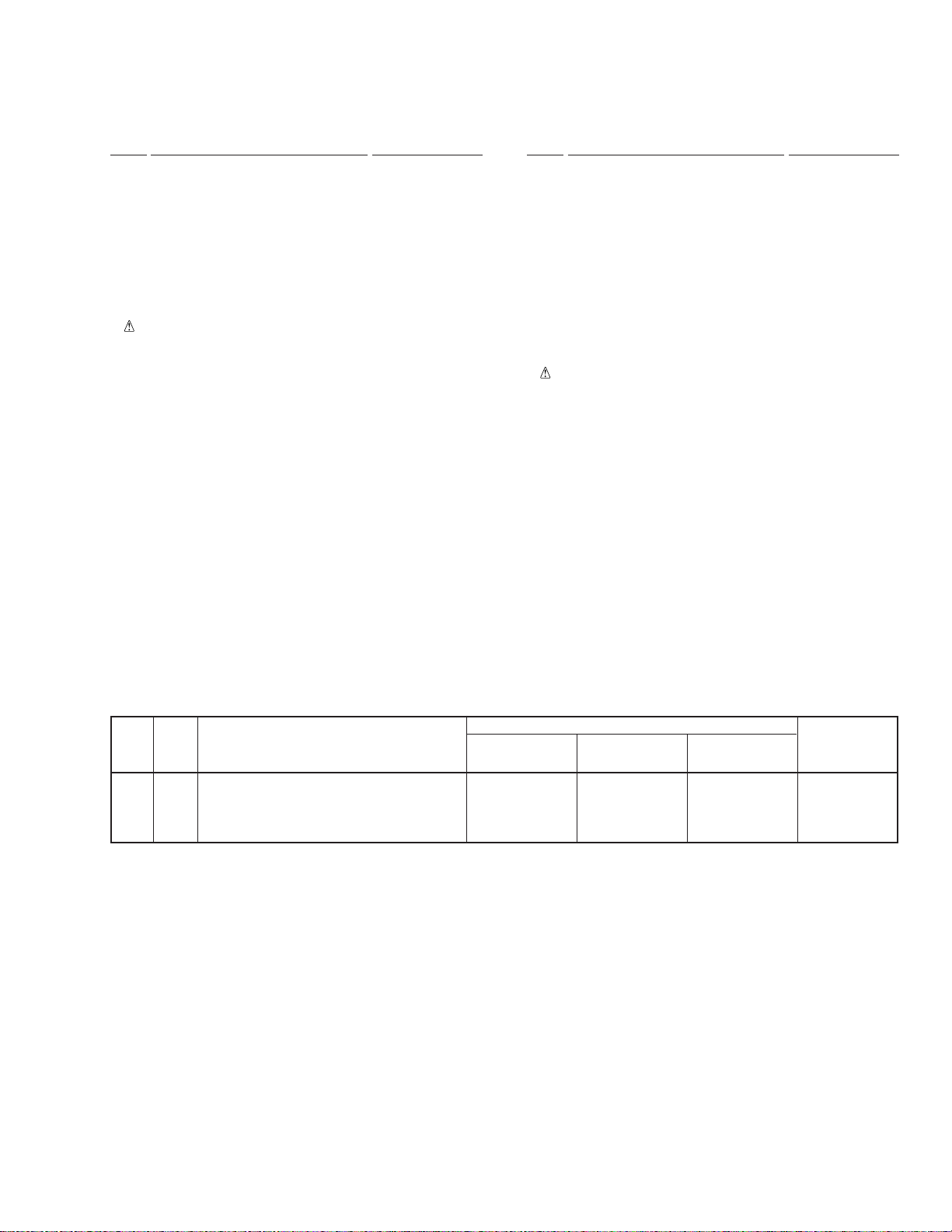
THIS MANUAL IS APPLICABLE TO THE FOLLOWING MODEL(S) AND TYPE(S).
Type
WY
WY/RD
WY/RE
Model
DV-717
Power Requirement
AC220 – 240V
AC220 – 240V
AC220 – 240V
Region restriction code
(region number)
2
4
5
ORDER NO.
RRV2010
Remarks
• Refer to the service guide RRV2004 for DV-515.
CONTENTS
1. SAFETY INFORMATION
......................................
2. EXPLODED VIEWS AND PARTS LIST
3. SCHEMATIC DIAGRAM
4. PCB CONNECTION DIAGRAM
5. PCB PARTS LIST
6. ADJUSTMENT
....................................................
.....................................
..........................
...............................................
................
10
33
45
50
2
3
7. GENERAL INFORMATION
7.1 PARTS
7.1.1 IC
7.2 DISASSEMBLY
.........................................................
...........................................................
...........................................
7.3 BLOCK DIAGRAM
7.4 CIRCUIT DESCRIPTION
7.4.1 VIDEO SIGNAL PROCESSING BLOCK..62
8. PANEL FACILITIES AND SPECIFICATIONS
................................
.......................................
............................
....
56
56
56
59
60
62
63
PIONEER ELECTRONIC CORPORATION 4-1, Meguro 1-Chome, Meguro-ku, Tokyo 153-8654, Japan
PIONEER ELECTRONICS SERVICE, INC. P.O. Box 1760, Long Beach, CA 90801-1760, U.S.A.
PIONEER ELECTRONIC (EUROPE) N.V. Haven 1087, Keetberglaan 1, 9120 Melsele, Belgium
PIONEER ELECTRONICS ASIACENTRE PTE. LTD. 501 Orchard Road, #10-00 Wheelock Place, Singapore 238880
PIONEER ELECTRONIC CORPORATION 1998
T – ZZM OCT. 1998 Printed in Japan
Page 2
DV-717
1. SAFETY INFORMATION
This service manual is intended for qualified service technicians ; it is not meant for the casual do-ityourselfer. Qualified technicians have the necessary test equipment and tools, and have been trained
to properly and safely repair complex products such as those covered by this manual.
Improperly performed repairs can adversely affect the safety and reliability of the product and may
void the warranty. If you are not qualified to perform the repair of this product properly and safely, you
should not risk trying to do so and refer the repair to a qualified service technician.
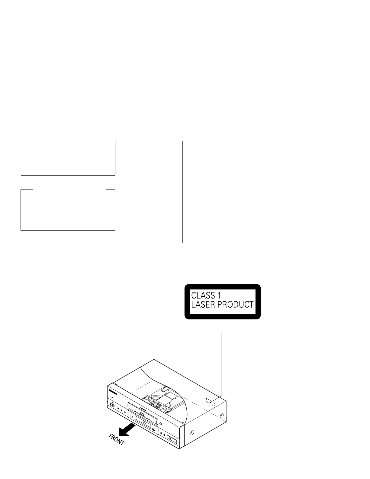
IMPORTANT
THIS PIONNER APPARATUS CONTAINS
LASER OF CLASS 1.
SERVICING OPERATION OF THE APPARATUS
SHOULD BE DONE BY A SPECIALLY
INSTRUCTED PERSON.
LASER DIODE CHARACTERISTICS
•FOR DVD
MAXIMUM OUTPUT POWER : 7 mW
WAVELENGTH : 650 nm
•FOR CD
MAXIMUM OUTPUT POWER : 5 mW
WAVELENGTH : 780-785 nm
LABEL CHECK
Additional Laser Caution
1. Inside detection switch (S201 on the SMEB assy) and loadingstatus detection switch (S301 on the LOSB assy) are detected
by the microprocessor (IC501 in the DVDM assy).
• To permit the laser diode to oscillate, it is required to set the
inside detection switch for the inside position (S201 : ON) and to
set the loading-status detection switch for the clamp position (the
center terminal of S301 is shorted to +5V). The 650 nm laser
diode for DVD oscillation will continue if pin 19 of IC101 is shorted
to +5V (fault condition) in the DVDM assy.
The 780 nm laser diode for CD oscillates if pin 20 of IC101 is
shorted to +5V in the DVDM assy.
In the test mode ∗ , the laser diode oscillates when microprocessor detects a PLAY signal, or when the PLAY key is pressed
(S113 ON in the FLKB assy), with the above requirements satisfied.
2. When the cover is open, close viewing through the objective lens
with the naked eye will cause exposure to the laser beam.
∗ Refer to the service guide RRV2004.
(Printed on the Rear Panel)
2
Page 3
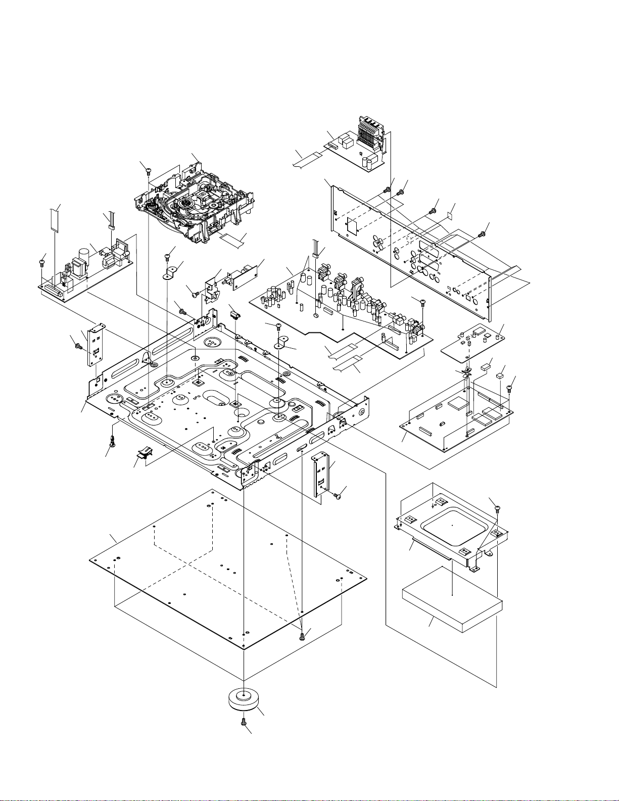
2. EXPLODED VIEWS AND PARTS LIST
NOTES:
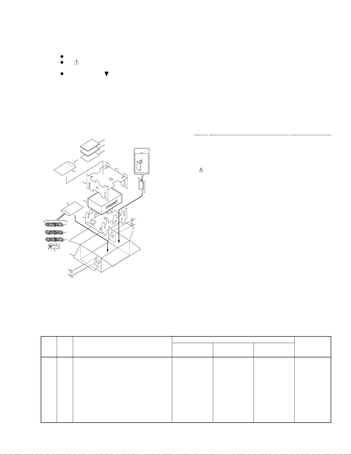
2.1 PACKING
Parts marked by "NSP" are generally unavailable because they are not in our Master Spare Parts List.
The mark found on some component parts indicates the importance of the safety factor of the part.
Therefore, when replacing, be sure to use parts of identical designation.
Screws adjacent to mark on product are used for disassembly.
(1) PACKING PARTS LIST
Mark No. Description Part No.
1 Instruction Manual VRE1074
(English/French/German/Italian)
2 Instruction Manual VRF1045
(Spanish/Portuguese/Dutch/Swedish)
NSP 3 Warranty Card ARY7022
NSP 7 Battery(R6P,AA) VEM-013
4 Power Cord ADG1127
5 Audio Cord (L=1.5m) VDE1033
6 Video Cord (L=1.5m) VDE1048
8 Remote Control Unit VXX2601
(CU-DV025)
9 Battery Cover VNK4334
10 Polyethylene Bag Z21-038
11 Protector A VHB1065
12 Protector B VHB1066
13 Packing Case VHG1779
14 Mirror Mat Sheet VHL1012
15 Region Label See contrast table (2)
16 Label See contrast table (2)
10
11
10
14
12
4
5
6
7
13
15
16
(Except WY Type)
1
2 (WY Type Only)
3 (Except
WY/RD
Type)
15
16 (Except
WY Type)
8
9
DV-717
(2) CONTRAST TABLE
WY, WY/RD and WY/RE types are constructed the same except for the following :
Part No.
Mark
No.
Symbol and Description Remarks
WY
type
2 Instruction Manual VRF1045 Not used Not used
(Spanish/Portuguese/Dutch/Swedish)
NSP 3 Warranty Card ARY7022 Not used ARY7022
15 Region Label P2 VRW1701 Not used Not used
15 Region Label P4 Not used VRW1705 Not used
15 Region Label P5 Not used Not used VRW1755
16 RD Label Not used VRW1761 Not used
16 RE Label Not used Not used VRW1756
WY/RD
type
WY/RE
type
3
Page 4
DV-717
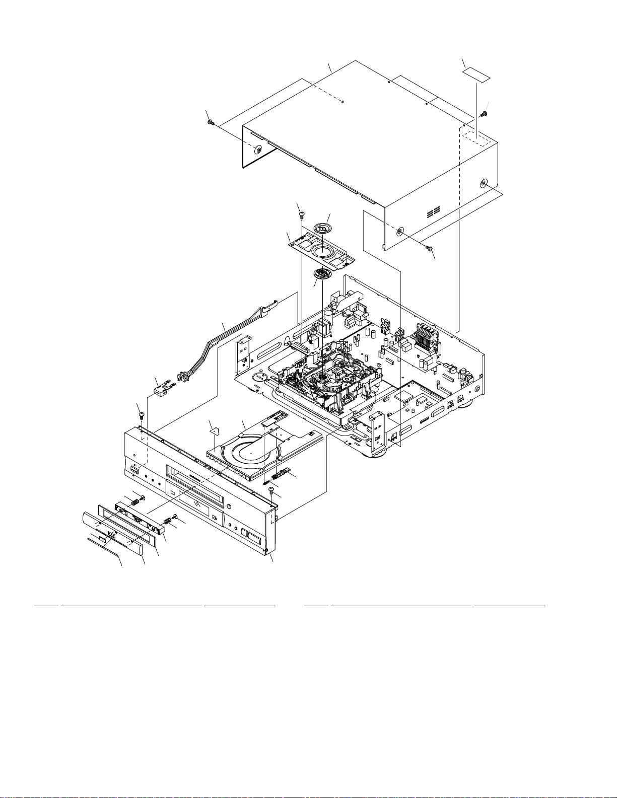
2.2 EXTERIOR SECTION
17
21
13
18
12
15
20
16
14
17
22
19
10
7
6
7
2
3
1
6
5
4
11
(1) EXTERIOR SECTION PARTS LIST
Mark No. Description Part No.
1 Door Plate VAH1312
2 DVD Plate VAM1077
3 Door Panel VNK4324
4 Door Cushion VEC2008
5 Door Holder VNK4325
9
8
19
Refer to "2.3 FRONT PANEL SECTION"
Mark No. Description Part No.
11 Tray VNK4333
12 Clamper VNL1738
13 Bridge VNE2069
14 Clamper Plate VNE2068
15 Bonnet Case S VXX2617
6 Door Spring VBH1305
7 Screw VBA1057
8 Spring VBH1277
9 Tray Stopper VNL1739
10 Label VRW1628
16 Screw BBZ30P080FMC
17 Screw BCZ40P060FNI
18 Screw BPZ26P080FZK
19 Screw BBT30P080FCC
20 Label VRW1699
21 PW Joint VNK4327
22 Power Button VNK4159
4
Page 5
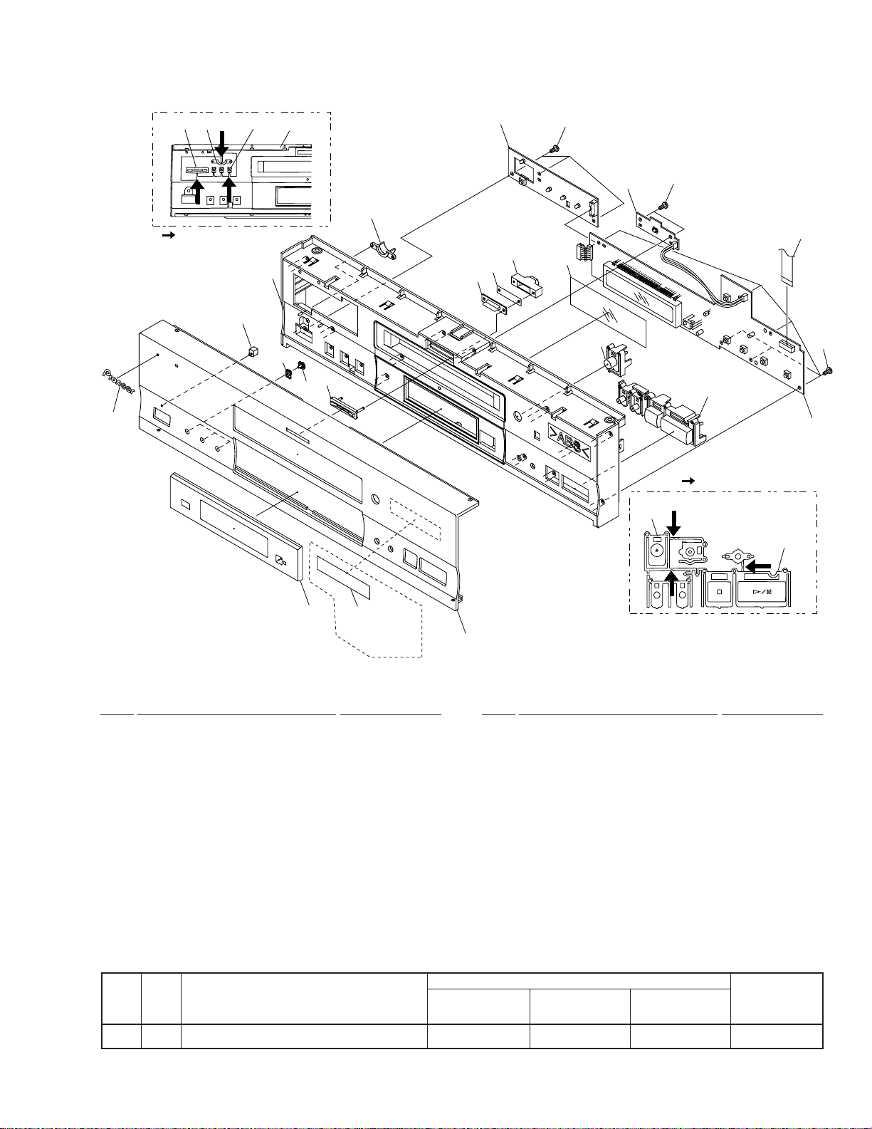
2.3 FRONT PANEL SECTION
DV-717
7(4/4)
:Cut position
3
7(3/4) 7(1/4)7(2/4)
7(1/4)
4
7(3/4)
7(4/4)
5
7(2/4)
15
11
10
9
12
17
8(2/2)
14
17
16
17
8(1/2)
13
:Cut position
8(2/2)
1
6
WY/RD
Type Only
2
(1) FRONT PANEL SECTION PARTS LIST
Mark No. Description Part No.
1 FL Lens VEC2007
2 Front Almi VAH1298
3 Name Plate G PAN1377
4 LED Lens PNW2019
5 LED Lens VNK4326
NSP 6 Getter See contrast table (2)
7 Panel Base VNK4323
8 Main Key VNK4095
9 Illumination Lens VNK4168
10 Illumination Filter VEC1950
Mark No. Description Part No.
11 Illumi Holder VNK4098
12 FL Filter VEC2016
13 FLKY Assy VWG1980
NSP 14 DIRB Assy VWG1991
NSP 15 PWSB Assy VWG1988
16 Flexible Cable VDA1690
17 Screw BBZ30P080FMC
(2) CONTRAST TABLE
WY, WY/RD and WY/RE types are constructed the same except for the following :
Part No.
Mark
No.
Symbol and Description Remarks
WY
type
NSP 6 Getter Not used VRW1757 Not used
WY/RD
type
WY/RE
type
8(1/2)
5
Page 6
DV-717
2.4 BOTTOM SECTION
20
25
20
Refer to
"2.5 LOADING MECHANISM ASSY"
20
20
33
18
26
7
8
9
19
32
10
6
3
20
11
31
12
30
17
29
28
7
27
21
20
21
21
34 (Except WY Type)
21
22
24
23
13
20
4
5
2
1
20
6
20
20
14
20
15
16
6
Page 7
(1) BOTTOM SECTION PARTS LIST
Mark No. Description Part No.
1 Insulator PNW2766
NSP 2 Bottom Plate PNA2376
NSP 3 Chassis VNA1979
NSP 4 PCB Holder PNW2029
5 Flat Cable Clip VEC2018
DV-717
Mark No. Description Part No.
21 Screw BBZ30P080FMC
NSP 22 PC Support Cushion VEC2033
NSP 23 PC Support Spacer VEC2032
24 PC Support DEC1932
25 Flexible Cable (26p) VDA1688
NSP 6 Panel Stay VNE2156
NSP 7 PCB Base RNE1221
NSP 8 Power-Holder VNE2123
NSP 9 P.Plate Holder PNY-405
10 Power Supply Unit VWR1306
NSP 11 MSWB Assy VWG1996
12 A VJB Assy VWV1617
13 DNRB Assy VWV1619
14 DVDM Assy VWS1349
NSP 15 Mecha Holder VNE2157
16 Mecha Cushion VEC2011
17 Rear Panel See contrast table (2)
NSP 18 Loading Mecha. Assy VWT1157
19 Screw BBZ30P100FMC
20 Screw ABZ30P080FCC
26 Flexible Cable (12p) VDA1692
27 Flexible Cable (26p) VDA1694
28 Flexible Cable (22p) VDA1696
29 Connector Assy PF02PP-S20
30 SCRB Assy VWV1623
31 Flexible Cable (22p) VDA1699
32 Housing Assy VKP2194
33 Screw PMB30P080FZK
34 Region Label See contrast table (2)
(2) CONTRAST TABLE
WY, WY/RD and WY/RE types are constructed the same except for the following :
Part No.
Mark
No.
Symbol and Description
WY
type
17 Rear Panel VNA1996 VNA2043 VNA2043
34 Region Label R4 Not used VRW1704 Not used
34 Region Label R5 Not used Not used VRW1754
WY/RD
type
WY/RE
type
Remarks
7
Page 8
DV-717
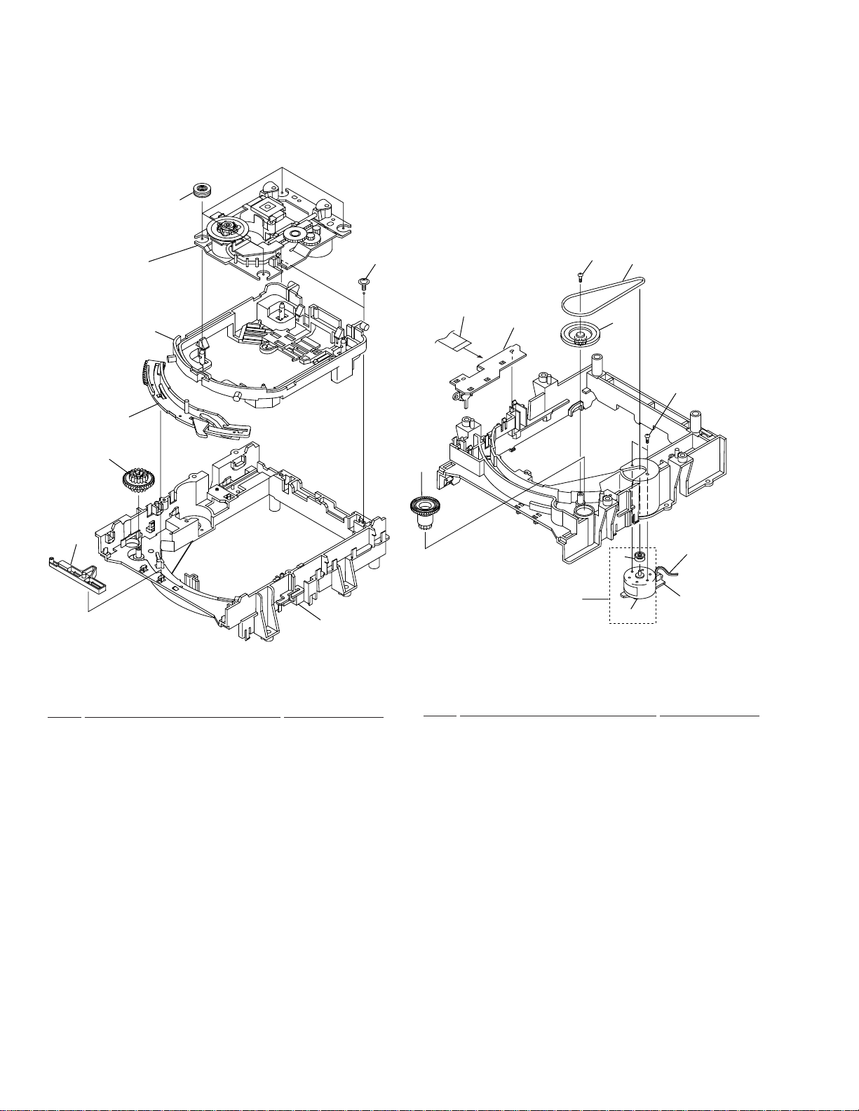
2.5 LOADING MECHANISM ASSY
• Top View • Bottom View
20
Refer to
"2.6 SERVO MECHANISM
ASSY"
5
1
19
3
4
2
18
10
6
9
17
11
13
7
8
16
15
14
12
LOADING MECHANISM ASSY PARTS LIST
Mark No. Description Part No.
1 Servo Mechanism Assy-S VXX2606
2 Screw DBA1006
3 Drive Cam VNL1736
4 Drive Gear VNL1735
5 Lock Plate VNL1820
6 Loading Base VNL1730
7 Belt VEB1260
8 Gear Pulley VNL1733
NSP 9 LOSB Assy VWG1885
10 Loading Gear VNL1734
8
Mark No. Description Part No.
11 Loading Motor Assy VXX2505
12 DC Motor / 0.3W PXM1027
13 Motor Pulley PNW1634
NSP 14 LOMB Assy VWG1886
15 Connector Assy VKP2184
(LOMB CN401 – LOSB CN306)
16 Screw VBA1055
17 Screw Z39-019
18 Flexible Cable (08P) VDA1698
(LOSB CN303 – SMEB CN202)
19 Float Base VNL1815
20 Floating Rubber VEB1286
Page 9
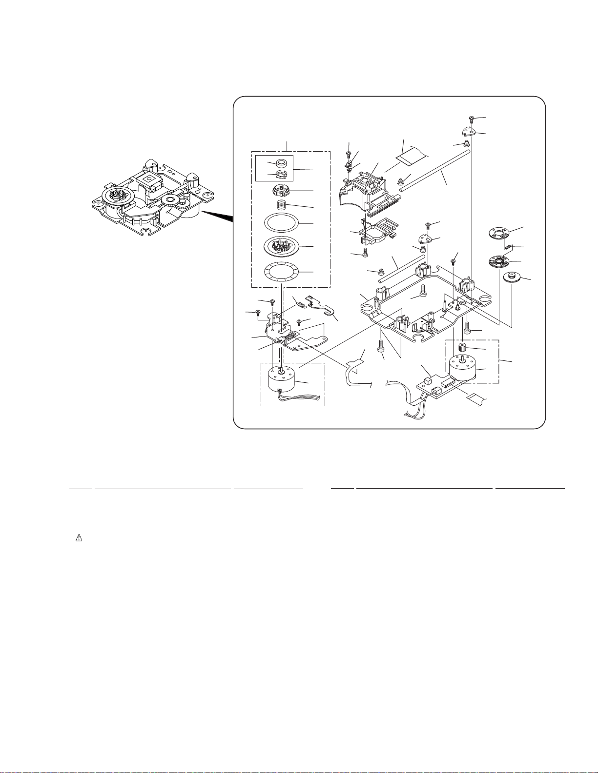
2.6 SERVO MECHANISM ASSY
• Top View
DV-717
37
37
17
31
24
30
16
35
33
28
34
19
8
6
20
12
9
37
4
15
22
33
10
23
21
2
38
10
5
10
13
37
10
14
7
7
18
32
1
18
26
11
25
27
7
29
36
3
SERVO MECHANISM ASSY PARTS LIST
Mark No. Description Part No.
NSP 1 SMEB Assy VWG1968
NSP 2 FGSB Assy VWG2009
3 Motor VXM1074
4 Motor VXM1075
5 Pickup Assy VWY1050
6 Table Sheet DEC2040
7 Screw VBA1058
8 Centering Spring VBH1278
9 Hook Spring VBH1291
10 Skew Spring VBH1303
11 Gear Spring VBH1308
NSP 12 Reflected Sheet VEC1959
13 Guide Bar VLL1504
14 Sub-guide Bar VLL1505
15 Hold Spring VNC1017
NSP 16 Magnet Holder VNE2070
NSP 17 Motor Base VNE2154
NSP 18 Cover VNE2155
19 Centering Ring VNL1746
NSP 20 Disc Table VNL1747
Mark No. Description Part No.
21 Hook VNL1770
22 FFC Holder VNL1802
23 Mechanism Base VNL1806
24 FG Holder VNL1807
25 Gear A VNL1808
26 Gear B VNL1809
27 Gear C VNL1810
28 Slider VNL1811
29 Gear D VNL1814
NSP 30 Magnet VYM1024
31 Screw JFZ17P025FZK
32 Screw JGZ17P028FMC
33 Screw VBA1051
34 Magnet Holder Assy VXX2507
35 Spindle Motor Assy VXX2604
36 Carriage Motor Assy VXX2605
37 Screw PBA1069
38 Flexible Cable (24P) VDA1701
(DVDM CN120 – Pickup Assy)
9
Page 10
1
23
DV-717
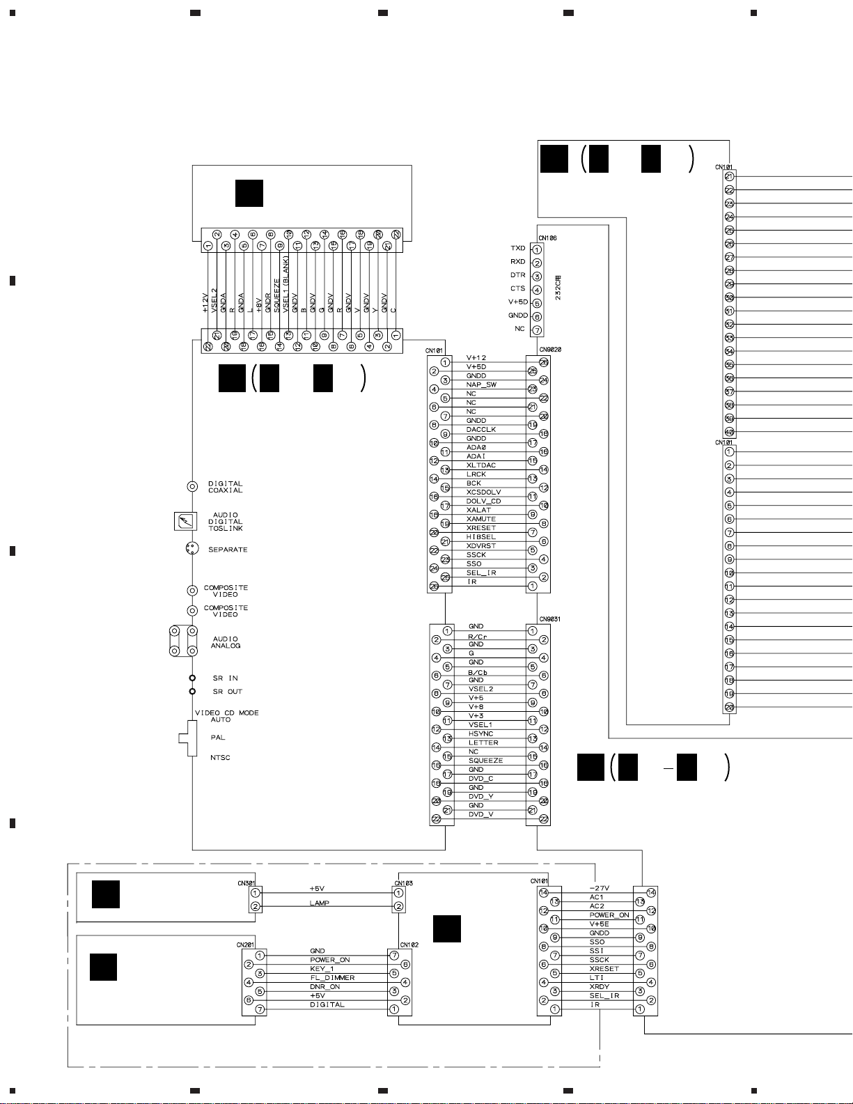
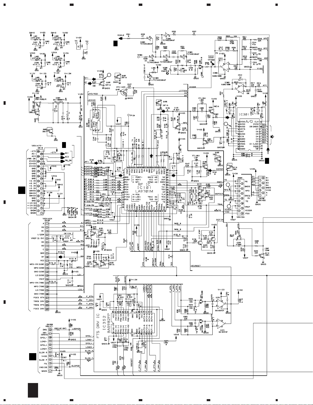
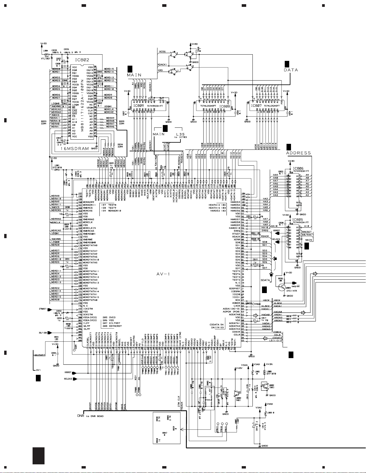
3. SCHEMATIC DIAGRAM
3.1 OVERALL CONNECTION DIAGRAM, LOMB,
A
LOSB, SMEB and FGSB ASSEMBLIES
SCRB ASSY
K
(VWV1623)
I
I I
1/2, 2/2
CN1001
CN103
J
J J
1/2, 2/2
DNRB ASSY
(VWV1619)
4
B
C
AVJB ASSY (VWV1617)
CN102
H
H H
1/3 3/3
DVDM ASSY
(VWS1349)
DILB ASSY
G
(VWG1991)
CN602
E
D
F PWSB ASSY
(VWG1988)
FLKB ASSY
(VWM1860)
10
1234
FLKY ASSY
(VWG1980)
Page 11
5
678
DV-717
Note : When ordering service parts, be sure to refer to "EXPLODED VIEWS and P AR TS LIST" or "PCB PARTS LIST".
L
MSWB ASSY
(VWG1996)
M
POWER
SUPPLY
ASSY
(VWR1306)
A
B
CN301
(F)
(F)
(T)
(F)
(T)
(T)
(F)
(S)
(S)
LOSB ASSY
B
(VWG1885)
PICKUP ASSY
(VWY1050)
CN302
(S)
(S)
CN303
B2B-PH-K-S
: RF SIGNAL ROUTE
(F)
: FOCUS SERVO LOOP LINE
(T)
: TRACKING SERVO LOOP LINE
(S)
: SLIDER SERVO LOOP LINE
FGSB ASSY
D
(VWG2009)
R101
680
(S)
(S)
CARRIAGE MOTOR ASSY
VXX2605
C
SMEB ASSY
(VWG1968)
C
CN401
LOMB ASSY
A
(VWG1886)
5
6
B2B-PH-K-S
LOADING
MOTOR
ASSY
:VXX2505
SPINDLE MOTOR ASSY
7
VXX2604
CBA
D
8
11
D
Page 12
1
23
DV-717
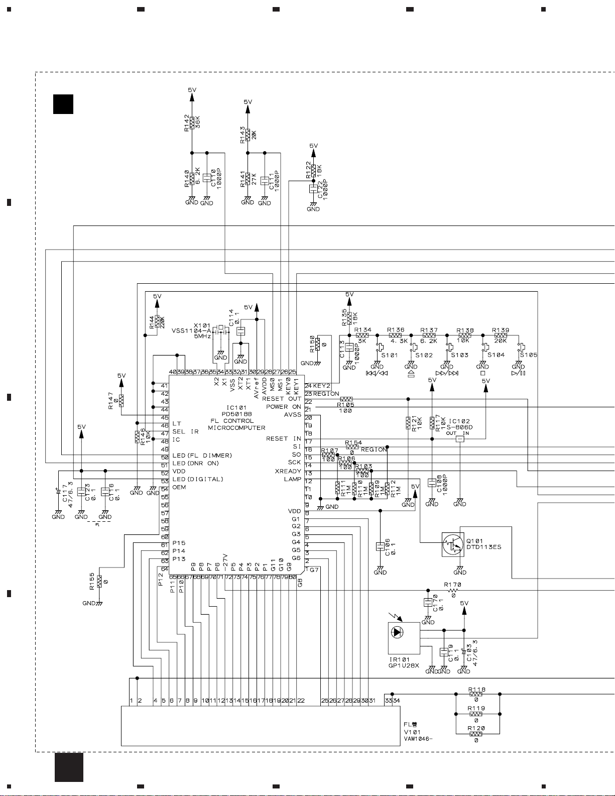
3.2 FLKY, PWSB and DILB ASSEMBLIES
4
A
E
FLKY ASSY
(VWG1980)
B
C
D
12
E
1234
Page 13
5
678
DV-717
PWSB ASSY
F
(VWG1988)
A
B
2/3
H
CN602
G
DILB ASSY
(VWG1991)
SWITCHES:
FLKY ASSY
S101: 4/1
S102: 0
S103: ¡/¢
S104: 7
S105: 6
FLKB ASSY
(VWM1860)
C
D
FE
5
6
7
G
8
13
Page 14
1
DV-717
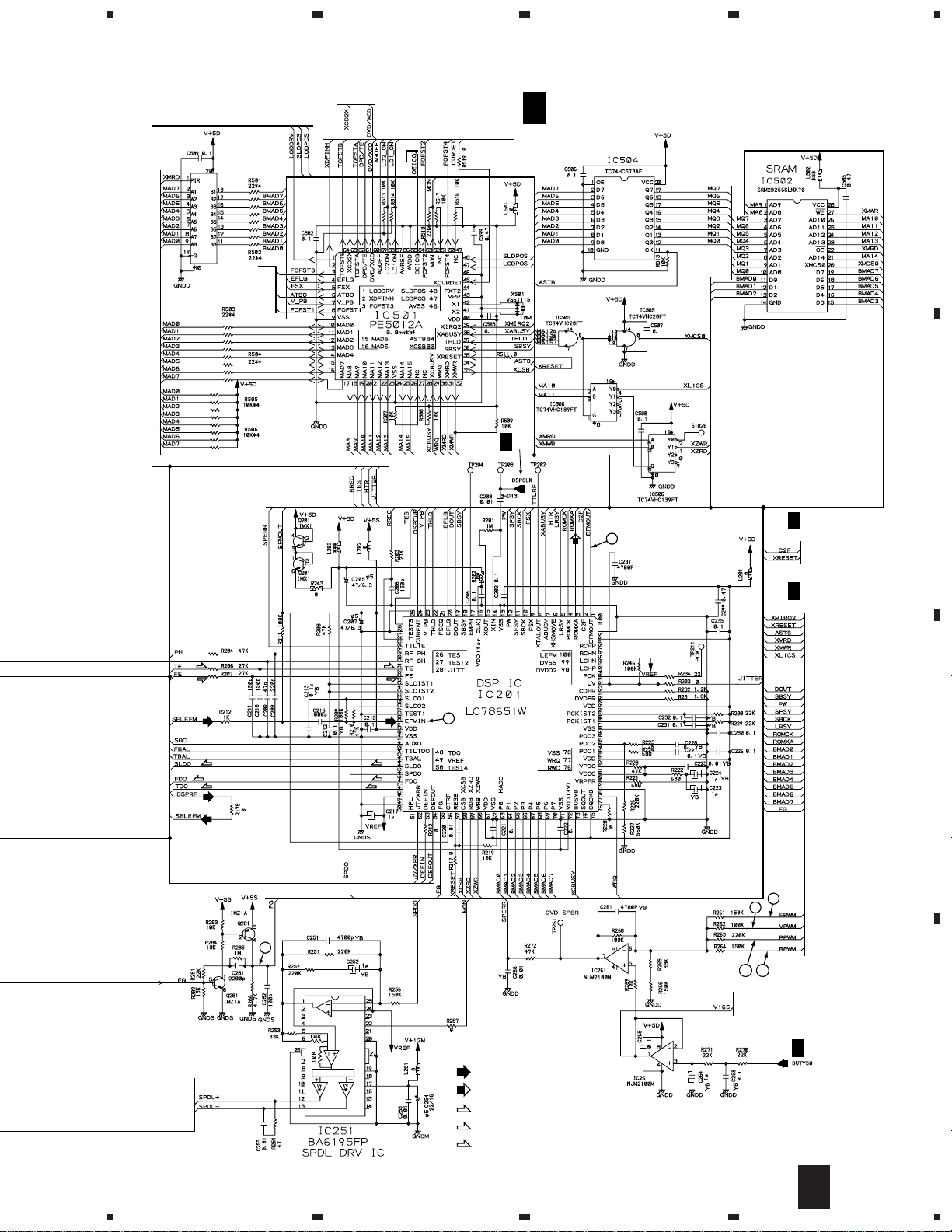
3.3 DVDM ASSY (1/3)
23
4
(4/6)
(DVD)
(1/6)
(5/6)
(CD)
(6/6)
1/2
from IC261
2/2
ADC1175CIJMX
(DVD)
3
(DVD)
(DVD)
to IC701
H
2/3
(CD)
(F)
(F)
to CN120
2
H
2/3
(2/6)
A
(3/6)
1
to IC501
to IC501
H
2/3
B
(DVD)
(F)
CN103
M
(T)
(T)
(F)
(F)
to
IC501
(F)
(F)
(T)
(T)
4
(T)
C
to IC501
PICKUP ASSY
(F)
(T)
(T)
(F)
D
CN301
B
(S)
(S)
(S)
(S)
2/2
1/2
(T)
(T)
(F)
(F)
(F)
(T)
14
1/3
H
1234
Page 15
5
678
DV-717
IC507
TC74VHCT245AFT
to IC101
from Q107,Q108
to CN120
to IC101
H
1/3
DVDM ASSY(1/3) (VWS1349)
A
1/2 2/2
(1/2)
H
3/3
B
(2/2)
H
2/3
6
(CD)
to IC601
(T)
(F)
(CD)
(CD)
H
2/3
to IC701
(T)
(F)
(CD)
(S)
(F)
(T)
(CD)
7
(S)
(F)
(T)
5
C
8
9
2/2
1110
to IC302
H
1/2
LEVEL SHIFT
5
6
: RF SIGNAL ROUTE
: ROM DATA SIGNAL ROUTE
(F)
: FOCUS SERVO LOOP LINE
(T)
: TRACKING SERVO LOOP LINE
(S)
: SLIDER SERVO LOOP LINE
7
2/3
H
1/3
8
D
15
Page 16
1
DV-717
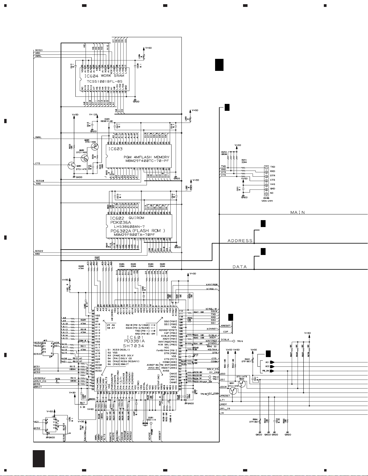
3.4 DVDM ASSY (2/3)
23
4
A
H
2/3
DVDM ASSY(2/3)
(VWS1349)
H
3/3
XCSDOLV,XCS6,XWRL,XWRH,XLT3,
XAMUTE,XDACK1,XDREQ1,IR,SEL-IR,
48/44,XDVRST1,XAVIRQ0,NSP-SW,
SSCK,SSO,XRESET
VYW1518
B
H
3/3
ADDRESS
A2–A10
H
3/3
DATA
C
H
1/3
IC605(1/2)
TC74VHC139FT
H
1/3
IC605(2/2)
TC74VHC139FT
D
16
2/3
H
1234
Page 17
5
: AUDIO SIGNAL ROUTE
: ROM DATA SIGNAL ROUTE
(DVD)
H
3/3
SDATA
(DVD)
678
DV-717
A
B
from IC701
H
3/3
from IC801
TC74VHCT541AFT
H
3/3
IC703
(DVD)
H
1/3
H
1/3
from IC301
H
3/3
(DVD)
MONITOR OUTPUT
H
1/3
from IC301
H
1/3
C
SERVO
H
1/3
H
to IC801
H
3/3
H
3/3
(CD)
1/3
H
3/3
H
1/3
E
CN101
to IC801
H
3/3
5
from IC201
H
6
1/3
H
1/3
2/3
H
7
8
17
D
Page 18
1
DV-717
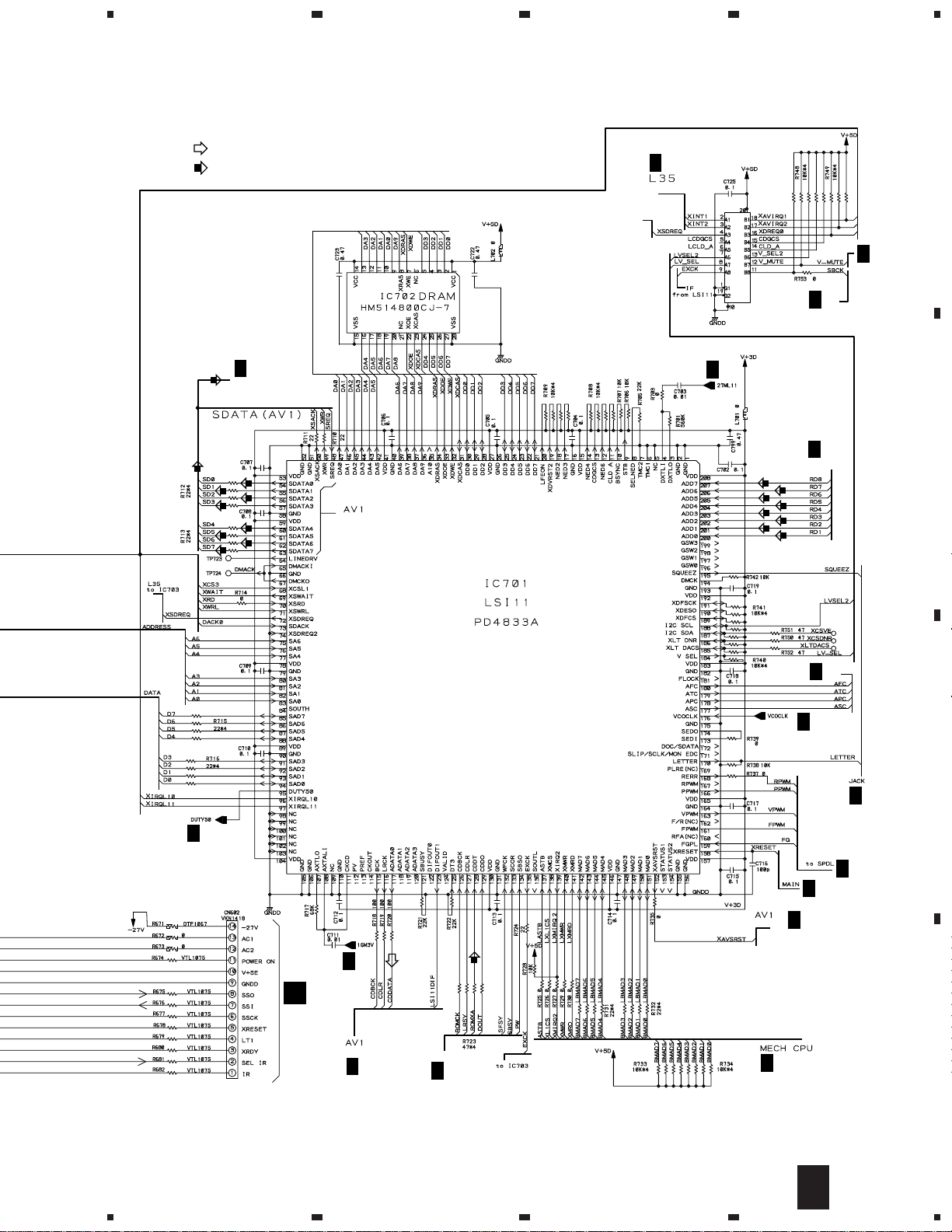
3.5 DVDM ASSY (3/3)
A
B
23
IC810(1/4)
TC74VHC00FT
IC810(2/4)
TC74VHC00FT
H
2/3
IC810(4/4)
TC74VHC00FT
H
2/3
IC810(3/4)
TC74VHC00FT
4
H
2/3
H
2/3
H
2/3
(DVD)
from IC701
H
2/3
(DVD)
from IC701
H
2/3
IC801
MB86371C
C
from IC701
H
2/3
D
18
3/3
H
1234
Page 19
5
678
DV-717
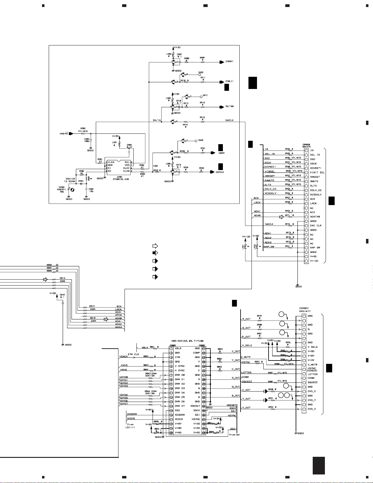
CLOCK GENERATOR SECTION
IC906(1/3)
IC906 :
TC7W04F
IC906(2/3)
IC904(1/3)
IC904(2/3)
IC904 :
TC7W04F
IC904(3/3)
: AUDIO SIGNAL ROUTE
: ROM DATA SIGNAL ROUTE
(V/CB)
: V/CB SIGNAL ROUTE
(Y)
: Y SIGNAL ROUTE
(C)
: C SIGNAL ROUTE
IC906(3/3)
H
for IC701
H
for IC201
for IC801
H
2/3
for IC801
2/3
1/3
H
H
3/3
DVDM ASSY(3/3)
(VWS1349)
2/3
A
1
2
3
4
5
6
7
8
9
10
11
12
13
14
15
16
17
18
19
20
21
22
23
24
25
26
1/2
I
CN101
B
H
2/3
17
18
15
14
(C)
(Y)
1613
1
2
R
3
4
5
6
B
7
8
9
10
11
12
13
14
15
16
17
18
19
20
21
22
2/2
I
CN102
C
D
3/3
H
5
6
7
8
19
Page 20
DV-717
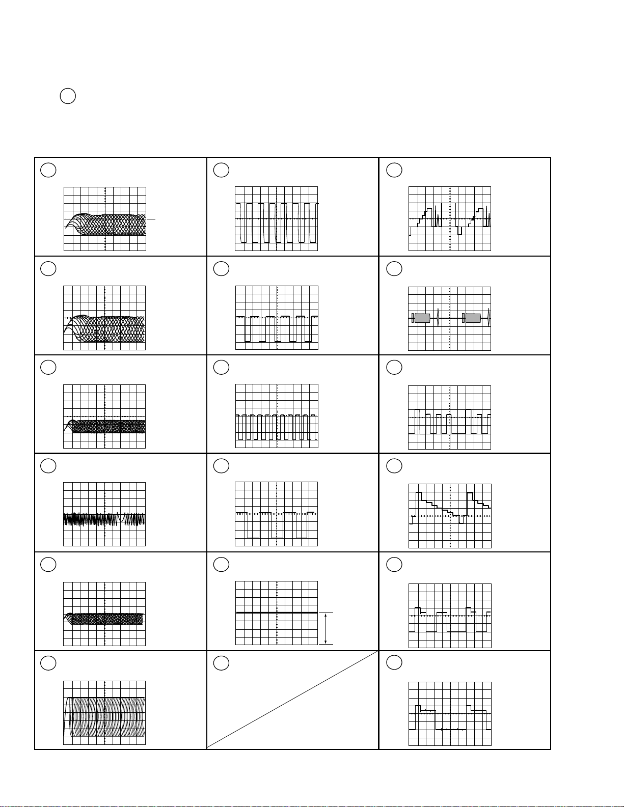
• WAVEFORMS OF DVDM ASSY
Note : No. in the table correspond to the number on the schematic diagram.
Measurement condition : No. 1 to 4 and 6 to 11 : Disc MJK1, Title 1-chp 1
Q109-Emitter (RF)
1
V: 100mV/div. H: 0.1µS/div.
TP (RFO)
2
V: 500mV/div. H: 0.1µS/div.
IC301-pin 19 (RF for A/D converter)
3
V: 1V/div. H: 0.2µS/div.
No. 5 : CD, ABEX-784 Track 1
No. 13 to 14 : MJK1, Title 1-chp 4
No. 15 to 18 : MJK1, Title 1-chp 5
Q281-Collector (FG)
7
V: 1V/div. H: 5mS/div.
DC 2V
Foot of R261 (FPWM)
8
V: 1V/div. H: 10µS/div.
Foot of R262 (VPWM)
9
V: 1V/div. H: 10µS/div.
CN9031-pin 20 (Y output)
13
V: 500mV/div. H: 10µS/div.
CN9031-pin 18 (C output)
14
V: 500mV/div. H: 10µS/div.
CN9031-pin 6 (B output when
15
selecting color difference output)
V: 500mV/div. H: 10µS/div.
TP (Tracking Error)
4
V: 1V/div. H: 2mS/div.
IC201-pin 39 (EFM before slice)
5
V: 1V/div. H: 1µS/div.
IC201-pin 1 (EFM)
6
V: 1V/div. H: 0.2µS/div.
Foot of R263 (PPWM)
10
V: 1V/div. H: 0.2µS/div.
Foot of R264 (RPWM)
11
12
DC1.4V
CN9031-pin 20 (Y output when
16
selecting color difference output)
V: 500mV/div. H: 10µS/div.
CN9031-pin 2 (R output when
17
selecting color difference output)
V: 500mV/div. H: 10µS/div.
CN9031-pin 4 (G output when
18
selecting color difference output)
V: 500mV/div. H: 10µS/div.
20
Page 21

DV-717
21
Page 22

1
DV-717
3.6 AVJB ASSY (1/2)
A
3/3
H
CN9020
B
23
I
2/2
I
2/2
4
C
D
22
1/2
I
1234
Page 23

5
678
DV-717
: AUDIO SIGNAL ROUTE
I
1/2
AVJB ASSY(1/2)
(VWV1617)
A
B
C
D
1/2
I
5
6
7
8
23
Page 24

1
DV-717
3.7 AVJB ASSY (2/2)
A
I
1/2
I
1/2
B
23
I
2/2
AVJB ASSY(2/2)
(VWV1617)
4
C
3/3
H
CN9031
680
680
D
24
2/2
I
1234
Page 25

(V/CB)
: V/CB SIGNAL ROUTE
(Y)
: Y SIGNAL ROUTE
(C)
: C SIGNAL ROUTE
5
678
DV-717
A
K
CN1001
B
C
D
2/2
I
5
6
7
8
25
Page 26

1
DV-717
3.8 DNRB ASSY (1/2)
A
B
23
4
CONNECTOR
(Y)
C
D
(C)
(B)
(G)
(R)
26
1/2
J
1234
Page 27

5
678
DV-717
(R)
: R SIGNAL ROUTE
J
1/2
DNRB ASSY(1/2)
(VWV1619)
(G)
: G SIGNAL ROUTE
(B)
: B SIGNAL ROUTE
(Y)
: Y SIGNAL ROUTE
(C)
: C SIGNAL ROUTE
J
2/2
A
B
C
D
1/2
J
5
6
7
8
27
Page 28

1
DV-717
3.9 DNRB ASSY (2/2)
A
J
B
1/2
23
J
2/2
DNRB ASSY(2/2)
(VWV1619)
4
B LEVEL
ADJ.
G LEVEL
ADJ.
C
(Y)
Y LEVEL
ADJ.
(C)
D
C LEVEL
ADJ.
28
2/2
J
1234
Page 29

5
678
DV-717
(R)
: R SIGNAL ROUTE
(G)
: G SIGNAL ROUTE
(B)
: B SIGNAL ROUTE
(Y)
: Y SIGNAL ROUTE
(C)
: C SIGNAL ROUTE
A
(G)
(B)
(B)
(G)
B
(R)
R LEVEL
ADJ.
C
(Y)
(Y)
(Y)
(C)
(C)
(Y)
(C)
(C)
D
2/2
J
5
6
7
8
29
Page 30

1
DV-717
3.10 SCRB ASSY
A
2/2
I
CN103
B
K
SCRB ASSY (VWV1623)
23
4
C
D
30
K
1234
Page 31

5
678
DV-717
A
UPPER
B
BELLOW
C
D
K
5
6
7
8
31
Page 32

1
23
DV-717
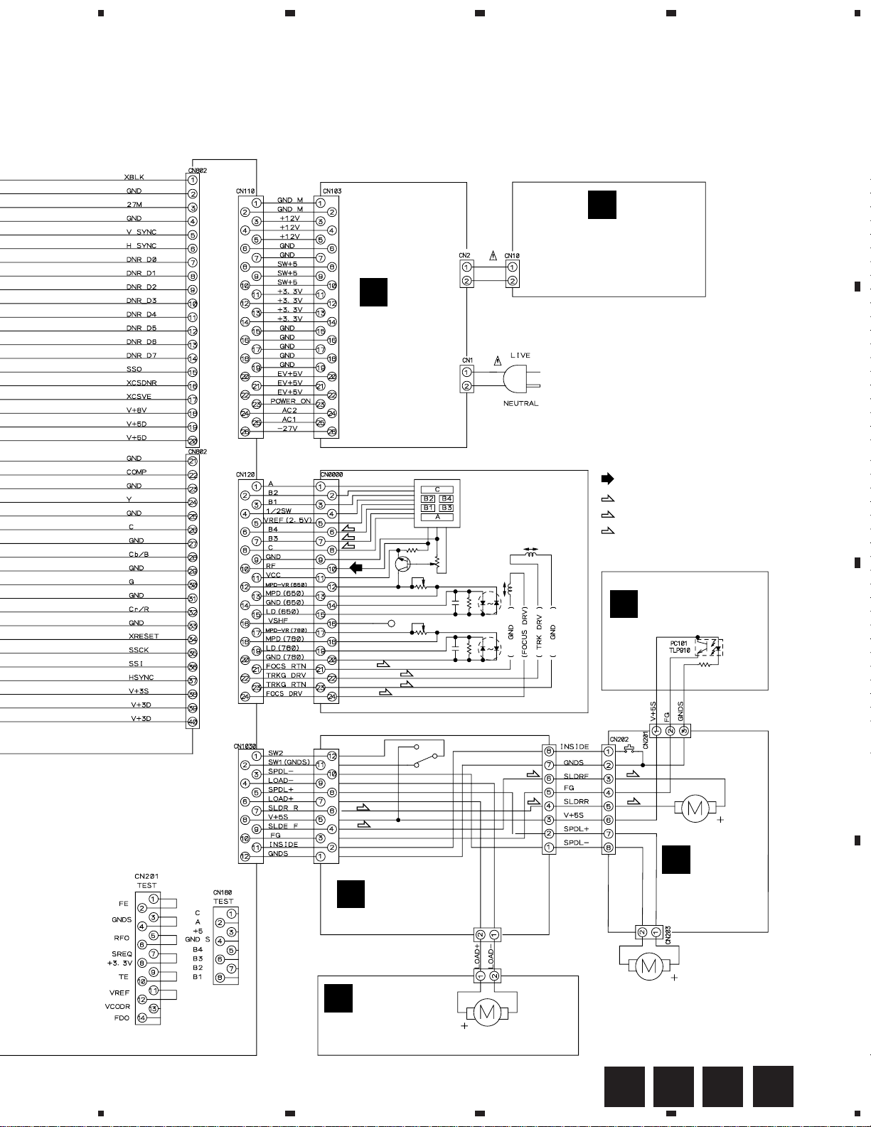
3.11 POWER SUPPLY ASSY and MSWB ASSY
A
H
1/3
4
CN110
1A
B
800mA
1.6A
800mA
C
POWER
L
MSWB ASSY
0.01/AC250V
D
POWER SUUPLY ASSY (VWR1306)
2.5A
(VWG1996)
M
AC POWER
CORD
32
L
N
L M
1234
Page 33

1
234
4. PCB CONNECTION DIAGRAM
DV-717
NOTE FOR PCB DIAGRAMS :
1. Part numbers in PCB diagrams match those in the schematic
diagrams.
2. A comparison between the main parts of PCB and schematic
diagrams is shown below.
Symbol In PCB
Diagrams
BCE
BCE
D
Symbol In Schematic
Diagrams
BCEBCE
BCE
DGGSS
BCE
DGS
Part Name
Transistor
Transistor
with resistor
Field effect
transistor
Resistor array
3-terminal
regulator
3. The parts mounted on this PCB include all necessary parts for
several destinations.
For further information for respective destinations, be sure to
check with the schematic diagram.
4. View point of PCB diagrams.
Connector
Capacitor
SIDE A
P.C.Board
Chip Part
SIDE B
A
B
4.1 LOMB, LOSB, SMEB and FGSB ASSEMBLIES
LOSB ASSY
B
(VNP1628-A)
CN1030
H
SPINDLE
MOTOR
M
(VNP1654-A)
SMEB ASSY
C
PC101
R101
LOMB ASSY
A
(VNP1628-A)
FGSB ASSY
D
LOADING
MOTOR
(VNP1661-B)
C
D
SIDE A
BA
1
2
3
C
D
4
33
Page 34

1
23
DV-717
4.2 FLKY, PWSB and DIRB ASSEMBLIES
4
A
B
PWSB ASSY
F
IC102
DIRB ASSY
G
FLKY ASSY
E
C
D
34
E
F G
1234
Page 35

5
678
DV-717
FLKY ASSY
E
DIRB ASSY
G
CN602
H
SIDE A
A
B
IC102 Q101
PWSB ASSY
F
(VNP1656-B)
SIDE B
C
Q201Q202Q203
IC101 Q102
5
6
D
(VNP1656-B)
E
7
F G
8
35
Page 36

1
DV-717
4.3 DVDM ASSY
23
4
A
B
J
CN101
PICKUP
ASSY
DVDM ASSY
H
• This PCB is a four-layered board. Middle layer is mainly connected to Vcc and GND.
CN102
I
CN101
I
VC901
VR801
Q604
IC881
Q881
IC904
Q914
IC801
IC602
IC803
Q109
Q111
Q108
Q107 Q105 IC703
Q603
IC804 Q801
Q802 IC603
IC702 IC604
IC203
Q106
Q662
Q661
C
VC301
IC101
Q113
Q103
B
CN301
D
CN103
J
CN101
E
(VNP1651-A)
IC352
Q402 Q403
IC251
IC301
IC261
IC302
IC303
IC401
Q401
IC507
IC501
SIDE A
36
H
1234
Page 37

5
678
DV-717
DVDM ASSY
H
• This PCB is a four-layered board. Middle layer is mainly connected to Vcc and GND.
Q601 Q602 IC906
Q872
Q862 Q852
IC901
IC605
Q871 Q861 Q851
IC601 IC806
IC805 Q803
IC903
IC810 IC807
IC809 IC808
IC802
A
B
(VNP1651-A)
IC701
IC201
Q114
Q301
Q102
IC506
IC504
IC502
Q201
Q112
C
Q101
IC505
IC371
Q281
Q251
D
SIDE B
H
5
6
7
8
37
Page 38

1
DV-717
4.4 AVJB ASSY
23
4
A
B
AVJB ASSY
I
C
CN1001
K
Q821IC402
IC821
D
38
I
1234
Q801
Q831
IC841
IC831
IC802
IC401
IC801
IC822
IC301 Q941Q753 Q772Q771
IC201IC202 IC102Q752
Page 39

5
678
DV-717
A
SIDE A
B
102
CN9031
H
Q721Q722Q711 IC601
CN9020
H
IC602
(VNP1658-A)
C
D
39
I
5
6
7
8
Page 40

A
Q
1
DV-717
AVJB ASSY
I
23
4
Q901 Q902
B
Q921IC604IC702
IC704
C
D
40
I
1234
Page 41

5
604 Q503
IC704
IC706
Q504Q922Q923Q921
678
Q802
Q832
Q803
Q833
IC501
IC602
DV-717
A
SIDE B
Q502Q501
B
D2002
D2001
C
(VNP1658-A)
D
41
I
5
6
7
8
Page 42

1
DV-717
23
4
4.5 DNRB ASSY
IC104 IC103
SIDE A
A
B
DNRB ASSY
J
(VNP1655-A)
CN802
H
SIDE B
C
DNRB ASSY
J
42
(VNP1655-A)
Q651Q652
Q602
Q601
Q611
Q612
Q621Q622
VR504VR505VR508 VR507 VR501-503
IC101
IC102
J
1234
D
Page 43

1
4.6 SCRB ASSY
234
DV-717
SCRB ASSY
K
Q1225
CN103
I
SIDE A
A
B
(VNP1658-A)
SCRB ASSY
K
Q1001
Q1201
Q1222
Q1202
Q1203
Q1205
Q1204
SIDE B
(VNP1658-A)
C
D
K
1
2
3
4
43
Page 44

1
23
DV-717
4.7 POWER SUPPLY and MSWB ASSEMBLIES
A
POWER SUPPLY ASSY
M
IC102
IC103
4
SIDE A
H
CN110
B
IC201
C
MSWB ASSY
L
VR
201
Q1
IC51
Q71
(VNP1658-A)
D
44
L M
1234
AC IN
Page 45

5. PCB PARTS LIST
NOTES:
Parts marked by "NSP" are generally unavailable because they are not in our Master Spare Parts List.
The mark found on some component parts indicates the importance of the safety factor of the part.
Therefore, when replacing, be sure to use parts of identical designation.
When ordering resistors, first convert resistance values into code form as shown in the following examples.
Ex.1 When there are 2 effective digits (any digit apart from 0), such as 560 ohm and 47k ohm (tolerance is shown by J=5%,
and K=10%).
560
47k
0.5
1
Ex.2 When there are 3 effective digits (such as in high precision metal film resistors).
5.62k RN1/4PC F562 x 10
56 x 10
47 x 103
R50
1R0
DV-717
1
561
473
1
5621
RD1/4PU J
RD1/4PU J
RN2H K
RS1P K
561
473
R50
1R0
5621
Mark No. Description Part No.
LIST OF WHOLE PCB ASSEMBLIES
NSP LOAB ASSY VWM1798
NSP LOMB ASSY VWG1886
NSP LOSB ASSY VWG1885
NSP SMEB ASSY VWG1968
NSP FGSB ASSY VWG2009
NSP FLKB ASSY VWM1860
FLKY ASSY VWG1980
NSP PWSB ASSY VWG1988
NSP DILB ASSY VWG1991
DVDM ASSY VWS1349
NSP JKSB ASSY VWM1863
AVJB ASSY VWV1617
SCRB ASSY VWV1623
NSP MSWB ASSY VWG1996
DNRB ASSY VWV1619
POWER SUPPLY ASSY VWR1306
LOMB ASSY
OTHERS
CN401 KR CONNECTOR B2B-PH-K-S
LOSB ASSY
SWITCH
S301 VSK1011
OTHERS
CN303 KR CONNECTOR B2B-PH-K-S
CN302 8P FFC CONNECTOR VKN1268
CN301 12P FFC CONNECTOR VKN1272
SMEB ASSY
SWITCH
S201 DSG1016
Mark No. Description Part No.
OTHERS
CN201 3P FFC CONNECTOR 52044-0345
CN202 8P FFC CONNECTOR VKN1212
PC BOARD(SMEB) VNP1654
FGSB ASSY
SEMICONDUCTOR
PC101 TLP910(O)
RESISTORS
All Resistors RS1/10S&&&J
FLKB ASSY
OTHERS
PC BOARD(FLKB) VNP1656
FLKY ASSY
SEMICONDUCTORS
IC101 PE5018B
IC102 S-806D
Q101 DTD113ES
Q102 PDTA124EK
D102 EP05Q04
SWITCHES AND RELAYS
S101–S105 RSG1030
CAPACITORS
C101, C103, C117 CEJA470M6R3
C108, C110–C113 CKSQYB102K50
C106, C107, C114–C116, C119 CKSQYF104Z25
C123, C170 CKSQYF104Z25
RESISTORS
All Resistors RS1/10S&&&J
45
Page 46

DV-717
Mark No. Description Part No.
OTHERS
CN102 CONNECTOR 7P 07P-FJ
REMOTE RECEIVER UNIT GP1U28X
J101 CONNECTOR ASSY PF02NN2D12
V101 FL TUBE VAW1046
SPACER VEC1599
CN101 14P CONNECTOR VKN1274
HOLDER VNF1087
X101 CERAMIC RESONA TOR (5MHz) VSS1104
PWSB ASSY
SEMICONDUCTORS
Q201 PDTC124EK
D201–D204 SLP9118C51H
CAPACITORS
C201 CKSQYF104Z25
RESISTORS
All Resistors RS1/10S&&&J
OTHERS
CN201 CONNECTOR 7P 07R-FJ
Mark No. Description Part No.
IC504 TC74HC573AF
IC303 TC74HCU04AF
IC807, IC808 TC74LCX245FT
IC810 TC74VHC00FT
IC506, IC605 TC74VHC139FT
IC505 TC74VHC20FT
IC805, IC806, IC809 TC74VHC541FT
IC507 TC74VHCT245AFT
IC703 TC74VHCT541AFT
IC903, IC904, IC906 TC7WU04F
IC603 VYW1599
Q401 2SB1260
Q603 DTA114EK
Q107, Q602 DTC114EK
Q601, Q661, Q662, Q803 DTC114TK
Q108 HN1K03FU
Q102, Q106, Q109 IMT1A
Q101, Q105, Q112–Q114, Q201 IMX1
Q402 IMX1
Q103, Q281, Q301 IMZ1A
D301 KV1410
D371, D372 MA152WK
D601 RB501V-40
DILB ASSY
SEMICONDUCTORS
D301 MA111
OTHERS
PL301 LAMP VEL1022
DVDM ASSY
SEMICONDUCTORS
IC301 ADC1175CIJMX
IC371 BA10393F
I
C401 BA178M08FP
IC352 BA5982FP
IC251 BA6195FP
IC901 CY2081SL-638
IC702 HM514800CJ-7
IC101 LA9701M
IC201 LC78651W
IC802 MB811 171622A-100FN
IC801 MB86371C
IC261, IC302 NJM2100M
IC601 PD3381A
IC701 PD4833A
IC602 PDK036A
IC501 PE5012A
IC502 SRM2B256SLMX70
IC604 TC551001BFL-85
COILS AND FILTERS
F6630, F6640, F6710 CHIP BEADS DTF1067
F4010, F4020, F4030 CHIP BEADS DTF1070
F4040, F4050, F4060 CHIP BEADS DTF1070
F8010, F8050, F8900 CHIP BEADS DTF1070
F8920, F8990 CHIP BEADS DTF1070
F8450, F8460 FERRITE BEADS VTF1073
L304 (1.5mH) VTL1059
L101, L303 (10mH) VTL1061
L804 (22µH) VTL1067
L6740, L6750, L6760 CHIP BEADS VTL1075
L6770, L6780, L6790 CHIP BEADS VTL1075
L6800, L6810, L6820 CHIP BEADS VTL1075
L9050, L9580, L9590 CHIP BEADS VTL1075
L9620, L9630, L9870 CHIP BEADS VTL1075
L9880, L9890, L9960 CHIP BEADS VTL1075
L8420 CHIP BEADS VTL1108
CAPACITORS
C605 CCSRCH100D50
C123, C282, C610, C611, C716 CCSRCH101J50
C903 CCSRCH101J50
C206, C210, C211, C240 CCSRCH151J50
C126, C307, C905 CCSRCH180J50
C116 CCSRCH220J50
C152, C208 CCSRCH221J50
C135 CCSRCH270J50
C322 CCSRCH330J50
C352, C360 CCSRCH331J50
C104–C108, C124, C209, C314 CCSRCH470J50
46
Page 47

DV-717
Mark No. Description Part No.
C324 CCSRCH470J50
C117, C122 CCSRCH471J50
C128, C309 CCSRCH560J50
C127, C308 CCSRCH5R0C50
C134 CCSRCH680J50
C145, C146 CCSRCH820J50
C129, C142, C414, C832 CEV101M10
C113, C139, C254, C358, C409 CEV220M16
C411 CEV220M16
C801, C802, C811, C814, C836 CEV221M4
C111, C147, C149, C205, C207 CEV470M6R3
C301, C304, C368, C401, C403 CEV470M6R3
C405, C407, C807, C812, C815 CEV470M6R3
C140, C223, C224, C252, C264 CKSQYB105K10
C312, C803, C804, C813, C817 CKSQYB105K10
C819, C821, C823, C826 CKSQYB105K10
C829–C831, C833 CKSQYB105K10
C217, C302, C305, C417 CKSQYF105Z16
C216, C313, C323 CKSRYB102K50
C133, C136, C203, C220, C225 CKSRYB103K50
C253, C255, C266, C320, C321 CKSRYB103K50
C616, C662, C703, C711 CKSRYB103K50
C101, C102, C114, C118, C121 CKSRYB104K16
C130, C138, C153, C204 CKSRYB104K16
C212, C213, C227, C228 CKSRYB104K16
C231, C232, C263, C311 CKSRYB104K16
C315–C317, C362–C365, C413 CKSRYB104K16
C805, C806, C808, C810 CKSRYB104K16
C281 CKSRYB222K50
C137, C354, C357 CKSRYB223K25
C237, C239, C251, C261 CKSRYB472K50
C109, C110, C120, C131, C143 CKSRYF104Z16
C148, C150, C202, C215 CKSRYF104Z16
C221, C222, C226, C230, C235 CKSRYF104Z16
C265, C303, C306, C319, C359 CKSRYF104Z16
C366, C367, C369–C372, C402 CKSRYF104Z16
C404, C406, C408, C410, C412 CKSRYF104Z16
C415, C502, C503, C506–C509 CKSRYF104Z16
C603, C604, C606–C609 CKSRYF104Z16
C612–C615, C617–C620, C661 CKSRYF104Z16
C691, C702, C704–C710 CKSRYF104Z16
C712–C715, C717–C719, C725 CKSRYF104Z16
C818, C820, C822, C824, C825 CKSRYF104Z16
C827, C828, C834, C838, C840 CKSRYF104Z16
Mark No. Description Part No.
R607–R611, R723 (47Ω) DCN1090
R505, R506, R615, R616, R620 (10kΩ) DCN1094
R692, R708, R709, R733, R734 (10kΩ) DCN1094
R740, R741, R748, R749 (10kΩ) DCN1094
R121, R501–R504, R603–R606 (22Ω) DCN1104
R691, R712, R713, R715, R716 (22Ω) DCN1104
R731, R732, R816, R818, R819 (22Ω) DCN1104
R833–R835 (22Ω) DCN1104
R1020, R162, R173, R2010, R2020 RS1/10S0R0J
R243, R2510, R301, R3010, R302 RS1/10S0R0J
R3020, R3050, R3510, R3520 RS1/10S0R0J
R405–R407, R5010, R5020, R6010 RS1/10S0R0J
R6020, R6030, R6040, R672, R673 RS1/10S0R0J
R7010, R7020, R8020, R8030, R839 RS1/10S0R0J
R891, R9010, R9020, R9030, R9040 RS1/10S0R0J
R9510, R9520, R982–R984 RS1/10S0R0J
R202 RS1/10S101J
R807 RS1/16S1500F
R164 RS1/16S5600F
Other Resistors RS1/16S&&&J
OTHERS
FLEXIBLE CABLE(07P) VDA1681
CN106 7P CONNECTOR VKN1299
CN201 CONNECTOR VKN1324
CN602 14P CONNECTOR VKN1418
CN120 24P CONNECTOR VKN1464
CN1030 12P CONNECTOR VKN1471
CN9031 22P CONNECTOR VKN1477
CN110, CN9020 26P CONNECTOR VKN1479
CN180 CONNECTOR VKN1485
CN802 CONNECTOR VKN1529
LABEL VRW1750
X601 CERAMIC RESONAT OR(20MHz) VSS1114
X501 CERAMIC RESONAT OR(10MHz) VSS1115
X901 CRYSTAL RESONA T OR VSS1129
(13.824MHz)
JKSB ASSY
OTHERS
PC BOARD(JKSB) VNP1658
C842, C843, C845, C847, C907 CKSRYF104Z16
C910, C915 CKSRYF104Z16
C816, C837, C844, C848 (2.2µF/6.3V) VCG1030
C299, C328, C505, C599 (0.47µF/10V) VCG1032
C602, C722, C723, C799, C902 VCG1032
VC301 (40pF) VCM1010
VC901 (30pF) VCM1011
RESISTORS
R123 (39Ω) ACN7047
A VJB ASSY
SEMICONDUCTORS
IC821 IR3M03AN
IC702, IC704, IC706 MC14577CF
IC501, IC502 NJM5532MD
IC841 NJM78L05A
IC802 NJM78M05FA
IC801, IC831 NJM78M08FA
IC822 NJM79M05FA
47
Page 48

DV-717
Mark No. Description Part No.
IC812 NJM79M08FA
IC301 PD0236AM
IC201 PD2058A
IC401, IC402 PE8001A
IC202 TC4W53F
IC102 TC74HCT7007AF
IC601 TC74HCU04AF
IC602 TC7SET08F
IC604 TC7WU04F
Q502 2PB709A
Q751–Q753, Q802, Q832 2PD601A
Q901, Q902 2PD601A
Q801, Q821, Q831 2SB1566
Q503, Q504 2SD2114K
Q941 PDTA124EK
Q501, Q851 PDTC124EK
Q771, Q772 UMD2N
Q711, Q721, Q722 UMZ1N
D821 EC10QS04
D2001, D2002, D801, D802, D831 EP10QY03
D841 EP10QY03
D503 MA111
COILS AND FILTERS
F2001, F2002 CHIP BEADS DTF1070
L564, L565 CHIP INPEDER DTL1028
L2004 LAU2R2J
L2001–L2003, L823 LFA101J
L813, L821, L822 LFA470J
L101 COIL PTL1003
L602 COIL RTF1167
F121, F122, F301, F401–F404 VTF1096
F411–F414, F601, F603, F676 VTF1096
L824 (47µH) VTL1118
L2005–L2007 CHIP BEADS VTL1096
SWITCHES AND RELAYS
S101 VSH1020
CAPACITORS
C853 CCSQCH101J50
C823 CCSQCH181J50
C656 CCSQCH220J50
C784, C785 CCSQCH300J50
C503, C523 CCSQCH330J50
Mark No. Description Part No.
C907 CEAT470M10
C404, C419, C817 CEAT470M16
C501, C511, C521, C531 CEAT471M10
C824, C825 CEAT471M16
C851 CEAT471M6R3
C505, C509, C525, C529 CEBA470M10
C819, C827, C829 CEHAQ101M10
C801–C803, C833, C842 CEHAQ2R2M50
C2001, C2003–C2006, C513, C533 CKSQYB102K50
C830 CKSQYB102K50
C422, C805, C831 CKSQYF103Z50
C102, C104, C2002, C201–C204 CKSQYF104Z25
C207, C2222, C302, C303 CKSQYF104Z25
C402, C403, C407, C412, C416 CKSQYF104Z25
C423, C426, C502, C512, C522 CKSQYF104Z25
C532, C602–C604, C607, C608 CKSQYF104Z25
C611, C612, C654, C655, C702 CKSQYF104Z25
C754, C757, C759, C761, C791 CKSQYF104Z25
C806–C809, C816, C818, C826 CKSQYF104Z25
C828, C832, C834, C841, C843 CKSQYF104Z25
C902, C904, C929 CKSQYF104Z25
C122, C2007, C405, C411, C418 CKSQYF105Z16
C421, C657 CKSQYF105Z16
C711, C713, C715 CKSQYF225Z16
C504, C524 CQHA221J2A
C821 CQMBA104J50
RESISTORS
R747 RN1/10SC68R0D
R746, R748, R749 RN1/10SC75R0D
R907 RN1/10SE1001D
R501, R520, R714 RN1/10SE1002D
R503, R522 RN1/10SE1003D
R508, R528 RN1/10SE1602D
R504, R506, R507, R523 RN1/10SE2200D
R525, R526 RN1/10SE2200D
R724, R725 RN1/10SE2201D
R509, R529 RN1/10SE2701D
R502, R521 RN1/10SE2702D
R717, R722, R768, R769 RN1/10SE4700D
R904, R952 RN1/10SE5601D
R711 RN1/10SE6200D
Other Resistors RS1/10S&&&J
C652, C653, C729–C732 CCSQCH470J50
C507, C508, C527, C528 CCSQCH681J50
C103, C205, C206, C301, C601 CEAT101M10
C606, C610, C701, C755, C760 CEAT101M10
C792–C795, C901, C903 CEAT101M10
C101, C822 CEAT101M16
C401, C410, C415, C420 CEAT102M6R3
C852 CEAT220M25
C658, C718 CEAT221M6R3
C712, C753, C758, C762, C763 CEAT470M10
48
OTHERS
604 2P RCA PINJACK AKB7076
CN110 CONNECTOR POST B2B-PH-K-S
SCREW BBZ30P080FCC
JA101 OPTICAL LINK OUT GP1F32T
JA605, JA606 JACK RKN1004
VEF1040
JA601 JACK VKB1074
JA501 JACK VKB1095
JA502 JACK VKB1096
JA607 JACK VKB1118
Page 49

DV-717
Mark No. Description Part No.
CN102, CN103 22P CONNECTOR VKN1253
CN101 26P CONNECTOR VKN1257
SCREW PLATE VNE1948
KN1–KN3 EARTH METAL FITTING VNF1084
X201 CERAMIC RESONAT OR(24MHz) VSS1118
DNRB ASSY
SEMICONDUCTORS
IC301 BA178M05FP
IC101 CXD1854Q
IC102 MC44724A
IC103 TC74HCT02AF
IC104 TC74HCT74AF
IC105 TC7WU04F
Q501, Q502, Q511, Q512 2PB709A
Q521, Q522, Q541, Q542 2PB709A
Q551, Q552, Q622 2PB709A
Q621 2PD601A
COILS AND FILTERS
F1102, F201, F202, F501 DTF1070
F101, F102 VTF1147
L9404, L9409 VTL1074
L621 VTL1113
Mark No. Description Part No.
SCRB ASSY
SEMICONDUCTORS
Q1204 2PB709A
Q1001, Q1201, Q1203, Q1205 2PD601A
Q1223 2SA933S
Q1202, Q1221, Q1222 PDTC124EK
D1002, D1004, D1223 MA111
D1221, D1222 UDZS5.1B
SWITCHES AND RELAYS
RY1001-RY1004 RSR1029
CAPACITORS
C1151, C1152, C1161, C1162 CCSQCH391J50
C1012 CEAT101M10
C1011 CEAT101M16
C1001–C1008, C1016, C1221 CKSQYF104Z25
C1401–C1405 CKSQYF104Z25
RESISTORS
R1105, R1106, R1110–R1112, R1208 RN1/10SC75R0D
R1171–R1175 RN1/10SE1801D
R1151, R1152, R1161, R1162 RN1/10SE2200D
Other Resistors RS1/10S&&&J
CAPACITORS
C402 CCSRCH101J50
C622 CCSRCH470J50
C106, C213, C302, C304, C307 CEV470M6R3
C301, C303, C305, C306, C404 CKSQYF104Z25
C102 CKSQYF105Z16
C101, C103–C105, C107, C201 CKSRYF104Z16
C203, C205, C207, C209, C212 CKSRYF104Z16
C214, C215, C217–C220, C401 CKSRYF104Z16
C403, C501, C502, C511, C512 CKSRYF104Z16
C521, C522, C541, C542 CKSRYF104Z16
C551, C552, C623 CKSRYF104Z16
RESISTORS
R133, R134, R311, R312 RA4C470J
R313, R314, R322, R9101 RS1/10S0R0J
R9401, R9402 RS1/10S0R0J
R217, R219 RS1/16S1001F
R214, R215 RS1/16S1801F
R216, R218 RS1/16S2201F
R505, R515, R525, R545, R555 RS1/16S5600F
VR501–VR503, VR505, VR506(220Ω) VCP1179
Other Resistors RS1/16S&&&J
OTHERS
CN101 CONNECTOR VKN1530
OTHERS
JA1001 CONNECTOR VKB1056
CN1001 22P CONNECTOR VKN1282
EARTH PLATE VNF1097
MSWB ASSY
SWITCHES AND RELAYS
S10 ASG1006
CAPACITORS
C10 ACG7010
OTHERS
CN10 CONNECTOR2P 2-178496-4
POWER SUPPLY ASSY
OTHERS
F1 FUSE (2.5A) REK1102
P101 PROTECTOR (1A) AEK7009
P103,P301 PROTECTOR AEK7008
P102 PROTECTOR (1.6A) AEK7012
(800mA)
49
Page 50

DV-717
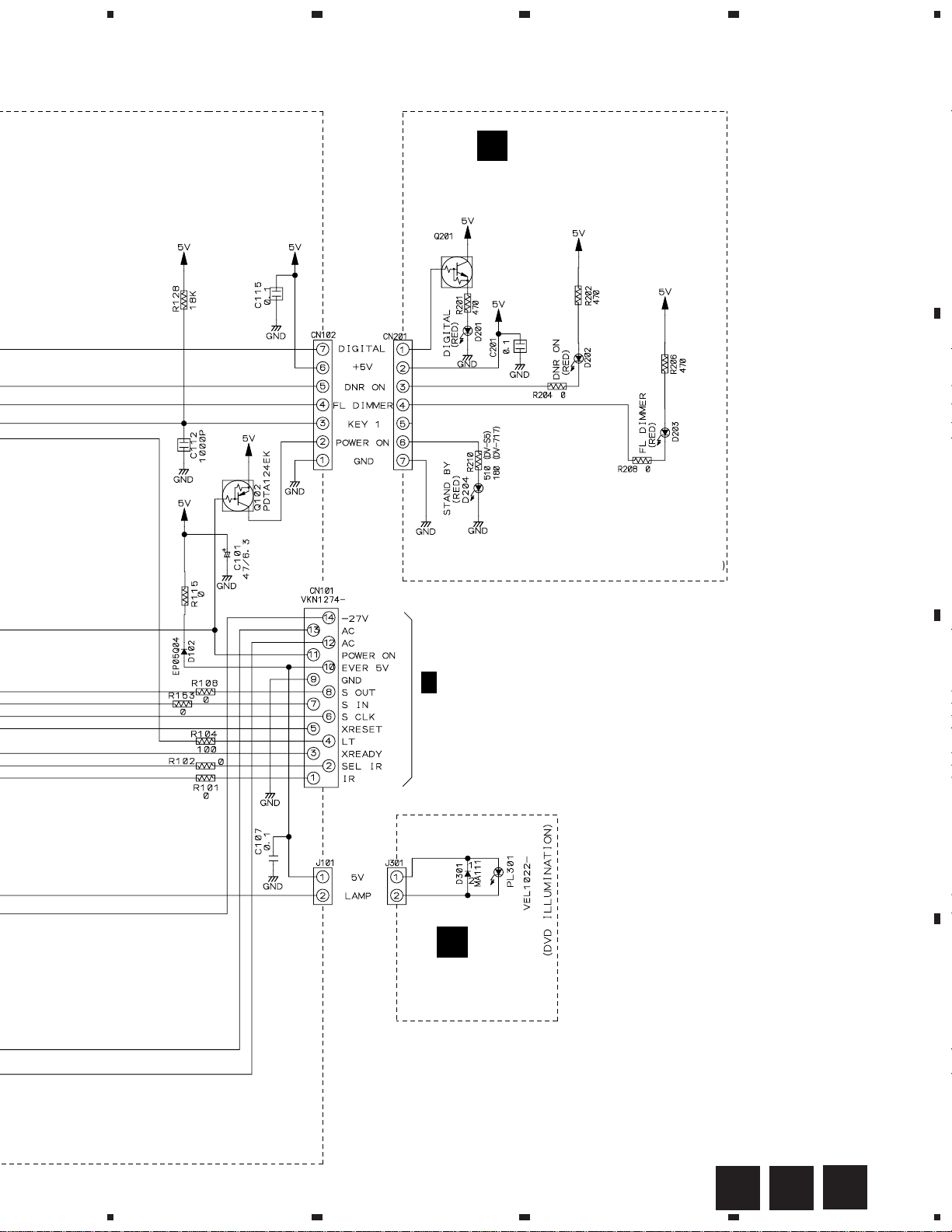
6. ADJUSTMENT
6.1 ADJUSTMENT ITEMS AND LOCATION
Adjustment Points (PCB Part)
DVDM ASSY
CN9020CN9031
1
1
IC801
MB86371C
VC901
CN201
1, 2 : Focus Error
3, 4 : GND
5, 6 : RF
7 : S REQ
8 : 3.3V
9,10 : Tracking Error
11,12 : VREF (Approx. 2.5V)
13 : VCO DR
14 : Focus Drive(DSP output)
14
13
CN201
CN110
2
1
IC302
2
VC301
IC904
5
CN120
CN1030
SIDE A
1
Adjustment Items
[Electrical Part]
1 16MHz Master Clock Adjustment
2 VCO Offset Adjustment
3 Y Level Adjustment
4 C Level Adjustment
5 R Level Adjustment
6 G Level Adjustment
7 B Level Adjustment
DNRB ASSY
SIDE B
1
5
6
3
7
4
How to output the VIDEO SIGNAL without the DNRB ASSY
a) When PC Board No. is VNP1651
1 Connect A1 and A2 with the wire jumper
DVDM ASSY
2 Connect B1 and B2 with the Resistor(150Ω)
b) When PC Board No. is VNP1684
1 Connect A1 and A2 with the wire jumper
A1
B1
B2
A2
50
Note:The PC Board was running-changed
from VNP1651 to VNP1684
2
Resistor
150Ω
1
Wire Jumper
location
A1:R991(CN9031 20pin)
A2:IC801 45pin
B1:R991
B2:L803(
Resistor 0Ω
)
Page 51

6.2 JIGS AND MEASURING INSTRUMENTS
DVD test disc (DVD-MJK1)
Frequency counter
Display digit 8-digit
Screwdriver(small)
TV monitor
Screwdriver(small)
DV-717
CH1 CH2
(X) (Y)
Dual-trace oscilloscope
(with delay)
Frequency band 40MHz
6.3 NECESSARY ADJUSTMENT POINTS
When
EXCHANGE PCB ASSY
Exchange board
AVJB ASSY
Exchange board
DVDM ASSY
Exchange board
DNRB ASSY
Mechanical
point
Electric
point
Mechanical
point
Electric
point
Note : 1 and 2 are adjusted already.
Mechanical
point
Adjustment Points
Electric
point
Note : 3 , 4 , 5 , 6 and 7 are adjusted already.
51
Page 52

DV-717
6.4 ELECTRICAL ADJUSTMENT
1
16MHz Master Clock Adjustment
• Normal mode
• Power ON
Player
START
DVDM ASSY
5
IC904
2
VCO Offset Adjustment
DVDM ASSY
16.934400MHz ± 80Hz
VC901
Frequency counter
52
• Normal mode
• Play the DVD test disc
START
DVDM ASSY
1
IC302
Player
VC301
DVDM ASSY
Probe (10:1)
CH1 CH2
(X) (Y)
1.9V± 0.1V
GND
Oscilloscope
V: 50mV/div.
H: 10msec/div.
DC mode
TV trigger
Page 53

3
Y Level Adjustment
DV-717
• Normal mode
• Play the DVD test disc
at the composite signal
part
Player (Rear)
START
TV monitor
VIDEO
IN
C Level Adjustment
4
VIDEO
OUT
DNRB
ASSY
VR505
Probe (10:1)
CH1 CH2
(X) (Y)
Oscilloscope
1Vp-p
V: 20mV/div.
H: 10µsec/div.
AC mode
• Normal mode
• Play the DVD test disc
at the composite signal
part
START
TV monitor
Player (Rear)
VIDEO
IN
VIDEO
OUT
DNRB
ASSY
VR506
Probe (10:1)
Burst
0.286Vp-p
CH1 CH2
(X) (Y)
Oscilloscope
V: 10mV/div.
H: 10µsec/div.
AC mode
53
Page 54

DV-717
5
R Level Adjustment
• Normal mode
• Play the DVD test disc
at the 100% color-bar
signal part
START
TV monitor
VIDEO
IN
6
G Level Adjustment
EURO CONNECTOR
R OUT
Player (Rear)
DNRB
ASSY
VR503
Probe (10:1)
CH1 CH2
(X) (Y)
Oscilloscope
0.7Vp-p
V: 20mV/div.
H: 10µsec/div.
AC mode
START
54
• Normal mode
• Play the DVD test disc
at the 100% color-bar
signal part
TV monitor
VIDEO
IN
EURO CONNECTOR
G OUT
Player (Rear)
DNRB
ASSY
VR502
Probe (10:1)
CH1 CH2
(X) (Y)
Oscilloscope
0.7Vp-p
V: 20mV/div.
H: 10µsec/div.
AC mode
Page 55

7
B Level Adjustment
DV-717
• Normal mode
• Play the DVD test disc
at the 100% color-bar
signal part
START
TV monitor
VIDEO
IN
EURO CONNECTOR
B OUT
Player (Rear)
DNRB
ASSY
VR501
Probe (10:1)
CH1 CH2
(X) (Y)
Oscilloscope
0.7Vp-p
V: 20mV/div.
H: 10µsec/div.
AC mode
55
Page 56

DV-717
7. GENERAL INFORMATION
7.1 PARTS
7.1.1 IC
• The information shown in the list is basic information and may not correspond exactly to that shown in the schematic diagrams.
List of IC
•
PE5018B, PE5012A, PD3381A
7
PE5018B (FLKY ASSY : IC101)
• FL Control IC
Pin Function
•
.oNkraMemaNniPO/InoitcnuF.oNkraMemaNniPO/InoitcnuF
149P7G
239P6G2413P13PIdesutoN
329P5G3403P)CN(O noitcennocnoN
419P4G4430P30PIdesutoN
509P3G5420PREWOPNOI
618P2G6410PTLI
708P1G7400PRILESI tupnilangislortnocetomeR
8DDVCCV − nipylppusrewoP84CICI − –
972P)CN(O noitcennocnoN9427P)CN(O noitcennocnoN
0162P)CN(O noitcennocnoN0517PDELFFOLFO NO:LFFO/NODELFFOLF
1152P)CN(O noitcennocnoN1507PDEL.S.D.VO
2142PPMALO NO:HFFO/NOpmalDVD25DDVDDV − nipylppusrewoP
3132PYDAERXO
4122PKCSO/I
5112POSO/I
6102PISI
71TESERNITESERI teseR:LtupniteseR75321P)CN(
8147P)CN(O noitcennocnoN85221P)CN(
9137P)CN(O noitcennocnoN95121P)CN(
02SSVASSV − DNG06021P)CN(
1271PNOREWOPO NO:HFFO/NOV5WS16711P51P
2261PTUOTESERO teseR:LtupnitesermetsyS26611P41P
3251P)CN(O noitcennocnoN36511P31P
4241P2NIK
5231P1NIK56311P11P
6221P0NIK66211P01P
7211P1SM
8201P0SM86011P8P
92DDVADDVA − nipylppusrewoP96701P7P
03FERVAFERVA − nipylppusrewopecnerefeR07601P6P
1340P40PIdesutoN17DAOLVV72– − V72–roftupnI
232TX)CN( − noitcennocnoN27501P5P
33SSVSSV − DNG37401P4P
431X1XI
532X2X − 57201P2P
6373P)CN(O noitcennocnoN67101P1P
7363P)CN(O noitcennocnoN77001P11G
8353P)CN(O noitcennocnoN8779P01G
9343P43PIdesutoN9769P9G
0433P33PIdesutoN0859P8G
ONO:HtuptuognimitLF
htiwenilekahsdnahnoitacinummoC
rellortnocmetsys
noissimrepnoitacinummoC:L
rellortnoc
rellortnoc
metsyshtiwtupniatadnoitacinummoC
rellortnoc
ItupniyeK
ItupninoitanimircsidnoitanitseD
kcolcrossecorporcimatcennoC
1423P23PIdesutoN
35721P)CN(
metsyshtiwtuptuokcolcnoitacinummoC
45621P)CN(
metsyshtiwtuptuoatadnoitacinummoC
55521P)CN(
65421P)CN(
46411P21P
76111P9P
47301P3P
rellortnocmetsys
)ylno515-VD(NO:L
OnoitcennocnoN
ONO:HtuptuotnemgesLF
ONO:HtuptuotnemgesLF
LFtaNOREWOP/YBTSehthctiwS
YBTS:Lp.udesirsirellortnoc
htiwenilekahsdnahnoitacinummoC
noissimrepnoitacinummoC:H
FO/NODELdnuorruSybloDlautriV
56
Page 57

PE5012A (DVDM ASSY : IC501)
• Mechanism Control IC
Pin Function
•
.oNemaNniPO/InoitcnuF.oNemaNniPO/InoitcnuF
1VRDDOLO/ItuptuoevirdrotomgnidaoL33BSCXO "L"tuptuognittesdnammoclellarapPSD
2HNIFDXO/I
33TSFOFO )dexifH(desutoN53TESERXI "L"tupnitesermetsyS
4GLFEI
5XSFI 73DLHTTNIDLOHT
6OBTAO/ItnemtsujdatesffognikcarT83YSUBAXTNI"L"tupniysubecneuqesotuaPSD
7BPVI
81TSFOFO/I1tnemtsujdatesffosucoF04DDV
9SSV
010DAM
111DAM34PPV
212DAM442TXP
313DAM54TEDRUCXI
414DAM64SSVA
515DAM74SOPDOLI tupniWSnoitisoppmalcgnidaoL
616DAM84SOPDLSI tupniWSnoitisopredilS
717DAM94WSROODIdesutoN
818AM
919AM15TSRPSDXOdesutoN
0201AM25NOMO "L"tuptuoNOrotomeldnipS
1211AM352TSFOFO/I2tnemtsujdatesffosucoF
2221AM45GCIEOO Bd6otpuniagCIEO:"H"
3231AM55DDVA
42SSV
5241AM
6251AM85NO2DLO langisNOedoidresalmn087
72)06P(OdesutoN95FFOGAO FFOotsnrutCIFRfoCGA:"H"
82DLXRDOdesutoN06DCX/DVDO DC:L,DVD:H
92YSUBCXI "L"elbissopsinoitpecerdnammocPSD16ETXDPDO
03QRWI QedocbusfogalfelbadaeR26ATSFOTO/IAtnemtsujdaecnalabgnikcarT
13DRMXO "L"eslupdaerUPC36X2DCXOdesutoN
23RWMXO "L"eslupetirwUPC46CTSFOTO/ICtnemtsujdaecnalabgnikcarT
DNG142X
−
O/IsubatadsserddalanretxE
OsubsserddalanretxE
DNG65FERVAI retrevnocD/AroftupniegatlovecnerefeR
−
OsubsserddalanretxE
FFOTCEFEDtatuptuo"L"
etarrorrefotupniatadtnuoC
langiskcolovresMFE
NOTCEFEDta)tupni(ecnadepmihgiH
.2dna1remitgnisuybelbaerusaeM
ovresesahp/ovreshguor=L/H
43BTSAO
63YSBSTNI
932QRIMXTNI"L"tupnitpurretni11-ISL
241XI
054TSFOFO/I)dexifH(desutoN
75NO1DLO langisNOedoidresalmn056
sub
−
−
−
−
−
−
DV-717
atad/sserddadexelpitlumfoebortssserddA
tupni.cnysemarfedocbuS
)doirep1S+0S:H(
nipylppusrewoP
kcolcmetsysniamroflatsyrcatcennoC
noitallicso
.ssVottcennoCnoitcennoclanretnI
kcolcmetsysbusroflatsyrcatcennoC
noitallicso
tupninoitcetedtnerruc-revorotautucA
.sm003rofFFOovreS:"L"
retrevnocD/ArofdnuorG
retrevnocD/ArofylppusrewopgolanA
hctiwsrorregnikcarT
)smaeb3:L,maeb1:H(
57
Page 58

DV-717
PD3381A (DVDM ASSY : IC601)
• System Control IC
Pin Function
•
.oNemaNniPO/InoitcnuF.oNemaNniPO/InoitcnuF
16QRIX/41BPI 1#tpurretni11-ISL75LRWXO eslupetirwetyBwoL
27QRIX/51BPI 0#tpurretnipihCVA85HRWXO eslupetirwetyBhgiH
3SSV − DNG95DRXOeslupdaeR
40DA
51DA16SSV − DNG
62DA268API tuptuooiduafoetumegats-laniF
73DA369API )9S(elbanetropnoisnapxelellaraP
84DA461ACOIT/01API 1#tpurretnipihCVA
95DA561BCOIT/11API
016DA660KCAD/21APO
117DA760QERDX/31API
21SSV − DNG861KCADX/41APO
318DA
419DA07CCV − D5+V
51CCV − D5+V17KCO
6101DA
7111DA37LATXE −
8121DA47LATX −
9131DA57CCV − D5+V
0241DA67IMNIV5+D
1251DA77)ppV(CCV − D5+V
22SSV − DNG87FVOTDWO
320A
421A080DMI MORlanretxe10=0DM,1DM
522A181DMI MORlanretni01=0DM,1DM
623A282DMIDNG
724A38CCV − D5+V
825A48CCV − D5+V
926A58CCVA − D5+V
037A68ferVA − D5+V
13SSV − DNG780NA/0CPI
238A
339A982NA/2CPI gnittesedomlaiceps)UKAY(
4301A093NA/3CPI
5311A19SSVA − DNG
6321A294NA/4CPIdesutoN
7331A395NA/5CPIyrtneedomtseT
8341A496NA/6CPItupniatadGDC
9351A597NA/7CPI tupnielbatimsnart232SR
04SSV − DNG69SSV − DNG
1461AOsubsserddA792ACOIT/0BPI tuptuoelbatimsnart232SR
2471A892BCOIT/1BPI noitceles44/84sfCAD
34CCV − D5+V99CCV − D5+V
4481AOsubsserddA0013ACOIT/2BPI NOnoitcnuftiBiH
5491A1013BCOIT/3BPI 2#tpurretnipihCVA
6402A2014ACOIT/4BPI
7412A3014BCOIT/5BPI
840SCXO )edomMORgnirud.C.N(401CKLCT/6BPI eslupelbissopminoitcerrocrorre2C
941SCXO elbaneredocedsserddalanretxE501DKLCT/7BPI
052SCXO 601SSV − DNG
153SCXO tcelespihc11-ISL7010IS/8BPI tupniatadsublaireS
25SSV − DNG8010OS/9BPO tuptuoatadsublaireS
354SCX/0APO )ylno515-VD(elbanepihclautrivybloD9011IS/01BPIDxRC232-SR
455SCX/1APO
556SCX/2APO tcelespihcpihCVA1110KCS/21BPO/ItuptuodnatupnikcolcsublaireS
65TIAWXI tupnitiawlanretxE2115QRIX/31BPI 0#tpurretni11-ISL
O/IsubataD
O/IdubataD
O/IsubataD
OsubsserddA
OsubsserddA
)ylno515-VD(
58
067APO esluphctalatadlaireS
961QERDX/51API
27SSV − DNG
97SERXI
881NA/1CPI gnittesedomrotalumegnirohtuA
lortnocatad/dnammocpihclautrivybloD
0111OS/11BPIDxTC232-SR
rellortnoc
LFotesnopsernoitacinummoC
rotanosercimareczHM02
hctiwslenapraeR
LAP/otuA/CSTN=L/M/H
fotupni)langiskcolnu(rorrenoitpeceR
)9S(RID
LFmorftseuqernoitacinummoC
rellortnoc
latigidlanretxefotupni.cnyskcolB
)9S(tupni
eslup&teserpihclautrivybloD
)ylno515-VD(
Page 59

7.2 DISASSEMBLY
1
1
2
DV-717
DVDM ASSYBONNET
1
1
1
1
4
2
1
1
Be careful of the flexible cable.
DISC TRAY
2
1
3
POWER
1
2
3
This flexible
replace with
2
OPEN/CLOSE
DVDM ASSY
3
4
a service parts
VDA1712.
DVDM ASSY
4
3
4
59
Page 60

DV-717
7.3 BLOCK DIAGRAM
1
CODE Buffer
16M bit SDRAM
IC802
MB811171622A-100FN
(Video, Audio, Sub-picture,GUI)
System CPU
IC601
PD3381A
IC604
(32 bit RISC)
IC603
Memory Controller
IC801
TC551001BFL-85
VYW1581
I/F
MB86371C
CPU
RAM
ROM
GUI
Sub-
picture
Decoder
Video
MPEG2
Decoder
Decoder
SYSTEM
Program Stream
I/F
CPU
2
(DMUX)
SREO
SREO
DMA
VIDEO
MIX
XSACK
XSACK
27
DATA
DAC
NTSC
16
DAC
Copy
Guard
/PAL
DAC
encode
AV Sync
3
PCM
DATA
S/PDIF
AC3/MPEG1
Audio Decoder
DVD/V-CD
controller
(MPEG2 Decoder)
AV Decoder
PCM DATA
16/36M
27M
FLKY ASSY
4
GEN.
CLOCK
IC901
CY2081SL-638
UCOM
IC101
PD5018B
FL CONTROL
IR
From
OPTICAL
OUT
AC-3/PCM D-OUT
JA101
GP1F32T
SR IN
AVJB
ASSY
NTSC PAL
AUTO SELECT
System
CPU
DVDM
ASSY
COAXIAL
OUT
L101
PTL1003
SR OUT
VBR Buffer
4M bit DRAM
IC702
HM514800CJ-7
IC701
PD4833A
DRAM I/F
(bus arbitor)
Sync
LSI-11
A/D
IC301
TLC5540INS
RF
LA9701M
RF
Demod
CONV.
IC101
RF IC
TA
Spindle
FA
Slider
Motor
FG
ECC &
ID Reg.
VCO
CD-ROM Sync gen.
Sub-code Buffer
I/F
control
Spindle
Sub-CPU
LPF
BA5982FP
IC352
BA6195FP
IC251
FG
PWM
DOUT
PCM DATA,
FE
TE
TRKG DRV
FOCS DRV
SLD DRV
SPDL DRV
16
IC201
LC78651W
SERVO DSP
IC501
CONTROL
MECHANISM
FG
PE5012A
DVDM ASSY
IC352 (4/4)
Motor
Loading
sense SW
Mechanism
60
Page 61

S VIDEO
OUT
COMPOSITE
VIDEO
OUT
JA1001(2/2)
SCRB
ASSY
R OUT
R IN
123
L OUT
L IN
6
8
V OUT
19
V IN
20
EURO
JA1001(1/2)
CONNECTOR
R OUT
R IN
L OUT
L INBG
12367
R/C
8
1115161920
BLANK
V/Y OUT
V IN
from
ASSY
DVDM
SQUEEZE
from
ASSY
DVDM
BLANK
8V
DV-717
L-OUT
R-OUT
FILTER
C
+
FILTER
Y
IC102
MC44724A
FILTERBFILTER
G
VIDEO
ENCODER
FILTER
R
RY1004
from
CONT
ASSY
DVDM
VSEL2
DNR
IC101
CXD1854Q
from
DVDM
RY1001
ASSY
RY1002
AVJB
ASSY
IC402
PE8001A
AUDIO DAC
RY1003
Hi Bit
IC301
CONVERTOR
IC401
PD0236AM
PE8001A
AUDIO DAC
DNRB
ASSY
VIDEO
DATA
1
2
4
IC201
Virtual
3
DOLBY
PD2058A
PCM
DATA
from
CONT
ASSY
DVDM
61
Page 62

DV-717
7.4 CIRCUIT DESCRIPTION
7.4.1 VIDEO SIGNAL PROCESSING BLOCK
7
CXD1854Q Block
The major processing functions of the CXD1854Q block are:
(1) Field-correlative cyclic digital noise reduction
(2) Block noise reduction
(3) Horizontal contour compression
These functions are performed for the Y signal and not performed
for the C signal.
(1) Field Correlative Cyclic Digital Noise Reduction
For eight-bit digital video data input to the CXD1854Q, noise
reduction is achieved through the subtraction of data of one field
from the corresponding data one field before. This data is stored in
a buffer zone where the subtraction process takes place and this
buffer zone is a 512Kbit DRAM.
The noise signal detected as a result is sent to a non-linear circuit. If
the difference is larger than a specific value, it is regarded as “a
change in picture,” and no canceling calculation is made.
(2) Block Noise Reduction
The Horizontal Block Noise components in the field which are
generated through DCT for the MPEG encoding are rejected.
They are detected through comparing input data between blocks.
The noise signal detected as a result is sent to a non-linear circuit. If
the difference is larger than a specific value, it is regarded as “a
change in picture,” and no canceling calculation is made.
(3) Horizontal Contour Compensations
This is performed by emphasizing components in the region of
2.3MHz.
7
MC44724A Block
The digital video encoder MC44724A changes the digital component
signals to analog video signals (Y signal, C signal, R signal, G signal
and B signal).
It is added the digital video encoder for the digital processing of
CXD1854Q.
62
Page 63

8. PANEL FACILITIES AND SPECIFICATIONS
7 Front panel
DV-717
7 Rear panel
63
Page 64

DV-717
7 Remote control
7 Display window
Indicates GUI operation is
being performed.
This lights during play of a
disc with a sampling
frequency of 96 kHz.
Indicates that a title
is being displayed
Indicates the playback
mode, title, type of disc,
etc.
64
96 kHz
TITLE
Indicates location for Last
Memory is being recorded
in memory.
Indicates Multi-Angle
playback is in progress.
GUI
ANGLE
CHP/TRK
Indicates that a chapter/
track is being displayed
LAST MEMO CONDITION
REMAIN TOTAL
Indicates total
playback time of side
Indicates remaining
playback time
Indicates that playback
settings (condition) have
been memorized.
Indicates Dolby digital playback
DOLBY
DIGITAL
Page 65

SPECIFICATIONS
DV-717
Accessories
Audio cord (VDE1033)
(L=1.5m)
Video cord (VDE1048)
(L=1.5m)
Yellow
Power cord (ADG1127)
White
Red
"Dolby, Digital (AC-3)" and the double-D symbol are trademarks
of Dolby Laboratories Licensing Corporation.
Remote control unit (VXX2601)
(CU-DV025)
PROGRAMCHP/TIME
JOG
MODE
JOG & SHUTTLE
V
E
R
Batteries (R6P,AA) .... 2
PAUSE
8
1234
6789
REPEAT
RANDOM
LAST MEMO CONDITION
F
W
D
TITLE
PREV
23
4
REV
1
PLAY FWD
3¡
STOP STEP
7
eE
5
REPEAT
A-B
0
+10
CLEAR
C
AUDIO SUBTITLE ANGLE
MODE
2
ENTER
2
DIMMER
FL
DNR
OPEN/
CLOSE
MENU
0
DISPLAY
RETURN
NEXT
¢
Other included items :
• Warranty card
(With region No."2"
and "5" models only)
• Operating instructions
65
 Loading...