


0 |
|
|
4 1 |
Á ¢ 7 |
£´8 |
ORDER NO.
RRV2010
DVD PLAYER
DV-717
THIS MANUAL IS APPLICABLE TO THE FOLLOWING MODEL(S) AND TYPE(S).
Type |
Model |
|
Region restriction code |
Remarks |
|
|
|
Power Requirement |
(region number) |
||
DV-717 |
|
||||
|
|
|
|||
|
|
|
|
|
|
WY |
|
|
AC220 – 240V |
2 |
|
|
|
|
|
|
|
WY/RD |
|
|
AC220 – 240V |
4 |
|
|
|
|
|
|
|
WY/RE |
|
|
AC220 – 240V |
5 |
|
|
|
|
|
|
|
• Refer to the service guide RRV2004 for DV-515.
CONTENTS
1. |
SAFETY INFORMATION ...................................... |
2 |
7. GENERAL INFORMATION ................................ 56 |
|
2. |
EXPLODED VIEWS AND PARTS LIST ................ |
3 |
7.1 |
PARTS ......................................................... 56 |
3. |
SCHEMATIC DIAGRAM ..................................... |
10 |
7.1.1 IC ........................................................... 56 |
|
4. |
PCB CONNECTION DIAGRAM .......................... |
33 |
7.2 |
DISASSEMBLY ........................................... 59 |
5. |
PCB PARTS LIST ............................................... |
45 |
7.3 |
BLOCK DIAGRAM ....................................... 60 |
6. |
ADJUSTMENT .................................................... |
50 |
7.4 |
CIRCUIT DESCRIPTION ............................ 62 |
|
|
|
7.4.1 VIDEO SIGNAL PROCESSING BLOCK .. 62 |
|
|
|
|
8. PANEL FACILITIES AND SPECIFICATIONS .... 63 |
|
PIONEER ELECTRONIC CORPORATION 4-1, Meguro 1-Chome, Meguro-ku, Tokyo 153-8654, Japan PIONEER ELECTRONICS SERVICE, INC. P.O. Box 1760, Long Beach, CA 90801-1760, U.S.A.
PIONEER ELECTRONIC (EUROPE) N.V. Haven 1087, Keetberglaan 1, 9120 Melsele, Belgium
PIONEER ELECTRONICS ASIACENTRE PTE. LTD. 501 Orchard Road, #10-00 Wheelock Place, Singapore 238880
 PIONEER ELECTRONIC CORPORATION 1998
T – ZZM OCT. 1998 Printed in Japan
DV-717
1. SAFETY INFORMATION
This service manual is intended for qualified service technicians ; it is not meant for the casual do-it- yourselfer. Qualified technicians have the necessary test equipment and tools, and have been trained to properly and safely repair complex products such as those covered by this manual.
Improperly performed repairs can adversely affect the safety and reliability of the product and may void the warranty. If you are not qualified to perform the repair of this product properly and safely, you should not risk trying to do so and refer the repair to a qualified service technician.
IMPORTANT
THIS PIONNER APPARATUS CONTAINS LASER OF CLASS 1.
SERVICING OPERATION OF THE APPARATUS SHOULD BE DONE BY A SPECIALLY INSTRUCTED PERSON.
LASER DIODE CHARACTERISTICS •FOR DVD
MAXIMUM OUTPUT POWER : 7 mW WAVELENGTH : 650 nm
•FOR CD
MAXIMUM OUTPUT POWER : 5 mW WAVELENGTH : 780-785 nm
Additional Laser Caution
1.Inside detection switch (S201 on the SMEB assy) and loadingstatus detection switch (S301 on the LOSB assy) are detected by the microprocessor (IC501 in the DVDM assy).
•To permit the laser diode to oscillate, it is required to set the inside detection switch for the inside position (S201 : ON) and to set the loading-status detection switch for the clamp position (the center terminal of S301 is shorted to +5V). The 650 nm laser diode for DVD oscillation will continue if pin 19 of IC101 is shorted to +5V (fault condition) in the DVDM assy.
The 780 nm laser diode for CD oscillates if pin 20 of IC101 is
shorted to +5V in the DVDM assy.
In the test mode , the laser diode oscillates when microprocessor detects a PLAY signal, or when the PLAY key is pressed (S113 ON in the FLKB assy), with the above requirements satisfied.
2.When the cover is open, close viewing through the objective lens with the naked eye will cause exposure to the laser beam.
Refer to the service guide RRV2004.
LABEL CHECK
(Printed on the Rear Panel)
2
DV-717
2. EXPLODED VIEWS AND PARTS LIST
NOTES:  Parts marked by "NSP" are generally unavailable because they are not in our Master Spare Parts List.
 The
The  mark found on some component parts indicates the importance of the safety factor of the part.
Therefore, when replacing, be sure to use parts of identical designation.
 Screws adjacent to
  mark on product are used for disassembly.
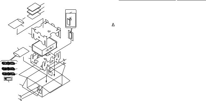
2.1 PACKING
(1) PACKING PARTS LIST
|
|
1 |
Mark |
No. |
Description |
Part No. |
|
|
|
1 |
Instruction Manual |
VRE1074 |
|
|
|
2 (WY Type Only) |
||||
|
|
|
(English/French/German/Italian) |
|
||
|
|
3 (Except |
8 |
|
|
|
|
|
2 |
Instruction Manual |
VRF1045 |
||
|
|
WY/RD |
9 |
|
(Spanish/Portuguese/Dutch/Swedish) |
|
|
|
Type) |
|
|||
|
|
|
NSP |
3 |
Warranty Card |
ARY7022 |
|
|
10 |
|
4 |
Power Cord |
ADG1127 |
|
|
|
5 |
Audio Cord (L=1.5m) |
VDE1033 |
|
|
|
11 |
|
|||
|
|
|
|
|
|
|
|
|
|
|
6 |
Video Cord (L=1.5m) |
VDE1048 |
|
|
|
NSP |
7 |
Battery(R6P,AA) |
VEM-013 |
|
10 |
14 |
|
8 |
Remote Control Unit |
VXX2601 |
|
|
|
|
|
(CU-DV025) |
|
|
|
|
|
9 |
Battery Cover |
VNK4334 |
|
|
12 |
15 |
10 |
Polyethylene Bag |
Z21-038 |
|
4 |
|
16 (Except |
11 |
Protector A |
VHB1065 |
|
|
WY Type) |
||||
|
5 |
|
||||
|
|
|
12 |
Protector B |
VHB1066 |
|
|
6 |
|
|
|||
|
|
|
13 |
Packing Case |
VHG1779 |
|
|
|
|
|
14 |
Mirror Mat Sheet |
VHL1012 |
7 |
13 |
|
|
15 |
Region Label |
See contrast table (2) |
|
|
|
|
|
||
|
|
|
|
16 |
Label |
See contrast table (2) |
|
15 |
|
|
|
|
|
16
(Except WY Type)
(2) CONTRAST TABLE
WY, WY/RD and WY/RE types are constructed the same except for the following :
|
|
|
|
Part No. |
|
|
Mark |
No. |
Symbol and Description |
WY |
WY/RD |
WY/RE |
Remarks |
|
|
|
type |
type |
type |
|
|
2 |
Instruction Manual |
VRF1045 |
Not used |
Not used |
|
|
|
(Spanish/Portuguese/Dutch/Swedish) |
|
|
|
|
NSP |
3 |
Warranty Card |
ARY7022 |
Not used |
ARY7022 |
|
|
15 |
Region Label P2 |
VRW1701 |
Not used |
Not used |
|
|
15 |
Region Label P4 |
Not used |
VRW1705 |
Not used |
|
|
15 |
Region Label P5 |
Not used |
Not used |
VRW1755 |
|
|
16 |
RD Label |
Not used |
VRW1761 |
Not used |
|
|
16 |
RE Label |
Not used |
Not used |
VRW1756 |
|
|
|
|
|
|
|
|
3
DV-717
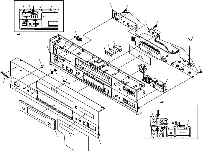
2.2 EXTERIOR SECTION
17
21
22
19
10 11
6 |
7 |
|
|
2 |
6 7 |
|
5 |
|
4 |
1 |
3 |
15
18
14
13
12
9
8 19
20
16
17
Refer to "2.3 FRONT PANEL SECTION"
(1) EXTERIOR SECTION PARTS LIST
Mark No. |
Description |
|
Part No. |
Mark No. |
Description |
|
Part No. |
||
1 |
Door Plate |
|
VAH1312 |
|
11 |
Tray |
|
VNK4333 |
|
2 |
DVD Plate |
|
VAM1077 |
12 |
Clamper |
|
VNL1738 |
||
3 |
Door Panel |
|
VNK4324 |
13 |
Bridge |
|
VNE2069 |
||
4 |
Door Cushion |
|
VEC2008 |
14 |
Clamper Plate |
|
VNE2068 |
||
5 |
Door Holder |
|
VNK4325 |
15 |
Bonnet Case S |
|
VXX2617 |
||
6 |
Door Spring |
|
VBH1305 |
16 |
Screw |
|
BBZ30P080FMC |
||
7 |
Screw |
|
VBA1057 |
17 |
Screw |
|
BCZ40P060FNI |
||
8 |
Spring |
|
VBH1277 |
18 |
Screw |
|
BPZ26P080FZK |
||
9 |
Tray Stopper |
|
VNL1739 |
19 |
Screw |
|
BBT30P080FCC |
||
10 |
Label |
|
VRW1628 |
20 |
Label |
|
VRW1699 |
||
|
|
|
|
|
21 |
PW Joint |
|
VNK4327 |
|
|
|
|
|
|
22 |
Power Button |
|
VNK4159 |
|
4
|
|
|
|
|
|
DV-717 |
2.3 FRONT PANEL SECTION |
|
|
|
|||
7(4/4) |
7(2/4) |
7(3/4) |
7(1/4) |
15 |
17 |
|
|
|
|||||
|
|
|
|
|
14 |
17 |
|
|
|
|
|
|
|
|
|
|
7(2/4) |
|
|
|
:Cut position |
|
|
|
16 |
||
|
11 |
12 |
|
|
10 |
|
|
7(1/4) |
|
|
|
9 |
|
|
|
|
|
|
|
4 |
|
|
|
|
|
8(2/2) |
17 |
|
|
|
|
7(3/4) |
|
|
|
57(4/4) |
|
|
8(1/2) |
3 


 13
13
|
|
:Cut position |
|
|
8(2/2) |
|
|
8(1/2) |
1 |
6 |
|
|
WY/RD |
2 |
|
Type Only |
(1) FRONT PANEL SECTION PARTS LIST
Mark |
No. |
Description |
|
Part No. |
Mark |
No. |
Description |
|
Part No. |
|
1 |
FL Lens |
|
VEC2007 |
|
11 |
Illumi Holder |
|
VNK4098 |
|
2 |
Front Almi |
|
VAH1298 |
|
12 |
FL Filter |
|
VEC2016 |
|
3 |
Name Plate G |
|
PAN1377 |
|
13 |
FLKY Assy |
|
VWG1980 |
|
4 |
LED Lens |
|
PNW2019 |
NSP |
14 |
DIRB Assy |
|
VWG1991 |
|
5 |
LED Lens |
|
VNK4326 |
NSP |
15 |
PWSB Assy |
|
VWG1988 |
NSP |
6 |
Getter |
|
See contrast table (2) |
|
16 |
Flexible Cable |
|
VDA1690 |
|
7 |
Panel Base |
|
VNK4323 |
|
17 |
Screw |
|
BBZ30P080FMC |
|
8 |
Main Key |
|
VNK4095 |
|
|
|
|
|
|
9 |
Illumination Lens |
|
VNK4168 |
|
|
|
|
|
|
10 |
Illumination Filter |
|
VEC1950 |
|
|
|
|
|
(2) CONTRAST TABLE
WY, WY/RD and WY/RE types are constructed the same except for the following :
|
|
|
|
Part No. |
|
|
Mark |
No. |
Symbol and Description |
WY |
WY/RD |
WY/RE |
Remarks |
|
|
|
type |
type |
type |
|
NSP |
6 |
Getter |
Not used |
VRW1757 |
Not used |
|
|
|
|
|
|
|
|
5
DV-717
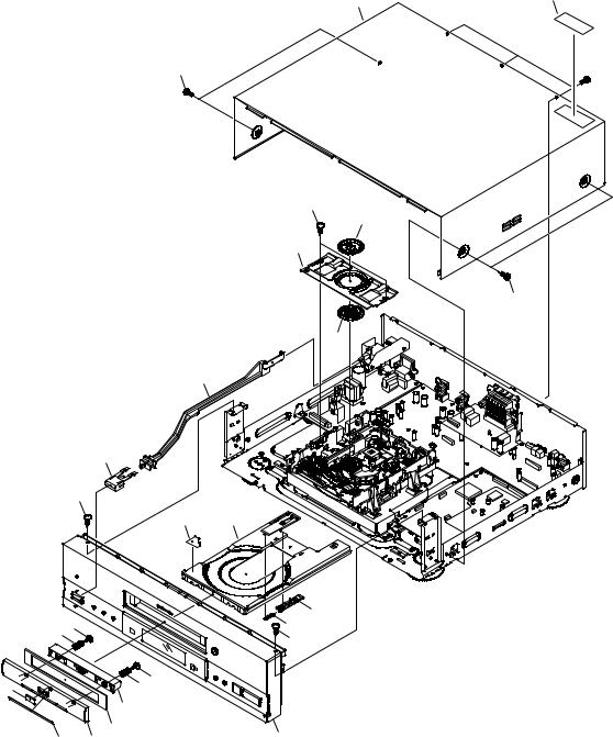
2.4 BOTTOM SECTION
Refer to
"2.5 LOADING MECHANISM ASSY"
|
18 |
|
|
|
19 |
|
|
25 |
32 |
|
|
|
|
||
|
|
26 |
|
10 |
20 |
|
|
20 |
|
||
7 |
11 |
||
|
|||
|
8 |
||
|
|
||
|
33 |
|
|
|
20 |
9 |
|
20 6 |
|
20 |
|
|
|
3
4
5
2
1
20
30
31
17
 29
29
12
28

 7
7
27
6
20
20
21 21
21 34 (Except WY Type)
21
20
13
22
23
24 |
20 |
14
20
15
16
6

DV-717
(1) BOTTOM SECTION PARTS LIST
Mark |
No. |
Description |
|
Part No. |
Mark |
No. |
Description |
|
Part No. |
|
1 |
Insulator |
|
PNW2766 |
|
21 |
Screw |
|
BBZ30P080FMC |
NSP |
2 |
Bottom Plate |
|
PNA2376 |
NSP |
22 |
PC Support Cushion |
|
VEC2033 |
NSP |
3 |
Chassis |
|
VNA1979 |
NSP |
23 |
PC Support Spacer |
|
VEC2032 |
NSP |
4 |
PCB Holder |
|
PNW2029 |
|
24 |
PC Support |
|
DEC1932 |
|
5 |
Flat Cable Clip |
|
VEC2018 |
|
25 |
Flexible Cable (26p) |
|
VDA1688 |
NSP |
6 |
Panel Stay |
|
VNE2156 |
|
26 |
Flexible Cable (12p) |
|
VDA1692 |
NSP |
7 |
PCB Base |
|
RNE1221 |
|
27 |
Flexible Cable (26p) |
|
VDA1694 |
NSP |
8 |
Power-Holder |
|
VNE2123 |
|
28 |
Flexible Cable (22p) |
|
VDA1696 |
NSP |
9 |
P.Plate Holder |
|
PNY-405 |
|
29 |
Connector Assy |
|
PF02PP-S20 |
|
10 |
Power Supply Unit |
|
VWR1306 |
|
30 |
SCRB Assy |
|
VWV1623 |
|
|
|
|
|
|
|
|||
NSP |
11 |
MSWB Assy |
|
VWG1996 |
|
31 |
Flexible Cable (22p) |
|
VDA1699 |
|
12 |
AVJB Assy |
|
VWV1617 |
|
32 |
Housing Assy |
|
VKP2194 |
|
13 |
DNRB Assy |
|
VWV1619 |
|
33 |
Screw |
|
PMB30P080FZK |
|
14 |
DVDM Assy |
|
VWS1349 |
|
34 |
Region Label |
|
See contrast table (2) |
NSP |
15 |
Mecha Holder |
|
VNE2157 |
|
|
|
|
|
|
16 |
Mecha Cushion |
|
VEC2011 |
|
|
|
|
|
|
17 |
Rear Panel |
|
See contrast table (2) |
|
|
|
|
|
NSP |
18 |
Loading Mecha. Assy |
|
VWT1157 |
|
|
|
|
|
|
19 |
Screw |
|
BBZ30P100FMC |
|
|
|
|
|
|
20 |
Screw |
|
ABZ30P080FCC |
|
|
|
|
|
(2) CONTRAST TABLE
WY, WY/RD and WY/RE types are constructed the same except for the following :
|
|
|
|
Part No. |
|
|
Mark |
No. |
Symbol and Description |
WY |
WY/RD |
WY/RE |
Remarks |
|
|
|
type |
type |
type |
|
|
17 |
Rear Panel |
VNA1996 |
VNA2043 |
VNA2043 |
|
|
34 |
Region Label R4 |
Not used |
VRW1704 |
Not used |
|
|
34 |
Region Label R5 |
Not used |
Not used |
VRW1754 |
|
|
|
|
|
|
|
|
7
DV-717
2.5 LOADING MECHANISM ASSY
∙ Top View |
|
|
∙ Bottom View |
|
|
|||
|
|
20 |
|
|
|
|
|
|
|
|
1 |
2 |
|
|
17 |
7 |
|
Refer to |
|
|
|
|
||||
|
|
|
|
|
|
|||
|
|
|
|
|
|
|
||
"2.6 SERVO MECHANISM |
|
|
|
|
|
|
||
ASSY" |
|
|
|
|
|
|
|
|
|
|
|
|
|
18 |
9 |
8 |
|
|
|
19 |
|
|
|
|
||
|
|
|
|
|
|
|
|
|
|
|
|
|
|
|
|
|
16 |
|
3 |
|
|
|
|
|
|
|
|
4 |
|
|
10 |
|
|
|
|
|
|
|
|
|
|
|
|
|
5 |
|
|
|
|
|
|
|
15 |
|
|
|
|
|
|
|
13 |
|
|
|
|
|
|
|
|
|
|
|
|
|
|
|
|
11 |
|
14 |
|
|
|
6 |
|
|
|
12 |
|
|
|
|
|
|
|
|
|
|
LOADING MECHANISM ASSY PARTS LIST |
|
|
|
|
|
|||
Mark |
No. |
Description |
Part No. |
Mark |
No. |
Description |
|
Part No. |
|
1 |
Servo Mechanism Assy-S |
VXX2606 |
|
11 |
Loading Motor Assy |
|
VXX2505 |
|
2 |
Screw |
DBA1006 |
|
12 |
DC Motor / 0.3W |
|
PXM1027 |
|
3 |
Drive Cam |
VNL1736 |
|
13 |
Motor Pulley |
|
PNW1634 |
|
4 |
Drive Gear |
VNL1735 |
NSP |
14 |
LOMB Assy |
|
VWG1886 |
|
5 |
Lock Plate |
VNL1820 |
|
15 |
Connector Assy |
|
VKP2184 |
|
|
|
|
|
|
(LOMB CN401 – LOSB CN306) |
|
|
|
6 |
Loading Base |
VNL1730 |
|
|
|
|
|
|
7 |
Belt |
VEB1260 |
|
16 |
Screw |
|
VBA1055 |
|
8 |
Gear Pulley |
VNL1733 |
|
17 |
Screw |
|
Z39-019 |
NSP |
9 |
LOSB Assy |
VWG1885 |
|
18 |
Flexible Cable (08P) |
|
VDA1698 |
|
10 |
Loading Gear |
VNL1734 |
|
|
(LOSB CN303 – SMEB CN202) |
|
|
|
|
|
|
|
19 |
Float Base |
|
VNL1815 |
|
|
|
|
|
20 |
Floating Rubber |
|
VEB1286 |
8
DV-717
2.6 SERVO MECHANISM ASSY
∙ Top View
|
|
|
|
|
37 |
35 |
33 |
|
38 |
|
18 |
|
|
|
|
||
|
|
28 |
|
10 |
|
30 |
|
15 |
5 |
|
|
|
|
|
|
||
34 |
|
|
|
|
|
16 |
|
|
10 |
|
|
|
|
|
|
||
|
|
|
|
|
|
|
19 |
|
|
13 |
|
|
8 |
|
|
|
|
|
6 |
|
|
37 |
26 |
|
|
|
|
||
|
22 |
|
|
18 |
|
|
|
|
10 |
11 |
|
|
20 |
|
32 |
||
|
33 |
|
14 |
|
25 |
|
|
|
|
|
12 10
27
|
9 |
23 |
|
31 |
7 |
||
|
37
37
21
7
17
2 |
|
29 |
|
24 |
|
|
|
|
|
|
|
7 |
1 |
3 |
36 |
|
|||
|
|
|
|
4 |
|
|
|
SERVO MECHANISM ASSY PARTS LIST
Mark |
No. |
Description |
|
Part No. |
Mark |
No. |
Description |
|
Part No. |
NSP |
1 |
SMEB Assy |
|
VWG1968 |
|
21 |
Hook |
|
VNL1770 |
NSP |
2 |
FGSB Assy |
|
VWG2009 |
|
22 |
FFC Holder |
|
VNL1802 |
|
3 |
Motor |
|
VXM1074 |
|
23 |
Mechanism Base |
|
VNL1806 |
|
4 |
Motor |
|
VXM1075 |
|
24 |
FG Holder |
|
VNL1807 |
|
5 |
Pickup Assy |
|
VWY1050 |
|
25 |
Gear A |
|
VNL1808 |
|
6 |
Table Sheet |
|
DEC2040 |
|
26 |
Gear B |
|
VNL1809 |
|
7 |
Screw |
|
VBA1058 |
|
27 |
Gear C |
|
VNL1810 |
|
8 |
Centering Spring |
|
VBH1278 |
|
28 |
Slider |
|
VNL1811 |
|
9 |
Hook Spring |
|
VBH1291 |
|
29 |
Gear D |
|
VNL1814 |
|
10 |
Skew Spring |
|
VBH1303 |
NSP |
30 |
Magnet |
|
VYM1024 |
|
11 |
Gear Spring |
|
VBH1308 |
|
31 |
Screw |
|
JFZ17P025FZK |
NSP |
12 |
Reflected Sheet |
|
VEC1959 |
|
32 |
Screw |
|
JGZ17P028FMC |
|
13 |
Guide Bar |
|
VLL1504 |
|
33 |
Screw |
|
VBA1051 |
|
14 |
Sub-guide Bar |
|
VLL1505 |
|
34 |
Magnet Holder Assy |
|
VXX2507 |
|
15 |
Hold Spring |
|
VNC1017 |
|
35 |
Spindle Motor Assy |
|
VXX2604 |
NSP |
16 |
Magnet Holder |
|
VNE2070 |
|
36 |
Carriage Motor Assy |
|
VXX2605 |
NSP |
17 |
Motor Base |
|
VNE2154 |
|
37 |
Screw |
|
PBA1069 |
NSP |
18 |
Cover |
|
VNE2155 |
|
38 |
Flexible Cable (24P) |
|
VDA1701 |
|
19 |
Centering Ring |
|
VNL1746 |
|
|
(DVDM CN120 – Pickup Assy) |
|
|
NSP |
20 |
Disc Table |
|
VNL1747 |
|
|
|
|
|
9
|
1 |
|
2 |
|
3 |
|
4 |
|
|
|
|
|
|
DV-717
3. SCHEMATIC DIAGRAM
3.1 OVERALL CONNECTION DIAGRAM, LOMB,
LOSB, SMEB and FGSB ASSEMBLIES
A
K SCRB ASSY
(VWV1623) CN1001
 CN103
CN103
I I 1/2, I 2/2
AVJB ASSY (VWV1617)
B
CN102
C
J J 1/2, J 2/2
DNRB ASSY (VWV1619)
H H 1/3 H 3/3
DVDM ASSY (VWS1349)
CN602
G DILB ASSY
(VWG1991)
E
D
F |
PWSB ASSY |
FLKY ASSY |
|
(VWG1980) |
|||
|
(VWG1988) |
||
|
|
FLKB ASSY (VWM1860)
10
|
1 |
|
2 |
|
3 |
|
4 |
|
|
|
|
|
|
||||
|
|
|
|
|
|
5 |
|
6 |
|
7 |
|
8 |
|
|
|
|
|
|
DV-717
Note : When ordering service parts, be sure to refer to "EXPLODED VIEWS and PARTS LIST" or "PCB PARTS LIST".
A
L
MSWB ASSY (VWG1996)
M
POWER
SUPPLY ASSY (VWR1306)
B
|
: RF SIGNAL ROUTE |
|
PICKUP ASSY |
(F) : FOCUS SERVO LOOP LINE |
|
(VWY1050) |
(T) |
|
: TRACKING SERVO LOOP LINE |
||
(F) |
(S) |
|
: SLIDER SERVO LOOP LINE |
||
(F) |
||
|
||
(T) |
|
D FGSB ASSY (VWG2009)
(F)
|
(T) |
R101 |
|
680 |
|
|
(T) |
|
|
|
|
|
(F) |
C |
|
|
|
CN301 |
CN302 |
|
|
|
|
|
(S) |
(S) |
(S) |
(S) |
(S) |
|
|
|
(S) |
|
CARRIAGE MOTOR ASSY |
|
|
|
|
|
VXX2605 |
|
|
C |
B |
LOSB ASSY |
SMEB ASSY |
(VWG1885) |
(VWG1968) |
|
|
CN303 |
|
|
B2B-PH-K-S |
|
A LOMB ASSY (VWG1886)
CN401
B2B-PH-K-S
D
SPINDLE MOTOR ASSY
VXX2604
LOADING MOTOR ASSY :VXX2505
A 
 B
B 
 C
C 
 D 11
D 11
|
5 |
|
6 |
|
7 |
|
8 |
|
|
|
|
|
|
||||
|
|
|
|
|
|
1 |
|
2 |
|
3 |
|
4 |
|
|
|
|
|
|
DV-717
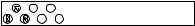
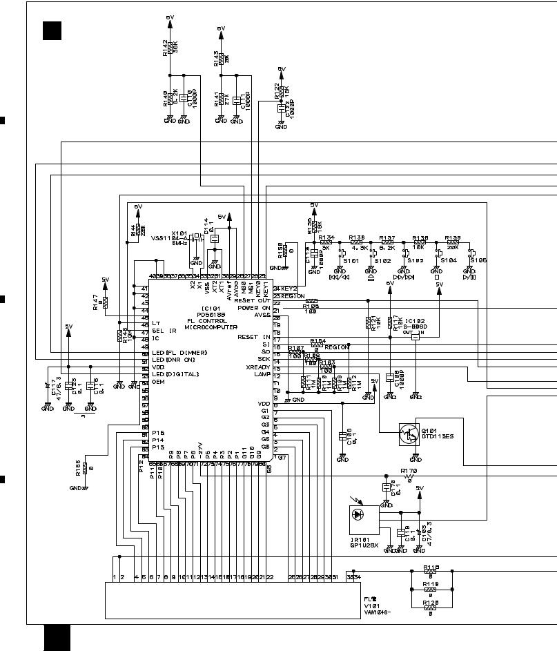
3.2 FLKY, PWSB and DILB ASSEMBLIES
A
E FLKY ASSY (VWG1980)
B
C
D
12 E
|
1 |
|
2 |
|
3 |
|
4 |
|
|
|
|
|
|
||||
|
|
|
|
|
|
5 |
|
6 |
|
7 |
|
8 |
|
|
|
|
|
|
DV-717
F PWSB ASSY (VWG1988)
A
B
H 2/3
CN602
FLKB ASSY (VWM1860)
C
G
DILB ASSY (VWG1991)
SWITCHES:
FLKY ASSY D S101: 4/1
S102: 0 S103: Á/¢ S104: 7 S105: 6
E 
 F
F 
 G 13
G 13
|
5 |
|
6 |
|
7 |
|
8 |
|
|
|
|
|
|
||||
|
|
|
|
|

A
B
C
D
1 |
|
2 |
|
3 |
|
4 |
|
|
|
|
|
DV-717
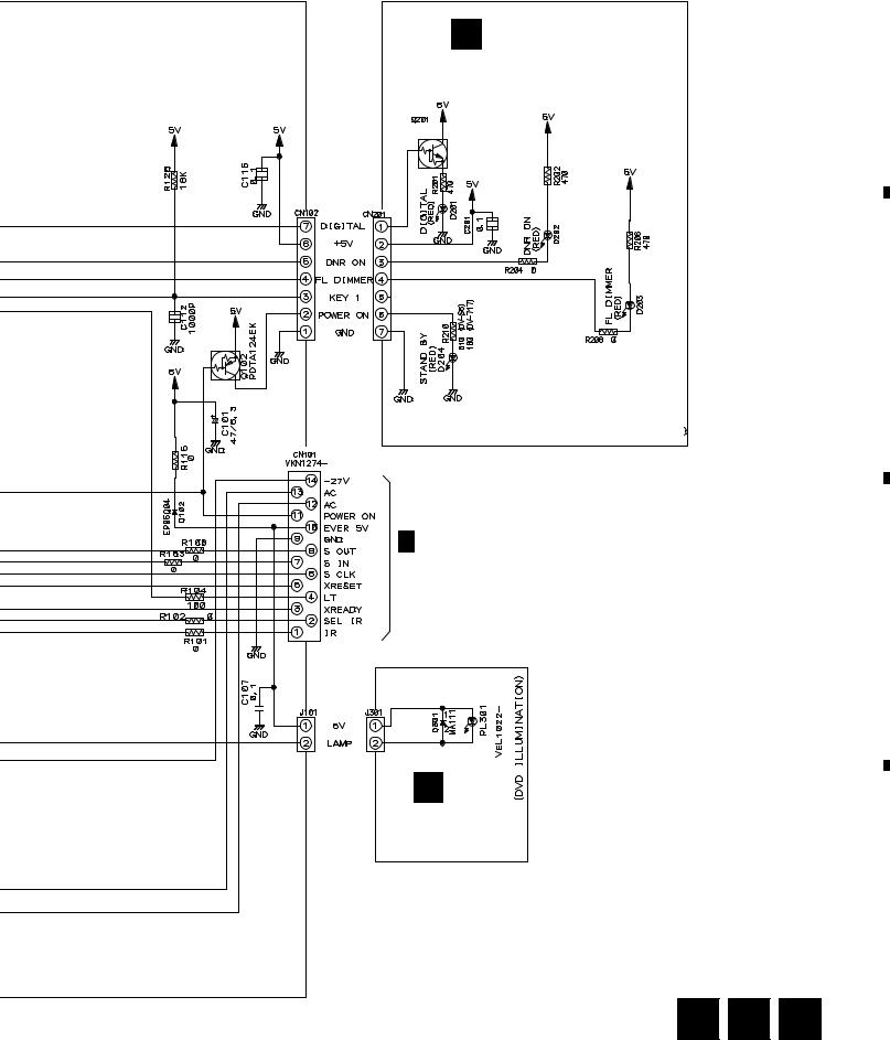
3.3 DVDM ASSY (1/3)
|
|
(5/6) |
2/3 |
(2/6) |
|
|
|
|
|
|
(6/6) |
|
(3/6) |
(1/6) |
|
|
1/2 |
1 |
|
from IC261 |
|
|
(4/6) |
|
|
to IC501 |
|
|
|
|
|
2/2 |
|
|
|
|
|
|
|
|
|
|
|
|
|
|
|
(DVD) |
|
|
|
|
|
|
|
|
|
|
ADC1175CIJMX |
|
|
|
|
|
|
|
|
(DVD) |
|
|
|
|
|
|
|
|
3 |
|
|
to IC501 |
|
|
|
|
|
(DVD) |
|
|
|
|
|
|
|
|
|
|
|
H 2/3 |
|
|
|
|
|
(DVD) |
|
|
|
|
|
|
|
|
|
|
|
|
|
|
(DVD) |
|
|
to IC701 |
|
|
|
|
|
|
|
H 2/3 |
|
|
|
|
|
|
|
|
|
|
CN103 |
|
|
|
|
|
|
|
(CD) |
|
|
|
|
|
|
|
2 |
|
|
|
|
|
|
|
|
|
to CN120 |
|
|
(F) |
|
|
|
(CD) |
|
|
M |
|
|
|
|
|
|
(F) |
(F) |
|
|
|
|
|
|
|
||
|
|
(T) |
|
|
|
|
(T) |
4 |
|
|
|
|
|
|
|
||
|
|
|
|
|
|
|
|
|
|
|
|
|
|
|
|
|
(T) |
|
|
(T) |
|
|
|
|
|
|
|
|
(F) |
|
|
|
|
|
|
|
|
(F) |
|
|
|
|
|
|
|
|
to |
|
|
|
|
|
|
|
|
IC501 |
|
|
|
|
|
|
|
|
(F) |
|
|
|
|
|
|
ASSY |
|
(F) |
|
|
|
|
|
|
|
(T) |
|
|
|
|
|
|
|
|
|
|
|
|
|
|
|
|
PICKUP |
|
(S) |
|
|
|
|
|
to IC501 |
|
|
|
|
|
|
|
|
|
|
|
(F) |
|
|
(S) |
|
|
|
|
|
(T) |
|
|
|
|
|
|
|
|
(T) |
|
|
|
|
|
2/2 |
|
|
(F) |
|
|
|
|
|
|
|
|
|
|
|
|
|
|
1/2 |
|
CN301 |
|
|
|
|
|
|
|
|
B |
(S) |
|
|
|
|
|
|
|
(S) |
(T) |
(T) |
(F) |
(F) |
|
|
|
|
|
|
|
|
|
|
|
|
|
|
(F) |
(T) |
|
|
|
|
|
14 |
H 1/3 |
|
|
|
|
|
|
|
|
1 |
2 |
|
|
|
3 |
|
4 |
5 |
6 |
7 |
|
8 |
|
|
|
|
|
DV-717 |
|
from Q107,Q108 |
H 1/3 DVDM ASSY(1/3) (VWS1349) |
|
|||
|
|
||||
|
to IC101 |
|
|
|
|
IC507 |
CN120 |
|
|
|
A |
TC74VHCT245AFT |
|
|
|
||
|
to |
|
|
|
|
to IC101 |
|
|
|
|
|
|
1/2 |
2/2 |
|
|
|
|
(1/2) |
|
|
|
|
|
3/3 |
|
|
|
|
|
|
|
|
|
B |
|
|
(2/2) |
|
|
|
|
|
|
2/3 |
|
|
|
|
6 |
to IC601 |
|
|
|
(CD) |
|
|
|
|
|
|
|
|
|
|
|
|
|
2/3 |
|
|
|
|
|
to IC701 |
|
|
(T) |
(T) |
|
|
|
|
|
|
|
|
|
|
(F) |
(F) |
|
|
|
|
|
|
|
|
|
|
|
(CD) |
|
|
|
|
|
5 |
|
|
|
|
(CD) |
|
|
|
|
|
(S) |
(S) |
|
|
|
C |
(F) |
(F) |
|
|
|
|
|
|
|
|
||
(T) |
|
|
|
|
|
(T) |
|
|
|
|
|
|
|
|
|
|
|
(CD) |
|
|
|
|
|
(CD) |
|
|
|
|
|
|
|
|
8 |
|
|
|
|
|
9 |
|
|
7 |
|
|
|
|
|
|
|
2/2 |
|
|
|
|
|
10 |
11 |
|
|
|
|
to IC302 |
|
|
|
|
|
1/2 |
2/3 |
|
|
|
|
|
|
|
|
LEVEL SHIFT |
: RF SIGNAL ROUTE |
|
|
|
D |
|
: ROM DATA SIGNAL ROUTE |
|
|
|
|
|
(F) |
|
|
|
|
|
: FOCUS SERVO LOOP LINE |
|
|
|
|
|
(T) |
|
|
|
|
|
: TRACKING SERVO LOOP LINE |
|
|
|
|
|
(S) |
|
|
|
|
|
: SLIDER SERVO LOOP LINE |
|
|
|
|
|
|
|
H |
1/3 |
15 |
|
|
|
|
||
|
5 |
|
6 |
|
7 |
|
8 |
|
|
|
|
|
|
||||
|
|
|
|
|
|
1 |
|
2 |
|
3 |
|
4 |
|
|
|
|
|
|
DV-717
3.4 DVDM ASSY (2/3)
A |
|
|
H 2/3 |
DVDM ASSY(2/3) |
|
|
|
||
|
|
|
|
(VWS1349) |
|
|
|
3/3 |
|
|
|
|
XCSDOLV,XCS6,XWRL,XWRH,XLT3, |
|
|
|
|
XAMUTE,XDACK1,XDREQ1,IR,SEL-IR, |
|
|
|
|
48/44,XDVRST1,XAVIRQ0,NSP-SW, |
|
|
|
|
SSCK,SSO,XRESET |
|
|
|
VYW1518 |
|
|
B |
|
|
|
|
|
|
|
|
3/3 |
|
|
|
|
ADDRESS |
|
|
|
|
A2–A10 |
|
|
|
|
3/3 |
|
|
|
|
DATA |
C |
|
|
|
|
|
|
|
1/3 |
|
|
IC605(1/2) |
|
|
|
|
TC74VHC139FT |
|
|
|
|
|
|
|
1/3 |
|
IC605(2/2) |
|
|
|
|
TC74VHC139FT |
|
|
|
D |
|
|
|
|
16 |
H 2/3 |
|
|
|
|
1 |
2 |
3 |
4 |
5 |
6 |
|
7 |
8 |
|
|
|
|
|
|
DV-717 |
|
|
: AUDIO SIGNAL ROUTE |
|
|
|
|
|
|
: ROM DATA SIGNAL ROUTE |
|
3/3 |
|
|
A |
|
|
|
|
from IC801 |
|
|
|
|
|
|
from IC701 |
|
|
|
|
|
|
|
|
3/3 |
|
|
|
|
IC703 |
1/3 |
|
|
|
|
|
|
|
|
|
|
|
|
TC74VHCT541AFT |
|
|
|
(DVD) |
3/3 |
|
3/3 |
|
|
|
|
SDATA |
|
|
|
|
|
(DVD) |
|
|
|
1/3 |
|
B |
|
|
(DVD) |
from IC301 |
|
||
|
|
|
|
|
||
|
|
|
|
|
|
|
(DVD) |
|
|
|
|
|
|
|
MONITOR OUTPUT |
|
|
|
|
|
|
|
|
|
1/3 |
|
|
|
|
|
from IC301 |
1/3 |
|
|
|
|
|
|
|
|
C |
|
SERVO |
|
|
3/3 |
|
|
|
|
|
|
|
||
1/3 |
|
|
|
|
|
|
|
|
|
|
1/3 |
|
|
|
|
|
|
1/3 |
|
|
|
|
|
to IC801 |
3/3 |
|
|
|
3/3 |
|
(CD) |
|
|
|
|
E |
|
|
|
|
|
|
CN101 |
|
|
|
|
|
|
to IC801 |
from IC201 |
|
|
|
|
|
3/3 |
1/3 |
|
|
|
|
|
1/3 |
|
|
D |
||
|
|
|
|
|
|
|
|
|
|
|
H 2/3 |
17 |
|
|
|
|
|
|
|
|
|
5 |
|
6 |
|
7 |
|
8 |
|
|
|
|
|
|
||||
|
|
|
|
|
|
1 |
|
2 |
|
3 |
|
4 |
|
|
|
|
|
|
DV-717
3.5 DVDM ASSY (3/3) |
|
|
IC810(1/4) |
||
TC74VHC00FT |
||
|
IC810(2/4) |
|
A |
TC74VHC00FT |
|
2/3 |
||
2/3 |
||
IC810(3/4) |
||
|
||
IC810(4/4) |
TC74VHC00FT |
|
TC74VHC00FT |
||
2/3 |
|
|
|
2/3 |
|
B |
|
|
|
2/3 |
|
|
(DVD) |
|
IC801 |
|
|
MB86371C |
|
|
|
(DVD) |
|
|
from IC701 |
|
C |
2/3 |
|
|
||
from IC701
 2/3
2/3
from IC701
 2/3
2/3
D
18 H 3/3
|
1 |
|
2 |
|
3 |
|
4 |
|
|
|
|
|
|
||||
|
|
|
|
|
|
5 |
|
6 |
|
7 |
|
8 |
|
|
|
|
|
|
DV-717
CLOCK GENERATOR SECTION
IC906(1/3) |
for IC801 |
IC906 : IC906(3/3)
TC7W04F
A
IC906(2/3) 
 2/3 H 3/3 DVDM ASSY(3/3)
  (VWS1349)
for IC801
IC904(1/3) |
|
|
|
IC904(2/3) |
2/3 |
2/3 |
|
1 |
|
||
IC904 : |
for IC701 |
2 |
|
3 |
|
||
TC7W04F |
|
|
|
|
1/3 |
4 |
|
|
5 |
|
|
|
for IC201 |
6 |
|
IC904(3/3) |
7 |
|
|
|
B |
||
|
|
8 |
|
|
|
9 |
|
|
|
10 |
|
|
|
11 |
I 1/2 |
|
|
12 |
|
|
|
13 |
|
|
|
14 |
CN101 |
|
|
15 |
|
|
|
16 |
|
|
|
17 |
|
|
|
18 |
|
|
|
19 |
|
|
|
20 |
|
|
|
21 |
|
: AUDIO SIGNAL ROUTE |
|
22 |
|
|
23 |
|
|
|
|
|
|
: ROM DATA SIGNAL ROUTE |
24 |
|
|
(V/CB) |
|
25 |
|
: V/CB SIGNAL ROUTE |
|
26 |
|
(Y) |
|
|
|
: Y SIGNAL ROUTE |
|
|
|
(C) |
|
|
|
: C SIGNAL ROUTE |
|
|
|
 2/3
2/3
|
17 |
1 |
|
|
|
|
|
|
18 |
2 |
R |
|
3 |
|
|
|
|
|
|
|
15 |
4 |
|
|
5 |
|
|
|
|
6 |
B |
|
|
7 |
|
|
|
8 |
|
|
|
9 |
|
|
|
10 |
|
|
|
11 |
|
|
|
12 |
|
|
|
13 |
|
|
|
14 |
|
|
|
15 |
|
|
14 |
16 |
|
|
17 |
|
|
(C) |
|
18 |
|
13 16 |
19 |
|
|
(Y) |
|
20 |
|
|
21 |
|
|
|
|
|
|
|
|
22 |
|
C
I 2/2
CN102
D
H 3/3 19
|
5 |
|
6 |
|
7 |
|
8 |
|
|
|
|
|
|
||||
|
|
|
|
|
DV-717
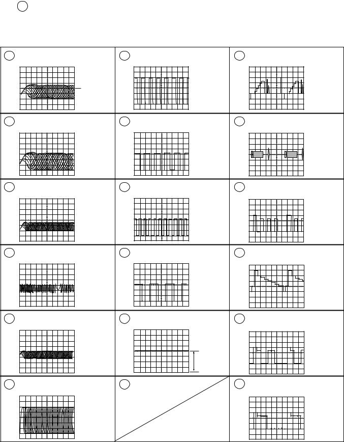
• WAVEFORMS OF DVDM ASSY
Note : No. in the table correspond to the number on the schematic diagram. |
|
|
|||
Measurement condition : No. 1 to 4 and 6 to 11 |
: Disc MJK1, Title 1-chp 1 |
|
|
||
|
No. 5 |
: CD, ABEX-784 Track 1 |
|
|
|
|
No. 13 to 14 |
: MJK1, Title 1-chp 4 |
|
|
|
|
No. 15 to 18 |
: MJK1, Title 1-chp 5 |
|
|
|
1 |
Q109-Emitter (RF) |
7 |
Q281-Collector (FG) |
13 |
CN9031-pin 20 (Y output) |
|
V: 100mV/div. H: 0.1μS/div. |
|
V: 1V/div. H: 5mS/div. |
|
V: 500mV/div. H: 10μS/div. |
|
DC 2V |
|
|
|
|
2 |
TP (RFO) |
8 |
Foot of R261 (FPWM) |
14 |
CN9031-pin 18 (C output) |
|
V: 500mV/div. H: 0.1μS/div. |
|
V: 1V/div. H: 10μS/div. |
|
V: 500mV/div. H: 10μS/div. |
3 IC301-pin 19 (RF for A/D converter) |
9 Foot of R262 (VPWM) |
15 |
CN9031-pin 6 (B output when |
|
selecting color difference output) |
||||
V: 1V/div. H: 0.2μS/div. |
V: 1V/div. H: 10μS/div. |
|
||
|
V: 500mV/div. H: 10μS/div. |
|||
|
|
|
4 TP (Tracking Error) |
10 Foot of R263 (PPWM) |
16 |
CN9031-pin 20 (Y output when |
|
selecting color difference output) |
||||
V: 1V/div. H: 2mS/div. |
V: 1V/div. H: 0.2μS/div. |
|
||
|
V: 500mV/div. H: 10μS/div. |
|||
|
|
|
5 IC201-pin 39 (EFM before slice) |
11 Foot of R264 (RPWM) |
17 |
CN9031-pin 2 (R output when |
|
selecting color difference output) |
||||
V: 1V/div. H: 1μS/div. |
|
|
||
|
|
V: 500mV/div. H: 10μS/div. |
||
|
|
|
|
|
DC1.4V |
|
|
6 IC201-pin 1 (EFM) |
12 |
18 |
CN9031-pin 4 (G output when |
|
selecting color difference output) |
||||
V: 1V/div. H: 0.2μS/div. |
|
|
||
|
|
V: 500mV/div. H: 10μS/div. |
||
|
|
|
20
 Loading...