

Page 1
PIONEER CORPORATION 4-1, Meguro 1-chome, Meguro-ku, Tokyo 153-8654, Japan
PIONEER ELECTRONICS (USA) INC. P.O. Box 1760, Long Beach, CA 90801-1760, U.S.A.
PIONEER EUROPE NV Haven 1087, Keetberglaan 1, 9120 Melsele, Belgium
PIONEER ELECTRONICS ASIACENTRE PTE. LTD. 253 Alexandra Road, #04-01, Singapore 159936
PIONEER CORPORATION 2005
DVD PLAYER DV-686A-S
STANDBY/ON
DV-686A-S
OPEN/CLOSE
TOP MENU MENU
HOME
MENU
RETURN
ORDER NO.
RRV3181
DVD PLAYER
DV-686A-S
THIS MANUAL IS APPLICABLE TO THE FOLLOWING MODEL(S) AND TYPE(S).
Model Type Power Requirement Region No.
DV-686A-S RLFXTL AC110-127V/220-240V 3 Automatic select
DV-686A-S WPWXTL AC220-240V 4 —
The voltage can be converted
by the following method.
For details, refer to "Important Check Points for Good Servicing" .
T-ZZR MAY 2005 printed in Japan
Page 2
1234
SAFETY INFORMATION
A
This service manual is intended for qualified service technicians ; it is not meant for the casual doit-yourselfer. Qualified technicians have the necessary test equipment and tools, and have been
trainedto properly and safely repair complex products such as those covered by this manual.
Improperly performed repairs can adversely affect the safety and reliability of the product and
may void the warranty. If you are not qualified to perform the repair of this product properly and
safely, you should not risk trying to do so and refer the repair to a qualified service technician.
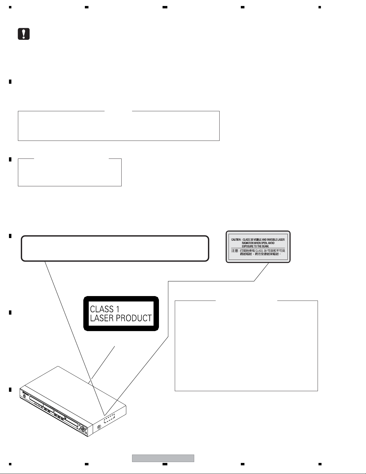
WARNING !
THE AEL (ACCESSIBLE EMISSION LEVEL) OF THE LASER POWER OUTPUT IS LESS THAN CLASS 1
B
BUT THE LASER COMPONENT IS CAPABLE OF EMITTING RADIATION EXCEEDING THE LIMIT FOR
CLASS 1.
A SPECIALLY INSTRUCTED PERSON SHOULD DO SERVICING OPERATION OF THE APPARATUS.
LASER DIODE CHARACTERISTICS
FOR DVD : MAXIMUM OUTPUT POWER : 5 mW
FOR CD : MAXIMUM OUTPUT POWER : 5 mW
WAVELENGTH : 650 nm
WAVELENGTH : 780 nm
C
LABEL CHECK
Location: inside of the unit
: VISIBLE AND INVISIBLE LASER RADIATION WHEN OPEN. AVOID EXPOSURE TO BEAM.
: SICHTBARE UND UNSICHTBARE LASERSTRAHLUNG,WENNABDECKUNG GEÖFFNET NICHT DEM STRAHL AUSSETZEN !
: SYNLIG OG USYNLIG LASERSTRÅLING VED ÅBNING UNDGÅ UDSÆTTELSE FOR STRÀLING.
: SYNLIG OCH OSYNLIG LASERSTRÅLNING NÄR DENNA DEL ÄR ÖPPNAD BETRAKTA EJ STRÅLEN.
: AVATTAESSA ALTISTUT NÄKYVÄ JA NÄKYMÄTTÖMÄLLE LASERSATEIL YLLE. ÄLÄ KATSO SÄTEESEN.
: RADIACIÓN LÁSER VISIBLE E INVISIBLE AL ESTAR ABIERTO. EVITAR EXPOSICIÓN AL RAYO.
D
E
CAUTION
VORSICHT
ADVARSEL
VARNING
VARO!
CUIDADO
(Printed on the Rear Panel)
7260000356 SH
726000A114 SH
for /WPWXTL model
Additional Laser Caution
1.
• Laser diode is driving with Q2303,Q2305(650nm LD) and Q2302,
Q2304(780nm LD)on the DVD MT PCB Assy.
Therefore, when short-circuit between the emitter and collector of these
transistors or the base voltage is supplied for transistors turn on, the
laser oscillates. (failure mode)
• In the test mode ∗ , there is the mode that the laser oscillates except
for the disc judgment and playback. LD ON mode in the test mode
oscillates with the laser forcibly.
2. When the cover is open, close viewing through the objective lens with
the naked eye will cause exposure to the laser beam.
726000A114
for /RLFXTL model
∗ : See page 51.
F
2
DV-686A-S
1234
Page 3
5678
[Important Check Points for Good Servicing]
In this manual, procedures that must be performed during repairs are marked with the below symbol.
Please be sure to confirm and follow these procedures.
1. Product safety
Please conform to product regulations (such as safety and radiation regulations), and maintain a safe servicing environment by
following the safety instructions described in this manual.
1 Use specified parts for repair.
Use genuine parts. Be sure to use important parts for safety.
2 Do not perform modifications without proper instructions.
Please follow the specified safety methods when modification(addition/change of parts) is required due to interferences such as
radio/TV interference and foreign noise.
3 Make sure the soldering of repaired locations is properly performed.
When you solder while repairing, please be sure that there are no cold solder and other debris.
Soldering should be finished with the proper quantity. (Refer to the example)
4 Make sure the screws are tightly fastened.
Please be sure that all screws are fastened, and that there are no loose screws.
5 Make sure each connectors are correctly inserted.
Please be sure that all connectors are inserted, and that there are no imperfect insertion.
6 Make sure the wiring cables are set to their original state.
Please replace the wiring and cables to the original state after repairs.
In addition, be sure that there are no pinched wires, etc.
7 Make sure screws and soldering scraps do not remain inside the product.
Please check that neither solder debris nor screws remain inside the product.
8 There should be no semi-broken wires, scratches, melting, etc. on the coating of the power cord.
Damaged power cords may lead to fire accidents, so please be sure that there are no damages.
If you find a damaged power cord, please exchange it with a suitable one.
9 There should be no spark traces or similar marks on the power plug.
When spark traces or similar marks are found on the power supply plug, please check the connection and advise on secure
connections and suitable usage. Please exchange the power cord if necessary.
0 Safe environment should be secured during servicing.
When you perform repairs, please pay attention to static electricity, furniture, household articles, etc. in order to prevent injuries.
Please pay attention to your surroundings and repair safely.
A
B
C
D
2. Adjustments
To keep the original performance of the products, optimum adjustments and confirmation of characteristics within specification.
Adjustments should be performed in accordance with the procedures/instructions described in this manual.
3. Lubricants, Glues, and Replacement parts
Use grease and adhesives that are equal to the specified substance.
Make sure the proper amount is applied.
4. Cleaning
For parts that require cleaning, such as optical pickups, tape deck heads, lenses and mirrors used in projection monitors, proper
cleaning should be performed to restore their performances.
5. Shipping mode and Shipping screws
To protect products from damages or failures during transit, the shipping mode should be set or the shipping screws should be
installed before shipment. Please be sure to follow this method especially if it is specified in this manual.
56
DV-686A-S
E
F
3
7
8
Page 4

1234
CONTENTS
SAFETY INFORMATION ..................................................................................................................................... 2
1. SPECIFICATIONS ............................................................................................................................................ 5
2. EXPLODED VIEWS AND PARTS LIST ............................................................................................................ 6
A
B
C
D
2.1 PACKING SECTION .................................................................................................................................. 6
2.2 EXTERIOR SECTION............................................................................................................................... 8
2.3 05 DVD MECHA SECTION...................................................................................................................... 10
3. BLOCK DIAGRAM AND SCHEMATIC DIAGRAM..........................................................................................12
3.1 BLOCK DIAGRAM ................................................................................................................................... 12
3.2 OVERALL WIRING CONNECTION DIAGRAM........................................................................................ 14
3.3 DVD MT PCB (1/6) ASSY........................................................................................................................ 16
3.4 DVD MT PCB (2/6) ASSY........................................................................................................................ 18
3.5 DVD MT PCB (3/6) ASSY........................................................................................................................ 20
3.6 DVD MT PCB (4/6) ASSY........................................................................................................................ 22
3.7 DVD MT PCB (5/6) ASSY........................................................................................................................ 24
3.9 OPERATION, OPERATION 2 and OPERATION 3 PCB ASSYS ............................................................. 28
3.10 POWER PCB (1/2) ASSY ...................................................................................................................... 30
3.11 POWER PCB (2/2) ASSY ...................................................................................................................... 32
3.12 WAVEFORMS ........................................................................................................................................ 34
4. PCB CONNECTION DIAGRAM ..................................................................................................................... 37
4.1 LOADING and SW PCB ASSYS.............................................................................................................. 37
4.2 DVD MT PCB ASSY................................................................................................................................. 38
4.3 OPERATION, OPERATION 2 and OPERATION 3 PCB ASSYS ............................................................. 42
4.4 POWER PCB ASSY................................................................................................................................. 46
5. PCB PARTS LIST ........................................................................................................................................... 48
6. ADJUSTMENT ............................................................................................................................................... 50
6.1 WHEN REPLACING DVD DECK ............................................................................................................. 50
6.2 TEST MODE ............................................................................................................................................ 51
6.3 TEST MODE IN........................................................................................................................................ 52
6.4 DISC REMOVAL METHOD...................................................................................................................... 53
7. GENERAL INFORMATION............................................................................................................................. 54
7.1 DIAGNOSIS ............................................................................................................................................. 54
7.1.1 DISPLAY SPECIFICATION OF THE TEST MODE............................................................................ 54
7.1.2 FUNCTIONAL SPECIFICATION OF THE SHORTCUT KEY ............................................................ 55
7.1.3 SPECIFICATION OF MODEL INFORMATION DISPLAY .................................................................. 56
7.1.4 FUNCTIONAL SPECIFICATION OF THE SERVICE MODE............................................................. 57
7.1.5 METHOD FOR DIAGNOSING DEGRADATION OF THE LDS ON THE PICKUP ASSY .................. 58
7.1.6 TROUBLE SHOOTING...................................................................................................................... 59
7.2 DISASSEMBLY ........................................................................................................................................ 61
7.3 DVD DECK SECTION.............................................................................................................................. 62
7.4 IC INFORMATION.................................................................................................................................... 66
8. PANEL FACILITIES ........................................................................................................................................ 78
8.1 FRONT PANEL SECTION ....................................................................................................................... 78
8.2 DISPLAY .................................................................................................................................................. 79
8.3 REMOTE CONTROL ............................................................................................................................... 80
E
F
4
1234
DV-686A-S
Page 5

5678
1. SPECIFICATIONS
Specifications
A
General
System . . . . . . . . . . . . . . . . . . . . . . DVD player
Power requirements
Australia model. . . . . . . . AC
Other models
. . AC 110–127/220–240 V, 50/60 Hz
220–240 V, 50/60 Hz
Power consumption . . . . . . . . . . . . . . . . . 8 W
Power consumption (standby) . . . . . . 0.85 W
Weight . . . . . . . . . . . . . . . . . . . . . . . . 1.7kg
Dimensions:
. . . 420 (W) x 49.5 (H) x 225.5 (D) mm
Operating temperature . . . . . . . +5°C to +35°C
(+41°F to +95°F)
Operating humidity . . . . . . . . . . . . . 5% to 85%
(no condensation)
Component video output
Y (luminance) - Output level . . . 1 Vp-p (75 Ω )
(color) - Output level
P
B
P
(color) - Output level . . . . . 0.7 Vp-p (75 Ω)
R
. . . . . . . . . . . . . . . . . . . . . . . . . . . . . . RCA
Jack
. . . . 0.7 Vp-p (75Ω )
Audio output (multi-channel / L, R, C, SW,
SL, SR)
Output level . . . . . . . . . . . . . During audio output
Number of channels . . . . . . . . . . . . . . . . . . . . . 6
Jacks . . . . . . . . . . . . . . . . . . . . . . . . . . . . RCA jack
200 mVrms (1 kHz, –20 dB)
Digital audio characteristics
Frequency response . . . . . . . . 4 Hz to 44 kHz
(DVD fs: 96 kHz)
4 Hz to 88 kHz (DVD-Audio fs: 192 kHz)
S/N ratio . . . . . . . . . . . . . . . . . . . . . . . . . 115 dB
Dynamic range . . . . . . . . . . . . . . . . . . . . 101 dB
Total harmonic distortion . . . . . . . . . . 0.0023 %
Wow and flutter . . . . . . Limit of measurement
(±0.001% W. PEAK) or lower
Digital output
Coaxial digital output . . . . . . . . . . . . .
Optical digital output . . . . . . . Optical digital jack
RCA jack
B
C
S-video output
Y (luminance) - Output level . . . . . 1 Vp-p (75 Ω)
C (color) - Output level . . . . . . 286 mVp-p (75 Ω)
Jack . . . . . . . . . . . . . . . . . . . . . . . . . . . . S-video
Video output
Output level. . . . . . . . . . . . . . . . . . 1 Vp-p (75 Ω)
Jack. . . . . . . . . . . . . . . . . . . . . . . . . . . . . . . RCA
Audio output (1 stereo pair)
Output level . . . . . . . . . . . . During audio output
Number of channels . . . . . . . . . . . . . . . . . . . . . 2
Jacks . . . . . . . . . . . . . . . . . . . . . . . . . . . . . . .
200 mVrms (1 kHz, –20 dB)
RCA
Accessories
Audio/video cable. . . . . . . . . . . . . . . . . . . . . . . . 1
Power cable
Singapore and Taiwan model
Others . . . . . . . . . . . . . . . . . . . . . . . . . . . . . . . . . 1
Remote control . . . . . . . . . . . . . . . . . . . . . . . . . . 1
AA/R6P dry cell batteries
Front panel button names sticker
(Singapore/Taiwan models only) .
Remote control overlay
(Singapore/Taiwan models only) . . .
Operating Instructions
The specifications and design of this product are subject to
change without notice, due to improvement.
Published by Pioneer Corporation.
Copyright © 2005 Pioneer Corporation.
. . . . . . . . . . . . . . 2
. . . . . . . . . . . . . . . . . . . 2
. . . . . . . . . . . 1
. . . . . . . . . . . 1
All rights reserved
D
E
56
DV-686A-S
F
5
7
8
Page 6
1234
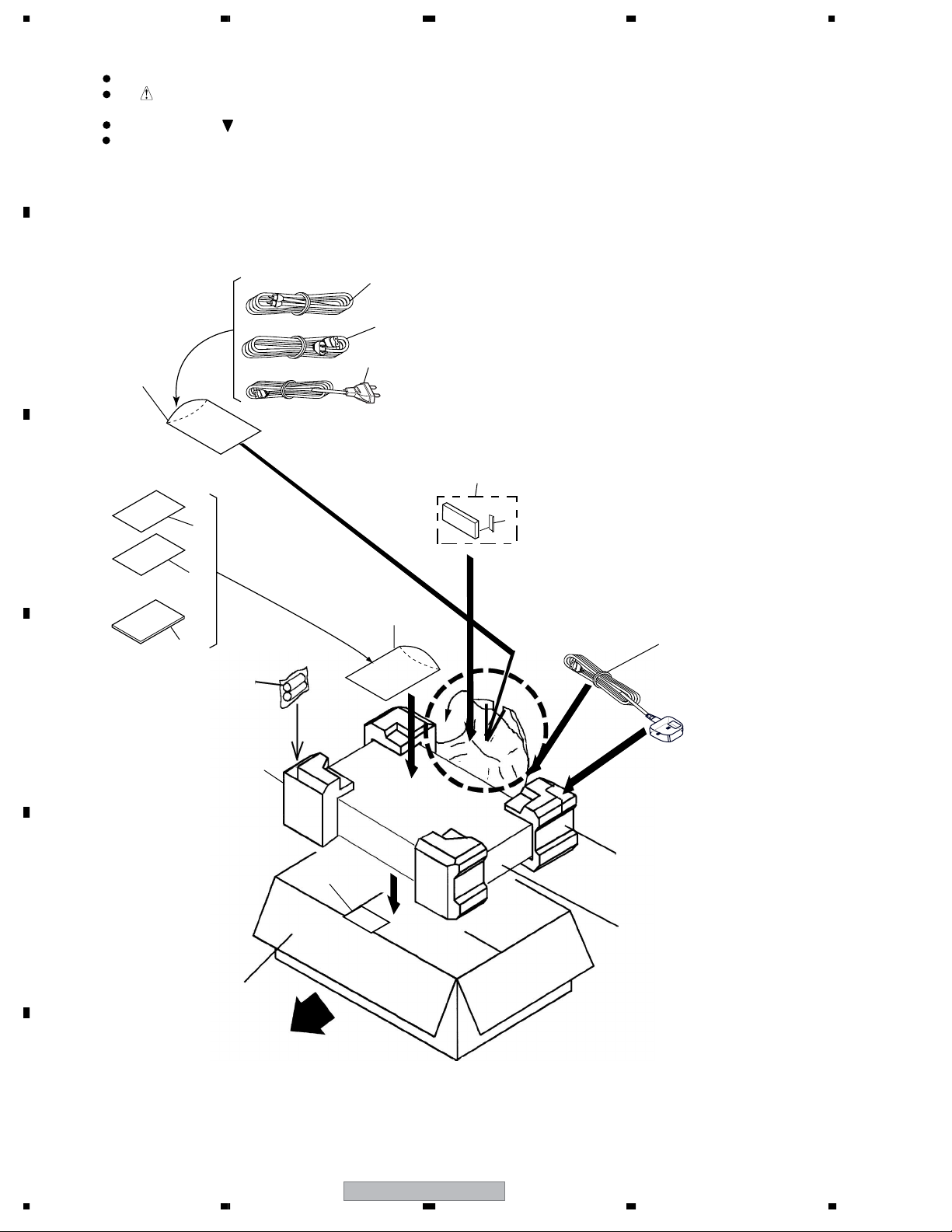
2. EXPLODED VIEWS AND PARTS LIST
NOTES:
A
Parts marked by "NSP" are generally unavailable because they are not in our Master Spare Parts List.
The mark found on some component parts indicates the importance of the safety factor of the part.
Therefore, when replacing, be sure to use parts of identical designation.
Screws adjacent to mark on product are used for disassembly.
For the applying amount of lubricants or glue, follow the instructions in this manual.
(In the case of no amount instructions, apply as you think it appropriate.)
2.1 PACKING SECTION
B
16
C
18
2
1
17
3
4
19
12
"Operating Instructions"
7-8
5
D
14
11
E
15
17
DV-686A-S
/WPWXTL Only
14
13
Front
F
6
1234
DV-686A-S
Page 7
>
>
>
>
5678
PACKING SECTION parts List
No. Description Part No.
Mark
1 Cord Set AC See Contrast Table(2)
2 Cord, RCA Pin 06CPBA2006
3 Remote Control VXX2914
4 Battery Cover VNK4998
NSP 5 Battery,Mangan (AR, R6P) 141L003010
No. Description Part No.
Mark
11 Package.Pad 792WHA0604
12 Polyethylene Bag, Instruction JB5KD200
13 Gift Sheet 791WHA0100
14 Package See Contrast Table(2)
15 Gift Box See Contrast Table(2)
A
6• • • •
7 Operating Instructions (English) J2G60901A
8 Operating Instructions(Chinese) See Contrast Table(2)
9• • • • •
10 • • • • •
NSP 16 Poly. Bag 791WHAA040
17 Cord Set AC See Contrast Table(2)
18 Sheet, FP Name See Contrast Table(2)
19 Remots Overlay See Contrast Table(2)
(2) CONTRAST TABLE
DV-686A-S/RLFXTL and DV-686A-S/WPWXTL are constructed the same except for the following :
Mark No. Symbol and Description DV-686A-S/RLFXTL DV-686A-S/WPWXTL
1 Cord Set AC 1206158802 Not used
8 Operating Instructions(Chinese) J2G60910A Not used
14 Package 792WHA0588 792WHA0597
15 Gift Box 793WCDC739 793WCDC795
17 Cord Set AC 120S198902 120G168801
18 Sheet, FP Name 723000D004 Not used
19 Remots Overlay VEC2406 Not used
B
C
D
E
F
56
DV-686A-S
7
7
8
Page 8
1234
2.2 EXTERIOR SECTION
A
20
14
NON-CONTACT
SIDE
CONTACT SIDE
B
PCB240
(POWER PCB ASS'Y)
4
19
9
19
C
19
F
19
A
11
20
Refer to
"2.3 05 DVD MECHA ASSY".
5
18
18
18
18
21
21
25
21
24
12
23
20
20
20
21
D
(OPERATION 3 PCB ASS'Y)
E
15
101D
F
" FRONT PANEL SECTION".
27
101E
101L
101
G
101K
17
101N
13
16
13
8
PCB280
22
(OPERATION 2 PCB ASS'Y)
3
C
101C
101G
101H
101B
101A
22
101M
101F
101I
16
7
26
101J
12
10
13
B
2
PCB270
(OPERATION PCB ASS'Y)
13
22
19
A
A
A
1
PCB130
(DVD PCB ASS'Y)
19
19
19
8
1234
DV-686A-S
Page 9
>
>
>
5678
EXTERIOR SECTION parts List
No. Description Part No.
Mark
1DVD MT PCB Assy A2G609A130
2 OPERATION PCB Assy A2G609A270
3 OPERATION 2 PCB Assy A2G501A280
4POWER PCB Assy A2G609A240
5DVD MECHA ASSY A2G512A650
6• • • •
7 PLATE, FIP 752WSA0466
NSP 8 Plate,Bottom 702WSA0252
9 Fuse (F501 : 1.6A) 080NT1R604
10 Sheet, Caution See Contrast Table(2)
11 Plate,Cover Power 755WPA0046
12 Holder,FFC 761WPA0396
13 Cushion, Leg VEB1349
14 Cabinet, Top 702WSB0114
NSP 15 Enargy Star Label See Contrast Table(2)
16 Cushion (15x20x16) 8965TS1015
NSP 17 POP Label 7236310006
18 Screw,Tap Tite(S)Bind Wash. 816423063U
19 Screw,Tap Tite(S) (3x5.5) 8107D3055U
20 Screw,Tap Tite(B) (3x6.0) 8109K3060U
21 Screw,Tap Tite(B)Pan (3x6) 810913060U
22 Screw,Tap Tite(P)Flat (2.6x10) 8110326A0U
No. Description Part No.
Mark
23 Sheet, Jack 1 7226310050
24 Sheet, Jack 2 See Contrast Table(2)
25 Sheet, Jack 3 See Contrast Table(2)
26 Double, Face-Tape 7290000156
27 OPERATION 3 PCB Assy A2G501ADF0
28 • • • •
101 Front Cabi Assy 7A701A434A
NSP 101A Cabinet,Front 701WPJD037
NSP 101B Plate,Display 711WPA0226
101C Flap,DVD 712WPD0182
101D Badge,Brand 7236310014
NSP 101E Button, Power 738WPB0052
NSP 101F Button,Cap 1 737WPB0003
NSP 101G Button,Frame 3 738WPA0142
NSP 101H Button,Frame 4 738WPB0053
NSP 101I Button,Frame 1 738WPA0132
NSP 101J Button,Frame 2 738WPA0133
101K Spring,Flap-DVD 743WKA0052
101L Plate, Cover 711WPD0682
NSP 101MButton, Cap 2 737WPB0004
NSP 101N Holder, Tag 761WPA0374
A
B
C
(2) CONTRAST TABLE
DV-686A-S/RLFXTL and DV-686A-S/WPWXTL are constructed the same except for the following :
Mark No. Symbol and Description DV-686A-S/RLFXTL DV-686A-S/WPWXTL
10 Sheet, Caution 726000A114 7260000356
NSP 15 Enargy Star Label Not used 7230007965
24 Sheet, Jack 2 722631A010 722631A057
25 Sheet, Jack 3 722631A011 722631A058
D
E
56
DV-686A-S
F
9
7
8
Page 10
1234
2.3 05 DVD MECHA SECTION
A
34
14
9
18
Cannot supply separately.
Lubricating Oil
GYA1001
AB
21
If the repair is needed, replace the
DVD MECHA ASS'Y.
15
B
Daifree
GEM1036
AB
11
AB
AB
AC
AB
C
AB
4
20
3
12
AC
AB
Lubricating Oil
GYA1001
23
19
29
6
CD2001
SW1
E
1
PCB610
5
AA
24
22
D
8
13
35
16
8
E
25
30
SW2
Note :
27
26
17
PCB640
(SW PCB ASS'Y)
22
2
32
31
10
Do not replace the parts. Because,
minute adjustments are needed if
this condition is disassembled
further more.
If the repair is needed, replace the
DVD MECHA ASS'Y.
D
(LOADING MOTOR PCB ASS'Y)
7
CD2302
28
33
CLASS
GREASE G-478B
F
PART NO.
GEM1018
GYA1001
PART NAME
GEM1036
CD2301
PN-397
ME-913A
MARK
AA
AB
AC
NOTE:
Applying positions AA, AB and AC for the
grease are displayed for this section.
Check if the correct grease is applied for each
position.
10
DV-686A-S
1234
Page 11

>
>
5678
05 DVD MECHA SECTION parts List
No. Description Part No.
Mark
1 Loading Motor PCB Assy A2F101A610
2 Gear,Middle 92P100117A
3 Loading Motor 1515S98004
4 Pulley,Motor 92P100097A
5 FEED Motor 1515S98004
6 Cord Jumper (24P)(CD2001) 122H002305
7 Cord Jumper (CD2302) 122H051602
8 Insulator (F) 92P200013A
9 Belt,Loading 92P200015A
10 Insulator (R) 92P200016A
A
11 Frame,main 92P100119A
12 Tray (B) 92P100127A
13 Holder ,Traverse 92P100125A
14 Gear,Pulley 92P100123A
15 Gear,Main 92P100124A
16 Gear,Feed 92P100116A
17 SW PCB Assy (PCB640) A2F101A640
18 Plate,Clamper 92P000023A
NSP 19 Loader SUB Assy 92AAA0019A
20 Clamper 92P100122A
21 Screw,Pan (M1.7x3 P3) 814011730U
22 Screw,Pan (M1.7x2.3 P3) 814011723U
23 Rack,Loading 92P100121A
24 Gear,Motor 92P100088A
25 Feed Rack Assy 92AAA0017A
26 Screw,T-Tite(B) (M1.7x5.0 P3) 813381750U
27 Screw,Gear Feed 92P700007A
28 Cord Jumper (CD2301) 122H061605
29 Switch (SW1) 0515S32003
30 Push Switch (SW2) 0500101036
31 Screw,Tap Tite(P) (2.6x8) 811022680U
32 Sems.Tap Tite(P) (2x8) 816112080U
33 Screw (Bind 2x8) 811022080U
>
34 DVD MECHA ASSY A2G512A650
NSP 35 Traverse SUB ASSY 92AAA0016A
B
C
D
56
DV-686A-S
E
F
11
7
8
Page 12
1234
3. BLOCK DIAGRAM AND SCHEMATIC DIAGRAM
3.1 BLOCK DIAGRAM
A
DVD MT PCB ASSY
A
DVD MECHA
ASSY
PICKUP
B
D
SW PCB ASSY
SPINDLE
M
MOTOR
SLED
M
MOTOR
C
E
LOADING MOTOR
PCB ASSY
LOADING
M
MOTOR
SW1
A
11 11
B
10 10
C
7 7
D
6 6
E
5 5
F
2 2
T+
21 21
T–
22 22
F+
23 23
F–
24 24
SP1+
6 1
SP1–
5 2
SLD+
4 3
SLD–
3 4
LD+
2 4
LD–
1 5
OPEN
3 3
CLOSE
5 1
CP2301
CP2303CD2301
CP2302CD2302
7
6
9
IC2301
8
Motor Drive
11
10
IC
51213 4
IC4004
16Mbit Flash
3
4
5
2
18
19
48
49
IC4005
64Mbit SDRAM
IC4002
MPEG / MICON
/ RF-AMP
1/6
A
228 229
X4001
(27MHz)
IC4001
EEPROM
219
218
217
225
194
196
203
200
202
198
ASDAT2
ASDAT1
ASDAT0
ASPDIF
S_Y
S_C
CR
Y
CB
CVBS
D
C
OPERATION 2
PCB ASSY
CP4002
10101111996
CP605
-28V
V+3E
FLDC–
FLDC+
E
CP604
6
V+3E
CP601
CP602CP603
Power
IC651
FIP Driver IC
V651 FL TUBE
30
F
OPERATION 3
G
PCB ASSY
OPERATION
B
PCB ASSY
12
DV-686A-S
1234
Page 13
A
4/6
IC8004 PCM1742KE
AUDIO DAC (C, Lfe)
ASDAT2
2
IC8005 PCM1742KE
AUDIO DAC (Ls, Rs)
ASDAT1
2
IC8003 PCM1742KE
AUDIO DAC (L, R)
16
1
ASDAT0
2
3
5678
A
AUDIO LPF & AMP
IC8006-1/2
BA4560F
VOUTL
7
VOUTR
8
VOUTL
7
A
VOUTR
8
VOUTL
7
VOUTR
8
2
3
6
5
2
3
6
5
2
3
6
5
8
1
7
IC8006-2/2
IC8007-1/2
BA4560F
8
1
7
IC8007-2/2
IC8008-1/2
BA4560F
8
1
7
IC8008-2/2
J8002
CENTER
SUB
WOOFER
J8002
L
R
J8001
L
R
L
R
SURROUND
FRONT
AUDIO
OUT (2 ch)
AUDIO
OUT
(5.1 ch)
B
V+1P8
(CORE)
A
6/6
IC4006
REG+1.8V IC
2 3
A
5/6
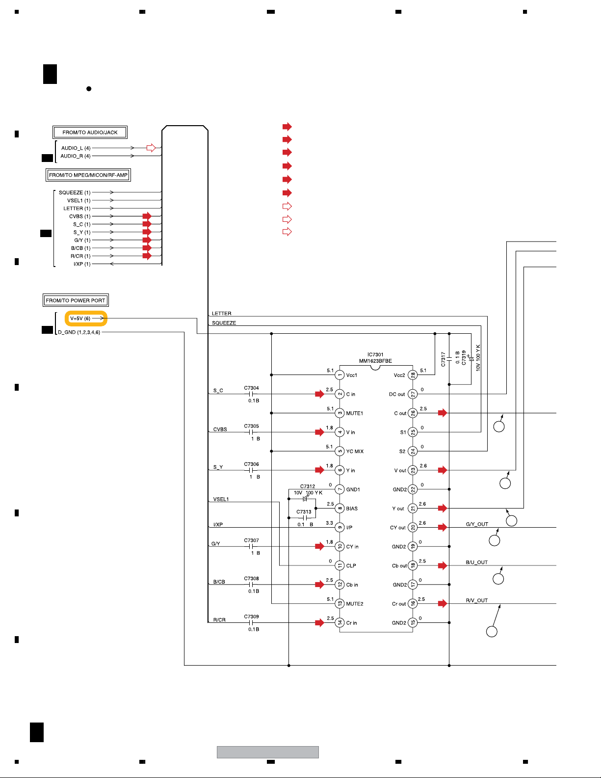
IC7301
Video Driver
6 ch
S_Y OUT
6
21
S_C OUT
2
26
14
10
12
CR out
16
Y out
20
CB out
18
V out
4
23
V+3
V+3A V+3E
(AUDIO VIDEO DAC)
(MPEG SDRAM FLASH)
(VIDEO OPT/COAX)
(AUDIO DAC)
V+5V V+5S
V+5A
(FLIP/LED/IR/RESET)
(OPU)
V+3F
(F/E)
V+6A
V+12AT
(MOTOR)
J7301
S VIDEO OUT
J7302
CR
Y
VIDEO
OUT
CB
CVBS
CP8001
(2P)
1 1
2 2
(AUDIO AMP)
V+12
(AUDIO MUTE)
2
3
5
6
8
9
12
13
14
P.CON+12V
AT+12V for MUTE
P.CON+5V
P.CON+6V
P.CON+3.3V
SPDIF
GND
AT+3.3V
FL DC–
FL DC+
-28V
CP8001
(2P)
CP502CP4003
POWER PCB ASSY
F
2
3
5
6
8
9
12
13
14
T501
Power Transformer
Q8103
F501
Fuse
J8004
DIGITAL OUT
COAXIAL
OS8101
OPTICAL
J501
L
AC IN
N
C
D
E
56
DV-686A-S
F
13
7
8
Page 14
1234
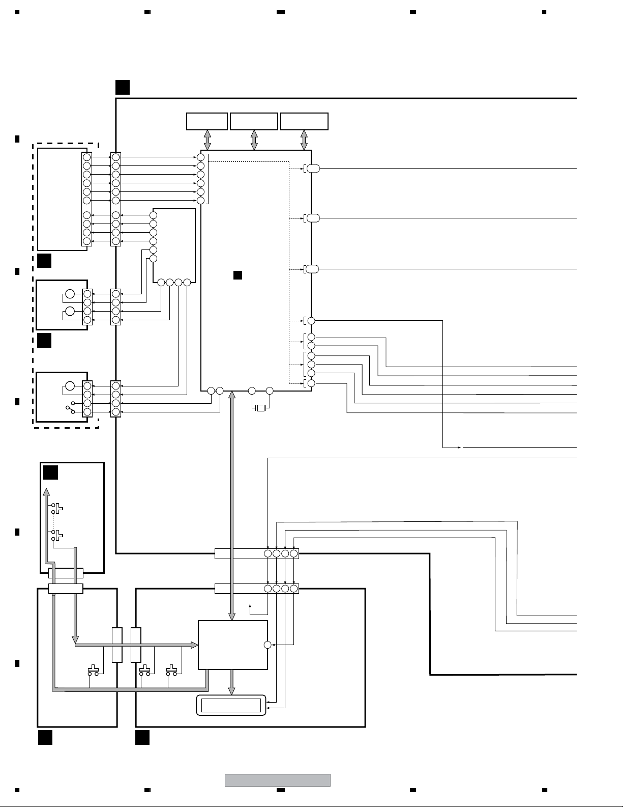
3.2 OVERALL WIRING CONNECTION DIAGRAM
A
DVD MECHA ASSY (A2G512A650)
CP2301
FF+
TT+
B
OPTICAL PICKUP
C
NC
GND(CD)
VOL(DVD)
GND(DVD)
LD(DVD)
GND(DVD)
VOL(CD)
MON(COM)
MON(DVD)
A
B
RF
DVD/CD(SW)
C
D
E
VCC
VREF
F
GND
24
23
22
21
20
19
18
17
16
15
14
13
12
11
10
9
8
7
6
5
4
3
2
1
24
23
22
21
20
19
18
17
16
15
14
13
12
11
10
9
8
7
6
5
4
3
2
1
24
23
22
21
20
19
LD_DVD(650)
18
17
16
15
14
13
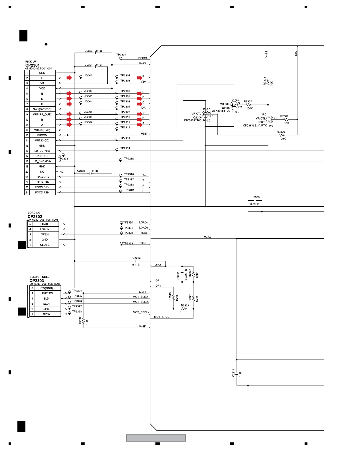
12
11
10
VRF(RF_OUT)
9
SW1(DVD/CD)
8
7
6
5
4
3
2
1
FOCS RTN
FOCS DRV
TRKG RIN
TRKG DRV
NC
GND
PD/GND
LD_CD(780)
GND
VR780(CD)
VRCOM
VR650(DVD)
A
B
C
D
E
VCC
VS
F
GND
D
E
F
14
SW PCB ASSY
D
(A2F101A640)
M2601
SPINDLE
JCV9B06
MOTOR
SW2
ESE22MH24
E
M2602
BCZ3B03
SLED MOTOR
LOADING MOTOR
PCB ASSY
(A2F101A610)
SW1
SSS-13-2
M2603
BCZ3B52
LOADING MOTOR
C
CP605
OPERATION 2
PCB ASSY
(A2G501A280)
D E
1234
M
M
M
CP604
069EV53050
069EV53050
5
5
SW2
4
4
PAUSE/–SKIP
3
3
PLAY/+SKIP
2
2
STOP
1
1
SW1
CD604(5P FFC)
122H051001
CD2301
2H062102
SPINDLE MOTOR (+)
SPINDLE MOTOR (-)
FEED MOTOR (+)
FEED MOTOR (-)
PICK UP INNER LIMIT SWITCH
LOADING MOTOR(+)
LOADING MOTOR(-)
GND(SW)
CD2302
2H052601
SW-2(CLOSE)
GND(SW)
SW-1(OPEN)
5
4
3
2
1
G
OPERATION 3
PCB ASSY
(A2G501ADF0)
6
5
4
3
2
1
FFC
1
2
3
4
5
6
069EV93050
PAUSE/–SKIP
DV-686A-S
CP2303
1
2
3
4
5
6
CP2302
1
2
3
4
5
CP603
IR
GND
V+3E
POWER
SW2
PLAY/+SKIP
STOP
SW1
SP1+
SP1SLD+
SLD-
LIMIT SW
SW(GND)
CLOSE
GND(D)
OPEN
LD+
LD-
1
1
2
2
3
3
4
4
5
5
6
6
77
898
9
CD603(9P FFC)
122H092801
CD601(11P FFC)
122H0B1002
CP602
069EV93050
9
8
8
9
7
7
6
6
5
5
4
4
PAUSE/–SKIP
PLAY/+SKIP
3
3
2
2
1
1
CP4002
069EVB3030
I R
GND
V+3E
POWER
SW2
STOP
SW1
CLK
STB
DI (M to F)
I R
V+ 3E
DO (F to M)
DGND
B
OPERATION
PCB ASSY
(A2G609A270)
987654321
1110
DGND
FL DC+
– 28V
FL DC –
987654321
1110
CP601
069EVB3050
Page 15
5678
÷
When ordering service parts, be sure to refer to "EXPLODED VIEWS and PARTS LIST" or
"PCB PARTS LIST".
÷
The > mark found on some component parts indicates the importance of the safety factor
A
of the part. Therefore, when replacing, be sure to use parts of identical designation.
÷
: The power supply is shown with the marked box.
A
A 1/6- A 6/6
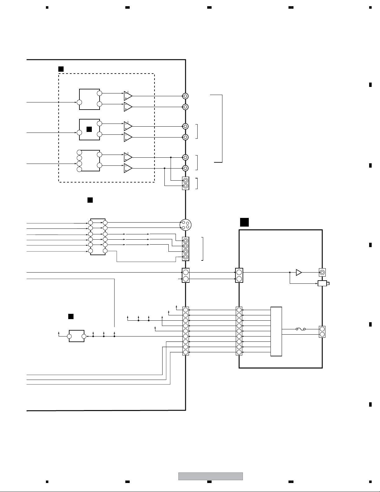
DVD MT PCB ASSY (A2G609A130)
: MPEG/MICON/RF-AMP BLOCK
A 1/6
: MEMORY BLOCK
A 2/6
: LOADER/MOTOR DRV BLOCK
A 3/6
: AUDIO JACK BLOCK
A 4/6
: VIDEO SEC BLOCK
A 5/6
: POWER PORT BLOCK
A 6/6
J8002
CENTER
SUB
WOOFER
J8002
L
R
J8001
L
R
J7302
CVBS
Y
Cb
Cr
J7301
Y
C
J8001
L
R
SURROUND
FRONT
VIDEO OUT
(COMPOSITE)
S VIDEO OUT
AUDIO OUT
AUDIO
OUT
(5.1 ch)
B
C
D
GND
CP4003
CP502(14P)
Cord Connector
06C32E3504
GND
P. CON+ 12V
069S2E0629
AT+12V for MUTE
3
2
1
3
2
1
3
2
1
3
2
1
CP502
GND
P. CON+ 12V
AT+12V for MUTE
P. CON+5V
5
4
5
4
5
4
GND
P. CON+5V
GND(M)
P. CON+6V
P. CON+3.3V(AT)
8
7
645
6
8
7
6
8
7
6
8
7
GND(M)
P. CON+6V
P. CON+3.3V
F
AT+3.3V
9
9
9
9
AT+3.3V
FL DC +
FL DC –
– 28V
GND(D)
STBY L
11
10
11
10
11
10
11
10
GND(D)
P. ON-H
13
12
13
12
13
12
13
12
FL DC +
FL DC –
14
14
14
14
– 28V
SPDIF
CP8001
A2001WV2-2P
1
1
1
1
SPDIF
CP8102
C3223003
F 1/2- F 2/2
GND2
2
2
2
GND
POWER PCB ASSY (A2G609A240)
: POWER BLOCK
F 1/2
: DIGITAL AUDIO BLOCK
F 2/2
56
DV-686A-S
E
J8102
J501
BLACK(L)
WHITE(N)
COAXIAL
OS8101
OPTICAL
BLACK
1
2
WHITE
DIGITAL
AUDIO
OUT
AC IN
F
15
7
8
Page 16
1234
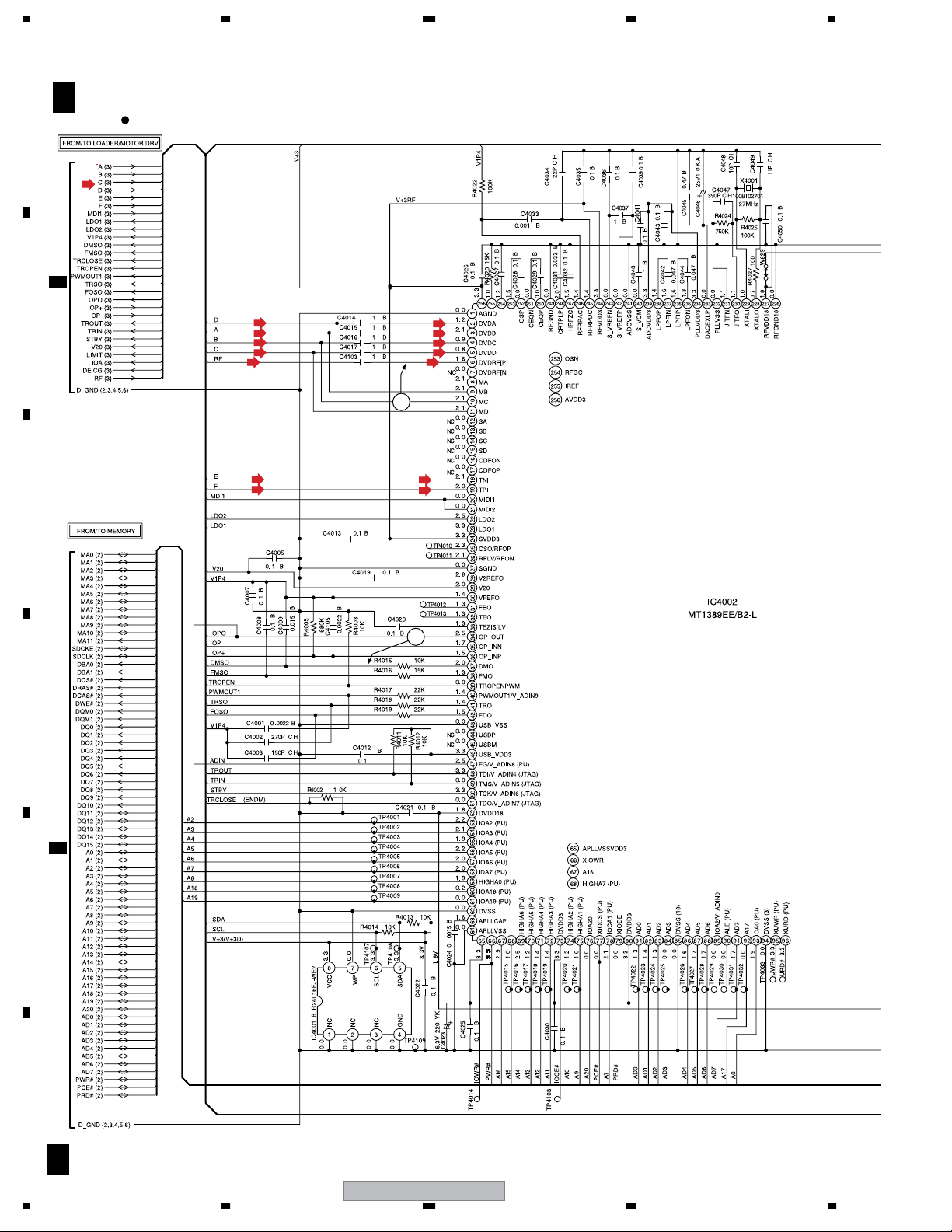
3.3 DVD MT PCB (1/6) ASSY
A
B
C
A 1/6
(RF)
3/6A2/6A
DVD MT PCB ASSY (A2G609A130)
MPEG/MICON/RF-AMP BLOCK
(D)
(A)
(B)
(C)
(RF) (RF)
1
(E)
(F)
(E)
(F)
(D)
(A)
(B)
(C)
17
D
E
EEPROM
MPEG/MICON
F
16
A 1/6
DV-686A-S
1234
Page 17
5678
A
(SY)
(SC)
(G/Y)
(B/CB)
(R/CR)
(D)
(DA)
(R/CR)
(B/CB)
(G/Y)
(SC)
5/6A
(SY)
B
(RF)
: RF SIGNAL ROUTE
: VIDEO SIGNAL ROUTE
(SY)
: S VIDEO SIGNAL ROUTE (Y ch)
(SC)
: S VIDEO SIGNAL ROUTE (C ch)
(R/CR)
: VIDEO SIGNAL ROUTE (R/CR ch)
(G/Y)
: VIDEO SIGNAL ROUTE (G/Y ch)
(B/CB)
: VIDEO SIGNAL ROUTE (B/CB ch)
(D)
: AUDIO DATA SIGNAL ROUTE
(DA)
: AUDIO SIGNAL ROUTE (Digital)
(DA)
(D)
4/6A
C
6/6A
D
RESET IC
DV-686A-S
56
E
CP601
B
F
A 1/6
17
7
8
Page 18
1234
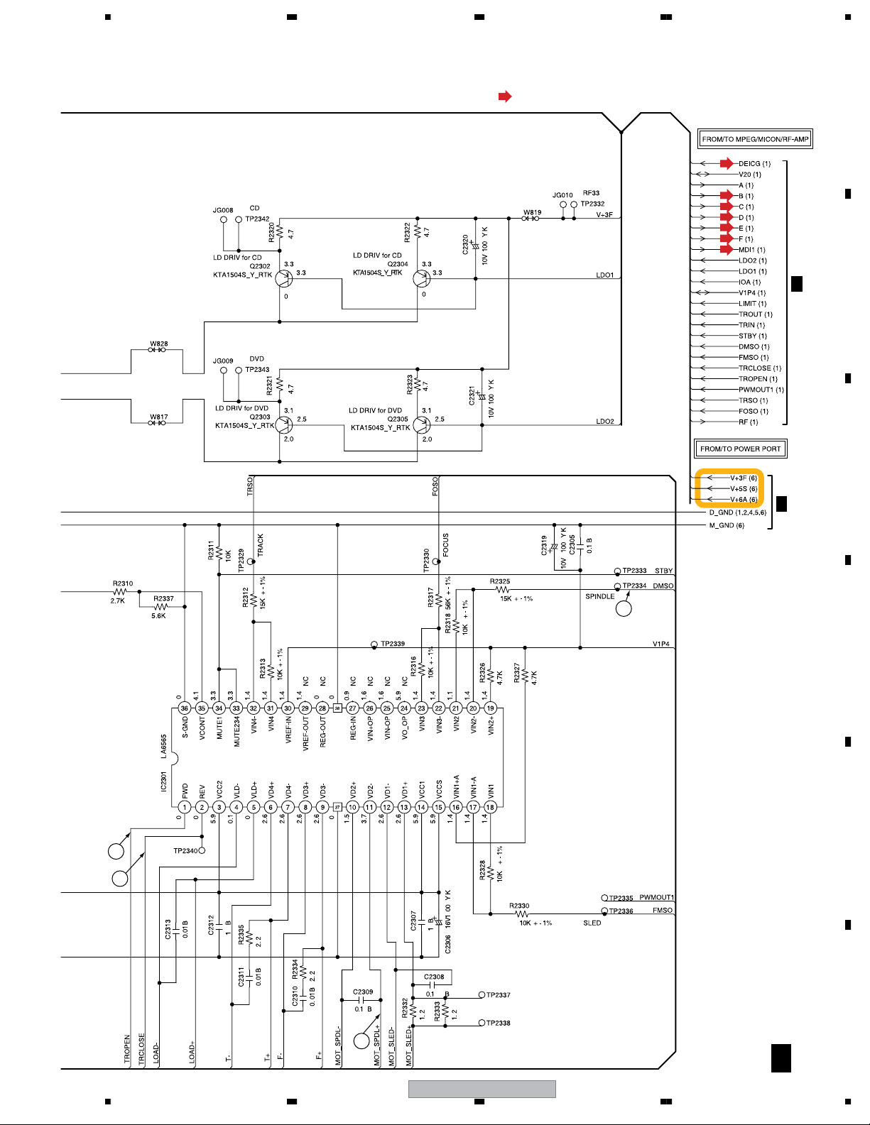
3.4 DVD MT PCB (2/6) ASSY
A
B
C
A 2/6
DVD MT PCB ASSY (A2G609A130)
MEMORY BLOCK
1/6A
D
E
F
18
A 2/6
1/6A
6/6
A
NOTE : THE DC VOLTAGE EACH PART WAS
MEASURED WITH THE DIGITAL TESTER
DURING PLAYBACK.
DV-686A-S
1234
NOTE : THIS SCHEMATIC DIAGRAM IS THE LATEST
AT THE TIME OF PRINTING AND SUBJECT TO
CHANGE WITHOUT NOTICE
Page 19
5678
A
64Mbit SDRAM
16Mbit FLASH
B
C
D
E
56
DV-686A-S
F
A 2/6
19
7
8
Page 20
1234
3.5 DVD MT PCB (3/6) ASSY
A
B
C
A 3/6
DVD MT PCB ASSY (A2G609A130)
To PICKUP
LOADER/MOTOR DRV BLOCK
(F)
(E)
(D)
(C)
(RF)
(B)
(A)
(F)
(E)
(D)
(C)
(RF)
(B)
(A)
D
E
F
CD2302
E
CD2301
D
NOTE : THE DC VOLTAGE EACH PART WAS
MEASURED WITH THE DIGITAL TESTER
DURING PLAYBACK.
NOTE : THIS SCHEMATIC DIAGRAM IS THE LATEST
AT THE TIME OF PRINTING AND SUBJECT TO
CHANGE WITHOUT NOTICE
A 3/6
20
DV-686A-S
1234
Page 21
5678
(RF)
: RF SIGNAL ROUTE
(RF)
(A)
(B)
(C)
(D)
(E)
(F)
A
B
1/6A
15
C
6/6A
17
D
MOTOR DRIVE IC
E
16
18
DV-686A-S
56
F
A 3/6
21
7
8
Page 22
1234
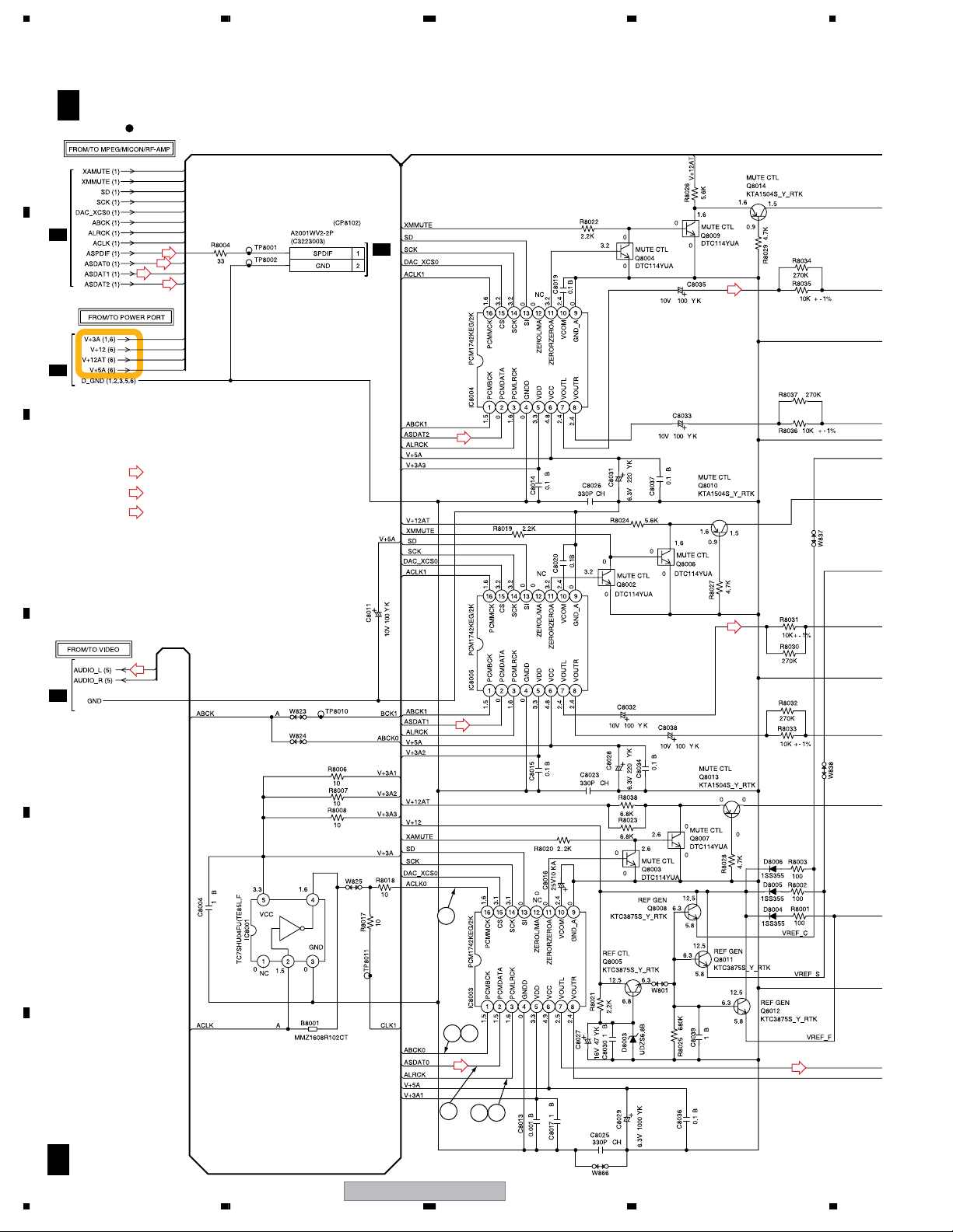
3.6 DVD MT PCB (4/6) ASSY
A
B
C
A 4/6
1/6A
6/6A5/6A
DVD MT PCB ASSY (A2G609A130)
AUDIO JACK BLOCK
CP8001
(DA)
(D)
(D)
(D)
(D)
: AUDIO DATA SIGNAL ROUTE
(DA)
: AUDIO SIGNAL ROUTE (Digital)
: AUDIO SIGNAL ROUTE (L ch)
2/2F
AUDIO DAC (C,Lfe)AUDIO DAC (Ls,Rs)
(D)
(DA)
D
E
INVERTER
(D)
3
AUDIO DAC (L,R)
4 7
(D)
F
22
A 4/6
8
6
5
DV-686A-S
1234
Page 23
5678
A
NOTE : THE DC VOLTAGE EACH PART WAS
MEASURED WITH THE DIGITAL TESTER
DURING PLAYBACK.
AUDIO LPF&
AUDIO LPF&
B
C
D
AUDIO LPF&
DV-686A-S
56
E
F
A 4/6
23
7
8
Page 24
1234
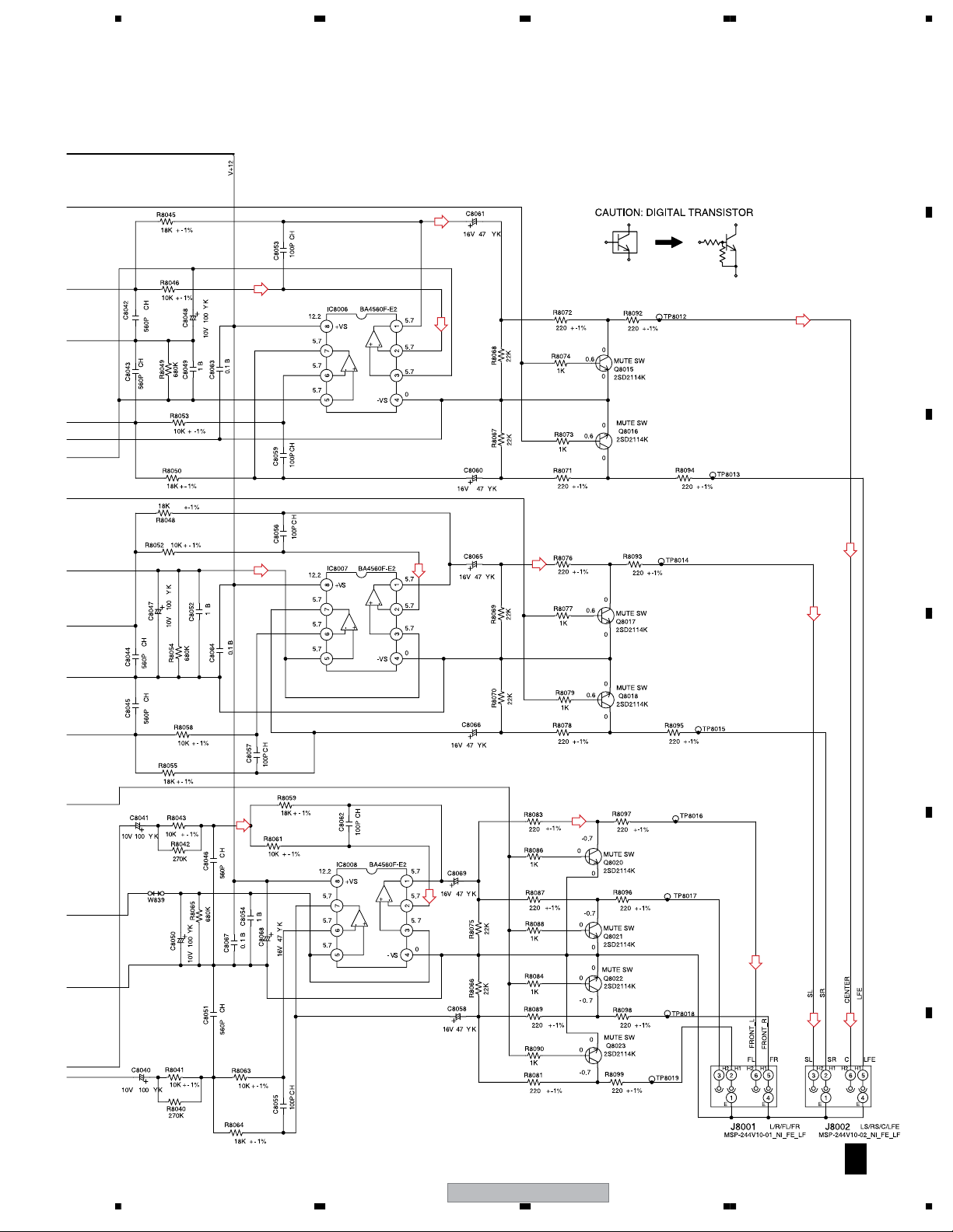
3.7 DVD MT PCB (5/6) ASSY
A
A 5/6
DVD MT PCB ASSY (A2G609A130)
VIDEO SEC BLOCK
: VIDEO SIGNAL ROUTE
(SY)
(DA)
B
1/6A
C
6/6A 4/6A
(SC)
(SY)
(Y)
(CB)
(CR)
: S VIDEO SIGNAL ROUTE (Y ch)
(SC)
: S VIDEO SIGNAL ROUTE (C ch)
(CR)
: VIDEO SIGNAL ROUTE (CR ch)
(Y)
: VIDEO SIGNAL ROUTE (Y ch)
(CB)
: VIDEO SIGNAL ROUTE (CB ch)
(D)
: AUDIO DATA SIGNAL ROUTE
(DA)
: AUDIO SIGNAL ROUTE (Digital)
: AUDIO SIGNAL ROUTE (L ch)
VIDEO DRIVER 6CH
(SC)
(SC)
14
D
(SY)
9
(SY)
(Y)
E
(CB)
(CR)
(Y)
(CB)
(CR)
13
10
11
12
F
24
A 5/6
DV-686A-S
1234
Page 25
5678
A
NOTE : THE DC VOLTAGE EACH PART WAS
MEASURED WITH THE DIGITAL TESTER
DURING PLAYBACK.
B
(SY)
(CB)
C
(Y)
(CB)
(SC)
(CR)
(Y)
J7301
(SY)
(CR)
(CB)
CB
CR
(CR)
(SC)
(Y)
D
E
J7302
DV-686A-S
56
F
A 5/6
25
7
8
Page 26

1234
3.8 DVD MT PCB (6/6) ASSY
A
A 6/6
B
C
DVD MT PCB ASSY (A2G609A130)
POWER PORT BLOCK
REG+1.8V IC
D
CP502
F 1/2
E
F
A 6/6
26
DV-686A-S
1234
Page 27

5678
A
4/6A
B
5/6A
NOTE : THE DC VOLTAGE EACH PART WAS
MEASURED WITH THE DIGITAL TESTER
DURING PLAYBACK.
3/6
C
A
1/6A
D
E
56
DV-686A-S
F
A 6/6
27
7
8
Page 28

1234
3.9 OPERATION, OPERATION 2 and OPERATION 3 PCB ASSYS
A
B
OPERATION 2
PCB ASSY
C
SW660 : STOP
SW662 : +SKIP
SW664 : - SKIP
SW663 : PLAY
SW665 : PAUSE
OPERATION PCB ASSY
SW652 : DOWN
SW653 : ENTER
SW654 : RIGHT
SW655 : RETURN
SW656 : MENU
SW657 : UP
SW658 : TOPMENU
SW659 : LEFT
SW661 : HOMEMNU
OPERATION 2 PCB ASSY
C
(A2G501A280)
B
OPERATION PCB ASSY
(A2G609A270)
CP605
D
OPERATION 3 PCB ASSY
G
(A2G501ADF0)
E
OPERATION 3 PCB ASSY
SW667 : POWER
F
CP604
CP603
CP602
B C G
28
DV-686A-S
1234
Page 29

5678
A
B
FIP DRIVER IC
C
D
CP601
E
NOTE : THE DC VOLTAGE EACH PART WAS
MEASURED WITH THE DIGITAL TESTER
DURING PLAYBACK.
NOTE : THIS SCHEMATIC DIAGRAM IS THE LATEST
AT THE TIME OF PRINTING AND SUBJECT TO
CHANGE WITHOUT NOTICE
56
DV-686A-S
A 1/6
CP4002
F
B
29
7
8
Page 30

1234
3.10 POWER PCB (1/2) ASSY
A
B
C
F 1/2
POWER PCB ASSY (A2G609A240)
POWER BLOCK
J501
•
•
D
PHOTO
E
COUPLER
• NOTE FOR FUSE REPLACEMENT
CAUTION -
FOR CONTINUED PROTECTION AGAINST RISK OF FIRE.
REPLACE WITH SAME TYPE AND RATINGS OF FUSE.
F
F 1/2
30
DV-686A-S
1234
Page 31

5678
A
6V REG
(DVD MOTOR)
B
CP4003
A 6/6
C
2/2F
D
VOLTAGE
CTL
NOTE : THE DC VOLTAGE EACH PART WAS
MEASURED WITH THE DIGITAL TESTER
DURING PLAYBACK.
DV-686A-S
56
E
F
F 1/2
31
7
8
Page 32

1234
3.11 POWER PCB (2/2) ASSY
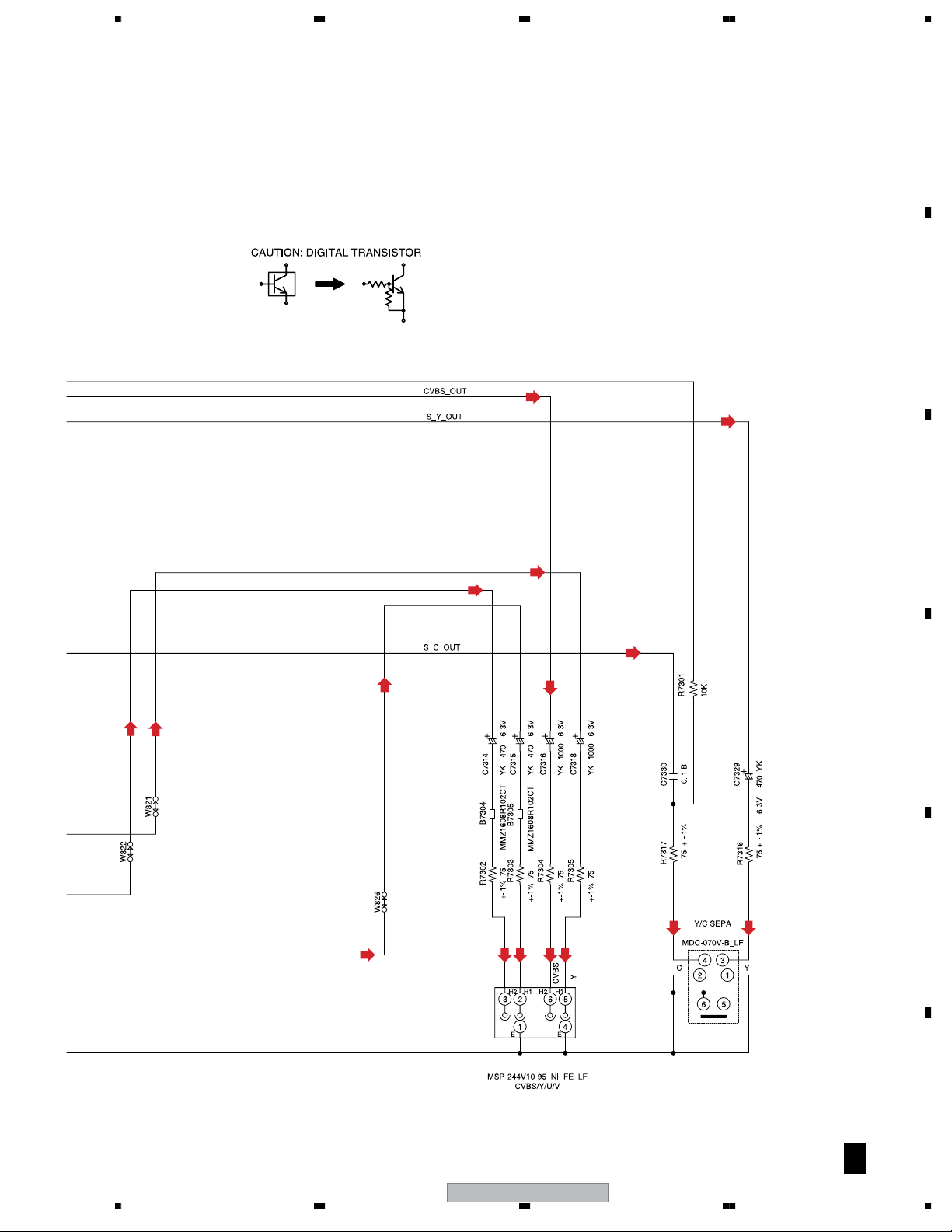
A
B
C
F 2/2
POWER PCB ASSY (A2G609A240)
DIGITAL AUDIO BLOCK
: AUDIO SIGNAL ROUTE (L ch)
(DA)
: AUDIO SIGNAL ROUTE (Digital)
FROM/TO POWER
P.CON+D5V {1}
D
E
1/2F
MMZ1608R102CT
F
32
F 2/2
DV-686A-S
1234
Page 33

5678
4/6A
CP8102
C3223003
1
2
SPDIF
GND
TP8101
TP8102
(DA)
ASPDIF
(DA)
R8106
2.2K
R8107
2.7
R8121
1.8K
4.9
COAXIAL DRV
Q8103
2.1
KTC3875S_Y_RTK
+-1%
3.9K
220
R8122
(DA)
W802
R8123
68
COAXIAL
CH
C8103
C8104
100P
C8120
150V KA
J8102
0.1 B
100K
R8124
COAXIAL
H
2
YLC21-3055N
OS8101
(DA)
C8118
10010V YK
C8119
1B
W801
E
1
OPTICAL
OFTG038101
1
INPUT
2
VCC
3
GND
A
(DA)
B
C
D_GND
CAUTION: DIGITAL TRANSISTOR
NOTE : THE DC VOLTAGE EACH PART WAS
CAUTION: DIGITAL TRANSISTOR
MEASURED WITH THE DIGITAL TESTER
DURING PLAYBACK.
D
E
F
56
DV-686A-S
F 2/2
33
7
8
Page 34

1234
3.12 WAVEFORMS
Note : The encircled numbers denote measuring point in the schematic diagram.
A
Measurement condition
No. 3 to 8 : reference A1 (DVD), T2-chp 1
DVD MT PCB ASSY
A
: No. 1 to 2 and 9 to 14 : reference A1 (DVD), T2-chp 19, Color-bar
Foot of C626 [RF](IC4002 - pin 6)
1
V: 200mV/div. H: 0.1µsec/div.
Foot of R8070 (IC8003 - pin 16)
3
[AUDIO DAC -MCLK]
B
GND
C
Foot of R4004 (IC8003 - pin 1)
4
[AUDIO DAC -BCK]
V: 2V/div. H: 200nsec/div.
D
E
Foot of R4050 (IC8003 - pin 3)
5
[AUDIO DAC -LRCK]
V: 2V/div. H: 5µsec/div.
(IC7301 - pin 20)
10
[Component Video out -Y]
V: 1V/div. H: 10µsec/div.
(IC7301 - pin 18)
11
[Component Video out -Pb]
V: 2V/div. H: 10µsec/div.
(IC7301 - pin 16)
12
[Component Video out -Pr]
V: 2V/div. H: 10µsec/div.
Foot of R4050 (IC8003 - pin 3)
6
[AUDIO DAC -LRCK]
Foot of R8047 (IC8003 - pin 1)
7
[AUDIO DAC -BCK]
Foot of R4043 (IC8003 - pin 2)
8
[AUDIO DAC -DATA]
(Waveform of DATA is unsettled.)
6
7
8
V: 2V/div. H: 500nsec/div.
(IC7301 - pin 21)
13
[S Video out -Y]
V: 1V/div. H: 10µsec/div.
10
11
12
(IC7301 - pin 26)
14
[S Video out -C]
V: 1V/div. H: 10µsec/div.
(IC7301 - pin 23)
9
[Composite Video out]
V: 1V/div. H: 10µsec/div.
13
14
F
34
DV-686A-S
1234
Page 35

5678
DVD MT PCB ASSY
A
A
Foot of R4026(IC2301 - pin 1) [TROPEN]
15
Foot of R618 (IC4002 - pin 37) [DMSO]
17
[Tray is Open]
15
16
Foot of R4002(IC2301 - pin 2 [TRCLOSE]
16
[Tray is closing]
V: 1V/div. H: 5µsec/div.V: 1V/div. H: 5µsec/div.
[DMSO_PLAY][DMSO_OPEN] [DMS~3]
15
16
OPEN KEY ON
Tray:
opening
PLAY
Braking a turn of disc
PLAY KEY ON:
starting a turn of disc
B
C
CN2303 - pin 1
18
(IC2301 - pin 11)
[MOT_SPDL+]
V: 1V/div. H: 10µsec/div.
V: 2V/div. H: 2msec/div.
V: 1V/div. H: 10µsec/div.
V: 1V/div. H: 2sec/div.
D
E
56
DV-686A-S
F
35
7
8
Page 36

1234
A
B
C
D
E
F
36
1234
DV-686A-S
Page 37

5678
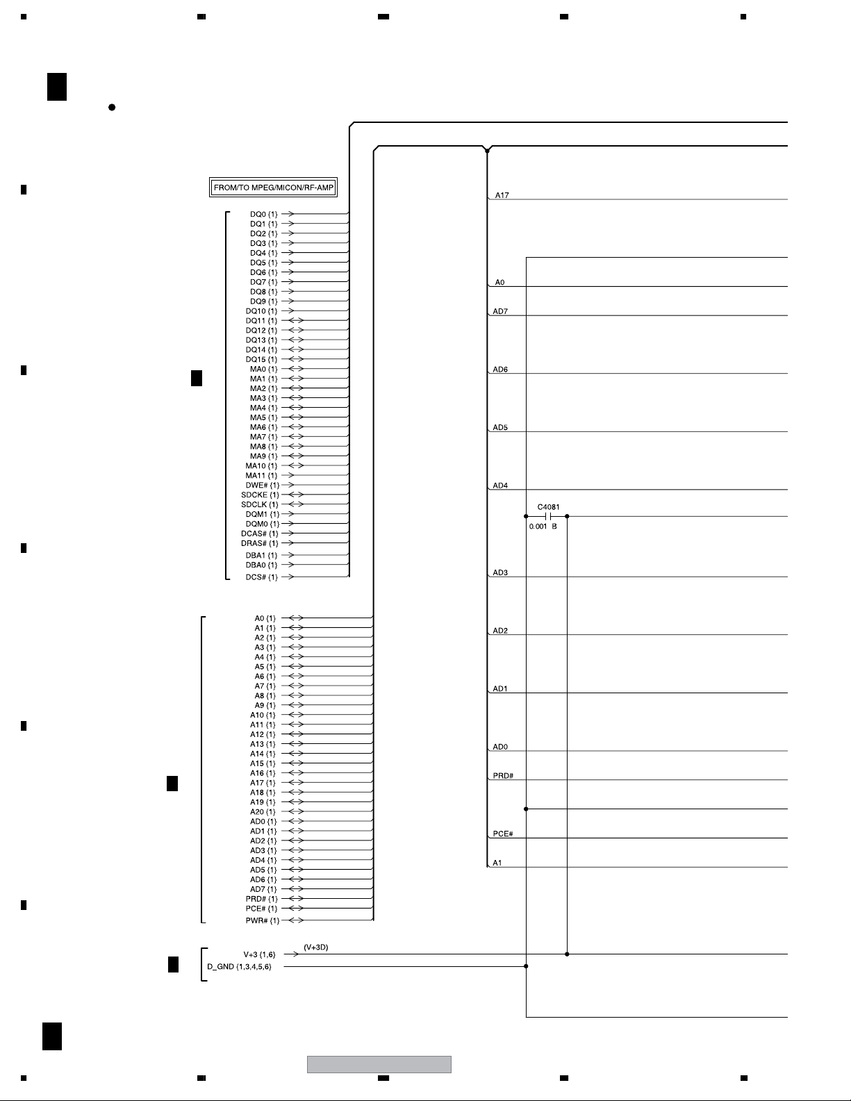
4. PCB CONNECTION DIAGRAM
4.1 LOADING and SW PCB ASSYS
NOTE FOR PCB DIAGRAMS :
1. Part numbers in PCB diagrams match those in the schematic
diagrams.
2. A comparison between the main parts of PCB and schematic
diagrams is shown below.
Symbol In PCB
Diagrams
BCE
BCE
D
Symbol In Schematic
Diagrams
BCEBCE
BCE
DGGSS
LOADING MOTOR
E
BCE
DGS
Part Name
Transistor
Transistor
with resistor
Field effect
transistor
Resistor array
3-terminal
regulator
PCB ASSY
(INSERTED PARTS)
3. The parts mounted on this PCB include all necessary parts for
several destinations.
For further information for respective destinations, be sure to
check with the schematic diagram.
4. View point of PCB diagrams.
Connector
Capacitor
SIDE A
P.C.Board
LOADING MOTOR
E
Chip Part
SIDE B
PCB ASSY
(CHIP MOUNTED PARTS)
A
B
C
SIDE A SIDE B
SW1
CD2302
A
CP2302
M2603
LOADING MOTOR
SW PCB ASSY
D
SW2
D
E
M2602
SLED
MOTOR
A
CP2303
CD2301
7
D
8
CD2301
M2601
SPINDLE
E
D E
56
MOTOR
DV-686A-S
F
37
Page 38

1234
5
R4027
0
0
9
R4001
5
0
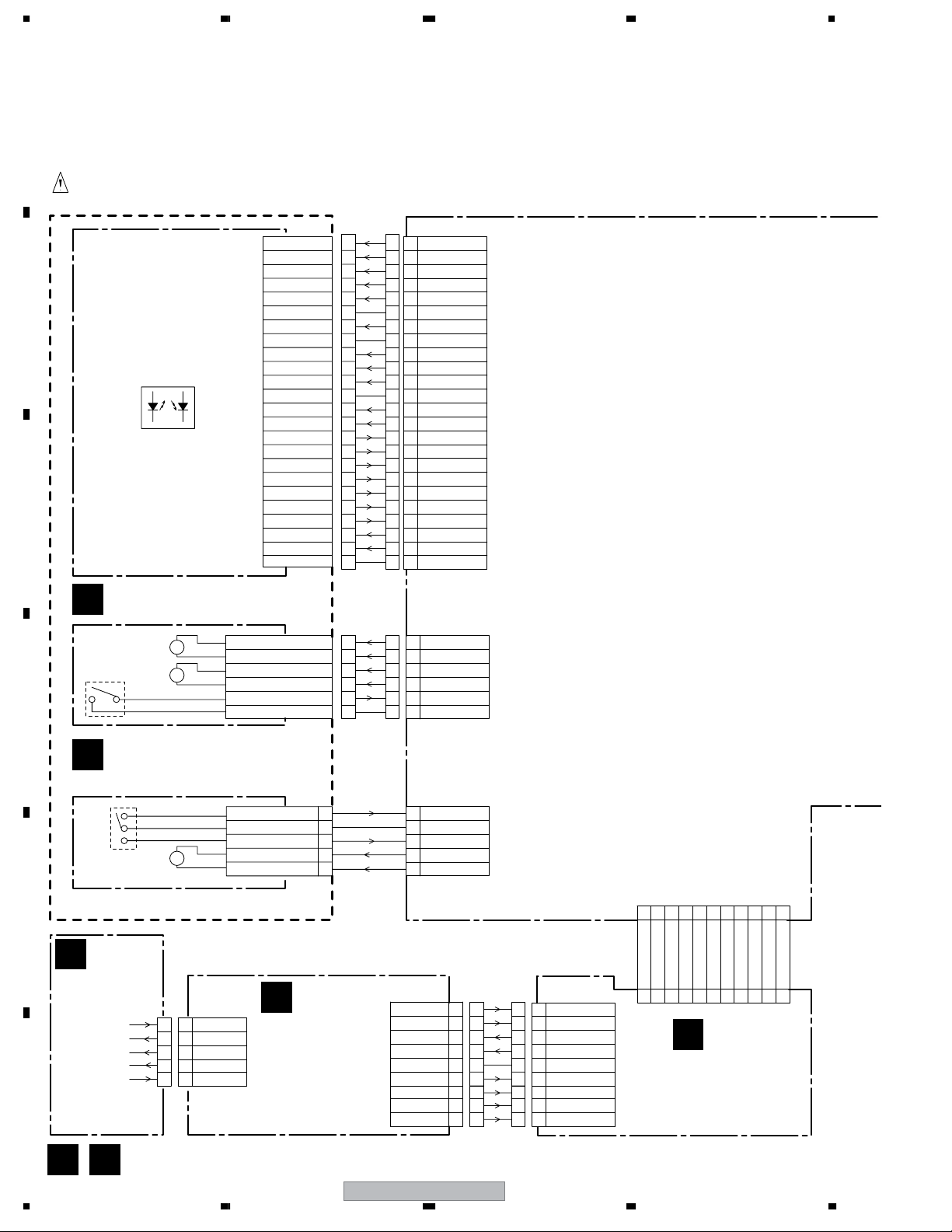
4.2 DVD MT PCB ASSY
A
SIDE A
DVD MT PCB ASSY
A
CP503
F
CP8001
F
CP40
CP
B8001
R4024
C4044
C4042
C4041
R4069
R4064
C8017
R4040
R4038
W829
C4050
C4048 C4049
C4047
R4068
R4067
R4066
C8025
R8006
C4040
C4039
C4036
C7312
W814
R4065
B4002
R4048
R4050
R4047
R4046
X4001
C4046
W816
W811
W812
W815
W813
R4043
C4035
W848
C4102
C4037
C40
C40
R4
R4
R4025
C4033
R4022
W847
C4
C4
C8030
IC8008
R8061
C8062
R8059
R8058
IC8007
C8056
R8052
R8048
R8050
C8059
R8053
IC8006
C8053
R8046
SPDIF
C7318
R8064
C8051
C8046
R8055
C8045
C8044
C8042 C8043
R8045
W821
Q8005
R8021
R8065
C8052
R8054
C8049
R8049
W801
W839
R8001
D8004
C8054
R8020
R8030
R8031
R8036
R8037
W826
W822
R7317
R8040
R8041
R8042
R8032
D8006
R8034
Q8012
R8043
C8016
R8033
R8003
W837
R8035
C7330
R7301
R8025
C8039
C8040
C8041
C8047
C8038
C8032
C8048
C8033
C8035
C4116
C8011
Q8011
Q8008
C8036
W838
Q8014
C8050
C8013
IC8003
C8028
C8034 C8015
IC8005
C8020
C8031
C8037
IC8004
C8019
Q8004
Q8009
R8022
R8026
C7317
W866
R8096
R8097
R8095
R8094
R8092
R8090
R8088
R8084
R8086
R8079
R8077
R8073
R8074
B7304
R7304
R7316
R8081R8099
Q8023
R8087
R8089R8098
Q8022
R8083
R8078
R8076R8093
Q8016
R8072
B7305
R7303
R7305
Q8021
Q8020
Q8018
Q8017
Q8015
R7302
R8066
R8028
Q8010
R8071
C7329
C8058
R8075
Q8013
R8070
R8069
R8027
R8068 R8067
C7314
C7316
B
J8001J8002
C
D
J7302
E
J7301
C8069
C8066
C8065
R8024
C8060
C8061
C7315
D8003
C8068
Q8007
Q8006
C8027
R8063
C8055
C8067
Q8003
R8023
R8038
C8057
C8064
Q8002
R8019
C8063
R8004
CP8001
GND
C8014
R8029
D8005
R8018
C8023
R8007
C8026
IC7301
W824
R8008
R8002
C8029
C8004
W823
C7319
W825
IC8001
R8017
C4045
C4043
C7309
C7308
C7307
C7313
C7306
C7305
C7304
P.CON+5V
GND
AT+12V for MUTE
P.CON+12V
GND
F
Q8023-Q8020
Q8017-Q8018 Q8014
Q8010
Q8015-Q8016
Q8013
Q8007
Q8006
Q8002
IC8008
IC8007
IC8006
Q8005
Q8008Q8003
IC8012
IC8002
Q8011
A
38
DV-686A-S
IC8005
Q8004
IC8003
IC8004
Q8009
IC7301
1234
Page 39

5678
IC8001
A
CP502
F
SIDE A
CP4003
R4071
R4070
C4012
R4002
R4015
C4001
R4016
C4007
C2321
R2323
R2306
Q2307Q2306
CP2301
C4021
Q2305
R2321
C4088
NR4002
R4018
R4017
C4008
C4009
C2320
R2322
Q2303
129193
W819
C4024
C2314
C2306
R2320
C2301
C4023
Q2304
Q2302
W817
C4064
R4019
C4002
C4003
B
C4084
C4022
IC4001
R4051
C4062
C4030
C4025
R4087
W820
C4105
R4005
R4012
R4011
R2328
C2307
R2330
R2316
R2326
R2327
R2318
R2317
R2325
CP2303
W828
SPD-
SPD+
SLD+
SLD-
NR4001
C2325
IC2301
LIMIT SW
SW(GND)
R4007
C4054
R4013
R4014
R4036
IC4004
C2313
R2338
C4086
C4076
C4081
R4003
R2313
C2305
C4077
B4008
C2312
R2312
C4104
C4114
R2311
C4078
R2337
R2310
R2335
C2311
C4091
C2319
IC4003
2
0
0
4
P
C
CLOSE
0
3
2
P
C
C2308
R4084
C4079
R4035
LOAD+
OPEN
GND
2
R2332
R2333
F
LOAD-
C2323
C2322
R2342
R2331
R2319
R2329
C2309
DC-
DC+
F to
28V
DGND
DGND
(
M to
CLK
C2310
R2334
L
F
-
L
F
B
CP4002
CP601
V+3E
IR
M)
DO
STB
)
(
DI
C
E
CP2302
CD2302
D
D
CP2303
CD2301
E
PICKUP
CP2301
C8025
002
9
R8006
C8017
W825
4
C4045
C4043
7309
7308
7307
C7313
C7306
7305
C7304
7319
B8001
R4024
C4044
C4042
C4041
R4040
R4038
W829
C4050
C4048 C4049
C4047
R4069
R4068
R4067
R4064
R4066
C4040
C4039
C4036
C7312
W814
R4065
B4002
R4048
R4050
R4047
R4046
X4001
C4046
W816
W811
W812
W815
W813
R4043
C4035
W848
C4102
R4052
R4054
C4053
R4025
C4037
C4099
C4098
C4093
W847
R4027
C4033
C4032
C4034
R4022
R4001
C4066
R4030
C4029
C4027
C4031
R4033
C4111
W804
R4062
R4061
C4061
C4060
C4028
C4026
R4020
C4100
C4052
R4008
R4006
C4109
C4063
C4014
B4001
IC4006
C4085
IC4005
W806
W807
C4068
C4110
C4071
C4067
C4117
R4082
IC4002
C4082
R4083
C4072
C4073
165
C4013
C4020
C2302
C4095
C4019
C4005
C4103
R2309
Q2301
R2308
R2307
C2303
R4044
C4015
C4096
C4101
C4017
C4016
W852
W851
W865
C4094
W850
CP4003
GND
IC4006
IC4005
Q2306
IC4002
Q2307
Q2305
Q2303
VCCVSFGN D
SW1(DV D/ CD)
CDE
Q2302
Q2304
VRF(RF _O UT )
VR78 0( CD)
V RCO M
VR65 0( DV D)AB
IC2301
GN D
LD_ D V D( 650)
PD / GN D
LD_ CD( 7 80)
GN D
IC4004
FOCS RT N
FOCS DRV
TR K G R T N
TRKG DRV
NC
F
-28V
FL DC+
FL DC-
GND(D)
STBY L
AT+3.3V
P.CON+3.3V
GND(M)
P.CON+6V
P.CON+5V
GND
AT+12V for MUTE
P.CON+12V
Q2301
A
56
DV-686A-S
7
8
39
Page 40

A
B
SIDE B
1234
DVD MT PCB ASSY
A
C
D
CP2302 CP4002
E
F
CP2303
CP2301
CP4003
A
40
1234
DV-686A-S
Page 41

5678
SIDE B
A
B
C
D
E
CP8001
DV-686A-S
56
F
A
41
7
8
Page 42

1234
W
T
A
4.3 OPERATION, OPERATION 2 and OPERATION 3 PCB ASSYS
SIDE A
A
OPERATION 3 PCB ASSY
G
POWER
DIP
2
CP603
NTSC
8
DEE039A3
B
SW667
9
CP603
OPERATION PCB ASSY
B
C
RETURN
SW655
SW654
RIGHT
SW656
D
MENU
DOWN
SW652
SW653
ENTER
SW657
UP
CP601
11
W001
SW661
HOMEMENU
SW659
LEFT
TOPMENU
W002
SW658
10
W004
NTSC
W003
DEE028
2
D663
15
W005
D667
E
F
B C G
42
CP601
CP4002
A
OPERATION 2 PCB ASSY
C
2
SW664
CP605
- SKIP
CP605
CP604
G
DV-686A-S
1234
4
SW662
5
+ SKIP
DEE038A
3
S
S
Page 43

5678
SIDE A
A
TSC
039A
EE028A
W005
D667
OS651
C674
R666
2
CP604
4
5
B
CP604
CP605
C
CP602
3
W008
W007
W006
8
D651
D652
D654
D655
D656
D657
D658
D659
9
2
CP602
W805
EJECT
SW666
C
D
52832
V651
SW665SW660
NTSC
PAUSESTOP
SW663
PLAY
DV-686A-S
56
E
F
CB G
43
7
8
Page 44

A
D
B
SIDE B
1234
OPERATION 3 PCB ASSY
G
C651
CP604
OPERATION PCB ASSY
B
C
R658
C609
D
R656
R651
R655
R657
C676
R654
R662
R652
R653
12
C675
1
IC651
34
23
CP601
IC651
E
OPERATION 2 PCB ASSY
C
F
B C G
44
SW665
PLAY
1234
SW663
PAUSE
DV-686A-S
SW660
STOP
3
Page 45

5678
SIDE B
A
OS651
POWER
B
SW667
CP603
CP602
C604
C605
CP601
C658
C
D
E
DEE038A
CP605
SW662
SW664
NTSC
+ SKIP
CP605
CP604
G
56
DV-686A-S
- SKIP
F
CB G
45
7
8
Page 46

1234
4.4 POWER PCB ASSY
SIDE A
A
F
AC IN
POWER PCB ASSY
J501
J
501
J8102 OS8101
L
D
5
N
B
BLACK
CP501
1 V : A
V OR V
T A L V
V:
F501
FH501
0
4
WHITE
PH502
J8102
D
5
0
7
PH501
PRIMARY
1.6A 125V
C502
C502_2
C502_1
C
D
E
C516
FH502
W814
R542
R540
L501_1
L501
R503
C504
C511_3
C511_2
D503
C511
C511_1
C518
D502
D506
C
5
1
3
_
1
5
C
5
1
R512_1
R512
D511
B501
C515_1
R
5
0
D505
W008
5
IC502
8
C513
D509_1
D509
W820
4
7
IC5
04
OS8101
C8118
C8104
SECONDARY
1.6A 125V
R546
W823
1
C531
E
ICP501
R
5
0
2
W007
W010
MAINS\
VOLTAGE
\
2
1
3
L503
R532
C514
D513
DANGER!
D534
W012
Q510
14
C
5
0
5
C506
D508
3
0
C538
D518
R8126
CP8101
W026
CP8102
W029
2
W816
W021
R525
D517
4
R524
I
C
5
I
C
W812
T501
R505
C509
C536
P
5
0
3
D529
R535
D530
C523
W013
POWER
D516
C540
R513
R517
W028
E
W015
C8115
R8118
R8119
D532
C512
W027
C535
W023
C527
Q515
D510
D512
D520
W003
W002
D522
NTSC/PAL
D521
D527
D519
D515
IC501
W811
W022
W024
W036
C524
W001
DPE004A
R8120
W025
C526
Q514
E
C522
R
3
1
R534
J8101
W034
W033
R8103
R8105
1.6A 125V
C521
R
5
1
0
5
1
0
D524
R520
L8101
C8113
C8112
1
2
W032
L505
W031
W030
C525
8
2
2
CC501
W019
R8101
W035
C8114
C
1
1
P
5
0
7
3
_
1
C
P
5
0
3
CP8001
CP503
A
W813
CP4003
CP502
CP502
A
R522
W018
D531
ICP
5
0
2
D
5
2
8
R
5
_
1
C517
D526
C533
D525
E
W822
W006
R530
W005
Q502
C520
E
Q504
C519
1 2345
DIP
1
1
R539
D523
W004
W016
W017
13
R521
D535
W011
R529
C528
R528
D536
D533
3
R514
R527
F
IC502 IC503
Q510 Q515
Q502Q514
IC501IC504
Q504
F
46
1234
DV-686A-S
Page 47

5678
SIDE B
A
POWER PCB ASSY
F
J8102OS8101
C8116
R8117
C8111
C8107
R8112
R8116
R8114
CP503
CP502
C507
C8110
C8108
C8109
R8111
R8102
R8108
R8115
C541
R8110
D8101
Q8102
C510
D8105
D8107
D8109
C8105
R8104
Q8101
D8106
C8101
R8109
R8113
Q8105
Q8104
C8106
R8127
D8108
D8102
D8103
D8104
C8117
B8103
B8101
R519
R547
C8120
C8119
R8125
R8124
Q8103
R8107
R8106
R8121
R8123C8103
C8102
R8122
R545
R526
C501
Q505
R509
Q509
R541
Q511
R543
B
C
D
R518
Q512
Q513
Q503
R544
R537
R536
R531
C503
R516
R506
Q506
R538
R515
Q501
3
R52
DV-686A-S
56
R504
E
C508
F
F
47
7
8
Page 48

1234
5. PCB PARTS LIST
NOTES:
A
Parts marked by "NSP" are generally unavailable because they are not in our Master Spare Parts List.
The mark found on some component parts indicates the importance of the safety factor of the part.
Therefore, when replacing, be sure to use parts of identical designation.
When ordering resistors, first convert resistance values into code form as shown in the following examples.
Ex.1 When there are 2 effective digits (any digit apart from 0), such as 560 ohm and 47k ohm (tolerance is shown by J=5%,
and K=10%).
560 Ω
47k Ω
0.5 Ω
1 Ω
56 x 10
47 x 10
R50
1R0
Ex.2 When there are 3 effective digits (such as in high precision metal film resistors).
5.62k Ω
Mark No. Description Part No.
B
LIST OF ASSEMBLIES
1..DVD MT PCB ASSY A2G609A130
1..OPERATION PCB ASSY A2G609A270
1..OPERATION 2 PCB ASSY A2G501A280
1..OPERATION 3 ASSSY A2G501ADF0
1..POWER PCB ASSSY A2G609A240
1..DVD MECHA ASSY A2G512A650
C
2..LOADING PCB ASSY A2F101A610
2..SW PCB ASSY A2F101A640
Mark No. Description Part No.
1
3
561
473
RD1/4PU J
RD1/4PU J
RN2H K
RS1P K
1
5621
RN1/4PC F562 x 10
561
473
R50
1R0
5621
Mark No. Description Part No.
NR4001, NR4002 (R, NETWORK) 110P43330M4
OTHERS
CP2301 CONNECTOR PCB SIDE 069GYOT119
CP2302 CONNECTOR PCB SIDE 069EV53030
CP2303 CONNECTOR PCB SIDE 069EV63030
CP4002 CONNECTOR PCB SIDE 069EVB3030
CP4003 CONNECTOR PCB SIDE 069S2E0629
CP8001 CONNECTOR PCB SIDE 069S220629
J7302 RCA JACK 060J451008
J7301 JACK 063D700008
J8001 RCA JACK 060J451007
J8002 RCA JACK 060J411039
CD601 CORD JUMPER 122H0B1002
CD8001 CORD JUMPER 122H0C3001
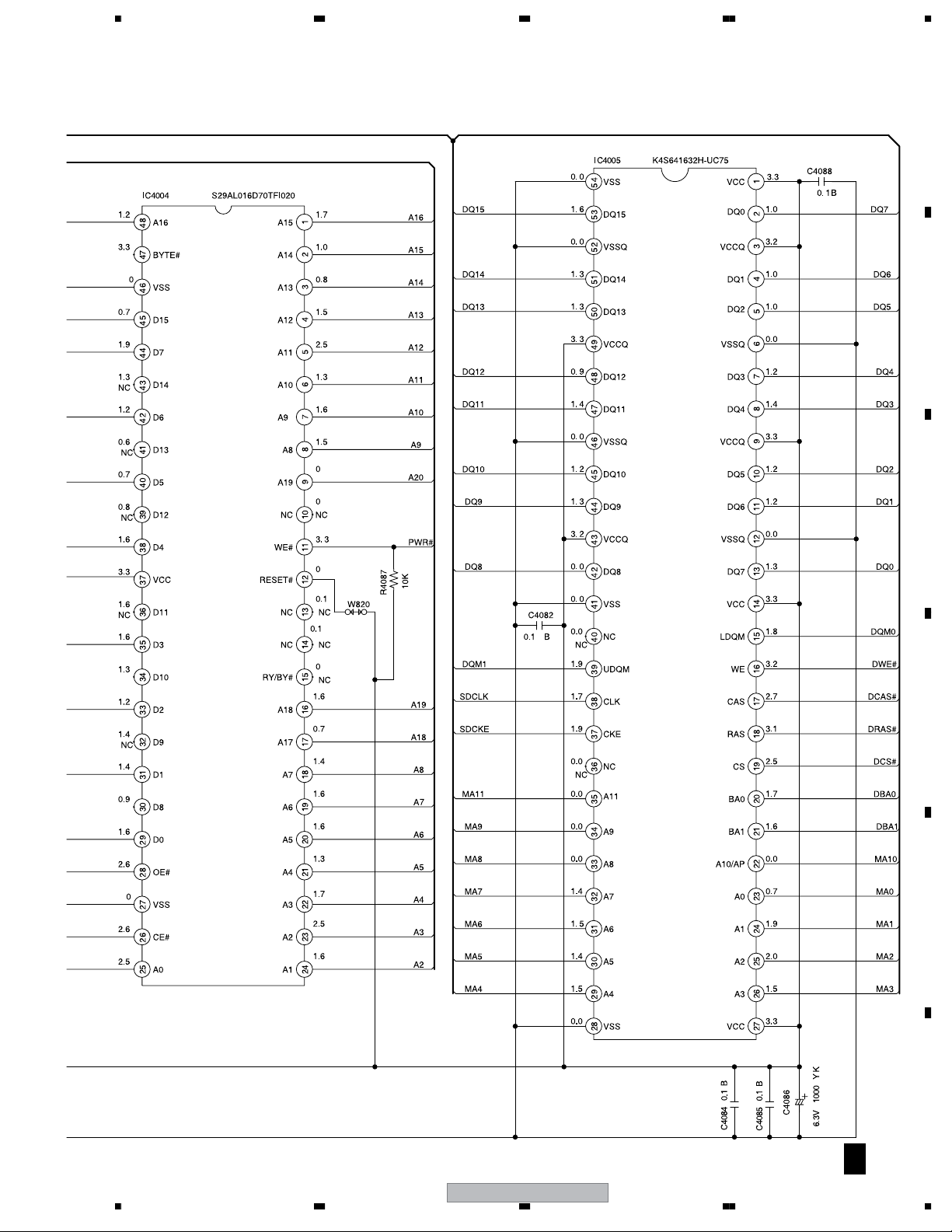
DVD MT PCB ASSY
A
SEMICONDUCTORS
IC4002 (MT1389EE/B2-L) MT1389EE/B2-L-K
IC4001 (BR24L16FJ-WE2) I57F04L160
IC2301 (LA6565-TE) I03F065650
IC4003 (BD5229G-TR) I97F052290
D
IC4004 (S29AL016D70TF1020) S2G602AF01
IC4005 (K4S641632H-UC75) IFLJ0632H7
>
IC4006 (SIP1117L-ADJ-TP) I1HF9117L0
IC7301 (MM1623BFBE) MM1623BF-TBB
IC8003-IC8005 (PMC1742KEG/2K) PCM1742KE-TBB
IC8006-IC8008 (BA4560F-E2) I07F045600
IC8001 (TC7SHU04FU) I55F004FU0
Q2301,Q8005,Q8011,Q8012(KTC3875S) TCAA3875SY
Q8008(KTC3875S) TCAA3875SY
Q2302-Q2305,Q8010 (KTA1504S) TAAA1504SY
Q8013,Q8014 (KTA1504S) TAAA1504SY
E
Q2306,Q2307 (2SK3018T106) T27T030180
Q8002-Q8004,Q8006 (DTC114YUA) TN7J407001
Q8007,Q8009 (DTC114YUA) TN7J407001
Q8015- Q8018 (2SD2114K) T97A021140
Q8020- Q8023 (2SD2114K) T97A021140
D8003 (UDZS6.8B) DE7RB6R82B
D8004-D8006 (1SS355) DD7R0S3550
B4001, B4002, B4008 (CHIP BEADS ) 0246C51024
(CHIP BEADS : MMZ1608R102CT)
B8001, B7304- B7305 (CHIP BEADS ) 0246C51024
F
(CHIP BEADS : MMZ1608R102CT)
X4001 CRYSTAL (27MHz) 100BT02701
OPERATION PCB ASSY
B
SEMICONDUCTORS
IC651 IC PT6315 PT6315
D651 1SS133T-77 D1VT001330
D652 1SS133T-77 D1VT001330
D654 1SS133T-77 D1VT001330
D655-D659 1SS133T-77 D1VT001330
D663 1SS133T-77 D1VT001330
D667 1SS133T-77 D1VT001330
SWITCHES AND RELAYS
SW663 SWITCH TACT 0504R01T38
SW666 SWITCH TACT 0504R01T38
OTHERS
V651 TUBE FLUORESCENT VAW1077
CP601 CONNECTOR PCB SIDE 069EVB3050
CP603 CONNECTOR PCB SIDE 069EV93050
DOUBLE, FACE-TAPE 7290000156
C
FL HOLDER 752WSA0466
OPERATION 2 PCB ASSY
SWITCHES AND RELAYS
SW660 SWITCH TACT 0504R01T38
SW662 SWITCH TACT 0504R01T38
SW664 SWITCH TACT 0504R01T38
SW665 SWITCH TACT 0504R01T38
SW663 SWITCH TACT 0504R01T38
OTHERS
CP605 CONNECTOR PCB SIDE 069EV53050
48
DV-686A-S
1234
Page 49

5678
Mark No. Description Part No.
POWER PCB ASSY
F
RESISTORS
R511 FUSE,Resistor R65584680J
OTHERS
CP502 CONNECTOR PCB SIDE 06C32E3504
J8102 RCA JACK 060Q401115
OS8101 OPTICAL DRIVICE 07AQ000009
CP8102 CONNECTOR PCB SIDE 06C3223003
OPERATION 3 PCB ASSY
G
SWITCHES AND RELAYS
SW667 SWITCH TACT 0504R01T38
OTHERS
OS651 REMOTE RECEIVER 077A040001
CP603 CONNECTOR PCB SIDE 069EV93050
CP604 CONNECTOR PCB SIDE 069EV53050
SW PCB ASSY
D
There is no Service Parts
A
>
B
C
LOADING MOTOR PCB ASSY
E
There is no Service Parts
D
E
56
DV-686A-S
F
49
7
8
Page 50

1234
6. ADJUSTMENT
6.1 WHEN REPLACING DVD DECK
A
WHEN REPLACING DVD DECK
[ Removing the DVD Deck ]
Before removing Pick Up PCB and DVD PCB connector, short circuit the position shown in Fig. 1 using
a soldering iron. If you remove the DVD Deck with no soldering, the Laser may be damaged.
[ Installing the DVD Deck ]
B
C
Remove all the soldering on the short circuit position after the connection of Pick Up PCB and DVD
PCB connector.
NOTE
•
Before your operation, please read “PREPARATION OF SERVICING” .
•
Use the Lead Free solder.
•
Manual soldering conditions
• Soldering temperature: 320 ± 20˚C
• Soldering time: Within 3 seconds
• Soldering combination: Sn-3.0Ag-0.5Cu
•
When Soldering/Removing of solder, use the draw in equipment over the Pick Up Unit to prevent the
Flux smoke from it.
Pick Up PCB
D
Fig. 1
E
F
Short circuit using a
soldering iron.
50
DV-686A-S
1234
Page 51

5678
6.2 TEST MODE
POWER ON
A
POWER
DVD test disc
(GGV1025)
ON
DISC SET
<TRAY OPEN> <TRAY CLOSE>
OPEN/CLOSE
(Player)
DVD disc
OPEN/CLOSE
(Player)
TEST MODE: PLAY
CHECK
<PLAY>
Press the play key
( ) of the normal
remote control unit.
ESC TEST
DVD, CD
Test mode remote control
unit (GGF1381)
An address is displayed
B
C
D
GGF1381
Test mode
remote control
unit
Notes:
• After going into test mode, if you play back the disc, "DISC-NON" is displayed.
• The video signal and the audio signal are outputted during the test mode.
• The SKIP key and the SCAN key are effective during the test mode.
DSC - &&&
TEST MODE: OFF
POWER
OR
GGF1381
Test mode
OFF
56
remote control
unit
DV-686A-S
ESC
7
E
F
51
8
Page 52

1234
6.3 TEST MODE IN
Test Mode Functional Specification
A
1 Test mode entry
In the power ON state, press the [ESC] (A8-5F) key and [TEST / RANDOM] (A8-5E) key in order of the Test mode remote control
unit.
• Light the all FL and LEDs.
• OSD displays test mode.
Note:
* When pressing the keys of something, the FL displays "NO DISC" and the LED lighting disappears.
2 Release the Test mode
• Turn off the power.
B
• Press the [ESC] (A8-5F) key of the remote control unit.
3 LD ON
DVD : Press the [TEST] (A8-5E) and [1] (A8-01) keys in order, and turn on the laser diode (650n).
CD : Press the [TEST] (A8-5E) and [4] (A8-04) keys in order, and turn on the laser diode (780n).
C
D
E
F
52
1234
DV-686A-S
Page 53

5678
6.4 DISC REMOVAL METHOD
DISC REMOVAL METHOD AT NO POWER SUPPLY
1.2.Slide the Rack Loading (White) toward the arrow direction by using a minus driver to release the lock.
(Refer to Fig. 1)
Manually open the Tray.
Rack Loading (White)
A
DVD Player (Bottom Side)
B
Fig. 1
PARENTAL CONTROL - RATING LEVEL
4 DIGIT PASSWORD CANCELLATION
If the stored 4 digit password in the Rating Level menu needs to be cancelled, please follow the steps
below.
Set the DVD to the Stand-by Mode.
1.
Press and hold the 'STOP' key on the front panel.
2.
Simultaneously press and hold the POWER key on the front panel.
3.
The 4 digit password has now been cleared.
4.
NOTE: The above procedure will reset ALL of the player's settings to the default factory state.
PREPARATION OF SERVICING
The laser diode used for a pickup head may be destroyed with external static electricity.
Moreover, even if it is operating normally after repair, when static electricity discharge is
received at the time of repair, the life of the product may be shortened.
Please perform the following measure against static electricity, be careful of destruction of a
laser diode at the time of repair.
C
D
E
• Place the unit on a workstation equipped to protect against static electricity, such as
conductive mat.
• Soldering iron with ground wire or ceramic type is used.
• A worker needs to use a ground conductive wrist strap for body.
56
DV-686A-S
7
F
53
8
Page 54

1234
7. GENERAL INFORMATION
7.1 DIAGNOSIS
7.1.1 DISPLAY SPECIFICATION OF THE TEST MODE
A
Character in bold : Item name
: Information display
1
5
6
12
B
10
11
1 Address indication
The address being traced is displayed in number.
(as for the DVD, indication of decimal number is possible.)
C
DVD : ID indication (hexadecimal number, 8 digits)
[∗ ∗ ∗ ∗ ∗ ∗ ∗ ∗]
CD : ID indication [∗ ∗ ∗ ∗ ∗ ∗ ∗ ∗]
2 Code indication of remote control unit [R – ∗ ∗ ∗ ∗]
In case of double code, display a 2nd code.
3 Main unit keycode indication [K – ∗ ∗]
2
3
7
8
9
13
14
15
0 Disc sensing [DSC – ∗ ∗ ∗]
The type of discs loaded is displayed.
[DVD], [CD ], [VCD], [ ]
- Jitter value [J – ∗ ∗ ∗ ∗] Note:Don’t use it.
= Version of the FL controller [FL: ∗ ∗ ∗ ∗]
~ Region setting of the player [REG: ∗]
Setting value : [1] to [6]
5 Tracking status [TRKG – ∗ ∗ ∗]
Tracking on : [ON]
Tracking off : [OFF]
D
6 Spindle status [SPDL – ∗ ∗ ∗]
[OFF], [CLV]
7 Mechanism (loading) position value [M – ∗ ∗]
Unknown : [01] or [41]
Open state : [04]
Close state : [08]
During opening : [12]
During closing : [22]
8 Slider position [S – ∗ ∗ ∗ ∗]
E
In Side Switch ON : [01]
In Side Switch OFF : [00]
9 Output video system [V – ∗ ∗ ∗ ∗]
NTSC system : [NTSC]
PAL system : [PAL]
Automatic setting : [AUTO]
Scart terminal output [SK – ∗ ∗]
(Display only the WY model which can do the output setting
of scart terminal.)
VIDEO : [00]
F
S-VIDEO : [01]
RGB : [02]
! Destination setting of the FL controller
[MDL: ∗ ∗ ∗ ∗ / ∗ ∗ ∗]
Four characters in the front represent code 01.
Three characters in the back represent the destination code.
J: /J, K: /KU, /KC, /KU/KC, R: /RL/RD, RAM : /RAM,
LB: /LB, WY: /WY
@ Version of the flash ROM [VERSION: ∗∗∗∗∗∗∗∗]
54
DV-686A-S
1234
Page 55

5678
7.1.2 FUNCTIONAL SPECIFICATION OF THE SHORTCUT KEY
Only during normal playback, the following shortcut keys can be assigned by pressing a required key after pressing the ESC
key of the remote control unit. To quit, press the ESC key
Only during normal playback, the following shortcut keys can be assigned by pressing a required key after pressing the ESC
key of the remote control unit. To quit, press the ESC key
Command Contents Conditions
Memory clear and region / revision indication CLEAR (∗1) A8-45
Memory clear and region / revision indication CLEAR (∗1) A8-45
Average value measurement of DVD error rate 5 (∗1) A8-05
Average value measurement of DVD error rate 5 (∗1) A8-05
CD error rate measurement 5 (∗1) A8-05
CD error rate measurement 5 (∗1) A8-05
Scart terminal output : VIDEO
Scart terminal output : VIDEO
Scart terminal output : S-VIDEO SUBTITLE AF-36
Scart terminal output : S-VIDEO SUBTITLE AF-36
Scart terminal output : RGB ANGLE AF-B5
Scart terminal output : RGB ANGLE AF-B5
Progressive OFF
Progressive OFF
Progressive ON F_SKIP A3-9C
Progressive ON F_SKIP A3-9C
ZOOM ON (X2 -> X4 -> x1) ZOOM AF-37
ZOOM ON (X2 -> X4 -> x1) ZOOM AF-37
Service mode indication (error rate indication, etc.) CHP/TIM (∗1) A8-13
Service mode indication (error rate indication, etc.) CHP/TIM (∗1) A8-13
Model information indication CHAP (∗1) A8-40
Model information indication CHAP (∗1) A8-40
Title search Input mode IN
Title search Input mode IN
Region confimation mode
Region confimation mode
Command Contents Conditions
WY, models equipped with Scart terminal
WY, models equipped with Scart terminal
Only for progressive models
Only for progressive models
Title No. input
Search execution
Title No. input
Search execution
Remote Control
Key Name
Remote Control
Key Name
AUDIO AF-BE
AUDIO AF-BE
R_SKIP A3-9D
R_SKIP A3-9D
SIDE A (∗1)
Numbers (∗1)
SIDE A (∗1)
PLAY (∗1)
Numbers (∗1)
PLAY (∗1)
A.MON (∗1)
Numbers (∗1)
A.MON (∗1)
Numbers (∗1)
∗1 : Test mode remote control unit
∗1 : Test mode remote control unit
Remote
Control Code
Remote
Control Code
A8-4D
A8-00 to A8-09
A8-00 to A8-09
A8-1E
A8-01 to A8-08
A8-01 to A8-08
A8-4D
A8-17
A8-17
A8-1E
A
B
• Service mode indication (ESC + CHP/TIM keys)
ID Address
• Service mode indication (ESC + CHP/TIM keys)
The error rate is always displayed in exponential notation, e.g., ∗.∗ ∗ e - ∗, for both DVDs and CDs.
ID Address
EDC/ID/AV 1 error history (ID Address, EDC/ID Error, last eight errors)
The error rate is always displayed in exponential notation, e.g., ∗.∗ ∗ e - ∗, for both DVDs and CDs.
EDC/ID/AV 1 error history (ID Address, EDC/ID Error, last eight errors)
• Calculation of the average error rate (ESC + "5" [Test mode remote control unit] keys)
The average of the last eight error rates is calculated and indicated in exponential notation. After the calculation is completed, "OK" or "NG" is
• Calculation of the average error rate (ESC + "5" [Test mode remote control unit] keys)
displayed. If "NG" is displayed, the disc tray will open (for both DVDs and CDs)
The average of the last eight error rates is calculated and indicated in exponential notation. After the calculation is completed, "OK" or "NG" is
For DVDs: OK with 5.0e-4 or less, for CDs: OK with 7.6e-3 or less
displayed. If "NG" is displayed, the disc tray will open (for both DVDs and CDs)
For DVDs: OK with 5.0e-4 or less, for CDs: OK with 7.6e-3 or less
• Indication of model information (ESC + CHAP keys)
The items from 12 to 15 of the TEST MODE Indications are displayed. However, in the indications, S in the standard test mode is changed to
• Indication of model information (ESC + CHAP keys)
CHIP VERSION, and M is changed to RF VERSION. For details, see 7.1.4.
The items from 12 to 15 of the TEST MODE Indications are displayed. However, in the indications, S in the standard test mode is changed to
CHIP VERSION, and M is changed to RF VERSION. For details, see 7.1.4.
• Region confirmation mode (ESC + A.MON [Test mode remote control unit] + "1"-"8" [Test mode remote control unit] keys)
After you press the A.MON key while holding the ESC key pressed and then input the region number, if the number is different from that set in
• Region confirmation mode (ESC + A.MON [Test mode remote control unit] + "1"-"8" [Test mode remote control unit] keys)
the unit, an error message is displayed, and the tray opens.
After you press the A.MON key while holding the ESC key pressed and then input the region number, if the number is different from that set in
the unit, an error message is displayed, and the tray opens.
C
D
E
56
DV-686A-S
F
55
7
8
Page 56

1234
7.1.3 SPECIFICATION OF MODEL INFORMATION DISPLAY
To display model information : Press the ESC key then the CHAP key.
To close the model information display : Press the ESC key.
A
• Display contents
AREA : WY REGION : 2
3
B
Don't care.
ROM NUMBER YAD5215B
REG CHK 40
1
2
5
Don't Care
6
C
SUM CHK D2AD
FL VERSION 1.08
CHIP VERSION 1389FE
1 Destination indication
Display it according to model information set from the FL Driver IC.
2 Region No.
3 ROM number
Rom display Version.
5 SUM CHK SUM value of E2P ROM displays with four places.
D
6 CHIP VERSION
Character in bold : Item name
: Information display
E
F
56
1234
DV-686A-S
Page 57

5678
7.1.4 FUNCTIONAL SPECIFICATION OF THE SERVICE MODE
• Display during Service Mode
To enter Service Mode, press the CHP/TIM key while holding the ESC key pressed.
To quit, press the ESC key.
Service mode display
1 ID Address
2 Error rate (always displayed), in exponential notation
ERROR RATE : ∗ ∗ ∗ ∗ ∗ ∗ ∗
( ∗ ∗ ∗ ∗ )
Number of error
• Calculation of the average error rate
For DVDs: OK with 5.0e-4 or less, for CDs: OK with 7.6e-3 or less
ex) For DVDs
• Step 1
%%e -&
• Step 2
%%e -4
A
B
%%e -6 : OK
%%e -5 : OK
%%e -4 : Refer to Step 2
%%e -3 : NG
%%e -2 : NG
3.0e -4 : OK
4.0e -4 : OK
5.0e -4 : OK
6.0e -4 : NG
7.0e -4 : NG
3 EDC/ID error history (ID Address, EDC/ID errors, last eight errors)
Note:
∗ Error of AV1 is not supported in this player.
Indication plan contents
1
2
C
3
D
Character in bold : Item name
: Information display
DV-686A-S
56
E
F
57
7
8
Page 58

1234
C
2
U
7.1.5 METHOD FOR DIAGNOSING DEGRADATION OF THE LDS ON THE PICKUP ASSY
Case when this diagnosis is required :
When playback of any disc, including a test disc (DVD: GGV1025, CD: STD-905), cannot be performed
A
How to diagnose
In the case mentioned above, degradation of the laser diodes (LDs) mounted on the PICKUP Assy is suspected.
Measure the voltage between the two ends of one of the resistors mentioned below.
No playback of a DVD :
Measure the voltage between the two ends of R2321 or R2323 on the DVDM
Assy. If the voltage is 0.4 V or higher, the 650-nm LD is degraded.
B
No playback of a CD :
Measure the voltage between the two ends of R2320 or R2322 on the DVDM
Assy. If the voltage is 0.4 V or higher, the 780-nm LD is degraded.
If the measurements show degradation
of an LD, replace the DVD MECHA
Assy.
C
To OPTICAL PICK
DVD MT PCB ASSY
CP2301
CP2301
C2301
D
C2311
R2335
R2338
CP2303
R2334
C2308
C2310
R2333
R2332
C2305
R2310
R2312
R2311R2313
R2337
R2316R2317
W809
W817
CP2303
R2318
Q2302
R2320
C4003
R2325
Q2304
C4002
R2326
R2327
E
W819
Q2303
R2322
C2320
R2321
R2323
Q2305
Q2307Q2306
R2306
303
R2307
R2308
Q2301
R2309
A
Front side
SIDE A
F
58
DV-686A-S
1234
Page 59

5678
7.1.6 TROUBLE SHOOTING
No. Symptoms Diagnosis Contents Possible Defective Points
1 The power is not turned on.
2 An opening screen is not
displayed on the monitor
(The FL display lights. The
mechanism does not work.)
Check the voltage of AT+3.3V, –28V and FLDC on the POWER
SUPPLY Unit.
Are wires of output connector (POWER PCB ASSY) and CP4003
(DVDM Assy) disconnected or damaged ?
Check that the voltage at IC651-pin 10 (K 1) on the FLKY Assy
becomes about 2.7V when the POWER key is pressed and 0 V when it
is released.
Check that the voltage at OS651-pin 1 (IR) on the OPERATION1 Assy
is in the range between 0 and 3.3 V while receiving signals from the
remote control unit when any key on it is pressed.
• Check the voltage of E+6.8V and SW+3.3V on the POWER SUPPLY
Unit.
• Check the voltage of P.ON-H is about 2.8V on the POWER SUPPLY
Unit.
POWER PCB ASSY
Connector / cable
OPERATION 2 Assy
Tact SW
(when operation of only the
POWER key on the main unit is
not accepted)
FLKY Assy
Remote receiver section
(when operation of only the
POWER key on the remote
control unit is not accepted)
POWER SUPPLY Unit
A
B
3
An opening screen is not
displayed on the monitor
(The FL display lights. The
mechanism does not work.)
Check that the following voltage are output :
IC4006-pin 5 : 1.8V, on the DVD MT PCB Assy.
Is a resonator (X4001 : 27MHz) on the DVDM Assy oscillating ?
• Is a signal input into IC4004-pin26 (PCE#) on the DVDM Assy ?
(Is a signal "H" for 80 mS and then "L" after the power is turned
on ?)
→ Communication with flash ROM.
• Are the signals input into IC4005-pin 16 (DWE#), pin 19 (DCS#)
and pin 38 (SDCLK) on the DVDM Assy ?
(Is a signal fluctuating ?)
→ Communication with SDRAM
Is a signal output from IC4004-pin 28 (PRD#) on the DVD MT Assy?
(Is a signal fluctuating for several hundred mS after the power is turned
on ?)
Are the signals of IC4001-pin 5(SDA) and pin 6(SCL) on the DVDM
Assy fluctuating for one or two seconds after the power is turned ?
Check the video signal path between DVD IC (DVD MT Assy IC4002)
and video-out terminal (see the block diagram)
DVD MT PCB Assy
1.8V Regulator IC (IC4006)
DVD MT PCB Assy
Crystal resonator (X4001)
DVD MT PCB Assy
DVD IC (IC4002)
Flash ROM (IC4004)
SDRAM (IC4005)
DVD MT PCB Assy
Flash ROM (IC4004)
DVD MT PCB Assy
EEPROM (IC4001)
DVD MT PCB Assy
Video circuit after DVD IC
(IC4002)
C
D
E
56
DV-686A-S
F
59
7
8
Page 60

1234
No. Symptoms Diagnosis Contents Possible Defective Points
4A tray cannot be opened.
(An opening screen is
A
B
C
D
displayed on the monitor)
5 Playback impossible
(no focusing)
6 Playback impossible
(Spindle does not turn)
7 Playback impossible
(Playback stops)
8 Picture disturbance during
playback
(block noise, freeze, other)
9 No sound
(Picture is normal)
Does the voltage of CP2302-pin 3 and pin 1 on the DVD MT Assy
change normally ?
Pin 5 (SW2(TRIN)): Tray is fully closed: "L"
Pin 3 (SW1(TROUT)): Tray is fully opened: "L"
Is a LOAD-DRV signal reaching ?
Are the signals output from IC2301-pin 36 and pin 37 (CP2302-pin 4
and pin 5) on the DVDM Assy ?
Pin 4: Approx. 4.5V during opening tray approx. 0V during closing tray.
Pin 5: Approx. 0V during opening tray approx. 4.5V during closing tray.
Are wires of CP2302 and CP2303 on the DVDM Assy disconnected or
damaged ?
Does the voltage of CD2301-pin 5 change by pressing the Inside
switch.
Are the signals output from IC2301-pin 9 (F+) and pin 8 (F–) on the
DVDM Assy ?
Does 650-nm LD emit light ?
Does a pickup lens move up / down ?
Does an actuator spring bend ?
Are plastic parts damaged ? Or is a shaft detached ?
Is the turntable detached or tilted ?
Is flexible cable of CP2301 on the DVD MT Assy disconnected or
damaged ?
Is signal output from IC4002-pin 42 (FOSO) on the DVDM Assy ?
(Device control of about 1.4 V is output usually. It is fluctuated by about
± 250 mV with focus up / down.)
Are the signals output from IC2301-pin 10 (MOT SPDL–), and pin 11
(MOT SPDL+) on the DVD MT Assy ?
Is pin 33,34 (STBY) fixed LOW?
Is there any part detached from the spindle motor ?
Or Is there any foreign object lodged in it ?
Are wires of CP2303 on the DVD MT Assy disconnected or damaged ? Flexible cable / connector
Is signal output from IC4002-pin 37 (DMSO) on the DVDM Assy ?
Does 650-nm LD deteriorate ?
If the voltage at each both ends of R2303 and R2305 on the DVD MT
Assy is 0.4 V or more, the 650-nm LD is definitely deteriorated.
Does 780-nm LD deteriorate ?
If the voltage at each both ends of R2302 and R2304 on the DVD MT
Assy is 0.4 V or more, the 780-nm LD is definitely deteriorated.
Are there scratches or dirt on the disc ? Disc
Are there scratches or dirt on the disc ?
Is there a problem with the format of the disc ?
Check the waveform (ABCK, ALRCK, ACLK, ASDATA).
Is signal output from IC8004-pin 7 and pin 8 on the DVD MT Assy ? DVD MT PCB Assy
Tray SW
DVD MT PCB Assy
DVD IC (IC4002)
DVD MT PCB Assy
FTS Driver IC (IC2301)
Connector / cable
Inside switch
DVD MT PCB Assy
FTS Driver IC (IC2301)
Pickup
Mechanism section (motor)
Flexible cable / connector
DVD MT PCB Assy
DVD IC (IC4002)
DVD MT PCB Assy
FTS Driver IC (IC2301)
Mechanism section
(Spindle motor)
DVD MT PCB Assy
DVD IC (IC4002)
650-nm LD deteriorated.
(When playback of a DVD is
impossible)
780-nm LD deteriorated.
(When playback of a CD is
impossible)
Disc
DVD MT PCB Assy
DVD IC (IC4002)
Audio Dac IC (IC8004)
Symptoms That May Occur When Any Of The Following ICs Is In Failure
E
IC Symptoms
EEP ROM
(DVD MT Assy : IC4001)
16M Flash ROM
(DVD MT Assy : IC4004)
DVD IC
(DVD MT Assy : IC4002)
64M SDRAM
(DVD MT Assy : IC4005)
F
60
1234
User's data cannot be stored in memory.
The ID number is lost.
The power cannot be turned on.
Downloading of the firmware cannot be performed.
Any kind of symptoms (no power, a failure in any of the servo, video and audio systems, etc.) may be
generated, because the DVD processing is performed by a single chip.
No power.
Block noise is generated during playback.
DV-686A-S
Page 61

5678
7.2 DISASSEMBLY
REMOVAL OF MECHANICAL PARTS AND P.C. BOARDS
1-3: DVD DECK (Refer to Fig. 1-3)
1.
Short circuit the position shown in Fig. 1-3 using a
TOP CABINET/FRONT CABINET/OPERATION
1-1:
1/2PCB (Refer to Fig. 1-1)
1.
Remove the 5 screws 1.
2.
Remove the Top Cabinet in the direction of arrow (A).
3.
Disconnect the following connector: (CP4002).
4.
Unlock the 4 supports 2.
5.
Remove the Front Cabinet in the direction of arrow (B).
6.
Remove the 11 screws 3.
7.
Remove the Operation 1/2 PCB in the direction of arrow
.
(C).
Top Cabinet
1
Operation 3 PCB
1
1
soldering iron. If you remove the DVD Deck with no
soldering, the Laser may be damaged.
2.
Disconnect the following connectors:
(CP2301, CP2302, CP2303).
3.
Remove the 4 screws 1.
4.
Remove the DVD Deck in the direction of arrow.
DVD Deck
A
1
1
1
1
Short circuit using a
soldering iron.
B
Pick Up PCB
Operation 2 PCB
3
3
(C)
2
2
Front Cabinet
3
3
3
3
(B)
(C)
2
3
3
3
(C)
2
(A)
3
3
Operation PCB
1-2: POWER PCB (Refer to Fig. 1-2)
Disconnect the following connectors:
1.
(CP4003, CP8001).
2.
Remove the 3 screws 1.
Remove the 4 screws 2.
3.
Remove the Power PCB in the direction of arrow.
4.
2
2
2
2.
2
Power PCB
1
1
1
1
Fig. 1-1
1
Fig. 1-3
C
NOTE
1.
Before your operation, please read “PREPARATION
OF SERVICING”.
2.
Use the Lead Free solder.
3.
Manual soldering conditions
• Soldering temperature: 320 ± 20˚C
• Soldering time: Within 3 seconds
• Soldering combination: Sn-3.0Ag-0.5Cu
4.
When Soldering/Removing of solder, use the drawing
equipment over the Pick Up Unit to prevent the Flux
smoke from it.
5.
When installing the DVD Deck, remove all the soldering
D
on the short circuit position after the connection of Pick
Up PCB and DVD PCB connector.
1-4: DVD PCB (Refer to Fig. 1-4)
Remove the 4 screws 1.
1.
Remove the 4 screws 2.
2.
Remove the DVD PCB in the direction of arrow.
3.
2
2
2
2
E
Fig. 1-2
DV-686A-S
56
DVD PCB
1
1
1
1
Fig. 1-4
F
61
7
8
Page 62

1234
7.3 DVD DECK SECTION
A
B
REMOVAL OF DVD DECK PARTS
NOTE
1. Do not disassemble the DVD DECK PARTS except
listed parts here. Minute adjustments are needed if the
disassemble is done. If the repair is needed except
listed parts, replace the DVD MECHA ASS'Y.
2-1: TRAY (Refer to Fig. 2-1-A)
Set the Tray opened. (Refer to the DISC REMOVAL
1.
METHOD AT NO POWER SUPPLY)
Unlock the 3 supports 1 and draw it while sagging the
2.
Tray.
Loader Ass'y
NOTE
In case of the Traverse Ass'y, install it from (1) to (4) in
1.
order. (Refer to Fig. 2-2-B)
In case of the Traverse Ass'y installation, hook the wire
2.
on the Loader Ass'y as shown Fig. 2-2-C.
Loader Ass'y (Bottom Side)
Rack Loading
Holder Traverse
1
Tray
C
NOTE
In case of the Tray installation, install them as the circled
1.
section of Fig. 2-1-B so that the each markers are met.
Loader Ass'y
D
Tray
2-2: TRAVERSE ASS'Y (Refer to Fig. 2-2-A)
Remove the screw 1.
1.
Unlock the 2 supports 2.
2.
3.
Remove the Insulator (R) from the Loader Sub Ass'y.
4.
Remove the Traverse Ass'y.
E
2
1
1
Traverse Ass'y
Fig. 2-1-A
Check Lock
Check Hook
Fig. 2-2-B
Loader Ass'y
Fig. 2-2-C
2-3: LOADING MOTOR PCB ASS'Y/ LOADING BELT
(Refer to Fig. 2-3-A)
1.
Remove the Loading Belt.
Fig. 2-1-B
1
2.
Remove the screw 1.
3.
Remove the Loading Motor PCB Ass'y.
4.
Remove the 2 screws 2.
5.
Remove the Loading Motor.
6.
Remove the Gear Pulley.
Loading Belt
2
2
2
Loader Sub Ass'y
Gear Pulley
Insulator (R)
Traverse Ass'y
F
• Screw Torque: 2.0 ± 0.3kgf•cm
62
1234
Fig. 2-2-A
DV-686A-S
• Screw Torque: 2.5 ± 0.3kgf•cm (Screw 1)
• Screw Torque: 1.0 ± 0.3kgf•cm (Screw 2)
Loading Motor
Loading Motor PCB Ass’y
1
Fig. 2-3-A
Page 63

5678
NOTE
1.
In case of the Pulley Motor installation, check if the value
of the Fig. 2-3-B is correct.
2.
When installing the wire of the Loading Motor PCB Ass'y,
install it correctly as Fig. 2-3-C.
Manual soldering conditions
• Soldering temperature: 320 ± 20 ˚C
• Soldering time: Within 3 seconds
• Soldering combination: Sn-3.0Ag-0.5Cu
When installing the Loading Motor PCB Ass'y, install it
3.
correctly as Fig. 2-3-D.
In case of the Loading Motor PCB Ass'y installation, hook
4.
the wire on the Loader Sub Ass'y as shown Fig. 2-3-E.
Pulley Motor
Loading Motor
Safety surface for pressing
of the insert.
BROWN (1)
WHITE (2)
7.0 ± 0.1mm
Fig. 2-3-B
2-4: RACK LOADING/MAIN GEAR/PULLEY GEAR
(Refer to Fig. 2-4-A)
1.
Unlock the support 1 and remove the Gear Pulley.
2.
Remove the Gear Main.
3.
Press down the catcher 2 and slide the Rack Loading.
Gear Pulley
Gear Main
2
1
Rack Loading
Loader Sub Ass’y
Fig. 2-4-A
NOTE
1.2.In case of the Rack Loading installation, hook the Rack
Loading on the Loader Sub Ass'y as shown Fig. 2-4-B.
When installing the Gear Main, take care the direction
of up or down as shown Fig. 2-4-C.
Rack Loading
A
B
C
Rack Loading
Check Hook
Check Hook
Loading Motor PCB Ass’y
AB
The Lever should be position
between A and B.
Check Hook
Loading Motor PCB Ass’y
Fig. 2-3-C
Fig. 2-3-D
Fig. 2-3-E
Loader Sub Ass'y (Bottom Side)
Check Hook
Fig. 2-4-B
Up Side
Main Gear
Down Side
Fig. 2-4-C
2-5: CLAMPER ASS'Y (Refer to Fig. 2-5-A)
Press the Clamper and rotate the Plate Clamper clockwise,
1.
then unlock the 3 supports 1.
Remove the Plate Clamper, Magnet Clamper and Clamper.
2.
Plate Clamper
Magnet Clamper
Main Frame
1
1
Clamper
1
Fig. 2-5-A
D
E
56
DV-686A-S
F
63
7
8
Page 64

1234
NOTE
1. In case of the Clamper Ass'y installation, install
A
correctly as Fig. 2-5-B.
Feed Motor
Gear Motor
Plate Clamper
Clamper
2-6:
B
HOLDER TRAVERSE/INSULATOR (F)/INSULATOR
(R) (Refer to Fig. 2-6-A)
Remove the Holder Traverse.
1.
Remove the 2 Insulator (F).
2.
Remove the Insulator (R).
3.
Traverse Ass'y
Insulator (F)
Holder Traverse
Check Lock
C
Insulator (F)
NOTE
1. In case of the Insulator (F) installation, install correctly
as Fig. 2-6-B.
Insulator (F)
D
Traverse Holder
Fig. 2-5-B
Insulator (R)
Fig. 2-6-A
5
Traverse Ass'y
Rack Feed Ass'y
• Screw Torque: 1.3 ± 0.3kgf•cm (Screw 2)
• Screw Torque: 3.0 ± 0.3kgf•cm (Screw 34)
• Screw Torque: 1.0 ± 0.3kgf•cm (Screw , 5 )
1
5
Gear Feed
4
Gear Middle
2
Switch PCB Ass'y
3
Fig. 2-7-A
NOTE
1.
When installing the Rack Feed Ass'y, push both ends to
align the teeth as shown Fig. 2-7-B. Then install it.
In case of the Gear Motor installation, check if the value
2.
of the Fig. 2-7-C is correct.
When installing the wire of the Switch PCB Ass'y, install
3.
it correctly as Fig. 2-7-D.
Manual soldering conditions
• Soldering temperature: 320 ± 20 ˚C
• Soldering time: Within 3 seconds
• Soldering combination: Sn-3.0Ag-0.5Cu
After the assembly of the Traverse Ass'y, hook the wire
4.
on the Traverse Ass'y as shown Fig. 2-7-E.
Rack Feed Ass'y
Push
Push
Fig. 2-6-B
SWITCH PCB ASS'Y/GEAR MIDDLE/GEAR FEED/RACK
2-7:
[OK] [NG]
FEED ASS'Y/FEED MOTOR (Refer to Fig. 2-7-A)
Unlock the support 1.
1.
Remove the Gear Middle.
2.
Remove the screw 2.
3.
4.
E
F
Remove the Rack Feed Ass'y.
5.
Remove the screw 3.
6.
Remove the Switch PCB Ass'y.
7.
Remove the screw 4.
8.
Remove the Gear Feed.
9.
Remove the 2 screws 5.
10.
Remove the Feed Motor.
11.
Remove the Gear Motor.
64
1234
DV-686A-S
Gear Motor
Feed Motor
Safety surface for pressing
of the insert.
8.0 ± 0.2mm
Fig. 2-7-B
Fig. 2-7-C
Page 65

5678
Switch PCB Ass'y
~ SPINDLE MOTOR ~
Check Hook
• Loosen the wirein the direction of the arrows.
Traverse Ass'y
Check Hook
Check Hook
YELLOW (2)
GREEN (1)
Check Hook
2-8: FFC WIRE HANDLING
~ FEED MOTOR ~
WHITE (4)
BROWN (3)
• Install wire from(1) to (4) in order.
Fig. 2-7-D
Fig. 2-7-E
A
B
C
1.
When installing the FFC, fold it correctly and install it as
shown from Fig. 2-8.
NOTE
Do not make the folding lines except the specified
1.
positions for the FFC.
[ 24 pin FFC ]
Printing _Serface
85±1 mm
Reinforcement Plat
To Pick Up PCB
Fig. 2-8
D
E
56
DV-686A-S
F
65
7
8
Page 66

1234
7.4 IC INFORMATION
• The information shown in the list is basic information and may not correspond exactly to that shown in the schematic diagrams.
A
List of IC
MT1389EE/B2-L, LA6565, PT6315
MT1389EE/B2-L (DVD MT ASSY: IC4002)
• MPEG / MICON / RF-AMP
Pin Arrangement (Top view)
252
255256
253254
110
B
C
D
E
AGND
DVDA
3
DVDB
4
DVDC
5
DVDD
6
DVDRF[P
7
NC
DVDRF[N
8
MA
9
MB
MC
MD
111213141516171819 22021222324
SA
NC
NC
SB
NC
SC
NC
SD
NC
CDFON
NC
CDFOP
TNI
TPI
MIDI1
MIDI2
LDO2
LDO1
SVDD3
CSO/RFOP
2526272829
RFLV/RFON
SGND
V2REFO
V20
VREFO
30313233343536373839
FEO
TEO
TEZIS[LV
TROPENPWM
PWMOUT1/V_ADIN9
40414243444546474849
NC
NC
USB_VDD3
FG/V_ADIN8 (PU)
TDI/V_ADIN4 (JTAG)
TMS/V_ADIN5 (JTAG)
TCK/V_ADIN6 (JTAG)
50
TDO/V_ADIN7 (JTAG)
51525354
IOA2 (PU)
IOA3 (PU)
IOA4 (PU)
55
IOA5 (PU)
56575859
IOA6 (PU)
IDA7 (PU)
IOA18 (PU)
6061626364
IOA19 (PU)
65 66
OP_OUT
OP_INN
OP_INP
DMO
FMO
TRO
FDO
USB_VSS
NC
NC
DVDD18
HIGHA0 (PU)
DVSS
APLLCAP
APLLVSS
67 68 69
NC
OSP
HIGHA5 (PU)
HIGHA6 (PU)
70
250251
NC
HRFZC
CRTPLP
RFGND
RFRPAC
OSN
253
RFGC
254
IREF
255
AVDD3
256
Data
PLL
APLL
65
APLLVSSVDD3
66
XIOWR
67
A16
68
HIGHA7 (PU)
DVDD3
HIGHA2 (PU)
HIGHA3 (PU)
HIGHA4 (PU)
71
HIGHA1 (PU)
72 73 74 75 76 77 78 79
NC
NC
RFVDD3
RFRPDC
108
Mhz
DLL
RF
Circuits
INT_ADDA
IOCA1 (PU)
IOA20
XIOCS (PU)
XIODE
241242243244245246247248249
ADCVSS
DVDD3
808182
NC
LPFIP
LPFIN
LPFON
LPFOP
ADCVDD3
PLLVDD3
IDACEXLP
PLLVSS
DMPLL DMPLL
AD0
AD1
AD2
AD3
DVSS (18)
AD4
AD5
AD6
83
84 85 86 87 88 89
IOA2/V_ADIN0
90 919293
XTALI
JITFO
JITFN
XTALO
SPDIF
DVDD18
(3) DVSS
RFGND18
RFVDD18
MC_DATA (PD)
(PD) ASDATA2
(PD) ASDATA3
(PD) ASDATA4
(PD) ASDATA1
(PD) ASDATA0
MPEG/MICON/RF-AMP
IC4002
MT1389EE/B2-L
ALE (PU)
AD7
A17
DVSS (3)
XUWR (PU)
XURD (PU)
DVDD18
UP1_2 (PU)
UP1_3 (PU)
UP1_4 (PU)
UP1_5 (PU)
UP1_6 (PU)
UP1_7 (PU)
IOA0 (PU)
94 95
96 97 98
100
99
UP3_0 (PU)
102
104
105
103
101
ABCK
ACLK
DVDD3
(18) DVSS
(PD) ALRCK
DVDD3
UP3_1 (PU)
UP3_4 (PU)
PU3_5 (PU)
ICE (PD)
106
107 108 109110 111 112 113
NC
SPMCLK
SPDATA
SPLRCK
SPBCK/ADTA5
HSYN/V_ADIN2
192
191
190
189
125
126
127
128
DQM0
DQS0
XPRST (PU)IRXINT0 (PU)
114
YUV5/B
YUV6/R
YUV4/G
DVDD3
DACVSSA
DACVDDA
DACVSSB
DVSS (3)
RD4
YUV3/CVBS
(PU) RD3/ASDATA5
RD3
DVDD18
RD2
RD1
(PD) DQM2
(PD) DQM3
(PU) RD30
(18) DVSS
(18) DVSS
VSYN/V_ADIN1
YUT7/ASDATA5
YUV0/CIN
FS
VREF
DACVDDC
VIDEO
DAC
RD0
RD15
DVDD3
RD14
RD5
RD7
DVSS (18)
RD6
115
116 117 118119 120 121 122 123124 125 126 127128
YUV2/C
DACVDDB
DVDD3
DVDD18
DVDD3
(3)DVSS
RCLK
DVDD3
DVDD18
(3) DVSS
DVDD3
XRAS
XCAS
XRWE
DQM1
DQS1
(3) DVSS
RD24
RD25
RD26
RD29
RA4
RA11
CKE
RA10
BA0
XRCS
RD8
RD9
RD10
RD11
RD12
RD13
193194195196197198199200201202203204205206207208209210211212213214215216217218219220221222223224225226227228229230231232233234235236237238239240
YUV1/Y
NC
NC
NC
NC
NC
NC
NC
NC
NC
NC
NC
RA5
RA6
RA7
RA8
RA9
NC
NC
RA3
RA2
RA1
RA0
BA1
DACVSSC
NC
NC
NC
NC
NC
NC
NC
NC
NC
NC
NC
NC
NC
129130 131 132 133134 135 136 137138 139 140 141142 143144 145 146 147 148149 150 151152 153 154155 156 157 158 159 160 161162 163 164 165166 167 168 169170 171 172173 174175 176 177 178179 180 181 182 183 184185 186 187 188189 190 191192
F
66
DV-686A-S
1234
Page 67

5678
• MPEG / MICON / RF-AMP Microcomputer
Block Diagram
DVD
PUH
Module
Motor
Drive
FLASH
ROM
DRAM
RF Amplifier
Servo IO
Spindle
Control
Memory
Controller
Debug
Port
Servo
Processor
Audio
DSP
108Mhz
TV Encoder
Video
Processor
Video Decoder
A
CVBS, Y/C
Component
Videop
Video DAC
B
De-
interlacer
MPEG-1/2
JPEG
C
GPIO
IR/VFD
System
CPU
System
Parser
CPPM/CPRM
DRM
32-bit
RISC
Audio
Output
PCM
Audio
DAC
SPDIF
D
E
56
DV-686A-S
F
67
7
8
Page 68

1234
MT1389EE/B2-L (DVD MT ASSY : IC4002)
• MPEG/MICON/RF-AMP CPU
Pin Function
A
No. Pin Name I/O Pin Function No. Pin Name I/O Pin Function
1 AGND – Analog ground
2 DVDA I AC coupled input path A
3 DVDB I AC coupled input path B
4 DVDC I AC coupled input path C
5 DVDD I AC coupled input path D
6 DVDRFIP I AC coupled DVD RF signal input RFIP
7 DVDRFIN I AC coupled DVD RF signal input RFIN
8MA I
9MB I
B
10 MC I DC coupled main-beam RF signal input C
11 MD I
12 SA I DC coupled sub-beam RF signal input A
13 SB I DC coupled sub-beam RF signal input B
14 SC I DC coupled sub-beam RF signal input C
15 SD I DC coupled sub-beam RF signal input D
16 CDFON I CD focusing error negative input
17 CDFOP I CD focusing error positive input
18 TNI I
19 TPI I 3 beam satellite PD signal positive input
C
20 MDI1 I Laser power monitor input
21 MDI2 I Laser power monitor input
22 LDO2 O Laser driver output
23 LDO1 O Laser driver output
24 SVDD3 – Analog power 3.3V
25 CSO O
26 RFLVL O
27 SGND – Analog ground
28 V2REFO – Reference voltage 2.8V
29 V20 I/O Reference voltage 2.0V
D
30 VREFO I/O Reference voltage 1.4V
31 FEO O Focus error monitor output
32 TEO O Tracking error monitor output
33 TEZISLV I/O TE Slicing Level
34 OP_OUT O Op amp output
35 OP_INN I Op amp negative input
36 OP_INP I Op amp positive input
37 DMO O Disk motor control output. PWM output
38 FMO O Feed motor control. PWM output
39
TROPENP/WM
E
40 PWMOUT1 O
41 TRO O Tracking servo output. PDM output of
42 FOO O Focus servo output. PDM output of
43 DVSS – 1.8V Ground pin for internal digital
44 NC – –
45 NC – –
46 DVDD3 –
47
FG(Diogital pin)
F
DC coupled main-beam RF signal input A
DC coupled main-beam RF signal input B
DC coupled main-beam RF signal input D
3 beam satellite PD signal negative input
Central servo/Positive main beam summing output
RFRP low pass, or Negative main beam summing output
O Tray PWM output/Tray open output
1st General PWM output, or Version AD input9
tracking servo compensator.
focus servo compensator
3.3V power pin for internal digital circuitry
–
Motor Hall sensor input, or Version AD input 8
48 TDI I
49 TMS I
50 TCK I
51 TDO I
52 DVDD18 –
53 IOA2 I/O Microcontroller address 2/IO
54 IOA3 I/O Microcontroller address 3/IO
55 IOA4 I/O Microcontroller address 4/IO
56 IOA5 I/O Microcontroller address 5/IO
57 IOA6 I/O Microcontroller address 6/IO
58 IOA7 I/O Microcontroller address 7/IO
59 HIGHA0 I/O Microcontroller address 8
60 IOA18 I/O Flash address 18/IO
61 IOA19 I/O Flash address 19/IO
62 DVSS –
63 APLLCAP I APLL External Capacitance connection
64 APLLVSS – Ground pin for sudio clock circuitry
65 APLLVDD3 – 3.3V Power pin for audio clock circuity
66 IOWR# I/O Flash write enable, active low/IO
67 A16 O Flash adress 16
68 HIGHA7 I/O Microcontroller address 15
69 HIGHA6 I/O Microcontroller address 14
70 HIGHA5 I/O Microcontroller address 13
71 HIGHA4 I/O Microcontroller address 12
72 HIGHA3 I/O Microcontroller address 11
73 DVDD3 –
74 HIGHA2 I/O Microcontroller adress 10
75 HIGHA1 I/O Microcontroller adress 9
76 IOA20 I/O Flash adress 20/IO
77 IOCS# I/O Flash chip select, active low/IO
78 IOA1 I/O Microcontroller adress 1/IO
79 IOOE# I/O Flash output enable, active low/IO
80 DVDD3 –
81 AD0 I Microcontroller address/data 0
82 AD1 I Microcontroller address/data 1
83
AD2
84
AD3
85
DVSS
86
AD4
87 AD5 I Microcontroller address/data 5
88 AD6 I Microcontroller address/data 6
89 IOA21 I/O
90 ALE I/O Microcontroller address latch enable
Serial interface port 3 data-out
Version AD input port 4
GPIO
Serial interface port 3 data-in
Version AD input port 5
GPIO
Serial interface port 3 clock pin
Version AD input port 6
GPIO
Serial interface port 3 chip-select
Version AD input port 7
GPO
1.8V power pin for internal digital circuitry
3.3V Ground pin for internal digital circuitry
3.3V power pin for internal digital circuitry
3.3V power pin for internal digital circuitry
I Microcontroller address/data 2
I Microcontroller address/data 3
1.8V Ground pin for internal digital circuitry
–
I Microcontroller address/data 4
Flash address 21/IO
While External FLASH size <= 2MB:
Version AD input port 0, or
GPIO
68
DV-686A-S
1234
Page 69

5678
No. Pin Name I/O Pin Function No. Pin Name I/O Pin Function
91 AD7 I Microcontroller address/data 7
92 A17 O Flash address 17
93 IOA0 I/O Microcontroller address 0/IO
94 DVSS –
3.3V Ground pin for internal digital circuitry
95 UWR# I Microcontroller write strobe, active low
96 URD# I Microcontroller read strobe, active low
97 DVDD18 –
1.8V power pin for internal digital circuitry
98 UP1_2 I/O Microcontroller port 1-2
99 UP1_3 I/O Microcontroller port 1-3
100 UP1_4 I/O Microcontroller port 1-4
101 UP1_5 I/O Microcontroller port 1-5
102 UP1_6 I/O
103 UP1_7 I/O Microcontroller port 1-7
Microcontroller port 1-6
2
C clock pin
I
2
C data pin
I
104 UP3_0 I/O Microcontroller port 3-0
8032 RS232 RXD
105 UP3_1 I/O Microcontroller port 3-1
8032 RS232 TXD
106 UP3_4 I/O
107 UP3_5 I/O
108 DVDD3 –
Microcontroller port 3-4
Hardwired RD232 RXD
2
I
C clock pin
Microcontroller port 3-5
Hardwired RD232 TXD
2
I
C data pin
3.3V power pin for internal digital circuitry
109 ICE I Microcontroller ICE mode enable
110 PRST# I Power on reset input, active low
111 IR I IR control signal input
112 INT0# I/O
Microcontroller external interrupt 0, active low
113 DQM0 I/O Data mask 0
114 DQS0 I/O GPIO
115 RD7 I/O
116 DVSS –
DRAM data 7
1.8V Ground pin for internal digital circuitry
117 RD6 I/O DRAM data 6
118 RD5 I/O DRAM data 5
119 DVSS –
3.3V Ground pin for internal digital circuitry
120 RD4 I/O DRAM data 4
121 RD3 I/O DRAM data 3
122 DVDD18 –
1.8V power pin for internal digital circuitry
123 RD2 I/O DRAM data 2
124 RD1 I/O DRAM data 1
125 RD0 I/O DRAM data 0
126 RD15 I/O
127 DVDD3 –
DRAM data 15
3.3V power pin for internal digital circuitry
128 RD14 I/O DRAM data 14
129 RD13 I/O DRAM data 13
130 RD12 I/O DRAM data 12
131 RD11 I/O DRAM data 11
132 RD10 I/O DRAM data 10
133 RD9 I/O DRAM data 9
134 DVSS –
3.3V Ground pin for internal digital circuitry
135 RD8 I/O DRAM data 8
136 DQS1 I/O GPIO
137 DQM1 I/O Data mask 1
138 RWE# O DRAM Write enable, active low
139 CAS# O
DRAM column address strobe, active low
140 RAS# O DRAM row address strobe, active low
141 DVDD3 –
3.3V power pin for internal digital circuitry
142 RCS# O DRAM chip select, active low
143 BA0 I/O DRAM bank address 0
144 DVSS –
1.8V Ground pin for internal digital circuitry
145 BA1 I/O DRAM bank address 1
146 RA10 I/O DRAM address 10
147 RA0 I/O DRAM address 0
148 DVSS –
3.3V Ground pin for internal digital circuitry
149 RA1 I/O DRAM address 1
150 RA2 I/O DRAM address 2
151 RA3 I/O DRAM address 3
152 DVDD18 –
1.8V power pin for internal digital circuitry
153 NC – –
154 NC – –
155 DVDD3 –
3.3V power pin for internal digital circuitry
156 RCLK I/O Dram clock
157 CKE O DRAM clock enable
158 RA11 I/O DRAM address bit 11
159 RA9 I/O DRAM address 9
160 RA8 I/O DRAM address 8
161 DVSS –
3.3V Ground pin for internal digital circuitry
162 RA7 I/O DRAM address 7
163 DVSS –
164 RA6 I/O
1.8V Ground pin for internal digital circuitry
DRAM address 6
165 RA5 I/O DRAM address 5
166 RA4 I/O DRAM address 4
167 DVDD3 –
168 RD31 I/O
3.3V power pin for internal digital circuitry
GPIO
169 RD30 I/O GPIO
170 RD29 I/O GPIO
171 NC –
–
172 NC – –
173 DVDD18 –
1.8V power pin for internal digital circuitry
174 RD26 I/O GPIO
175 NC –
–
176 RD25 I/O GPIO
177 RD24 I/O GPIO
178 DQM3 I/O GPIO
179 DQM2 I/O GPIO
180 NC – –
181 NC – –
182 DVDD3 –
3.3V power pin for internal digital circuitry
183 NC – –
184 NC – –
185 NC – –
186 NC – –
187 NC – –
188 NC – –
A
B
C
D
E
F
56
DV-686A-S
69
7
8
Page 70

1234
No. Pin Name I/O Pin Function No. Pin Name I/O Pin Function
189 DACVDDC – 3.3V power pin for VIDEO DAC circuitry
190 VREF – Bandgap reference voltage
A
191 FS – Full scale adjustment
192 YUV0 O Video data output bit 0
193 DACVSSC – Ground pin for VIDEO DAC circuitry
194 YUV1 O
195 DACVDDB – 3.3V power pin for VIDEO DAC circuitry
196 YUV2 O Video data output bit 2
197 DACVSSB –
B
198 YUV3 O Video data output bit 3
199 DACVDDA – 3.3V power pin for VIDEO DAC circuitry
200 YUV4 O Video data output bit 4
201 DACVSSA –
202 YUV5 O Video data output bit 5
203 YUV6 O Video data output bit 6
C
204 DVDD3 –
205 VSYN I/O Vertical sync input/output
206 YUV7 I/O Video data output bit 7
D
207 HSYN I/O Horizontal sync input/output
208 SPMCLK I/O
209 SPDATA I/O
E
210 SPLRCK I/O
211 SPBCK I/O Audio bit clock of SPDIF input
212 DVDD3 –
F
Compensation capacitor
Video data output bit 1
Analog Y output
Analog chroma output
Ground pin for VIDEO DAC circuitry
Analog composite output
Green or Y
Ground pin for VIDEO DAC circuitry
Blue or CB
Red or CR
3.3V power pin Video DAC digital circuitry only
While no External TV-encoder:
Vertical sync for video-input
Version AD input port 1
GPIO
While no External TV-encoder:
Microcontroller external interrupt 3
Audio serial data 5 part II:DSD data subwoofer channel or Microphone output
GPIO
While no External TV-encoder:
Horizontal sync for video-input
Microcontroller external interrupt 4
Version AD input port 2
GPIO
Audio DAC master clock of SPDIF input
While SPDIF input is not used:
Serial interface port 0 clock pin
GPIO
Audio data of SPDIF input
While SPDIF input is not used:
Serial interface port 0 data-in
GPIO
Audio left/right channel clock of SPDIF input
While SPDIF input is not used:
Serial interface port 0 data-out
GPIO
While SPDIF input is not used:
Serial interface port 0 chip select
Audio serial data 5 part I:DSD data subwoofer channel or Microphone output
GPIO
3.3V power pin for internal digital circuitry
213 ALRCK I/O
214 ABCK O Audio bit clock
215 ACLK I/O Audio DAC master clock
216 DVSS –
217 ASDATA0 I/O
218 ASDATA1 I/O
219 ASDATA2 I/O
220 ASDATA3 I/O
221
DVDD18 –
222
ASDATA4 I/O
223 DVSS –
224 MC_DATA I/O
225 SPDIF O SPDIF output
226 RFGND18 – Analog ground
227 RFVDD18 – Analog power 1.8V
228 XTALO O 27M crystal out
229 XTALI I 27M crystal in
230 JITFO O The output terminal of RF jitter meter
231 JITFN I The input terminal of RF jitter meter
232 PLLVSS –
233 IDACEXLP O Data PLL DAC Low-pass filter
234 PLLVDD3 –
235 LPFON O
236 LPFIP I
237 LPFIN I
238 LPFOP O The positive output of loop filter amplifier
Audio left/right channel clock
Trap value in power-on reset:
1:use external 373
0:use internal 373
Phase de-modulation
1.8V Ground pin for internal digital circuitry
Audio serial data 0 (Front-Left/Front-Right)
DSD data left channel
Trap value in power-on reset:
1:manufactory test mode
0:normal operation
Audio serial data 1 (Left-Surround/Right-Surround)
DSD data right channel
Trap value in power-on reset:
1:manufactory test mode
0:normal operation
While only 2 channels output:
GPO
Audio serial data 2 (Center/LFE)
DSD data left surround channel
Trap value in power-on reset:
1:manufactory test mode
0:normal operation
While only 2 channels output:
GPO
Audio serial data 3 (Center-back/Center-leftback/Center-right-back, in 6.1 or 7.1 mode)
DSD data right surround channel
Trap value in power-on reset:
1:manufactory test mode
0:normal operation
While only 2 channels output:
GPIO
1.8V power pin for internal digital circuitry
Audio serial data 4 (Down-mixed Left/Right)
DSD data center channel
Trap value in power-on reset:
1:manufactory test mode
0:normal operation
While only 2 channels output:
Microcontroller external interrupt 1
GPIO
3.3V Ground pin for internal digital circuitry
Microphone serial input
While not support Microphone:
Microcontroller external interrupt 2
GPIO
Ground pin for data PLL and related analog circuitry
Power pin for data PLL and related analog circuitry
The negative output of loop filter amplifier
The positive input terminal of loop filter amplifier
The negative input terminal of loop filter amplifier
70
DV-686A-S
1234
Page 71

5678
No. Pin Name I/O Pin Function No. Pin Name I/O Pin Function
239 ADCVDD3 – Analog 3.3V Power for ADC
–
240 NC
241 ADCVSS – Analog ground for ADC
242 NC
243 NC – –
244 RFVDD3 – Analog Power
245 RFRPDC O
246 RFRPAC I
247 HRFZC I High frequency RF ripple zero crossing
248 CRTPLP O Defect level filter capacitor connecting
–
––
RF ripple detect output
RF ripple detect input (through AC-coupling)
249 RFGND – Analog Power
250 NC
251 NC – –
252 OSP O
253 OSN O
254 RFGC O
255 IREF I
256 AVDD3 – Analog power 3.3V
––
RF Offset cancellation capacitor connecting
RF Offset cancellation capacitor connecting
RF AGC loop capacitor connecting for DVD-ROM
Current reference input. It generates
reference current for RF path. Connect
an external 15K resistor to this pin and
AVSS
A
B
C
D
E
56
DV-686A-S
F
71
7
8
Page 72

1234
LA6565(I03F065650) : (DVD MT : IC2301)
• MOTOR DRIIVE
A
Internal Block Diagram
FWD
1
Input
REV
2
Thermal shutdown
circuit
Signal system
ground
(Load output voltage setting)
36
35
SGND
VCONT
VCCP2
VLO–
3
4
B
VLO+
VO4+
VO3+
VO4–
5
6
7
8
Output controlLevel shifter Level shifter Level shifter Level shifter
MUTE
Turns the corresponding
channal on/off.
High : output on,
Low : output off
44kΩ
11kΩ
–
+
CH1
CH2,3,4
–
+
To VREFOUT
–
+
34
33
32
31
30
29
MUTE1
MUTE234
VIN4–
VIN4
VREF_IN
VREF_OUT
C
VO3–
VO2+
FR
10
9
REG_IN
Power
system
ground
–
+
–
+
REG_OUT
(Vcc)
Power
system
ground
–
+
28
FR
27
REG_OUT
REG_IN
D
E
VO2–
VO1–
VO1+
VCCP1
VCCS
VIN1+
VIN1–
VIN1
11
12
13
14
15
16
17
18
Sugnal system power supply
44kΩ
–
+
11kΩ
–
+
44kΩ
44kΩ
26
25
24
23
22
21
20
19
VIN+OP
VIN–OP
VO_OP
VIN3
VIN3–
VIN2
VIN2–
VIN2+
–
+
11kΩ
–
+
11kΩ
–
+
–
+
To VREFOUT
–
+
F
72
DV-686A-S
1234
Page 73

5678
Pin Functions
Pin No.
1
2
3
4
5
6
7
8
9
10
11
12
13
14
15
16
17
18
19
20
21
22
23
24
25
26
Pin Name
FWD
REV
V CC 2
VLO –
VLO +
VO4 +
VO4 –
VO3 +
VO3 –
VO2 +
VO1 –
VO1 –
VO1 +
VCCP1
VCCS
VIN1 +
VIN1 –
VIN1
VIN2 +
VIN2 –
VIN2
VIN3 –
VIN3
VO_OP
VIN–OP
VIN+OP
Pin Descriptions
Loading output direction switching (FWD). Loading system logic input.
Loading output direction switching (REV). Loading system logic input.
Channels 3, 4, and loading power stage power supply
Loading output (–)
Loading output (+)
Channel 4 output (+)
Channel 4 output (–)
Channel 3 output (+)
Channel 3 output (–)
Channel 2 output (+)
Channel 2 output (–)
Channel 1 output (–)
Channel 1 output (+)
Channel 1 and 2 power stage power supply
Signal system power supply
Channel 1 input. Input operational amplifier + input.
Channal 1 input. Input operational amplifier – input.
Channel 1 input. Input operational amplifier output.
Channal 2 input. Input operational amplifier + input.
Channel 2 input. Input operational amplifier – input.
Channel 2 input. Input operational amplifier output.
Channel 3 input. Input operational amplifier – input.
Channal 3 input. Input operational amplifier output.
Operational amplifier output
Operational amplifier – input
Operational amplifier + input
A
B
C
D
27
28
29
30
31
32
33
34
35
36
REG_IN
REG_OUT
VREF_OUT
VREF_IN
VIN4
VIN4 –
MUTE234
MUTE1
VCONT
S_GND
56
Regulator error amplifer output. Connect this pin to the base of the external pnp
transistor.
Regulator error amplifier input (+).
VREF amplifier (voltage follower) output.
VREF input. Apply the external reference voltage to this pin.
Channal 4 input. Input operational amplifier output.
Channal 4 input operational amplifier – input.
Controls the on/off state of channals 2, 3, and 4.
Channal 1 output on/off control
Loading block output high–level voltage setting
Signal system ground
DV-686A-S
E
F
73
7
8
Page 74

1234
PT6315 (OPERATION ASSY : IC651)
• FIP DRIIVE IC
A
Block Diagram
SG1/KS1
SG2/KS2
SG3/KS3
Control
B
C
D
DOUT
OSC
LED1
LED2
LED3
LED4
DN
CLK
ST3
Serial
Data
Interlace
R
OSC
LED
Driver
Display Memory
(24bits x 12 Words)
Tlming Generator
Key Matrix Memory
Dimming Circuit
Segment
Driver/
Grid
Driver/
Key Scan
Output
Grid
Driver
SG4/KS4
SG5/KS5
SG6/KS6
SG7/KS7
SG8/KS8
SG9/KS9
SG10/KS10
SG11/KS11
SG12/KS12
SG13/KS13
SG14/KS14
SG15/KS15
SG16/KS16
SG17/GR12
SG18/GR11
SG10/GR10
SG20/GR9
SG21/GR8
SG22/GR7
SG23/GR6
SG24/GR5
GR1
GR2
GR3
GR4
K1 K2 VDD GND
E
F
74
1234
DV-686A-S
VEE
Page 75

5678
Pin Description
Pin Name I/O Description Pin No.
LED1 to LED4 O LED Output Pin 1 to 4
Oscillator Input Pin
OSC I
A resistor is connected to this pin to
determine the oscillation frequency
Data Output Pin (N-Channel, Open-Drain)
DOUT O
This pin outputs serial data at the falling
edge of the shift clock (starting from the
lower bit).
Data Input Pin
DIN
(Schmitt Trigger)
This pin inputs serial data at the rising edge
I
of the shift clock (starting from the lower
bit)
CLK
(Schmitt Trigger)
I
This pin reads serial data at the rising edge
and outputs data at the falling edge.
Clock Input Pin
Serial Interface Strobe Pin
STB
(Schmitt Trigger)
I
The data input after the STB has fallen is
processed as a command.
When this pin is "HIGH", CLK is ignored.
Key Data Input Pins
K1 to K2 I
The data inputted to these pins are latched
at the end of the display cycle.
VSS – Logic Ground Pin 12,44
VDD – Logic Power Supply 13,43
SG1/KS1 to SG16/KS16 O
High-Voltage Segment Output Pins
Also acts as the Key Source
5
6
7
8
9
10 ,11
14 to
29
A
B
C
D
VEE – Pull-Down Level 30
SG17/GR12 to SG24/GR5 O High Voltage Segment/Grid Output Pins
GR4 to GR1 O High-Voltage Grid Output Pins
56
DV-686A-S
7
31 to
38
39 to
42
E
F
75
8
Page 76

1234
7.5 DISC / CONTENT FORMAT PLAYBACK COMPATIBILITY
Disc / content format playback
compatibility
A
This player is compatible with a wide range of
disc types (media) and formats. Playable discs
will generally feature one of the following logos
on the disc and/or disc packaging. Note
however that some disc types, such as
recordable CD and DVD, may be in an
unplayable format—see below for further
compatibility information.
Please also note that recordable discs cannot be
recorded using this player.
B
CD-R/RW compatibility
• Compatible formats: CD-Audio, Video CD/Super VCD,
ISO 9660 CD-ROM* containing MP3, WMA, JPEG or
DivX video files
* ISO 9660 Level 1 or 2 compliant. CD physical format
: Mode1, Mode2 XA Form1.
Romeo and Joliet file systems are both compatible
with this player.
• Multi-session playback: No
• Unfinalized disc playback: No
• Filestructure (may differ): Up to 299 folders on a disc;
up to 648 folders and files (combined) within each folder
DVD-Audio
DVD-Video DVD-R
DVD-RW
DVD-R/RW compatibility
• Compatible formats: DVD-Video, Video Recording (VR)*
* Editpoints may not play exactly as edited; screen may
Video CDAudio CD CD-R
C
Super Audio CD
Fujicolor CD
CD-RW
• is a trademark of DVD Format/Logo
Licensing Corporation.
• is a trademark of Fuji Photo Film Co. Ltd.
• Also compatible with KODAK Picture CD
D
E
• About DualDisc playback
A DualDisc is a new two -sided disc, one
side of which contains DVD content video,
audio, etc. while the other side contains
non-DVD content such as digital audio
material.
The non-DVD, audio side of the disc is not
compliant with the CD Audio specification
and therefore may not play.
The DVD side of a DualDisc plays in this
product.
For more detailed information on the
DualDisc specification, please refer to the
disc manufacturer or disc retailer.
This player supports the IEC’s Super VCD standard. Compared to the Video CD standard,
Super VCD offers superior picture quality, and
allows two stereo soundtracks to be recorded.
Super VCD also supports the widescreen size.
F
Super VCD
go momentarily blank at edited points.
• Unfinalized playback: No
• WMA/MP3/JPEG file playback on DVD-R/RW: No
Compressed audio compatibility
• Compatible formats: MPEG-1 Audio Layer 3 (MP3),
Windows Media Audio (WMA)
• Sampling rates: 32, 44.1 or 48kHz
• Bit-rates: Any (128Kbps or higher recommended)
• VBR (variable bit rate) MP3 playback: No
• VBR WMA playback: No
• WMA lossless encoding compatible: No
• DRM (Digital Rights Management) compatible:
Yes (DRM-protected audio files will not play
in this player—see also DRM in the Glossary on )
• Fileextensions: .mp3, .wma (these must be used for
the player to recognize MP3 and WMA files
– do not use for other file types)
About WMA
The Windows Media logo printed on the box indicates
that this player can playback Windows Media Audio content.
WMA is an acronym for Windows Media Audio and refers to
an audio compression technology developed by Microsoft
Corporation. WMA content can be encoded by using
Windows Media Player version 7, 7.1, Windows Media
Player for Windows XP, or Windows MediaPlayer 9
Series.
Microsoft, Windows Media, and the Windows logo are
trademarks, or registered trademarks of Microsoft
Corporation in the United States and/or other countries.
®
®
®
®
®
76
DV-686A-S
1234
Page 77

5678
About DivX
DivX is a compressed digital video format
created by the DivX
DivXNetworks, Inc. This player can play DivX
video files burned on CD-R/RW/ROM discs.
Keeping the same terminology as DVD-Video,
individual DivX video files are called "Titles".
When naming files/titles on a CD-R/RW disc
prior to burning, keep in mind that by default
they will be played in alphabetical order.
Displaying DivX subtitle files
The font sets listed below are available for DivX
external subtitle files. You can see the proper
font set on-screen by setting the Subtitle
Language (in Language settings )
to match the subtitle file.
This player supports the following language
groups:
Group 1: Albanian (sq), Basque (eu), Catalan (ca),
Danish (da), Dutch (nl), English (en), Faroese (fo),
Finnish (fi), French (fr), German (de), Icelandic (is), Irish
(ga), Italian (it), Norwegian (no), Portuguese (pt), RhaetoRomanic (rm), Scottish (gd), Spanish (es), Swedish (sv)
Group 2:
Hungarian (hu), Polish (pl), Romanian (ro), Slovak (sk),
Slovenian (sl)
Group 3: Bulgarian (bg), Byelorussian (be), Macedonian
(mk), Russian (ru), Serbian (sr), Ukrainian (uk)
Group 4: Hebrew (iw), Yiddish (ji)
Group 5: Turkish (tr)
Albanian (sq), Croatian (hr), Czech (cs),
DivX, DivX Certified, and associated logos are
trademarks of DivXNetworks, Inc. and are used
under license.
• Some external subtitle files may be
displayed incorrectly or not at all.
• For external subtitle files the following
subtitle format filename extensions are
supported (please note that these files are
not shown within the disc navigation
menu): .srt, .sub, .ssa, .smi
• The filename of the movie file has to be
repeated at the beginning of the filename
for the external subtitle file.
• The number of external subtitle files which
can be switched for the same movie file is
limited to a maximum of 10.
®
video codec from
DivX video compatibility
• Official DivX® Certified product.
• Plays DivX5, DivX4, DivX3 and DivX
®
®
®
®
VOD video content (in compliance with
®
DivX
Certified technical requirements).
• File extensions: .avi and .divx (these must
be used for the player to recognize DivX
video files). Note that all files with the .avi
extensionare recognized as MPEG4, but not
all of these are necessarily DivX video files
and therefore may not be playable on this
player.
DivX, DivX Certified, and associated logos are
trademarks of DivXNetworks, Inc. and are used
under license.
JPEG file compatibility
• Compatible formats: Baseline JPEG and
EXIF 2.2* still image files up to a resolution
of 3072 x 2048.
*File format used by digital still cameras
• Progressive JPEG compatible: No
• File extensions: .jpg (must be used for the
player to recognize JPEG files – do not use
for other file types)
PC-created disc compatibility
Discs recorded using a personal computer
may not be playable in this unit due to the
setting of the application software used to
create the disc. In these particular instances,
check with the software publisher for more
detailed information.
Discs recorded in packet write mode (UDF
format) are not compatible with this player.
Check the DVD-R/RW or CD-R/RW software
disc boxes for additional compatibility
information.
A
B
C
D
E
56
DV-686A-S
F
77
7
8
Page 78

1234
8. PANEL FACILITIES
8.1 FRONT PANEL SECTION
A
Front panel
B
1 3 4 5 6 7 8
910111315 1214
2
1 STANDBY/ON
Press to switch the player on or into standby.
2 and
C
• Press and hold for fast reverse/forward
scanning.
• Press to jump to the previous/next
chapter or track.
3
Press to stop the disc (you can resume playback by pressing (play)).
4
D
Press to pause playback. Press again to
restart.
5
Press to start or resume playback.
6
Compatible
8 RETURN
Press to return to a previous menu screen.
MENU
9
Press to display a DVD disc menu, or the Disc
Navigator if a VR format DVD-RW, CD, Video
CD , MP3, WMA or JPEG disc is loaded.
ENTER & cursor buttons
10
Use to navigate on-screen displays and menus.
Press ENTER to select an option or
execute a command.
11 TOP MENU
Press to display the top menu of a DVD disc.
12 Display
Description of the display.
13 OPEN/CLOSE
Press to open or close the disc tray.
This mark indicates compatibility with
E
DVD-RW discs recorded on a DVD recorder
in
Video Recording mode.
14 Disc tray
15 Remote control sensor
7 HOME MENU
Press to display (or exit) the on-screen display.
F
78
1234
DV-686A-S
Page 79

5678
8.2 DISPLAY
Display
1 2 3 5 6 7 8
1 8 and 3
Indicates whether a disc is playing or paused.
2 CHP
Indicates that the character display is
showing a DVD chapter number.
9
8 REMAIN
Indicates that the character display is
showing the disc or title/chapter/track remain
time.
9 Character display
A
B
C
3 TITLE
Indicates that the character display is
showing a DVD title number.
5
Lights during multi-angle scenes on a DVD
disc.
6 PRGSVE
Lights when the player is set to output
progressive scan video.
7
Lights in any of the repeat play modes.
D
E
56
DV-686A-S
F
79
7
8
Page 80

1234
8.3 REMOTE CONTROL
A
Remote control
1
Press to switch the player on or into standby.
2AUDIO
Press to select the audio channel or language.
3SUBTITLE
B
Press to select a subtitle display.
4Number buttons
5TOP MENU
Press to display the top menu of a DVD disc.
6ENTER & cursor buttons
Use to navigate on-screen displays and
C
menus. Press ENTER to select an option or
execute a command.
7 HOME MENU
Press to display (or exit) the on-screen
display.
8
Use for reverse slow motion playback, frame
D
reverse and reverse scanning.
9
Press to start or resume playback.
10
chapter or track, then to previous chapters/
tracks.
11
Press to pause playback; press again to
E
restart.
12 PLAY MODE
Press to display the Play Mode menu. (You
can also get to the Play Mode menu by
pressing HOME MENU and selecting Play
Mode).
Press to jump to the beginning of the current
F
80
1234
DV-686A-S
Page 81

5678
Remote control 2
13 SURROUND
Press to activate/switch off 2 V/SRS TruSurround.
14
Press to open or close the disc tray.
15 ANGLE
Press to change the camera angle during
DVD multi-angle scene playback.
16 CLEAR
Press to clear a numeric entry.
17 ENTER
Use to select menu options, etc.
18 MENU
Press to display a DVD disc menu, or the Disc
Navigator if a VR format DVD-RW, CD, Video
CD , MP3, WMA or JPEG disc is loaded.
19 RETURN
Press to return to a previous menu screen.
20
Use for forward slow motion playback, frame
advance and forward scanning.
21
Press to jump to the next chapter or track.
22
Press to stop the disc (you can resume playback
by pressing (play)).
23 DISPLAY
Press to display information about the disc
playing.
24 ZOOM
Press to change the zoom level.
A
B
C
D
E
F
56
DV-686A-S
81
7
8
Page 82

1234
7 Jigs list
A
Name Jig No. Remarks
Service Remote Control Unit GGF1381 diagnosis
DVD Test Disc (DVD-Video) GGV1025 Check of DVD-Video
CD Test Disc STD-905 Check of CD
B
Lubricants and Glues list
Name Lubricants and Glues No. RemarkName Lubricants and Glues No. Remark
Dyefree GEM1036 (ME-913A) Refer to "2.3 05 DVD MECHA SECTION"
Grease GYA1001 (PN-397) Refer to "2.3 05 DVD MECHA SECTION"
Grease GEM1018 (G-478B) Refer to "2.3 05 DVD MECHA SECTION"
C
Cleaning
• Before shipping out the product, be sure to clean the following positions by using the prescribed cleaning tools:
Position to be cleaned Cleaning tools RemarkPosition to be cleaned Cleaning tools Remark
Pickup leneses Cleaning liquid : GEM1004
Cleaning paper : GED-008
D
E
Refer to "2.3 05 DVD MECHA SECTION" , "7.2 DISASSEMBLY SECTION".
F
82
1234
DV-686A-S
 Loading...