

Page 1
DVD PLAYER
Î
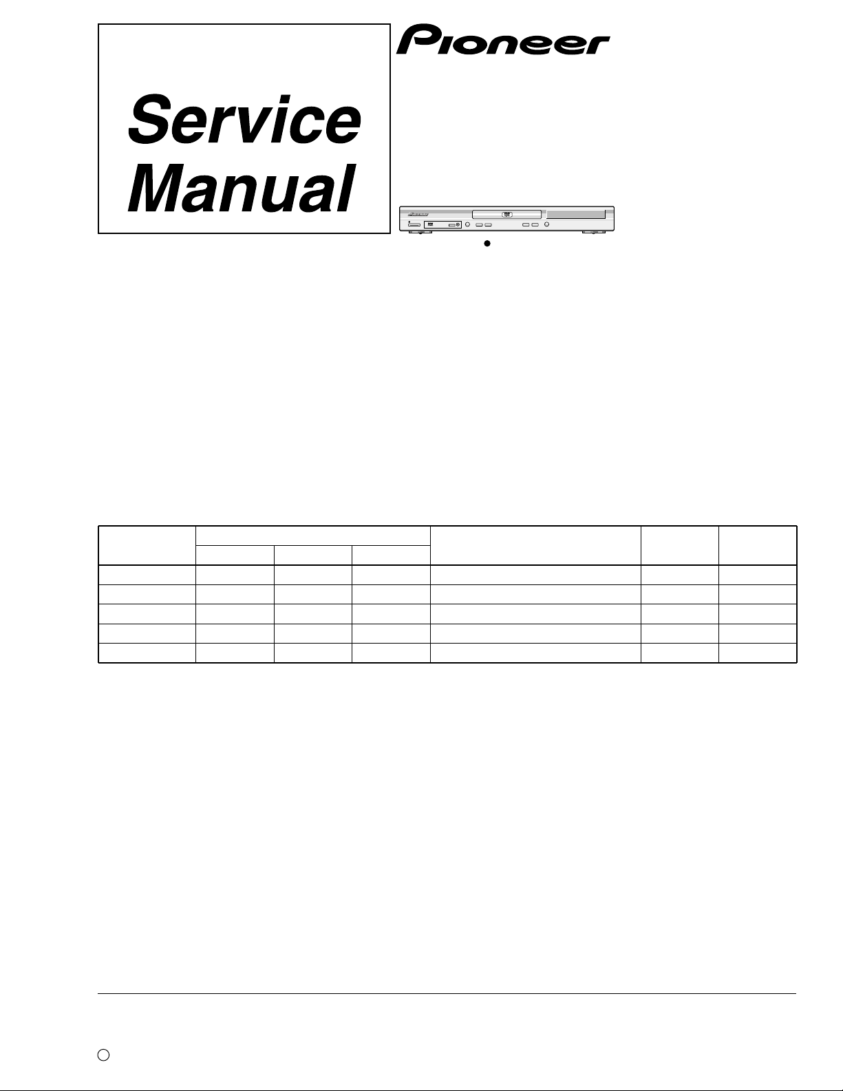
DV-545
8
7
3
STANDBY/ON
¡¢41
LEGATO
0
PRO
DVD PLAYER
DV-545
DV-444-S
DV-444-K
THIS MANUAL IS APPLICABLE TO THE FOLLOWING MODEL(S) AND TYPE(S).
Type
WYXJ ? −−AC220-240V 2
WVXJ ? −−AC220-240V 2
WYXQ − ??AC220-240V 2
WYXQ/FRGR − ??AC220-240V 2
WVXQ − ??AC220-240V 2
DV-545 DV-444-S DV-444-K
Model
Power Requirement Region No. Remarks
ORDER NO.
RRV2465
CONTENTS
1. SAFETY INFORMATION
2. EXPLODED VIEWS AND PARTS LIST
3. BLOCK DIAGRAM AND SCHEMATIC DIAGRAM
4. PCB CONNECTION DIAGRAM
5. PCB PARTS LIST
6. ADJUSTMENT
PIONEER CORPORATION 4-1, Meguro 1-chome, Meguro-ku, Tokyo 153-8654, Japan
PIONEER ELECTRONICS SERVICE, INC. P.O. Box 1760, Long Beach, CA 90801-1760, U.S.A.
PIONEER EUROPE NV Haven 1087, Keetberglaan 1, 9120 Melsele, Belgium
PIONEER ELECTRONICS ASIACENTRE PTE. LTD. 253 Alexandra Road, #04-01, Singapore 159936
c
PIONEER CORPORATION 2001
................................................
.....................................................
.......................................
.................
...
...........................
10
35
46
51
2
3
7. GENERAL INFORMATION
7.1 DIAGNOSIS
7.1.1 SELF-DIAGNOSTIC FUNCTION OF
PICKUP DEFECTIVE
7.1.2 TEST POINTS LOCATION
7.1.3 TEST MODE SCREEN DISPLAY
7.1.4 TROUBLE SHOOTING
7.1.5 ERROR CODE
7.1.6 DISASSEMBLY
7.2 PARTS
7.2.1 IC
7.2.2 FL DISPLAY
8. PANEL FACILITIES AND SPECIFICATIONS
..................................................
..........................................................
..........................................................
................................
...........................
...................
........................
.....................................
....................................
.........................................
T – IZE JUNE 2001 Printed in Japan
........
....
57
57
57
58
59
63
64
68
74
74
93
94
Page 2
DV-545, DV-444-S, DV-444-K
1. SAFETY INFORMATION
This service manual is intended for qualified service technicians ; it is not meant for the casual do-ityourselfer. Qualified technicians have the necessary test equipment and tools, and have been trained
to properly and safely repair complex products such as those covered by this manual.
Improperly performed repairs can adversely affect the safety and reliability of the product and may
void the warranty. If you are not qualified to perform the repair of this product properly and safely, you
should not risk trying to do so and refer the repair to a qualified service technician.
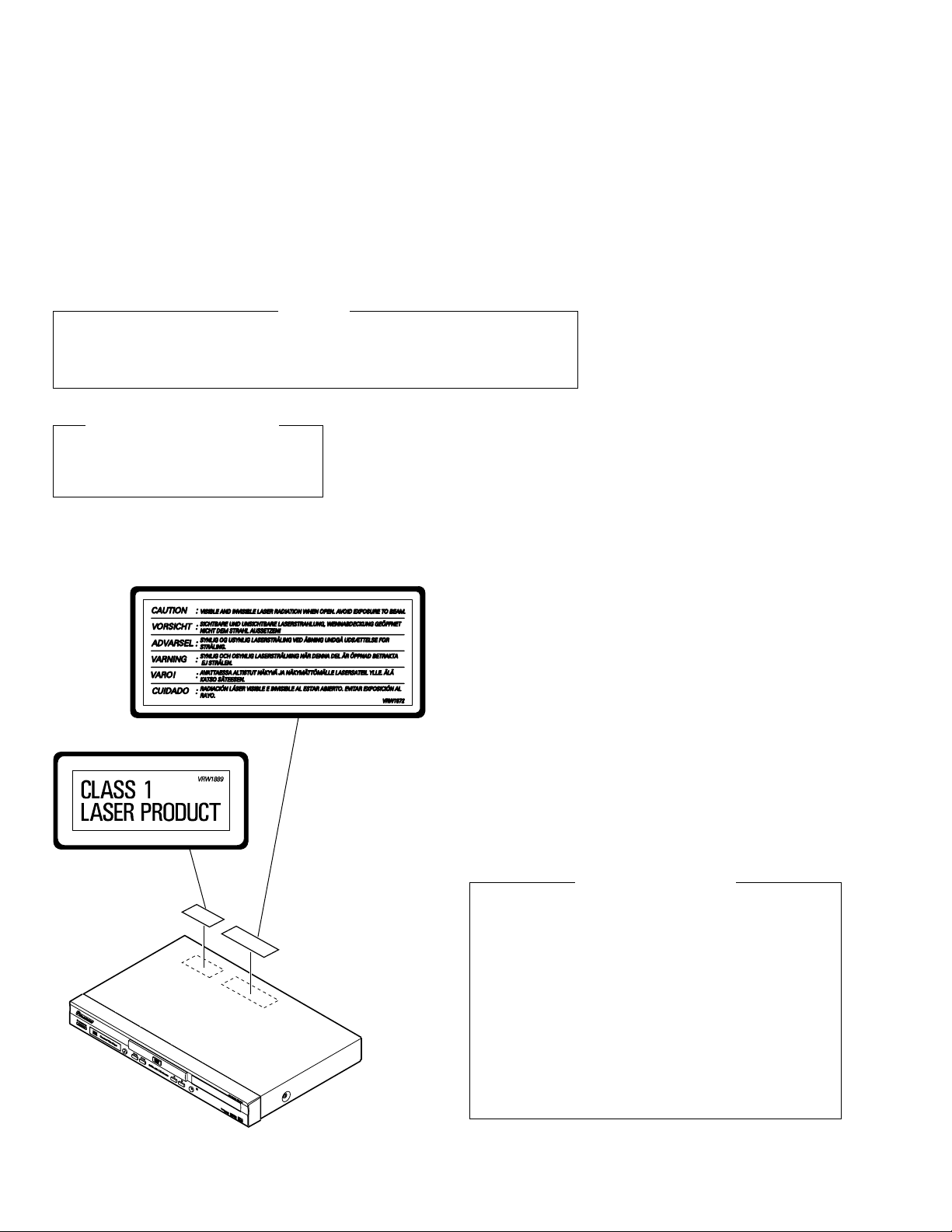
WARNING !
THE AEL (ACCESSIBLE EMISSION LEVEL) OF THE LASER POWER OUTPUT IS LESS THAN CLASS 1
BUT THE LASER COMPONENT IS CAPABLE OF EMITTING RADIATION EXCEEDING THE LIMIT FOR
CLASS 1.
A SPECIALLY INSTRUCTED PERSON SHOULD DO SERVICING OPERATION OF THE APPARATUS.
LASER DIODE CHARACTERISTICS
FOR DVD : MAXIMUM OUTPUT POWER : 5 mW
FOR CD : MAXIMUM OUTPUT POWER : 5 mW
WAVELENGTH : 650 nm
WAVELENGTH : 780 nm
LABEL CHECK
DV-545/WYXJ
Only
Additional Laser Caution
1. Loading-status detection switch (S101 on the LOAB assy) are detected
by the microprocessor (IC601 in the DVDM assy).
• To per mit the laser diode to oscillate, it is required to set the loadingstatus detection switch for the clamp position (the center terminal of S101
is shorted to +3V).
When the voltage of IC101-pin 20 is +3V and IC601 (microprocessor) pin 83 is +3V, 650nm laser diode for DVD oscillates in the DVDM Assy.
When the voltage of IC101-pin 20 is +3V and IC601 (microprocessor) pin 83 is 0V (GND), 780nm laser diode for CD oscillates in the DVDM
Assy.
In the test mode ∗ , the laser diode oscillates when microprocessor detects
a PLA Y signal, or when the PLAY key is pressed (S203 ON in the FLKB
assy), with the above requirements satisfied.
2. When the cover is open, close viewing through the objective lens with
the naked eye will cause exposure to the laser beam.
∗ : See page 53.
2
Page 3
DV-545, DV-444-S, DV-444-K
2. EXPLODED VIEWS AND PARTS LIST
NOTES:• Parts marked by "NSP" are generally unavailable because they are not in our Master Spare Parts List.
The mark found on some component parts indicates the importance of the safety factor of the part.
•
Therefore, when replacing, be sure to use parts of identical designation.
Screws adjacent to mark on the product are used for disassembly.
•
2.1 PACKING
6
2
3
1
Except
WVXJ and WVXQ
Types
18, 19
"Operating
Instructions"
14
WYXJ and WYXQ
Types Only
8
12
16, 17
"Operating
Instructions"
12
11
13
7 (1/2)
FRONT
WVXJ and WVXQ
Types Only
15
11
7 (2/2)
10
9
1
5
7 (2/2)
7 (1/2)
(1) PACKING PARTS LIST
Mark No. Description Part No.
1 Power Cord See Contrast table (2)
NSP 6 Dry Cell Battery (R6P, AA) See Contrast table (2)
NSP 8 Warranty Card ARY7022
4
NSP 11 Reinforcement Board VHC1083
NSP 13 Polyethylene Bag Z21-038
2 Audio Cord (L = 1.5m) See Contrast table (2)
3 Video Cord (L = 1.5m) See Contrast table (2)
4 Remote Control Unit See Contrast table (2)
5 Battery Cover See Contrast table (2)
7 Pad VHA1277
9 Packing Case See Contrast table (2)
10 Mirror Mat (0.5 × 750 × 600) Z23-007
12 Polyethylene Bag VHL1051
(0.03 × 200 × 300)
(0.03 × 230 × 340)
14 IM Holder See Contrast table (2)
15 Accessory Box See Contrast table (2)
16 Operating Instructions See Contrast table (2)
17 Operating Instructions See Contrast table (2)
18 Operating Instructions See Contrast table (2)
19 Operating Instructions See Contrast table (2)
(2) CONTRAST TABLE
DV-545/WYXJ, WVXJ, DV-444-S/WYXQ, WYXQ/FRGR, WVXQ, DV-444-K/WYXQ, WYXQ/FRGR and WVXQ are constructed
the same except for the following :
Part No.
Mark No. Symbol and Description
1
Power Cord
2
Audio Cord (L = 1.5m)
3
Video Cord (L = 1.5m)
4
Remote Control Unit
5
Battery Cover
NSP
6
Dry Cell Battery (R6P, AA)
9
Packing Case
14
IM Holder
15
Accessory Box
16
Operating Instructions (English/Italian)
17
Operating Instructions
18
Operating Instructions
19
Operating Instructions
(French/German)
(Dutch/Swedish)
(Spanish/Portuguese)
DV-545 DV-444-S DV-444-K
WYXJ WVXJ WYXQ
ADG1154
VDE1052
VDE1053
VXX2627
VNK4423
VEM-013
VHG2121
VHC1082
Not used
VRD1132
VRD1133
VRD1134
VRD1135
ADG1156
VDE1052
VDE1053
VXX2627
VNK4423
VEM-013
VHG2096
Not used
VHC1080
VRD1132
Not used
Not used
Not used
ADG1154
VDE1054
VDE1055
VXX2702
VNK4631
VEM1010
VHG2083
VHC1082
Not used
VRD1137
VRD1138
VRD1139
VRD1140
WYXQ
/FRGR
ADG1154
VDE1054
VDE1055
VXX2702
VNK4631
VEM1010
VHG2102
Not used
Not used
Not used
VRD1138
Not used
Not used
WVXQ WYXQ
ADG1156
VDE1054
VDE1055
VXX2702
VNK4631
VEM1010
VHG2103
Not used
VHC1080
VRD1137
Not used
Not used
Not used
ADG1154
VDE1054
VDE1055
VXX2702
VNK4631
VEM1010
VHG2080
VHC1082
Not used
VRD1137
VRD1138
VRD1139
VRD1140
WYXQ
/FRGR
ADG1154
VDE1054
VDE1055
VXX2702
VNK4631
VEM1010
VHG2100
Not used
Not used
Not used
VRD1138
Not used
Not used
WVXQ
ADG1156
VDE1054
VDE1055
VXX2702
VNK4631
VEM1010
VHG2101
Not used
VHC1080
VRD1137
Not used
Not used
Not used
3
Page 4
DV-545, DV-444-S, DV-444-K
2.2 EXTERIOR SECTION
29
18
DV-545 Only
33
32
28
Refer to
"2.3 LOADING MECHANISM ASSY".
2
27
17
28
28
C
27
F
D
E
16
3
27
28
E
7
28
29
DV-545
Only
28
19
28
28
H
C
15
8
14
D
A
B
27
26
24
4
13
F
E
C
11
B
27
1
25
20
21
23
6
G
30
31
30
30
DV-545
Only
30
30
30
30
30
D
10
B
11
30
30
F
5
A
9
24
21
30
22
30
12
4
Page 5
(1) EXTERIOR SECTION PARTS LIST
DV-545, DV-444-S, DV-444-K
Mark No. Description Part No.
NSP 2 Loading Mechanism Assy VWT1188
NSP 3 SSIB Assy VWG2292
NSP 5 FLKB Assy See Contrast table (2)
NSP 6 KEYB Assy See Contrast table (2)
NSP 14 PCB Support REC1285
NSP 17 Base Chassis VNA2300
1 DVDM Assy See Contrast table (2)
4 JACB Assy See Contrast table (2)
7 SRCB Assy See Contrast table (2)
8 POWER SUPPLY Unit VWR1340
9 Flexible Cable (16P) See Contrast table (2)
10 Flexible Cable (17P) See Contrast table (2)
11 Flexible Cable (30P) See Contrast table (2)
12 Leg Assy SX AEC7113
13 Connector Assy PG05KK-E30
15 PCB Support VEC2184
16 Rear Panel See Contrast table (2)
18 Bonnet See Contrast table (2)
19 Flexible Cable (19P) See Contrast table (2)
20 DVD-V Plate See Contrast table (2)
Mark No. Description Part No.
21 Rubber Foot VEB1325
22 FP Angle VNE2250
23 Tray Panel See Contrast table (2)
24 Ring VNK4840
25 Front Panel Assy See Contrast table (2)
26 Pioneer Name Plate See Contrast table (2)
27 Screw BBZ30P060FMC
28 Screw BBZ30P080FZK
29 Screw See Contrast table (2)
30 Screw BBZ30P100FZK
31 LED Lens See Contrast table (2)
32 Label VRW1872
33 CLASS 1 Caution Label See Contrast table (2)
(2) CONTRAST TABLE
DV-545/WYXJ, WVXJ, DV-444-S/WYXQ, WYXQ/FRGR, WVXQ, DV-444-K/WYXQ, WYXQ/FRGR and WVXQ are constructed
the same except for the following :
Part No.
DV-545 DV-444-S DV-444-K
Mark No. Symbol and Description
1
DVDM Assy
4
NSP
NSP
JACB Assy
5
FLKB Assy
6
KEYB Assy
7
SRCB Assy
WYXJ,
WVXJ
VWS1488
VWV1843
VWG2283
VWG2291
VWV1848
WYXQ,
WYXQ/FRGR,
WVXQ
VWS1487
VWV1842
VWG2282
VWG2290
VWV1847
WYXQ,
WYXQ/FRGR,
WVXQ
VWS1487
VWV1842
VWG2282
VWG2290
VWV1847
Remarks
NSP
9
Flexible Cable (16P)
10
Flexible Cable (17P)
11
Flexible Cable (30P)
16
Rear Panel
18
Bonnet S
18
Bonnet
19
Flexible Cable (19P)
20
DVD-V Plate
23
Tray Panel
25
Front Panel Assy
26
Pioneer Name Plate
29
Screw
31
LED Lens
33
CLASS 1 Caution Label
VDA1860
VDA1862
VDA1871
VNA2294
VXX2773
Not used
VDA1866
VAM1120
VNK4837
VXA2477
VAM1129
BCZ40P060FNI
VNK4841
VRW1889
VDA1861
VDA1863
VDA1872
VNA2344
Not used
VNA2333
VDA1867
VAM1121
VNK4837
VXA2469
VAM1129
BCZ40P060FNI
Not used
Not used
VDA1861
VDA1863
VDA1872
VNA2342
Not used
VNA2331
VDA1867
VAM1121
VNK4835
VXA2466
VAM1109
BCZ40P060FZK
Not used
Not used
5
Page 6
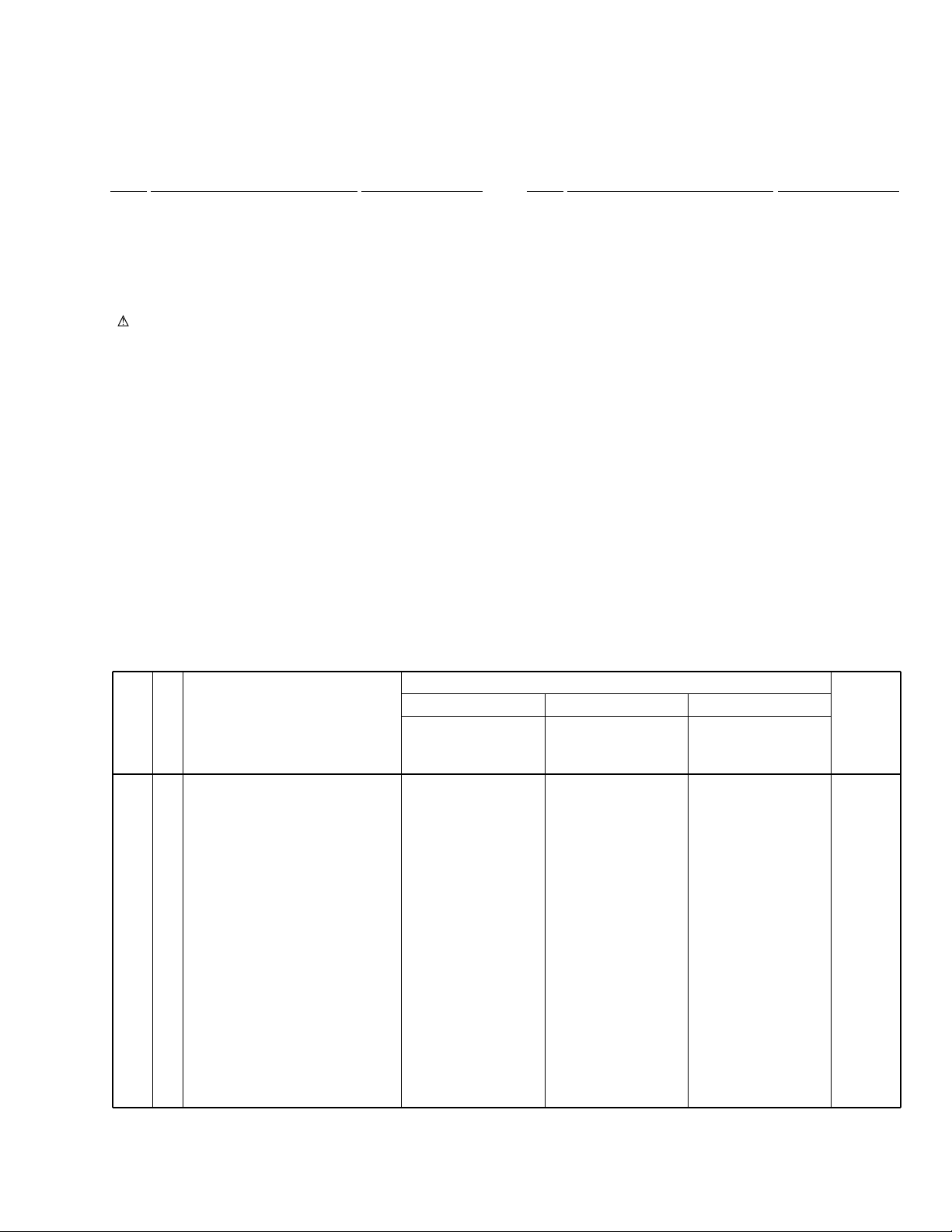
DV-545, DV-444-S, DV-444-K
2.3 LOADING MECHANISM ASSY
Note :
Refer to
" Apply Position of Lubricant".
Daifree
GEM1036
2
Refer to
"2.4 TRAVERSE MECHANISM
6
To DVDM
CN151
8
8
ASSY-S".
8
23
15
14
12
Lubricating Oil
GYA1001
13
22
9
22 22
16
8
20
3
17
21
7
A
11
1
A
A
4
5
22
10
Lubricating Oil
GYA1001
18
22
19
LOADING MECHANISM ASSY PARTS LIST
•
Mark No. Description Part No.
NSP 1 LOAB Assy VWG2279
2 Traverse Mechanism Assy-S VXX2782
3 Loading Motor Assy VXX2505
4 Motor Pulley PNW1634
5 Carriage DC Motor / 0.3W PXM1027
6 Flexible Cable (26P) VDA1864
7 Connector Assy 2P VKP2253
8 Float Rubber VEB1327
9 Belt VEB1330
10 Stabilizer VNE2253
6
Mark No. Description Part No.
11 Loading Base VNL1917
12 Float Base DVD VNL1918
13 Drive Cam VNL1919
14 Gear Pulley VNL1921
15 Loading Gear VNL1922
16 Drive Gear VNL1923
17 SW Lever VNL1925
18 Clamper Plate VNE2251
19 Bridge VNE2252
20 Clamper VNL1924
21 Screw JGZ17P028FMC
22 Screw Z39-019
23 Tray VNL1920
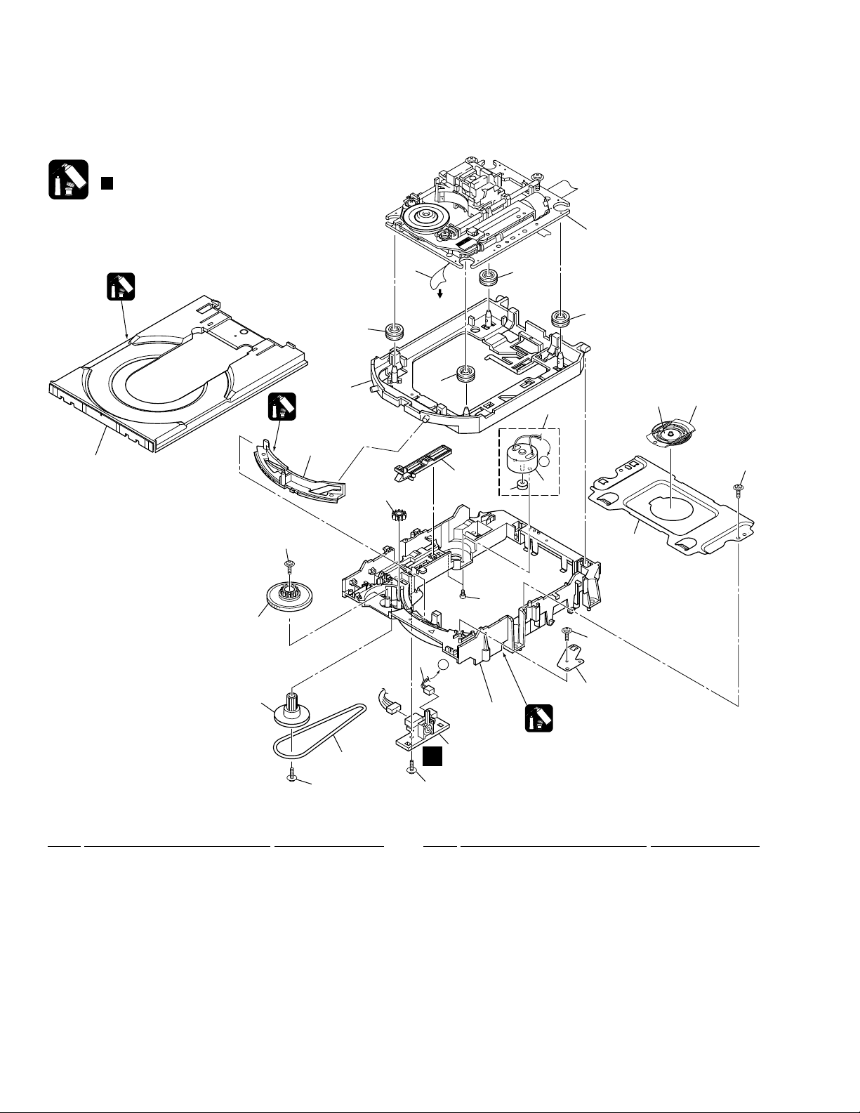
Page 7
Apply Position of Lubricant
No. 11
Loading Base
DV-545, DV-444-S, DV-444-K
Lubricating Oil
GYA1001
Around the shaft
Lubricating Oil
GYA1001
Rear View
No. 23
Tray
No. 13
Drive Cam
Inner side of a ditch
Lubricating Oil
GYA1001
Inner side of a ditch
Lubricating Oil
GYA1001
Daifree
GEM1036
Concave of unevenness
Top View
No. 23
Tray
Lubricating Oil
GYA1001
Lubricating Oil
GYA1001
No. 13
Drive Cam
Daifree
GEM1036
Concave of unevenness
Top View
Concave of unevenness
Daifree
GEM1036
Bottom View
Inner side of a ditch
Daifree
GEM1036
Side of the rib
Daifree
GEM1036
7
Page 8
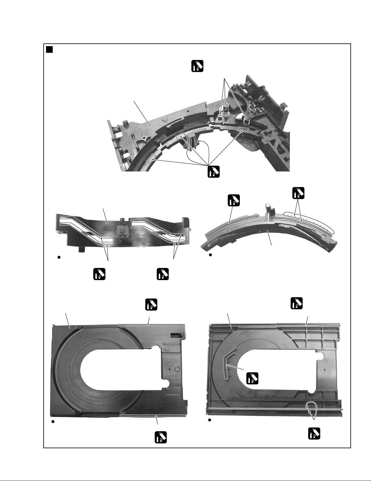
DV-545, DV-444-S, DV-444-K
2.4 TRAVERSE MECHANISM ASSY-S
17 (Torque : 0.12 ± 0.01 N•m)
13
18
10
1
16
18
18
10
12
8
7
6
19
4 (Adjustment Screw)
4 (Adjustment Screw)
5
5
Screw Tight
GYL1001
17 (Torque : 0.12 ± 0.01 N•m)
Silicone Adhesive
GEM1037
3
14
9
Silicone Adhesive
GEM1037
17
(Torque : 0.12 ± 0.01 N•m)
15
Silicone Adhesive
GEM1037
11
TRAVERSE MECHANISM ASSY-S PARTS LIST
•
Mark No. Description Part No.
1 Spindle Motor VXM1088
2 Stepping Motor VXM1090
(CARRIAGE) (or VXM1091)
3 Pickup Assy-S OXX8003
4 Skew Screw VBA1080
5 Skew Spring VBH1335
6 Guide Bar VLL1514
7 Sub Guide Bar VLL1515
8 Hold Spring VNC1017
(or VXM1089)
16
2
Mark No. Description Part No.
9 Joint Spring VNC1019
10 Support Spring VNC1020
NSP 11 Mechanism Chassis VNE2248
12 Slider VNL1811
13 Spacer VNL1913
14 Joint VNL1914
15 FFC Holder VNL1915
16 Screw BBZ20P050FZK
17 Screw OBA8009
18 Screw PMA26P100FMC
19 Damper Sheet VEB1335
8
Page 9

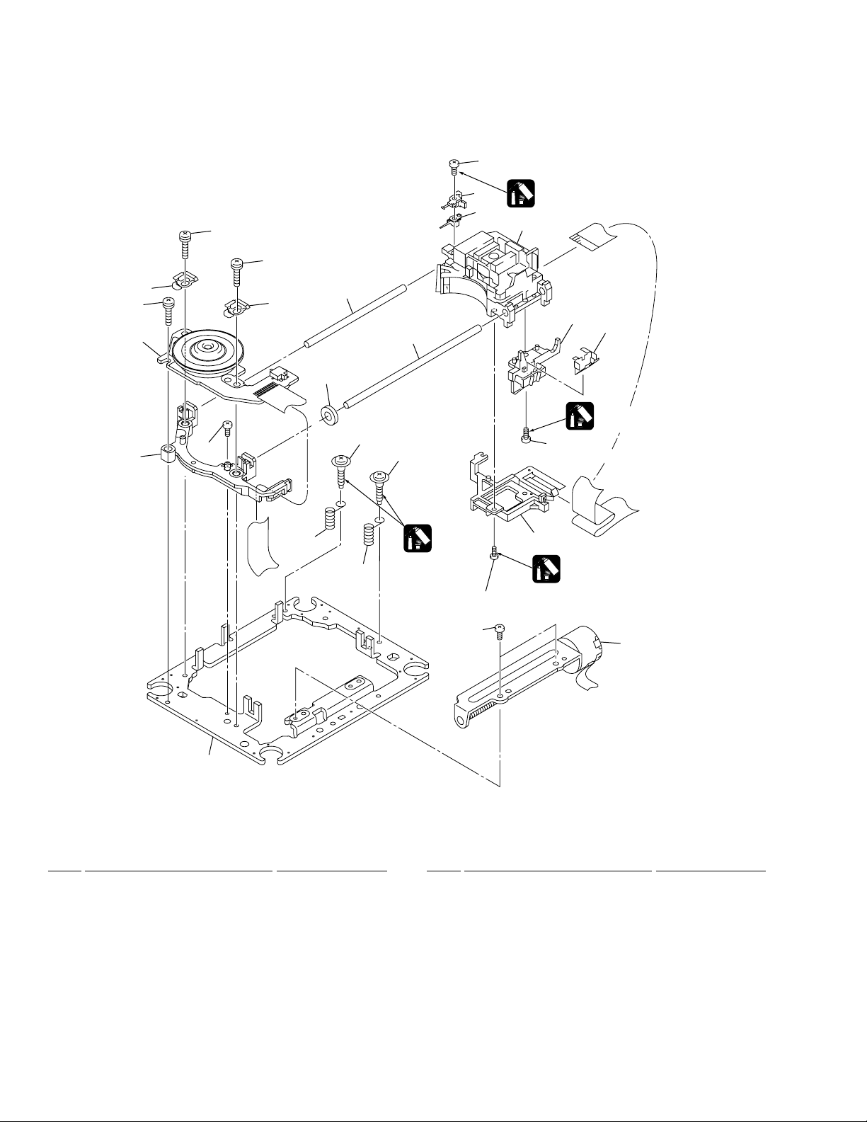
DV-545, DV-444-S, DV-444-K
9
Page 10
1
23
DV-545, DV-444-S, DV-444-K
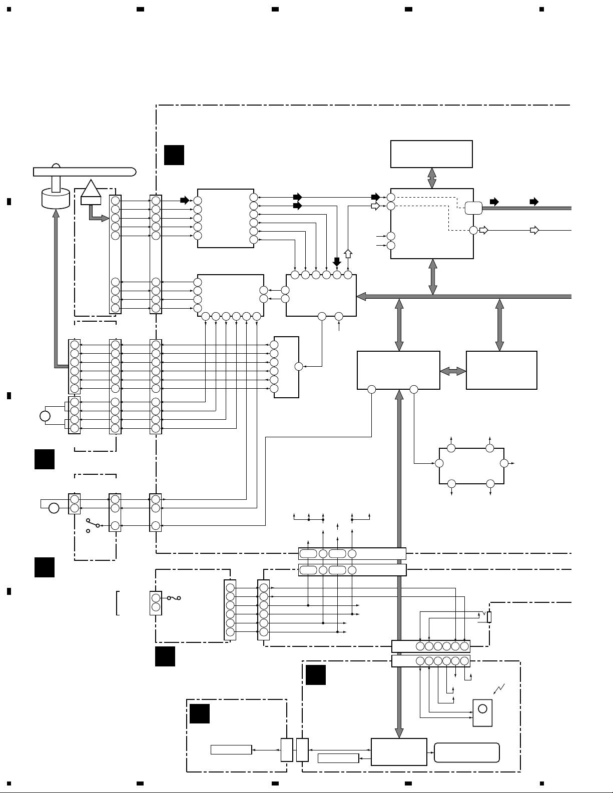
3. BLOCK DIAGRAM AND SCHEMATIC DIAGRAM
3.1 BLOCK DIAGRAM
A
DVDM ASSY
B
4
IC712
MSM51V17805D-60TS
16M DRAM
CN151
(26P)
RF
B1
B2
B3
B4
(RF)
RF
16
7
6
12
11
3
B1
B2
B3
B4
6
LA9701M
7
8
9
IC101
RF IC
54
46
56
57
42
35
Spindle
Motor
PICKUP
(26P)
11
20
21
15
16
ASSY
T DRV
25
T RTN
24
F DRV
S101
Loading
Position
Switch
CN601
AC IN
23
F RTN
26
CN3
(17P)
H1+
9
H1-
10
H2+
11
H2-
12
H3+
13
H3-
14
ST1+
1
ST1-
2
ST2+
4
ST2-
5
(5P)
LOD- LOD-
1
LOD+ LOD+
2
SW2 LODPOS
4
LIVE
NEUTRAL
B
CN1
(12P)
9
8
7
6
5
4
3
M
Stepping
Motor
(Carriage)
C
C
A
4
2
1
CN2
(4P)
SSIB ASSY
CN602
(2P)
2
+-
1
M
Loading
Motor
Assy
LOAB ASSY
2
3
4
1
9
10
11
12
13
14
1
2
4
5
1
2
4
1
2
CN61
(17P)
CN51
(5P)
CN1
(2P)
T DRV
T RTN
F DRV
F RTN
F1
12
IC351
13
M56788AFP
9
FTS Driver
10
35 34 31 32 15 14
CN101
(14P)
14
10
8
6
4
2
-27V
EV+5V
+6V
+12V
+5V
+3.3V
POWER
H
SUPPLY
UNIT
D
KEYB ASSY
G
KEY SW
10
(RF) (RF)
RFO
DSP RF
(RF)
BH
PH
FE
TE
32 33 30 31 39 3
FDO
47
3
TDO
48
20
9
10
11
12
13
14
IC201
LC78652W
Servo DSP IC
SPDO
21
IC251
BA6664FM
Spindle
Driver
V+5VV+5S
SW+5
V+6M
28,30 21,23
1,3 8,10
-27V
EV+5V
1
5
7
9
11
13
CN101
(14P)
F
CN201
(4P)
CN102
(4P)
(RF)
46 14
16M
V+5D
V+3D
V3VD
29 22
2
FLKB
ASSY
KEY SW
ROMXA
(AD)
33M
16M
(AD)
System Control
57
LODPOS
V+12D V+12M
V12M
9
V+6M
V+12V
V+5V
V+3V
CN104
CN101
170
112
PE5108A
4
DVD Decoder
107
BY Chip
IC601
PD6345A
105
X48/44
X48/44
CONTROLCONTROLCONTROL
CN31 (2/2)
CN102 (2/2)
(16P)
(16P)
IC101
PE5251A
FL Control IC
IC701
27M
(for IC801)
3
IC481
14 15
BU2288FV
Clock Generator
10
22/24M
(for IC211)
(30P)
(30P)
IR
SEL IR
16
1
SEL IR
15
5
2
12116314215
IR
-27V
-27V
FLAC2
FLAC1
V101 VAW1063
FL Tube
(VD) (VD)
57-60
63-66
111
SD0-SD7
CDDATA
IC603
VYW1852
8M Flash Memory
16M
(for IC201, IC701)
13
33M
(for IC701)
9
36/16M
(for IC801)
JA150
CONTROL
EV+5V
E+5V
IR101
Remote
Receiver
Unit
1234
Page 11
5
678
DV-545, DV-444-S, DV-444-K
(RF)
(AD)
IC805
MB81F161622C-80FN
16M SDRAM
(VD)
149,150,
152-155,
158,159
48
IC801
M65774BFP
MPEG2 Decoder
AV-1
5564
27M36/16M
: RF SIGNAL ROUTE
: AUDIO DATA SIGNAL ROUTE
: AUDIO SIGNAL ROUTE
(D)
: AUDIO (DIGITAL) SIGNAL ROUTE
(D)
(D)
DOUT0
74
ADA0A
68
PD0-PD7
95-98,
100-103
(VD)
93
27M
(VD)
(VD)
2-9
27M
48
IC861
ADV7172KST
Video Encoder
DV-545 Only
IC807
PD0274A
AQE
Cr/R
24
Y/G
28
Cb/B
25
V
35
Y
33
C
29
(VD)
: VIDEO DATA SIGNAL ROUTE
: VIDEO SIGNAL ROUTE
(V)
: V SIGNAL ROUTE
(Y)
: Y SIGNAL ROUTE
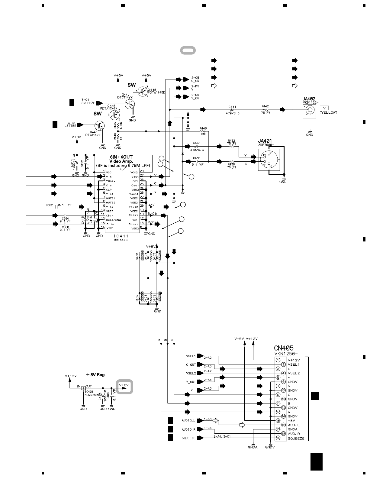
CN31 (1/2)
(30P)
DOUT0
(D) (D) (D)
5 26
DOUT
CN102 (1/2)
(30P)
(C)
: C SIGNAL ROUTE
(R)
: R SIGNAL ROUTE
(G)
: G SIGNAL ROUTE
(B)
: B SIGNAL ROUTE
IC211
PCM1742KE
CN106
7
2
29
27
25
26
30
28
(30P)
22/24M
192kHz, 24bit
2ch DAC
2
16
(R)
Cr/R
Y/G
(Y)
Cb/B
(B)
V
(V)
(Y)
Y
C
(C)
7
8
13
9
11
2
6
4
2828
Q912
Q901
Q903
22/24M
Q911
Q913
Q902
CN32
(30P)
7
2
29
27
25
26
30
28
ADATA0
Cr/R
Y/G
Cb/B
V
Y
C
IC411
MM1540BF
6ch Amp.
Driver with LPF
IC231
BA4560F
(V)
V
27
(Y)
Y
23
C
(C)
25
Cr/R
16
Y/G
20
Cb/B
18
(D)
Q601
(D)
(Y)
Y
C
(C)
AUDIO_L
AUDIO_R
(R)
(G)
(B)
V
C
Y
R
G
B
JA601
JA602
JA201
JA401
JA402
7
3
5
16
18
13
9
11
CN405
OPTICAL
DIGITAL
COAXIAL
L
AUDIO
R
S VIDEO
V
COMPOSITE
(19P)
A
B
C
CN701
(19P)
AUDIO_L
AUDIO_R
2
V
(V)
13
(Y) (Y)
Y
15
(C)
C
17
7
11
9
E
6
(R)
R
4
(G)
G
(B)
B
IC802
MM1505XN
SRCB ASSY
2
DV-545 Only
5
6
Relay
(V)
RY801
4
6
(R/C)
(V) (V)
(G)
(B)
DV-545 Only
IC801
MM1507XN
2
Relay
Relay
Relay
RY702
RY803
RY802
DV-545 Only
DV-545
Only
DV-545
Only
7
Relay
RY701
(V/Y)
(R/C)
(G)
(B)
JA701
(21P)
L OUT
34
R OUT
1
(V/Y)
V/Y OUT
19
R/C OUT
15
(R/C)
(B)
(V)
(G)
JA702
(21P)
G OUT
11
B OUT
7
DV-545
L OUT
3
Only
R OUT
1
V OUT
19
D
11
8
Page 12
1
23
DV-545, DV-444-S, DV-444-K
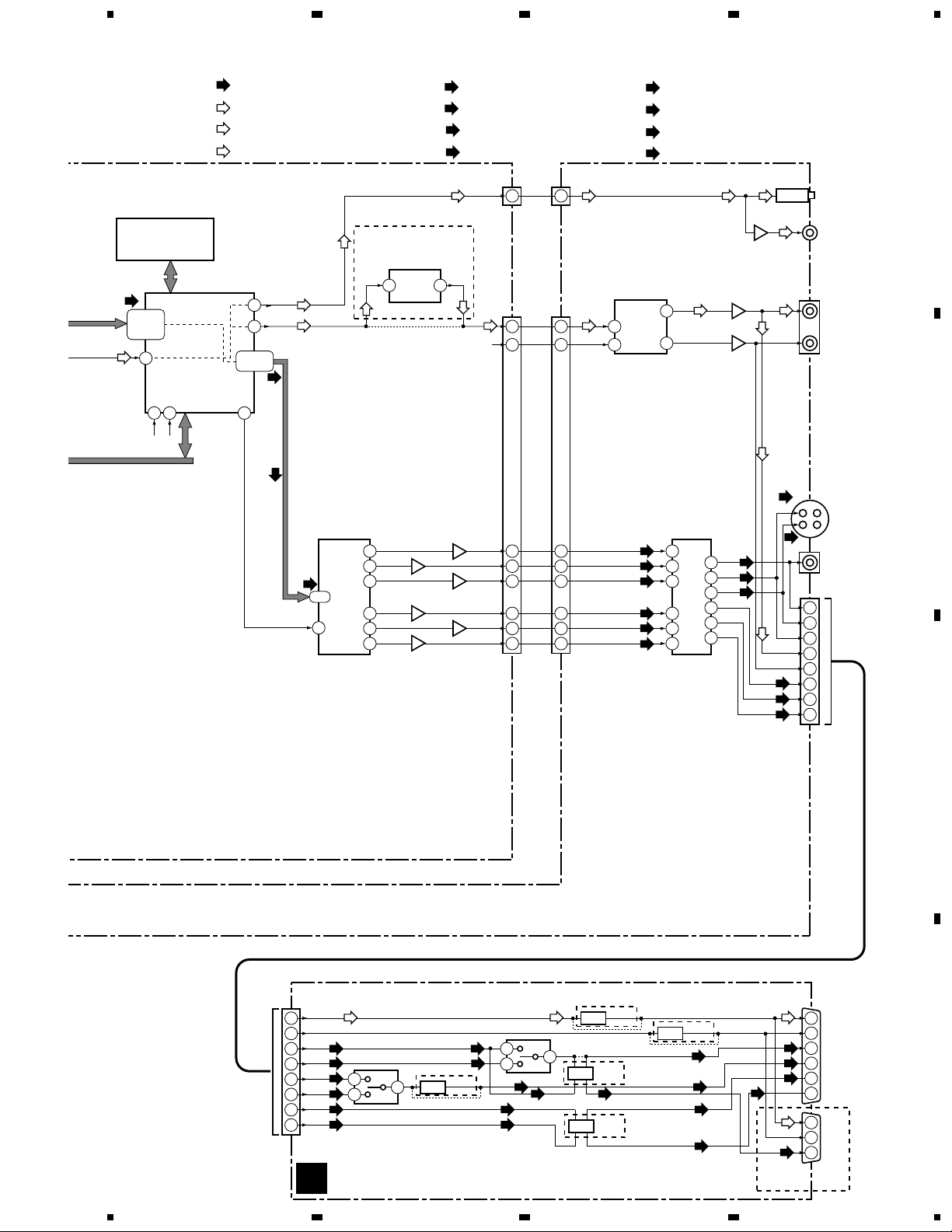
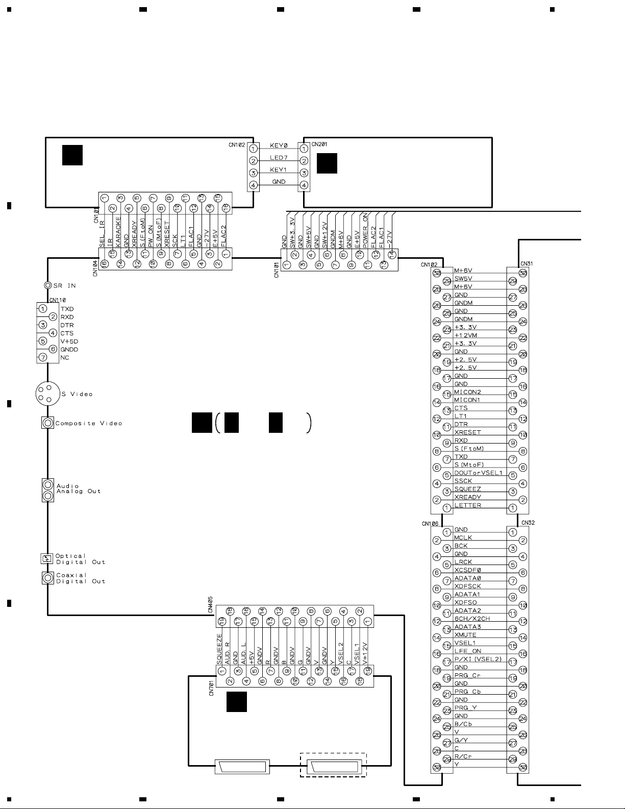
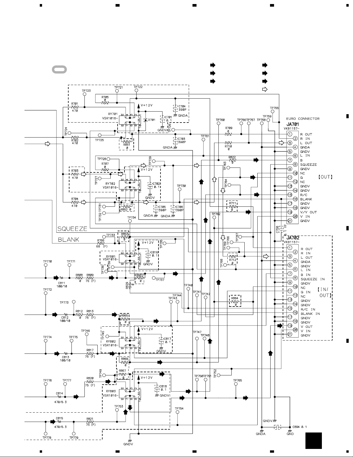
3.2 LOAB, SSIB ASSYS and OVERALL WIRING DIAGRAM
A
4
FLKB ASSY
F
(DV-545 : VWG2283)
(DV-444-S, K : VWG2282)
B
D
D 1/3- D 3/3
KEYB ASSY
G
(DV-545 : VWG2291)
(DV-444-S, K : VWG2290)
JACB ASSY
(DV-545 : VWV1843)
(DV-444-S, K : VWV1842)
C
D
E
SRCB ASSY
(DV-545 : VWV1848)
(DV-444-S, K : VWV1847)
JA702JA701
12
1234
DV-545 ONLY
Page 13
5
678
DV-545, DV-444-S, DV-444-K
Note : When ordering service parts, be sure to refer to "EXPLODED VIEWS and PARTS LIST" or "PCB PARTS LIST".
(RF)
: RF SIGNAL ROUTE
(F)
: FOCUS SERVO LOOP LINE
(T)
: TRACKING SERVO LOOP LINE
(S)
H
POWER SUPPLY
UNIT
(VWR1340)
PICKUP ASSY-S (OXX8003)
: SLIDER SERVO LOOP LINE
POWER CORD
WYXJ, WYXQ, WYXQ/FR/GR : ADG1154
WVXJ, WVXQ : ADG1156
AC110-127V, 220-240V
50/60Hz
A
B
B 1/4- B 4/4
B
DVDM ASSY
(DV-545 : VWS1488)
(DV-444-S, K : VWS1487)
(RF) (RF) (RF) (RF)
(F)
(F)
(T)
(T)
(F)
(F)
(F)
(T)
(T)
(F)
VKN1272
(S)
(S)
(S)
(S)
(S)
(S)
(S)
(S)
CN3
VKN1277
SSIB ASSY
C
(VWG2292)
VKN1264
CN1
(F)
(T)
(T)
(F)
CN2
(F)
(F)
(T)
(T)
(F)
(F)
(F)
(T)
(T)
(F)
STEPPING MOTOR
(CARRIAGE)
: VXM1090
SPINDLE MOTOR
: VXM1088
C
S101
: VSK1011
D
CN602
S2B-PH-K
CN601
S5B-PH-K
LOAB ASSY (VWG2279)
A
5
6
7
LOADING
MOTOR
ASSY
: VXX2505
CA
13
8
Page 14
1
23
DV-545, DV-444-S, DV-444-K
4
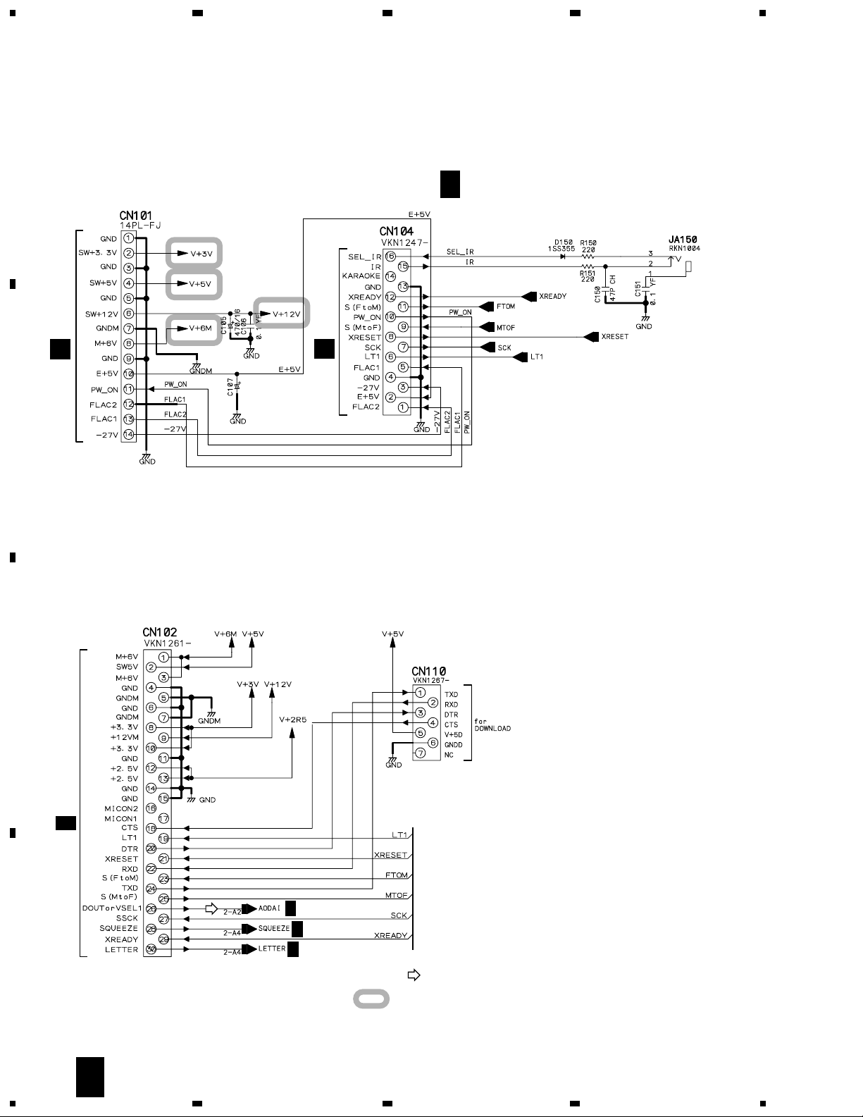
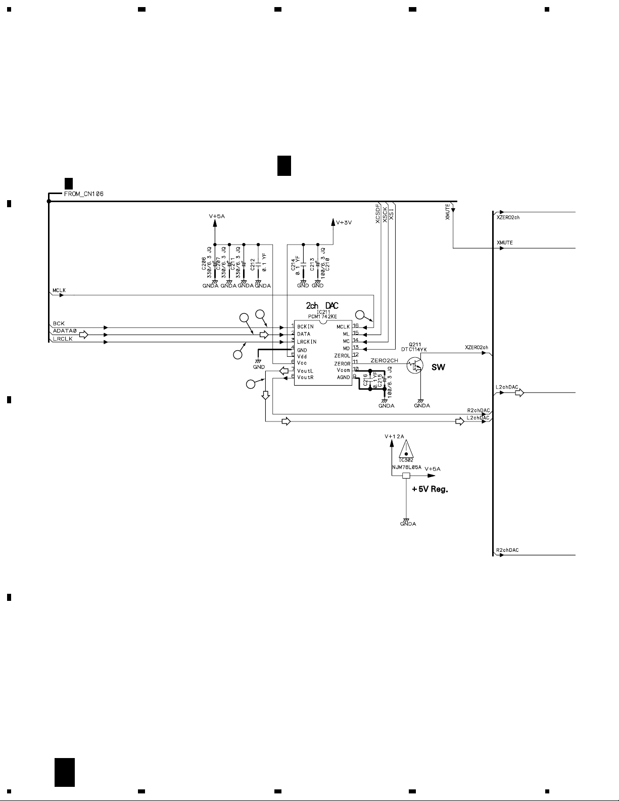
3.3 DVDM ASSY (1/4)
2/4
B
A
B
B 1/4
DVDM ASSY
(DV-545 : VWS1488)
(DV-444-S, K : VWS1487)
(V) (V)
1
(RF)
(RF)
B
2/4
(F)
(T)
(T)
(V)
(V)
(F)
(A)
(F)
B
2/4
2
(A)
(T)
(A)
(F)
(T)
DV-545
ONLY
B
B
DV-444-S, K
ONLY
4
2/4
2/4
B
2/4
DV-444-S, K
ONLY
B
2/4
C
(RF)
(F)
(F)
PICKUP ASSY
(T)
(T)
(F)
(F)
2/4
B
(F)
(T)
(T)
(F)
DV-545
ONLY
B
2/4,3/4
B
2/4
(S)
DV-545
ONLY
(S)
A
CN601
D
B
2/4
(F)
(T)(T)
(F)
(F)
(T)(T)
(T)
C
CN3
14
(F)
(F)
(F)
1/4
B
1234
(T)
Page 15
5
678
DV-545, DV-444-S, DV-444-K
DV-444-S,K
ONLY
B
(V)
3/4
DV-545
ONLY
DV-545
ONLY
R332
DV-545 : 470
DV-444-S, K : 330
IC304
R336
DV-545 : 100k
DV-444-S, K : 0
C322
DV-545 : 0.01
DV-444-S, K : 18p
R328
DV-545 : 1k
IC304
DV-545 : TC7SZU04F
DV-444-S, K : TC7SHU04F
R336
DV-545 : 3.3k
DV-444-S, K : 2.2k
DV-444-S, K : 1.8k
DV-545
ONLY
C314
DV-545 : 15p
DV-444-S, K : 22p
R314
DV-545 : 22k
DV-444-S, K : 10k
(V) (V)
R310
DV-545 : 82k
DV-444-S, K : 47k
R312
DV-545 : 10k
DV-444-S, K : 15k
2/4
B
B
3/4
(RF)
: RF SIGNAL ROUTE
(V)
: RF (VIDEO) SIGNAL ROUTE
(A)
: RF (AUDIO) SIGNAL ROUTE
(AD)
: AUDIO DATA SIGNAL ROUTE
(F)
: FOCUS SERVO LOOP LINE
(T)
: TRACKING SERVO LOOP LINE
(S)
: SLIDER SERVO LOOP LINE
DV-444-S, K
ONLY
DV-545 : 10k
FV-444-S, K : 33k
A
B
6
B
2/4
(AD)
3/4
B
(T)
(F)
(A)
(F)
(T)
B
2/4
(T)
(F)
5
(A)
(F)
(T)
B
3/4
B
2/4,3/4
C
8 9
7
B
2/4
B
3/4
1110
D
B
3/4
1/4
B
5
6
7
8
15
Page 16
1
23
DV-545, DV-444-S, DV-444-K
3.4 DVDM ASSY (2/4)
4
A
B 2/4
DVDM ASSY
(DV-545 : VWS1488)
(DV-444-S, K : VWS1487)
VYW1852
3/4
B
1/4
B
1/4
B
1/4,3/4
B
1/4
B
B
1/4
B
3/4
B
3/4
B
B
1/4
C
B
1/4
D
B
1/4
B
4/4
SH5
4/4
B
4/4
B
B
1/4
4/4
B
SH5
16
2/4
B
1234
Page 17
5
678
DV-545, DV-444-S, DV-444-K
VTL1078
B
3/4
B
4/4
B
3/4
B
3/4
B
3/4
B
1/4
B
B
3/4
1/4
(D)
: AUDIO (DIGITAL) SIGNAL ROUTE
A
B
1/4
B
C
D 1/3
CN102
(D)
(D)
B
3/4
B
3/4
: The power supply is shown with the marked box.
5
6
7
(D)
B
2/4
8
D
17
Page 18
1
DV-545, DV-444-S, DV-444-K
3.5 DVDM ASSY (3/4)
A
23
4
DV-444-S, K
ONLY
DV-545
ONLY
DV-444-S, K
ONLY
DV-545
ONLY
B
DV-444-S, K
ONLY
DV-545
ONLY
DV-545 : 220/4
DV-444-S, K : 100/16
IC712
DV-545 : MSM51V17805D-60TS
DV-444-S, K : MNR4800DJ7
B 3/4
DVDM ASSY
(DV-545 : VWS1488)
(DV-444-S, K : VWS1487)
B
1/4
DV-545 ONLY
B
DV-444-S, K
ONLY
B
2/4
1/4
B
4/4
B
BY-5
2/4
2/4
B
(VD)
(VD)
(V)
B
1/4
B
1/4
B
B
2/4
C
B
2/4
(AD)
B
2/4
B
2/4
(AD)
D
B
2/4
B
1/4
18
3/4
B
1234
(V)(V)
1/4
B
1/4
B
2/4
B
1/4
B
1/4
Page 19
5
678
DV-545, DV-444-S, DV-444-K
A
(V)
: RF (VIDEO) SIGNAL ROUTE
(VD)
: VIDEO DATA SIGNAL ROUTE
(AD)
: AUDIO DATASIGNAL ROUTE
: AUDIO SIGNAL ROUTE
(D)
: AUDIO (DIGITAL) SIGNAL ROUTE
(VD)
(VD) (VD)
(D)
B
B
2/4
4/4
B
(VD)
(D)
4/4
B
B
2/4
C
B
2/4
B
2/4
D
B
2/4
3/4
B
5
6
7
8
19
Page 20
1
DV-545, DV-444-S, DV-444-K
3.6 DVDM ASSY (4/4)
A
B
23
4
(V) (V)
B
3/4
2/4
B
C
(V)
(Y)
(C)
(V)
(VD) (VD)
D
(Y)
(C)
(R)
(B)
(Y)
(C) (C)
(Y)
(R)
(G)(G)
(B)
20
B
2/4
4/4
B
1234
Page 21
5
678
DV-545, DV-444-S, DV-444-K
B 4/4
DVDM ASSY
(DV-545 : VWS1488)
(DV-444-S, K : VWS1487)
(VD)
: VIDEO DATASIGNAL ROUTE
(V)
: V SIGNAL ROUTE
(Y)
: Y SIGNAL ROUTE
(C)
: C SIGNAL ROUTE
(R)
: R SIGNAL ROUTE
(G)
: G SIGNAL ROUTE
(B)
: B SIGNAL ROUTE
: AUDIO SIGNAL ROUTE
3/4
B
B
2/4
DV-545 ONLY
PD0274A
A
B
IC807
(AQE)
(V)
(V)
(Y) (Y)
(C)
(R)
(G)
(G)
(B)
(R)
(R)
DV-444-S, K
B
2/4
B
3/4
B
(R)
(G)
3/4
(Y)
(C)
(V)
(B)
(R)
(G)
(V)
(G)
ONLY
(Y)
(C)
(V)
(B)
C
D 3/3
CN106
(B)
B
2/4
D
4/4
B
5
6
7
8
21
Page 22
1
DV-545, DV-444-S, DV-444-K
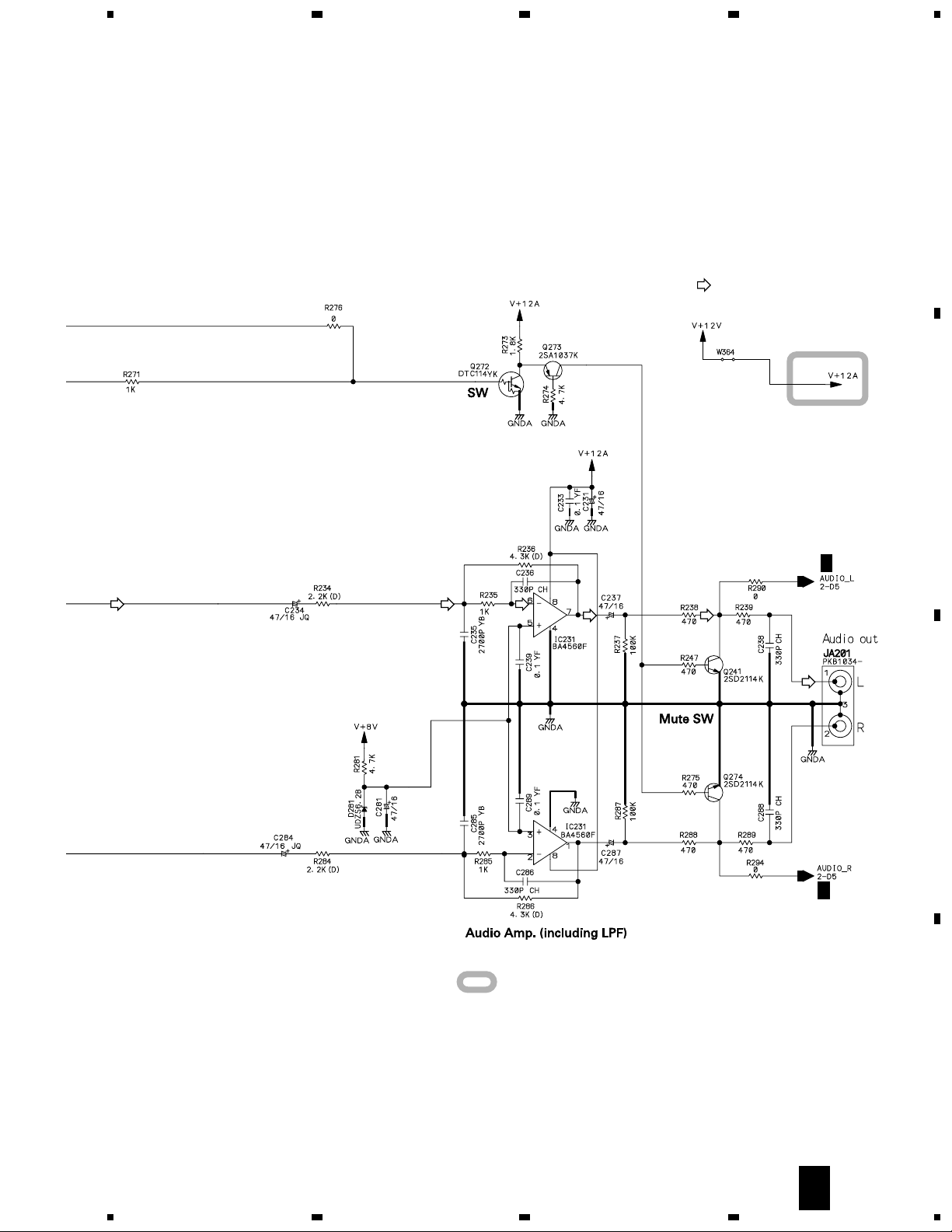
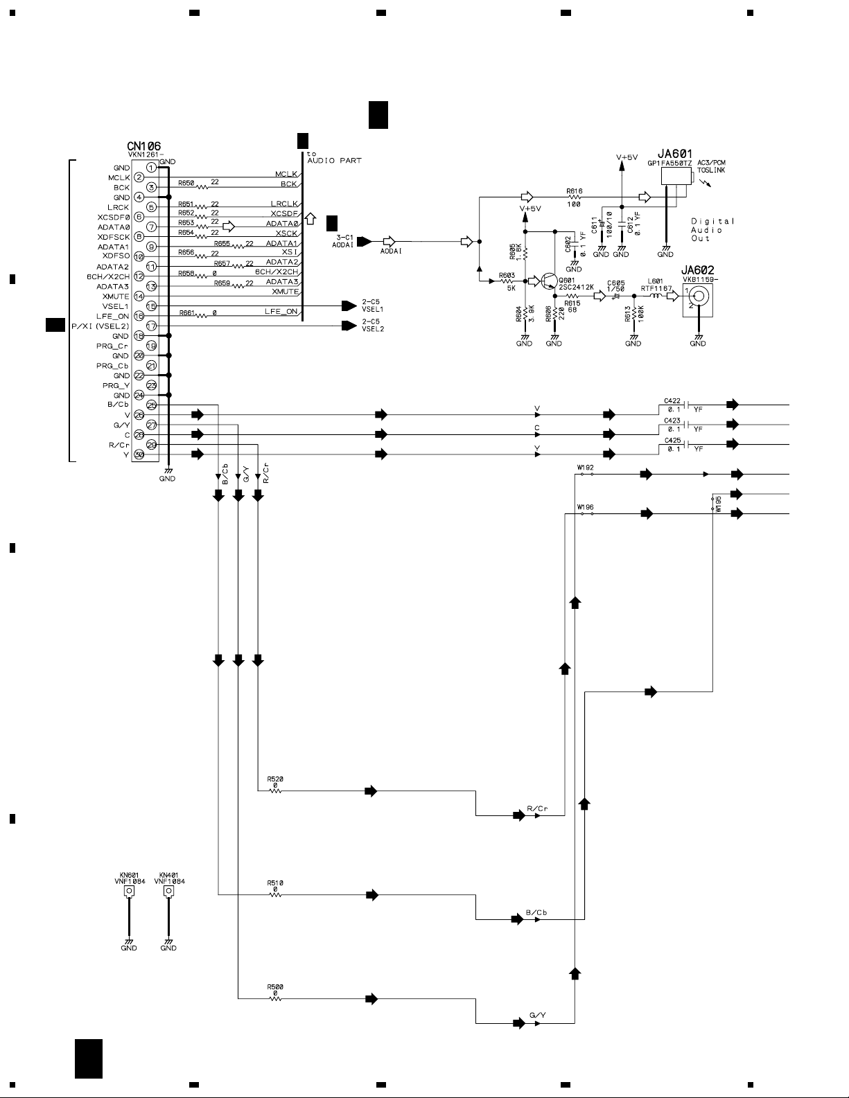
3.7 JACB ASSY (1/3)
A
23
4
D 1/3
JACB ASSY
(DV-545 : VWV1843)
(DV-444-S, K : VWV1842)
CONTROL
INPUT
CN101
G
B
CN101
F
C
CN31
B 2/4
(D)
D
22
1/3
D
1234
D
3/3
D
3/3
D
3/3
(D)
: AUDIO (DIGITAL) SIGNAL ROUTE
: The power supply is shown with the marked box.
Page 23

DV-545, DV-444-S, DV-444-K
23
Page 24
1
DV-545, DV-444-S, DV-444-K
3.8 JACB ASSY (2/3)
A
23
4
D 2/3
D
3/3
JACB ASSY
(DV-545 : VWV1843)
(DV-444-S, K : VWV1842)
B
3
1
4
2
5
C
D
24
2/3
D
1234
Page 25
5
678
DV-545, DV-444-S, DV-444-K
A
: AUDIO SIGNAL ROUTE
B
D
D
: The power supply is shown with the marked box.
3/3
C
3/3
D
2/3
D
5
6
7
8
25
Page 26
1
23
DV-545, DV-444-S, DV-444-K
4
3.9 JACB ASSY (3/3)
A
CN32
B 4/4
B
(V)
(C)
(Y)
D 3/3
D
2/3
D
1/3
(D) (D)
(V)
(C)
(Y)
(B)
(R)
(G)
JACB ASSY
(DV-545 : VWV1843)
(DV-444-S, K : VWV1842)
(D)
(D)
(D) (D)
(V)
(C)
(Y)
(D)
(G)
(V)
(C)
(Y)
(G)
(B)
(R)(R)
(G)(G)
(B)
(R)
(G)
C
(R)
(R)
(B)
(B)
D
(G)
(G)
(R)
(B)
(B)
26
3/3
D
1234
Page 27
5
D
1/3
D
1/3
(V)
(C)
(Y)
(G)
(B) (B)
(R)
(C)
(Y)
(V)
678
DV-545, DV-444-S, DV-444-K
: The power supply is shown with the marked box.
(R)
(V)
(C)
(G)
D432
1SS355
7
8
(Y)
D431
1SS355
(V)
(Y)
(C)
(V)
(Y)
V+8V
(V)
1SS355
1SS355
(Y)
D435
1SS355
(C) (C)
(C)
(D)
(V)
D441
D442
6
D436
1SS355
8
10
9
: V SIGNAL ROUTE
: Y SIGNAL ROUTE
: C SIGNAL ROUTE
(Y)
(C)
(Y)
(R)
(V)
S TERMINAL
OUTPUT
: R SIGNAL ROUTE
(G)
: G SIGNAL ROUTE
(B)
: B SIGNAL ROUTE
: AUDIO SIGNAL ROUTE: AUDIO (DIGITAL) SIGNAL ROUTE
COMPOSITE
VIDEO
OUTPUT
A
B
(G)
(B)
(R)
C
(C)(C)
(Y)(Y)
(V)(V)
(G)
(B)
(R)
(G)
(B)
(R)
E
CN701
D
D
2/3
D
2/3
D
1/3
3/3
D
5
6
7
8
27
Page 28
1
DV-545, DV-444-S, DV-444-K
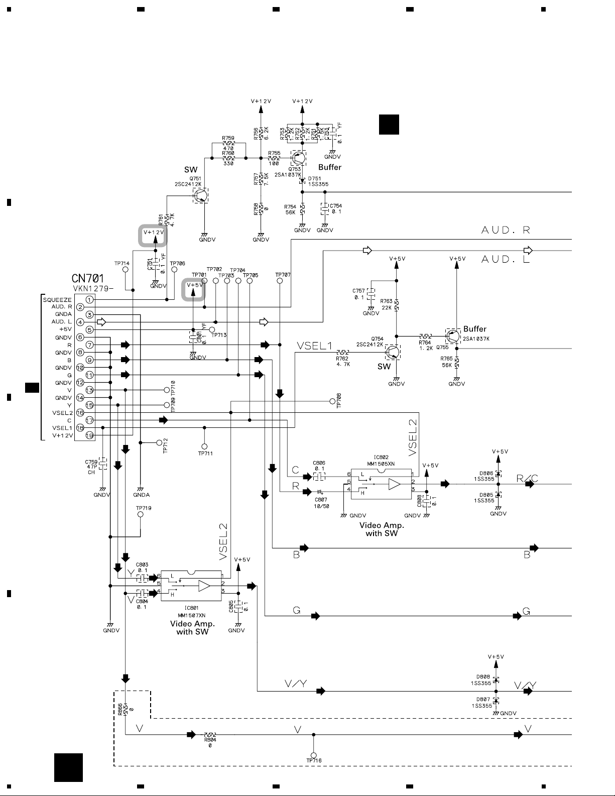
3.10 SRCB ASSY
A
B
23
E
SRCB ASSY
(DV-545 : VWV1848)
(DV-444-S, K : VWV1847)
4
(R)
(B)
CN405
(G)
D 3/3
(C)
(V)
(Y)(Y)
C
(V)
(Y)
(V)
(V/Y)
(B)
(G)
(R)
(G)
(R)
(B)
(C)
(R)
(B)
(G)
(R/C)
(R/C)
(B)
(G)
(V)
D
28
E
1234
DV-545
ONLY
(V)
(V/Y)
(V/Y)
(V)
Page 29
5
678
DV-545, DV-444-S, DV-444-K
: The power supply is shown with the marked box.
DV-545
ONLY
1SS355
DV-444-S, K
ONLY
DV-545
ONLY
DV-444-S, K
ONLY
DV-444-S, K
ONLY
(V)
: V SIGNAL ROUTE
(Y)
: Y SIGNAL ROUTE
(C)
: C SIGNAL ROUTE
(R/C)
DV-545
ONLY
(V/Y)
(G)
(B)
(R)
: R SIGNAL ROUTE
(G)
: G SIGNAL ROUTE
(B)
: B SIGNAL ROUTE
: AUDIO SIGNAL ROUTE
(R/C)
A
B
DV-545
ONLY
(R/C) (R/C)
(B) (B)
(G)
DV-444-S, K
ONLY
(V/Y)
(V/Y)
DV-545
ONLY
(V)
(G)
DV-444-S, K
ONLY
(V)
(V)
DV-444-S, K
ONLY
(B)
(G)
(V/Y)
(R/C)
DV-545
ONLY
(V/Y)
(V)
(V/Y)
DV-545
ONLY
(B) (B)
(V/Y)
(G)
DV-545
ONLY
(V)
C
(V)
DV-545
ONLY
(V)
D
E
5
6
7
8
29
Page 30
1
23
DV-545, DV-444-S, DV-444-K
3.11 FLKB and KEYB ASSYS
4
A
FLKB ASSY (DV-545 : VWG2283)
F
(DV-444-S, K : VWG2282)
DV-545
ONLY
DV-545
ONLY
B
DV-444-S, K
ONLY
DV-545
ONLY
DV-444-S, K
ONLY
DV-545
ONLY
C
D
30
F
1234
Page 31

5
678
DV-545, DV-444-S, DV-444-K
G
Remote Control
IR Signal
Receiver Unit
KEYB ASSY (DV-545 : VWG2291)
(DV-444-S, K : VWG2290)
DV-545
ONLY
: The power supply is shown with the marked box.
FLKB ASSY
S101 : 8 (PAUSE)
S102 : 7 (STOP)
S203 : 3 (PLAY)
KEYB ASSY
S103 : ¡ ¢ (FWD)
S104 : 4 1 (REV)
S105 : Legato PRO (DV-545 ONLY)
S201 : 3 (PLAY)
S202 : (STANDBY/ON)
A
B
C
D 1/3
CN104
D
GF
5
6
7
8
31
Page 32

1
CN1
CN101
AC IN
A
A
B
B
6
8
4
2
1
10
11
14
12
13
12V
6V
EV5V
SW5V
PO CONT
SW3.3V
GND
–27V
FLAC (B)
FLAC (A)
GND
3
GND
5
GND
7
GND
9
CN101
D 1/3
F101
REK1102
2.5A
Z1
C1
LIVE
NEUTRAL
C2
C5
C5
C82
C8
C7
GND
BEA1
BEA2
R2
R71
R72
Q71
D71
R74 R73
D72
D7
D23
D24
C22
C11
C108
R301
R304
C302
R302
R307
R104
R403
R404
R405
Q401
Q402
D402 D403
R401
R420
R303
R410
Q412
R402
C110
R414
R407
R408
R409
D404
R103
R10
C9
R8
C21
C10
D25
R20
R12
D5
R17
D9
R23
R201
R202
R205
R203
R204
VR201
C201
R24
R25
R11
R22
D8
D4
PC1
D6
R9
Q20
Q1
Q2
PC2
PC1
IC201
R7
R6
R5
R19
R1
D14
D13
T1
D11
D12
D81
D82
D83
R84 R85
Q81
R82R83
C81
L1
D105
D104
C107
D103
D102
P101
AEK7063
P102
AEK7066
C105
C106
C410
L101
C109
Q411
Q410
D111
D407
D112
D405
D406
D107
D301
D108
D109
D304
C112
PC2
C111
C411
IC103
IC102
C301
C303
800mA
1.6A
NOTE OF SPARE PARTS IN POWER SUPPLY (SYPS) UNIT
• In case of repairing, use the described parts only to prevent an accident.
• Please write the red mark on the board when the primary section of POWER SUPPLY (SYPS) Unit is repaired.
• Please take care to keep the space, not touching other parts when replacing the parts.
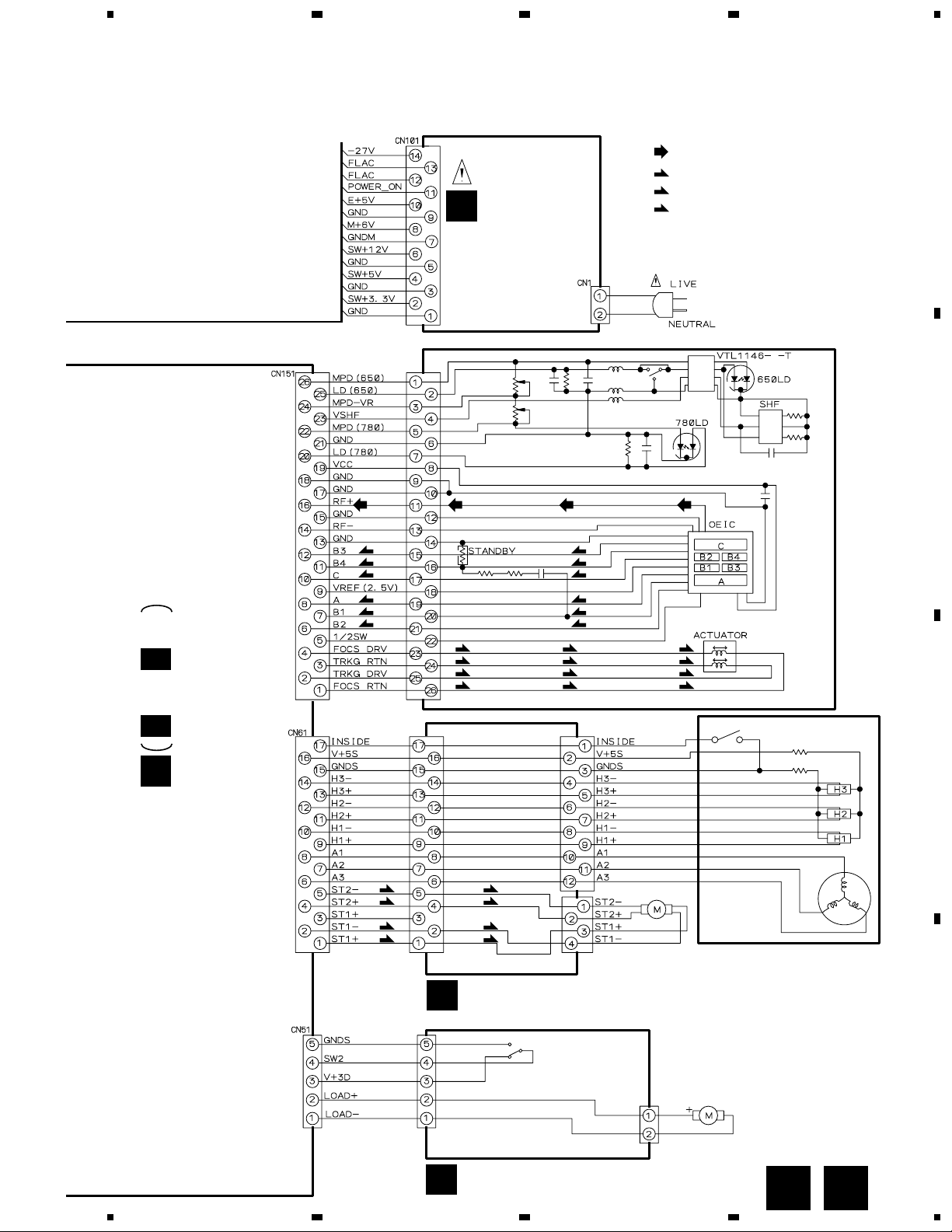
POWER SUPPLY UNIT (VWR1340)
H
BEA401
BEA3
DV-545, DV-444-S, DV-444-K
3.12 POWER SUPPLY UNIT
A
23
4
B
C
D
32
H
1234
Page 33

WAVEFORMS
Note : The encircled numbers denote measuring point in the schematic diagram.
DV-545, DV-444-S, DV-444-K
DVDM ASSY
B
Measurement condition : No. 1 to 4 and 6 to 11 : MJK1, Title 1-chp 1
No. 5 : CD, ABEX-784 Track 1
Foot of R104 (RF)
1
V: 100mV/div. H: 0.2µsec/div.
TP117 (RFO)
2
V: 500mV/div. H: 0.1µsec/div.
3
GND
GND
TP209 (FG)
7
V: 1V/div. H: 5msec/div.
Foot of R261 (FPWM)
8
V: 1V/div. H: 5msec/div.
Foot of R262 (VPWM)
9
V: 1V/div. H: 5msec/div.
JACB ASSY
D
Measurement condition : No. 1 to 5 : DVD-REF-A1, T1-Chap.1
No. 6 to 10 : DVD-REF-A1, T1-Chap.19
IC211 - pin 2 (ADATA)
1
V: 1V/div. H: 500nsec/div.
IC211 - pin 7, 8 (AUDIO L, R)
2
V: 1V/div. H: 50µsec/div.
IC211 - pin 1 (BCK)
3
V: 1V/div. H: 100nsec/div.
IC411 - pin 27 (V)
7
V: 1V/div. H: 10µsec/div.
IC411 - pin 20, 23 (G)
8
V: 1V/div. H: 10µsec/div.
IC411 - pin 18 (B)
9
V: 1V/div. H: 10µsec/div.
TP122 (Tracking Error)
4
(AI-Inner Tracking Off)
V: 500mV/div. H: 2msec/div.
IC201 - pin 39 (EFM before slice)
5
V: 1V/div. H: 1µsec/div.
IC201 - pin 1 (EFM)
6
V: 1V/div. H: 0.2µsec/div.
GND
GND
Foot of R263 (PPWM)
10
V: 1V/div. H: 5msec/div.
Foot of R264 (RPWM)
11
V: 1V/div. H: 5msec/div.
IC211 - pin 3 (LRCK)
4
V: 1V/div. H: 5µsec/div.
IC211 - pin 16 (MCK)
5
V: 1V/div. H: 20nsec/div.
IC411 - pin 25 (C)
6
V: 1V/div. H: 10µsec/div.
IC411 - pin 16 (R)
10
V: 1V/div. H: 10µsec/div.
33
Page 34

DV-545, DV-444-S, DV-444-K
34
Page 35

1
SIDE A SIDE B
4.1 LOAB and SSIB ASSYS
(VNP1836-B)
(VNP1820-B)
(VNP1820-B)
(VNP1836-B)
CN51
B
LOAB ASSY
A
SSIB ASSY
C
SSIB ASSY
C
LOAB ASSY
A
CN61
B
LOADING
MOTOR
ASSY
M
SPINDLE
MOTOR
M
STEPPING
MOTOR
(CARRIAGE)
M
NOTE FOR PCB DIAGRAMS :
1. Part numbers in PCB diagrams match those in the schematic
diagrams.
2. A comparison between the main parts of PCB and schematic
diagrams is shown below.
3. The parts mounted on this PCB include all necessary parts for
several destinations.
For further information for respective destinations, be sure to
check with the schematic diagram.
4. View point of PCB diagrams.
Symbol In PCB
Diagrams
Symbol In Schematic
Diagrams
Part Name
BCE
D
DGGSS
BCE
BCE
DGS
BCEBCE
BCE
Transistor
Transistor
with resistor
Field effect
transistor
Resistor array
3-terminal
regulator
Capacitor
Connector
P.C.Board
Chip Part
SIDE A
SIDE B
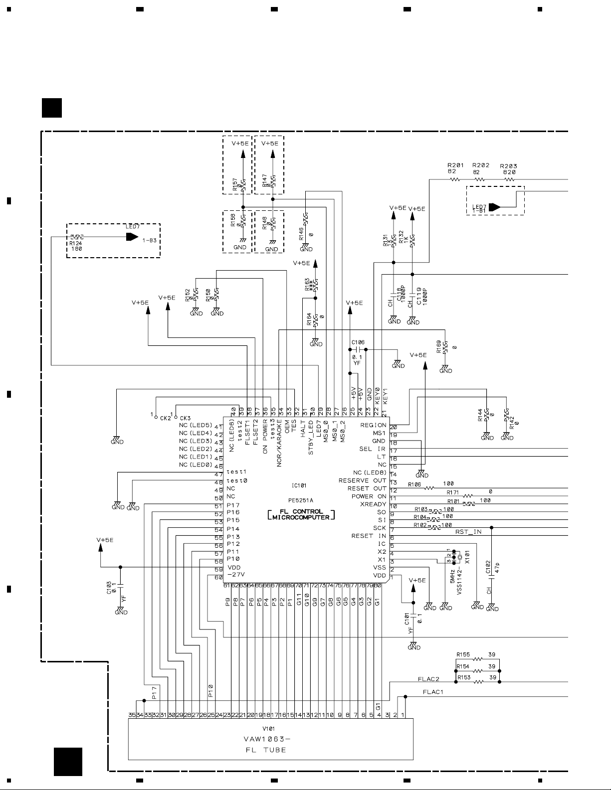
4. PCB CONNECTION DIAGRAM
234
DV-545, DV-444-S, DV-444-K
A
B
C
1
2
D
CA
3
4
35
Page 36

1
23
DV-545, DV-444-S, DV-444-K
4.2 DVDM ASSY
4
CN102
A
B
DVDM ASSY
B
D
PICKUP ASSY
Q601
IC608
IC612
IC601
IC712
Q141
IC481
Q111
IC451
Q115
IC281
Q571
Q107
Q114
IC302
IC261
Q117
Q108
Q118
Q116
IC304
IC303
Q109
C
(DV-545 : VNP1822-A)
(DV-444-S, DV-444-K : VNP1823-A)
D
CN106
D
SIDE A
A
CN601
C
IC805 IC806
IC861
IC881
Q911 Q913 Q902
Q922
Q923
CN3
Q102
IC201
IC351
36
B
1234
Page 37

SIDE B
DVDM ASSY
B
IC603
IC701
IC299
Q542
Q543
Q106
Q103
Q271
Q171
Q281
Q112
Q130
Q241
Q292
Q901 Q903 Q912
Q921
IC101
IC271
IC291
IC111
IC251
IC807
Q142
IC801
(DV-545 : VNP1822-A)
(DV-444-S, DV-444-K : VNP1823-A)
1
234
DV-545, DV-444-S, DV-444-K
A
B
C
D
B
1
2
3
4
37
Page 38

1
23
DV-545, DV-444-S, DV-444-K
4.3 JACB ASSY
4
A
JACB ASSY
D
F
CN101
B
CN31
B
C
B
CN32
E
CN701
D
38
IC571
D
1234
IC411
IC401
IC301
IC211
IC302IC311
IC331IC325
Page 39

5
678
DV-545, DV-444-S, DV-444-K
SY
A
SIDE A
B
(VNP1820-B)
H
CN101
C
D
IC201IC371IC351IC231IC331 Q291
D
5
6
7
8
39
Page 40

1
A
3
23
DV-545, DV-444-S, DV-444-K
4
A
D
J
SIDE B
B
(VNP1820-B)
C
D
40
IC602
IC371
Q399
IC351Q301-Q303Q601
Q334-Q337Q391-Q397
IC231
Q241
D
1234
Q272-Q274
Q351
Q331 Q251
IC331
Q
I
Page 41

5
678
DV-545, DV-444-S, DV-444-K
JACB ASSY
D
A
B
4
Q331 Q251
Q351
IC331
Q352
IC325
C
D
Q276 Q211 IC211
Q261-Q264
5
IC301
6
IC311
IC221 Q314
IC180
Q541 Q531Q321
Q501 Q511
Q521
Q551
IC571
7
Q445-Q448
Q571Q572IC411
D
8
41
Page 42

1
23
DV-545, DV-444-S, DV-444-K
4.4 SRCB ASSY
4
A
SRCB ASSY
E
B
Q801 Q802
CN405
D
(VNP1820-B)
SIDE A
SRCB ASSY
E
C
D
(VNP1820-B)
Q754 Q755 IC802 IC801 Q752
Q753
Q751
42
SIDE B
E
1234
Page 43

1
4.5 FLKB ASSY
234
DV-545, DV-444-S, DV-444-K
FLKB ASSY
F
D
CN104
FLKB ASSY
F
A
IC102
B
IC101
(DV-545 : VNP1832-A)
(DV-444-S, DV-444-K : VNP1833-A)
SIDE A SIDE B
1
C
(DV-545 : VNP1832-A)
(DV-444-S, DV-444-K : VNP1833-A)
D
G
CN201
F
2
3
4
43
Page 44

1
23
DV-545, DV-444-S, DV-444-K
4.6 KEYB ASSY
4
A
B
KEYB ASSY
G
KEYB ASSY
G
C
D
(DV-545 : VNP1834-A)
(DV-444-S, DV-444-K : VNP1835-A)
F
SIDE A SIDE B
44
CN102
G
1234
Page 45

1
4.7 POWER SUPPLY UNIT
234
DV-545, DV-444-S, DV-444-K
AC IN
POWER SUPPLY UNIT
H
Q71Q2
Q1
A
B
Q401
Q402
Q412
Q20
IC201
IC103
IC102
Q410
Q411
VR
201
C
D
CN101
D
SIDE A
H
1
2
3
4
45
Page 46

DV-545, DV444-S, DV-444-K
Mark No. Description Part No. Mark No. Description Part No.
5. PCB PARTS LIST
NOTES:•Parts marked by "NSP" are generally unavailable because they are not in our Master Spare Parts List.
Mark Symbol and Description
NSP
NSP
The mark found on some component parts indicates the importance of the safety factor of the part.
•
Therefore, when replacing, be sure to use parts of identical designation.
When ordering resistors, first convert resistance values into code form as shown in the following examples.
•
Ex.1 When there are 2 effective digits (any digit apart from 0), such as 560 ohm and 47k ohm (tolerance is shown by J=5%,
and K=10%).
560 Ω→56 × 10
47k Ω→47 × 10
0.5 Ω→R50 ..................................................................................... RN2H
1 Ω→1R0 ..................................................................................... RS1P
Ex.2 When there are 3 effective digits (such as in high precision metal film resistors).
5.62k Ω→ 562 × 10
1
→ 561 ........................................................ RD1/4PU 5 6 1 J
3
→ 473 ........................................................ RD1/4PU 4 7 3 J
R 5 0
1 R 0
1
→ 5621 ...................................................... RN1/4PC 5 6 2 1 F
K
K
LIST OF HOLE PCB ASSEMBLIES
Part No.
DV-545 DV-444-S DV-444-K
WYXQ,
WYXQ/FRGR,
WVXQ
Loading Mechanism Assy
LOAB Assy
WYXJ,
WVXJ
VWT1188
VWG2279
WYXQ,
WYXQ/FRGR,
WVXQ
VWT1188
VWG2279
Remarks
DVDM Assy
NSP
JSMB Assy
SSIB Assy
JACB Assy
SRCB Assy
NSP
FLKB Assy
NSP
KEYB Assy
POWER SUPPLY Unit
JACB ASSY
D
VWS1488
VWM2084
VWG2292
VWV1843
VWV1848
VWG2283
VWG2291
VWR1340
VWS1487
VWM2083
VWG2292
VWV1842
VWV1847
VWG2282
VWG2290
VWR1340
Although VWV1843 and VWV1842 are different in part number, they consist of the same components.
SRCB ASSY
E
VWV1848 and VWV1847 are constructed the same except for the following :
Mark Symbol and Description
D701
C701, C702, C816-C818
C704, C706
C815
RY701, RY702, RY801-RY803
VWV1848 VWV1847
1SS355
CKSRYF104Z25
CCSRCH391J50
CEAT471M6R3
VSR1016
Part No.
Not used
Not used
Not used
Not used
Not used
Remarks
46
R701, R703
R705, R707, R711, R712, R804, R829, R864
R866
R821
R851-R853, R862, R865, R867, R869
JA702 RGB Connector
RS1/16S471J
RS1/16S0R0J
RS1/16S0R0J
RS1/16S75R0F
Not used
VKB1157
Not used
Not used
Not used
Not used
RS1/16S0R0J
Not used
Page 47

DV-545, DV444-S, DV-444-K
Mark No. Description Part No. Mark No. Description Part No.
DVDM ASSY
B
VWS1488 and VWS1487 are constructed the same except for the following :
Mark Symbol and Description
IC271
IC281
IC303
IC304
IC712
VWS1488 VWS1487
TC74HC4053AFT
BA4510F
TC7SZU04F
TC7SZU04F
MSM51V17805D-60TS
Part No.
Remarks
Not used
Not used
Not used
TC7SHU04F
MNR4800DJ7
IC807
Q271, Q281
D303
C271-C274
C275
C279, C285, C828, C830
C281, C282
C283, C284, C899
C286
C314
C322
C324
C329
C741
R3, R622
R4
R215, R273, R321, R712, R763, R765, R767
R771, R825-R827
R274, R279
R275, R281-R284, R290
R285, R286
R287
R288
R289
R310
R312
R314
R328
R329
R332
PD0274A
DTC114EUA
KV1470
CKSRYB223K50
CKSRYB102K50
CKSRYF104Z25
CCSRCH5R0C50
CCSRCH470J50
CCSRCH680J50
CCSRCH150J50
CKSRYB103K50
CCSRCH331J50
CKSRYF105Z10
CEV221M4
Not used
RS1/16S103J
Not used
Not used
RS1/16S473J
RS1/16S472J
RS1/16S683J
RS1/16S1002F
RS1/16S2201F
RS1/16S1503F
RS1/16S823J
RS1/16S103J
RS1/16S223J
RS1/16S102J
RS1/16S332J
RS1/16S471J
Not used
Not used
Not used
Not used
Not used
Not used
Not used
Not used
Not used
CCSRCH220J50
CCSRCH180J50
Not used
Not used
CEV101M16
RS1/16S103J
RS1/16S333J
RS1/16S0R0J
RS1/16S0R0J
Not used
Not used
Not used
Not used
Not used
Not used
RS1/16S473J
RS1/16S153J
RS1/16S103J
RS1/16S182J
RS1/16S222J
RS1/16S331J
R335
R336
R713, R761, R764, R766, R768, R772
R822, R823, R824
NSP
PC Board DVDM
FLKB ASSY
F
RS1/16S682J
RS1/16S104J
RS1/16S0R0J
RS1/16S220J
VNP1822
VWG2283 and VWG2282 are constructed the same except for the following :
Mark Symbol and Description
R124
R147, R158
R148, R157
PC Board FLKB
VWG2283 VWG2282
RS1/16S181J
Not used
RS1/16S0R0J
VNP1832
Part No.
Not used
RS1/16S0R0J
Not used
Not used
VNP1823
Remarks
Not used
RS1/16S0R0J
Not used
VNP1833
47
Page 48

DV-545, DV444-S, DV-444-K
Mark No. Description Part No. Mark No. Description Part No.
KEYB ASSY
G
VWG2291 and VWG2290 are constructed the same except for the following :
Mark Symbol and Description
D202
S105
R184
PC Board KEYB
VWG2291 VWG2290
SLR-343DC
ASG7013
RS1/16S151J
VNP1834
PCB PARTS LIST FOR DV-545/WYXJ UNLESS OTHERWISE NOTED
Part No.
Remarks
Not used
Not used
Not used
VNP1835
Mark No. Description Part No.
LOAB ASSY
A
SWITCH
S101 VSK1011
OTHERS
CN602 KR CONNECTOR S2B-PH-K
CN601 KR CONNECTOR S5B-PH-K
DVDM ASSY
B
PC BOARD LOAB VNP1836
SEMICONDUCTORS
IC451 BA25BC0FP
IC861 ADV7172KST
IC261,IC281,IC302 BA4510F
IC251 BA6664FM
IC481 BU2288FV
IC101 LA9701M
IC201 LC78652W
IC351 M56788AFP
IC801 M65774BFP
IC805 MB81F161622C-80FN
IC712 MSM51V17805D-60TS
IC807 PD0274A-TFB
IC601 PD6345A
IC701 PE5108A
IC111,IC271 TC74HC4053AFT
IC612 TC74VHC125FT
IC608 TC74VHCT125AFT
IC303,IC304 TC7SZU04F
IC603 VYW1852
Q109,Q901-Q903,Q911-Q913 2SA1576A
Q114,Q130 2SC4081
Q107,Q111,Q115,Q241,Q271 DTC114EUA
Q281 DTC114EUA
Q101,Q102,Q106 HN1A01F
Q103,Q141,Q142,Q542,Q543 HN1B04FU
Q112,Q113 HN1C01FU
Q108 HN1K03FU
Q571 RN1911
Q117,Q171,Q601 RN4982
D302,D303 KV1470
D601 RB501V-40
Mark No. Description Part No.
COILS
L304 LCYA1R5J2520
L481 CHIP BEAD VTL1084
L489 CHIP BEAD VTL1078
CAPACITORS
C480,C481,C612 CCSRCH100D50
C152 CCSRCH101J50
C104-C108,C314 CCSRCH150J50
C151 CCSRCH270J50
C324,C391,C392 CCSRCH331J50
C146 CCSRCH390J50
C122,C123 CCSRCH391J50
C116,C134,C283,C284,C297 CCSRCH470J50
C899 CCSRCH470J50
C145,C241 CCSRCH560J50
C281,C282 CCSRCH5R0C50
C286 CCSRCH680J50
C117,C360 CCSRCH681J50
C124 CCSRCH820J50
C129,C149,C201,C205,C254 CEV101M16
C358,C368,C369,C401,C403,C410 CEV101M16
C407,C472,C864 CEV101M16
C113,C139 CEV220M16
C142,C405,C454,C715,C741 CEV221M4
C111 CEV470M6R3
C140,C223,C224,C264,C312 CKSQYB105K10
C475-C477 CKSQYB105K10
C209,C211,C216,C275,C313 CKSRYB102K50
C351 CKSRYB102K50
C133,C136,C203,C220,C225 CKSRYB103K50
C239,C261,C320-C322,C330 CKSRYB103K50
C591,C619,C703,C722 CKSRYB103K50
C101,C103,C118,C119,C121 CKSRYB104K16
C212,C213,C227,C231 CKSRYB104K16
C248-C251,C255,C263,C315 CKSRYB104K16
C317 CKSRYB104K16
C208,C210 CKSRYB222K50
C271-C274 CKSRYB223K50
C266 CKSRYB224K10
C206,C214,C242,C357 CKSRYB472K50
C102,C109,C120,C130,C131 CKSRYF104Z25
C138,C143,C148,C154 CKSRYF104Z25
C157,C158,C204,C207,C215 CKSRYF104Z25
C221,C222,C226,C230,C236 CKSRYF104Z25
C253,C256,C258,C265,C279 CKSRYF104Z25
48
Page 49

DV-545, DV444-S, DV-444-K
Mark No. Description Part No. Mark No. Description Part No.
C285,C299,C319,C332,C353 CKSRYF104Z25
C359,C365,C366,C453,C603 CKSRYF104Z25
C606,C608-C611,C613,C615 CKSRYF104Z25
C618,C626,C628,C631,C704 CKSRYF104Z25
C706,C708,C712,C713 CKSRYF104Z25
C716-C718,C721,C723,C725 CKSRYF104Z25
C743,C802,C808,C811,C814 CKSRYF104Z25
C828,C830,C866,C869-C872 CKSRYF104Z25
C874,C875,C903,C913 CKSRYF104Z25
C115,C217,C328,C329,C607,C614 CKSRYF105Z10
C710,C711,C714,C726,C801,C809 CKSRYF105Z10
C813,C816-C821,C827,C833,C843 CKSRYF105Z10
RESISTORS
R815,R819 RAB4C0R0J
R543,R545,R594,R631,R707 RAB4C103J
R121 RAB4C220J
R123 RAB4C470J
R400,R403 RS1/10S0R0J
R341 RS1/10S101J
R126-R129,R176-R179 RS1/10S220J
R902,R905,R908,R912,R915 RS1/16S1000F
R918 RS1/16S1000F
R287 RS1/16S1002F
R364,R369,R373,R375 RS1/16S1003F
R865 RS1/16S1502F
R289,R358,R361 RS1/16S1503F
R288 RS1/16S2201F
R876,R878 RS1/16S4701F
R866 RS1/16S4702F
R870,R875 RS1/16S6800F
R867 RS1/16S6801F
R357,R362,R363,R368,R372 RS1/16S6802F
R374 RS1/16S6802F
R257 (1Ω) VCN1127
R258,R259 (2.2Ω) VCN1128
Other Resistors RS1/16S J
OTHERS
CN51 PH CONNECTOR S5B-PH-SM3
9007 FLEXIBLE CABLE (07P) VDA1681
CN61 17P FFC CONNECTOR VKN1421
CN31,CN32 30P FFC CONNECTOR VKN1434
CN151 26P FFC CONNECTOR VKN1790
X481 CRYSTAL RESONATOR VSS1159
X601 CERAMIC RESONATOR VSS1160
SSIB ASSY
C
(27.000MHz)
(16.5MHz)
OTHERS
CN2 4P FFC CONNECTOR VKN1264
CN1 12P FFC CONNECTOR VKN1272
CN3 17P FFC CONNECTOR VKN1277
JACB ASSY
D
SEMICONDUCTORS
IC231 BA4560F
IC302 NJM78L05A
IC411 MM1540BF
IC401 NJM78L08A
IC211 PCM1742KE
Q273 2SA1037K
Q601 2SC2412K
Q241,Q274 2SD2114K
Q211,Q272,Q445,Q447 DTC114YK
Q446,Q448 PDTA124EK
D150,D431,D432,D435,D436 1SS355
D441,D442,D471,D472 1SS355
D475,D476,D481,D482 1SS355
D281 UDZS6.2B
COIL
L601 NOISE FILTER RTF1167
CAPACITORS
C236,C238,C286,C288 CCSRCH331J50
C150 CCSRCH470J50
C411 CEAL101M10
C415 CEAL470M10
C405,C611 CEAT101M10
C605 CEAT1R0M50
C231,C237,C281,C287 CEAT470M16
C105 CEAT471M16
C431,C441 CEAT471M6R3
C213,C215 CEJQ101M6R3
C206,C211 CEJQ331M6R3
C234,C284 CEJQ470M16
C235,C285 CKSRYB272K50
C106,C151,C212,C214,C216 CKSRYF104Z25
C233,C239,C289,C406,C412 CKSRYF104Z25
C416,C422,C423,C425,C435 CKSRYF104Z25
C582,C584,C586,C602,C612 CKSRYF104Z25
RESISTORS
R234,R284 RN1/16SE2201D
R236,R286 RN1/16SE4301D
R273 RS1/10S182J
R432,R436,R442 RS1/16S75R0F
Other Resistors RS1/16S J
OTHERS
CN101 FJ CONNECTOR 14P 14PL-FJ
CN401 4P MINI DIN SOCKET AKP7008
JA601 OPTICAL LINK OUT GP1FA550TZ
JA201 2P PIN JACK PKB1034
JA150 REMOTE CONTROL JACK RKN1004
9001 PCB BINDER VEF1040
JA402 1P PIN JACK VKB1122
JA602 1P PIN JACK (BLK, NI) VKB1159
CN104 16P FFC CONNECTOR VKN1247
CN405 19P FFC CONNECTOR VKN1250
CN102,CN106 VKN1261
30P FFC CONNECTOR
CN110 7P FFC CONNECTOR VKN1267
KN401,KN601 VNF1084
EARTH METAL FITTING
49
Page 50

DV-545, DV444-S, DV-444-K
Mark No. Description Part No. Mark No. Description Part No.
SRCB ASSY
E
SEMICONDUCTORS
IC802 MM1505XN
IC801 MM1507XN
Q753,Q755 2SA1037K
Q751,Q754 2SC2412K
D701,D751,D805-D808 1SS355
RELAYS
RY701,RY702,RY801-RY803 VSR1016
CAPACITORS
C703-C706 CCSRCH391J50
C759 CCSRCH470J50
C807 CEAT100M50
C811-C813 CEAT101M10
C814,C815 CEAT471M6R3
C701,C702,C751,C753,C754 CKSRYF104Z25
C757,C758,C801,C803-C806 CKSRYF104Z25
C808,C816-C818,C894 CKSRYF104Z25
RESISTORS
R766 RS1/16S68R0F
R809,R813,R817,R820,R821 RS1/16S75R0F
Other Resistors RS1/16S J
OTHERS
JA701,JA702 RGB CONNECTOR VKB1157
CN701 19P FFC CONNECTOR VKN1279
KEYB ASSY
F
SEMICONDUCTOR
D202 SLR-343DC(NPQ)
SWITCHES
S103-S105,S201,S202 ASG7013
RESISTORS
All Resistors RS1/16S J
OTHERS
CN201 FJ CONNECTOR 4P 04R-FJ
POWER SUPPLY UNIT
G
PC BOARD KEYB VNP1834
OTHERS
P101 PROTECTOR (800mA) AEK7063
P102 PROTECTOR (1.6A) AEK7066
F1 FUSE (2.5A) REK1102
FLKB ASSY
F
SEMICONDUCTORS
IC101 PE5251A
IC102 PST3242
SWITCHES
S101,S102,S203 ASG7013
CAPACITORS
C111,C114,C118,C119 CCSRCH102J50
C102 CCSRCH470J50
C122 CEAL101M6R3
C101,C103,C106,C112,C121 CKSRYF104Z25
C131 CKSRYF104Z25
C105 CKSRYF104Z50
RESISTORS
All Resistors RS1/16S J
OTHERS
CN102 FJ CONNECTOR 4P 04P-FJ
IR101 REMOTE RECEIVER UNIT GP1U27X
V101 FL TUBE VAW1063
CN101 16P FFC CONNECTOR VKN1276
X101 CERAMIC RESONATOR VSS1142
SPACER VEC2220
FL HOLDER VNF1122
PC BOARD FLKB VNP1832
(5MHz)
50
Page 51

6. ADJUSTMENT
DV-545, DV-444-S, DV-444-K
6.1 ADJUSTMENT ITEMS AND
LOCATION
Adjustment Items
[Mechanism Part]
1
Tangential and Radial Height Coarse Adjustment
2
DVD Jitter Adjustment
3
Initialize the Focus Sweep Setting
[Electrical Part]
Electrical adjustments are not required.
Adjustment Points (Mechanism Part)
Cautions: After adjustment, adjustment screw locks with the
Screw tight.
6.2 JIGS AND MEASURING
INSTRUMENTS
Screwdriver (large)
TV monitor
Screwdriver (medium)
Test mode remote control
unit (GGF1067)
1 2
Tangential
adjustment
screw
1 2
Radial
adjustment
screw
Precise screwdriver
Screw tight
(GYL1001)
DVD test disc
(GGV1025)
51
Page 52

DV-545, DV-444-S, DV-444-K
6.3 NECESSARY ADJUSTMENT POINTS
When Adjustment Points
Exchange Parts of Mechanism Assy
Exchange the Pickup
Exchange the Traverse Mechanism
Exchange the Spindle Motor
Exchange PCB Assy
Exchange PC Board
Mechanical
point
Electric
point
Mechanical
point
Electric
point
Mechanical
point
Electric
point
Mechanical
point
~, Ÿ, !
!
Ÿ, !
∗ After adjustment, screw locks
with the Screw tight.
∗ After adjustment, screw locks
with the Screw tight.
SSIB, LOAB, DVDM ASSY
∗
Purpose: To set the sweep which was correct with the
individual Traverse mechanism.
Be sure to perform the following step finally when replaced
Pickup, Traverse Mechanism and Spindle Motor.
ESC CLEAR
GGF1067
Test mode
remote control
unit
(It is necessary when performed adjustment procedure Ÿ.)
Electric
point
52
Page 53

TEST MODE: ON
TEST MODE: DISC SET
DSC -
&&&
GGF1067
Test mode
remote control
unit
GGF1067
Test mode
remote control
unit
POWER
ON
<TRAY OPEN>
OPEN/CLOSE
(Player or Remote
Control Unit)
OPEN/CLOSE
(Player or Remote
Control Unit)
DVD disc
TEST MODE: PLAY
TEST MODE: OFF
An address is displayed
For example, when playback with # 30000
During PLAY
Press keys in order
OR
ESC
OFF
POWER
6.4 TEST MODE
030000
<PLAY>
< When playback with the target address of disc (DVD)>
TV/LDP
+10 3 0 0 0 0 CHP/TIM
ESC TEST
CHECK
DVD, CD
DV-545, DV-444-S, DV-444-K
53
Page 54

DV-545, DV-444-S, DV-444-K
6.5 MECHANISM ADJUSTMENT
Tangential and Radial Height Coarse Adjustment
1
START
• Remove the servo mechanism.
• Remove a Spacer for height adjustment
attached to the back side (shaded area)
of the Servo Mechanism (Float Base) with
nippers.
Servo Mechanism
Float Base
Spacer for Height adjustment
Note:
Turn the Short switch to Short side when
removing the Pickup Flexible Cable.
(Refer to "7.1.6 DISASSEMBLY".)
Cautions:
Because there is not a Spacer for height adjustment in
adjustment after the second time, will keep it at need.
(This parts is Traverse mechanism exclusive use of a model
for 2001 years)
7.3mm
Put a spacer between a Tangential (or Radial) adjustment
screw and Mechanism Base and turn each screw to adjust
the height. (Refer to "6.1 ADJUSTMENT ITEMS AND
LOCATION".)
Turn a flat side
into bottom
54
Page 55

DVD Jitter Adjustment
2
DV-545, DV-444-S, DV-444-K
• Playback method of inner and outer address for the purpose is refererd to "6.3 TEST MODE".
• Jitter indication of the monitor is refererd to "7.1.3 TEST MODE SCREEN DISPLAY".
START
• Test mode
• Play the DVD test disc
at outer track
(around #200000)
Mechanism Assy
Adjust the Tangential
Adjustment Screw so that
jitter becomes minimum.
J4 : Min
Use disc: GGV1025
• Play the DVD test disc
at inner track
(around #30000)
Mechanism Assy
Adjust the Radial
Adjustment Screw so that
jitter becomes minimum.
J4 : Min
Turn the POWER OFF in
case of NG once, and
perform the adjustment
once again.
If error rate is OK,
locks a root of
tangential and radial
adjustment screws with
the Screw tight, and
go to step
!
.
CHECK
NG
OK
J4 : - - - -
Player
Monitor
Confirm the error rate that is
displayed "OK"
(Example ER (av): 2.5e - 5-*OK )
Disc playback normally.
• The measurement of block error rate
5ESC
• Play the DVD test disc
at outer track
(around #200000)
Mechanism Assy
Readjust the Tangential
Adjustment Screw so that
jitter becomes minimum.
J4 : Min
ESC
Screw tight : GYL1001
Test mode end
55
Page 56

DV-545, DV-444-S, DV-444-K
Initialize the Focus Sweep Setting
3
Purpose: To set the sweep which was correct with the individual Traverse mechanism.
Turn on the Player
ESC CLEARPOWER
Note: Be sure to perform this step when replaced the Pickup or Traverse mechanism.
56
Page 57

DV-545, DV-444-S, DV-444-K
7. GENERAL INFORMATION
7.1 DIAGNOSIS
7.1.1 SELF-DIAGNOSTIC FUNCTION OF PICKUP DEFECTIVE
This unit can confirm the laser diode current value (DVD: 650nm, CD: 780nm) of pickup on the Test Mode screen.
(Press the ESC → TEST keys in order on the test mode remote control unit (GGF1067) to enter the test mode.)
It's effective in case of the following condition.
Symptom
• Indicates "No Disc" in FL display.
• Player does not playback, etc..
Procedure of Self-Diagnosis
1 Enter the Test mode.
2 When diagnosing the 650nm laser diode:
Press the → keys in order, and turn on the laser diode (It light-up for nine seconds.).
When diagnosing the 780nm laser diode:
Press the → keys in order, and turn on the laser diode (It light-up for nine seconds.).
TEST 1
TEST 4
When let it turn on once again after performed 2 once,
After pressed REP.B key once
650nm: Press the → keys in order
780nm: Press the → keys in order
3 Confirm the indicated value of the laser diode current (LDI). (Refer to following figure.)
4 When indicated value is more than 100, pickup is defective. → Replacement is necessary
Replace the Traverse Mechanism Assy or Pickup.
Note :
When a DVD disc or a CD disc is played in the test mode, this function is effective.
Laser diode current value
TEST 1
TEST 4
Character in bold : Item name
: Information display
Test Mode Screen Display
57
Page 58

DV-545, DV-444-S, DV-444-K
7.1.2 TEST POINTS LOCATION
This model has not test terminal.
Please use following points on the DVDM Assy when checking RF, FE and TE, etc..
DVDM ASSY
CN61
CN151
CN51
RF
(R169)
IC201
CN13
IC351
BCLK
LRCLK
DATAO
for Audio DAC
(IC211)
TE
FE
CN32
Prog. Cr
Color
difference
Cb (/B)
Cr (/R)
Color
Y (/G)
difference
C
V
Y
IC861
IC806 IC805
22M/24M (for DAC)
16M/36M (for AV1)
27M (for AV1)
Prog. Y
Prog. Cb
IC881
Vref
(IC101-pin 64)
RFO
IC712
VCO DRV
CN31
SIDE A
IC481
33M (for BY Chip pin 15)
16M
(for BY Chip pin 13, DSP)
IC601
Front Side
58
Page 59

DV-545, DV-444-S, DV-444-K
7.1.3 TEST MODE SCREEN DISPLAY
TEST MODE SCREEN DISPLAY
When the test mode is entered, press the ESC button and the TEST button in order of the test mode remote control unit (GGF1067).
Consecutive double-OSD display is supported during test mode. The screen is composed 10 lines with a maximum of 32 characters per line.
It can't be used with the debugging display mode together.
• Screen Composition
Address
Background color
Tracking status and
Laser diode current value
Spindle status and AFB status
AGC setting
FTS servo IC information
C1 error value of CD and DVD
Internal operation mode of
the mechanism control
Disc judgment and
CD 1/3 beam switch
Equalizer value and
jitter value
Character in bold : Item name
: Information display
Test Mode Screen Display
(First Screen Display)
Caution :
The first screen and second screen switch by pressing [DISPLAY]
key of the remote control unit.
It is only a version display part on the lower right of the screen
those contents of display change.
ATB : ON/OFF information display and AGC manual setting display
deleted with the second generation.
The displays of Tilt error value, Tilt servo status and pickup
DVD/CLD display deleted with the third generation becomes LD
part is deleted.
Remote control code
Key code
Mechanism position value and
slider position
Output video system and
Skirt terminal output
AV1 chip version
FL controller version and
region setting for the player
FL controller destination setting
Port No. of Flash ROM and
system controller
Flash ROM version and Flash ROM size
System controller revision
DVD mechanism controller revision
(Control and part No. of GUI-ROM)
• Description of Each Item on the Display
(1) Address indication
The address being traced is displayed in number.
DVD : ID indication (hexadecimal number, 8 digits)
[ ∗ ∗ ∗ ∗ ∗ ∗ ∗ ∗ ]
CD : A-TIME (min. sec.) [ 0 0 0 0 ∗ ∗ ∗ ∗ ]
(Note : For DVDs, decimal-number indication is possible.)
(2) Code indication of the remote control unit [R – ∗ ∗ ∗ ∗]
The code for the key pressed on the remote control unit, which
is received by the FL controller, is displayed while the key is
pressed. In the case of the double code, the second code will
be displayed.
(3) Key code indication for the main unit [K – ∗ ∗ ]
The code for the key pressed on the main unit, which is
received by the system controller, is displayed while the key is
pressed.
(4) Background color indication [C – R∗ ∗ G∗ ∗ B∗ ∗]
(5) 1 Tracking status [TRKG – ∗∗∗]
Tracking on [ON ]
Tracking off [OFF]
2 Laser diode current value [LDI – ∗∗∗]
(6) 1 Spindle status [SPDL – ∗ ∗ ∗]
Spindle accelerator and brake, free-runnimg [A/B]
FG servo [FG]
Rough, velocity phase servo [SRV]
Offset addition, rough, velocity phase servo [O_S]
2 AFB status [AFB – ∗ ∗]
ON [ON ]
OFF [OFF]
(7) Mechanism position value [M – ∗]
Position code [1] to [3]
(8) Slider position [S – ∗ ∗ ∗ ∗]
CD TOC area [IN ]
CD active area [CD ]
(9) AGC setting [AGC – ∗ ∗]
AGC on [AGC-ON]
AGC off [AGC-OFF]
59
Page 60

DV-545, DV-444-S, DV-444-K
(10) Output video system [V – ∗ ∗ ∗ ∗]
NTSC system [NTSC]
PAL system [PAL ]
Auto-setting [AUTO]
Skirt terminal output [SK – ∗ ∗]
VIDEO [00]
S-VIDEO [01]
RGB [02]
Note : Display only the model which can do the output setting of
skirt terminal.
(11) FTS servo IC information
DSP coefficient indication [KS – [∗ ∗ ∗ ∗] ∗ ∗ ∗ ∗ ]
Displays the address (four digits) of the specified coefficient
and the setting value (four digits) with [TEST] and [9] keys.
(12) Error rate indication
1 C1 error value of CD [ER – C1 ∗ ∗ ∗ ∗ ]
2 C1 error value of DVD [ER – ∗ ∗ ∗ ∗ ∗ ∗ ∗ ∗ ]
(13) Internal operation mode of mechanism controller
[MM – ∗ ∗ : ∗ ∗]
Internal mechanism mode (2 digits) and internal mechanism
step (2 digits) of the mechanism controller
(14) 1 Disk sensing [DSC – ∗ ∗ ∗]
The type of discs loaded is displayed.
[DVD], [CD ], [VCD], [ ]
2 CD 1/3 beam switch [BM – ∗ ∗]
(20) 1 Version of the flash ROM [V : ∗ . ∗ ∗ ∗]
2 Flash ROM size [FLSH = ∗]
(21) Revision of the system controller [S : ∗ . ∗ ∗ ∗ / ∗ . ∗ ∗ ]
1 Revision number of the external ROM part (flash ROM) of
the system controller <Front>
2 Revision of the internal ROM part of the system controller
<Back>
(22) Revision of the DVD mechanism controller
[M : ∗ . ∗ ∗ ∗]
Revision number of the external ROM part (flash ROM) of the
DVD mechanism controller
(23) Control and part numbers of the GUI-ROM
[GUI : ∗ ∗ ∗ ∗]
No GUI model displays as "––– / ––––".
OEM model displays the part number of GUI-ROM
[GUI : * * * *]
(15) 1 Equalizer value [E – ∗ ∗]
2 Jitter value [J – ∗ ∗]
Make the jitter four times, and renew it in every 0.5
second. [J4 – * *]
CD is effective only in the jitter value.
(16) Version of the AV-1 chip [ AV : ∗ . ∗ ∗' ∗' ]
(17) 1 Version of the FL controller [FL : ∗ ∗ ∗ ∗]
2 Region setting of the player [REG : ∗ ]
Setting value [1] to [6]
(18) Destination setting of the FL controller
[MDL : ∗ ∗ ∗ ∗ / ∗ ∗ ∗ ]
Four charactors in the front represent the type of model :
three charactors in the back represent the destination code.
J : /J, K : /KU, /KC, /KU/KC, R : /RAM, /RL, /RD, /LB,
WY : /WY
(19) The part number of the flash ROM and system
controller [∗ ∗ ∗ ∗ ∗ ∗ / ∗ ∗ ∗ ∗ ∗ ∗ ∗]
1 Part number of the flash ROM <Front>
(Example) VYW1536-A = W1536A
(Example) PD6256A9 = 6256A9
2 Part number of the system controller <Back>
(Example) PD3381T1 = 3381T1
60
Page 61

DV-545, DV-444-S, DV-444-K
DEBUGGING SCREEN SPECIFICATION FOR THE MECHANISM CONTROLLER
• This specifications is subject to change without notice.
1 Indication Method of The Mechanism Controller Debugging Screen
A debugging screen of the mechanism controller is indicated when pressing the test mode remote control unit [GGF1067] in
order of the and buttons.
Releace from debugging screen display of the mechanism controller with the button.
2 Screen Layout
ESC
CHP/TM
ESC
3 Indication Contents
1. The error that became the trigger that an error of 2
occurred.
There are many cases same as 2.
2. The error number that transferred to the system
controller
Refer to the error list about contents of error number.
3. Code read in state (it does not support in this unit)
When X is indicated, ID or subcode are not able to read in.
When X is not indicated, they are able to read in.
4. ID or subcode (it does not support in this unit)
Subcode indicates the A time.
5. Inside mode of the mechanism controller when an error
of 1 occurred
It can indicate to a maximum 10 mode. Indicate it in order of
an old mode from the left, and go right, and become a new
mode. Indicate only a nest share of the mode.
6. Processing step of inside mode of 5
It can grasp the mode reaching an error and transition of step
by watching 5 and 6 and it can specify the occurrence place of
most errors.
7. Disk information in the mechanism controller
? : Indistinctness
NO : There is no disc
DVD 1 : DVD single layer
DVD 2 : DVD dual layer
CD : CD
CDR : CD-R or CD-RW
CDR P : PRD of CD-R or CD-RW
8. As a result of 8cm /12cm distinction
? : Indistinctness (undistinction)
8 : 8 cm
12 : 12 cm
9. OEIC gain (it does not support in this unit)
H : OEIC HIGH gain
L : OEIC LOW gain
10. SGC gain for LD of 780nm
It indicates a step using in the mechanism controller inside
with a hexadecimal number.
Set the gain so that S curve becomes 1.8V (p-p) in disc
distinction.
11. SGC gain for LD of 650nm For L0.
It indicates a step using in the mechanism controller inside
with a hexadecimal number. Set a gain so that S curve
becomes 1.8V (p-p) in disc distinction.
12. SGC gain for LD of 650nm For L1.
It indicates a step using in the mechanism controller inside
with a hexadecimal number. Set a gain so that a S curve
becomes 1.8V (p-p) in disc distinction.
13. RF count value for disc distinction
RF count value to use the disc distinction. It compares
threshold value of 14 and 15 and distinguishes the disc.
14. Disc distinction threshold value (DVD and CD)
Threshold value of the disc distinction. Distinguish it from
DVD if bigger than this value, and distinguish it from CD if
small.
61
Page 62

DV-545, DV-444-S, DV-444-K
15. Disc distinction threshold value (CD and unrecorded
disc)
Threshold value of the disc distinction. Distinguish it from
CD if bigger than this value, and distinguish it from an
unrecorded disc if small.
16. Current jitter value
Indicate the value that was read in from
in DVD, and indicate the value that was read in from the
servo DSP in CD.
17. Focus balance setting value of L0
18. Focus balance setting value of L1
19. Current mechanism controller inside mode
(it does not support in this unit)
It can indicate to a maximum 10 modes. Indicate only a nest
share of the mode.
20. Processing step of 11 inside modes
(it does not support in this unit)
It can grasp the current mode, the mode reaching it and
transition of step by watching 19 and 20.
21. Spindle control state of BY-CHIP (IC701)
(it does not support in this unit)
OFF : Motor off condition
A/B : Accelerator and brakes
FG : FG servo
RVP : Rough speed phase servo
ORVP : Rough speed phase servo of offset addition
22. Rotation number of spindle motor
Do not FG read in ? indication (during spindle stop).
23. Tracking error generation system
(it does not support in this unit)
1: 1 beam (DPD)
3: 3 beams
24. TZC count value (it does not support in this unit)
The value that counted the number of TZC for one rotation in
the tracking open state.
When this value is more than 512 with CD, set it in 1 beam
because the eccentric is large.
DVD does not measure it because it is 1 beam fixed
(indication is 0000).
the BY-CHIP (IC701)
27. It indicates the frequency that entered the internal
circumference plunging into backup of the sled
Hexadecimal number indication. Counter does not reset till
turns the power off after turning it on. Due to a 1 byte
counter, next of FF becomes 00.
28. It indicates the frequency that entered the tracking
overrun backup
Hexadecimal number indication. Counter does not reset till
turns the power off after turning it on. Due to a 1 byte
counter, next of FF becomes 00.
29. It indicates the limit frequency of tracking overrun
backup with a hexadecimal number
Initial value is 03H, it does decrement whenever enter the
tracking overrun backup and it gives up backup if it became
0.
30. It indicates the frequency that entered sled overrun
backup
Hexadecimal number indication. Counter does not reset till
turns the power off after turning it on. Due to a 1 byte
counter, next of FF becomes 00.
31. It indicates the limit frequency of sled overrun backup
with a hexadecimal number
Initial value is 03H, it does decrement whenever enter the
sled overrun backup and it gives up backup if it became 0.
32. It indicates the frequency that entered the tracking close
NG backup
Hexadecimal number indication. Counter does not reset till
turns the power off after turning it on. Next of FF is be a 1
byte counter in 00.
The hexadecimal number indication which indicates the
frequency that reads
33. ID/subQ, and entered NG backup
Hexadecimal number indication. A counter does not reset it
till cuts it off after turning it on. Due to a 1 byte counter, next
of FF becomes 00.
34. An address to indicate in 35
Set it by using RS232.I
(an address) Set it with DA.
35. Contents of an address indicated in 34.
25. It indicates the frequency that entered the focus backup
Hexadecimal number indication. Counter does not reset till
turns the power off after turning it on. Due to a 1 byte
counter, next of FF becomes 00.
26. It indicates focus backup limit frequency with the
hexadecimal number
Initial value is 14H, it does decrement whenever enter the
focus backup and it gives up backup if it became 0. Then the
error is generated. After reverted from the backup, When not
enter the backup and pass fixed time (1500ms), return to
initial value again.
62
Page 63

7.1.4 TROUBLE SHOOTING
• No Power ON
• FL is not turned ON
• FL indication is unusual
DV-545, DV-444-S, DV-444-K
START
Turn on the power again
after 2 - 3 minutes.
Is FL turn on ?
Yes
Is the indication
of FL normal ?
Yes
Power ON
No
No
• Blow out fuse of the primary side
• Blow out micro-fuse on the POWER SUPPLY Unit. (Check the each voltage.)
(P101 and P102)
• FL controller IC (IC101) on the FLKB Assy is damaged.
• Check the following connections :
POWER SUPPLY Unit - DVDM Assy
DVDM Assy - JACB Assy
JACB Assy - FLKB Assy
• Check each voltage (EV+5V, SW+5V, SW+3.3V, +6V and +12V)
(If above voltage are not supplied, check the micro-fuse P101 and P102.)
• Short or open the zenner diode
FL indication is dark or flickers.
Indicates the error message
• Blow out micro-fuse on the POWER SUPPLY Unit.
(P101 and P102)
on the POWER SUPPLY Unit.
(D304)
• Check the values of R153 - R155
on the FLKB Assy.
Refer to the section "7.1.5 ERROR CODE".
Is tray open ?
Yes
Spindle
does not turn.
Carriage does
not move.
Yes
Laser diode
does not light.
Focus does
not in.
Yes
Do the video and
sound come on ?
Yes
OK
No
No
No
No
• Check the following connections :
DVDM Assy - LOAB Assy (5P connector assy)
DVDM Assy - SSIB Assy (INSIDE SW signal)
• Check the +6V and +12V power supply voltage
(If above voltage is not supplied, check the micro-fuse P101 and P102.)
• Check the following connections :
DVDM Assy - SSIB Assy (17P flexible cable)
SSIB Assy - Spindle motor (12P flexible cable)
SSIB Assy - Stepping motor (4P flexible cable)
• Check the +6V and +12V power supply voltage
(If above voltage is not supplied, check the micro-fuse P101 and P102.)
• Check the following connection :
DVDM Assy - Pickup Assy (26P flexible cable)
• Check the +6V and +12V power supply voltage and SW+5V
(If +6V voltage is not supplied, check the micro-fuse P101 and P102.)
• Check it whether the pickup is defectiveness.
Perform the section "7.1.1 Self-Diagnostic Function of Pickup Defective"
and check the LD current value.
Check the connection between JACB Assy and DVDM Assy.
Indicate the error message.
Refer to the section "7.1.5 ERROR CODE".
63
Page 64

DV-545, DV-444-S, DV-444-K
7.1.5 ERROR CODE
Error codes that are displayed on the FL display without using the remote control unit
FL Display Possible causes Operation of the unit
AV1 VER AV-1 chip is not a match with the program of system controller
CPU AERR CPU address error (Hardware is unusual.) No operation
DMA AERR DMA address error (Hardware is unusual.) No operation
FLASH ID
FLASH WRP Write protect error of the flash ROM No operation
FLASH SIG
FLASH SUM
FLASH SIZE Size error of the flash ROM (Use 4 or 8 M-bit.) No operation
ILLGAL The system controller fetched a code other than an operation code (Hardware is unusual.) No operation
RESERVE Undefined interrupt (Hardware is unusual.) No operation
SLOT Inappropriate slot command issued (Hardware is unusual.) No operation
SDSP PWER Access error to the servo DSP or clock does not oscillation (Hardware is unusual.)
Difference in versions of the internal ROM of the system controller and of the flash ROM,
or bus line failure or reverse installation
Difference in part number of the flash ROM
(When the ROM which could't be used was used.)
Check sum error of the flash ROM (It exceeds the regular size.) or reverse
installation (Hardware is unusual.)
The sound may not out
with the specific audio.
No operation
No operation
No operation
Accept only OFF operation of
the POWER key of the main
unit. Remote control unit is
impossible.
Error codes that are displayed on the FL display by using the remote control unit
(Mechanism controller error)
To display: ESC + DISPLAY + DISPLAY; Location of the display: At the two digits of center of the FL display
To display the error history: ESC + DISPLAY + One shot; Location of the display: TV screen
Description
FL
1B
1C
of Error
11 Search timeout
Search retry
12
error
Tracing timeout
19
while converging
Index 0 search
error
Wobble
distinction error
Timeout of slider
22
inner circumference
Timeout of slider
23
outer
circumference
Search could not be complete within 7
seconds.
A search could not be completed after 3
retries, search backup was executed 4
times, or in a case of timeout (6 seconds)
while the unit was tracing 11 tracks or
more beyond the target while the search
operation was converging.
Timeout (10.5 seconds) while tracing at
the stage of convergence of a search.
Distinguished RW disc without wobble.
Inside switch could not ON within 3 seconds.
Inside switch could not OFF within 2 seconds. Stop
Causes if with a DVD Causes if with a CD Operation of the Unit
Search could not be complete within 7
seconds, and it could not enter the target
area within 7 seconds by VCD scan.
Backup against slider skip was executed
4 times during a search, or slider skip
twice resulted in starting from the read-in
point.
During Track (Index) Search, the search
for the beginning of a program could not
be completed within 3 seconds (20
seconds in the case of Index Search)
after positioning based on the TOC data
was completed.
CD : Stops,
DVD : Continues operation
CD : Stops,
DVD : Continues operation
Stop
Stop
Read the RW control data.
Stop
64
Page 65

DV-545, DV-444-S, DV-444-K
FL
Description
of Error
No FOK pulse during
33
playback CLVA
Disc-type-
38
sensing error
SGC converge
39
timeout
41 Spindle timeout The unit did not enter Stop mode within 10 seconds of issuance of a Stop command. Stop
Spindle FG
48
transition timeout
Spindle PLL
49
transition timeout
4A Spindle lock timeout Spindle could not lock more than 1.5 seconds before start the AFB.
Auto sequence
timeout of peak
51
detection
Auto sequence
52
timeout of focus
jump down
Auto sequence
timeout of focus
53
jump up
Auto sequence
54
timeout of play AGC
Auto sequence
55
timeout of disc-typesensing
Auto sequence
56
timeout of ATB2
Auto sequence
57
timeout of tracking
servo ON
Auto sequence
58
timeout of ATB1
Auto sequence
59
timeout of focus gain
adjustment
Auto sequence
5A
timeout of tracking
gain adjustment
Auto sequence
5B
timeout of offset
adjustment
When the focus was deviated continuously 20 times.
If normal starting was impossible in the following three cases, disc-type sensing will be
retried if other errors occure excepting C5 error. However, when the focus error "33"
was occured continuously 3 times, it is finished as "38 error" at the moment:
(1) startup with the first disc-type-sensing result, (2) forced startup with another disc by
designating the disc type, (3) forced startup with the original disc by designating the disc
type.
SGC could not converge during detects the peak Open
The spindle could not converge into within ± 12% of
the target FG rotation speed within 10 seconds after
spindle kick. The first time after startup (the first time
after disc distinction), it doesn't become the number of
the target rotation within five seconds. The first time
after startup, detects the abnormal rotation number of
high-speed continuously 3 loops. DVD: 5 to 9 mS ,
CD: 40 to 60 mS
After the second times after startup, it doesn't become the number of the target rotation
within five seconds. Detects the abnormal high-speed or low-speed rotations. DVD: 5 to
9 mS , CD: 40 to 60 mS
ABUSY did not return within 1 second after the
DDTCT (peak detection) command was sent.
ABUSY did not return within 30 mS after the FJMPD
(Focus jump 1 to 0) command was sent.
ABUSY did not return within 30 mS after the FJMPU
(Focus jump 0 to 1) command was sent.
ABUSY did not return within 50 mS after the GSUMON
(play-AGC-measuring) command was sent.
ABUSY did not return within 2 seconds after the
DJSRT (disc-sensing) command was sent.
ABUSY did not return within 1 second after the
TBLOFS (Internal ATB after the completion of external
ATB) command was sent.
ABUSY did not return within 500 mS after the TSON
(tracking servo ON) command was sent.
ABUSY did not return within 200 mS after the TBL
(external ATB) command was sent.
ABUSY did not return within 2 seconds after the FGN
(focus gain adjustment) command was sent.
ABUSY did not return within 2 seconds after TGN
(tracking gain adjustment) command was sent.
ABUSY did not return within 1 second after the
CMDAVE (offset adjustment) command was sent.
Causes if with a DVD Causes if with a CD
Adjusts focus at the
innermost circumference
and tries to return to its
position where the error
was generated (for 3
times),then opens. If the
same error persists after
one retry, the tray opens.
(No FOK pulse)
Open
Stops. (FG timeout)
Stops.
("73" is displayed during
starting process.)
Stops.
("73" is displayed during
starting process.)
Stop
Stop
Stop
Stop
Stop
Stop
Stop
Stop
Stop
Stop
Stop
Operation
of the Unit
65
Page 66

DV-545, DV-444-S, DV-444-K
FL
5C
5D
A1
A2
A3
A4
B1
B2
B3 Retry error for trace
C3
(C5)
E3
Description
of Error
Auto sequence
timeout of
modulation factor
measurement
Auto sequence
timeout of auto focus
bias
Auto sequence
5F
already busy
62 Pause retry error
ID can not read
71
during tracing
Subcode check
72
failure during
playback
ID can not read at
73
the startup
Subcode check
74
failure during startup
Timeout for reading
81
TOC of the
mechanism
controller
Timeout for reading
82
TOC of the system
controller
Communication
timeout of DSP
command
Communication
timeout for reading
DSP coefficient
Communication
timeout for writing
DSP coefficient
Communication
timeout for
continuously writing
DSP coefficient
Timeout error for
backup
Retry error for
backup
Detection of tracking
overcurrent
Short-circuit test
corresponding error
Violation against
digital copy guard
Causes if with a DVD Causes if with a CD
ABUSY did not return within 200 mS after the
ADJMIR (modulation factor measurement)
command was sent.
ABUSY did not return within 2 seconds after the
AFB (auto focus bias) command was sent.
A command could not be sent because ABUSY
was low. ABUSY did not return within 200 mS
after TLV command was sent.
Pause mode could not be restored within three
retries after it had been released.
An ID could not be read for 1 second or more. Stop
No frame could be read for 3
seconds or more.
An ID could not be read within 1 second after the
AFB adjustment had been finished.
No subcode could be read within 3
seconds after AFB adjustment had
been finished.
TOC readout took 30 seconds or
more.
Reading TOC of the system
controller took 30 seconds or more.
A command could not be issued to DSP because
Command Busy (XCBUSY) was in force
(XCBUSY = L) for a specified time (about 200
mS).
Command Busy (XCBUSY) was in force for a
specified time (about 200 mS) before and after a
coefficient read command was issued to DSP, or
the address echo-back after command issuance
did not match the setup address.
Command Busy (XCBUSY) was in force for a
specified time (about 1024 mS) before and after
the coefficient write command was issued to
DSP.
Command Busy (XCBUSY) was in force for 200
µS during continuous coefficient writing, or
before and after a continuous write command
was issued to DSP.
In the tracing state during the backup sequence, codes could not be read for 1
second or more. In the backup sequence, tracking ON sequence of the servo DSP
could not be completed even if more than 500 mS after the tracking ON command
was issued.
Tracing impossible after retring the tracking ON for 3 times in the backup sequence. Stops
During tracing, runaway was detected after three iterations of backup operations for
detecting runaway.
During playback, the overcurrent detection port was at L for 300 ms or more
continuously.
While the power was on, the overcurrent detection port was at L for 40 ms or more
continuously.
Stop
Stop
Stop
Continues operation
Stop
Opens (ID readout failure)
Opens (Subcode readout
failure).
Stop
Stop
Open
Open
Open
Open
Stops
Stops
Stops (the mechanical
controller operates
independently).
Turns off the power
instantly (No indication on
the FL display and no
writing to flash memory)
Stops
Operation
of the Unit
66
Page 67

DV-545, DV-444-S, DV-444-K
FL
FC Focus
Description
of Error
F5 Tray being pushed
F8 Loading timeout
The tray switch that had been Open mode was forcibly changed to a mode other than
Open by an external force.
Loading, unloading or clamping could not be completed within a specified time (about
5 seconds).
The following error occured eight times.
(1) Focus ON sequence could not be completed even if more than two seconds after
(2) Focus IN sequence was finished, actually focus IN was not completed.
Causes if with a DVD Causes if with a CD Operation of the Unit
Closes
Reverses the loading
direction. It timeout is
repeated upon retry, the
unit stops.
Stops wherever possible
the focus ON command (to the servo DSP) was sent.
then opens (stops in the
case of side B).
Error codes that are displayed on the FL display by using the remote control unit (Device error)
To display : ESC + DISPLAY + DISPLAY ; Location of the display : At the two digits of left of the FL display
FL Description of Error Causes if with a DVD Causes if with a CD Operation of the Unit
bit3=1 08 etc.
bit2=1 04 etc. MY CHIP access error
bit1=1 01 etc. SRAM access error
AV1 access error
(read, write NG)
No operation or it becomes debugging
indication if the power is able to ON.
67
Page 68

DV-545, DV-444-S, DV-444-K
7.1.6 DISASSEMBLY
DIAGNOSIS OF PCBs
Note
When diagnosing the unit, be sure to use two connection cables for service. (Part No. : GGD1222)
1
Bonnet and Tray Panel
Remove the Bonnet (Screws × 6)
1
Power ON
2
Tray open (0)
3
Remove the Tray Panel
4
2
How to Open the Tray by Manual Operating
In the reverse state, pass a small screwdriver through a slit and
slide a protruding portion of the Drive Gear of the Loading
Mechanism Assy to the direction of arrow.
If the Tray moved toward the front about 2 or 3 cm, pull out the
Tray by hands.
Small Square-bar
Screwdriver
Slit
3
4
3
Tray Panel
2
Test Disc Set
Set the Test Disc
1
Tray close (0) → Clamp the Test Disc
2
Power OFF
3
Pull out the Power Cord from the outlet
4
3
Tray
Protruding
portion
Drive Gear
3
Front Panel Assy
Unhook (×6)
1
Remove the Front Panel
2
Small Square-bar
Screwdriver
Loading Mechanism Assy
×3
1
Front Panel Assy
2
×3
1
68
2
1
Test Disc
Page 69

PCB Location
POWER SUPPLY
H
UNIT
LOAB
A
ASSY
KEYB ASSY
G
E
SRCB
ASSY
JACB ASSY
D
DVDM
B
ASSY
DV-545, DV-444-S, DV-444-K
5
Diagnosis of DVDM Assy
Remove two screws.
1
Remove two PCB Support.
2
Remove two Flexible Cable.
3
Remove the DVDM Assy.
4
2
× 2
1
3
4
3
SSIB ASSY
C
4
Loading Mechanism Assy
Remove the SRCB Assy (Screws ×4, Connector ×1).
1
Remove four screws.
2
Remove the Loading Mechanism Assy.
3
FLKB ASSY
F
× 4
2
3
Loading
Mechanism
Assy
Caution in installation:
Excess length of 4P Flexible Cable of the stepping motor
performs styling not to hold it under the JACB Assy.
1
1
× 4
SRCB
Assy
2
DVDM Assy
Connect two Connection Cables for Service (GGD1222)
5
between DVDM Assy and JACB Assy.
Reverse the Loading Mechanism Assy and DVDM Assy,
6
and arrange as figure below.
Put in spacers under the Loading Mechanism Assy not to
7
rub the Clamper.
Loading Mechanism Assy
Spacer
7
DVDM Assy
SSIB Assy
JACB Assy
Performs styling on the
JACB Assy.
JACB Assy
Playback with a test disc, and diagnose the DVDM Assy.
8
Connection
Cable for
Service
(GGD1222)
5
69
Page 70

DV-545, DV-444-S, DV-444-K
W284
6
Diagnosis of JACB Assy
Remove the Rear Panel (Screws ×9).
1
Remove the JACB Assy and the POWER SUPPLY Unit
2
(Screws ×10)(PCB Support ×1).
Connect two Connection Cables for Service (GGD1222)
3
between DVDM Assy and JACB Assy.
Short-circuit W284 (GND of audio and video) on the JACB Assy
4
as shown in the right figure. (Audio does not come out from
output terminal that does not short-circuit.)
Note: If diagnosis was completed, be sure to remove a wire.
Short point of the JACB Assy
Reverse the JACB Assy and POWER SUPPLY Unit,
5
and arrange as figure below.
4
POWER SUPPLY
Unit
DVDM Assy
Loading Mechanism Assy
6
Playback with a test disc, and diagnose the JACB Assy.
JACB Assy
3
Connection Cable
for Service
(GGD1222)
SIDE B
W284
W284
4
Short-circuit W284
70
Page 71

DV-545, DV-444-S, DV-444-K
Disassembly of the Traverse Mechanism Assy and the Pickup Assy
Remove the Bonnet and Tray Panel.
1
Remove the Front Panel.
2
Remove the Bridge (Screw ×1).
3
Pull out the Tray and remove it while unhooking a Hook.
4
Turn the Short SW to Short side.
5
Remove three connectors.
6
-1
4
Hook
Bridge
-2
3
-1
3
6
6
6
-2
4
DVDM Assy
RearView
Remove the Loading Mechanism Assy (Screws ×4).
7
Remove a screw.
8
Cautions:
Screw is locked with Silicone Adhesive.
Please lock it with Silicone Adhesive when installs it.
Remove the FFC Holder with the state which Flexible Cable
9
was atatched.
8
Traverse Mechanism
Assy
Silicone Adhesive
GEM1037
9
FFC
Holder
Bottom View
DVDM Assy
Side
Short
Open
5
Short SW
Caution in the tray insertion
In the Tray insertion, insert it after matching a triangle mark
of the Loading Base and a position of pin of the Drive Cam.
Triangle mark
Loading Base
Pickup Assy
Traverse
Mechanism Assy
When Removing The Traverse Mechanism Assy
Remove the Pickup Flexible Cable
10
Unhook ( ×4)
11
Remove the Traverse Mechanism Assy
12
11
× 2
12
10
× 2
11
Traverse Mechanism
Assy
Drive CamPin
Exchange
71
Page 72

DV-545, DV-444-S, DV-444-K
When Removing The Pickup Assy
Remove the Pickup Flexible Cable.
10
10
Traverse Mechanism
Assy
Remove two Skew Screws and two Skew Springs.
11
Remove the Pickup Assy.
12
12
Skew
Screw
Skew
Spring
11
Skew
Spring
11
Skew
Screw
Pickup Assy
Remove two screws.
13
Cautions:
Screw is locked with Silicone Adhesive.
Please lock it with Silicone Adhesive when installs it.
13
Slider
Hold Spring
Pickup Assy
Silicone Adhesive
GEM1037
13
Exchange
Joint
Silicone Adhesive
GEM1037
72
Page 73

Styling the Pickup Flexible Cable
Fold a edge of lining part of the Pickup Flexible Cable.
1
Insert the Pickup Flexible Cable in connector, and lock it surely.
2
Pickup Assy
DV-545, DV-444-S, DV-444-K
1
2
Conducting plane
Caution:
Move the Pickup to the innermost of the disc.
Perform the styling as shown in figure below.
3
FFC Holder
1
2
3
Bottom View
Fold position of step
7
8
Bottom View
10
Lose slack
9
6
Bottom View
Fold it at the position
of reference line.
6
5
5
4
Reference line
11
12
Bottom View
Bottom View
73
Page 74

DV-545, DV-444-S, DV-444-K
7.2 PARTS
7.2.1 IC
• The information shown in the list is basic information and may not correspond exactly to that shown in the schematic diagrams.
List of IC
•
LA9701M, LC78652W, BA6664FM, PD6345A, M65774BFP, PD0274A, ADV7172KST, PCM1742KE, MM1540BF, PE5251A
LA9701M (DVDM ASSY : IC101)
• RF IC
Block Diagram
•
REF
RFOUT
PHC
BHC
PHI
BHI
AUX
PH
BH
GND
RFO
TC
EQI1
DEFC
EQO1
EQO2
64
63
62
61
60
59
58
57
56
55
54
53
52
51
50
49
PDRF–
REF1
RF1
GND
PDRF
PD1
PD2
PD3
PD4
VCC
FIN1
FIN2
PD5
10
11
12
13
REF
1
VCC
2
3
4
5
LIM
6
7
8
9
REF
LIM
LIM
LIM
LIM
VCC
PD
PD
PD
PD
CP
REF
PH
BH PH BH
REF
REF
Scratch
Detection
DVD
REF
REF
CD
VCC
VCC
48
47
46
45
44
43
42
41
40
39
38
37
36
EQI2
VCC
EFMO
N/C
DEF
RREC
FE
TE–
TEO
CP
TLP
THC
VCC
74
PD6
LDD1
LDS1
14
15
16
REF
DVD
APC
17
LDD2
CD
APC
18
LDS2
19
LDON1
20
LDON2
21
GND
REF
22
AGOF
23
XQBH
24
XHTR
25
DVD/CD
26
DPD/TE
27
CPOF
28
TH
29
AUX/RR
30
TEBAL
31
FFBAL
REF
32
SGC
35
34
33
TE
TESI
TES
Page 75

LC78652W (DVDM ASSY : IC201)
• Servo DSP IC
Block Diagram
•
DV-545, DV-444-S, DV-444-K
TILTE
RF_PH
RF_BH
JITT
HFLIO
TES
PP2/EVENT
FG
SLCIST1,2
EFMIN
SLCO1,2
EFMOUT
PCKIST1,2
DVDFR
CDFR
PD01-3
DVDSYNC
PCK
LEFM
LEFM2
VPDO
VCOC
XIN
XOUT
XTALOUT
ADRAO
CSB
WRB
RDB
P0-7
BUSYB
LASER
FBUSYB
PP0-3
FE
TE
JV
33
32
29
30
31
28
51
26
56
55
34,35
39
36,37
1
87,88
90
91
83-85
92
96
93
100
97
81
80
14
15
8
94
58
60
59
63-70
73
52
7
53,54
,56
MPX
8bit
A/D
CMP
Track Counter
Event Counter
FG Counter
SLC
PLL
Frame Synchronous
Detection, Protection,
Clock
Generator
Command
Interface
Deemphasis Filter
General Purpose Register
Servo
Processor
(16×16+32→32)
CLV
DVD Lock
Detection
Insertion EFM
Demodulation
Error Detect
Correction
C1-Twofold,
C2-Fourfold
Supplement/Mute
D Attenuate
8bit
D/A
Sub Code
Decode
CRC
For De-Interleave
16k SRAM
Serial Out
DOUT
47
48
45
46
44
43
42
24
22
95
23
21
77
74
75
76
17
12
10
18
11
9
20
5
4
3
2
19
25,27
38,50
57
FDO
TDO
SLDO
SPDO
TBAL
TILTDO
AUXO
DRF
FAST
DVDSYEQ
V_PB
FSEQ
WRQ
SQOUT
CQCKB
RWC
EMPH
PW
SBCK
SBSY
SFSY
FSX
EFLG
LRSY
ROMCK
ROMXA
C2F
DOUT
TEST1-4
RESB
75
Page 76

DV-545, DV-444-S, DV-444-K
Pin Function
•
.oNemaNniPO/InoitcnuFniP
1TUOMFEO MFEeulavdetats-yranibsawtahtetatsehttuptuO
2F2COtuptuogalf2C
3AXMORO tuptuoatadMOR-DC
4KCMORO tuptuoatadMOR-DCroftuptuokcolctfihS
5YSRLO tuptuoatadMOR-DCroftuptuokcolcR/L
63PPO/I tuptuoDO-hcNtupnilangis.cnysDVD/tuptuo/tupnitropesoprup-lareneG
7BYSUBFO tuptuoDO-hcNnoitarepossecorpPSDfotuptuolangisysuB
8TUOLATXO tuptuokcolcmetsyslanretxE
9XSFO tuptuolangis.cnysemarf1DC
01KCBSI tupnikcolctuognidaeredocbuS
11YSFSO edocbusfotuptuolangis.cnysemarF
21WPO tuptuoWdnaV,U,T,S,R,Q,PedocbuS
31SSV
41NIXI )zHM4439.61(rotanoserlatsyrcatcennoC
51TUOXO rotanoserlatsyrcatcennoC
611DDVD
71HPMEO sisahpmeedehtfoniprotinoM
81YSBSO kcolbedocbusehtfotuptuolangis.cnyS
91TUODO tuptuoatadJAIEoiduA
02GLFEO 2Cdna1CnoitcerrocrorreehtforotinometatsnoitcerrocrorrE
12QESFO langis.cnysemarfDVD/DCehtforotinomnoitceteD
22TSAFO tuptuoDO-hcNrotinomdeepskcabyalP
32BP_VO lortnocVLC/ovreshguorehtfotuptuorotinoM
42FRDO rotinomsucofnI
523TSETI3tupnitseT
62SETI tupnilangisrorregnikcarT
722TSETI2tupnitseT
82TTIJI LLPMFEfotupnilangisgnitcetedytitnauqrettiJ
92ETLITI tupnilangisrorretliT
03HP_FRI tupnilangisdlohkaepFR
13HB_FRI tupnilangisdlohmottobFR
23
ET
33EFI tupnilangisrorresucoF
431TSICLS
532TSICLS
631OCLSO CLSrof1tuptuolortnoC
732OCLSO CLSrof2tuptuolortnoC
831TSETI1tupnitseT
93NIMFEI tupni+MFE/MFE
04DDVA
14SSVA
24OXUAO tuptuoyrailixuaAD
34ODTLITO tuptuolangislortnoctliT
44LABTO tuptuolangislortnocecnalabgnikcarT
54ODLSO tuptuolangislortnocdelS
64ODPSO tuptuolangislortnoceldnipS
74ODFO tuptuolangislortnocsucoF
84ODTO tuptuolangislortnocgnikcarT
94FERV
054TSETI4tupnitseT
−
−
ItupnilangisrorregnikcarT
−
−
−
−
−
nipDNG
tiucricnoitallicsoehtfoylppusrewopV3.3
ovresrofA/DdnaD/AfoylppusrewopV5
ovresrofA/DdnaD/AfoDNG
ovresrofA/DfolevelecnerefeR
CLSrofpmupegrahctnerructnatsnocehtfo1nipgnittestnerruC
CLSrofpmupegrahctnerructnatsnocehtfo2nipgnittestnerruC
76
Page 77

.oNemaNniPO/InoitcnuFniP
15OILFHO/Ituptuo/tupnilangisnoitcetedrorriM
25RESALO lortnocFFO/NOresalrofniptuptuO
35BDC_DVD/0PPO/ItuptuolangisnoitanimircsidcsiD/tuptuo/tupnitropesoprup-lareneG
45BRRECRC/1PPO/I tuptuolangistluserCRCedocbuS/tuptuo/tupnitropesoprup-lareneG
55GFI tupniretnuocGF
65TNEVE/2PPO/ItupniretnuoctnevE/tuptuo/tupnitropesoprup-lareneG
75BSERItupniteseR
85BSCI tupnitcelespihC
95BDRI tupnilangisgnidaeretatslanretnI
06BRWI tupnilangisgnitirwatad/dnammoC
162DDVD
26SSV
360P
461P
562P
663P
764P
865P
966P
077P
17SSV
271DDVD
37BYSUBO ssecorpdnammocfotuptuolangisysuB
47TUOQSO QedocbusfotuptuolaireS
57BKCQCI tuptuoatadQedocbusroftupnikcolctfihS
67CWRI QedocbusfotupninoissimrepetadpU
77QRWO QedocbusforotinomydaertuodaeR
87SSVA
97RFPRV
08COCVI
18ODPVO
28
DDVA
381ODPO/IkcabyalpMFErof1nipnoitcennocretlifLLP
482ODPO/IkcabyalpMFErof2nipnoitcennocretlifLLP
583ODPO/IkcabyalpMFErof3nipnoitcennocretlifLLP
68SSVA
781TSIKCP
882TSIKCP
98DDVA
09RFDVD
19RFDC
29VJO kcabyalpMFErofkcolcLLPfotuptuorettiJ
39KCPO kcabyalpMFEroftuptuokcolctiB
49OARDAItupnisserddA
59QEYSDVDI tupnieslupezinorhcnysDVD
69CNYSDVDI tupnilangissuonorhcnysDVD
792MFELO 2KCPhtiwMFEeulavdetats-yranibsawhcihwlangisatuodnatuctahtetatsehttuptuO
891DDVD
99SSV
001MFELO 1KCPhtiwMFEeulavdetats-yranibsawhcihwlangisatuodnatuctahtetatsehttuptuO
−
−
O/Ituptuo/tupniatad/dnammoC
−
−
−
−
−
−
−
−
−
−
−
−
−
DNG
DNG
DNG
ylppusrewopV5
lanretnirofylppusrewopV3.3
kcolcmetsyslanretnirofDNGLLP
kcolcmetsysrofretlifLLPatcennoC
kcolcmetsysrofylppusrewopV5LLP
kcabyalpMFErofDNGLLP
kcabyalpMFErofylppusrewopV5LLP
O/IrofylppusrewopV3.3
DV-545, DV-444-S, DV-444-K
kcolcmetsysrofLLPfognittesegnarnoitallicsoOCV
kcabyalpMFErofpmupegrahctnerructnatsnocLLPfo1gnittestnerruC
kcabyalpMFErofpmupegrahctnerructnatsnocLLPfo2gnittestnerruC
1kcabyalpMFErofLLPfognittesegnarnoitallicsoOCV
2kcabyalpMFErofLLPfognittesegnarnoitallicsoOCV
77
Page 78

DV-545, DV-444-S, DV-444-K
BA6664FM (DVDM ASSY : IC251)
• Three-phase Motor Driver
Block Diagram
•
2
A3
4
A2
7
A1
TL
HALL AMP
8
GND
DRIVER
GAIN
CONTROL
CURRENT
SENSE AMP
TSD
GAIN
SWITCH
TORQUE
PS
Vcc
28
27
26
25
24
23
RNF
VM
GSW
VCC
FG
PS
SENSE AMP
Vcc
Vcc
SHORT BRAKE
BRAKE MODE
HALL BIAS
22
21
20
19
18
17
16
15
EC
ECR
FR
FG2
SB
CNF
BR
VH
Block Diagram
•
H1+
H1-
H2+
H2-
H3+
H3-
10
11
12
13
14
9
DRQ
CK Q
No. Pin Name Pin NamePin Function No. Pin Function
1 N.C. N.C. 16 BR Brake mode switching pin
2 A3 Output pin 17 CNF Capacitor connection pin for phase compensation
3 N.C. N.C. 18 SB Short brake pin
4 A2 Output pin 19 FG2 FG 3-phase mix signal output pin
5 N.C. N.C. 20 FR Rotation detecting pin
6 N.C. N.C. 21 ECR Control reference pin of output voltage
7 A1 Output pin 22 EC Output voltage control pin
8 GND GND pin 23 PS Power save pin
9H1+
10 H1- 25 VCC Power supply pin
11 H2+ 26 GSW Gain switching pin
12 H2- 27 VM Motor power pin
13 H3+ 28 RNF
14 H3- FIN FIN GND
15 VH Hall bias pin
Hall signal input pins
24 FG FG signal output pin
Resistor connection pin for output current detection
78
Page 79

PD6345A (DVDM ASSY : IC601)
• FR CPU
Pin Function
•
.oNkraMemaNniPO/InoitcnuFniP
161D/02P0D
271D/12P1D
381D/22P2D
491D/32P3D
502D/42P4D
612D/52P5D
722D/62P6D
832D/72P7D
942D/03P8D
0152D/13P9D
1162D/23P01D
2172D/33P11D
3182D/43P21D
4192D/53P31D
5103D/63P41D
6113D/73P51D
71SSVDNG
8100A/04P0A
9110A/14P1A
0220A/24P2A
1230A/34P3A
2240A/44P4A
3250A/54P5A
4260A/64P6A
5270A/74P7A
623CCVD3.3+V
722CCVD5.2+V
8280A/05P8A
9290A/15P9A
0301A/25P01A
1311A/35P11A
23
3331A/55P31A
4341A/65P41A
5351A/75P51A
63SSVDNG
7361A/06P61A
8371A/16P71A
9381A/26P81A
0491A/36P91A
1402A/46P02A
2412A/56PATSFOTO ovresrofA-noitcejnitesffognikcarT
3422A/66PCTSFOTO ovresrofC-noitcejnitesffognikcarT
4432A/76PLBWO )niam(W/RDVDotgnidnopserrocnoitcetedelbboWroF
54SVADDNG
64CVADD3.3+V
740AD1PETSI
841AD2PETSI
942ADVRDOLI evirdrotomtcelesdnarood,gnidaoL
21A/45P21A
O/Ituptuo/tupnisubataD
−
OtuptuosubsserddA
−
−
OtuptuosubsserddA
−
OtuptuosubsserddA
−
−
dnuorG
ylppusrewoP
ylppusrewoP
dnuorG
dnuorG
ylppusrewoP
lortnocrotomgnippetsroF
DV-545, DV-444-S, DV-444-K
79
Page 80

DV-545, DV-444-S, DV-444-K
.oNkraMemaNniPO/InoitcnuFniP
050NA2PETSI tuptuoA/DfolecnactesfforoF2lortnocreppetsroF
151NA1PETSI tuptuoA/DfolecnactesfforoF1lortnocreppetsroF
252NAWSPANI P/A/M=L/M/HlenapraeR
353NAMEOXI tupninoitcetorpledomMEO
454NARUCDLI noitacidnieulavtnerrucDLroftupnI
555NASOPLESI regnahcorcimfotupnirotcelesyarT
656NAWSPMALCI tupniWSnoitisoppmalC
757NASOPDOLI tupniWSnoitisoppmalcgnidaoL
85CCVAD3.3+V
95HRVAD3.3+V
06IRVA/SSVADNG
16SSVDNG
26XGTA/0PPSOPDLSI noitisopedisniredilsfotupniWS
36KCRF/1PPWSGO )L:srehto,H:RBCAta(RBCAtapuniaG
460NI/2PPNO087I edoidresalmn087folangislortnocFFO/NO
561NI/3PPODESO tuptuoevirdnoitatoryarT
662NI/4PPNOMXO )H:NOrotomeldnips(VRDfoetuM
763NI/5PPTUMVRDXO tuptuoetumrevirdSTF
866PP1TLO rellortnocLFehtotesnopsernoitacinummoC
967PPYDRXI rellortnocLFehtmorftseuqernoitacinummoC
073CCVD3.3+V
172CCVD5.2+V
270CO/0OPTEDRUCXI sm003"L"rofFFOovreStupninoitcetedtnerrucrotautcA
371CO/1OPYSUBCXI "L":elbatpeccadnammoCssecorpdnammocfolangisysuB
472CO/2OPTSRPSDXO teserPSDovreS
573CO/3OPACB
674CO/4OP
775CO/5OPTNCPPO )H:PPta(lasrevartLBWniCZTfohctiwS
876CO/6OPHNIFDXO )"L":FFO;Z-iH:NOTCEFED(lortnoclangistcefeD
977CO/7OPET/DPDO smaeb3=L,maeb1=H
08SSVDNG
18
280NIB/1NPFFOGAO CIFRfoCGAffonruT:"H"
381NIA/2NP087X056O langisgnihctiwsmn056/mn087
481NIB/3NPNODLO edoidresalfolangislortnocFFO/NO
582NIA/4NP2TSFOFO )Z-iH,"L","H"lortnoceulav-irT(1tnemtsujdatesffosucoF
682NIB/5NP1TSFOFO )Z-iH,"L","H"lortnoceulav-irT(2tnemtsujdatesffosucoF
783NIA/6NPX2DCXO kcabyalpdeepselbuodDCVroF
883NIB/7NPGCIEOO Bd6otpuCIEOfoniaG:"H"
980NIZ/0MPSOPYRTI rebmuncsidfotupnitnuoC
091NIZ/1MPWSPX/NO )LAP/CSTN(troplortnocredocneoediV
192NIZ/2MPLESVO hctiws)BGR(ro)rCbCY(/)S,etisopmoC(
293NIZ/3MP2LESVO hctiws)S(/lanimrettriksfo)etisopmoC(
391ADS/0LPIADS
490ADS/1LPOADS
591LCS/2LPILCS
690LCS/3LPOLCS
794LPSTCI tupnidnesotraelcC232-SR
895LPRTDO tuptuodnesotraelcC232-SR
990CU/6LP-
001SSVDNG
0NIA/0NPDCX/DVD
X4DCX
−
−
−
−
−
−
−
/SNSCSD
O/I
−
ODC:"L",DVD:"H"DC/DVDtalangisgnihctiwsQEFR
−−
−
ylppusrewoP
ylppusrewoP
dnuorG
dnuorG
ylppusrewoP
ylppusrewoP
dnuorG
senillortnocC21
dnuorG
)desutoN()H:daerACBta(langisdaerACB
tsixecsiD:"L"eslupnoitcetedcsiD
)deepshtruoF:"L"(kcabyalpDCdeepshtruofotdnopserroC
80
Page 81

.oNkraMemaNniPO/InoitcnuFniP
1010NIT/0KPTSREQVXO langisteser3EQV
2011NIT/1KP1ORPSCX
3012NIT/2KP5EQVSCX
4013NIT/3KP.C.N
5010TOT/4KP84X44O noitceles84/44sfkcolcylppusPSADdnaCAD
6011TOT/5KPRREIDI tupni)langiskcolnu(rorrenoitpecerRID
7012TOT/6KP
8013TOT/7KP0LESOA
9013CCVD3.3+V
0112CCVD5.2+V
1110TNI/0JP0TNIXI
2111TNI/1JP1TNIXI
3112TNI/2JP01QRIXI 0#tpurretnipihcYM
4113TNI/3JP11QRIXI 1#tpurretnipihcYM
5114TNI/4JPYSUBAXI "L"noitarepossecorpPSDfolangisysuB
6115TNI/5JPDLHTI langisgnirotinomdeepskcabyalP
7116TNI/6JPYSBSI )"H"IS+OSdoirep(kcolbedocbusfolangis.cnyS
8117TNI/7JP.C.NI.C.N
9110IS/0IPISSI tupniatadsublaireS
0210OS/1IPOSSO tuptuoatadsublaireS
1210KCS/2IPKCSSI tupnikcolcsublaireS
2211IS/3IPDXRIDXRC232-SR
3211OS/4IPDXTODXTC232-SR
4211KCS/5IPDOMLES
5212IS/0HP2TESER
6212OS/1HP1PSDASCXO2PSDrofSC
7212KCS/2HPDPSSCX
8210DMDNG
0312DMDNG
131SSVDNG
231
2CCVD5.2+V
331SSVDNG
4311XLATXEO
5310XLATXI
6313CCVD3.3+V
7312QERD/0CP
8312KCAD/1CP
9312POED/2CPDMHC6O (hctiwshc6/hc2tuptuoCAD ← )2TSRVDX
0410QERD/0BP0QERDXI pihCYBottuptuoesnopserAMD
1410KCAD/1BP0KCADO pihCYBmorftupnitseuqerAMD
2410POED/2BP.C.N
3411QERD/3BP1QERDXI pihC1-VAottuptuoesnopserAMD
4411KCAD/4BP1KCADXO pihC1-VAmorftupnitseuqerAMD
5411POED/5BPNOKCXEXO kcolclanretxePSDfohctiwsFFO/NO
641XRWOI/6BP1LESIODO )DNGdnaPSD.1-VA(PSDoiduafo1hctiwstuptuolatigiD
741XDROI/7BP2LESIODO )DNGdnaPSD.1-VA(PSDoiduafo2hctiwstuptuolatigiD
841SSVDNG
941XOSC/0AP02SCXO MORhsalFottuptuotcelespihC
051X1SC/1AP6SCXO tcelespihC1-VA
2NOCIMX
1LESOA
NOEFL
1TESER
1NOCIMX
−
−
.C.N
−
O
−
−
−
−
−
−
−
−
−
−
−
−
−
O
O
PSDSX/1VA
.C.N
−
−
ylppusrewoP
ylppusrewoP
hctiwsedomPSDoiduA
2PSDrofteseR
dnuorG9211DMDNG
dnuorG
ylppusrewoP
dnuorG
ylppusrewoP
teser1PSD
hc2roflangisXIMR/LtnorfciM
hctiwsPSDovres/1-VA
dnuorG
CI5EQVfoelbanenoitacinummoclaireS
HCitlumroflangisXIMretnecciM
)atadR/Ltnorf(hctiwsPSDoidua/1-VA
hctiws0OAdnaDOAtuptuo1VA
tnemeleEFLfoR/LtnorfotxiMtceleS
DV-545, DV-444-S, DV-444-K
CIretrevnocevissergorpehtfoelbanenoitacinummoclaireS
langislortnocPSDoiduagnitarenegrofCIlellarap/lairesfolangishctaL
81
Page 82

DV-545, DV-444-S, DV-444-K
.oNkraMemaNniPO/InoitcnuFniP
151X2SC/2AP3SCXO )pihCYM(A5994DPfotcelespihC
251X3SC/3AP4SCXO PSDovresfotcelespihC
351X4SC/4AP32SCXO )M1(MARSottuptuotcelespihC
451X5SC/5AP.C.NO.C.N
551X6SC/6AP.C.NO.C.N
651X7SC/7AP.C.NO.C.N
7513CCVD3.3+V
8512CCVD5.2+V
951XIMN
061XTSH
161XTINITINIXI
261YDR/08PYDRI
361XTNRGB/18PETUMAXI tuptuooiduahc2foetumegatslaniF
461QRB/28PETUMMXO etumlennahcitlumoiduA
561XDR/38PDRXO
661X0RW/48P0RWXO
761X1RW/58P1RWXO
861SSVDNG
961KLCSYS/09PKLCSYSO
07119PTSRFD
171KLCM/29P1TSRFD
27139P0FDSCXO (tcelespihcCAD ← )3TALX
371XABL/49P1FDSCXO EFLdnadnuorrus,retnecroftcelespihcCAD
471XAAB/59PTSRQAXOteserEQA
57169PEQASCXO tcelespihcEQA
671XEW/79PTNEMTI yrtneedomtseT
−−
−−
−
−
−
−
−
ylppusrewoP
ylppusrewoP
dexifD3.3+V
dexifD5.2+V
dnuorG
)R/Ltnorfrof(teserCAD
)EFLdnadnuorrus,retnecrof(teserCAD
82
Page 83

M65774BFP (DVDM ASSY : IC801)
• MPEG2 Decoder IC
Block Diagram
•
DV-545, DV-444-S, DV-444-K
16M bit SDRAM
SDRAM
Controller
H BUS
Write BUS
Video Decoder
Read BUS
Sub-picture
Decoder
Display
Processor
Special Playback
Processor
Video Output
Interface
Audio Output
Interface
Pin Function
•
Bit Streem
Host CPU
Descrambler
Bit Streem
Input Interface
ROM RAM
Internal
CPU
Host
Interface
.oNemaNniPO/InoitcnuFniP.oNemaNniPO/InoitcnuFniP
1DNGIdnuorG12DDV5I ylppusrewopV5
20DH
31DH32SCI tupnilangistcelespihC
42DH42ERI tupnilangiselbanEdaeR
O/ItroptuptuodnatupniataD
53DH52EWI tupnilangiselbanEetirW
64DH62EHBI tupnilangiselbanEhgiHetyB
7DDV5I ylppusrewopV572YDRO
8DDVI ylppusrewoP82RTNIO
95DH
016DH030AH
117DH131AH
O/ItroptuptuodnatupniataD
218DH232AH
319DH333AH
41DNGIdnuorG434AH
5101DH
6111DH63DDV5I ylppusrewopV5
7121DH735AH
O/ItroptuptuodnatupniataD
8131DH836AH
9141DH937AH
02DDVI ylppusrewoP048AH
2251DHO/ItroptuptuodnatupniataD
sub
92DNGIdnuorG
ItroptupnisserddA
53DDVI ylppusrewoP
ItroptupnisserddA
16M DRAM
Video Output
PCM Audio Output
IEC958 Output
ehtdetacidnisihcihwlangisegdelwonkcA
tsohehtaivgnitirwrognidaeratadfohsinif
ehtottsniagalangistseuqertpurretnI
PF37756MmorfUPClanretxe
83
Page 84

DV-545, DV-444-S, DV-444-K
.oNemaNniPO/InoitcnuFniP.oNemaNniPO/InoitcnuFniP
149AHI troptupnisserddA38DDVI ylppusrewoP
24DNGIdnuorG48CNYSVO tuptuolangis.cnyslcaitreV
34KCMDCI dnuorgottcennoC58CNYSHO tuptuolangis.cnyslatnoziroH
44KCRLDCI PSDDCmorftupnikcolckcolcR/L68TRTSCIP
54KCBDCI PSDDCmorftupnikcolctibMCP78TRTSBM
64ATADDCI tupniecafretnioidualatigiD88ATADBM
74DDVI ylppusrewoP98DNGIdnuorG
84NIDDCI PSDDCmorftupniatadoiduaMCP09DWPO
942TNI
053TNI29YEKDSOO tuptuogalfyekDSO
15QERDO refsnartpamtibDSOroflangistseuqerAMD39KLCXPO )kcolcgninnur-eerfzHM72(kcolclexiP
25KCADI
35DNGIdnuorG597DP
45OKLCO tuptuokcolczHM72696DP
55NIKLCI tupnikcolcmetsyS795DP
651DDVAI ylppusrewopgolanA894DP
751DNGA
853DNGA0013DP
953DDVAI ylppusrewopgolanA1012DP
06PACCI dnuorgottcennoC2011DP
162DNGAI dnuorggolanA3010DP
262DDVAI ylppusrewopgolanA401DDVI ylppusrewoP
36OKLCA
46IKLCAI tupnikcolcoiduA601TESERI tupnitesererawdraH
561EDOMHI edomgnitarepoecafretnitsohfonipgnitteS7010TSET
76DDVI ylppusrewoP9012TSET
86DOA
962OA1110DMN
071OA21151DMN
170OA3111DMN
27DNGIdnuorG41141DMN
371TUOD
470TUOD6112DMN
57ADS
67LCS
77DDVI ylppusrewoP91121DMN
87DNGIdnuorG021DDVI ylppusrewoP
97KLCCADO tuptuokcolcgnitarepognilpmas-revO1214DMN
08KLCODO tuptuokcolctibMCP22111DMN
18KLCRLO
280EDOMHI edomgnitarepoecafretnitsohfonipgnitteS42101DMN
O
refsnart
IdnuorggolanA
nepO501DNGIdnuorG
−
OatadoiduafotuptuoMCP
OtuptuoecafretnioidualatigiD
nepO71131DMN
−
nepO8113DMN
−
atadoiduaMCPfo)R/L(
ehtottsniagalangistseuqertpurretnI
PF37756MmorfUPClanretxe
pamtibDSOroflangisegdelwonkcaAMD
19CNYSCI tupnilangisCNYSetisopmoC
49DDVI ylppusrewoP
99DNGIdnuorG
011DDVI ylppusrewoP
511DNGIdnuorG
lennahcehtgnitanimircsidroftuptuokcolC
3215DMN
OatadlexiplatigiD
OatadlexiplatigiD
IyllamrondnuorgottcennoC66DNGIdnuorG8011TSET
O/IMARDhtiwenilrefsnartataD
O/IMARDhtiwenilrefsnartataD
O/IMARDhtiwenilrefsnartataD
noitarepo
.cnyslanretxeroftuptuorotarapmocesahP
84
Page 85

DV-545, DV-444-S, DV-444-K
.oNemaNniPO/InoitcnuFniP.oNemaNniPO/InoitcnuFniP
521DNGIdnuorG7615AMO MARDShtiwenilsserddA
6216DMN
7219DMN9611AM
8217DMN0716AM
9218DMN1710AM
031DDVI ylppusrewoP2717AM
1310SACNO
231EWNO MARDfoenillortnocEW47101AM
3311SACNO
431SARNO
531DNGIdnuorG7719AM
6319AMN
7318AMN971SCDO MARDSfotcelespihC
831DDVI ylppusrewoP081SARO
9310AMN
0417AMN281DDVI ylppusrewoP
1411AMN381KLCMO MARDSfokcolcnoitarepO
2416AMN481DNGIdnuorG
341DNGIdnuorG581EWDO MARDSfoenillortnocEW
4412AMN
5415AMN781LMQDO
6413AMN881DDVI ylppusrewoP
7414AMN9817DM
841DDVI ylppusrewoP0918DM
9417DB
0516DB2919DM
151DNGIdnuorG391DNGIdnuorG
2515DB
3514DB59101DM
4513DB6914DM
5512DB79111DM
651DDVI ylppusrewoP891DDVI ylppusrewoP
751DNGIdnuorG9913DM
8511DB
9510DB1022DM
061KLCBI tropDBfo)kcolc(langisebortS20231DM
161NEDBI
261QERDBO
361DDVI ylppusrewoP50241DM
4613AM
5614AM70251DM
6612AM802DDVI ylppusrewoP
O/IMARDhtiwenilrefsnartataD
MARD
MARD
foenillortnoc)ebortSsserddAwoR(SAR
MARD
OMARDhtiwenilsserddA
OMARDhtiwenilsserddA
OMARDhtiwenilsserddA
ItroptupnimaertstiB
ItroptupnimaertstiB
ItroptupnimaertstiB
tropDBmorfdelpmas
ehtottsniagalangisnoissimreptuptuO
tropDBot
OMARDShtiwenilsserddA
861DNGIdnuorG
foenillortnoc)ebortSsserddAnmuloC(SAC
371DDVI ylppusrewoP
foenillortnoc)ebortSsserddAnmuloC(SAC
5718AM
67111AM
871DNGIdnuorG
181SACO
681UMQDO
1916DM
4915DM
00221DM
sihcihwataddilavniroevitceffeehtsetacidnI
302DNGIdnuorG
gnitcennochcihw)redocedlennahc(ecived
4021DM
6020DM
OMARDShtiwenilsserddA
OMARDShtiwenilsserddA
MARDS
MARDSfo
O/IMARDShtiwenilrefsnartataD
O/IMARDShtiwenilrefsnartataD
O/IMARDShtiwenilrefsnartataD
O/IMARDShtiwenilrefsnartataD
foenillortnoc)ebortSsserddAwoR(SAR
enillortnoc)ebortSsserddAnmuloC(SAC
MARDSfoenillortnocMQD
.tuptuoetybreppufoksamrofesU
MARDSfoenillortnocMQD
.tuptuoetybrewolfoksamrofesU
85
Page 86

DV-545, DV-444-S, DV-444-K
PD0274A (DVDM ASSY : IC807) (DV-545 ONLY)
• Audio Quality Enhancer (AQE)
Pin Arrangement
•
1
DAIN
2
LRIN
3
BCKIN
4
RSTB
5
CGND
6
XIN
7
IGND
8
ICVDD
9
SCLK
10
SDATA
11
CSB
12
NC
DALOUT
DAROUT
LROUT
BCKOUT
CGND
OVDD
NC
NC
NC
NC
NC
NC
24
23
22
21
20
19
18
17
16
15
14
13
Block Diagram
•
DALOUT
DAROUT
BCKOUT
DAIN
LRIN
BCKIN
LROUT
IBS, TFS, IFS, LRIPOL,
IFORM, CKSEL, TEST
1
2
3
24
23
22
21
Input
Inter face
BACS, BSO, OFORM,
LRPOL, DACS, TEST
Output
Inter face
CKSE
24
LRCK
24
n*
LRCK
24
LRCK
Bit Extension
24
ATT +
Deemphasis
x2
1st FIR Filter
x2
2st FIR Filter
2fs
LRCK
IBS, BES, DIR
x8
Digital Filter
IFS, DFS, CKSE,
COES, ATT, DE
4
Pin Function
•
RSTB
XIN
SDATA
SCLK
CSB
6
10
9
11
Timing
Control
Microcomputer
Interface
Syscllk
No. Name I/O Pin Function
1 DAIN I Audio data input
2 LRIN I L/R clock input
3 BCKIN I Bit clock input (48fs/64fs)
4 RSTB I System reset "0" = Reset
5 CGND − Ground (0V) for Core
6 XIN I System clock input (128fs/192fs/256fs/384fs/512fs/768fs)
7 IGND − Ground (0V) for Input Buffer
8 ICVDD − Power supply (3.3V) for Core and Input Buffer
9 SCLK I Microcomputer interface clock input
10 SDATA I Microcomputer interface data input
11 CSB I Microcomputer interface chip select input "0" = Enable, "1" = Disenable
12 NC
13 NC
14 NC
15 NC
16 NC
17 NC
18 OVDD − Power supply (3.3V) for Output Buffer
19 OGND − Ground (0V) for Output Buffer
20 CGND − Ground (0V) for Core
21 BCKOUT O Bit clock output (48fs/64fs)
22 LROUT O L/R clock output. WCLK output at PCM1704.
23 DAROUT O R ch audio data output
24 DALOUT O L ch audio data output or L/R ch multiplex output
I No connection
4fs
x2
3st FIR Filter
n*
8fs
24
24
n*
LRCK
Note :
"n" in the Block diagram expresses the rate to sample
Soft Mute
LRCK
IFS, SMUTE,
TEST
86
Page 87

DV-545, DV-444-S, DV-444-K
C
ADV7172KST (DVDM ASSY : IC861)
• Digital PAL/NTSC Video Encoder with Six DACs (10-bits), Color Control and Enhanced Power Management
Pin Arrangement
•
ESET1
CLOCK
GND
VAAVSO
RESET
PAL_NTSC
CLAMP
TTX
48
47 46 45 44 43 42 41 40 39 38 37
TTXREQ
REF
SCRESET/RT
R
V
1
V
AA
2
P0
3
P1
4
P2
5
P3
6
P4
7
P5
8
P6
9
P7
TTX
V
GND
AA
14
15
16
44
41
40
2
|
9
10
11
12
48
4:2:2 TO
INTER-
POLATOR
4:4:4
CSO_HSO
Block Diagram
•
HSYNC
FIELD/
VSYNC
BLANK
RESET
TTXREQ
P0-P7
(COLOR
DATA)
13 14 15 16 17 18 19 20 21 22 23 24
AA
GND
HSYNC
BLANK
ALSB
GND
V
SDATA
SCLOCK
ESET2
R
FIELD/VSYNC
CLOCK
INSERTION BLOCK
PAL_NTSC
43
VIDEO TIMING
GENERATOR
TELETEXT
8 8
VCrCb
TO
8
YUV
MATRIX
8
CSO_HSO45VSO14CLAMP
10
BRIGHTNESS AND
CONTRAST CONTROL
Y
U
8
8V
ADD SYNC
INTERPOLATOR
SATURATION CONTROL
ADD BURST
INTERPOLATOR
COMP1
36
DAC A
35
V
AA
34
DAC B
33
V
AA
32
GND
31
V
AA
30
DAC C
29
DACD
28
V
AA
27
GND
26
DAC E
25
DAC F
COMP2
SCLOCK21SDATA
20
I2C MPU PORT
10
10
10
REAL-TIME
CONTROL CIRCUIT
39
ALSB
17
LUMA
PROGRAMMABLE
FILTER
SHARPNESS
FILTER
PROGRAMMABLE
CHROMA
FILTER
SCRESET/RTC GND
AA
V
1
11192730323446
12,13,18,26,31,47
YUV TO
RGB
MATRIX
YUV
LEVEL
CONTROL
BLOCK
MODULATOR
HUE
CONTROL
10 10
SIN/COS
DDS SLOCK
10
10
10
10
10
10
10
10BIT
DAC
10
10BIT
DAC
10
10BIT
MULTI-PLEXER
DAC
DAC
CONTROL
BLOCK
10
10BIT
DAC
10
10BIT
DAC
MULTI-PLEXER
10
10BIT
DAC
DAC
CONTROL
BLOCK
35
33
29
37
22
23
25
24
28
38
36
DAC A
DAC B
DAC C
V
REF
R
ESET2
COMP2
DAC E
DAC F
DAC D
R
ESET1
COMP1
Pin Function
•
.oNemaNO/InoitcnuFniP
1V
AA
20P
31P
42P
53P
P)V5+otV3+(ylppuSrewoP
I BSLehtstneserper0P)0P-7P(troPlexiPbCrCYdexelpitluM2:2:4tib-8
87
Page 88

DV-545, DV-444-S, DV-444-K
.oNemaNO/InoitcnuFniP
64P
75P
86P
97P
01OSH_OSCO langiScnyStuptuOLTTOSHroOSCnoitcnuflauD
AA
11V
21DNGGniPdnuorG
31DNGGniPdnuorG
41CNYSHO/I
51CNYSV/DLEIFO/I
61KNALBO/I .lanoitposilangissihT."0"levelcigolsisihtnehwderongierastupnilexipehT.langiSlrtnoCgniknalBoediV
71BSLAI .sserddaUPMehtfoBSLehtpusteslangissihT.tupnIsserddALTT
81DNGGniPdnuorG
91V
AA
02KCOLCSI tupnIkcolCecafretnIlaireStroPUPM
12ATADSO/ItuptuO/tupnIataDlaireStroPUPM
222TESRI
322PMOCO 1.0atcennoC.FdnaE,dsCADrofniPnoitasnepmoC µ .AAVotPMOCmorfroticapaCF
42FCADO .tuptuoAm66.8gnidivorpfoelbapacsiCADsihT.tuptuOgolanAV/CoediV-S/DER
52ECADO .tuptuoAm66.8gnidivorpfoelbapacsiCADsihT.tuptuOgolanAU/YoediV-S/EULB
62DNGGniPdnuorG
72V
AA
82DCADO .tuptuoAm66.8gnidivorpfoelbapacsiCADsihT.tuptuOgolanAY/etisopmoC/NEERG
92CCADO .tuptuoAm66.43gnidivorpfoelbapacsiCADsihT.tuptuOgolanAV/CoediV-S/DER
03V
AA
13DNGGniPdnuorG
23
V
AA
33BCADO .tuptuoAm66.43gnidivorpfoelbapacsiCADsihT.tuptuOgolanAU/YoediV-S/EULB
43V
AA
53ACADO .tuptuoAm66.43gnidivorpfoelbapacsiCADsihT.tuptuOgolanAY/etisopmoC/NEERG
631PMOCO
FER
73V
831TESRI
93CTR/TESERCSI
04QERXTTO .refsnartatadtxeteletlortnocotdesulangistupnitseuqeRataDtxeteleT
14XTTO .niPtupnIataDtxeteleT
24PMALCO .slangisoedivllafognipmalcelbaneotyrtiucriclanretxeotlangiStuptuOLTT
34CSTN_LAPI .LAPstceles"1"cigoLottesnip,noitarepofoedomCSTNroLAPtcelesotlangistupnI
44TESERI
54OSVO langiScnyStuptuOLTTOSV
64V
AA
74DNGGniPdnuorG
84KCOLCI
I BSLehtstneserper0P)0P-7P(troPlexiPbCrCYdexelpitluM2:2:4tib-8
P)V5+otV3+(ylppuSrewoP
.slangiscnyS)edoMevalS(tpeccadna
P)V5+otV3+(ylppuSrewoP
P)V5+otV3+(ylppuSrewoP
P)V5+otV3+(ylppuSrewoP
P)V5+otV3+(ylppuSrewoP
P)V5+otV3+(ylppuSrewoP
.Fm2.2
O/I )V532.1(tuptuOecnerefeRegatloVrosCADroftupnIecnerefeRegatloV
.tuooediV-Sdna
P)V5+otV3+(ylppuSrewoP
tupninasaro)edoMretsaM(tuptuootderugifnocebyamnipsihT.langiSlortnoC)2dna1sledoM(CNYSH
tuptuootderugifnocebyamnipsihT.langiSlortnoC)2edoM(CNYSVdna)1edoM(DLEIFnoitcnuFlauD
.slangislortnocesehttpeccadna)edoMevalS(tupninasaro)edoMretsaM(
oediVehtfosedutilpmaelacs-lluflortnocotdesusiDNGotnipsihtmorfdetcennocrotsisermho006A
.)sCAD"llams"eht(FdnaE,DsCADmorfslangiS
1.0atcennoC.CdnaB,AsCADrofniPnoitasnepmoC µ mumitpOroF.AAVotPMOCmorfroticapaCF
sawolsaotderewolebnacroticapac1PMOCehtfoeulaveht,edoMrewoPwoLniecnamrofrePcimanyD
oediVehtfosedutilpmaelacs-lluflortnocotdesusiDNGotnipsihtmorfdetcennocrotsisermho051A
.)sCAD"egral"eht(CdnaB,AsCADmorfslangiS
saderugifnocebnactI.4rotsiseRedoMfo14RMdna24RMgnittesybtupninasaderugifnocebnacnipsihT
dleiFotesahpreirracbusehtteserlliwnipsihtnonoitisnartwolothgihaesachcihwni,nipteserreirracbusa
.tupnI)FCTR(lortnoCemiT-laeRasaderugifnocebyamtiylevitanretlA.0
CSTNsisihT.edomtluafedotniTSK2717VDAehtstesdnarotareneggnimitpihc-noehtstesertupniehT
etisopmoC,NOderewopFdnaE,DsCAD,FFOderewopCdnaB,AsCAD,0edoMevalSgnimiT,noitarepo
zHM25.42a,ylevitanretlA.noitarepodradnatsrofkcolcecnereferzHM72elbatsaseriuqeR.tupnIkcolCLTT
.noitarepolexiperauqsrofdesuebnac)LAP(zHM5.92ro)CSTN(
88
Page 89

PCM1742KE (JACB ASSY : IC211)
• D/A Converter
Pin Arrangement
•
1
BCK
2
DATA
3
LRCK
4
DGND
5
V
DD
6
V
CC
7
V
OUT
L
8
V
OUT
R
ZEROR/ZEROA
SCK
ML
MC
MD
ZEROL/NA
V
COM
AGND
16
15
14
13
12
11
10
DV-545, DV-444-S, DV-444-K
Pin Function
•
No. Nmae I/O Pin Function
1 BCK I Audio data bit clock input
2 DATA I Audio data digital input
3 LRCK I
4 DGND − Digital ground
DD
5V
CC
6V
7V
OUT
L O Analog output for L-channel
OUT
8V
9 AGND − Analog ground
10 V
11 ZEROR/ZEROA O
9
12 ZEROL/NA O
13 MD I Mode control data input
14 MC I Mode control clock input
15 ML I Mode control latch input
16 SCK I System clock input
R O Analog output for R-channel
COM
L-channel and R-channel Audio data
latch enable input
− Digital power supply +3.3V
− Analog power supply +5V
− Common voltage decoupling
Zero flag output for R-channel / Zero
flag output for L/R-channel
Zero flag output for L-channel / No
assign
Block Diagram
•
BCK
LRCK
DATA
15
ML
14
MC
13
MD
16
SCK
1
3
2
Audio
Serial
Port
Serial
Control
Port
System Clock
System Clock
Manager
4× / 8×
Oversampling
Digital Filter
with
Function
Controller
12
Delta-Sigma
Zero Detect
ZEROL/NA
EROR/ZEROA
Enhanced
Multi-level
Modulator
DAC
DAC
511
Power Supply
9
DD
V
DGND
Output Amp and
Low-pass Filter
Output Amp and
Low-pass Filter
8
6
CC
V
AGND
10
7
V
OUT
L
V
COM
8
V
OUT
R
89
Page 90

DV-545, DV-444-S, DV-444-K
MM1540BF (JACB ASSY : IC411)
• 75Ω × 2 Driver for DVD (6 ch / 9dB)
Pin Arrangement
•
Block Diagram
•
1 28
VCC1 VCC2
2 27
VIN VOUT
YC MIX PS1
MUTE1 VEE2
MUTE2 VEE2
Dual/Single PS2
3 26
4 25
CIN COUT
5 24
CLP VEE2
6 23
YIN1 YOUT1
7 22
8 21
9 20
YIN2 YOUT2
10 19
GND VEE2
11 18
CbIN CbOUT
12 17
13 16
CrIN CrOUT
14 15
VEE1 VEE2
VCC1
VIN
YC MIX
CIN
CLP
YIN
MUTE1
MUTE2
YIN2
GND
CbIN
Dual/Single
CrIN
VEE1
+9dB
+9dB
+9dB
+9dB
+9dB
+9dB
28
27
26
25
24
23
22
21
20
19
18
17
16
15
VCC2
VOUT
PS1
COUT
VEE2
YOUT1
VEE2
VEE2
YOUT2
VEE2
YOUT1
PS2
CrOUT
VEE2
1
CLP
2
3
4
5
6
7
8
9
10
11
12
13
14
CLP
LPF
LPF
LPF
LPF
LPF
LPF
-6dB
6dB
Amp
75ohm
Driver
75ohm
Driver
75ohm
Driver
75ohm
Driver
75ohm
Driver
75ohm
Driver
Pin Function
•
No. Name Pin Function No. Name Pin Function
1 VCC1 VCC 15 VEE2 VEE
2 VIN Video input 16 CrOUT Video input
3 YC MIX YC MIX select 17 PS2 Power save select
4 CIN Croma input 18 CbOUT Vide output
5 CLP Clamp select 19 VEE2 VEE
6 YIN1 Video input 20 YOUT2 Vide output
7 MUTE1 Mute select 21 VEE2 VEE
8 MUTE2 Mute select 22 VEE2 VEE
9 YIN2 Component input 23 YOUT1 Vide output
10 GND Ground 24 VEE2 VEE
11 CbIN Component input 25 COUT Vide output
12 Dual/Single Power supply select 26 PS1 Power save select
13 CrIN Component input 27 VOUT Vide output
14 VEE1 VEE 28 VCC2 VCC
90
Page 91

PE5251A (FLKB ASSY : IC101)
No. Pin Name I/O Pin Function
1 VDD1 − Positive power supply (excepting port, analog and FIP controller/driver section)
2 VSS1 − Ground (excepting port and analog)
3X1 I
Connect a crystal for main system clock oscillation
4X2 −
5IC − Internal connection Connect to Vss1 directly.
6
RESET
I System reset input
7
P27/SCK1
I/O Port 2 8 bit input/output port / serial clock input/output
8 P26/SI1
I/O
I
Port 2 8 bit input/output port / Serial data input
9 P25/SO1
I/O
O
Port 2 8 bit input/output port / Serial data output
10 P24/BUSY
I/O
I
Port 2 8 bit input/output port / Busy signal input
11 P23
I/O Port 2 8 bit input/output port
12 P22
13 P21/SO3
I/O
O
Port 2 8 bit input/output port / Serial data output
14
P20/SCK3
I/O Port 2 8 bit input/output port / serial clock input/output
15 P00/INTP0
I/O I Port 0 3 bit input/output port / External interrupt request input
16 P01/INTP1
17 P02/TI I/O I Port 0 3 bit input/output port / Timer input of 8 bit remote control timer (TM9)
18 AVSS − Ground of A/D converter
19 ANI3
I Analog input of A/D converter
20 ANI2
21 ANI1
22 ANI0
23 VSS0 − Ground of port section
24 AVDD − Analog power supply of A/D converter / reference voltage input
25 VDD0 − Positive power supply of port section
26 P64
I/O Port 6 5-bit high proof pressure input/output ports of P-ch open drain
27 P63
28 P62
29 P61
30 P60
31 P57
I/O Port 5 8-bit high proof pressure input/output ports of P-ch open drain
32 P56
33 P55
34 P54
35 P53
36 P52
37 P51
38 P50
39 P47
O Port 4 8-bit high proof pressure input/output ports of P-ch open drain
40 P46
• Mode Control IC
Pin Function
•
DV-545, DV-444-S, DV-444-K
91
Page 92

DV-545, DV-444-S, DV-444-K
No. Pin Name I/O Pin Function
41 P45
42 P44
43 P43/FIP35
44 P42/FIP34
45 P41/FIP33
46 P40/FIP32
47 P37/FIP31
48 P36/FIP30
49 P35/FIP29
50 P34/FIP28
51 P33/FIP27
52 P32/FIP26
53 P31/FIP25
54 P30/FIP24
55 FIP23
56 FIP22
57 FIP21
58 FIP20
59 VDD2 − Positive power supply of FIP controller/driver section
60 VLOAD − Connect a pull-down resistor of FIP controller/driver
61 FIP19
62 FIP18
63 FIP17
64 FIP16
65 FIP15
66 FIP14
67 FIP13
68 FIP12
69 FIP11
70 FIP10
71 FIP9
72 FIP8
73 FIP7
74 FIP6
75 FIP5
76 FIP4
77 FIP3
78 FIP2
79 FIP1
80 FIP0
O Port 4 8-bit high proof pressure input/output ports of P-ch open drain
Port 4 8-bit high proof pressure input/output ports of P-ch open drain / High proof presure large current output
O
of FIP controller/driver
Port 3 8-bit high proof pressure input/output ports of P-ch open drain / High proof presure large current output
O
of FIP controller/driver
O High proof presure large current output of FIP controller/driver
O High proof presure large current output of FIP controller/driver
92
Page 93

7.2.2 FL DISPLAY
VAW1063 (FLKB ASSY : V101)
• FL Tube
35 1
1G 2G 5G 6G 8G7G 10G 11G4G 9G3G
DV-545, DV-444-S, DV-444-K
S4
Pin Connection
Pin No. 35 34 33 32 31 30 29 28 27 26 25 24 23 22 21 20 18 18
Connection F2 F2 NP P17 P16 P15 P14 P13 P12 P11 P10 NX P9 P8 P7 P6 P5 P4
Pin No. 17 16 15 14 13 12 11 10 9 8 7 6 5 4 3 2 1
Connection P3 P2 P1 11G 10G 9G 8G 7G 6G 5G 4G 3G 2G 1G NP F1 F1
Note ;
1) F1, F2 : Filament
2) NP : No pin
3) NX : No extend pin
4) DL : Datum Line
5) 1G - 11G : Grid
Anode Connection
1G 2G 3G 4G 5G 6G 7G 8G 9G 10G 11G
P1 S1
P2
P3
P4
P5
P6
P7
P8
P9
P10
P11
P12
P13
P14
P15
S10
S11
S12
S13
S14
S15
S2
S3
S4
S5
S6
S7
S8
S9
S1
S2
S3
S4
S5
S6
S7
S8
S9
S10
S11
S12
S13
S14
S15
S1
S2
S3
S4
S5
S6
S7
S8
S9
S10
S11
S12
S13
S14
S15
S1
S2
S3
S4
S5
S6
S7
S8
S9
S10
S11
S12
S13
S14
S15
S1
S2
S3
S4
S5
S6
S7
S8
S9
S10
S11
S12
S13
S14
S15
S1
S2
S3
S4
S5
S6
S7
S8
S9
S10
S11
S12
S13
S14
S15
S1
S2
S3
S4
S5
S6
S7
S8
S9
S10
S11
S12
S13
S14
S15
S10
S11
S12
S13
S14
S15
P16
P17
S1
S2
S3
S4
S5
S6
S7
S8
S9
S8
S13
S7
S3 S15 S10
S1
S14
(2G - 11G)
S1
S2
S3
S4
S5
S6
S7
S8
S9
S10
S11
S12
S13
S14
S15
S9
S12
S6
S2
S1
S2
S3
S4
S5
S6
S7
S8
S9
S10
S11
S12
S13
S14
S15
S5
S11
93
Page 94

DV-545, DV-444-S, DV-444-K
8. PANEL FACILITIES AND SPECIFICATIONS
8.1 PANEL FACILITIES
Front Panel (DV-545)
1
STANDBY/ON
1 STANDBY/ON button
Press to switch the player on or to put in standby.
2 Disc tray
When loading a disc, place discs in the disc tray with the label
side facing up.
3 Remote sensor
Point the remote control toward the remote sensor to operate
the player.
4 Display window
Displays system information.
5
This mark, indicating compatibility with DVD-RW discs recorded
on a DVD recorder.
6 LEGATO PRO button and indicator
Each press switches between [Off], [Standard], [Effect 1],
[Effect 2] and [Effect 3]. The indicator lights when on any of
the Effect settings. You can also switch the Legato Pro mode
from the Setup menu.
LEGATO
PRO
0
3
¡¢41
8
7
Î
3
42
DVD PLAYER
9078 =-65
7 0 (open/close) button
Press to open and close the disc tray.
8 4 1 (reverse) button
Press to go back to previous chapters/tracks. Press and hold to
perform reverse playback scanning.
9 ¡ ¢ (forward) button
Press to advance to chapters/tracks. Press and hold to perform
fast-forward scanning.
0 7 (stop) button
Press to stop playback. Pressing once enables playback to
resume from a point shortly before the location where it
stopped. Pressing twice causes the disc to return to the
beginning of the disc if playback starts again.
- 8 (pause) button
Press during playback to pause. Press again to resume
playback.
= 3 (play) button
Press to start or resume playback.
94
Page 95

LEGATO
PRO
Î
8
7
¡¢41
STANDBY/ON
0
3
DVD PLAYER
1
3
42
7856 09
Front Panel (DV-444-S and DV-444-K)
DV-545, DV-444-S, DV-444-K
1 STANDBY/ON button
Press to switch the player on or to put in standby .
2 Disc tray
When loading a disc, place discs in the disc tray with the label
side facing up.
3 Remote sensor
Point the remote control toward the remote sensor to operate
the player.
4 Display window
Displays system information.
5 0 (open/close) button
Press to open and close the disc tray.
6 4 1 (reverse) button
Press to go back to previous chapters/tracks. Press and hold to
perform reverse playback scanning.
7 ¡ ¢ (forward) button
Press to advance to chapters/tracks. Press and hold to perform
fast-forward scanning.
8 7 (stop) button
Press to stop playback. Pressing once enables playback to
resume from a point shortly before the location where it
stopped. Pressing twice causes the disc to return to the
beginning of the disc if playback starts again.
9 8 (pause) button
Press during playback to pause. Press again to resume
playback.
0 3 (play) button
Press to start or resume playback.
95
Page 96

DV-545, DV-444-S, DV-444-K
Display Window
1 2 3 4 5 6 7 8 9 0 -
TITLE
DTS
2
GUI
D
!~=
1 DTS indicator
Indicates DTS audio playback.
2 GUI indicator
Indicates an on-screen menu operation is being performed.
3 indicator
Indicates Multi-Angle playback is in progress.
4 TITLE indicator
Indicates a title number is being displayed.
5 indicator
Indicates that TruSurround is selected.
6 TRK indicator
Indicates a track number is being displayed.
7 CHP indicator
Indicates a chapter number is being displayed.
8 LAST indicator
Indicates the Last Memory location is recorded in memory for
the currently loaded DVD-Video or Video CD.
TRK
CHP
LAST
COND. TOT AL REMAIN
@
9 COND. indicator
Indicates that Condition Memory settings are memorized for the
currently loaded DVD-Video.
0 TOTAL indicator
Indicates that the disc in the player is stopped and DISPLAY
has been pressed.
- REMAIN indicator
Indicates that the remaining playback time of a title or chapter/
track is being displayed.
= 2D indicator
Indicates Dolby Digital audio playback.
~ 3 indicators
Indicates when a disc is playing.
! 8 indicator
Indicates when a disc is paused.
@ Counter display
Displays the playback mode, type of disc, title/folder and
chapter/track numbers, playback time, etc.
96
Page 97

Rear Panel (DV-545)
DV-545, DV-444-S, DV-444-K
123
CONTROL
IN
VIDEO OUT
S
5
6
AV CONNECTOR 1 (RGB)-TV
1 CONTROL IN jack
Use to connect this player to another component bearing the
Pioneer Î mark. This lets you control this unit as though it
were a component in a system. Player operations are then
performed by pointing the remote control at the component that
the player is connect to.
2 AV CONNECTOR
AV CONNECTOR 1 (RGB)-TV
Use a 21-pin SCART cable to connect to a TV or monitor
compatible with this type of connection. Both audio (2 channel
stereo) and video (Video,
S-video, and RGB) signals are output from the AV
CONNECTOR 1 (RGB)-TV.
AV CONNECTOR 2
Use a 21-pin SCART cable to connect to a VCR.
3 AUDIO OUT jacks
Use to output two-channel audio (analog) to the audio stereo
inputs on a TV or stereo amplifier. If you are connecting to a
receiver that has both digital and analog input jacks for DVD
player connection, it may be beneficial to make both
connections.
AUDIO OUT
RL
AV CONNECTOR 2
5 S-VIDEO OUT jack
6 VIDEO OUT jack
7 DIGITAL OUT OPTICAL jack
8 DIGITAL OUT COAXIAL jack
4
DIGITAL OUT
OPTICALCOAXIAL
7
8
If your TV or monitor has an S-video input, clear picture
reproduction is possible by connecting the player to your TV or
monitor via the S-Video jack.
You can switch between [S1] and [S2] S-video output from the
Setup menu.
Connect to the video input on a TV or monitor or AV amplifier or
receiver with video input capability.
Use to output the digital audio signal recorded on discs. You
can output the digital signal via the optical output jack to an AV
amplifier or receiver.
Use to output the digital audio signal recorded on discs. You
can output the digital signal via the coaxial output jack to an AV
amplifier or receiver.
AC IN
4 AC IN power cord connection terminal
Use to connect the power cord to the wall outlet.
97
Page 98

DV-545, DV-444-S, DV-444-K
Rear Panel (DV-444-S and DV-444-K)
123
CONTROL
IN
VIDEO OUT
S
∞
5
6
AV CONNECTOR (RGB)-TV
1 CONTROL IN jack
Use to connect this player to another component bearing the
Pioneer Î mark. This lets you control this unit as though it
were a component in a system. Player operations are then
performed by pointing the remote control at the component that
the player is connect to.
2 AV CONNECTOR (RGB)-TV jack
Use a 21-pin SCART cable to connect to a TV or monitor
compatible with this type of connection. Both audio and video
signals are output from the AV CONNECTOR (RGB)-TV jack.
3 AUDIO OUT jacks
Use to output two-channel audio (analog) to the audio stereo
inputs on a TV or stereo amplifier. If you are connecting to a
receiver that has both digital and analog input jacks for DVD
player connection, it may be beneficial to make both
connections.
4 AC IN power cord connection terminal
Use to connect the power cord to the wall outlet.
AUDIO OUT
RL
AV CONNECTOR 2
5 S-VIDEO OUT jack
If your TV or monitor has an S-video input, clear picture
reproduction is possible by connecting the player to your TV or
monitor via the S-Video jack.
You can switch between [S1] and [S2] S-video output from the
Setup menu.
6 VIDEO OUT jack
Connect to the video input on a TV or monitor or AV amplifier or
receiver with video input capability.
7 DIGITAL OUT OPTICAL jack
Use to output the digital audio signal recorded on discs. You
can output the digital signal via the optical output jack to an AV
amplifier or receiver.
8 DIGITAL OUT COAXIAL jack
Use to output the digital audio signal recorded on discs. You
can output the digital signal via the coaxial output jack to an AV
amplifier or receiver.
DIGITAL OUT
OPTICALCOAXIAL
87
4
AC IN
98
Page 99

Remote Control Unit (DV-545)
DV-545, DV-444-S, DV-444-K
(Buttons indicated with * are used for menu operation.)
*1
2
3
4
*5
6
7
8
9
0
=
*~
!
*@
#
$
OPEN /
CLOSE
DISPLAY AUDIO SUBTITLE ANGLE
MENU
ENTER
VIDEO
FUNCTION
ADJUST
MEMORY
V.ADJ
F.M EM
STOP
PREVIOUS NEXT REV FWD
4¢ 1
eE
REPEATRANDOM
LAST
MEMORY
DVD PLAYER
TOP MENUSET UP
DIMMER JOG MODE
FL
PA USEPLA Y
SEARCH MODESTEP / SLOWRETURN
654
PROGRAM
A-B
CONDITION
MEMORY
JOG
¡
CLEAR
+
Î
%
1 MENU button*
Use to display or close the DVD menu or MP3 Navigator screen .
^
2 (standby/on) button
&
**
(*
)
_
Press to switch the player on or to put in standby.
3 AUDIO button
Press repeatedly to select one of the audio languages
programmed on a DVD-Video, or to switch between the MAIN,
SAP or both channels together audio channels on a DVD-RW.
For Video CD, CD and MP3, each press changes the audio
output as follows.
=
Stereo = 1/L (Left) = 2/R (Right)
.
4 DISPLAY button
Press during playback to display statistical disc information.
Press repeatedly to display different information.
+
5 SETUP button*
873
¡
Press when the player is in either play or stop mode to open
and close the Setup screen.
™
6 MULTI DIAL
£
C321
10
0987
¢
∞
§
¶
Use to control the rate of playback according to the speed at
which MULTI DIAL is turned. When the Jog Mode is on, frame
by frame scanning in both forword and reverse directions is
possible.
7 LIGHTING button (side panel)
Use to illuminate the main operation buttons on the remote
control. When pressed, the buttons light for approximately 6
seconds. This function is convenient for locating the command
buttons when the room is dark.
8 VIDEO ADJUST (V.ADJ) button
Various attributes of the video presentation can be adjusted to
suit the program type or personal preferences. Press VIDEO
ADJUST (V.ADJ) to display the on-screen options.
9 FUNCTION MEMORY (F.MEM) button
Press to incorporate a menu item into a shortcut list that is
stored in memory and can be called up at any time.
0 PLAY 3 button
Press to start disc playback.
- STOP 7 button
Press to stop playback. Pressing once enables playback to
resume from a point shortly before the location where it was
stopped. Pressing twice causes the disc to return to the
beginning of the disc when playback starts again.
99
Page 100

DV-545, DV-444-S, DV-444-K
= PREVIOUS 4/NEXT ¢ buttons
During playback, press PREVIOUS 4 to go back to a
previous chapter/track and NEXT ¢ to advance to the next
chapter/track.
~ RETURN button*
Use to go one menu back (current settings are maintained).
Use RETURN
setting in a menu.
when you do not want to change the option
! STEP/SLOW e/E buttons
Press STEP/SLOW e or E during playback to view still
frame. Press and hold STEP/SLOW e or E during playback
to view slow playback. In still frame, press STEP/SLOW E to
advance DVDs and Video CDs frame by frame and STEP/
SLOW e to back up a few frames at a time (DVD only).
@ Number buttons (1-9, 0, +10)*
Use to perform direct title and chapter/track searches, and to
input numerical values.
# RANDOM button
Press to play titles, chapters/tracks in random order.
$ LAST MEMORY button
You can resume DVD-Video or Video CD playback from the
point you last watched even if the disc is removed from the
player. Press LAST MEMORY during playback to set a Last
Memory point. When you want to resume playback of that disc,
press LAST MEMORY in the stop mode and playback starts
from the memorized point. Last Memory locations can be
stored for up to 5 DVD-Video and 1 Video CD.
) DIMMER (FL) button
Press to change the brightness of the FL display and DVD
indicator in three steps: maximum brightness, medium
brightness, and minimum brightness.
_ JOG MODE indicator
Lights red when the player is in the Jog Mode.
+ JOG MODE (JOG) button
Press to put the player in the Jog Mode. When this mode is on,
rotate MULTI DIAL clockwise to scan frame by frame in the
forword direction and counterclockwise to scan frame by frame
in the reverse direction.
¡ PAUSE 8 button
Press to pause playback of a disc. Press again to resume
playback.
™ REV 1/FWD ¡ (fast reverse/forward) buttons
During playback of DVD and Video CD, press
FWD ¡ to perform fast forward scanning. Press REV 1 to
perform fast reverse scanning of DVD and Video CD. When a
CD or MP3 is loaded, audio scanning is performed.
£ SEARCH MODE button
Press to perform a title/folder, chapter/track or elapsed time
search.
¢ CLEAR button
Works in conjunction with a number of player functions. Use to
cancel repeat and random playback, and to edit programs.
% OPEN/CLOSE 0 button
Press to open or close the disc tray.
^ SUBTITLE button
Press repeatedly to select one of the subtitle languages
programmed on a DVD-Video or to turn the subtitles off.
& ANGLE button
Some DVD-Video discs are recorded with various camera
angle playback options. Press ANGLE repeatedly to display
different camera angles.
* TOP MENU button*
Press to call up the top menu programmed on the DVD-Video.
Depending on the DVD-Video, the top menu may be identical
to the DVD-Video menu.
( Joystick*
Use to move the cursor through the options on menu screens
and to change settings.
ENTER button*
Press to implement settings selected with the Joystick or to set
items highlighted in a menu.
∞ PROGRAM button
You can program titles, chapters, or tracks to play back in a
desired order. Programs can be a maximum of 24 steps.
Additionally, DVD-Video programs for up to 24 discs can be
stored in the player’s memory for future use.
§ REPEAT button
Use to set the repeat mode.
A-B button
Press at the beginning and end of the section you want to
repeat or to mark a location you want to return to.
¶ CONDITION MEMORY button
You can store in memory the settings for up to 15 DVD-Video
discs. Press CONDITION MEMORY during DVD-Video
playback to memorize the settings.
100
 Loading...