

Page 1
2011
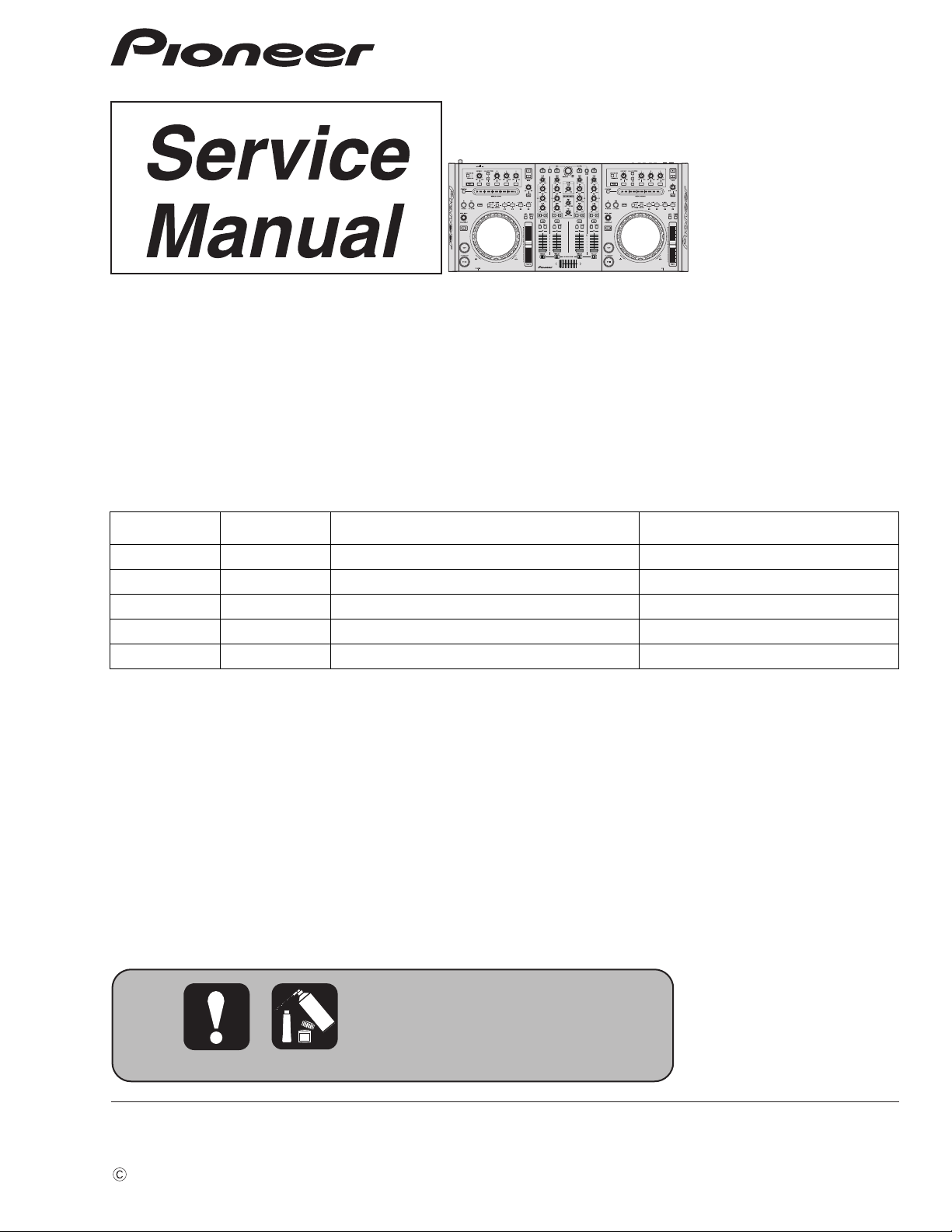
DDJ-T1
For details, refer to "Important Check Points for good servicing".
DJ CONTROLLER
DDJ-T1
THIS MANUAL IS APPLICABLE TO THE FOLLOWING MODEL(S) AND TYPE(S).
Model Type Power Requirement Remarks
DDJ-T1 SVYXJ8 AC 100 V to 240 V
DDJ-T1 UXJCB AC 100 V to 240 V
DDJ-T1 FLPXJ AC 100 V to 240 V
DDJ-T1 KXJ5 AC 100 V to 240 V
DDJ-T1 AXJ5 AC 100 V to 240 V
ORDER NO.
RRV4164
PIONEER CORPORATION 1-1, Shin-ogura, Saiwai-ku, Kawasaki-shi, Kanagawa 212-0031, Japan
PIONEER ELECTRONICS (USA) INC. P.O. Box 1760, Long Beach, CA 90801-1760, U.S.A.
PIONEER EUROPE NV Haven 1087, Keetberglaan 1, 9120 Melsele, Belgium
PIONEER ELECTRONICS ASIACENTRE PTE. LTD. 253 Alexandra Road, #04-01, Singapore 159936
PIONEER CORPORATION
K-IZV FEB.
2011 Printed in Japan
Page 2
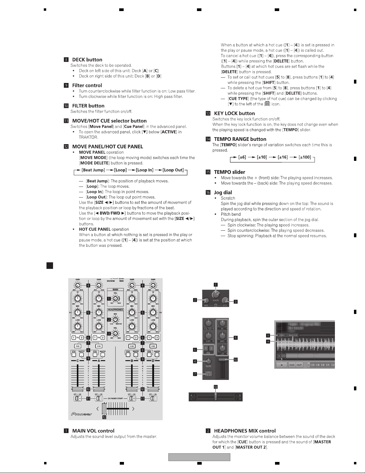
1
WARNING
This product may contain a chemical known to the State of California to cause cancer, or birth defects or other reproductive
harm.
Health & Safety Code Section 25249.6 - Proposition 65
This service manual is intended for qualified service technicians; it is not meant for the casual do-it-
yourselfer. Qualified technicians have the necessary test equipment and tools, and have been trained
to properly and safely repair complex products such as those covered by this manual.
Improperly performed repairs can adversely affect the safety and reliability of the product and may
void the warranty. If you are not qualified to perform the repair of this product properly and safely, you
should not risk trying to do so and refer the repair to a qualified service technician.
1. SAFETY PRECAUTIONS
The following check should be performed for the
continued protection of the customer and service
technician.
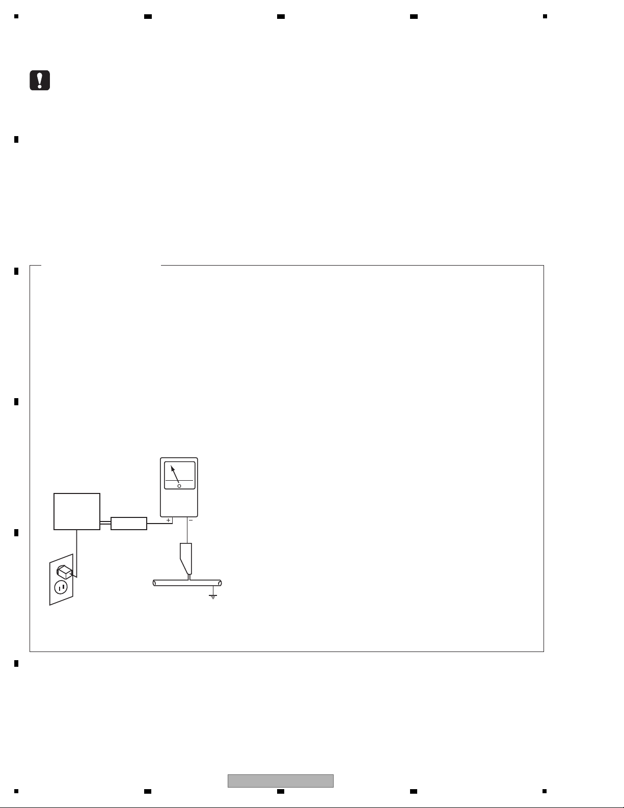
LEAKAGE CURRENT CHECK
Measure leakage current to a known earth ground
(water pipe, conduit, etc.) by connecting a leakage
current tester such as Simpson Model 229-2 or
equivalent between the earth ground and all exposed
metal parts of the appliance (input/output terminals,
screwheads, metal overlays, control shaft, etc.). Plug
the AC line cord of the appliance directly into a 120 V
AC 60 Hz outlet and turn the AC power switch on. Any
current measured must not exceed 0.5 mA.
ANY MEASUREMENTS NOT WITHIN THE LIMITS
OUTLINED ABOVE ARE INDICATIVE OF A POTENTIAL
SHOCK HAZARD AND MUST BE CORRECTED BEFORE
RETURNING THE APPLIANCE TO THE CUSTOMER.
2. PRODUCT SAFETY NOTICE
Many electrical and mechanical parts in the appliance
have special safety related characteristics. These are
often not evident from visual inspection nor the protection
afforded by them necessarily can be obtained by using
replacement components rated for voltage, wattage, etc.
Replacement parts which have these special safety
characteristics are identified in this Service Manual.
Electrical components having such features are
identified by marking with a > on the schematics and on
the parts list in this Service Manual.
The use of a substitute replacement component which
does not have the same safety characteristics as the
PIONEER recommended replacement one, shown in the
parts list in this Service Manual, may create shock, fire,
or other hazards.
Product Safety is continuously under review and new
instructions are issued from time to time. For the latest
information, always consult the current PIONEER Service
Manual. A subscription to, or additional copies of,
PIONEER Service Manual may be obtained at a nominal
charge from PIONEER.
Leakage
current
tester
Reading should
not be above
0.5 mA
Device
under
test
Test all
exposed metal
surfaces
Also test with
plug reversed
(Using AC adapter
plug as required)
Earth
ground
AC Leakage Test
(FOR USA MODEL ONLY)
2 3 4
SAFETY INFORMATION
A
B
C
D
E
F
2
1
2 3 4
DDJ-T1
Page 3
5
[Important Check Points for Good Servicing]
In this manual, procedures that must be performed during repairs are marked with the below symbol.
Please be sure to confirm and follow these procedures.
1. Product safety
Please conform to product regulations (such as safety and radiation regulations), and maintain a safe servicing environment by
following the safety instructions described in this manual.
1 Use specified parts for repair.
Use genuine parts. Be sure to use important parts for safety.
2 Do not perform modifications without proper instructions.
Please follow the specified safety methods when modification(addition/change of parts) is required due to interferences such as
radio/TV interference and foreign noise.
3 Make sure the soldering of repaired locations is properly performed.
When you solder while repairing, please be sure that there are no cold solder and other debris.
Soldering should be finished with the proper quantity. (Refer to the example)
4 Make sure the screws are tightly fastened.
Please be sure that all screws are fastened, and that there are no loose screws.
5 Make sure each connectors are correctly inserted.
Please be sure that all connectors are inserted, and that there are no imperfect insertion.
6 Make sure the wiring cables are set to their original state.
Please replace the wiring and cables to the original state after repairs.
In addition, be sure that there are no pinched wires, etc.
7 Make sure screws and soldering scraps do not remain inside the product.
Please check that neither solder debris nor screws remain inside the product.
8 There should be no semi-broken wires, scratches, melting, etc. on the coating of the power cord.
Damaged power cords may lead to fire accidents, so please be sure that there are no damages.
If you find a damaged power cord, please exchange it with a suitable one.
9 There should be no spark traces or similar marks on the power plug.
When spark traces or similar marks are found on the power supply plug, please check the connection and advise on secure
connections and suitable usage. Please exchange the power cord if necessary.
a Safe environment should be secured during servicing.
When you perform repairs, please pay attention to static electricity, furniture, household articles, etc. in order to prevent injuries.
Please pay attention to your surroundings and repair safely.
2. Adjustments
To keep the original performance of the products, optimum adjustments and confirmation of characteristics within specification.
Adjustments should be performed in accordance with the procedures/instructions described in this manual.
4. Cleaning
For parts that require cleaning, such as optical pickups, tape deck heads, lenses and mirrors used in projection monitors, proper
cleaning should be performed to restore their performances.
3. Lubricants, Glues, and Replacement parts
Use grease and adhesives that are equal to the specified substance.
Make sure the proper amount is applied.
5. Shipping mode and Shipping screws
To protect products from damages or failures during transit, the shipping mode should be set or the shipping screws should be
installed before shipment. Please be sure to follow this method especially if it is specified in this manual.
6 7 8
A
B
C
D
5
DDJ-T1
6 7 8
E
F
3
Page 4

1
2 3 4
CONTENTS
SAFETY INFORMATION ..........................................................................................................................................................2
1. SERVICE PRECAUTIONS ....................................................................................................................................................5
A
B
C
D
E
F
1.1 NOTES ON SOLDERING ...............................................................................................................................................5
1.2 SERVICE NOTICE ..........................................................................................................................................................5
2. SPECIFICATIONS .................................................................................................................................................................6
2.1 SPECIFICATIONS...........................................................................................................................................................6
2.2 PANEL FACILITIES .........................................................................................................................................................7
3. BASIC ITEMS FOR SERVICE.............................................................................................................................................13
3.1 CHECK POINTS AFTER SERVICING..........................................................................................................................13
3.2 JIGS LIST......................................................................................................................................................................13
3.3 PCB LOCATIONS .........................................................................................................................................................14
4. BLOCK DIAGRAM...............................................................................................................................................................16
4.1 OVERALL WIRING DIAGRAM......................................................................................................................................16
4.2 OVERALL BLOCK DIAGRAM.......................................................................................................................................18
4.3 POWER BLOCK DIAGRAM..........................................................................................................................................20
5. DIAGNOSIS.........................................................................................................................................................................22
5.1 POWER ON SEQUENCE .............................................................................................................................................22
5.2 TROUBLESHOOTING ..................................................................................................................................................23
5.3 VOLTAGE MONITORING ..............................................................................................................................................31
5.4 HOW TO CHECK OPERATIONS USING THE TRAKTOR SOFTWARE......................................................................32
6. SERVICE MODE .................................................................................................................................................................36
6.1 OUTLINE OF SERVICE MODE ....................................................................................................................................36
6.2 DETAILS ON SERVICE MODE.....................................................................................................................................37
6.3 ABOUT THE DEVICE ...................................................................................................................................................40
7. DISASSEMBLY ....................................................................................................................................................................41
8. EACH SETTING AND ADJUSTMENT ................................................................................................................................49
8.1 NECESSARY ITEMS TO BE NOTED .................................................................................................
CO
NFIRMATION OF THE VERSIONS OF THE FIRMWARE ......................................................................................49
8.2
..........................49
8.3 UPDATING OF THE FIRMWARE..................................................................................................................................50
8.4 COPYING THE PROGRAM FOR THE USB CONTROLLER .......................................................................................51
8.5 JOG DIAL ROTATION LOAD ADJUSTMENT ...............................................................................................................52
9. EXPLODED VIEWS AND PARTS LIST ...............................................................................................................................54
9.1 PACKING SECTION......................................................................................................................................................54
9.2 EXTERIOR SECION .....................................................................................................................................................56
9.5 JOG SECTION..............................................................................................................................................................62
10. SCHEMATIC DIAGRAM ....................................................................................................................................................64
10.1 JACB ASSY.................................................................................................................................................................64
10.2 UCOM ASSY (1/6) ......................................................................................................................................................66
10.3 UCOM ASSY (2/6) ......................................................................................................................................................68
10.4 UCOM ASSY (3/6) ......................................................................................................................................................70
10.5 UCOM ASSY (4/6) ......................................................................................................................................................72
10.6 UCOM ASSY (5/6) ......................................................................................................................................................74
10.7 UCOM ASSY (6/6) ......................................................................................................................................................76
10.8 CDCB 1, CDCB 2, TCHB and JOGB ASSYS .............................................................................................................78
................................................................................................................................................................80
10.9 LEDB A
SSY
10.10 CDJ1B ASSY ............................................................................................................................................................82
10.11 CDJ2B ASSY ............................................................................................................................................................84
10.12 DJMB ASSY..............................................................................................................................................................86
10.13 MICB ASSY...............................................................................................................................................................88
10.14 CHFD, CRFD and HPJK ASSYS ..............................................................................................................................90
10.15 USBB ASSY..............................................................................................................................................................92
10.16 VOLTAGES................................................................................................................................................................94
10.17 WAVEFORMS ...........................................................................................................................................................95
11. PCB CONNECTION DIAGRAM ......................................................................................................................................100
11.1 JACB ASSY...............................................................................................................................................................100
11.2 UCOM ASSY.............................................................................................................................................................102
11.3 CDCB 1 ASSY ..........................................................................................................................................................106
11.4 CDCB 2 ASSY ..........................................................................................................................................................107
CHB
11.5 T
, JOGB and LEDB ASSYS ..............................................................................................................................108
11.6 CDJ1B ASSY ............................................................................................................................................................112
11.7 CDJ2B ASSY ............................................................................................................................................................116
11.8 DJMB ASSY..............................................................................................................................................................120
11.9 CHFD and CRFD ASSYS .........................................................................................................................................124
11.10 MICB ASSY.............................................................................................................................................................128
11.11 HPJK ASSY ............................................................................................................................................................129
11.12 USBB ASSY............................................................................................................................................................130
12. PCB PARTS LIST ............................................................................................................................................................131
4
1
2 3 4
DDJ-T1
Page 5

5
• For environmental protection, lead-free solder is used on the printed circuit boards mounted in this unit.
Be sure to use lead-free solder and a soldering iron that can meet specifications for use with lead-free solders for repairs
accompanied by reworking of soldering.
• Compared with conventional eutectic solders, lead-free solders have higher melting points, by approximately 40 ºC.
Therefore, for lead-free soldering, the tip temperature of a soldering iron must be set to around 373 ºC in general, although
the temperature depends on the heat capacity of the PC board on which reworking is required and the weight of the tip of
the soldering iron.
Do NOT use a soldering iron whose tip temperature cannot be controlled.
Compared with eutectic solders, lead-free solders have higher bond strengths but slower wetting times and higher melting
temperatures (hard to melt/easy to harden).
The following lead-free solders are available as service parts:
• Parts numbers of lead-free solder:
GYP1006 1.0 in dia.
GYP1007 0.6 in dia.
GYP1008 0.3 in dia.
• For checking of audio and operating elements, the DJ application (TRAKTOR) included with this product is used.
TRAKTOR must be installed in your PC. For details on installation, see "5.4 HOW TO CHECK OPERATIONS USING
THE TRAKTOR SOFTWARE."
For connection of this product with a PC, be sure to use the supplied USB cable (registered jig tool), whose operation
with this product is guaranteed.
Voltage Monitoring
This unit always monitors for power failure and will shut itself off immediately after an error is detected. All LEDs are unlit after
an error is generated. After the unit shuts itself off because of an error, disconnect the AC adapter and USB cable and wait at
least 1 minute before turning the unit back on. Repair the unit according to the diagnostic procedures described in
“5.3 VOLTAGE MONITORING.”
Limitations when the unit is operating on USB-bus power
There are some limitations in operations of this unit while it is operated on USB-bus power, as shown below.
• The JOG dial indicator does not light.
• Lighting of the indicators (excluding that for the JOG dial) becomes dim.
• The AUX IN and MIC connectors are disabled.
• The sound volume through the headphones is reduced.
On the EEPROM on the UCOM ASSY
No program has been stored in the EEPROM (IC2003) on the UCOM Assy (blank ROM) when it is supplied as a part for
service.
After the EEPROM is replaced, be sure to copy the program for the USB controller to it. For details, see “8.4 Copying the
Program for the USB Controller.”
Replacement of the MAIN_UCOM
When replacement of the MAIN_UCOM (IC701) is required, order a microcomputer dedicated for service (PEG850A8-K).
6 7 8
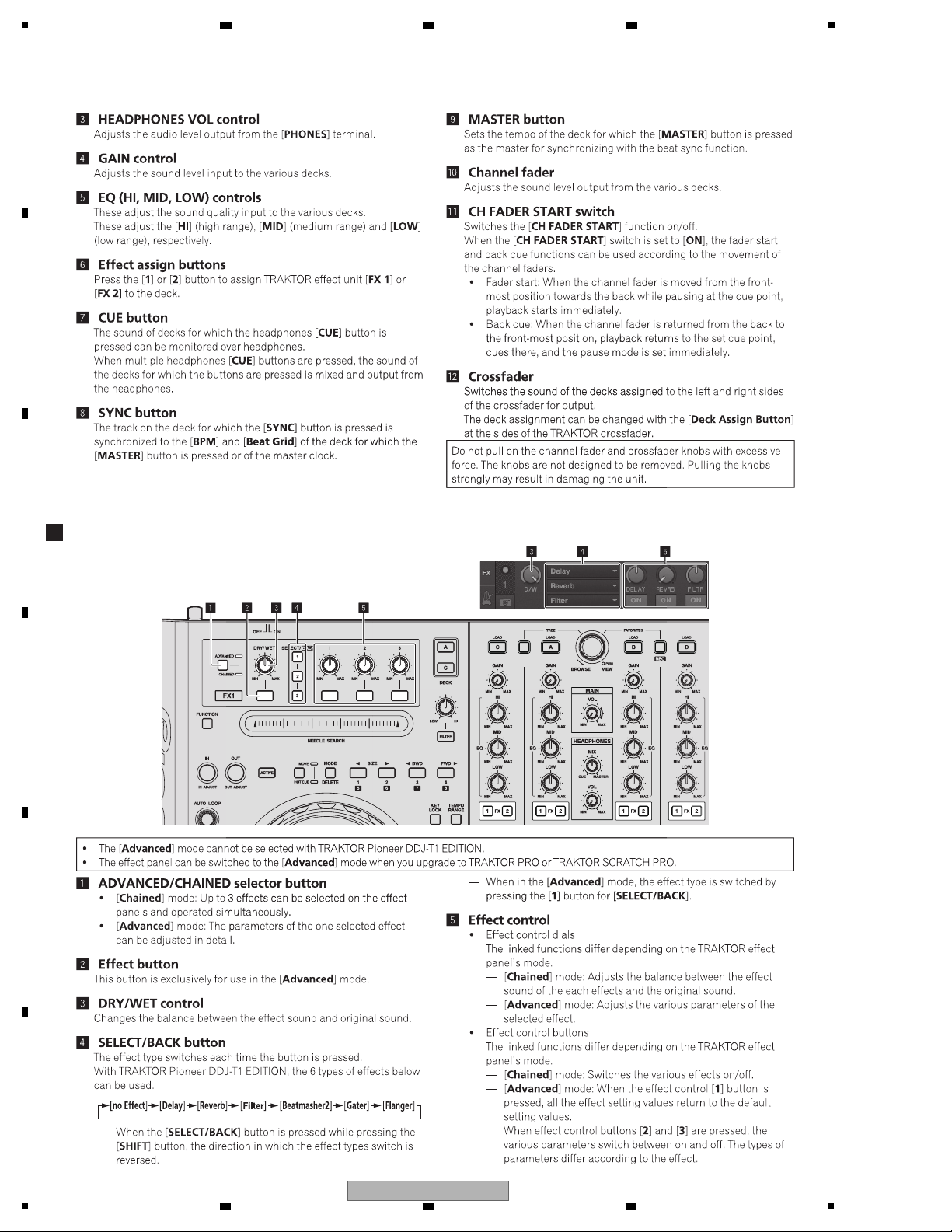
1. SERVICE PRECAUTIONS
1.1 NOTES ON SOLDERING
A
B
1.2 SERVICE NOTICE
DDJ-T1
5
6 7 8
C
D
E
F
5
Page 6
1
AC adapter
Power..................................AC 100 V to 240 V, 50 Hz/ 60 Hz
Rated current.............................................................300 mA
Rated output........................................................DC 5 V, 2 A
General – Main Unit
Power consumption (when using AC adapter)...........700 mA
Power consumption (when using USB bus power)....500 mA
Main unit weight.............................................4.9 kg (10.8 lb)
Max. dimensions.....680 mm (W) × 95.2 mm (H) × 317.7 mm (D)
(26.8 in. (W) × 3.7 in. (H) × 12.5 in. (D))
Tolerable operating temperature......+5 °C to +35 °C (+41 °F to +95 °F)
Tolerable operating humidity..................5 % to 85 % (no condensation)
Audio Section
Rated output level
MASTER OUT 1.................................................4.2 Vrms
MASTER OUT 2.................................................2.1 Vrms
Total harmonic distortion
MASTER OUT 1..................................................0.006 %
MASTER OUT 2..................................................0.006 %
Frequency characteristic
MASTER OUT 1......................................20 Hz to 20 kHz
MASTER OUT 2......................................20 Hz to 20 kHz
S/ N ratio (when playing on computer)
MASTER OUT 1.........103 dB or greater (at rated output)
MASTER OUT 2.........103 dB or greater (at rated output)
Input impedance
AUX..........................................................................24 kΩ
MIC..........................................................................10 kΩ
Output impedance
MASTER OUT 1............................................1 kΩ or less
MASTER OUT 2............................................1 kΩ or less
PHONES...................................................................41 Ω
Input / Output terminals
USB terminal
B type...................................................................1 set
MASTER OUT 1 output terminal
TRS phone jack (Ø 6.3 mm).................................1 set
MASTER OUT 2 output terminal
RCA pin jacks.....................................................1 sets
PHONES output terminal
Stereo phone jack (Ø 6.3 mm).............................1 set
Stereo mini phone jack (Ø 3.5 mm)......................1 set
AUX input terminal
RCA pin jack.......................................................1 sets
MIC input terminal
Phone jack (Ø 6.3 mm).........................................1 set
• For improvement purposes, specifications and design of
this unit and the included software are subject to change
without notice.
• TRAKTOR Pioneer DDJ-T1 EDITION software CD-ROM
(DXX2665)
• Driver software CD-ROM
(DXX2666)
• USB cable
(DDE1140)
• Operating instructions
(SVYXJ8: DRB1537, DRB1563)
(UXJCB: DRB1536)
(FLPXJ: DRB1539)
(KXJ5: DRB1541)
(AXJ5: DRB1540)
Accessories
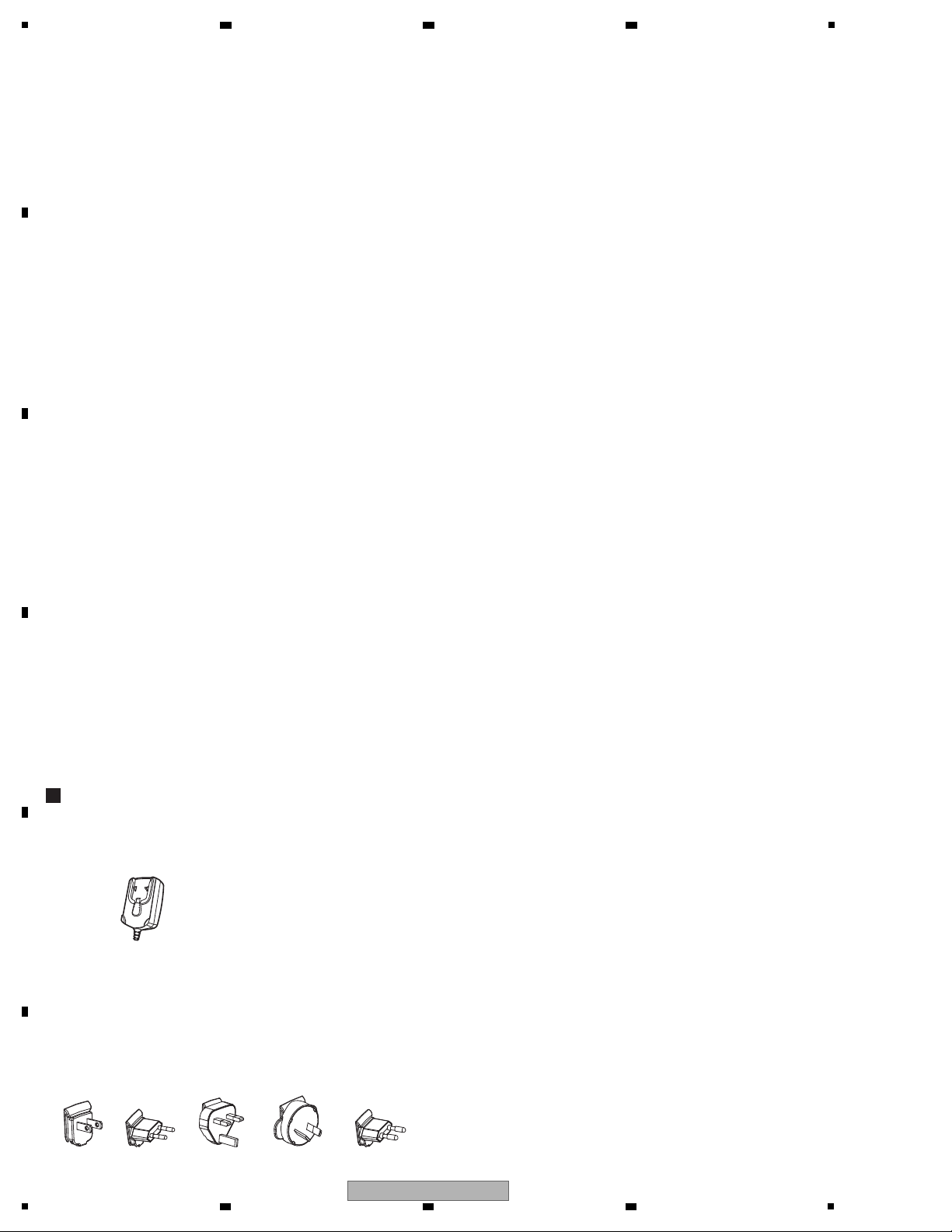
• AC adapter
(DWR1491)
• Power plug
(SVYXJ8: DKX1048, DKX1049)
(UXJCB: DKX1047)
(FLPXJ: DKX1048, DKX1049, DKX1047, DKX1050, DKX1051)
(KXJ5: DKX1051)
(AXJ5: DKX1052)
2. SPECIFICATIONS
2.1 SPECIFICATIONS
A
2 3 4
B
C
D
E
F
6
1
2 3 4
DDJ-T1
Page 7
Rear panel
Front panel
5
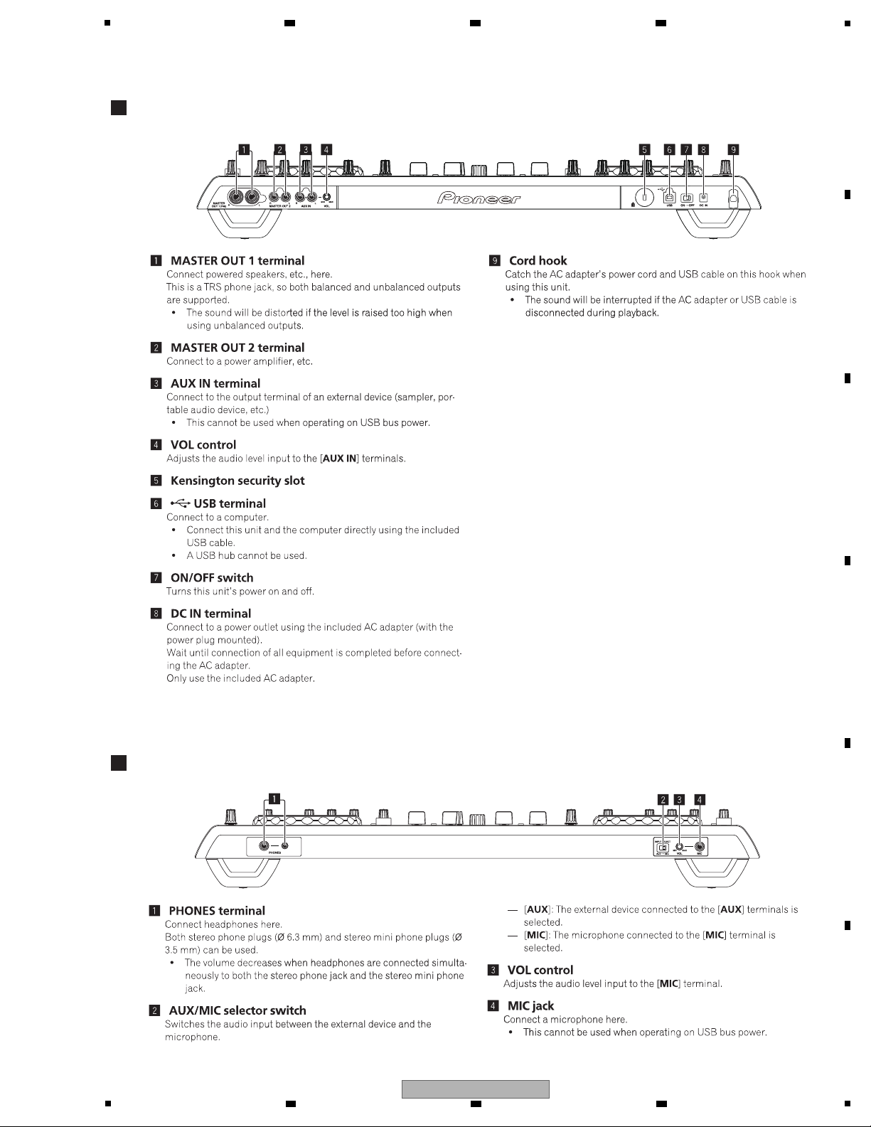
2.2 PANEL FACILITIES
6 7 8
A
B
C
D
E
F
DDJ-T1
5
6 7 8
7
Page 8
1
Control panel
A
B
2 3 4
C
D
E
F
8
1
2 3 4
DDJ-T1
Page 9
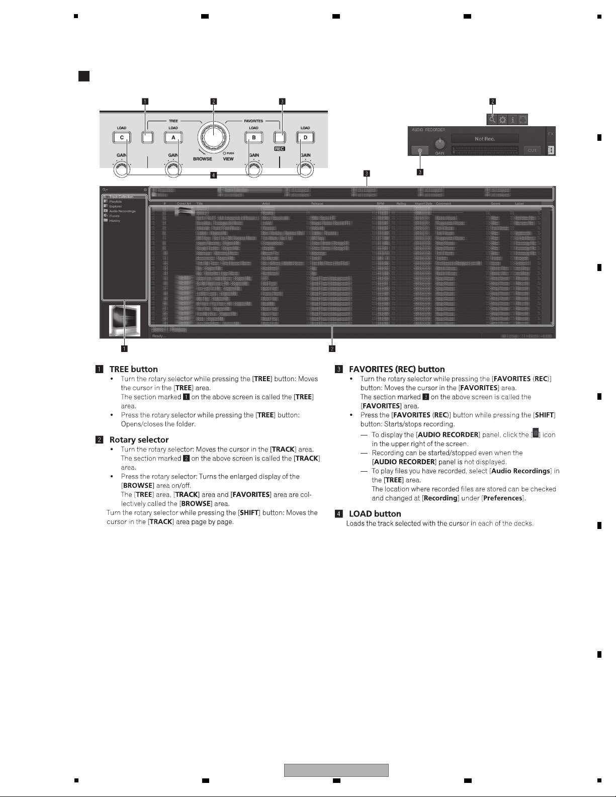
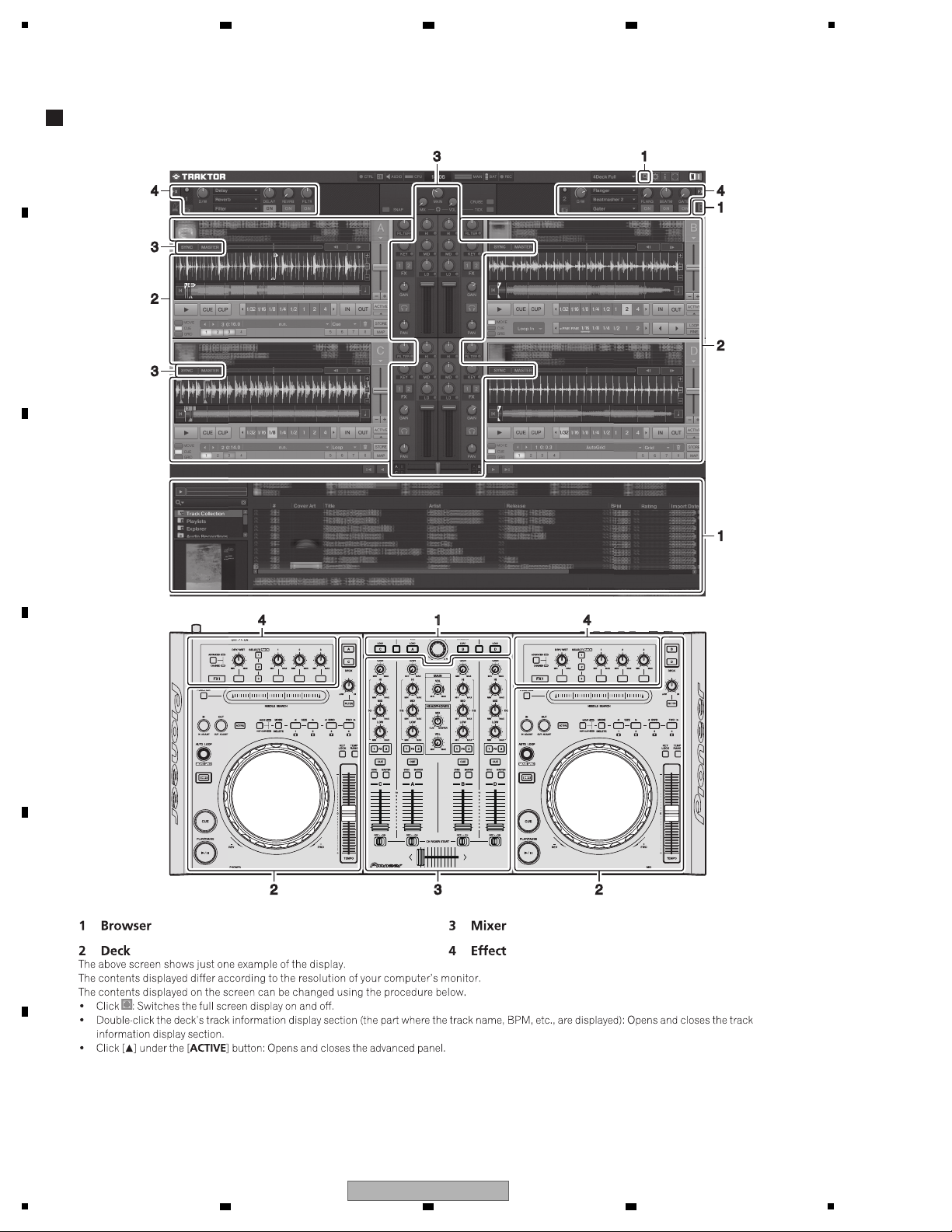
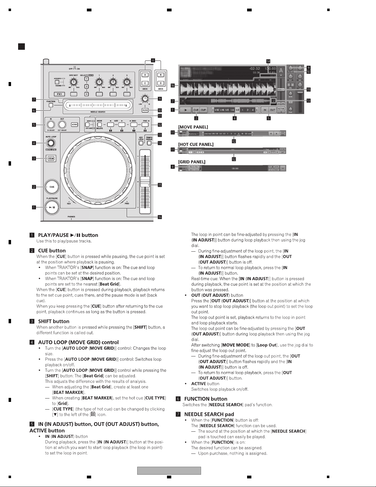
1 Browser
5
6 7 8
A
B
C
D
E
F
DDJ-T1
5
6 7 8
9
Page 10
A
2 Deck
B
1
2 3 4
C
D
E
F
10
1
2 3 4
DDJ-T1
Page 11
5
3 Mixer
6 7 8
A
B
C
D
E
F
DDJ-T1
5
6 7 8
11
Page 12
1
4 Effect
A
B
2 3 4
C
D
E
F
12
1
2 3 4
DDJ-T1
Page 13
5
No.
Procedures Check points
1
2
3
4
5
7
6
Confirm that the customer complaint has been resolved.
If the problem pointed out by the customer occurs with a
specific source or operation, such as PC input, AUX/MIC input,
Fader, or VOL, input that specific source then perform that
specific operation for checking.
The customer complain must not be reappeared.
Audio and operations must be normal.
Confirmation of operation of operating elements 1
Enter Service mode.
There must be no errors in operations of each button, LED, the
JOG dial, and NeedleSearch.
Confirmation of operation of operating elements 2
Connect this unit with a PC with the DJ application (TRAKTOR)
installed, via USB.
There must be no errors in operations of volume controls,
faders, and rotary encoders.
Check the analog audio output.
Connect this unit with a PC with the DJ application (TRAKTOR)
installed, via USB, then play back audio
There must be no errors, such as noise, in audio signals and
operations of the MASTER/HEADPHONES outputs.
Check the analog audio input.
Input an audio signal via AUX/MIC. (Make the input settings,
referring to “Inputting Audio from Microphones or External
Equipment” in the Operating Instructions.)
Audio and operations must be normal.
Check the appearance of the product.
No scratches or dirt on its appearance after receiving it for
service.
Confirmation of USB-bus Power
Disconnect the AC adapter and operate the unit only on
USB-bus power.
Audio and operations must be normal.
(For details on limitations of USB-bus power, refer to the
Operating Instructions.)
Item to be checked regarding audio
Distortion
Noise
Volume too low
Volume too high
Volume fluctuating
Sound interrupted
Items to be checked after servicing
To keep the product quality after servicing, confirm recommended check points shown below.
See the table below for the items to be checked regarding audio.
Lubricants and Glues List
Name Part No. Remarks
Lubricating oil GYA1001 Refer to “9.5 JOG SECTION”.
Jigs List
Jig Name Part No. Purpose of use / Remarks
USB cable GGP1188 for PC connection, accessory
AC adapter DWR1491 Accessory (Note: The power plug part is different.)
6 7 8
3. BASIC ITEMS FOR SERVICE
3.1 CHECK POINTS AFTER SERVICING
A
B
3.2 JIGS LIST
C
D
E
5
6 7 8
DDJ-T1
F
13
Page 14
1
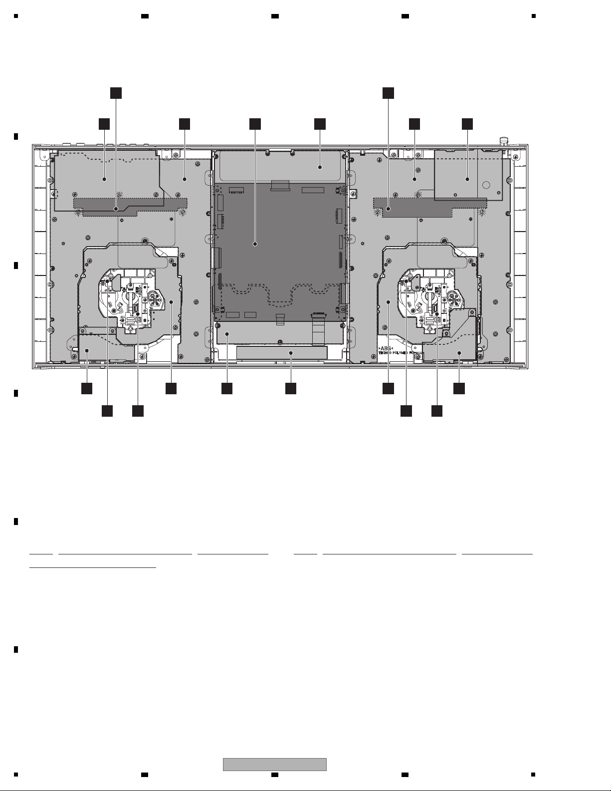
NSP 1..MAIN ASSY DWM2421
2..UCOM ASSY DWX3209
2..CDCB 1 ASSY DWX3210
2..CDCB 2 ASSY DWX3224
NSP 1..CDJ1 ASSY DWM2422
2..CDJ1B ASSY DWS1430
2..JOGB ASSY DWS1432
2..TCHB ASSY DWS1433
2..LEDB ASSY DWS1434
NSP 1..CDJ2 ASSY DWM2423
2..CDJ2B ASSY DWS1431
2..JOGB ASSY DWS1432
2..TCHB ASSY DWS1433
2..LEDB ASSY DWS1434
NSP 1..DJM1 ASSY DWM2424
2..CHFD ASSY DWX3212
2..CRFD ASSY DWX3213
2..MICB ASSY DWX3215
2..HPJK ASSY DWX3216
NSP 1..DJM2 ASSY DWM2426
2..DJMB ASSY DWX3211
2..JACB ASSY DWX3214
2..USBB ASSY DWX3222
A
JACB ASSY
D
CDCB 1 ASSY/CDCB 2 ASSY
(DWX3210/DWX3224)
Either the CDCB 1 Assy or CDCB 2 Assy is assembled here. The CDCB 1 Assy
and CDCB 2 Assy are interchangeably used and handled similarly in their production
management.
Either the CDCB 1 Assy or CDCB 2 Assy is assembled here. The CDCB 1 Assy
and CDCB 2 Assy are interchangeably used and handled similarly in their production
management.
C
CDCB 1 ASSY/CDCB 2 ASSY
(DWX3210/DWX3224)
K
MICB ASSY
E
TCHB ASSY
F
JOGB ASSY
F
JOGB ASSY
E
TCHB ASSY
M
CRFD ASSY
• Bottom view
L
CHFD ASSY
N
HPJK ASSY
G
LEDB
ASSY
G
LEDB
ASSY
O
USBB ASSY
H
CDJ1B
ASSY
I
CDJ2B ASSY
J
DJMB ASSY
B
UCOM ASSY
Mark No. Description Part No. Mark No. Description Part No.
LIST OF ASSEMBLIES
NOTES: - Parts marked by “NSP” are generally unavailable because they are not in our Master Spare Parts List.
-
The > mark found on some component parts indicates the importance of the safety factor of the part.
Therefore, when replacing, be sure to use parts of identical designation.
3.3 PCB LOCATIONS
A
2 3 4
B
C
D
E
F
14
1
2 3 4
DDJ-T1
Page 15

5
6 7 8
A
B
C
D
E
F
DDJ-T1
5
6 7 8
15
Page 16
1
CN2001/CN2101
C D
CDCB 1 ASSY/CDCB 2 ASSY
(DWX3210/DWX3224)
/
MAIN ucom
M16C/65 128Pin
R5F3651ENFC
IC701
DYW1801-/J
PEG850A8-K
A
JACB ASSY
(DWX3214)
AUX IN
MASTER2 OUT
MASTER1_R OUT
MASTER1_L OUT
HP OUT
HP OUT (mini)
CDC_CS1
GND_D
CDC_SCLK
CDC_DSI
CDC_DSO
V+3R3_D
CDC_INT1
MUTE
V+6
V-6
GND_P
MASTER_L
GND_AM
GND_AM
V-6
V+6
GND_P
AUX_R_IN
GND_AA
AUX_L_IN
GND_AA
GND_D
LED_3
LED_5
GND_D
LED_4
LED_0
LED_2
GRID3
LED_1
GRID1
GRID2
GRID0
GND_D
JOG1_2
V+5_D
JOG_TCH_1
GND_D
JOG1_1
V+5_D
V+3R3_D
JOG1/2_1
JOG1/2_2
V+3R3_D
GND_D
V+3R3_D
JOG_TCH_1/2
GND_D
GRID2
GRID5
GND_D
GND_D
GRID7
GRID6
GRID3
GND_D
LED_14
GRID1
LED_12
GRID0
LED_13
GRID4
KEY_IN12
CUR_ENC1
GND_D
GND_D
KEY_IN11
KEY_IN9
KEY_IN10
CUR_ENC2
AD_SW_A
V+5_D
AD_4
AD_3
GND_AD
AD_1
AD_0
AD_2
GND_AD
V+3R3_AD
GND_D
V+6
HP_L
GND_P
V-6
GND_P
HP_R
GND_AH
GND_AH
MUTE
AD_SW_B
JOG_TCH_1
GRID4
GRID5
GRID6
GRID7
GND_D
KEY_IN1
KEY_IN2
KEY_IN3
KEY_IN4
GND_D
GND_D
LED_0
LED_1
GND_D
LED_2
LED_3
LED_4
LED_5
L_ENC1_1
L_ENC1_2
GND_D
GND_AD
GND_AM
MASTER_R
AD_DRYWET1
AD_EFF1_2
GND_AD
AD_EFF1_3
AD_EFF1_1
AD_FILTER1
AD_PITCH1_1
GND_AD
V+3R3_AD
AD_PITCH1_2
GND_AD
V+5_D
V+5_D
GRID0
GRID1
GRID2
GRID3
GND_D
JOG1_2
JOG1_1
V+3R3_D
GND_AM
CN902
AKM1294-
1234567
8
CN4402
KM200NA7L
1
V-6A
2
V+6A
3
GND_PA
4
AUX_IN_R
5
6
AUX_IN_L
7
CN302
AKM1293-
1234567
CN3002
VKN 1256-
1
2
3
4
5
6
7
8
9
10
11
12
13
14
15
16
17
18
19
20
21
22
23
24
25
CN3001
VKN 1250-
1
2
3
4
5
6
7
8
9
10
11
12
13
14
15
16
17
18
19
CN6001
VKN 1279-
1
2
3
4
5
6
7
8
9
10
11
12
13
LED_1/7
14
LED_0/6
15
LED_2/8
16
17
LED_4/10
18
LED_3/9
19
LED_5/11
CN6002
KM200NA4L
1
2
3
4
PF04PG-B05
CN3201
123
4
51048-0300
JH6001
123
CN3301
52151-0310
1
2
3
CN1002
VKN 1300-
1234567
8
CN4001
VKN 1239-
1234567
8
JA4403
AKB7181-
54321
CN4801
KM200NA9
123456789
JA4802
CKS4124-
2
3
1
JA4801
DKN1622-
2
3
1
JA4404
DKN1622-
231
JA4402
DKN1622-
231
JA4401
AKB7181-
54321
VKN 1429-A
CN1001
123456789
101112131415161718192021222324
25
CN4002
VKN 1256-
123456789
101112
131415161718192021
222324
25
CN1004
AKM1299-
123456789
10
CN906
VKN 1424-
1
2
3
4
5
6
7
8
9
10
11
12
13
14
15
16
17
18
19
20
AKM1279-
1
CDC_INT
2
CDC_CS
3
GND_CDC
4
5
GD_CDC
6
7
8
V+3R3_CDC
CN3003
VKN 1251-
1
2
3
4
5
6
7
8
9
10
11
12
13
14
15
16
17
18
19
20
CN301
AKM1295-
1
2
3456789
CN4401
KM200NA9L
123456789
CN501
AKM1295-
1
2
34567
8
9
VKN 1429-A
CN905
1
2
3
4
5
6
7
8
9
10
11
12
13
14
15
16
17
18
19
20
21
22
23
24
25
B2PS-VH
CN4403
1
2
DKP38942mm pitch
L=100mm
DKP39202mm pitch
L=210mm
DKP38972mm pitch
L=360mm
DKP39232mm pitch
L=610mm
FFC
DDD15431mm pitch /
L=90mm/
TAPE LENGTH=7mm
FFC
DDD15611mm pitch /
L=270mm/
TAPE LENGTH=8mm
FFC
DDD15451mm pitch /
L=130mm/
TAPE LENGTH=8mm
FFC
DDD15471mm pitch /
L=100mm/TAPE LENGTH=8mm,1
HP OUT
USB
AUX IN
MASTER OUT
CDC
SW
EEPROM
IC201
+
-
OP AMP
+
-
OP AMP
CERAMIC
X701
RESET IC
IC106
OP AMP
+
-
+
OP AMP
-
+
OP AMP
-
+
OP AMP
-
LED/KEY
MATRIX
VOL INPUT
LED/KEY MATRIX
VOL INPUT
LED/KEY MATRIX
VOL INPUT
LED/KEY MATR
FFC
DDD15431mm pitch /
L=90mm/
TAPE LENGTH=7mm
JP501
DKP3926-
3.96mm pitch
L=220mm
G
LEDB ASSY
(DWS1434)
E
TCHB ASSY
(DWS1433)
F
N
JOGB ASSY
(DWS1432)
HPJK ASSY
(DWX3216)
J
DJMB ASSY
(DWX3211)
H
CDJ1B ASSY
(DWS1430)
UCOM ASSY
(DWX3209)
B
B B
1/6- 6/6
Either the CDCB 1 Assy or CDCB 2 Assy is assembled here. The CDCB 1 Assy
and CDCB 2 Assy are interchangeably used and handled similarly in their production
management.
2 3 4
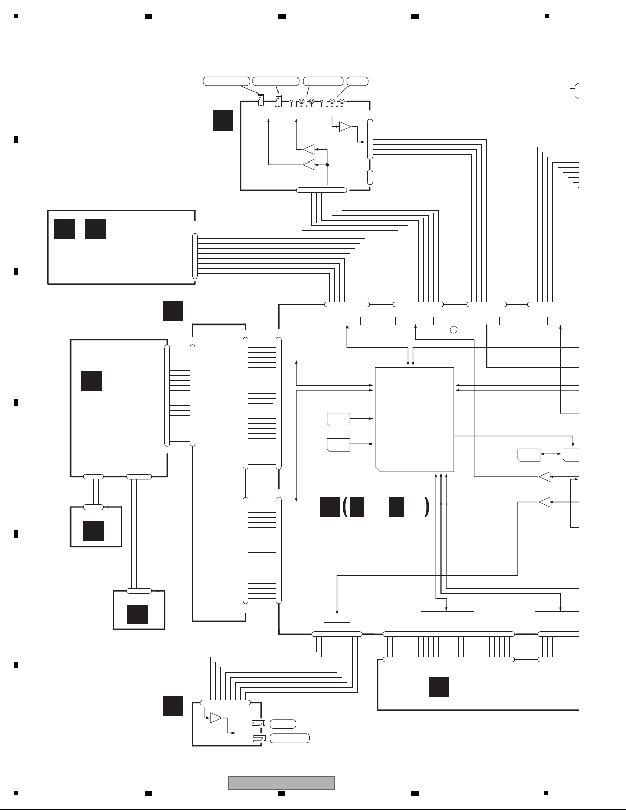
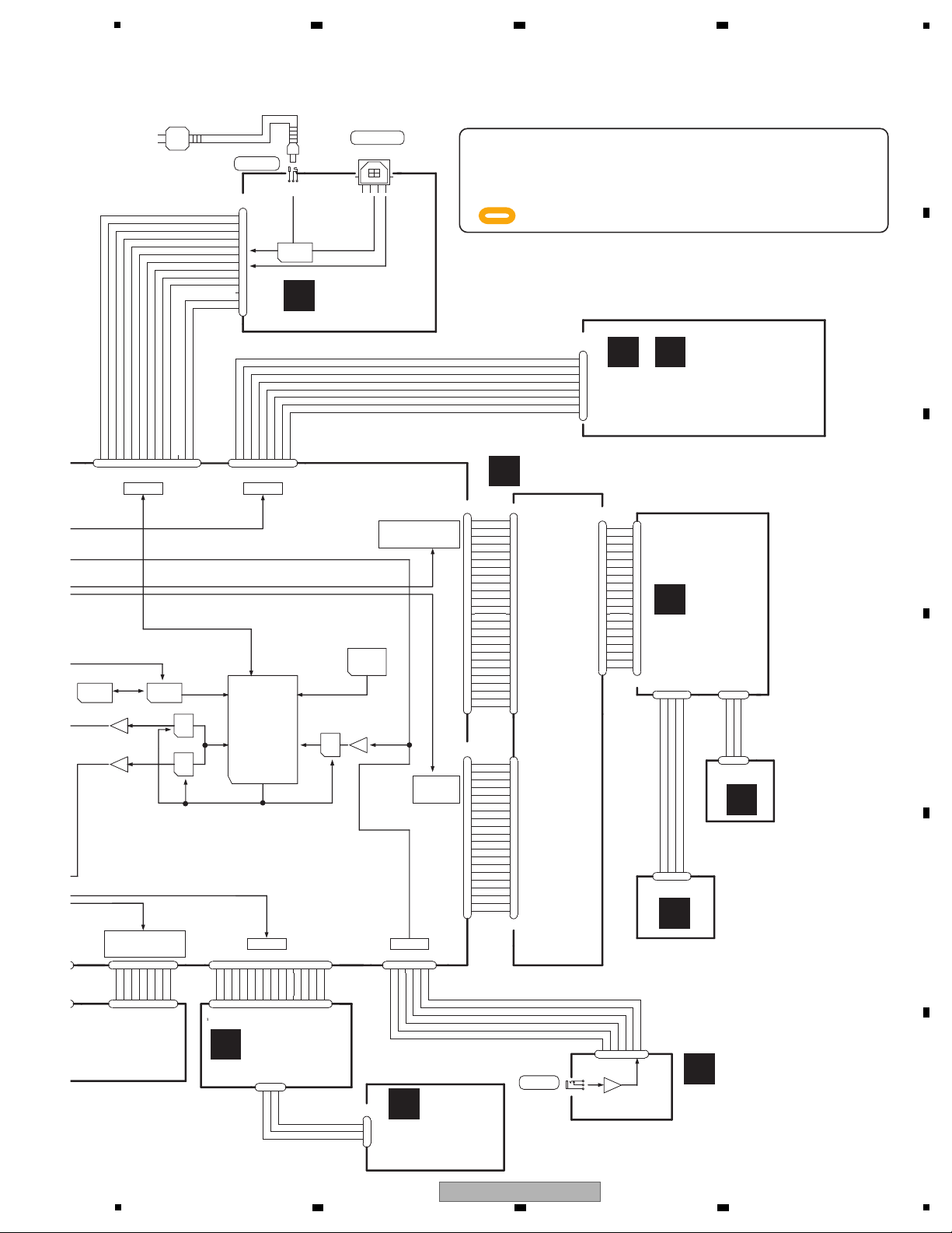
4. BLOCK DIAGRAM
4.1 OVERALL WIRING DIAGRAM
A
B
C
D
E
F
16
1
DDJ-T1
2 3 4
Page 17
5
CN2001/CN 2101
C D
CDCB 1 ASSY/CDCB 2 ASSY
(DWX3210/DWX3224)
/
MIC IN
USB B TYPE
DC JACK
CDC_DSO
CDC_DSI
GND_D
CDC_SCLK
GND_D
CDC_CS2
CDC_INT2
V+5_D
V+5_D
GND_D
V+4R7_STB
ADP_DET
P_SW1_ADP
P_SW2_USB
GND_D2
USB_DP
USB_DN
GND_D
JOG_TCH_2
GRID6
GRID7
GND_D
KEY_IN5
GRID5
GND_D
GRID4
KEY_IN8
LED_7
GND_D
GND_D
KEY_IN6
KEY_IN7
LED_9
LED_6
LED_8
GND_D
LED_11
LED_10
LED_11
LED_9
GND_D
LED_10
LED_8
LED_6
LED_7
GRID2
GND_D
GRID3
GRID0
GRID1
V+5_D
V+5_D
GND_D
JOG2_2
JOG2_1
V+3R3_D
JOG_TCH_2
JOG1/2_1
JOG1/2_2
GND_D
JOG_TCH_1/2
GND_D
V+3R3_D
AD_4
AD_3
GND_AD
AD_1
AD_0
AD_2
GND_AD
V+3R3_AD
KEY_IN13
GND_D
GRID3
GRID2
GRID1
GRID0
GND_D
GND_AD
AD_CROSSF
AD_FADER_C
AD_FADER_D
GND_AD
AD_FADER_B
AD_FADER_A
V+3R3_AD
GND_AD
AD_CROSSF
V+3R3_AD
V+3R3_D
V+6
MIC_IN
GND_P
GND_A
MIC_AUX_DET
V-6
V+5_USB
V+3R3_D
V+3R3_D
JOG2_1
JOG2_2
GND_D
L_ENC2_2
L_ENC2_1
GND_D
GRID3
GRID2
GRID1
GRID0
V+5_D
V+5_D
GND_AD
V+3R3_AD
AD_PITCH2_2
AD_PITCH2_1
GND_AD
AD_FILTER2
AD_DRYWET2
GND_AD
AD_EFF2_3
AD_EFF2_2
AD_EFF2_1
GND_AD
CN3501
VKN 1250-
1
2
3
4
5
6
7
8
9
10
11
12
13
14
15
16
17
18
19
CN6001
VKN 1279-
1
2
3
4
5
6
7
8
9
10
11
12
13
LED_1/7
14
LED_0/6
15
LED_2/8
16
17
LED_4/10
18
LED_3/9
19
LED_5/11
CN6002
KM200NA4L
1
2
3
4
PF04PG-B05
CN3201
123
4
51048-0300
JH6001
123
CN3301
52151-0310
1
2
3
CN1002
VKN 1300-
1234567
8
CN4001
VKN 1239-
1234567
8
CN1003
VKN 1307-
123456789
1011121314
15
CN4201
VKN 1246-
123456789
101112
131415
CN4202
KM200NA3L
123
CN4301
KM200NA3L
1
2
3
CN3502
VKN 1256-
1
2
3
4
5
6
7
8
9
10
11
12
13
14
15
16
17
18
19
20
21
22
23
24
25
JA2502
DKN1237-
1
2
3
4
RT1
RT2
JA2501
DKN1523-
2
3
1
KM200NA6
CN4601
1
2
345
6
CN303
AKM1292-
1
2
345
6
JA4601
DKN1614-
2
3
1
CN1004
AKM1299-
123456789
101112
13
KM200NA13L
CN2501
1
2
3
4
5
6
7
8
9
10
11
12
13
CN904
VKN 1242-
1
2
3
4
5
6
7
8
9
10
11
12
13
14
15
16
17
18
19
20
AKM1279-
1
CDC_INT
2
CDC_CS
3
GND_CDC
4
5
GND_CDC
6
7
8
V+3R3_CDC
CN3503
VKN 1251-
1
2
3
4
5
6
7
8
9
10
11
12
13
14
15
16
17
18
19
20
CN901
AKM1294-
1234567
8
VKN 1429-A
CN903
1
2
3
4
5
6
7
8
9
10
11
12
13
14
15
16
17
18
19
20
21
22
23
24
25
DKP39002mm pitch
L=190mm
DKP39212mm pitch
L=260mm
DKP39222mm pitch
L=210mm
FFC
DDD15431mm pitch /
L=90mm/
TAPE LENGTH=7mm
FFC
DDD15611mm pitch /
L=270mm/
TAPE LENGTH=8mm
FFC
DDD15451mm pitch /
L=130mm/
TAPE LENGTH=8mm
FFC
DDD15471mm pitch /
L=100mm/TAPE LENGTH=8mm,15mm
FFC
DDD1548-
mm pitch /
L=85mm/TAPE LENGTH=6mm.15mm
PF03PP-C06
2mm pitch
L=60mm
USBucom
TUSB3200A
IC202
CHFD
MIC IN
CDC
USB
SW
EEPROM
IC201
Xtail
6MHz
X201
DAC1
DAC2
ADC
+
-
SWITCHED
OP AMP
+
-
OP AMP
+
-
OP AMP
-
+
OP AMP
FET SW
V+5_D
V+5_USB
LED/KEY
MATRIX
VOL INPUT
LED/KEY MATRIX
AC ADAPTER
VOL INPUT
LED/KEY MATRIX
O
USBB ASSY
(DWX3222)
G
LEDB ASSY
(DWS1434)
E
TCHB ASSY
(DWS1433)
F
JOGB ASSY
(DWS1432)
L
CHFD ASSY
(DWX3212)
M
CRFD ASSY
(DWX3213)
K
MICB ASSY
(DWX3215)
I
CDJ2B ASSY
(DWS1431)
-
When ordering service parts, be sure to refer to "EXPLODED VIEWS
and PARTS LIST" or "PCB PARTS LIST".
-
The > mark found on some component parts indicates the importance
of the safety factor of the part.
Therefore, when replacing, be sure to use parts of identical designation.
-
: The power supply is shown with the marked box.
Either the CDCB 1 Assy or CDCB 2 Assy is assembled here. The CDCB 1 Assy
and CDCB 2 Assy are interchangeably used and handled similarly in their production
management.
6 7 8
A
5
DDJ-T1
6 7 8
B
C
D
E
F
17
Page 18
1
A
JACB ASSY
B
UCOM AS
K
MICB ASSY
J
N
G
HPJK ASSY
LEDB ASSY
I
CDJ2B ASSY
E
TCHB ASSY
F
JOGB ASSY
JA4402
Master1 L
Lch
Lch
Lch
Rch
Rch
L-
L+
R+
JA4404
Master1 R
Rch
R-
JA4403
CN4403
GND_AM
Master2
JA4401
Lch
AUX IN
GND_AM
Rch
1044RV
Lch
JA4801
S2I
)niP9(103NC
HP JACK
Lch
Rch
HP L
Lch
HP R
Rch
Rch
JA4802
KCAJiniM
suBS2IS2I
CN901(8Pin)
SPI Bus (CDC)
CN903(25Pin)
JOG2_1/2_2
JOG LED
]0:7[dirG
]0:3[dirG
Trim / Fader
CN904(20Pin)
Grid[7:4]
Key In [12:9][4:1]
Key In[8:5]
Key In[13][8:5]
LED[11:6]
S2I
2_HCT_GOJ
Rch
T
Lch
CN4601
JA4601
MIC IN
IC506
Master
DAC
IC304
Headphone
DAC
IC303
AUX/MIC
ADC
3
3
3
4
3
3
IC101
DC/DC Conv.
IC702
3-8 Decoder
IC1101
Key Buffer
IC1102
Key Buffer
IC301
IC302
IC501
IC305
3
5
1
7
11
10
11
10
3
5
1
7
3
5
5
9
Master R
Master L
5
5
7
2
7
2
1
4
6
2
AUX R In
AUX L In
4
MIC In
IC2001/2101
CDC
Neadle Search
5
9
6
4
CN501(9Pin)
1
7
3
5
1
7
3
5
2044CI1044CI
3
2
3
2
5
2
7
1
IC4405
5
2
7
1
IC4403
5
3
7
1
IC4404
3
5
1
7
IC4801
3
5
3
2
3
2
1
7
3
5
IC4601
4
CN4001
CN3201
CN3301
CN3502
CN3503
CN3501
JH6001
CN6002
CN6001
SWICSW
IC
VOL
AUX/MIC SW
JOG
LED
MATRIX
Circuit
KEY
LED
Trim
JOG
VR4601
CN1002(8Pin)
SW
CN303(6Pin)
CN302(7Pin)
CN4401
CN4402
CN4801
CN2001/CN2101
C D
CDCB 1 ASSY/CDCB 2 ASSY
/
Either the CDCB 1 Assy or CDCB 2 Assy is assembled here. The CDCB 1 Assy
and CDCB 2 Assy are interchangeably used and handled similarly in their production
management.
2 3 4
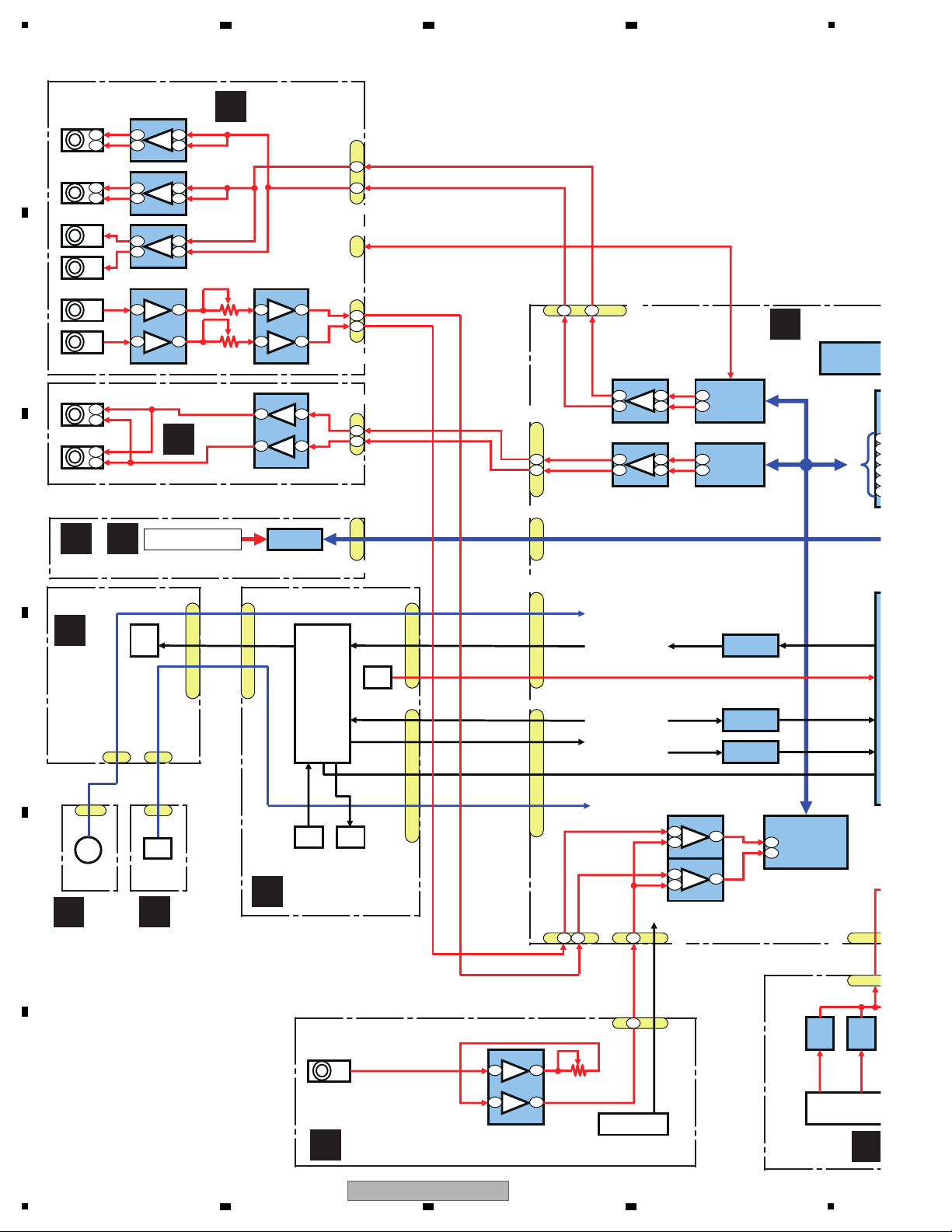
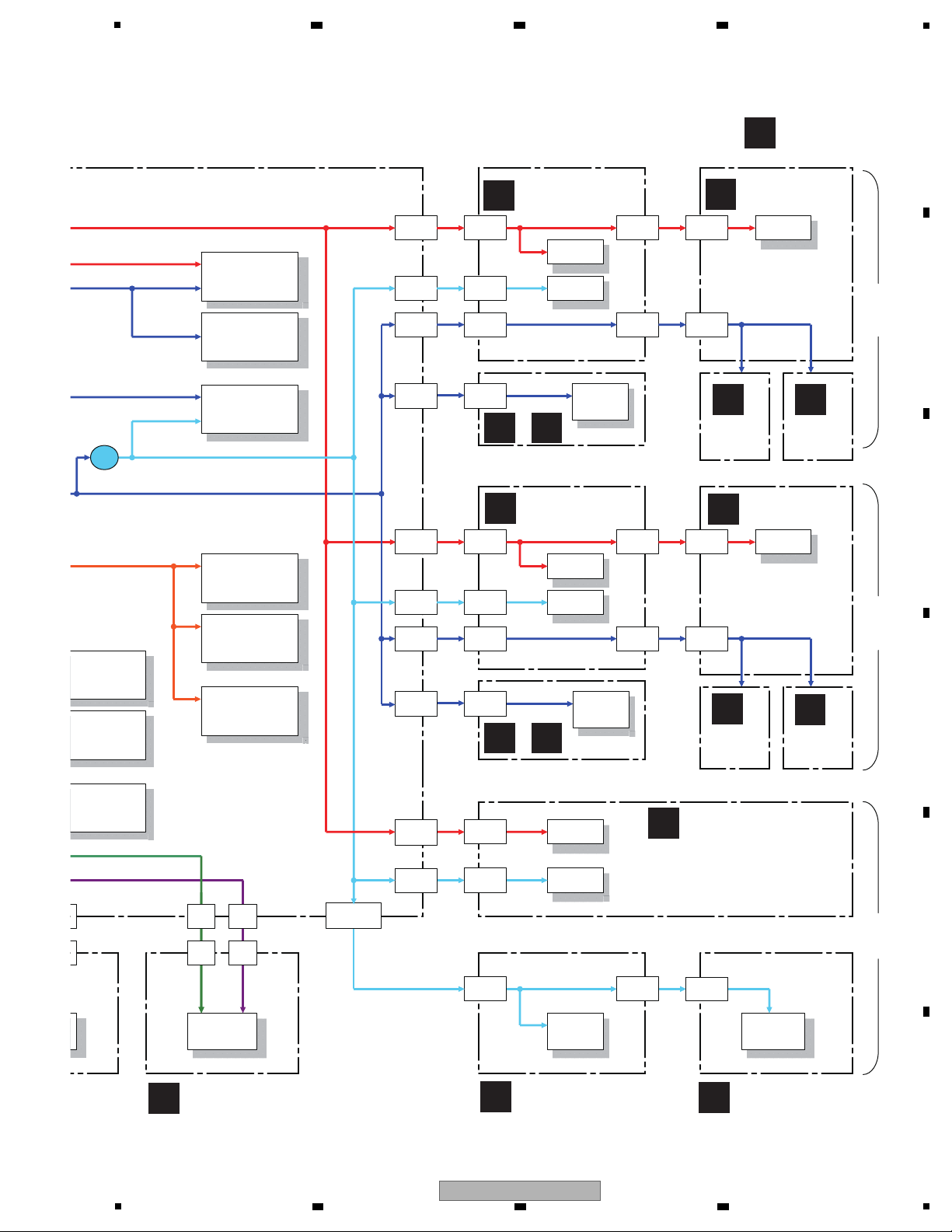
4.2 OVERALL BLOCK DIAGRAM
A
B
C
D
E
F
18
1
2 3 4
DDJ-T1
Page 19
UCOM ASSY
J
DJMB ASSY
L
CHFD ASSY
M
CRFD ASSY
G
LEDB ASSY
H
CDJ1B ASSY
E
TCHB ASSY
F
JOGB ASSY
O
USBB ASSY
USB Dp/Dn
* V+USB5 or V+ADP5
CN1004(13Pin)
ADP_DET
P_SW2_USB/PSW1_ADP
USB Dp/Dn
POWER SUPPLY
POWER SUPPLY
S2I
I2C
suBS2IS2I
)niP8(209NC
)CDC(suBIPSsuBIPS
CN2001/CN2101
I2C
CN906(20Pin)
JOG_TCH_1
Grid[7:4]
DELGOJ
]1:4[nIyeK
LED[5:0]
CN905(25Pin)
Trim / Fader
Grid[3:0]
JOG1_1/1_2
S2I
Trim
Fader
FD SATRT SW
CRFD
IC202
USB_UCOM
TUSB3200A
IC701
MAIN_UCOM
IC203
SW
IC201
EEPROM
IC303
AUX/MIC
ADC
39
38
36
44
34
35
Master Data
HP Data
MIC/AUX Data
BCL
LRCK
MCLK
41
42
SDA
SCL
5
42
43
6
IC101
DC/DC Conv.
2
1
7 8
910
10
32
IC2001/2101
CDC
Neadle Search
LED [14:12]
Grid[7:0]
Key In[12:9]
IC106
Reset IC
17
Fault_Det
Circuit
23
CN4002
CN4301
CN4202
CN4001
CN2001
JA2502JA2501
SW
Circuit
CN2501
CN3301
CN3201
CN6002
JH6001
CN6001
CN3001
CN3002
CN3003
MATRIX
Circuit
MATRIX
Circuit
MATRIX
Circuit
JOG
LED
KEY LED
Trim
KEY LED
SWICSWICSW
IC
VOL
JOG
CN1003(15Pin
CN1002(8Pin)
CN1001(25Pin)
SW
Reset
DYW1801
PEG850A8-K
C D
CDCB 1 ASSY/CDCB 2 ASSY
/
Either the CDCB 1 Assy or CDCB 2 Assy is assembled here. The CDCB 1 Assy
and CDCB 2 Assy are interchangeably used and handled similarly in their production
management.
5
5
6 7 8
DDJ-T1
6 7 8
A
B
C
D
E
F
19
Page 20
1
AUDIO AMP(MASTER)
RNB4580F
IC501
AUDIO AMP(HP)
NJM4565MD
IC305
SW AMP(AUX/MIC)
NJM2121MD x2
IC301, IC302
V+5_D
V+5_DV+5_D
POWER SLIDE SW
ASG1100
S2502
OPAMP x1
V+6 V-6
OPAMP x4
V+6
V-6
V+6 V-6
V+6
V-6
V+5
_USB
V+5
_USB
V+4R7
_STB
V+4R7
_STB
IC105
3.3V_REG
4.7V→3.3V
S-1200B33
IC102
3.3V_REG
5V→3.3V
S-1200B33
IC102
3.3V_REG
5V→3.3V
S-1200B33
V+5_U
V+3R3_
V+3R3_
V+3R3_U
V+3R3_D
V+3R3_
L707
V+USB5
V+ADP5
IC103
5V_REG
6V→5V
S-1200B50
V+5_A
IC101
D/D_CONV
5V→6V
BD9851EFV
IC101
D/D_CONV
5V→-6V
BD9851EFV
V+6
V+6
V+6
V+5_D
V-6
V-6
V+5_D
V+5_D
V+5_D
V+5_USB
V+5_USB
V+4R7_STB
USB
CABLE
AC
ADAPTER
V+6
V-6
FET RELAY SW
RTQ040P02
Q2522, Q2524
FET RELAY SW
RTQ040P02
Q2523, Q2525
V+6
V-6
A
JACB ASSY
B
UCOM ASSY
K
MICB ASSY
N
O
USBB ASSY
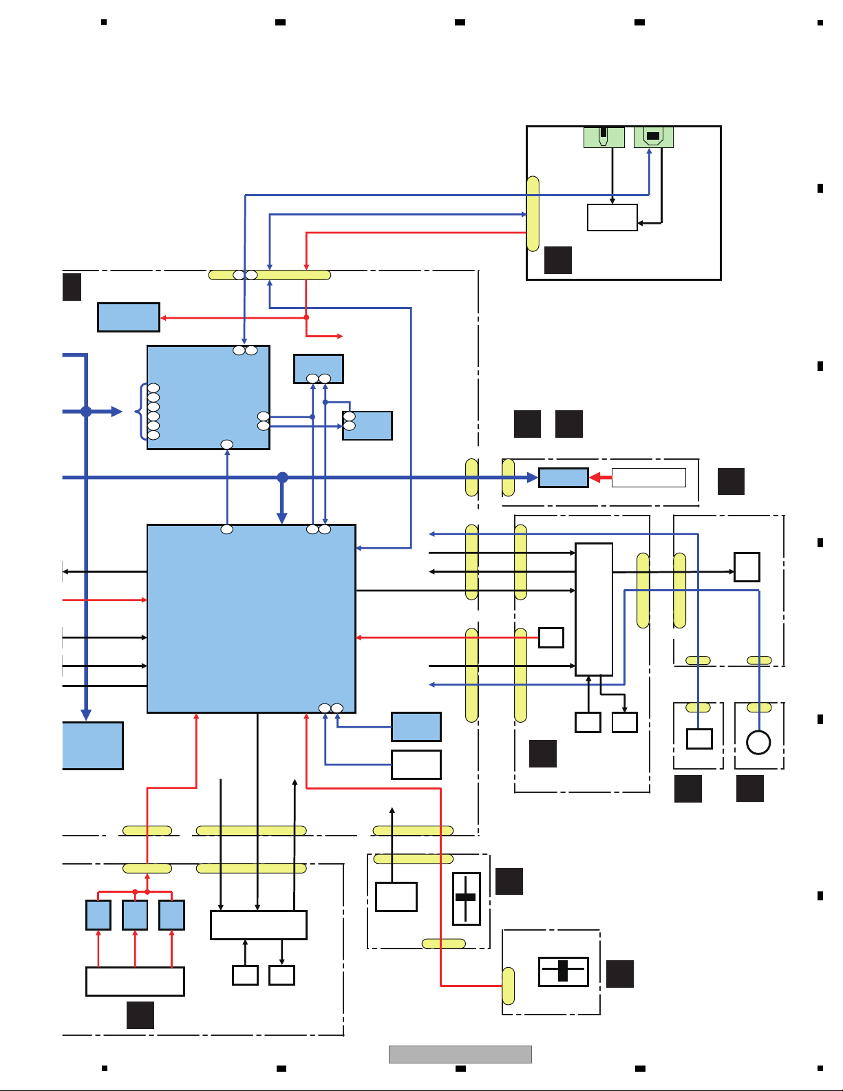
4.3 POWER BLOCK DIAGRAM
A
2 3 4
B
C
D
E
F
20
DDJ-T1
1
2 3 4
Page 21
MAIN ucom
DYW1801
PEG850A8-K
IC701
USB ucom
TUSB3200A
IC202
EEPROM
IC201
HP DAC
AK4387ET
IC304
MASTER DAC
AK4387ET
IC506
AMP(MASTER)
IC501
IC305
V+5_D
V+3R3_D
301, IC302
V+5_D
LED
NEEDL
SEARCH
VR
LED
VR
V+3R3_AD
V+5_D
V+5_D V+5_D
LED
V+3R3_AD
CH FADER
x4
CROSS
FADER
V+3R3_D
V+3R3_D V+3R3_D
V+3R3_AD
V+3R3_AD
V+3R3_D V+3R3_D
OPAMP x1
V+6
V+6
V-6
V-6
V+3R3_AD
V+5_D
V+3R3_D
V+5_D
LED
NEEDL
SEARCH
VR
V+5_D V+5_D
LED
V+3R3_D
V+3R3_D
V+3R3_D
V+3R3_D V+3R3_D
V+5_D
V+5_USB
V+3R3_USB
V+3R3_USB
V+3R3_UCO
V+3R3_D
V+3R3_AD
V+3R3_AD
L707
V+3R3_AD V+3R3_AD
V+3R3_AD V+3R3_AD
V+5_D
V+3R3_AD
V+5_A
V+3R3_D
ADC
AK5358AET
IC303
J
DJMB ASSY
L
CHFD ASSY
M
CRFD ASSY
N
HPJK ASSY
I
CDJ2B ASSY
G
LEDB ASSY
G
LEDB ASSY
H
CDJ1B ASSY
E
TCHB
ASSY
F
JOGB
ASSY
E
TCHB
ASSY
F
JOGB
ASSY
C
CDCB 1 ASSY
CDJ1
DECK
A,C
CDJ2
DECK
B,D
DJM
MIXER
C D
CDCB 1 ASSY/CDCB 2 ASSY
CDCB 1 ASSY/CDCB 2 ASSY
/
C D
/
Either the CDCB 1 Assy or CDCB 2 Assy is assembled here. The CDCB 1 Assy
and CDCB 2 Assy are interchangeably used and handled similarly in their production
management.
Either the CDCB 1 Assy or CDCB 2 Assy is assembled here. The CDCB 1 Assy
and CDCB 2 Assy are interchangeably used and handled similarly in their production
management.
5
6 7 8
A
B
C
D
E
5
6 7 8
DDJ-T1
F
21
Page 22
1
• With AC adaptor and USB connection
• With AC adaptor and w/o USB connection
• W/O AC adaptor and with USB connection (USB-bus power)
Yes
Yes
Yes
Yes
Yes
No
No
No
No
No
Note: The TUSB3200A is started up after loading
the program from the EEROM.
Note: Start the updating
program on the PC.
Normal mode
To normal main loop processing
• Power monitoring/switching
• MIC/AUX switching
• Detection of change in operating elements
• USB transmission (transmission of operating element data)
• USB reception (reception and indication of display data)
Power ON
Clock multiplying -> 32 MHz
Port initial setting
I2C serial initial setting
Checking and setting
of the power supply
Has the
power-supply status
changed?
Power failure?
Unit stopped by power
failure (All LEDs unlit)
With USB
connection?
Canceling reset of the USB
Controller and the TUSB3200A
Opening indication
Opening indication
Checking of communication
with the TUSB3200A
Has
communication been
established?
Alarm indication of abnormal
stopping of the TUSB3200A
CRC check of the main flash
CRC error?
(FLASH NG?)
Waiting for a recovery
/updating request
Interruption initial setting
Serial communication
initial setting
Timer initial setting
A/D conversion initial setting
A
A
MIC/AUX initial setting
Needle initial setting
Operation mode
judgment
Service mode
(Test mode)
JOG Load
Measurement mode
LED luminance setting
Display initial setting
Headphones level setting
5. DIAGNOSIS
5.1 POWER ON SEQUENCE
A
B
C
2 3 4
D
E
F
22
DDJ-T1
1
2 3 4
Page 23
5
[0] Prior Confirmation
[0-1] Checking in Service Mode
[0-2] Checking Internal Cables
[1] Failure in Startup (Failure in power-on, all LEDs unlit)
[1-1] Failure in the power system
In this section, causes of failure, diagnostics points, and corrective measures can be searched for according to symptoms.
Before disassembling this unit, it is recommended to infer a failure point by referring to the error code.
For the relationship of each power-supply system, see “4.3 POWER SUPPLY BLOCK DIAGRAM.”
If software of the product is updated before performing diagnostics, check that software updating has been performed
properly before proceeding to diagnostics.
If software updating has not been performed properly, update the software, following the instructions in
“8.3 UPDATING OF THE FIRMWARE.”
Contents
[0] Prior Confirmation
[1] Failure in Startup (Failure in power-on, all LEDs unlit)
[2] Display (LED indicators)
[3] Operations (Buttons/VRs/Sliders/NeedleSearch/JOG)
[4] USB connection
[5] AUDIO OUT
[6] AUDIO IN
[7] Basic Operation Check of the MAIN_UCOM
The waveform numbers and voltage confirmation-point numbers described in this section correspond to the numbers on the
schematic diagrams and PCBs.
Be sure to check the failure points, as well as checking for failure in their peripheral circuits.
In a case where the unit does not start up, even after it is turned ON, when it is powered via the AC adapter or USB-bus power connection.
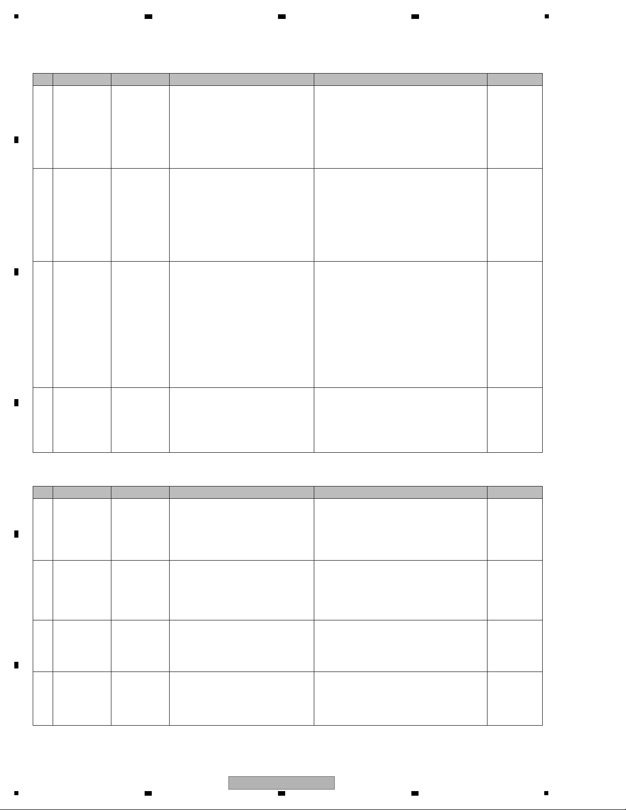
No.
Cause/Symptom
Point to be checked
Item to be checked
How to distinguish a defective point and/or corrective action
Reference
1 – Service Mode Identify a failure point.
After a failure point is identified, see the section
referenced in this manual.
6. SERVICE
MODE
No.
No.
Cause/Symptom
Point to be checked
Item to be checked
How to distinguish a defective point and/or corrective action
Reference
1
Disconnection,
breakage, or
loose connection
of internal cables
Cables
Check that all the cables are securely
connected. Check that there is no breakage
in the cables.
Securely connect a cable if it is not connected.
If a cable is broken, replace it.
Note: If an FFC cable is disconnected, be careful of
the orientation of the contacts when reconnecting it,
referring to the printed guide on the board.
4.1 OVERALL
CONNECTION
DIAGRAM
Cause/Symptom
Point to be checked
Item to be checked
How to distinguish a defective point and/or corrective action
Reference
1
Failure in the
AC adapter
USBB Assy
V+ADP5
Set the POWER switch to OFF.
Check that the voltage of the V+ADP5
power line is in the range of 4.75–5.25 V.
If the voltage is outside the range of 4.75–5.25 V,
failure in the AC adapter and its periphery may be
suspected. AC adapter (DWR1491), DC jack
(JA2501), FETs (Q2523, Q2525), Tra ( )
4.3 POWER
SUPPLY BLOCK
DIAGRAM
4.3 POWER
SUPPLY BLOCK
DIAGRAM
4.3 POWER
SUPPLY BLOCK
DIAGRAM
4.3 POWER
SUPPLY BLOCK
DIAGRAM
2
Failure in USBbus power
USBB Assy
V+USB5
Set the POWER switch to OFF.
Check that the voltage of the V+ADP5
power line is in the range of 4.75–5.25 V.
If the voltage is outside the range of 4.75–5.25 V,
failure in the USB-bus power and its periphery may
be suspected. Check the USB cable and USB
connector.
3-1
Power failure in the
MAIN_UCOM on
the UCOM Assy
UCOM Assy
MAIN_UCOM
Set the POWER switch to ON.
If V+3R3_UCOM is abnormal (2.7 V or less)
and V+4R7_STB is normal (4.2–5.0 V)
The regulator (IC105), the MAIN_UCOM (IC701),
or their peripheral circuits may be defective.
3-2
Power failure in the
USB_UCOM on
the UCOM Assy
UCOM Assy
USB_UCOM
Set the POWER switch to ON.
If V+3R3_USB is abnormal (2.7 V or less)
and the V+5_USB is normal (4.5 V–5.25 V)
The regulator (IC102), the USB_UCOM (IC202),
or their peripheral circuits may be defective.
10.17
WAVEFORMS
AC adapter
4
10.17
WAVEFORMS
Power bus power
1
6 7 8
5.2 TROUBLESHOOTING
A
B
5
DDJ-T1
6 7 8
C
D
E
F
23
Page 24
1
[1-2] Failure in the microcomputer system
4-1 Power failure 1
UCOM Assy
FAULT_DET
Check if the voltage monitoring circuit was
activated:
Turn the unit ON then check the voltages
shown below.
V+5_D:
FAULT_DET, R147 (0 Ω) :
Turn the unit ON then check the voltages shown below.
V+5_D: 2 V or less (abnormal voltage), 4.5 V or higher
(normal voltage)
FAULT_DET, R147(0
Ω
): 0 V (abnormal voltage detection),
3.3 V (normal voltage)
In a case of abnormal voltage detection, see [4–2] Power
failure
2
.
In a case of normal voltage, poor control over the
microcomputer system may be suspected.
4.3 POWER
SUPPLY BLOCK
DIAGRAM
5.3 VOLTAGE
MONITORING
4.3 POWER
SUPPLY BLOCK
5.3 VOLTAGE
MONITORING
4.1 OVERALL
CONNECTION
DIAGRAM
4.3 POWER
SUPPLY BLOCK
4.1 OVERALL
CONNECTION
DIAGRAM
4.3 POWER
SUPPLY BLOCK
5.3 VOLTAGE
MONITORING
4-2
Power failure 2
Identification of
defective Assy
UCOM Assy
FAULT_DET
CDJB
CDCB
DJMB
JACB
HPJK
MICB
Identify the Assy on which a voltage error
was generated.
Remove all cables other than the cable for
CN1004 (USBB to UCOM) from the UCOM
Assy.
Turn the unit ON then check the V+5_D
voltage.
V+5_D:
FAULT_DET, R147 (0 Ω):
Remove all cables other than the cable for CN1004 (USBB
to UCOM) from the UCOM Assy.
Turn the unit ON then check the V+5_D voltage.
V+5_D: 4.5 V or higher (normal)
FAULT_DET, R147(0 Ω): 3.3 V normal, no detection of a
voltage error)
In a case of normal voltage, see [4–3] Abnormal voltage
detection
3
.
In a case of abnormal voltage detection, see [4-4] Power
failure, UCOM Assy.
4-3
Power failure 3
Identification of
defective Assy
UCOM Assy
FAULT_DET
CDJB
CDCB
DJMB
JACB
HPJK
MICB
With all cables other than the cable for
CN1004 (USBB to UCOM) disconnected
from the UCOM_ASSY, identify the defective
Assy by connecting each connector on the
UCOM Assy one by one for voltage checks.
Identify the defective ASSY, by connecting each connector
on the UCOM Assy, as shown below, one by one for
voltage checks:
CDJ1B: CN905, CN906
CDJ2B: CN903, CN904
CDCB: CN901, CN902
DJMB: CN1001, 1002
JACB: CN302, CN501
HPJK: CN301
MICB: CN303
Repair the defective part of the defective Assy.
If further identification of defective Assys is required, see
the notes in “5.3 Voltage Monitoring” before proceeding to
further diagnostics.
4-4
Power failure 4
UCOM Assy
Identification of
defective Assy
UCOM Assy
FAULT_DET
Deactivate the voltage monitoring circuit
then check the section with improper
voltage.
The voltage monitoring circuit can be deactivated by
removing R147 (0 Ω) on the FAULT_DET.
See the notes in “5.3 Voltage Monitoring” before
proceeding to further diagnostics.
To identify the section with improper voltage, check
the voltage at each point on the UCOM Assy.
1
Power failure in
the MAIN_UCOM
UCOM Assy
Check if a voltage error was detected.
Check the power terminal of the
MAIN_UCOM (IC701).
If the detected voltage error is confirmed, check conduction
between the power supply and GND.
Check the power line and the parts, such as coils (beads),
resistors, and capacitors.
If no problem was found with the parts, power line, and
conduction between the power supply and GND, the
MAIN_UCOM
(IC701) may be defective.
Abnormal
Voltage Detection
2
MAIN_UCOM
Reset circuit
error
UCOM Assy
Check the Reset terminal (Pin 17) of the
MAIN_UCOM (IC701). (High/Low)
In normal operation, the voltage of the Reset terminal
(Pin 17) is high.
If the voltage of the Reset terminal is low, check the power
line, resistors, capacitors, and the Reset IC (IC106).
If the voltage level remains low after the Reset IC (IC106)
is replaced, the
MAIN_UCOM
(IC701) may be defective.
3
MAIN_UCOM
X'tal error
UCOM Assy
Check the oscillation waveforms of the
X'tal (X701).
Check the waveforms of the X'tal (X701).
If an error is found, check the power line, resistors, and
capacitors.
If the waveform remains abnormal after the X'tal (X701) is
replaced, the
MAIN_UCOM
(IC701) may be defective.
4
MAIN_UCOM
startup error
UCOM Assy
After startup, check the lighting statuses of
the LEDs.
(For example, although some of the LEDs
light properly, the unit is not started up
properly.)
Refer to “[4] Error Indications” in the 6. Service Mode.
If there is no corresponding error indication, reload the
program via USB.
If the normal status is not recovered after all above steps
are performed, the
MAIN_UCOM
(IC701) may be
defective.
6. Service Mode
[4]
Error Indications
No.
Cause/Symptom
Point to be checked
Item to be checked
How to distinguish a defective point and/or corrective action
Reference
No.
Cause/Symptom
Point to be checked
Item to be checked
How to distinguish a defective point and/or corrective action
Reference
10.17
WAVEFORMS
Abnormal voltage
detection
k, p
10.17
WAVEFORMS
Abnormal voltage
detection
k, p
10.17
WAVEFORMS
MAIN UCOM
start up
10.17
WAVEFORMS
MAIN UCOM
start up
i
10.17
WAVEFORMS
MAIN UCOM
start up
j
A
2 3 4
B
C
D
E
F
24
1
DDJ-T1
2 3 4
Page 25
5
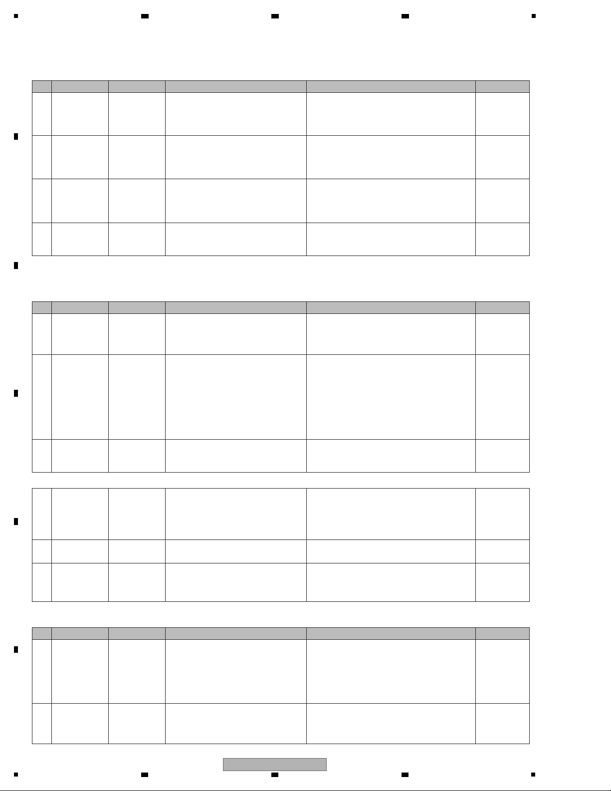
[2] Display (LED indicators)
[2-1] Any one of the LEDs does not light.
[3] Operations (Buttons/VRs/Sliders/NeedleSearch/JOG)
[3-1] The push buttons are disabled.
5
Power failure in
the USB_UCOM
UCOM Assy
Check if a voltage error was detected.
Check the power terminal of the
USB_UCOM (IC202).
If the detected voltage error is confirmed, check conduction
between the power supply and GND.
Check the power line and the parts, such as coils (beads),
resistors, and capacitors.
If no problem was found with the parts, power line, and
conduction between the power supply and GND, the USB_
UCOM (IC202) may be defective.
Abnormal
Voltage Detection
6
USB
_UCOM
Reset circuit
error
UCOM Assy
Check the Reset terminal (Pin 10) of the
USB_UCOM (IC202). (High/Low)
In normal operation, the voltage of the Reset terminal
(Pin 10) is high.
If the voltage level at the Reset terminal is low, check for
abnormal voltage detection, and check the power line,
resistors, and capacitors. If no problem was found with the
above circuit, parts, and power line, and if the voltage level
is low, the USB_UCOM (IC202) or the MAIN_UCOM
(IC701) may be defective.
Abnormal
Voltage Detection
7
USB
_UCOM
X'tal error
UCOM Assy
Check the oscillation waveforms of the
X'tal (X201).
If an error is found, check the power line, resistors, and
capacitors.
If the waveform remains abnormal after the X'tal (X201) is
replaced, the USB_UCOM (IC202) may be defective.
8
USB
_UCOM
I2C communication error
UCOM Assy
Check the I2C communication waveforms of the
EEPROM (IC201) immediately after startup.
Data of the EEPROM (IC201) are loaded only during
startup.
If an error is generated, check the power supply to the
EEPROM, resistors, capacitors, and SW IC (IC203) on the
communication line.
If no problem is found with the power supply, communication line, and parts, the EEPROM (IC201) or USB_UCOM
(IC202) may be defective.
9
EEPROM error
UCOM Assy Reload the program via USB.
If no problem is found with the communication waveform in
[8] above, reload the program via USB.
If reloading is successfully performed, the USB_UCOM
(IC202) may be defective.
If reloading fails, the EEPROM (IC201) may be defective.
1 Defective LED LERelated point
Check the connections of the LED then
check the forward voltage (approx. 2.2 V)
between both ends of the LED.
If the forward voltage is abnormal, the LED may be
defective.
LED waveform
10.SCHEMATIC
DIAGRAM
[2-2] Several LEDs do not light.
1 Signal errors
UCOM Assy
CDJ1B
CDJ2B
DJMB
Check for any loose connections between
the MAIN_UCOM (IC701) and the LEDs.
Check also that the control signal for the
LEDs is output.
If the control signal is not output, check the
mounting status of the MAIN_UCOM (IC701).
If it is properly mounted, then the IC701 itself may
be defective.
Basic Operation
Check of the
MAIN_UCOM
Basic Operation
Check of the
MAIN_UCOM
2 Defective LEDs Related point
Check the forward voltage (approx. 2.2 V)
between both ends of the LEDs.
If the forward voltage is abnormal, the LEDs may be
defective.
LED waveform
10.SCHEMATIC
DIAGRAM
3
Defective
transistors
Related point Check the transistors. The transistors may be defective.
10.SCHEMATIC
DIAGRAM
Operation of all buttons, variable controls, and the JOG dial can be confirmed in Service mode.
1
Loose connection
or defective
switches
Related point
Check for any loose connections on the
signal line from the switch to GRID_IC
(IC702), KEY_BUFFER (IC1101, 1102),
and main microcomputer (IC701).
If other SWs connected to the same signal line
function properly and if the connections are properly
made, the SW may be defective.
Each Signal
Levels
2
Defective MAIN_
UCOM (IC701)
UCOM Assy
If the symptom persists after the above
corrections.
Go to [7-1] Basic Operation Check of the
Microcomputer.
No.
Cause/Symptom
Point to be checked
Item to be checked
How to distinguish a defective point and/or corrective action
Reference
No.
Cause/Symptom
Point to be checked
Item to be checked
How to distinguish a defective point and/or corrective action
Reference
No.
Cause/Symptom
Point to be checked
Item to be checked
How to distinguish a defective point and/or corrective action
Reference
No.
Cause/Symptom
Point to be checked
Item to be checked
How to distinguish a defective point and/or corrective action
Reference
10.17
WAVEFORMS
USB UCOM
start up
10.17
WAVEFORMS
USB UCOM
start up
c
10.17
WAVEFORMS
USB UCOM
start up
d
10.17
WAVEFORMS
I2C USB UCOM
EEPROM
8.4 COPYING THE
PROGRAM FOR THE
USB CONTROLLER
6 7 8
A
B
C
5
DDJ-T1
6 7 8
D
E
F
25
Page 26
1
[3-2] Rotary selector not controllable
1
Defective
AUTO_LOOP
of the CDJ1
CDJ1 Assy
Check that the signal lines (L_ENC1_1/
L_ENC1_2) are normal during rotation of
the rotary selector.
L_ENC1_1: CN3002-1 pin
L_ENC1_2: CN3002-2 pin
If the signals are not normal, check the connections of the
signal lines. If the connections are properly made, the
rotary selector (S3030) may be defective. Replace it.
Each Signal
Levels
2
Defective
AUTO_LOOP
of the CDJ2
CDJ2 Assy
Check that the signal lines (L_ENC2_1/
L_ENC2_2) are normal during rotation of
the rotary selector.
L_ENC2_1: CN3502-6 pin
L_ENC2_2: CN3502-5 pin
Check that the signal lines (CUR_ENC1/
CUR_ENC2) are normal during rotation of
the rotary selector.
CUR_ENC1: CN4002-21 pin
CUR_ENC2: CN4002-22 pin
If the signals are not normal, check the connections of the
signal lines. If the connections are properly made, the
rotary selector (S3527) may be defective. Replace it.
Each Signal
Levels
3
Defective
DJM
BROWSE
DJMB Assy
If the signals are not normal, check the connections of the
signal lines. If the connections are properly made, the
rotary selector (S4027) may be defective. Replace it.
Each Signal
Levels
4
Defective
MAIN_UCOM
(IC701)
UCOM Assy
If the symptom persists after the above
corrections.
Check the mounting status of the MAIN_UCOM (IC701).
If it is properly mounted, then the IC701 itself
may be defective.
Basic Operation
Check of the
MAIN_UCOM
Basic Operation
Check of the
MAIN_UCOM
Basic Operation
Check of the
MAIN_UCOM
[3-3] VRs or sliders not controllable
The variable controls on the CDJ1 and CDJ2 Assys or the sliders on the CHFD and CRFD ASSYs are not controllable.
VRs on the DJMB ASSY not controllable.
1
Loose
connection
CDJ1/CDJ2 Assy
CHFD Assy
CRFD Assy
Check for any loose connections on the
signal line from the MAIN_UCOM (IC701)
to each variable control or slider.
If any connection on the signal line is improper, resolder
the parts.
—
2
Defective
sliders or VRs
CDJ1/CDJ2 Assy
CHFD Assy
CRFD Assy
VRs: Check the signal level.
Tempo slider: Check the levels of the
ADCT and ADIN signals.
CHFD, CRFD: Check the signal level.
VRs: If the voltage of the signal from a VR (Pin 2) does not
change between 3.3 V and 0 V, that VR may be defective.
Tempo slider: If the value of the voltage of the ADCT signal
(Pin 4) is other than 1.65 V, or if the voltage of the ADIN
signal (Pin 2) does not change between 3.3 V and 0 V, the
tempo slider may be defective.
CHFD, CRFD: If the voltage of the signal from the CHFD
or CRFD (Pin 2) does not change between 3.3 V and 0 V,
the slider may be defective.
Each Signal
Levels
Each Signal
Levels
3
Defective
MAIN_UCOM
(IC701)
UCOM Assy
If the symptom persists after the above
corrections.
Check the mounting status of the MAIN_UCOM (IC701).
If it is properly mounted, then the IC701 itself
may be defective.
4
Loose
connection
DJMB Assy
Check for any loose connections on the signal
line from each VR to Analog SW_IC (IC4001,
IC4002, IC4003) and the main microcomputer
(IC701).
Signal line: AD_0–4, AD_SW_A, AD_SW_B
If any connection on the signal line is improper, resolder
the parts.
—
5 Defective VRs DJMB Assy VRs: Check the signal level.
VRs: If the voltage of the signal from a VR (Pin 2) does not
change between 3.3 V and 0 V, that VR may be defective.
6
Defective
MAIN_UCOM
(IC701)
UCOM Assy
If the symptom persists after the above
corrections.
Check the mounting statuses of the MAIN_UCOM (IC701)
and the Analog SW_IC (IC4001, IC4002, IC4003).
If they are properly mounted, then the IC701, IC4001,
IC4002, or IC4003 may be defective.
[3-4] NeedleSearch error
1
CDC IC Error/
Needlepad disabled (Incl. steps 4
and 5 of [4] Error
indications in the
6. Service Mode)
UCOM/CDCB
Assy
Check the communication waveform
between the needlepad and the MAIN_
UCOM (IC701).
If the waveform is not proper, check the communication
line, resistors, and capacitors.
Check also that the cables between the boards and their
connections are proper.
If the normal status is not recovered after all above steps
are performed, the CDC IC or the MAIN_UCOM (IC701)
may be defective.
2
Only some of the
commands from
the needlepad are
recognized.
UCOM/CDCB
Assy
Check that no foreign matter is between
the Needlepad board and the cabinet.
If the Needlepad operates improperly although there is no
foreign matter between the Needlepad board and the
cabinet, check [2] above.
No.
Cause/Symptom
Point to be checked
Item to be checked
How to distinguish a defective point and/or corrective action
Reference
No.
Cause/Symptom
Point to be checked
Item to be checked
How to distinguish a defective point and/or corrective action
Reference
No.
Cause/Symptom
Point to be checked
Item to be checked
How to distinguish a defective point and/or corrective action
Reference
10.17
WAVEFORMS
CDC IC control 1/2
A
B
2 3 4
C
D
E
F
26
1
2 3 4
DDJ-T1
Page 27
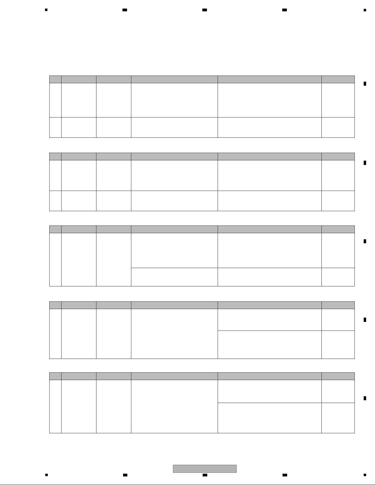
5
[3-5] Abnormalities regarding the JOG dial
After the JOG Assy is disassembled then reassembled, be sure to check that the load value for the JOG dial is within the specified range.
Refer to the "8.5 JOG DIAL ROTATION LOAD ADJUSTMENT".)
Turning of the JOG dial is not detected.
1
Defective JOGB
photo interrupter
UCOM Assy
CDJ1ssy
/CDJ2 Assy
LEDB Assy
JOGB Assy
Check the waveforms on the JOG1_1,
JOG1_2, JOG2_1, and JOG2_2 signal lines.
JOG1_1: CN905-2 pin
JOG1_2: CN905-3 pin
JOG2_1: CN905-24 pin
JOG2_2: CN905-23 pin
If any waveform cannot be recognized, connection
of that signal line may be loose or the photo
interrupter (PC3201) may be defective.
10.17
WAVEFORMS
2
Defective
MAIN_UCOM
(IC701)
UCOM Assy
If the symptom persists after the above
corrections.
Check the mounting status of the MAIN_UCOM
(IC701). If it is properly mounted, then the IC701
itself may be defective.
Basic Operation
Check of the
MAIN_UCOM
Pressing on the JOG dial cannot be detected.
3
Defective
TCHB photo
interrupter
UCOM Assy
CDJ1 Assy
/CDJ2 Assy
TCHB Assy
JOGB Assy
Check the signal level of the JOG_TCH1/2
(Pins 46/47 of IC701) when the JOG dial is
pressed.
If the signal level of the JOG_TCH1/2 (Pins 46/47 of
IC701) does not become L when the dial is pressed
and H when the dial is released (not pressed,) loose
connection of the signal line or a defective photo
interrupter (IC3301) may be suspected.
Each Signal
Levels
4
Defective
MAIN_UCOM
(IC701)
UCOM Assy
If the symptom persists after the above
corrections.
Check the mounting status of the MAIN_UCOM
(IC701) and SW IC (IC702). If they are properly
mounted, then the IC701 or IC702 may be defective.
—
Noise is heard when the JOG dial is turned.
5
Defective gear
Defective JOG
DIAL B
JOG Assy
There may be any scratches on the gear
or some foreign matter between the gears.
If there are any scratches, replace the scratched
gear with a new one.
If there is any foreign matter, remove it then replace
the gears with new ones.
Gears to be replaced: Load gear, Encoder gear,
JOG shaft
—
There may be any scratches or some
foreign matter on the JOG DIAL B or the
Roller B Assy.
If there are any scratches, replace the scratched
gear with a new one.
If any foreign matter is attached, remove it.
—
The JOG dial turns too freely. (The load value for the JOG dial is outside the specified range.)
6
Improper
adjustment or
assembly of the
JOG dial
JOG Assy
Check that the load value for the JOG dial
is within the specified range, referring to
“Measuring method” in “8.5 JOG Dial
Rotation Load Adjustment.”
If it is outside the specified range, adjust the position
of the Adjust Plate to change the load value for the
JOG dial, referring to “Load adjustment method” in
“8.5 JOG Dial Rotation Load Adjustment.”
8.5 JOG Dial
Rotation Load
Adjustment.
8.5 JOG Dial
Rotation Load
Adjustment.
8.5 JOG Dial
Rotation Load
Adjustment.
8.5 JOG Dial
Rotation Load
Adjustment.
During the above adjustment, if the upper-limit
adjustment position of the Adjust Plate is reached,
oil may have been spattered on the Adjust Plate.
Replace the washer, load gear, and cam plate with
new ones, then reassemble.
Resistance to turning the JOG dial is too strong. (The load value for the JOG dial is outside the specified range.
7
Improper
adjustment of
the JOG dial or
defective washer,
gear, or cam plate
JOG Assy
Check that the load value for the JOG dial
is within the specified range, referring to
“Measuring method” in “8.5 JOG Dial
Rotation Load Adjustment.”
If it is outside the specified range, adjust the position
of the Adjust Plate to change the load value for the
JOG dial, referring to “Load adjustment method” in
“8.5 JOG Dial Rotation Load Adjustment.”
During the above adjustment, if the lower-limit
adjustment position of the Adjust Plate is reached,
shavings from the worn-out washer may have
increased the friction. Replace the washer, load gear,
and cam plate with new ones, then reassemble.
No.
Cause/Symptom
Point to be checked
Item to be checked
How to distinguish a defective point and/or corrective action
Reference
No.
Cause/Symptom
Point to be checked
Item to be checked
How to distinguish a defective point and/or corrective action
Reference
No.
Cause/Symptom
Point to be checked
Item to be checked
How to distinguish a defective point and/or corrective action
Reference
No.
Cause/Symptom
Point to be checked
Item to be checked
How to distinguish a defective point and/or corrective action
Reference
No.
Cause/Symptom
Point to be checked
Item to be checked
How to distinguish a defective point and/or corrective action
Reference
10.17
WAVEFORMS
JOG rotation
operation W
6 7 8
A
B
C
D
E
F
DDJ-T1
5
6 7 8
27
Page 28
1
[4] USB connection
[4-1] The unit cannot be recognized by the PC when connected to the PC via USB connection.
Check the following, with a Windows/MAC PC connected via the USB port of the unit, using the supplied USB cable:
1 Failure in startup
UCOM/USBB
Assy
Check the lighting statuses of the LEDs
during startup.
If no LED lights, see [1] Failure in Startup.
[1] Failure in
Startup
2
Defective
USB_UCOM
UCOM/USBB
Assy
Check the communication waveforms of
the USB DP/DN lines.
If the unit is connected to a PC via the USB cable,
communication will be performed through the USB
DP/DN lines.
If communication cannot be performed, check the
USB cable, connectors, internal cables, resistors,
capacitors, and filters.
If nothing is wrong with them, check the items listed
in “Failure in the microcomputer system” and “USB
UCOM startup error.”
Failure in the
microcomputer
system
USB_UCOM
startup error
[5] AUDIO OUT
[5-1] No signal is output from the MASTER connectors
1 — MASTER1/2
Identify the connector(s) that do(es) not
output signals.
Check if no signal is output from both MASTER 1 and 2 or
either of them.
• If neither MASTER 1 nor 2 connector outputs, go to [2].
• If only the MASTER 1 connector does not output, go to [7].
• If only the MASTER 2 connector does not output, go to [8].
—
2 — UCOM Assy
Check the audio signal, using Pins 5 and 9
of the CN501 on the UCOM Assy.
If no audio signal is output, loose connection or
defective parts in the UCOM Assy may be suspected.
• If an audio signal is output, go to [7] or [8].
• If an audio signal is not output, go to [3].
10.4 UCOM
ASSY (3/6)
10.4 UCOM
ASSY (3/6)
10.4 UCOM
ASSY (3/6)
10.4 UCOM
ASSY (3/6)
10.4 UCOM
ASSY (3/6)
10.1 JACB ASSY
10.1 JACB ASSY
3 — UCOM Assy
Check that an audio signal is output from
DAC (IC506).
• If an audio signal is output, go to [5].
• If an audio signal is not output, go to [4].
4 UCOM Assy
Check the digital input signals to DAC (IC506).
• DAC_RST
• MCLK
• BCLK
• LRCK
• MASTER_DATA
If any of the signals is not input, check the soldering
status of DAC (IC506).
If the level of DAC_RST is L, check the connections
of the MAIN_UCOM (IC701). If nothing is wrong with
the connec-tions, then the MAIN_UCOM (IC701)
itself may be defective.
If other signals are not input, check the connections
of the USB_UCOM (IC202). If nothing is wrong with
the connections, then the USB_UCOM (IC202) itself
may be defective.
5 UCOM Assy
Check that the MUTE signal level is L
(muting canceled).
If the MUTE signal level is L (muting canceled,)
check the connections between the DAC and CN501.
If nothing is wrong with the connections, soldering of
the OP amp (IC501) or the OP amp itself may be
defective.
If the MUTE signal level is H, go to [6].
6 UCOM Assy
Check that the A_MUTE signal level is L
(muting canceled).
If the A_MUTE signal level is L (muting canceled,)
check that the signal logics for Q583/Q505/Q506/
Q581/Q582 are the same as those described in the
schematic diagrams. If any of the signal logic is not
the same, repair the defective point.
If the A_MUTE signal level is not L (muting canceled),
the soldering status of the MAIN_UCOM (IC701) or
the MAIN_UCOM itself may be defective.
7 JACB Assy
Identify the point where the audio signal is
interrupted on the line from CN4401 to the
jacks (JA4402/JA4404).
If the audio signal is interrupted at the periphery of
the OP amp (IC4403/IC4405), check the soldering
status of the OP amp. If it is properly soldered, then
the OP amp itself may be defective.
8 JACB Assy
Identify the point where the audio signal is
interrupted on the line from CN4401 to the
jacks (JA4403).
If the audio signal is interrupted at the periphery of
the OP amp (IC4404), check the soldering
status of the OP amp. If it is properly soldered, then
the OP amp itself may be defective.
No.
Cause/Symptom
Point to be checked
Item to be checked
How to distinguish a defective point and/or corrective action
Reference
No.
Cause/Symptom
Point to be checked
Item to be checked
How to distinguish a defective point and/or corrective action
Reference
Loose connection
/defective parts
Loose connection
/defective parts
Loose connection
/defective parts
Loose connection
/defective parts
Loose connection
/defective parts
10.17
WAVEFORMS
USB DP/DN (1),(2)
t, u
10.17
WAVEFORMS
DAC reset cancel
DAC I2S (1),(2)
10.17
WAVEFORMS
Output MUTE cancel
#
10.17
WAVEFORMS
Output MUTE cancel
"
A
2 3 4
B
C
D
E
F
28
1
2 3 4
DDJ-T1
Page 29
5
[5-2] No signal is output from the HP connector
1 — UCOM Assy
Check the audio signal, using Pins 3 and 5
of the CN301 on the UCOM Assy.
If no audio signal is output, loose connection or defective parts in the UCOM Assy may be suspected.
• If an audio signal is output, go to [5].
• If an audio signal is not output, go to [2].
2 — UCOM Assy
Check that the audio signal is output from
DAC (IC304).
• If an audio signal is output, go to [4].
• If an audio signal is not output, go to [3].
3 UCOM Assy
Check the digital input signals to DAC
(IC304).
• DAC_RST (IC304-5 pin)
• HP_DATA (IC304-3 pin)
For DAC_RST, check the soldering status of DAC
(IC304). If the HP_DATA signal is not input, check
the connections of the USB_UCOM (IC202).
If nothing is wrong with the connections, then the
USB_UCOM (IC202) itself may be defective.
4 UCOM Assy
Identify the point where the audio signal is
interrupted on the line from DAC (IC304) to
the CN301.
If the audio signal is interrupted at the periphery of
the OP amp (IC305), soldering of the OP amp or the
OP amp itself may be defective.
5 HPJK Assy
Identify the point where the audio signal is
interrupted on the line from CN4801 to
the JA4801.
If the audio signal is interrupted at the periphery of
the OP amp (IC4801), soldering of the OP amp or the
OP amp itself may be defective.
[6] AUDIO IN
[6-1] The input signal to AUX/MIC is not output.
0
Prior confirmation
of input
TRAKTOR setting
AC adaptor connection
AUX/MIC
Check that the TRAKTOR input setting is properly
made. Check that the AC adaptor is properly
connected. (When USB-bus power is used, the
signal input to AUX/MIC is not available.)
Operating
Instructions
10.3 UCOM
ASSY (2/6)
10.3 UCOM
ASSY (2/6)
10.3 UCOM
ASSY (2/6)
10.3 UCOM
ASSY (2/6)
10.1 JACB
ASSY
10.13 MICB
ASSY
10.3 UCOM
ASSY (2/6)
10.3 UCOM
ASSY (2/6)
10.2 UCOM
ASSY (1/6)
10.4 UCOM
ASSY (3/6)
10.3 UCOM
ASSY (2/6)
10.3 UCOM
ASSY (2/6)
10.3 UCOM
ASSY (2/6)
10.3 UCOM
ASSY (2/6)
10.14 HPJK
ASSY
1 — AUX/MIC
Identify the connector(s) whose input
signal(s) is(are) not output.
Check if the signal can be input neither AUX nor MIC
or either of them.
• If neither of them can receive signals, go to [2].
• If only the AUX connector cannot receive signals, go to [7].
• If only the MIC connector cannot receive signals, go to [8].
2
Loose connection
/defective parts
Loose connection
/defective parts
Loose connection
/defective parts
Loose connection
/defective parts
Loose connection
/defective parts
Loose connection
/defective parts
Loose connection
/defective parts
Loose connection
/defective parts
Loose connection
/defective parts
Loose connection
/defective parts
Loose connection
/defective parts
Loose connection
/defective parts
UCOM Assy
Check that the audio signal is input to the
ADC (IC303).
• If an audio signal is output, go to [3].
• If an audio signal is not output, go to [5].
3 UCOM Assy
Check the digital input signals to ADC
(IC303).
• ADC_RST (IC303-13 pin)
• MIC_AUX_DATA (IC303-1,2 pins)
If the level of ADC_RST is L, check the connections
of the MAIN_UCOM (IC701). If nothing is wrong with
the connections, then the MAIN_UCOM (IC701)
itself may be defective.
If the MIC_AUX_DATA signal is not input, check the
connections. If nothing is wrong with the connections,
then the ADC (IC303) may be defective.
4 UCOM Assy
Check the connections of the USB_UCOM
(IC202).
If nothing is wrong with the connections, then soldering of the USB_UCOM (IC202) or the USB_UCOM
itself may be defective.
5 UCOM Assy
Check that the AIN_MUTE signal level is L
(muting canceled).
If it is not L (muting canceled,) check Q509. If the
symptom persists, soldering of the MAIN_UCOM
(IC701) or the MAIN_UCOM itself is defective.
6 UCOM Assy
Check the connections between the SW AMP
(IC301/IC302) and ADC (IC303) of the MAIN.
If the connections are properly made, soldering of the
SW AMP (IC301/IC302) or the SW AMP itself is defective.
7 JACB Assy
Check that an audio signal is input to Pins 4
and 6 of the CN4402.
If a signal is input, go to [9].
If a signal is not input, identify the point where the audio
signal is interrupted on the line from the AUX terminal
(JA4401) to the CN4402.
If an audio signal is interrupted at the periphery of the
OP amp (IC4401/IC4402), soldering of the OP amp or
the OP amp itself may be defective.
8 MICB Assy
Check that an audio signal is input to Pin 4
of the CN4601.
If a signal is input, go to [9].
If a signal is not input, identify the point where the audio
signal is interrupted on the line from the MIC terminal
(JA4601) to the CN4601.
If an audio signal is interrupted at the periphery of the
OP amp (IC4601), soldering of the OP amp or the OP
amp itself may be defective.
9 UCOM Assy
Check the connections between CN302
(AUX)/CN303 (MIC) and SW AMP (IC301
/IC302).
If the connection is improperly made, correct it.
10 UCOM Assy
Check AUX_MIC_SEL.
• When AUX is selected: “H”
• When MIC is selected: “L”
If it is not, check Q301. If the symptom persists,
soldering of the MAIN_UCOM (IC701) or the MAIN_
UCOM itself is defective.
No.
Cause/Symptom
Point to be checked
Item to be checked
How to distinguish a defective point and/or corrective action
Reference
No.
Cause/Symptom
Point to be checked
Item to be checked
How to distinguish a defective point and/or corrective action
Reference
10.17
WAVEFORMS
ADC reset cncel
Z
ADC I2S(1),(2),(3)
,
10.17 WAVEFORMS
Input MUTE cancel
$
10.17 WAVEFORMS
MIC,AUX No.
)
6 7 8
A
B
5
6 7 8
DDJ-T1
C
D
E
F
29
Page 30
1
[7] Basic Operation Check of the MAIN_UCOM
Note: First, check if the voltage at each section is OK.
1
GRID Operation
Check
(No operation
with keys, VRs,
sliders, or LEDs)
UCOM Assy
Check the power to and the input/output
waveforms of the GRID IC (IC702)
If the waveform is not proper, check the GRID line
and the parts, such as resistors and capacitors.
If the output waveform is not proper, check item [2].
If nothing is wrong with the parts, the GRID IC
(IC702) or the MAIN_UCOM (IC701) may be
defective.
2
UCOM Assy
Assy
corresponding
to each key
Check the output waveform of the GRID IC
(IC702), with the FFC cable of the UCOM
Assy disconnected.
If the waveform returns to normal, the PCB Assy that
is connected with the UCOM Assy via the FFC cable
may be defective.
If the waveform does not return to normal, the GRID
IC (IC702) may be defective.
3
KEY Buffer
operation (key
input disabled)
UCOM Assy
Check the power supply to the KEY Buffer
ICs (IC1101 and 1102) and the input/output
waveforms when a key is pressed.
If the input waveform appears but the output
waveform does not when a corresponding key is
pressed, the KEY Buffer ICs (IC1101 and 1102) may
be defective.
If the input waveform does not appear when a
corresponding key is pressed, check item [4].
No operation
button is
effective.
4
UCOM Assy
Assy
corresponding
to each key
Check the connection of the FFC cable.
Check also the key input circuit of the PCB
Assy connected.
If the key input circuit of the board connected is
normal, the KEY Buffer ICs (IC1101 and 1102) may
be defective.
10.7 UCOM
ASSY (6/6)
No.
Cause/Symptom
Point to be checked
Item to be checked
How to distinguish a defective point and/or corrective action
Reference
10.17
WAVEFORMS
GRID control 1,
GRID control 2
10.17
WAVEFORMS
GRID control 1,
GRID control 2
10.17
WAVEFORMS
KEY operation 1,2
A
2 3 4
B
C
D
E
F
30
DDJ-T1
1
2 3 4
Page 31

5
The MAIN_UCOM of this unit always monitors for power failure of the unit and will shut the unit off immediately after
an error is detected.
Content to be monitored
Any power failure generated inside the Power block on the UCOM_ASSY, such as voltage drop and voltage rise.
Power to be monitored: V+5_D, V+5_A, V+6, V-6, V+3R3_D, V+3R3_UCOM
Microcomputer Detection terminal and its terminal voltage
TP103 (F-DET, TP terminal) or IC701 (MAIN_UCOM) 23-pin FAULT_DET terminal
Normal: 3.3 V
Abnormal: 0 V
Timing of monitoring start
400 msec after the unit is turned ON
Timing upon judgment as a failure
50 msec after an error is detected
LED indication when an error is generated
All LEDs are unlit after an error is generated.
With other models, the Standby LED flashes to notify of a power failure. However, this does not apply to this model,
because a Standby LED is not provided with it.
Restoration method
After the unit shuts itself off because of an error, after completing diagnosis, disconnect the AC adapter and USB cable
and wait at least 1 minute before turning the unit back on.
Diagnostic procedure
1 Disconnect the AC adapter and USB cable.
2 Remove R147 from the UCOM Assy. Note: This step will disable power monitoring.
3 Reconnect the AC adapter and USB cable.
4 As the unit is turned on in a normal way, check each voltage in this state.
Note: Because power will be forcibly supplied even if any voltage is abnormal, if abnormal voltage continues, the defective
point may produce heat, which may be dangerous. Therefore, during diagnosis, be sure to disconnect the AC
adapter and USB cable several seconds after they are connected so that forcible powering will not continue.
5 If the voltage of any power IC is abnormal, the circuit that uses that power or the power IC itself may be defective.
6 Repair the defective part then check that the voltage of the repaired part becomes normal.
7 Return R147 to its original position on the UCOM Assy.
Note: This step will enable power monitoring.
6 7 8
5.3 VOLTAGE MONITORING
A
B
C
D
E
F
DDJ-T1
5
6 7 8
31
Page 32

1
[Preparations]
Make preparations, as indicated below, on the PC before performing an operation check of the DDJ-T1.
1. Installation of TRAKTOR PIONEER DDJ-T1 EDITION (for Windows)
2. Installation of the Driver Software (for Windows)
3. Standard use setting of TRAKTOR
4. Import tracks to TRAKTOR.
Use TRAKTOR in Demo mode ("Run Demo").
A PC with the following specifications is required for operation of TRAKTOR:
Operation check of the volume controls, faders, and rotary encoders must be performed with the TRAKTOR software.
The TRAKTOR software is also required for checking the analog audio input/output.
For operation check using the TRAKTOR software, proceed as follows:
1. Installation of TRAKTOR PIONEER DDJ-T1 EDITION (for Windows)
The compressed installer file for "TRAKTOR PIONEER DDJ-T1 EDITION" will be posted on the Niis Web site:
Folder names: Traktor Installer Win.zip (for Windows) and Traktor Installer Mac.mpkg.zip (for Macintosh)
Download the necessary zip folder from Niis then unzip it.
[Installation Procedures]
Double-click on "Traktor Setup PC.exe" (unzipped file) to display the Setup screen.
Click on [Next] to proceed.
After the Setup screen is started, click on "Next" to proceed.
When the "License Agreement" screen is displayed, check the "I accept . . ." checkbox then click on "Next."
On other screens, basically proceed to the next screen by clicking on "Next" without doing anything.
When installation is finished, click on "Finish."
The three icons are displayed on the desktop.
This completes installation of TRAKTOR PIONEER DDJ-T1 EDITION.
2. Installation of the Driver Software (for Windows)
The driver software for this product is posted on the Pioneer Web site. Download it, as required.
This driver software is an Audio Stream Input Output (ASIO) driver for Windows.
The DDJ-T1 can play audio without this driver installed if you select "PIONEER DDJ-T1(DirectSound)" for "Audio Device" in
Audio Setup (mentioned later) for TRAKTOR. However, this driver provides an advantage in audio-data transmission delay
(latency time) over the standard Windows audio driver. In addition, when this driver is installed, the DDJ-1 Version Display
Utility is installed, as well. With this utility installed, you can confirm the versions of the driver software and DDJ-T1 firmware.
(Without this utility installed, the version of the DDJ-T1 firmware cannot be confirmed.) Therefore, be sure to install this driver
software.
[Installation Procedures]
Double-click on "Pioneer_DDJ_Driver_XXXXX.exe" (downloaded file).
Select “I agree” then click on “Install.”
After installation is finished, click on “Close.”
This completes driver software installation.
*For details on the installation method, refer to the Operating Instructions.
2 3 4
5.4 HOW TO CHECK OPERATIONS USING THE TRAKTOR SOFTWARE
A
B
C
D
E
F
32
DDJ-T1
1
2 3 4
Page 33

5
Click on “Run Demo.”
Click on “Next.”
Select “Yes” then click on “Next.”
Select “Pioneer” on the pulldown menu for the
manufacturer and “DDJ-T1” for the model then click on
“Next.”
Select “No Timecode Control” then click on “Next.”
Click on “Finish” to complete operation of the Setup
Wizard.
3. Standard use setting of TRAKTOR
Double-click on the “Traktor” icon on the desktop.
6 7 8
A
B
C
D
E
F
DDJ-T1
5
6 7 8
33
Page 34

1
Select “Pioneer DDJ ASIO” in “Audio Setup.”
After the TRAKTOR screen is displayed, select “File” then
“Preference.”
After selecting “Output Routing,” select “Internal” then set
the Monitor and Master settings, as shown in the figure
above.
Select Input Routing then set “Input Channel D,” as shown
in the figure above. Click on “Close” to exit the Preference
menu.
After “4D Int. Mixer” is selected for the deck layout, the
screen layout will be changed to that shown in the figure
above. The external inputs (AUX/MIC) will be assigned to
Deck D.
Click on the triangular symbol beneath D to display the
pulldown menu then select “Audio Through.” This enables
control of the external inputs on Deck D.
This completes the basic settings.
The settings will be stored and continue to be effective
after the next startup.
Notes:
• The usable time for the demo version is limited to 30 minutes.
(After activation [license registration] of this software, the usage
time limitation will be canceled.)
If 30 minutes have elapsed with the demo running, terminate the
demo version of TRAKTOR. You can restart and use the demo
version as many times as you wish.
• On the normal version of TRAKTOR PIONEER DDJ-T1 EDITION,
the external inputs (AUX/MIC) are assigned to Deck D, but on the
demo version they are assigned to Deck A. This is why “Input
Channel D” must be set for the Input Routing setting.
A
2 3 4
B
C
D
E
F
34
1
2 3 4
DDJ-T1
Page 35

5
[Checking Track Playback]
1. While holding the TREE button pressed, turn the rotary selector to select a folder.
2. Turn the rotary selector without holding the TREE or FAVORITES button pressed to select a track.
3. Press the LOAD button of the deck into which you wish to load the selected track, to load it.
4. Press the PLAY/PAUSE button to start playback of the track.
[Checking Analog Audio Output]
• Via MASTER OUT
1. Adjust the audio input level, by turning the GAIN control of each deck.
2. Adjust the audio output level with the channel fader of each deck.
3. Select the decks whose audio signals are to be output with the crossfader, as indicated below.
Leftmost position: Audio from Deck A or C is to be output.
Center position: Mixed audio of all decks is to be output.
Rightmost position: Audio from Deck B or D is to be output.
4. Turn the MAIN VOL control. Audio will be output from the MASTER 1 and 2 connectors.
• Via the headphone
1. Connect the headphones to the PHONES connector.
2. Press the headphones CUE button of the deck you wish to monitor.
3. Turn the HEADPHONES MIX control, as indicated below.
Turning counterclockwise: The volume from the deck whose headphones CUE button is pressed will be relatively increased.
Center position: The volume from the deck whose headphones CUE button is pressed and that via the MASTER OUT 1
and 2 connectors will become the same.
Turning clockwise: The volume via the MASTER OUT 1 and 2 connectors will be relatively increased.
4. Turn the HEADPHONES VOL control to output audio from the deck whose headphones CUE button is pressed.
[Checking Analog Audio Input]
1. Connect an external device or a microphone to the AUX IN or MIC connector, respectively.
2. With TRAKTOR, assign the audio of the external device to a desired deck.
3. Click on the b symbol beneath the assigned deck to display the pulldown menu then select "Audio Through."
4. On the TRAKTOR screen and via the audio output, check if the connected audio signal is input.
Note:
With the initial setting of TRAKTOR Pioneer DDJ-T1 EDITION, the audio signal from an external device connected via the
AUX IN or MIC connector is input to Deck D.
However, with the initial setting of Demo mode, which is used for servicing, it is assigned to Deck A.
4. Import tracks to TRAKTOR
Drag and drop music files or folders containing music files into “Track Collection” of the “TREE” area of TRAKTOR, using
Explorer or Finder.
[Connection Examples]
6 7 8
A
B
C
D
E
5
6 7 8
DDJ-T1
F
35
Page 36

1
[Operation Check of Each Operating Element]
Operation check of the following operating elements cannot be performed in Service mode.
Connect the unit with a PC then check that the TRACTOR software operates properly, using each operating element.
Operating Element
DECK MIXER FX
FILTER CONTROLVolume
Fader
Rotary encoder AUTO LOOP CONTROL
TEMPO
FADER A to D
CROSS FADER
DRY/WET CONTROL
EFFECT 1 to 3 CONTROL
GAIN CONTROL A to D
EQ HI A to D
EQ MID A to D
MAIN VOL
HEADPHONE MIX
HEADPHONE VOL
The following test modes are prepared for this machine.
1 Check of operator input and a display function.
It is the mode which checks each input and display function of buttons, JOG dials, encoders, slide switches and
needle pads.
2 Quality judging of JOG dial load.
It is the mode which judges the quality of the load when rotating JOG dial.
3 Error display.
Error detection and its display method of a device are shown.
4 Firmware update.
Explanation of the method of firmware update.
Refer to the "8.3 UPDATING OF THE FIRMWARE."
A
B
2 3 4
C
6. SERVICE MODE
6.1 OUTLINE OF SERVICE MODE
D
E
F
36
1
2 3 4
DDJ-T1
Page 37

5
[1] Check of operator input and a display function.
When it spends a power supply while pushing a FUNCTION button and a IN (IN ADJUST) button of left deck simultaneously,
enters into this mode. (Please continue pushing until an opening display is completed.)
In this mode, the input of each buttons, JOGs, slide switches, needle pads are correct, and it can check that a display can
also be performed correctly.
In addition, display of a button is turned on only while pushing the button.
In addition, neither volume nor an encoder can be checked only by the controller.
Please check the display which connects with TRAKTOR and corresponds in the usual mode.
Part Operator Device LED Display
DECK A DECK A
DECK C DECK C
DECK B DECK B
DECK D DECK D
FX1/FX2 ADVANCED/CHAINED BUTTON ADVANCED→CHAINDE→OFF→ (Cyclic)
DRY/WET ON/OFF BUTTON DRY/WET
DRY/WET CONTROL ROTARY VOLUME *
SELECT/BACK 1 BUTTON EFFECT 1
SELECT/BACK 2 BUTTON EFFECT 2
SELECT/BACK 3 BUTTON EFFECT 3
EFFECT 1 ON/OFF BUTTON EFFECT 1
EFFECT 2 ON/OFF BUTTON EFFECT 2
EFFECT 3 ON/OFF BUTTON EFFECT 3
EFFECT 1 CONTROL ROTARY VOLUME *
EFFECT 2 CONTROL ROTARY VOLUME *
EFFECT 3 CONTROL ROTARY VOLUME *
DECK A/C FUNCTION BUTTON FUNCTION
DECK B/D NEEDLE SEARCH PAD JOG LED ROTATION
FILTER ON/OFF BUTTON FILTER
FILTER CONTROL ROTARY VOLUME *
IN BUTTON IN
OUT B
UTTON OUT
ACTIVEBUTTON ACTIVE
MOVE/CUE BUTTON MOVE→CUE→OFF→ (Cyclic)
MODE/DELETE BUTTON MODE/DELETE
HOT CUE 1/SIZE← BUTTON HOT CUE 1/SIZE←
HOT CUE 2/SIZE→ BUTTON HOT CUE 2/SIZE→
HOT CUE 3/BWD BUTTON HOT CUE 3/BWD
HOT CUE 4/FWD BUTTON HOT CUE 4/FWD
AUTO LOOP CONTROL ENCODER *
AUTO LOOP PUSH ENCODER IN
SHIFT BUTTON OUT
KEY LOCK BUTTON KEY LOCK
TEMPO RANGE BUTTON FILTER
CUE BUTTON CUE
PLAY/PAUSE BUTTON PLAY/PAUSE
TEMPO SLIDE VOLUME *
JOG ROTATION DIAL JOG LED ROTATION
JOG TOUCH DIAL JOG LED ALL ON
MIXER LOAD A BUTTON FX 1 A
LOAD B BUTTON FX 1 B
LOAD C BUTTON FX 1 C
LOAD D BUTTON FX 1 D
TREE BUTTON HEADPHONE CUE A
FAVORITES/REC BUTTON HEADPHONE CUE B
6 7 8
6.2 DETAILS ON SERVICE MODE
A
5
DDJ-T1
6 7 8
B
C
D
E
F
37
Page 38

1
Part Operator Device LED Display
MIXER
BROWSE CONTROL ENCODER JOG LED ROTATION A/B
BROWSE PUSH ENCODER ALL LED BRIGHT→DARK→OFF→ (Cyclic)
GAIN CONTROL A ROTARY VOLUME *
GAIN CONTROL B ROTARY VOLUME *
GAIN CONTROL C ROTARY VOLUME *
GAIN CONTROL D ROTARY VOLUME *
EQ HI A ROTARY VOLUME *
EQ HI B ROTARY VOLUME *
EQ HI C ROTARY VOLUME *
EQ HI D ROTARY VOLUME *
EQ MID A ROTARY VOLUME *
EQ MID B ROTARY VOLUME *
EQ MID C ROTARY VOLUME *
EQ MID D ROTARY VOLUME *
EQ LOW A ROTARY VOLUME *
EQ LOW B ROTARY VOLUME *
EQ LOW C ROTARY VOLUME *
EQ LOW D ROTARY VOLUME *
MAIN VOL ROTARY VOLUME *
HEADPHONE MIX ROTARY VOLUME *
HEADPHONE VOL ROTARY VOLUME *
FX 1 A BUTTON FX 1 A
FX 1 B
B
UTTON FX 1 B
FX 1 C BUTTON FX 1 C
FX 1 D BUTTON FX 1 D
FX 2 A BUTTON FX 2 A
FX 2 B BUTTON FX 2 B
FX 2 C BUTTON FX 2 C
FX 2 D BUTTON FX 2 D
HEADPHONE CUE A BUTTON HEADPHONE CUE A
HEADPHONE CUE B BUTTON HEADPHONE CUE B
HEADPHONE CUE C BUTTON HEADPHONE CUE C
HEADPHONE CUE D BUTTON HEADPHONE CUE D
SYNC A BUTTON SYNC A
SYNC B BUTTON SYNC B
SYNC C BUTTON SYNC C
SYNC D BUTTON SYNC D
MASTER A BUTTON MASTER A
MASTER B BUTTON MASTER B
MASTER C BUTTON MASTER C
MASTER D BUTTON MASTER D
FADER A SLIDE VOLUME *
FADER B SLIDE VOLUME *
FADER C SLIDE VOLUME *
FADER D SLIDE VOLUME *
CH F
ADER START A SLIDE SWITCH FX 2 A
CH FADER START B SLIDE SWITCH FX 2 B
CH FADER START C SLIDE SWITCH FX 2 C
CH FADER START D SLIDE SWITCH FX 2 D
CROSS FADER
Note: It cannot check only by the controller. Please connect with TRAKTOR, use it and check a related display in the usual mode.
SLIDE VOLUME *
A
2 3 4
B
C
D
E
F
38
DDJ-T1
1
2 3 4
Page 39

5
[2] Quality judging of JOG dial load.
When it spends a power supply while pushing a FUNCTION button and a ACTIVE button of left deck simultaneously,
enters into this mode. (Please continue pushing until an opening display is completed. )
It is the mode which judges the load (light/heavy) when rotating JOG dial .
It goes into this mode, when JOG dial was turned with sufficient vigor, the following top speed and rotation fall time are
measured and top speed becomes more than 7 times, rotation fall time is evaluated, and it judges whether it goes into the
range of regular, and a result is displayed on LED.
The rotation direction, right rotation and left rotation, either is OK.
TOP SPEED : Top speed (let the time of turning one rotation in 1.8 second be 1 time speed)
ROTATION FALL TIME : Time taken for rotation to fall to 1.5 times speed from 3 times speed
It is necessary to make it rotate top speed to 7.0 or more times to measure the rotation fall time required.
Not more than 7.0 times faster, it is made to blink 3 times and warns of JOG illuminations.
4 times displays the number of times of measurement on L ED.
The 1st end HOT CUE 1 ( SIZE <- ) lighting
The 2nd end HOT CUE 2 ( SIZE -> ) lighting
The 3rd end HOT CUE 3 ( BWD <- ) lighting
The 4th end HOT CUE 4 ( FWD -> ) lighting
After measurement finishes 4 times, an average is taken, and rotation fall time judges whether it goes into the range of regular,
and displays a result on LED.
Regulation value is 100 ± 40 [msec].
OK LOOP ACTIVE lighting
NG (Light) LOOP OUT lighting
NG (Heavy) LOOP IN lighting
Measurement is performed although the number of times is not displayed 5th henceforth.
Each time, an average is taken and a result is displayed on LED.
6 7 8
A
B
C
D
E
F
DDJ-T1
5
6 7 8
39
Page 40

1
[3] Error display
When abnormalities are detected during the time of carrying out power supply ON, or operation, it displays by LED.
[4] Firmware update
Refer to the "8.3 UPDATING OF THE FIRMWARE."
Abnormalities LED/Display Note
1
Abnormalities of a power
supply
All LED put out the light.
When abnormalities are detected by the state of DC power supply and
USB bus power supply, it will be in this state. Opening display is not
performed, either, when abnormalities are detected at the time of starting.
2
Abnormalities in FLASH
ROM of MAIN microcomputer
Left deck/IN (IN ADJUST)
Lighting
When update goes wrong and FLASH-ROM is not written correctly,
it will be in this state. Even in this case, update can be performed
succeedingly. However, "3" is displayed while it can be communicating
neither with the case where USB cable is not connected, nor USB
controller, correctly also at this time.
3
Aabnormalities of USB
controller
Left deck/OUT (OUT ADJUST)
Blinks in a cycle of 0.5 seconds.
When the time when it cannot communicate with USB controller
correctly although USB cable is connected at the time of starting, and
controllers are abnormalities, it will be in this state.
4
Abnormalities of the
needle pad controller of
the left deck
Right deck/IN (IN ADJUST)
Blinks in a cycle of 0.5 seconds.
When the time when it cannot communicate with a needle pad
controller correctly, and controllers are abnormalities, it will be in this
state. However, this display is performed at the time of "[1] Check of
operator input and a display function." It will be used in usual use, with
a needle pad not operating.
5
Abnormalities of the
needle pad controller of
the right deck
Right deck/OUT (OUT ADJUST)
Blinks in a cycle of 0.5 seconds.
Device Name Function Part No. Ref No. Assy
MAIN UCOM
Main microcomputer,
All operating elements/LED control
DYW1801
PEG850A8-K
IC701 UCOM Assy
USB UCOM USB control, audio control TUSB3200A IC202 UCOM Assy
CDC Needle search control AD7147ACPZ500RL7
IC2001
IC2101
CDCB 1 Assy
CDCB 2 Assy
A
B
2 3 4
C
D
6.3 ABOUT THE DEVICE
E
F
40
1
DDJ-T1
2 3 4
Page 41

5
Note: Even if the unit shown in the photos and illustrations in this manual may differ from your product, the
procedures described here are common.
Knobs and Volumes Location
A
Dial Knob S
(DAA1264) ×2
Gray
B
Slide Knob (Metal)
(DNK5876) ×2
Gray
White
C
Rotary Knob L (Gray)
(DAA1267) ×10
Gray
White
D
Dial Knob
(DAA1259) ×1
Black
E
Rotary Knob S (Black)
(DAA1262) ×7
Black
White
F
Rotary Knob L (Black)
(DAA1261) ×12
G
Slider Knob 1
(DAC2684) ×5
Slider Knob 1
Slider Knob 2
Slider Knob Stopper
Slider Knob 2
(DAC2685) ×5
Slider Knob Stopper
(DNK5888) ×5
A A
B
G
B
C DF FE C
White
Black
White
Black
Gray
6 7 8
7. DISASSEMBLY
A
B
C
D
5
DDJ-T1
6 7 8
E
F
41
Page 42

1
1
6
7
6
2
1
4
[1] Chassis Section
[1-1] Volumes and knobs
(1) Remove the two dial knobs S.
(2) Remove the 10 rotary knobs L (Gray).
(3) Remove the 12 rotary knobs L (Black).
(4) Remove the one dial knob.
(5) Remove the seven rotary knobs S (Black).
(6) Remove the two slide knobs (Metal).
(7) Remove the five silider knobs 2,
five slider knobs 1, five slider knob stoppers.
(See below.)
1 Find the side on which the line reaches
the bottom.
4 Remove the slider knob 1.
3 Remove the slider knob 2.2 Insert a pair of tweezers etc. beneath
the line then push the slider knob 2
upward. To protect the panel from being
scratched, use protective material.
• Disassembly of the slider knob
The reference of the direction
The new slider knob adopted by this product is designed so that it is not pulled out easily.
Therefore, the method for removing the slider knob is different from the conventional method; it can only be pulled out after
slider knob 2 is removed.
Side on which
the line reaches the bottom
Protective materialTweezers
Slider knob 2
Slider knob 1
Slider knob 2
×5
3
×12
2
×5
7
×4
5
×7
5 Remove the slider knob stopper.
Slider knob stopper
Disassembly
Stopper
(right direction)
Stopper
(front direction)
*: During reassembly, fully push
down Slider knob 2 until it is
dented into Slider knob 1.
A
2 3 4
B
C
D
E
F
42
1
DDJ-T1
2 3 4
Page 43

5
[1-2] Chassis section
(1) Reverse the product.
(2) Remove the four screws. (PMB30P080FTB)
(3) Remove the two foots.
(4) Remove the six screws. (BPZ30P080FNI)
(5) Remove the 14 screws. (BBZ30P060FTC)
(6) Remove the chassis A.
Foot
Foot
Chassis A
2
3
×2
2
×2
5
6
×14
4
×3
4
×3
3
• Bottom view
• Bottom view
A B
or
A B
or
Screw tightening order
The other screws are random order.
6 7 8
A
B
C
D
E
F
DDJ-T1
5
6 7 8
43
Page 44

1
[2] Mixer and Fader Section
[2-1] UCOM Assy
(1) Release the clamper.
(2) Disconnect the seven flexible cables and eight
connectors. (CN4403, CN301 - CN303,
CN501, CN901 - CN906, CN1001 - CN1004)
(3) Remove the four screws. (BBZ30P060FTC)
(4) Remove the UCOM Assy.
[2-2] Mixer and fader section
(1) Remove the two screws. (BPZ30P080FNI)
(2) Remove the FFC guard M.
(3) Remove the 20 screws. (BPZ30P080FNI)
(4) Remove the three cord clampers.
(5) Remove the mixer and fader section.
UCOM Assy
JACB Assy
CN4403
3
×4
2
2
1
2
×3
2
×2
2
×2
2
×4
4
• Bottom view
A
B
Screw tightening order
The other screws are random order.
UCOM Assy
2
×2
FFC guard M
Mixer and fader section
1
2
×2
• Bottom view
3
×20
5
4
4
4
A
B
2 3 4
C
D
E
F
44
DDJ-T1
1
2 3 4
Page 45

5
[2-3] CRFD, CHFD and DJMB Assemblies
(1) Remove the four Caps/FDR.
(2) Remove the 19 nut and 19 washers.
(3) Remove the eight screws. (PMH20P040FTC)
(4) Remove the two screws. (IMZ30P040FTC)
(5) Remove the VR stay L.
Cap/FDR
VR stay L
CRFD Assy CHFD Assy
UCOM Assy
Clamper
JACB Assy
CDCB 2 Assy
DJMB Assy
3
×8
4
×2
1
×4
5
2
×19
Clamper styling
CN501
CN301
CN302
CN901
CN4403
CN2101
6 7 8
A
B
C
D
E
DDJ-T1
5
6 7 8
F
45
Page 46

1
[3] Deck Section
[3-1] MICB, HPJK, USBB and JACB Assemblies
Release the jumper wires, as required.
• MICB Assy
(1) Remove the two screws. (BPZ30P080FNI)
(2) Remove the MICB Assy.
(3) Remove the slide SW packing (B).
• HPJK Assy
(4) Remove the two screws. (BPZ30P080FNI)
(5) Remove the HPJK Assy.
• USBB Assy
(6) Remove the one screw and remove the cord
hook. (BBZ30P060FTB)
(7) Remove the one screw. (BBZ30P060FTB)
(8) Remove the one screw. (DBA1340)
(9) Remove the two screws. (BPZ30P080FNI)
(10) Remove the USBB Assy.
• JACB Assy
(11) Remove the two nuts. (NKX2FTC)
(12) Remove the phone spacer.
(13) Remove the one screw. (BBZ30P060FTB)
(14) Remove the two screws. (BPZ30P080FTB)
(15) Remove the two screws. (BPZ30P080FNI)
(16) Remove the JACB Assy.
A B
Screw tightening order
• Bottom view
Raer
MICB Assy
MICB Assy HPJK Assy
HPJK Assy
JACB Assy
USBB Assy
1
2
×2
4
×2
9
11
12
13
14
10
×2
×2
15
16
×2
3
5
6
7
8
B
B A
A
A
2 3 4
B
C
D
E
F
46
DDJ-T1
1
2 3 4
Page 47

5
• Stay
(1) Remove the five nuts and five washers.
(2) Remove the two VR stays S.
(3) Remove the rear stay L and R.
CDJ1B Assy
CDJ2B Assy
CDJ1B Assy
FFC guard 1
FFC guard 1
UCOM Assy
LEDB Assy
CDJ1B
Assy
CDJ2B
Assy
CDJ2B Assy
Rear stay L
Rear stay R
VR stay S
VR stay S
LEDB Assy
CN6001
CN905
CN906
CN902
1
1
1
1
2
×3
1
×4
1
1
1
×4
7
×3
3
8
5
3
3
2
2
CN901
CN903
CN904
CN6001
6
6
6
6
4
×24
9
×24
A
A
B
B
• Bottom view
[3-2] CDJ1B and CDJ2B Assy
• CDJ1B Assy
(1) Disconnect the three flexible cables and one
connector.
(CN902, CN905, CN906, CN6001)
(2) Remove the three screws. (BPZ30P080FNI)
(3) Remove the FFC guard 1.
(4) Remove the 24 screws. (BPZ30P080FNI)
(5) Remove the CDJ1B Assy.
• CDJ2B Assy
(6) Disconnect the three flexible cables and one
connector.
(CN901, CN903, CN904, CN6001)
(7) Remove the three screws. (BPZ30P080FNI)
(8) Remove the FFC guard 1.
(9) Remove the 24 screws. (BPZ30P080FNI)
(10) Remove the two cord clampers.
(11) Remove the CDJ2B Assy.
Screw tightening order
The other screws are random order.
11
10
10
6 7 8
A
B
C
D
E
F
DDJ-T1
5
6 7 8
47
Page 48

1
[3-3] CDCB 1, CDCB 2 Assy and JOG section
• CDCB 1 Assy
(1) Remove the three screws and remove the
three CDC stoppers. (BPZ30P080FNI)
(2) Remove the CDCB 1 Assy.
• CDCB 2 Assy
(3) Remove the three screws and remove the
three CDC stoppers. (BPZ30P080FNI)
(4) Remove the CDCB 2 Assy.
• JOG section
(5) Remove the eight screws. (BPZ30P100FTB)
(6) Remove the two JOG sections.
[3-4] LEDB Assy
(1) Disconnect the one connector. (CN6002)
(2) Disconnect the one connector. (CN3301)
(3) Remove the LEDB Assy.
LEDB Assy
TCHB Assy
JOGB Assy
CN3301
CN6002
2
1
3
CDC stopper
JOG section
CDCB 1/2
Assy
5
×4
5
×4
2
4
1
1
1
3
3
3
JOG section
CDC stopper
• Bottom view
Note:
Either the CDCB 1 Assy or CDCB 2 Assy is
assembled here. The CDCB 1 Assy and CDCB 2
Assy are interchangeably used and handled
similarly in their production management.
CDCB 1/2
Assy
LEDB Assy
A
B
Screw tightening order
The other screws are random order.
A
B
C
2 3 4
D
E
F
48
1
2 3 4
DDJ-T1
Page 49

5
Before repairing, be sure to check the version of the firmware, and if it is not the latest one, update to the latest version.
Perform the each item when the following parts are replaced.
• UCOM ASSY (MAIN UCOM: IC701)
• Confirmation of the version of the firmware
• Updating to the latest version of the firmware
• EEPROM on the UCOM ASSY: IC201
• Copying the program for the USB controller
• Updating to the latest version of the firmware
• Component parts of the JOG dial section • JOG dial rotation load adjustment
Confirmation of the firmware version can be performed on a PC connected with this product.
How to confirm differs depending on the type of OS used.
1. Confirmation of the Versions of the
DDJ-T1 Firmware (for Windows)
To confirm the versions of the driver software and DDJ-T1
firmware, with the DDJ-T1 connected with a PC, click on
“Start” then select “All Programs,” “Pioneer,” “DDJ,” then
“DDJ Version Display Utility.”
2. Confirmation of the Version of the DDJ-T1
Firmware (for Macintosh)
As the standard audio driver for the Macintosh OS is to be
used, neither driver software nor a version display utility for
Macintosh are provided.
For confirmation of the version of the DDJ-T1 firmware,
proceed as follows:
How to Confirm the Version of the DDJ-T1 Firmware on
Mac OS X
1. Select “Application” then “Utility,” then start “System
Profiler.”
2. Click on “USB” then “DDJ-T1.” The version of the DDJ-T1
firmware is displayed in the version field.
6 7 8
8. EACH SETTING AND ADJUSTMENT
8.1 NECESSARY ITEMS TO BE NOTED
8.2 CONFIRMATION OF THE VERSIONS OF THE FIRMWARE
A
B
C
D
E
5
DDJ-T1
6 7 8
F
49
Page 50

1
The devices which update a firmware are MAIN microcomputer and USB controller.
USB connection of the controller is made at PC/MAC, and it updates by performing the update program of exclusive use.
File name
Windows DDJT1_xxx.exe Note: xxx is version number. If it is Ver1.00, it is DDJT1_100.exe/DDJT1_100.dmg.
Mac DDJT1_xxx.dmg Note:
In the case of Mac, since an icon will appear if dmg file is double-clicked, it is performed.
CAUTION: When you update, please terminate all DJ applications, such as TRAKTOR.
Example (Windows)
Recovery when failing
When update goes wrong, USB cable is extracted on the way or the power supply has been turned off,
usual DJ operation becomes impossible after that.
In this case, the recovery mode which only updates operates (State of 2 or 3 in "[3] Error display").
Update program can be used like usual also at this time.
Starting/Selection of a language
(English is chosen.)
Check of a version
Progress display
End.
Controller is re-started automatically.
2 3 4
8.3 UPDATING OF THE FIRMWARE
A
B
C
D
E
F
50
1
2 3 4
DDJ-T1
Page 51

5
Copy the program for the USB controller according to the following procedure after the EEPROM (IC201) on the UCOM Assy
is replaced:
1 Turn the DDJ-T1 off then connect this unit with a PC, via USB.
2 Set the POWER switch to ON while simultaneously holding the FUNCTION and LOOP OUT buttons on the left deck
pressed.
3 Copying of the program is successfully completed if the ADVANCED LED on the left deck lights then goes dark in about 3
seconds. (The ADVANCED LED flashes if nothing is connected to the USB port of this unit or copying failed for some
reason.)
After copying is completed, turn the unit off then back on again.
6 7 8
8.4 COPYING THE PROGRAM FOR THE USB CONTROLLER
A
B
C
D
E
F
DDJ-T1
5
6 7 8
51
Page 52

1
1. How to Enter JOG Load Measurement Mode
Set the POWER switch to ON while holding the FUNCTION and ACTIVE buttons on the left panel pressed.
=> JOG Load Measurement mode is entered when the KEY LOCK LEDs on the left and right panels light.
2. Measurement Method
Rotate the JOG dial clockwise swiftly.*
*If the rotation speed is high enough (successful measurement)
When the 1st measurement is finished, HOT CUE 1 (SIZE ←) lights.
When the 2nd measurement is finished, HOT CUE 2 (SIZE →) lights.
When the 3rd measurement is finished, HOT CUE 3 (BWD ←) lights.
When the 4th measurement is finished, HOT CUE 4 (FWD →) lights.
If the rotation speed is not high enough (measurement fails)
The JOG dial flashes 3 times, after which it goes dark.
Perform measurements four times, each time after confirming that the previous measurement was successfully finished,
which is shown as mentioned above.
3. Judgment
After four measurements are successfully finished, the level of the measured JOG load value with regard to the reference
value will be displayed.
Reference value: 100 ±40 (msec)
OK: LOOP ACTIVE lit
NG (measured value is smaller than the reference value): LOOP OUT lit
NG (measured value is larger than the reference value): LOOP IN lit
4. Adjustment When the JOG Load Value is Outside the Specified Range
When LOOP OUT is lit:
Because the load value is too small, detach and shift the Adjust Plate toward the + direction then secure it.
When LOOP IN is lit:
Because the load value is too large, detach and shift the Adjust Plate toward the – direction then secure it.
After adjustment of the Adjust Plate location, repeat Steps 1 to 3 until the measurement result becomes OK.
Adjust plate
Fig. 1
2 3 4
8.5 JOG DIAL ROTATION LOAD ADJUSTMENT
A
B
C
D
E
F
52
1
2 3 4
DDJ-T1
Page 53

5
6 7 8
A
B
C
D
E
F
DDJ-T1
5
6 7 8
53
Page 54

1
NOTES: - Parts marked by “NSP” are generally unavailable because they are not in our Master Spare Parts List.
-
The > mark found on some component parts indicates the importance of the safety factor of the part.
Therefore, when replacing, be sure to use parts of identical designation.
-
Screws adjacent to b mark on product are used for disassembly.
-
For the applying amount of lubricants or glue, follow the instructions in this manual.
(In the case of no amount instructions, apply as you think it appropriate.)
Front
SVYXJ8 only
SVYXJ8
only
FLPXJ only
UXJCB
only
UXJCB only
AXJ5
only
KXJ5
only
KXJ5
only
or or
or or
2 3 4
9. EXPLODED VIEWS AND PARTS LIST
A
9.1 PACKING SECTION
B
C
D
E
F
54
1
2 3 4
DDJ-T1
Page 55

5
6 7 8
(1) PACKING SECTION PARTS LIST
Mark No. Description Par t No.
> 1 AC Adapter DWR1491
> 2Power Plug (EU) See Contrast table (2)
> 3Power Plug (UK) See Contrast table (2)
> 4Power Plug (US) See Contrast table (2)
> 5Power Plug (AUS) See Contrast table (2)
No. Description Par t No.
Mark
15 Operating Instructions See Contrast table (2)
16 Operating Instructions See Contrast table (2)
NSP 17 Warranty Card See Contrast table (2)
e
NSP 1
8 License K
y Label AS DXA2242
19 Caution Card/ADP DRM1345
A
> 6Power Plug (KOR) See Contrast table (2)
> 7Power Plug (CHI) See Contrast table (2)
8 USB Cable DDE1140
9 TRAKTOR Pioneer DDJ-T1 DXX2665
EDITION software CD-ROM
10 Driver software CD-ROM DXX2666
11 Operating Instructions See Contrast table (2)
12 Operating Instructions See Contrast table (2)
13 Operating Instructions See Contrast table (2)
14 Operating Instructions See Contrast table (2)
20 Caution Card/CU See Contrast table (2)
21 Caution Card/PLG See Contrast table (2)
22 • • • • •
23 Recycle Label (M) See Contrast table (2)
NSP 24 Polyethylene Bag AHG7117
25 Vinyl Bag See Contrast table (2)
26 Packing Sheet RHC1023
27 Plastic Handle (PE) VEC2292
28 Spacer (PE) VEC2293
29 Accessory Pad DHA1875
30 Pad A DHA1871
31 Pad B DHA1872
32 Packing Case See Contrast table (2)
(2) CONTRAST TABLE
DDJ-T1/SVYXJ8, UXJCB, FLPXJ, KXJ5 and AXJ5 are constructed the same except for the following:
Mark No. Symbol and Description DDJ-T1/SVYXJ8 DDJ-T1/UXJCB DDJ-T1/FLPXJ DDJ-T1/KXJ5 DDJ-T1/AXJ5
> 2Power Plug (EU) DKX1048 Not used DKX1048 Not used Not used
> 3Power Plug (UK) DKX1049 Not used DKX1049 Not used Not used
> 4Power Plug (US) Not used DKX1047 DKX1047 Not used Not used
> 5Power Plug (AUS) Not used Not used DKX1050 Not used Not used
> 6Power Plug (KOR) Not used Not used DKX1051 DKX1051 Not used
B
C
D
> 7Power Plug (CHI) Not used Not used Not used Not used DKX1052
11 Operating Instructions (En/Fr/De) DRB1537 Not used Not used Not used Not used
N
12 Operating Instructions (It/Nl/Es/Ru) DRB1563 Not used Not used Not used
ot used
13 Operating Instructions (En) Not used DRB1536 Not used Not used Not used
14 Operating Instructions (En/Es/Zhtw)Not used Not used DRB1539 Not used Not used
15 Operating Instructions (Ko) Not used Not used Not used DRB1541 Not used
16 Operating Instructions (Zhcn/En) Not used Not used Not used Not used DRB1540
NSP 17 Warranty Card ARY7107 Not used Not used Not used Not used
20 Caution Card/CU Not used DRM1353 Not used Not used Not used
21 Caution Card/PLG Not used Not used DRM1346 Not used Not used
23 Recycle Label (M) Not used Not used Not used DRW2307 Not used
N
25 Vinyl Bag Not used Not used Z21-013 Not used
ot used
32 Packing Case DHG3055 DHG3056 DHG3057 DHG2987 DHG2985
DDJ-T1
5
6 7 8
E
F
55
Page 56

1
Refer to
"9.3 PCB LAYER SECTION" .
9.2 EXTERIOR SECION
A
B
2 3 4
C
D
E
F
56
1
2 3 4
DDJ-T1
Page 57

5
6 7 8
(1) EXTERIOR SECION SECTION PARTS LIST
Mark No. Description Par t No.
1Dial Knob DAA1259
2 Rotary Knob L (Black) DAA1261
3 Rotary Knob S (Black) DAA1262
4Dial Knob S DAA1264
5 Rotary Knob L (Gray) DAA1267
6 Slider Knob 1DAC2684
7 Slider Knob 2DAC2685
8 Slide Sheet DAH2836
9Rubber Foot (H6) DEB1996
10 CDC Sheet DEC3354
A
11 Chassis See Contrast table (2)
12 Foot DNK5864
13 Slide Knob (Metal) DNK5876
14 Slider Knob Stopper DNK5888
15 Rubber Foot VEB1349
16 • • • • •
17 • • • • •
18 Screw PMB30P080FTB
19 Screw BBZ30P060FTC
20 Screw BPZ30P080FNI
(2) CONTRAST TABLE
DDJ-T1/SVYXJ8, UXJCB, FLPXJ, KXJ5 and AXJ5 are constructed the same except for the following:
Mark No. Symbol and Description DDJ-T1/SVYXJ8 DDJ-T1/UXJCB DDJ-T1/FLPXJ DDJ-T1/KXJ5 DDJ-T1/AXJ5
11 Chassis DNA1419 DNA1414 DNA1415 DNA1416 DNA1416
B
C
D
E
F
DDJ-T1
5
6 7 8
57
Page 58

1
J
B
L
M
K
O
A
I
H
C
N
G
G
D
B
H
I
I
J
K
J
H
B
A
G
G
A
C
C
D
D
E
F
F
E
L
L
M
M
O
O
P
Q
Q
P
N
N
M
M
CONTACT SIDE
NON-CONTACT
SIDE
K
• Bottom view
Washer
Washer
Washer
Washer
Washer
Nut
Nut
Nut
Nut
Nut
Refer to
"9.4 BUTTON LAYER SECTION" .
Refer to
"9.5 JOG SECTION" .
*
*
*
:
Either the CDCB 1 Assy or CDCB 2 Assy is assembled here. The CDCB 1 Assy
and CDCB 2 Assy are interchangeably used and handled similarly in their production
management.
9.3 PCB LAYER SECION
A
2 3 4
B
C
D
E
F
58
1
2 3 4
DDJ-T1
Page 59

5
PCB LAYER SECTION PARTS LIST
Mark No. Description Par t No.
1 UCOM Assy DWX3209
2 CDCB 1 Assy DWX3210
3 CDCB 2 Assy DWX3224
4 CDJ1B Assy DWS1430
5 LEDB Assy DWS1434
6 CDJ2B Assy DWS1431
7 CHFD Assy DWX3212
8 CRFD Assy DWX3213
9 MICB Assy DWX3215
10 HPJK Assy DWX3216
6 7 8
No. Description Par t No.
Mark
46 • • • • •
47 • • • • •
48 Screw PMH20P040FTC
49 Screw IMZ30P040FTC
50 • • • • •
30P060FTC
51 Screw BB
Z
52 Screw BPZ30P080FNI
53 Screw BPZ30P100FTB
54 Screw (M3x5) DBA1340
55 Screw BBZ30P060FTB
A
11 DJMB Assy DWX3211
12 JACB Assy DWX3214
13 USBB Assy DWX3222
14 25P FFC DDD1543
15 19P FFC DDD1545
16 8P FFC DDD1547
17 15P FFC DDD1548
18 FFC/20P DDD1561
19 Crimp Connector DKP3894
20 Crimp Connector DKP3897
21 Crimp Connector DKP3900
22 Crimp Connector DKP3920
23 Crimp Connector DKP3921
24 Crimp Connector DKP3922
25 Crimp Connector DKP3923
26 Connector Assy PF03PP-C06
27 Clamper CNV3477
28 Cap/FDR DAC2771
29 Slide SW Packing (B) DEC2590
30 Phone Spacer DEC2914
56 Screw BPZ30P080FTB
B
C
D
31 FFC Guard 1 DEC3362
32 FFC Guard M DEC3364
33 • • • • •
34 Front Stay L DNH2959
35 Front Stay R DNH2960
36 Rear Stay L DNH2961
37 Rear Stay R DNH2962
38 VR Stay L DNH2963
39 VR Stay S DNH2964
40 CDC Stopper DNK5863
41 Cord Hook DNK5928
42 Cord Clamper (Steel) RNH-184
43 Binder ZCA-SKB90BK
44 Nut M12 DBN1018
45 Nut NKX2FTC
5
6 7 8
DDJ-T1
E
F
59
Page 60

1
1/2
1/2
1/2
1/2
1/2
2/2
2/2
2/2
2/2
2/2
2/2
2/2
1/2
1/2
• Bottom view
9.4 BUTTON LAYER SECION
A
B
2 3 4
C
D
E
F
60
1
2 3 4
DDJ-T1
Page 61

5
6 7 8
(1) BUTTON LAYER SECTION PARTS LIST
Mark No. Description Par t No.
1Button L (Opal) DAC2657
2Cue Button R DAC2658
3 Load Button A DAC2659
4 Load Button B DAC2660
5 Shift Button DAC2661
6Button S (Opal) DAC2662 *
7Button S (Black) DAC2663 *
8 FX Assign Button DAC2664
9 Deck Select Button A DAC2665
10 Deck Select Button B DAC2666
A
11 FX Select Button 1 DAC2667
12 FX Select Button 2 DAC2668
13 FX Select Button 3 DAC2669
14 Loop Button DAC2671
15 Deck Select Button C DAC2677
16 Deck Select Button D DAC2678
17 Filter Button DAC2680
18 Active Button DAC2681
19 Play Button DAC2682
20 Button S (Gray) DAC2683 *
21 Load Button C DAC2687
22 Load Button D DAC2688
23 Fader Packing DEC3355
24 Lens DNK5862
25 1..Control PNL Assy See Contrast table (2)
26 2..Control Panel DNK5859
27 2..Front Panel DNK5869
2..Rear Panel See Contrast table
28
*: N
ote that there are two types of button S, as some of them have
to be split into two when used.
B
C
(2)
D
(2) CONTRAST TABLE
DDJ-T1/SVYXJ8, UXJCB, FLPXJ, KXJ5 and AXJ5 are constructed the same except for the following:
Mark No. Symbol and Description DDJ-T1/SVYXJ8 DDJ-T1/UXJCB DDJ-T1/FLPXJ DDJ-T1/KXJ5 DDJ-T1/AXJ5
25 Control PNL Assy DXB2096 DXB2106 DXB2107 DXB2110 DXB2108
28 Rear Panel DNK5870 DNK5878 DNK5879 DNK5882DNK5880
DDJ-T1
5
6 7 8
E
F
61
Page 62

1
Bottom view
LEDB
JH6001
STPB ASSY
LEDB
CN6002
F
E
Lubricating oil
(GYA1001)
Lubricating oil
(GYA1001)
Arm spring
Encoder arm
Hook
Hook
9.5 JOG SECTION
A
B
2 3 4
C
D
E
F
62
1
2 3 4
DDJ-T1
Page 63

5
JOG SECTION PARTS LIST
Mark No. Description Par t No.
1 JOGB Assy DWS1432
2 TCHB Assy DWS1433
3 JOG Plate DAH2837
4 Arm Spring DBH1612
5Lever Spring DBH1626
6 Load Spring DBH1676
7 Encorder Plate DEC2889
8 Lever Cushion (A) DEC3001
9Lever Cushion (B) DEC3002
10 JOG Lever DNK4763
6 7 8
A
11 JOG Shaft DNK4934
12 Encorder Arm DNK4936
13 Encorder Gear DNK4937
14 Load Smoother DNK4939
15 Adjust Plate DNK4943
16 Load Gear DNK5178
17 Lever Holder DNK5206
18 JOG Dial A DNK5860
19 JOG Dial B DNK5861
20 Ring Lens DNK5945
21 Roller B Assy DXB1877
22 JOG Holder Assy DXB2002
23 Binder ZCA-SKB90BK
24 Washer WA41D070D025
25 Washer WT32D080D050
26 • • • • •
27 • • • • •
28 Screw BPZ20P060FTC
29 Screw (FE) DBA1265
B
C
D
E
F
DDJ-T1
5
6 7 8
63
Page 64

1
A
A
JACB ASSY (DWX3214)
MASTER_L
MASTER_R
CN4402
KM200NA7L
1
V-6A
2
V+6A
3
GN D_PA
4
AUX_IN_R
5
GN D_AA
6
AUX_IN_L
7
GN D_AA
CN4401
KM200NA9L
1
MUTE
2
V+6
3
V-6
4
GN D_P
5
MASTER_L
6
GN D_AM
7
GN D_AM
8
GN D_AM
9
MASTER_R
B2PS-VH
CN4403
1
2
100u/1
C443
47u/16
C4416
10u/35
C4412
10u/35
C4414
100u/16
C4421
10u/35
C4415
100u/16
C4420
47u/16
C4418
47u/16
C4407
47u/16
C4410
100u/16
C4408
100u/16
C4406
10u/35
C4413
C4404
100p
CH
C4425
CH
100p
C4434
NM
C4435
NM
C44
NM
C4427
CH100p
C4424
100p CH
C4417
NM
C4419
NM
C4432
NM
C4429
CH100p
C4426
100p
CH
C4436
NM
C4428
100p CH
C4422
100p CH
C4401
1000p
C4437
NM
C4458
0.1u
C4402
100p
CH
C4411
NM
C4409
NM
C4405
100p(CH)
C4403
100p
(CH)
C4423
CH100p
GN
G
GN D_AA
GN D_AA
GN D_AA
GN D_PA
GN D_PA
GN D_PA
GN D_PM
GN D_AA
GN D_AA
GN D_AAGN D_FA
GN D_AM
G
GN D_AM
G
GN
GN D_AM
GN D_AM
GN D_PA
GN D_PA
GN D_AA
GN D_PM
IC440
NJM4
3
4
2
1
8
IC4
NJM
5
4
6
7
8
IC44
NJM
5
4
6
7
8
3
4
2
8
IC4401
NJM4565MD
5
4
6
7
8
IC4401
NJM4565MD
3
4
2
1
8
IC4402
NJM4565MD
3
4
2
1
8
IC4402
NJM4565MD
5
4
6
7
8
IC4403
NJM45
3
4
2
1
8
IC44
NJM
5
4
6
7
8
JA4401
AKB7181-A
5
4
3
2
1
R4401
11k
(D)
R4405
12k
(D)
R4427
10k
(D)
R4412
100k
R4411
100k
R4424
9.1k
(D)
R4404
1k
(D)
R4403
1k
(D)
R4422
9.1k
(D)
R4408
12k
(D)
R4420
4.7k
(D)
R4417
4.7k
(D)
R4419
4.7k
(D)
R4428
9.1k
(D)
R4421
10k
(D)
R4415
4.7k
(D)
R4413
4.7k
(D)
R4426
9.1k
(D)
R4425
10k
(D)
R4407
12k
(D)
R4406
12k
(D)
R4423
10k
(D)
R4418
4.7k
(D)
R4416
4.7k
(D)
R4402
11k
(D)
R4414
4.7k
(D)
VA4403
EZJZ1V270RM
V-6M
V+6A
V-6M
V+6M
V+6M
V-6M
V-6M
V-6M
V-6A
V-6A
V-6A
V+6A
V+6A
V-6M
V+6M
V+6M
V+6M
V+6M
V-6M
V+6M
V-6A
V-6A
V+6A
V-6M
V+6A
V+6M
DCS1115-A
VR4401
1
324
5
AUX
R-
R+
L-
L+
CAPACITOR
POWER for OUTPUT OPA
R
L
*CAPACITORS
Indicated in Capacity/Voltage(V )
unless otherwise noted. u
F , p pF
*RESISTORS
Indicated in
, 5% tolerance
unless otherwise noted. k
k , M M .
is No Mount
NOTES
CEJQ***
RS1/10SR***J
CCSRCH***J
NM
CH
RS1/10SR****D
(D)
CKSRYB***K
B
3/6
CN501
B
2/6
CN302
B
3/6
JP501
83
2 3 4
10. SCHEMATIC DIAGRAM
10.1 JACB ASSY
A
B
C
D
E
F
64
1
DDJ-T1
2 3 4
Page 65

A
100u/16
C4430
100u/16
C4442
100u/16
C4443
100u/16
C4440
100u/16
C4439
100u/16
C4438
100u/16
C4431
100u/16
C4441
C4425
CH
100p
C4461
NM
C4449
DCE1016-A
4700p
C4462
0.01u
C4448
DCE1016-A
4700p
C4434
NM
C4435
NM
C4445
DCE1016-A
4700p
C4444
DCE1016-A
4700p
C4433
NM
C4427
CH100p
C4456
NM
C4450
NM
C4451
NM
C4454
NM
C4424
100p CH
C4455
NM
C4432
NM
C4452
NM
C4429
CH100p
C4453
NM
C4426
100p
CH
C4436
NM
C4446
DCE1016-A
4700p
C4428
100p CH
C4422
100p CH
C4447
DCE1016-A
4700p
C4437
NM
C4459
NM
C4460
0.01u
C4457
0.01u
C4423
CH100p
GN D_AM
GN D_FM
GN D_AM
GN D_AM
GN D_PM
GN D_PM
GN D_AM
GN D_AM
GN D_AM GND_FM2
GN D_AM
GN D_AM
GN D_PM
GN D_PM
GN D_PM
GN D_AM
GN D_AM
GN D_AM
GN D_AM
GN D_AM
GN D_PM
GN D_AM
IC4405
NJM4580MD
3
4
2
1
8
IC4405
NJM4580MD
5
4
6
7
8
IC4403
NJM4580MD
5
4
6
7
8
IC4404
NJM4580MD
3
4
2
1
8
IC4403
NJM4580MD
3
4
2
1
8
IC4404
NJM4580MD
5
4
6
7
8
JA4404
DKN1622-A
2
3
1
JA4402
DKN1622-A
2
3
1
JA4403
AKB7181-A
5
4
3
2
1
KN4401
VNE1948-A
GND1
1
GND2
2
GND3
3
GND4
4
L4401
CTF1378-A
L4402
CTF1378-A
L4403
CTF1378-A
L4404
CTF1378-A
Q4411
INC2002AC1
Q4406
INC2002AC1
Q4402
INC2002AC1
Q4412
INC2002AC1
Q4403
INC2002AC1
Q4407
INC2002AC1
Q4401
INC2002AC1
Q4408
INC2002AC1
Q4405
INC2002AC1
Q4410
INC2002AC1
Q4409
INC2002AC1
Q4404
INC2002AC1
R4427
10k
(D)
R4452
1k
R4449
120
R4424
9.1k
(D)
R4451
120
R4422
9.1k
(D)
R4434
1k
R4433
560
R4435
560
R4436
1k
R4450
1k
R4420
4.7k
(D)
R4442
1k
R4417
4.7k
(D)
R4447
120
(D)
R4430
560
(D)
R4456
1k
R4419
4.7k
(D)
R4453
120
(D)
R4443
0
R4455
120
(D)
R4441
0
R4440
1k
R4446
1k
R4458
22k
R4457
22k
R4437
0
R4428
9.1k
(D)
R4421
10k
(D)
R4432
560
(D)
R4438
1k
R4439
0
R4448
1k
R4459
100k
R4461
22k
R4462
22k
R4415
4.7k
(D)
R4431
560
(D)
R4460
100k
R4429
560
(D)
R4413
4.7k
(D)
R4445
120
(D)
R4426
9.1k
(D)
R4425
10k
(D)
R4423
10k
(D)
R4471
NM
R4418
4.7k
(D)
R4416
.7k
(D)
R4472
NM
R4414
(D)
R4473
560
(D)
R4468
560
(D)
R4467
4.3k
(D)
R4474
4.3k
(D)
R4464
560
(D)
R4444
1k
R4463
4.3k
(D)
R4410
4.3k
(D)
R4409
560
(D)
R4454
1k
VA4404
EZJZ1V270RM
VA4402
EZJZ1V270RM
VA4401
EZJZ1V270RM
V-6M
V-6M
V+6M
V+6M
V-6M
V-6M
V-6M
V+6M
V+6M
V+6M
V-6M
V+6M
MASTER1_L
MASTER1_R
MASTER2
MASTER OUT
AUX IN circuit
CAPACITOR
POWER for OUTPUT OPAMP
L-
L+
R-
R+
R
L
85
84
5
6 7 8
A
B
C
D
E
5
DDJ-T1
6 7 8
F
65
Page 66

1
C106
DCH1201-A
10u 10V
C108
2200p/50
C109
120p/50
CH
C110
1u/10
C112
1u/10
C113
CCG1205-A
2.2u
C114
1u/10
C115
DCH1201-A
10u 10V
C104
CCG1205-A
C111
1u/10
C102
3300p/50
C103
82p/50
CH
C105
1u/10
C101
560p/50
CH
C125
0.1u/16
C126
2200p/50
SS
C122
0.1u/16
C124
1u/10
C123
1u/10
C121
0.1u/16
C120
1u/10
C119
0.1u/16
C127
NM
C146
NM
C107
NM
C128
NM
C129
NM
C130
0.1u/16
C131
0.1u/16
C132
0.1u/16
C134
0.1u/16
C133
0.1u/16
C135
0.1u/16
C140
0.1u/16
C139
220p/50
CH
C141
0.01u/50
C142
470p/50
CH
C144
0.01u/50
C143
0.1u/16
C145
1000p/50
CH
C138
NM
C137
1u/10
C148
NM
C147
0.1u/16
C116
NM
C150
1u/10
C149
CCG1205-A
2.2u 10V
C117
0.01u/50
D103
1SS352
D101
RB160L-40
D105
1SS352
D102
RB160L-40
D104
1SS352
B
GND_D
GND_DD6
GND_D
GND_D
GND_D
GND_D
GND_D
GND_D
GND_D
GND_D
GND_P
IC105
S-1200B33-M5
VIN
1
VSS
2
ON/OFF3NC
4
5
VOUT
IC103
S-1200B50-M5
VIN
1
VSS
2
ON/OFF
3
NC
4
5
VOUT
IC104
S-1200B33-M5
VIN
1
VSS
2
ON/OFF
3
NC
4
5
VOUT
IC106
S-80927CNMC-G8X
OUT
1
VDD
2
VSS3NC
4
5
CD
IC102
S-1200B33-M5
VIN
1
VSS
2
ON/OFF3NC
4
5
VOUT
IC101
BD9851EFV
SEL1
1
RT
2
CT
3
NON2
4
5
INV2
6
FB2
7
DTC2
8
PVCC2
9
OUT2
10
PGND11OUT1
12
PVCC1
13
DTC1
14
SCP
15
FB1
16
INV1
17
VREF
18
VCC
19
STB
20
GND
L203
ATH7015-A
1
1
2
2
3
3
4
4
L102
ATH7047-A
L101
ATH7047-A
4.7u
Q102
RTQ045N03
D1
1
D2
2
G
3
S
4
5
D3
6
D4
RT1N241M
Q104
Q101
RTQ025P02
D1
1D22G3
S
4
5D36
D4
Q105
LSC4081UB(QRS)
LSA1576UB(QRS)
Q103
LSA1576UB(QRS)
Q106
R114
2.2k
R102
12k
D
R116
33k
R106
15k
D
R112
82k
D
R108
33k
R107
15k
R115
15k
R103
2.2k
R128
10k
R104
100k
D
R131
33k
R109
10k
D
R129
NM
R143
0
R105
15k
D
R142
NM
R126
27k
R139
47k
R1
10
R127
47k
R141
0
R113
8.2k
D
R133
10k
R124
20k
R122
10k
R121
10k
R134
10k
R137
10k
R138
22
R230
0
SQ
R140
NM
R135
0
R110
5.6k
R123
22k
R111
18k
D
R144
10k
R132
10k
R101
4.7k
D
R125
22k
R120
0
SQ
R147
0
SQ
R146
5.6k
R145
3.3k
R130
47k
TP102
V1
TP101
V6
TP106
V2
TP103
TP104
V5
TP110
V3
TP109
V4
TP108
G1
TP107
V+3R3_UCOM
V+6V+5_D V+5_A
V+6
V+3R3
V+3R3_D
V+5_U
V+6
V-6
V+5_D
V+3R3_D
V+5_A
V-6
V+5_D
V+3R3_D
V+3R3_UCO
V+3R3_USBV+5_USB
V+5_D
V+4R7_STB
USB_DP
6:8E
USB_DN
6:8E
MAIN_RST
4:3C;4:7A
over
3.7-4.6V
5V 3.3V
Power Fault Detection
6V
5V
5V
+6V
5V
3.3V
DAC,ADC Power
USB3.3V Power
2.7V DET
tD(ms)=KxCD(nF)
RESET IC
2200pF;tDelay=12.54ms(Typ.)
K=Min4.3,Typ.5.7,Max7.2
MAIN UCOM
under
3.1-4.0V
under
3.0-3.8V
under
3.7-4.9V
over
5.6-6.4V
under
2.2-2.9V
VREF2.5V
4.7V 3.3V
Audio Power
Needle Search
JOG_PHOTO
VOL,Slider
Typ 40mA
Max 47mA
Typ 113mA
Max 118mA
Max 201mA
Typ 116mA
5V -6V
Max 129mA
Typ 70mA
Max 72mA
Typ 46mA
Max 63.5mA
Typ 63.5mA
over
4.6-5.8V
over
-4.0--2.7V
!
!
!
!
!
! !
OscFreq
547kHz
25kHz
ONE POIN T EARTH
B
1/6
B 6/6
B 4/6
18
17
24
23
10
10.2 UCOM ASSY (1/6)
A
2 3 4
B
C
D
E
F
66
DDJ-T1
1
2 3 4
Page 67

5
USB_BUSY
USB_RST
USB_CONT1
USB_CONT2
USB_ERR
USB_SREQ
NM
C209
CEVW100M16-TRB
NM
C201
CEVW100M16-TRB
NM
C202
C224
27p/50
CHSS
C232
0.1u
SS
C223
27p/50
CHSS
C219
0.1u
SS
C225
0.1u
C222
1000p/50
SS,CH
C231
0.1u
SS
C204
DCH1201-A
10u 10V
C206
0.1u/16
SS
C205
0.1u/16
SS
C203
DCH1201-A
10u 10V
C207
470p/50
SS,CH
C216
0.01u/16
SS
C212
470p/50
SS,CH
C211
0.1u/16
SS
C210
DCH1201-A
10u 10V
C213
0.1u/16
SS
C215
0.1u/16
SS
C221
0.1u
SS
C217
47p/50
SSCH
C218
47p/50
SSCH
C220
100p/50
SSCH
C226
0.1u/16
SS
C208
470p/50
SS,CH
C227
2200p/50
SS
C228
22p/50
SSCH
C214
22p/50
SSCH
C229
22p/50
SSCH
L202
BTX1042-A
L201
BTX1042-A
L206
BTX1042-A
GND_D
GN D_D
GN D_D
GN D_D
GND_D
GND_D
GN D_UA
GN D_D
IC205
S-80942CNMC-G9C
OUT
1
VDD
2
VSS3NC
4
5
CD
IC203
TC7SB66FU
A
1
B
2
G3OE
4
5
V
S-24CS64A0I
IC201
A0
1
A1
2
A2
3
GND
45
SDA
6
SCL
7
WP
8
VCC
TUSB3200ACPAH
IC202
1
PLLFILO
2
AVDD
3
PWMO
4
PLLO
5
DVSS1
6
PUR
7
DP
8
DM
9
DVDD1
10
MRESET
11
TEST
12
EXTEN
13
RSTO
14
P3.0/MCUA8
15
P3.1/MCUA9
16
DVSS217XINT
18
P3.3/MCUA10
19
P3.4/MCUALE
20
P3.5/MCUINTO
21
DVDD2
22
NOT_USED/MCUWR
23
PLLOEN/MCURD
24
P1.0/MCUAD025P1.1/MCUAD126P1.2/MCUAD2
27
DVDDS1
28
P1.3/MCUAD3
29
P1.4/MCUAD4
30
P1.5/MCUAD5
31
P1.6/MCUAD6
32
P1.7/MCUAD7
33
DVSS3
34
CSCLK
35
CSYNC
36
CDATO
37
DVDD3
38
CDAT1
39
CRESET
40
CSCHNE
41
SDA
42
SCL
43
DVDDS2
44
MCLKO
45
MCLKO2
46
DVSS4
47
MCLKI
48
MCLKI2
49
AVSS
50
XTALO
51
XTALI
52
PLLFILI
L203
ATH7015-A
1
1
2
2
3
3
4
4
Q201
RT3N22M
1
E1
2
B1
3
C2
4
E2
5
B2
6
C1
RT1N241M
Q203
RT1N241M
Q202
LSC4081UB(QRS)
R201
NM
SS
R214
NM
SS
R213
NM
SS
R220
1M
SS
R205
1.5k
SS
R238
22
SS
R139
47k
R136
100
R208
0
SS
R228
NM
SS
R229
NM
SS
R241
22
SS
R236
22
SS
R203
2.7k
SS
R204
2.7k
SS
R226
NM
SS
R216
NM
SS
R227
47k
SS
R217
NM
SS
R221
22
SS
R231
10k
SS
R223
22
SS
R218
22
SS
R237
22
SS
R232
22
SS
R257
220
1/10W
R256
220
1/10W
R255
10k
R244
10k
SS
R235
47
SS
R210
10k
SS
R209
10k
SS
R224
NM
SS
R234
22
SS
R233
22
SS
R219
22
SS
R215
390
SS,F
R212
2.7k
SS,F
R222
1.5k
SS
R207
27
SS
R240
22
SS
R147
0
SQ
R202
NM
SQ
R206
27
SS
TP209
TP205
TP208
TP207
TP206
TP203
TP103
TP213
TP214
TP212
TP211
TP210
TP204
V+3R3_USB
V+5_USB
V+3R3_USB
V+3R3_UCOM
V+5_D
V+3R3_UCOM
X201
DSS1136-A
EEPROM_SW
4:2D
MIC_AUX_DATA
2:10C
EEP_SCL
4:2D
EEP_SDA
4:2D
USB_BUS
4:1D;4:5B
MASTER_DATA
3:2F
FAULT_DET
4:6A
USB_DET
4:8H
HP_DATA
2:1F
BCLK
2:1E;3:2F
LRCK
2:1E;3:2F
MCLK
2:1E;3:2F
Abnormal 0 V
Normal
3.3V
I2S MODE5
CPTCNF1
4.2V DET
tD(ms)=KxCD(nF)
K=Min4.3,Typ.5.7,Max7.2
RESET IC
2200pF;tDelay=12.54ms(Typ.)
EEPROM
FOR TUSB3200A
USB5V
Discharge
1/10WSR 220
4.4V/220 =20mA x2
=40mA max
Conv. Voltage
5V
3.3V
LOW
HIGH TUSB
uCom
A/B
A=B(Connect)
Disconnect
State
OE
EEPROM Write
*RESISTORS
Indicated in
, 5% tolerance
unless otherwise noted. k
k , M M .
*CAPACITORS
Indicated in Capacity/Voltage(V)
unless otherwise noted. u
F , p pF
NOTES
is No MountNM
RS1/8SQ***J
CKSRYB***K
RS1/10SR***J
SQ
SS
RS1/16SS***J
CCSRCH***J
CH
CH
CKSSYB***K
CCSSCH***J
SS
SS
RS1/10SR****D,
or RS1/16SS****D
D
6MHz
IC203;SW I2C
B
1/6
B
1/6
UCOM ASSY (DWX3209)
B 2/6
B 3/6
B 2/6,3/6
B 2/6,3/6
B 4/6
B 4/6
B 4/6
B 4/6
11
15
14
13
73
28
75
27
26
12
6 7 8
A
B
C
D
E
5
6 7 8
DDJ-T1
F
67
Page 68

1
DAC_CS1
DAC_CCLK
DAC_CDTI
ADC_RST
DAC_RST
AUX_R_IN
AUX_L_IN
AKM1292-A
CN303
1
V-6
2
V+6
3
GN D_P
4
MIC_IN
5
GN D_A
6
MIC_AUX_DET
AKM1293-A
CN302
1
V-6
2
V+6
3
GN D_P
4
AUX_R_IN
5
GN D_AA
6
AUX_L_IN
7
GN D_AA
47u/16
C311
CEVW470M16-TRB
10u/16
C305
CEVW100M16-TRB
10u/16
C306
CEVW100M16-TRB
47u/16
C333
CEVW470M16-TRB
C310
10u/16
C307
CEVW100M16-TRB
47u/16
C341
CEVW470M16-TRB
47u/16
C332
CEVW470M16-TRB
47u/16
C308
CEVW470M16-TRB
CEV
CEV
47u/16
C334
CEVW470M16-TRB
C304
NM
C303
NM
C319
0.1u/16
C344
NM
C343
NM
C336
1000p
CH
C335
0.01u
C301
NM
C302
C317
0.1u
C347
NM
CH
C346
NM
CH
D305
HSU119
D304
HSU119
GN D_P
GN D_AA
GN D_P
GN D_AA
GN D_AH
GN D_P
GN D_D
GN D_AA
GN D_AA
GN D_AA
GN
GN D_P
IC302
NJM2121MD
3
8
1
2
5
7
6
4
IC301
NJM2121MD
3
8
1
2
5
7
6
4
AK4387ET
IC304
MCLK
1
BICK
2
SDTI
3
LRCK
4
5
RSTN
6
CSN
7
CCLK
8
CDTI9NC
10
AOUTR
11
AOUTL
12
VCOM
13
VSS
14
AVDD
15
DVDD
16
DZF
R301
0
R322
100k
R323
100k
R324
100k
R311
10
R303
0
R332
22
SS
R304
0
R340
0
R321
1k
R320
1k
R330
22
SS
R331
22
SS
R345
NM
R344
820
D
R343
820
D
R302
0
R342
2.4k
D
R341
2.4k
D
TP317
TP316
TP313
G4
TP321
G3
TP320
G2
TP319
TP312
TP311
TP318
TP310
TP315
TP314
G5
V-6
V+6
V+
V-6
V+5_A
V-6
V+6
V-6
LRCK
1:15H;3:2F
MUTE
9G;3:5B;3:5D;3:9F
HP_DATA
1:15H
MCLK
1:15F;3:2F
BCLK
1:15H;3:2F
AUDIO_CONT
8D;3:2G;4:9H
AUX_MIC_DET
8D;3:2G;4:9H
HP DAC
SW AMP
AUX
MIC
D
RS1/10SR****D,
or RS1/16SS****D
CKSSYB***K
*RESISTORS
Indicated in
, 5% tolerance
unless otherwise noted. k
k , M M .
*CAPACITORS
Indicated in Capacity/Voltage(V )
unless otherwise noted. u
F , p pF
NOTES
SQ
CH
SS
CCSSCH***J
SS
CH
RS1/16SS***J
CKSRYB***K
RS1/10SR***J
CCSRCH***J
SS
is No MountNM
RS1/8SQ***J
B
2/6
B 3/6
B 4/6
B 3/6,4/6
B 1/6
B 1/6
K
CN4601
A
CN4402
69
67
71
828180
10.3 UCOM ASSY (2/6)
A
2 3 4
B
C
D
E
F
68
DDJ-T1
1
2 3 4
Page 69

5
AUX_MIC_SEL
AKM1295-A
CN301
1
MUTE
2
GN D_AH
3
HP_L
4
GN D_AH
5
HP_R
6
GN D_P
7
V-6
8
GN D_P
9
V+6
47u/16
C337
CEVW470M16-TRB
47u/16
CEVW470M16-TRB
47u/16
C309
CEVW470M16-TRB
47u/16
C329
CEVW470M16-TRB
10u/16
C326
CEVW100M16-TRB
47u/16
C310
CEVW470M16-TRB
47u/16
C328
CEVW470M16-TRB
47u/6.3
C330
CEVW470M6R3-TRB
47u/16
CEVW470M16-TRB
47u/16
C338
CEVW470M16-TRB
10u/16
C327
CEVW100M16-TRB
10u/16
C331
CEVW100M16-TRB
10u/16
C316
CEVW100M16-TRB
C314
NM
C323
390p/50
CH
C320
680p/50
CH
C315
0.1u
C325
NM
CH
C313
0.1u
C303
NM
C321
680p/50
CH
C318
0.01u
SS
C312
0.1u
C322
390p/50
CH
C342
820p/50
CH
C340
820p/50
CH
C345
NM
C349
DCG1049-A
3300p 50V
CH
C302
NM
C324
NM
CH
C347
NM
CH
C346
NM
CH
C348
DCG1049-A
3300p 50V
CH
D305
HSU119
D304
HSU119
D301
1SS302
D303
1SS302
D302
RKZ3.3KG(B2)
GN D_AH
GN D_AH
GN D_AH
GN D_AH
GN D_P
GN D_D
GN D_AA
GN D_AA
GN D_P
GN D_AH
GN D_P
GN D_P
GN D_AH
GN D_AH
GN D_AA
GN D_P
GN D_AA
GN D_AA
GN D_D
GN D_D
IC302
5
C301
5
AK5358AET
IC303
AINR
1
AINL
2
CKS1
3
VCOM
4
5
AGND
6
VA
7
VD
8
DGND9SDTO
10
LRCK
11
MCLK
12
SCLK
13
PDN
14
DIF
15
CKS2
16
CKS0
IC305
NJM4565MD
5
4
6
7
8
IC305
NJM4565MD
3
4
2
1
8
RT1N241M
Q301
Q302
INC2002AC1
Q303
INC2002AC1
R310
10k
2
1
4
3
6
5
8
7
R334
22
SS
R325
47k
R326
22k
R327
47k
R328
47k
R329
47
R318
1.6k
D
R316
6.8k
D
R308
33
SS
R338
4.7k
D
R317
1.6k
D
R347
100k
R313
8.2k
D
R346
100k
R306
10k
R315
6.8k
D
R307
NM
SQ
R314
8.2k
D
R335
22
SS
R321
1k
R320
1k
R312
100
SS
R336
1k
D
R337
1k
D
R319
470
R309
470
R305
47
R339
4.7k
D
R333
22
SS
R342
2.4k
D
R341
2.4k
D
TP302
TP303
TP304
TP305
TP306
TP307
TP309
TP308
TP301
V-6
V-6
V+6
V+6
V+6
V-6
V+6
V+5_A
V-6
ADC_MUTE_R
3:4D
MUTE
6F;3:5B;3:5D;3:9F
AUDIO_CONT
1D;3A;3:2B;3:2G;4:9H
ADC_MUTE_L
3:4D
MIC_AUX_DATA
1:15G
MIC/AUX ADC
TO HPJK ASSY(CN4801)
1
B
2/6
B
2/6
UCOM ASSY (DWX3209)
B 4/6
B 1/6
B 3/6
B 3/6
N
CN4801
79
78
72
68
60
6 7 8
A
B
C
D
6 7 8
DDJ-T1
5
E
F
69
Page 70

1
MASTER DAC
MUTE Drive
Low Mute Off
High
Mute On
MUTE ON
HiZ
MUTE OFF
L
MUTE ON
OFF
MUTE OFF
ON
MUTE ON
OFF
MUTE OFF
ON
MUTE ON
ON
MUTE OFF
OFF
MUTE OFF
L
MUTE ON
HiZ
MUTE ON
OFF
MUTE OFF
ON
MUTE OFF
ON
MUTE ON
OFF
MUTE ON
OFF
MUTE OFF
ON
MUTE OFF
ON
MUTE ON
OFF
Low
Mute Off
High
Mute On
JP501
Audio JP
(Board In)
DAC_RST
DAC_CCLK
DAC_CDTI
DAC_CS0
47u/16
C514
CEVW470M16-TRB
CCH1565-A
C554
16V100u
100u/16
C516
CEVW101M16-TRB
100u/16
C517
CEVW101M16-TRB
C511
100u
CEVW101M16-TRB
C515
0.1u/16
C513
0.1u/16
C520
1000p
CH
C519
0.01u
C501
NM
CH
C502
NM
CH
D501
HSU119
D502
HSU119
D702
RB160M-30
D701
RB160M-30
GN D_AM
GN D_AM
G
G
GN D_D
GN D_D
GN D_AM
GN D_D
GN D_AM
GN D_AM
GN D_AA
AK4387ET
IC506
MCLK
1
BICK
2
SDTI
3
LRCK
4
5
RSTN
6
CSN
7
CCLK
8
CDTI9NC
10
AOUTR
11
AOUTL
12
VCOM
13
VSS
14
AVDD
15
DVDD
16
DZF
LTC124EUB
Q505
LTC124EUB
Q502
LTC124EUB
Q582
LTA124EUB
Q509
LTA124EUB
Q583
LTA124EUB
Q506
Q504
INC2002AC1
Q507
INC2002AC1
Q508
INC2002AC1
Q501
LSC4081UB(QRS)
Q581
LSC4081UB(QRS)
Q503
INC2002AC1
R516
22
SS
R50
3.3k
D
R530
1k
R529
1k
R515
22
SS
R501
4.7k
D
R517
22
SS
R504
0
R50
3.3k
D
R502
4.7k
D
R503
0
R512
10
R518
10k
SS
R519
10k
SS
R520
1k
SS
R521
1k
SS
R511
22
SS
R522
NM
SQ
R524
10k
R513
47k
R525
10k
R527
1k
R514
47k
R526
1k
R523
1k
R528
1k
V+5_USB
V-6
V+3R3_UCOM
V+5_A
V+4R7_STB
V+3R3_UCOM
V+5_A
V+5_D
V-6
MUTE
2:6F;2:9G;5B;9F
A_MUTE
2:8D;2G;4:9H
BCLK
1:15H;2:1E
MCLK
1:15F;2:1E
MASTER_DATA
1:15H
AUDIO_CONT
2:1D;2:3A;2:8D;2B;4:9H
LRCK
1:15H;2:1E
AIN_MUTE
4:6H
MUTE
2:6F;2:9G;5D;9F
ADC_MUTE_L
2:7B
ADC_MUTE_R
2:7B
B
3/6
B 2/6
B 2/6
B 2/6
B 4/6
B 4/6
B 2/6,4/6
B 1/6
A
CN4403
66
74
10.4 UCOM ASSY (3/6)
A
2 3 4
B
C
D
E
F
70
1
2 3 4
DDJ-T1
Page 71

5
D
RS1/10SR****D,
or RS1/16SS****D
CKSSYB***K
*RESISTORS
Indicated in
, 5% tolerance
unless otherwise noted. k
k , M M .
*CAPACITORS
Indicated in Capacity/Voltage(V )
unless otherwise noted. u
F , p pF
NOTES
SQ
CH
SS
CCSSCH***J
SS
CH
RS1/16SS***J
CKSRYB***K
RS1/10SR***J
CCSRCH***J
SS
is No MountNM
RS1/8SQ***J
AKM1295-A
CN501
1
MUTE
2
V+6
3
V-6
4
GN D_P
5
MASTER_L
6
GN D_AM
7
GN D_AM
8
GN D_AM
9
MASTER_R
CCH1565-A
C509
100u 16V
CCH1565-A
C510
100u 16V
C507
NM
C504
680p
CH
C506
470p
C508
NM
C505
680p
CH
C501
NM
CH
C502
NM
CH
C503
470p
GN D_AM
GN D_AM
GN D_AM
GN D_AM
GN D_P
GN D_AM
GN D_AM
ND_AM
ND_AM
GN D_P
GN D_AM
GN D_P
IC501
NJM4580MD
3
4
2
1
8
IC501
NJM4580MD
5
4
6
7
8
L501
DTL1105-A
L502
DTL1105-A
L503
DTL1105-A
L504
DTL1105-A
R505
3.3k
D
01
R509
3.9k
D
R510
3.9k
D
R504
0
R506
3.3k
D
02
R503
0
R508
3.3k
D
R507
3.3k
D
TP505
TP509
G6
TP510
G7
TP502
TP508
TP501
TP503
V+6
V-6
V-6
V+6
MUTE
2:6F;2:9G;5B;5D
B
3/6
B
3/6
UCOM ASSY (DWX3209)
B 2/6
A
CN4401
76
77
64
21
22
6 7 8
A
B
C
D
E
F
DDJ-T1
5
6 7 8
71
Page 72

1
CDC_CS1
CDC_CS2
USB_RST
USB_SREQ
USB_ERR
LED_12
LED_14
A_MUTE
AUX_MIC_SEL
AUX_MIC_DET
GRID7
GRID6
GRID5
GRID4
GRID3
GRID2
GRID1
GRID0
KEY1
KEY2
KEY3
KEY12
KEY6
KEY8
CDC_SCLK
CDC_DSI
LDEC_C
LDEC_B
LED_13
KEY9
USB_CONT2
LDEC_CONT
KEY7
KEY4
KEY11
KEY10
V+3R3_UCOM
GND_D
DBG_SCLK
DBG_SCLK
DBG_RXD
DBG_RXD
DBG_TXD DBG_TXD
USB_BUSY
CDC_DSO
CDC_INT1
MAIN_RST
MAIN_RST
DBG_BUSY
DBG_BUSY
DBG_EPMDBG_EPM
DBG_CE
DBG_CE
DBG_CNVSSDBG_CNVSS
USB_CONT1
NM
CN701
For Debug
1
2
3456789
10
NM
C754
C704
0.1u/16
SS
C716
0.01u/16
SS
C721
SS
C717
0.1u/16
C703
0.1u/16
SS
C701
0.1u/16
SS
C705
470p/50
SS
C706
470p/50
SS
C756
0.1u/16
SS
C752
1000p/50
SS,CH
C760
0.01u/16
SS
C708
1000p/50
SS,CH
C702
DCH1201-A
10u 10V
C755
DCH1201-A
10u 10V
C718
100p/50
CH
C715
100p/50
CH
C714
22p/50
CH
C720
22p/50
SS
CH
L701
BTX1042-A
L703
BTX1042-A
GN D_D
GN D_D
GN D_D
GN D_D
GN D_D
GN D_D
TC74VHC238FK
IC702
A
1
B
2
C
3
XG2A
4
5
XG2B
6
G1
7
Y7
8
GND
9
Y6
10
Y5
11
Y4
12
Y3
13
Y2
14
Y1
15
Y0
16
VCC
R5F3651EIC701
VCC1_1
21
P8_5/NMI/SD/CEC
22
P8_4/INT2/ZP
23
P8_3/INT124P8_2/INT0
25
P8_1/TA4IN/U/CTS5/RTS5
26
P8_0/TA4OUT/U/RXD5/SCL5
27
P7_7/TA3IN/CLK5
28
P7_6/TA3OUT/TXD5/SDA5
29
P7_5/TA2IN/W
30
P7_4/TA2OUT/W
31
P7_3/CTS2/RTS2/TA1IN/V
32
P7_2/CLK2/TA1OUT/V
33
P7_1/RXD2/SCL2/SCLMM/TA0IN/TB5IN
34
P7_0/TXD2/SDA2/SDAMM/TA0OUT
35
P6_7/TXD1/SDA1
36
VCC1_2
37
P6_6/RXD1/SCL1
38
VSS2
39
P6_5/CLK1
40
P6_4/CTS1/RTS1/CTS0/CLKS
41
P6_3/TXD0/SDA0
42
P6_2/RXD0/SCL0
43
P6_1/CLK0
44
P6_0/RTCOUT/CTS0/RTS0
45
P13_7
46
P13_6
47
P13_5
48
P13_4
49
P5_7/RDY/CLKOUT
50
P5_6/ALE
51
P5_5/HOLD
52
P5_4/HLDA
53
P13_3
54
P13_2
55
P13_1
56
P13_0
57
P5_3/BCLK
58
P5_2/RD
59
P5_1/WRH/BHE
60
P5_0/WRL/WR
61
P12_7
62
P12_6
63
P12_5
64
P4_7/PWM1/TXD7/SDA7/CS3
65
P4_6/PWM0/RXD7/SCL7/CS2
66
P4_5/CLK7/CS1
67
P4_4/CTS7/RTS7/CS0
68
P4_3/A1969P4_2/A1870P4_1/A1771P4_0/A1672P3_7/A1573P3_6/A14
74
P3_5/A13
75
P3_4/A1276P3_3/A1177P3_2/A1078P3_1/A9
79
P12_480P12_381P12_2
82
R752
22
2
1
4
3
6
5
8
7
R719
22
2
1
4
3
6
5
8
7
R718
22
2
1
4
3
6
5
8
7
R709
NM
SS
R720
0
R812
22
SS
R715
47k
SS
R821
47k
SS
R778
NM
SS
R777
NM
SS
R780
NM
SS
R815
47
SS
R851
NM
SS
R852
NM
SS
R835
NM
SS
R836
NM
SS
R781
2.7k
SS
R811
10k
SS
R809
NM
SS
R813
NM
SS
R776
NM
SS
R817
47k
SS
R769
22
SS
R773
22
SS
R753
22
SS
R730
22
SS
R712
NM
SS
R757
47k
SS
R727
22
SS
R728
22
SS
R774
22
SS
R707
NM
SS
R747
10k
SS
R735
47k
SS
R736
47k
SS
R772
22
SS
R768
22
SS
R770
NM
SS
R745
47k
SS
R786
47k
SS
R785
47k
SS
R788
22
SS
R787
22
SS
R751
22
SS
R783
4.7k
SS
R775
NM
SS
R819
47
SS
R703
22
SS
R865
NM
SS
R866
NM
SS
R779
NM
SS
R749
22
SS
R704
NM
SS
R708
NM
SS
R705
NM
SS
R701
NM
SS
R834
NM
SS
R833
NM
SS
R810
22
SS
R850
22
SS
R706
22
SS
R702
22
SS
R714
47k
SS
R716
47k
SS
R717
NM
SS
R710
NM
SS
R713
NM
SS
R729
47
SS
R711
NM
SS
R754
22
SS
TP705
TP704
TP703
TP702
TP701
TP811
TP809
TP807
TP805
TP803
TP801 TP802
TP804
TP814
TP812
TP813
TP806
TP810
TP808
V+3R3_D
V+3R3_D
V+3R3_UCOM
V+3R3_UCOM
JOG_TCH1
5:10F
JOG2_1
5:5C
CUR_ENC1
6:6C
5G;6:4H;6:8H
KEY
JOG1_1
5:11D
ADP_DET
6:9E
JOG_TCH2
5:4F
FAULT_DET
1:9B
3G;6:4H;6:8H
KEY
JOG2_2
5:5C
JOG1_2
5:11D
CUR_ENC2
6:6C
EEP_SDA
1:13E
MAIN_RST
1:4B;7A
3G;7H;5:4A;5:8A
CDC
6A;7H;5:4A;5:8A
CDC
EEP_SCL
1:13E
1:16J;1D
USB_BUS
1:16J;5B
USB_BUS
EEPROM_SW
1:13E
5:11D;5:11F;5:4F;5:5D;6:5A;6:5E
GRID
AD_SW_B
6:4C
AD_SW_A
6:4C
12D;2G;8A;5:11H;5:4H;6:4B
LED_SEG
12D;5H;8A;5:11H;5:4H;6:4B
LED_SEG
AIN_MUTE
3:1D
FOR DEBUG
G1 A B C Y0 Y1 Y2 Y3 Y4 Y5 Y6 Y7
L
H
H
H
H
H
H
H
H
H
HH
H
HH
HHH
HH
H
H
H
H
H
H
H
H
H
XXX
39
40
41
42
43
44
45
65
66
67
68
TP801 TP813
TP802 TP814
TP801 is "DL1".
TP
for writing uCom program
PEG850A
DL1 - DL14
*RESISTORS
Indicated in
, 5% tolerance
unless otherwise noted. k
k , M M .
*CAPACITORS
Indicated in Capacity/Voltage(V)
unless otherwise noted. u
F , p pF
B
4/6
B 1/6
B 5/6
B 1/6
B 5/6
B 1/6
B 1/6
B 5/6,6/6
B 1/6
B 5/6
B 6/6
B 6/6
B 5/6
B 6/6
B 5/6,6/6
B 3/6
B 5/6
65
25
19
63
70
10.5 UCOM ASSY (4/6)
A
B
C
D
E
F
72
1
2 3 4
2 3 4
DDJ-T1
Page 73

5
LED_5
LED_4
LED_3
AD_DRYWET1
AD_EFF1_3
AD_EFF1_1
AD_PITCH1_1
AD_FILTER1
AD_PITCH1_2
AD_EFF1_2
AD_2
AD_0
AD_1
AD_3
AD_4
AD_FADER_B
AD_FADER_D
AD_FADER_C
AD_CROSSF
LED_6
LED_7
LED_8
LED_9
LED_10
AD_EFF2_2
AD_FADER_A
AD_EFF2_1
AD_EFF2_3
AD_DRYWET2
AD_FILTER2
AD_PITCH2_1
AD_PITCH2_2
LED_0
LED_1
LED_2
DAC_RST
ADC_RST
KEY13
KEY6
KEY8
LDEC_A
LDEC_C
LDEC_B
LDEC_CONT
KEY5
KEY7
DAC_CS0
LED_11
USB_BUSY
CDC_INT1
CDC_INT2
DAC_CCLK
DAC_CS1
DAC_CDTI
C750
DCH1201-A
10u 10V
C749
0.1u/16
SS
C721
0.1u/16
SS
C724
0.1u/16
C732
0.01u/16
SS
C731
0.01u/16
SS
C730
0.01u/16
SS
C729
0.01u/16
SS
C728
0.01u/16
SS
C727
0.01u/16
SS
C726
0.01u/16
SS
C725
0.01u/16
SS
C741
0.01u/16
SS
C746
0.01u/16
SS
C748
0.01u/16
SS
C744
0.01u/16
SS
C742
0.01u/16
SS
C747
0.01u/16
SS
C745
0.01u/16
SS
C740
0.01u/16
SS
C739
0.01u/16
SS
C738
0.01u/16
SS
C737
0.01u/16
SS
C736
0.01u/16
SS
C735
0.01u/16
SS
C734
0.01u/16
SS
C733
0.01u/16
SS
C752
1000p/50
SS,CH
C762
1000p/50
SS,CH
C759
1000p/50
SS,CH
C707
1000p/50
SS,CH
C719
100p/50
CH
C718
100p/50
CH
C714
22p/50
CH
C743
0.01u/16
SS
C713
DCH1201-A
10u 10V
C712
0.1u/16
SS
C711
1000p/50
SS,CH
C710
10p/50
SS
CH
C709
10p/50
SS
CH
L702
BTX1042-A
L704
BTX1042-A
GN D_AD
GN D_D
GN D_D
R5F3651ENFCIC701
VREF1AVCC
2
P9_7/ADTRG/SIN4
3
P9_6/ANEX1/SOUT4
4
P9_5/ANEX0/CLK4
5
P9_4/DA1/TB4IN/PWM16P9_3/DA0/TB3IN/PWM0
7
P9_2/TB2IN/PMC0/SOUT3
8
P9_1/TB1IN/PMC1/SIN3
9
P9_0/TB0IN/CLK3
10
P14_111P14_0
12
BYTE
13
CNVSS
14
P8_7/XCIN
15
P8_6/XCOUT
16
RESET
17
XOUT18VSS1
19
XIN
20
VCC1_1
21
P8_5/NMI/SD/CEC
22
P8_4/INT2/ZP
23
P8_3/INT124P8_2/INT0
25
P8_1/TA4IN/U/CTS5/RTS5
26
P8_0/TA4OUT/U/RXD5/SCL5
27
P7_7/TA3IN/CLK5
28
P7_6/TA3OUT/TXD5/SDA5
29
P7_5/TA2IN/W
VSS2
P6_5/CLK1
P6_4/CTS1/RTS1/CTS0/CLKS1
P6_3/TXD0/SDA0
P6_2/RXD0/SCL0
P6_1/CLK0
P6_0/RTCOUT/CTS0/RTS0
/TXD7/SDA7/CS3
CS1
RTS7/CS0
P3_7/A15
P3_6/A14
74
P3_5/A13
75
P3_4/A1276P3_3/A1177P3_2/A1078P3_1/A9
79
P12_480P12_381P12_282P12_183P12_084VCC285P3_0/A8(A8/D7)
86
VSS3
87
P2_7/AN2_7/A7.(A7/D7).(A7/D6)
88
P2_6/AN2_6/A6.(A6/D6).(A6/D5)
89
P2_5/INT7/AN2_5/A5.(A5/D5).(A5/D4)
90
P2_4/INT6/AN2_4/A4.(A4/D4).(A4/D3)
91
P2_3/AN2_3/A3.(A3/D3).(A3/D2)
92
P2_2/AN2_2/A2.(A2/D2).(A2/D1)
93
P2_1/AN2_1/A1.(A1/D1).(A1/D0)
94
P2_0/AN2_0/A0.(A0/D0).A0
95
P1_7/INT5/IDU/D15
96
P1_6/INT4/IDW/D14
97
P1_5/INT3/IDV/D13
98
P1_4/D12
99
P1_3/TXD6/SDA6/D11
100
P1_2/RXD6/SCL6/D10
101
P1_1/CLK6/D9
102
P1_0/CTS6/RTS6/D8
103
P0_7/AN0_7/D7
104
P0_6/AN0_6/D6
105
P0_5/AN0_5/D5
106
P0_4/AN0_4/D4
107
P0_3/AN0_3/D3
108
P0_2/AN0_2/D2
109
P0_1/AN0_1/D1
110
P0_0/AN0_0/D0
111
P11_7
112
P11_6
113
P11_5
114
P11_4
115
P11_3
116
P11_2
117
P11_1
118
P11_0
119
P10_7/AN7/KI3
120
P10_6/AN6/KI2
121
P10_5/AN5/KI1
122
P10_4/AN4/KI0
123
P10_3/AN3
124
P10_2/AN2
125
P10_1/AN1
126
AVSS
127
P10_0/AN0
128
RT3P22M
Q701
E1
1
B1
2
C2
3E24
5
B2
6
C1
R721
47
214
3
6
5
8
7
R722
220
214
3
658
7
R723
220
214
3
6
5
8
7
R724
220
2
1
4
3
6
5
8
7
R737
220
2
1
4
3
6
5
8
7
R738
220
2
1
4
3
6
5
8
7
R741
220
2
1
4
3
6
5
8
7
R765
22
214
3
6
5
8
7
R824
22
2
1
4
3
6
5
8
7
R790
NM
SS
R796
NM
SS
R794
150k
SS
R778
NM
SS
R777
NM
SS
R780
NM
SS
R847
NM
SS
R853
NM
SS
R854
NM
SS
R831
NM
SS
R832
NM
SS
R837
NM
SS
R838
NM
SS
R781
2.7k
SS
R782
2.7k
SS
R776
NM
SS
R760
22
SS
R763
22
SS
R725
22
SS
R726
22
SS
22
SS
R732
47k
SS
R733
NM
SS
R734
NM
SS
R739
NM
SS
R740
NM
SS
R789
NM
R745
47k
SS
R786
47k
SS
47k
SS
R788
22
SS
R787
22
SS
22
SS
R848
NM
SS
R775
NM
SS
R820
22
SS
R874
100k
SS
R873
100k
SS
R872
100k
SS
R871
100k
SS
R870
100k
SS
R865
R866
NM
SS
R816
22
SS
R779
NM
SS
R749
22
SS
R748
100k
SS
R746
100k
SS
R744
100k
SS
R743
100k
SS
R742
100k
SS
R731
47k
SS
TP705
V+3R3_UCOM
V+3R3_AD V+3R3_D
V+3R3_UCOM
X701
CSS1616-A
1
1
2
2
3
3
JOG2_1
5:5C
USB_DET
1:12D
MAIN_RST
1:4B;3C
L_ENC2_2
5:5C
L_ENC1_2
5:11B
JOG1_1
5:11D
L_ENC1_1
5:11B
FAULT_DET
1:9B
L_ENC2_1
5:5C
JOG2_2
5:5C
JOG1_2
5:11D
5:11C;5:5D;6:4E;6:9B
UCOM_AD
3G;6A;5:4A;5:8A
CDC
P_SW1_ADP
6:9E
12D;2G;5H;5:11H;5:4H;6:4B
LED_SEG
AD_SW_B
6:4C
AD_SW_A
6:4C
P_SW2_USB
6:9E
2:1D;2:3A;2:8D;3:2B;3:2G
AUDIO_CONT
AIN_MUTE
3:1D
2G;5H;8A;5:11H;5:4H;6:4B
LED_SEG
16MHz
128
127
126
125
124
123
96
97
98
99
100
101
102
PEG850A8-K
D
RS1/10SR****D,
or RS1/16SS****D
CKSSYB***K
NOTES
SQ
CH
SS
CCSSCH***J
SS
CH
RS1/16SS***J
CKSRYB***K
RS1/10SR***J
CCSRCH***J
SS
is No MountNM
RS1/8SQ***J
B
4/6
B
4/6
UCOM ASSY (DWX3209)
B 5/6
B 6/6
B 5/6,6/6
B 5/6
B 1/6
B 1/6
B 5/6,6/6
B 5/6,6/6
B 5/6
B 5/6
B 1/6
B 2/6,3/6
65
25
62
61
19
6 7 8
A
B
C
D
E
F
5
6 7 8
DDJ-T1
73
Page 74

1
CDC2 (RIGHT) CDC
PLAYER2-1 (RIGHT1)
PLAYER2-2 (RIGHT2)
CDC_DSI
CDC_CS2
KEY_IN5
KEY_IN8
KEY_IN6
KEY_IN7
CDC_INT2
CDC_SCLK
CDC_DSO
GRID3
GRID2
GRID1
GRID0
GRID4
GRID5
GRID6
GRID7
LED_6
LED_7
LED_8
LED_9
LED_10
LED_11
AD_PITCH2_2
AD_PITCH2_1
AD_FILTER2
AD_DRYWET2
AD_EFF2_3
AD_EFF2_2
AD_EFF2_1
AKM1294-A
CN901
1
CDC_INT2
2
CDC_CS2
3
GN D_D
4
CDC_SCLK
5
GN D_D
6
CDC_DSI
7
CDC_DSO
8
V+3R3_D
AKM1294-A
CN902
1
CDC_INT1
2
CDC_CS1
3
GN D_D
4
CDC_SCLK
5
GN D_D
6
CDC_DSI
7
CDC_DSO
8
V+3R3_D
VKN 1424-A
CN904
1
JOG_TCH2
2
GN D_D
3
GRID4
4
GRID5
5
GRID6
6
GRID7
7
GN D_D
8
KEY_IN5
9
KEY_IN6
10
KEY_IN7
11
KEY_IN8
12
GN D_D
13
GN D_D
14
LED_6
15
LED_7
16
GN D_D
17
LED_8
18
LED_9
19
LED_10
20
LED_11
VKN 1429-A
CN903
1
GN D_AD
2
AD_EFF2_1
3
AD_EFF2_2
4
AD_EFF2_3
5
GN D_AD
6
AD_DRYWET2
7
AD_FILTER2
8
GN D_AD
9
AD_PITCH2_1
10
AD_PITCH2_2
11
V+3R3_AD
12
GN D_AD
13
V+5_D
14
V+5_D
15
GRID0
16
GRID1
17
GRID2
18
GRID3
19
GN D_D
20
L_ENC2_1
21
L_ENC2_2
22
GN D_D
23
JOG2_2
24
JOG2_1
25
V+3R3_D
C908
NM
SSCH
C907
NM
SSCH
C914
NM
SSCH
C911
NM
SSCH
C912
NM
SSCH
C913
NM
SSCH
C903
NM
SSCH
C902
NM
SSCH
C901
NM
SSCH
C927
DCH1201-A
10u 10V
C923
DCH1201-A
C924
DCH1201-A
C926
DCH1201-A
C931
NM
SSCH
C925
DCH1201-A
10u 10V
C909
NM
SSCH
C910
NM
SSCH
GN D_D
GN D_AD
GN D_DGN D_D
GN D_D
R944
NM
SS
R91
R91
R91
NM
R90
R942
NM
SS
R949
22
SS
R950
22
SS
R952
NM
SS
R955
NM
SS
R953
NM
SS
R936
NM
SS
R943
NM
SS
R917
NM
SS
R902
22
SS
R951
22
SS
R918
NM
SS
R919
NM
SS
R920
NM
SS
R921
NM
SS
R922
NM
SS
R923
NM
SS
R924
NM
SS
R925
NM
SS
R930
NM
SS
R931
NM
SS
R932
NM
SS
R933
NM
SS
R934
NM
SS
R935
NM
SS
R926
22
SS
R927
22
SS
R928
22
SS
R929
22
SS
R941
NM
SS
R948
22
SS
R939
22
SS
R937
22
SS
R938
22
SS
R946
NM
SS
R954
NM
SS
R901
22
SS
R905
22
SS
R903
22
SS
R904
NM
SS
R907
22
SS
R906
NM
SS
R908
NM
SS
R945
NM
SS
R940
22
SS
TP919
TP918
TP917
TP935
G11
TP934
TP933
TP932
TP931
TP930
TP929
TP928
TP927
TP926
TP925
TP924
TP923
TP922
TP921
TP920
TP901
TP915
G9
TP916
G10
TP909
G12
TP908
TP914
TP913
TP912
TP911
TP910
TP907
TP906
TP905
TP904
TP903
TP902
TP951
TP950
TP949
TP948
TP936
TP937
TP938
TP939
TP940
TP941
TP942
TP943
TP944
TP945
TP946
V+3R3_D
V+3R3_D V+3R3_D
V+5_D
V+3R3_AD
4:12D;4:2G;4:5H;4:8A;11H;6:4B
LED_SEG
4:2G;11D;11F;5D;6:5A;6:5E
GRID
4:2G;11D;11F;4F;6:5A;6:5E
GRID
4:3G;4:6A;4:7H;8A
CDC
JOG_TCH2
4:2D
JOG2_1
4:6A
JOG2_2
4:6A
11G;6:1G;6:4C;6:4F;6:5G
KEY_IN
L_ENC2_2
4:11E
L_ENC2_1
4:11E
UCOM_AD
4:11C;11C;6:4E;6:9B
B
5/6
B 4/6,6/6
B 6/6
B 4/6
B 4/6,6/6
B 4/6,6/6
B 4/6,6/6
B 4/6
B 4/6
H
CN3002
D
CN2101
C
CN2001
I
CN3502
I
CN3503
39
40
41
42
43
10.6 UCOM ASSY (5/6)
A
2 3 4
B
C
D
E
F
74
1
2 3 4
DDJ-T1
Page 75

5
CDC1 (LEFT)
PLAYER1-1 (LEFT1)
PLAYER1-2 (LEFT2)
TP987 TP98 9
D
RS1/10 SR****D,
or RS1/16 SS****D
CKSSYB***K
*RESISTORS
In dicated in
, 5% to lerance
unless otherwis e noted. k
k , M M .
*CAPACITOR S
Indicate d in Capacity/V oltag e(V )
unless ot herwise n oted. u
F , p p F
NOTES
SQ
CH
SS
CCSSCH***J
SS
CH
RS1/16 SS***J
CKSRYB***K
RS1/10 SR***J
CCSRCH***J
SS
is N o Moun tNM
RS1/8SQ***J
CDC_CS1
CDC_DSI
KEY_I N1
KEY_I N2
KEY_I N3
CDC_I NT1
KEY_I N4
CDC_SCL K
CDC_DSO
AD_DRYWET1
AD_EFF1_ 2
AD_EFF1_ 3
GRID0
GRID1
GRID2
GRID3
LED_0
LED_1
LED_2
LED_3
LED_4
LED_5
GRID4
GRID5
GRID6
GRID7
AD_EFF1_ 1
AD_FIL TER1
AD_PITCH1 _1
AD_PITCH1 _2
VKN 1424-A
CN906
1
JO G_TCH1
2
GN D_D
3
GRID4
4
GRID5
5
GRID6
6
GRID7
7
GN D_D
8
KEY_IN 1
9
KEY_IN 2
10
KEY_IN 3
11
KEY_IN 4
12
GN D_D
13
GN D_D
14
LED_0
15
LED_1
16
GN D_D
17
LED_2
18
LED_3
19
LED_4
20
LED_5
VKN 1429-A
CN905
1
V+ 3R3_D
2
JO G1_1
3
JO G1_2
4
GN D_D
5
GRID3
6
GRID2
7
GRID1
8
GRID0
9
V+5_D
10
V+5_D
11
GN D_AD
12
AD_P ITCH1_2
13
V+ 3R3_AD
14
AD_P ITCH1_1
15
GN D_AD
16
17
18
19
GN D_AD
20
21
AD_DRYWET1
22
GN D_AD
23
GN D_D
24
L_ ENC1 _2
25
L_ ENC1 _1
C919
NM
HC SS
C922
NM
SSCH
C921
NM
SS
CH
C920
NM
SSCH
C906
NM
HC SS
C916
NM
SSCH
C905
NM
HC SS
C917
NM
SSCH
C927
DCH1201-A
10 u 1 0V
C929
DCH120 1-A
C92 8
DCH120 1-A
C930
DCH120 1-A
C932
NM
SSCH
C904
NM
SSCH
C918
NM
SSCH
C915
NM
SSCH
GN D_AD
GN D_D
GN D_D
R910
22
SS
R911
22
SS
R913
22
SS
R912
NM
SS
R909
22
SS
R91 5
22
SS
R91 6
NM
SS
R91 4
NM
SS
R98 4
NM
SS
R98 3
NM
SS
R98 2
NM
SS
R98 1
NM
SS
R98 0
NM
SS
R97 5
NM
SS
R97 7
22
SS
R97 6
22
SS
R97 8
22
SS
R993
NM
SS
R992
NM
SS
R994
NM
SS
R991
NM
SS
R958
NM
SS
R956
NM
SS
R960
NM
SS
R962
NM
SS
R957
NM
SS
R964
NM
SS
R963
NM
SS
R961
NM
SS
R973
NM
SS
R972
NM
SS
R971
NM
SS
R98 7
22
SS
R970
NM
SS
R965
22
SS
R968
22
SS
R969
NM
SS
R967
22
SS
R966
22
SS
R98 8
22
SS
R959
NM
SS
R98 5
NM
SS
R99 0
22
SS
R98 9
22
SS
R974
NM
SS
R97 9
22
SS
TP 955
TP 956
TP952
G13
TP909
G12
TP908
TP914
TP913
TP912
TP911
TP910
TP973
TP974
CL2
TP975
TP976
CL3
TP977
TP978
TP979
CL6
TP980
TP981
TP982
TP983
TP985
TP986
TP987
TP988
CL4
TP97 2
G15
TP953
G14
TP971
TP970
TP969
TP968
TP967
TP966
CL1
TP965
TP963
TP962
TP960
TP959
TP964
TP961
TP958
TP957
TP 954
V+3R 3_AD
V+3R 3_D
V+3R 3_D
V+5_ D
4:12D;4:2G;4:5H;4:8A;4 H;6:4B
LED_SEG
4:2G;11D;4F;5D;6: 5A;6:5E
GRID
4:2G;11F; 4F;5D;6:5A;6:5 E
GRID
4: 3G;4:6A;4:7H;4A
CDC
L_E NC1_1
4:8A
JOG1_1
4:6A
L_E NC1_2
4:8A
JOG1_2
4:6A
JOG_TCH1
4:2D
4G ;6:1G; 6:4C;6: 4F;6:5 G
KEY_I N
4:11C;5D;6 :4E;6:9B
UCOM_AD
B
5/6
B
5/6
UCOM ASSY (DWX3209)
B 4/6
B 4/6
B 4/6
B 4/6,6/6
B 4/6,6/6
B 4/6,6/6
B 4/6,6/6
B 4/6,6/6
B 4/6
H
CN3002
H
CN3003
56
55
47
53
46
39
40
41
42
43
59
44
54
58
57
6 7 8
A
AD_EFF 1_2
AD_EFF 1_3
AD_EFF 1_1
AD_FILT ER1
B
C
D
5
6 7 8
DDJ-T1
E
F
75
Page 76

1
MIXER-2
CH FADER
KEY Buffer
CO
CONTACT SIDE UP
LED_12
LED_13
KEY_IN13
LED_14
KEY10
KEY11
KEY12
KEY4
KEY3
KEY2
KEY1
KEY9
KEY_IN10
KEY_IN11
KEY_IN12
KEY_IN4
KEY_IN3
KEY_IN2
KEY_IN9
KEY_IN1
GRID3
GRID7
GRID2
GRID6
GRID5
GRID1
GRID4
GRID0
KEY_IN10
KEY_IN11
KEY_IN12
KEY_IN9
AD_FADER_A
AD_FADER_B
AD_FADER_D
AD_FADER_C
AD_CROSSF
GRID0
GRID1
GRID2
GRID3
G
G
V+3
V+
V+
GN
V+4R7_
ADP_
P_SW1_
P_SW2_
GN
USB
USB
GN
GN
V+5_
VKN 1307-A
CN1003
1
KEY_IN13
2
GN D_D
3
GRID3
4
GRID2
5
GRID1
6
GRID0
7
GN D_D
8
GN D_AD
9
AD_CROSSF
10
AD_FADER_C
11
AD_FADER_D
12
GN D_AD
13
AD_FADER_B
14
AD_FADER_A
15
V+3R3_AD
VKN 1429-A
CN1001
1
AD_SW_B
2
AD_SW_A
3
V+5_D
4
CUR_ENC2
5
CUR_ENC1
6
GN D_D
7
KEY_IN9
8
KEY_IN12
9
KEY_IN11
10
KEY_IN10
11
GN D_D
12
LED_14
13
LED_12
14
LED_13
15
GN D_D
16
GRID0
17
GIRD4
18
GRID1
19
GRID5
20
GN D_D
21
GRID6
22
GRID2
23
GRID7
24
GRID3
25
GN D_D
C1006
NM
SSCH
C1009
NM
SSCH
C1008
NM
SSCH
C1004
NM
SSCH
C1002
NM
SSCH
C1011
NM
SSCH
C1010
NM
SSCH
C1012
NM
SSCH
C1003
NM
SSCH
C1013
DCH1201-A
C1007
NM
SSCH
C1001
NM
SSCH
C1005
NM
SSCH
C1109
NM
SSCH
C1108
NM
SSCH
C1107
NM
SSCH
C1106
NM
SSCH
C1105
NM
SSCH
C1104
NM
SSCH
C1103
NM
SSCH
C1102
NM
SSCH
C1014
DCH1201-A
C1101
0.1u/16
SS
C1020
0.01u/16
SS
C1021
0.01u/16
SS
GN D_D
GN D_D
GN D_D
GN D_AD
GN D_D
IC1101
TC74LCX541FK
OE1
1
A1
2
A2
3
A3
4
5
A4
6
A5
7
A6
8
A7
9
A8
10
GND11Y8
12
Y7
13
Y6
14
Y5
15
Y4
16
Y3
17
Y2
18
Y1
19
OE2
20
VCC
R1110
100
2
1
4
3
6
5
8
7
R1109
100
2
1
4
3
6
5
8
7
R1016
22
SS
R1017
22
SS
R1044
NM
SS
R1025
NM
SS
R1034
NM
SS
R1043
NM
SS
R1002
22
SS
R1003
22
SS
R1004
22
SS
R1005
22
SS
R1049
NM
SS
R1006
22
SS
R1031
NM
SS
R1032
NM
SS
R1007
22
SS
R1024
NM
SS
R1023
NM
SS
R1022
NM
SS
R1021
NM
SS
R1014
NM
SS
R1042
NM
SS
R1038
22
SS
R1018
NM
SS
R1001
22
SS
R1035
NM
SS
R1040
22
SS
R1008
22
SS
R1036
22
SS
R1037
22
SS
R1019
NM
SS
R1033
NM
SS
R1013
NM
SS
R1041
NM
SS
R1012
NM
SS
R1011
22
SS
R1051
10k
SS
R1050
10k
SS
R1048
10k
SS
R1015
10k
SS
R1010
22
SS
R1009
22
SS
R1020
NM
SS
R1039
22
SS
TP1030
G18
TP1029
G17
TP1028
TP1040
TP1039
TP1038
TP1003
TP1004
TP1001
G16
TP1002
TP1019
TP1018
TP1017
TP1016
TP1015
TP1014
TP1013
TP1020
TP1056
TP1012
TP1011
TP1010
TP1009
TP1008
TP1007
TP1006
TP1005
TP1031
TP1032
TP1033
TP1034
TP1035
TP1036
TP1037
V+3R3_D
V+3R3_D
V+5_D
V+3R3_AD
AD_SW_A
4:6H
4:2G;5:11D;5:11F;5:4F;5:5D;5E
GRID
KEY_
5:11G
4:2G;5:11D;5:11F;5:4F;5:5D;5A
GRID
AD_SW_B
4:6H
KEY_IN
5:11G;5:4G;4C;4F;5G
4:12D;4:2G;4:5H;4:8A;5:11H;5:4H
LED_SEG
5:11G;5:4G;1G;4C;5G
KEY_IN
4:3G;4:5G;8H
KEY
4:11C;5:11C;5:5D;9B
UCOM_AD
CUR_ENC1
4:2E
5:11G;5:4G;1G;4F;5G
KEY_IN
CUR_ENC2
4:2E
B
6/6
B 4/6
B 4
B 5/6
B 4/6,5/6
B 4/6,5/6
B 4/6
B 5/6
B 5/
B 5/6
B 4/6,5/6
B 4/6,5/6
J
CN4002
J
CN4001
O
CN2501
L
CN4201
34
36
38
33
37
32
35
31
49
48
51
52
45
10.7 UCOM ASSY (6/6)
A
2 3 4
B
C
D
E
F
76
1
DDJ-T1
2 3 4
Page 77

MIXER-1
USB&POWER
KN 1003
KN 1004
KN 1006
CONTACT SIDE UP
KEY Buffer
D
RS1/10SR****D,
or RS1/16SS****D
CKSSYB***K
*RESISTORS
Indicated in
, 5% tolerance
unless otherwise noted. k
k , M M .
*CAPACITORS
Indicated in Capacity/Voltage(V )
unless otherwise noted. u
F , p pF
NOTES
SQ
CH
SS
CCSSCH***J
SS
CH
RS1/16SS***J
CKSRYB***K
RS1/10SR***J
CCSRCH***J
SS
is No MountNM
RS1/8SQ***J
90ohm Differencial
KEY5
KEY6
KEY7
KEY8KEY_IN7
KEY_IN8
KEY_IN6
KEY_IN5
KEY_IN13
KEY13
AD_2
AD_0
AD_1
AD_3
AD_4
VKN 1300-A
CN1002
1
AD_4
2
AD_3
3
GN D_AD
4
AD_1
5
AD_0
6
AD_2
7
GN D_AD
8
V+3R3_AD
AKM1299-A
CN1004
1
V+5_D
2
V+5_D
3
GN D_D
4
V+4R7_STB
5
ADP_DET
6
P_SW1_ADP
7
P_SW2_USB
8
GN D_D
9
USB_DP
10
USB_DN
11
GN D_D
12
GN D_D
13
V+5_USB
100u/16
C1019
CEVW101M16-TRB
C1017
DCH1201-A
C1016
DCH1201-A
C1116
NM
SSCH
C1113
NM
SSCH
C1112
NM
SSCH
C1111
NM
SSCH
C1015
DCH1201-A
C1018
DCH1201-A
C1114
NM
SSCH
C1110
0.1u/16
SS
GN D_D
GN D_AD
GN D_D
GN D_D
IC1102
TC74LCX541FK
OE1
1
A1
2
A2
3
A3
4
5
A4
6
A5
7
A6
8
A7
9
A8
10
GND11Y8
12
Y7
13
Y6
14
Y5
15
Y4
16
Y3
17
Y2
18
Y1
19
OE2
20
VCC
VNF1109-A
KN1004
1
VNF1109-A
KN1003
1
VNF1109-A
KN1006
1
R1111
100
2
1
4
3
6
5
8
7
R1027
NM
SS
R1026
NM
SS
R1028
NM
SS
R1029
NM
SS
R1030
NM
SS
R1045
22
SS
R1047
NM
SS
R1046
NM
SS
R1105
100
SS
TP1047
TP1046
TP1045
TP1043
CL5
TP1042
B3
TP1041
B2
TP1022
TP1026
TP1027
TP1025
TP1024
TP1023
TP1044
TP1048
G20
TP1021
G19
TP1049
B1
V+3R3_D
V+4R7_STB
V+3R3_AD
V+5_DV+5_USB
P_SW2_USB
4:10B
KEY_IN
5:11G;5:4G;1G;4C;4F
P_SW1_ADP
4:10B
USB_DP
1:8H
USB_DN
1:8H
ADP_DET
4:2E
CUR_ENC1
4:2E
4:11C;5:11C;5:5D;4E
UCOM_AD
CUR_ENC2
4:2E
4:3G;4:5G;4H
KEY
B
6/6
B
6/6
UCOM ASSY (DWX3209)
B 4/6
B 1/6
B 4/6
B 4/6
B 5/6
B 4/6,5/6
J
CN4001
O
CN2501
20
16
29
50
9
30
5
6 7 8
A
B
C
D
E
5
DDJ-T1
6 7 8
F
77
Page 78

1
C D
C
CDCB 1 ASSY (DWX3210)
D
CDCB 2 ASSY (DWX3224)
C
CDCB 1 ASSY (DWX3210)
D
CDCB 2 ASSY (DWX3224)
CDC
CDC
AKM1279-A
CN 2001
1
CDC_INT
2
CDC_CS
3
GN D_CDC
4
CDC_SCLK
5
GN D_CDC
6
CDC_DSI
7
CDC_DSO
8
V+3R3_CDC
C2004
NM
SS
C2006
100p
CH
SS
C2008
NM
SS
C2007
100p
CH
SS
C2009
DCH1201-A
10u 10V
C2005
100p
CH
SS
C2001
0.01u/50
C2002
NM
C2003
0.1u/16
GN D_SHIELD
GN D_CDC
AD7147ACPZ500RL7
IC2001
CIN6
1
CIN7
2
CIN8
3
CIN9
4
CIN10
5
CIN11
6
CIN127ACSHIELD
8
BIAS9GN D1
10
VCC
11
VDRIV E
12
SDO
13
SDI
14
SCLK
15
CS
16
IN T
17
GPIO
18
CIN019CIN1
20
CIN221CIN3
22
CIN4
23
CIN5
24
GN D2
25
R2001
NM
R2004
22
SS
R2003
22
SS
TP2016
TP2014
TP2019
TP2013
TP2017
TP2020
TP2015
TP2018
V+3R3_CDC
0
R2014
0
R2013
0
R2011
0
R2015
0
R2012
ACSHIELD AREA
TOUCH
CENSOR
AKM1279-A
CN 2101
1
CDC_INT
2
CDC_CS
3
GN D_CDC
4
CDC_SCLK
5
GN D_CDC
6
CDC_DSI
7
CDC_DSO
8
V+3R3_CDC
C2104
NM
SS
C2106
100p
CH
SS
C2108
NM
SS
C2107
100p
CH
SS
C2109
DCH1201-A
10u 10V
C2105
100p
CH
SS
C2101
0.01u/50
C2102
NM
C2103
0.1u/16
GN D_SHIELD
GN D_CDC
AD7147ACPZ500RL7
IC2101
CIN6
1
CIN7
2
CIN8
3
CIN9
4
CIN10
5
CIN11
6
CIN127ACSHIELD8BIAS9GN D1
10
VCC
11
VDRIV E
12
SDO
13
SDI
14
SCLK
15
CS
16
IN T
17
GPIO
18
CIN019CIN1
20
CIN221CIN3
22
CIN4
23
CIN5
24
GN D2
25
R2101
NM
R2104
22
SS
R2103
22
SS
TP2116
TP2114
TP2119
TP2113
TP2117
TP2120
TP2115
TP2118
V+3R3_CDC
0
R2115
0
R2112
0
R2113
0
R2111
0
R2114
ACSHIELD AREA
TOUCH
CENSOR
is No MountNM
SS
RS1/16SS***J
SS
CKSRYB***K
RS1/10SR***J
CH
CCSSCH***J
NOTES
B
5/6
CN901/CN902
B
5/6
CN901/CN902
Either the CDCB 1 Assy or CDCB 2 Assy is assembled here.
The CDCB 1 Assy and CDCB 2 Assy are interchangeably used and handled similarly in their production management.
2 3 4
10.8 CDCB 1, CDCB 2, TCHB and JOGB ASSYS
A
B
C
D
E
F
78
1
DDJ-T1
2 3 4
Page 79

5
FE
E
TCHB ASSY (DWS1433)
F
JOGB ASSY (DWS1432)
JOG_TCH_1/2
GN D_D
V+3R3_D
CN 3301
52151-0310
1
2
3
C3301
0.1u
C3302
NM
D3301
HSU119
GN D_D
GN D_DG ND_D
GN D_D
GP1S094HCZ0F
IC3301
C
1
A
2
K
3
E
4
Q3301
LSC4081UB(QR)
R3303
100k
R3305
100
R3302
4.7k
R3304
10k
R3301
NM
R3306
NM
V+3R3_D
RS1/10SR***J
CKSRYB***K
NOTES
is No MountNM
GN DD
V+3R3_D
JOG1/2_1
JOG1/2_2
CN 3201
PF04PG-B05
CN 3201
1
2
3
4
C3203
0.01u
C3201
2.2u
SQ
C3202
0.01u
GN DD
PC3201
SEDS-7573
VLED
5
GN D
4
B
3
GN D1
6
A
1
VCC
2
R3201
0
R3202
150
TP3205
V+3R3_DV+3R3_D
RS1/10SR***J
NOTES
*RESISTORS
Indicated in
, 5% tolerance
unless otherwise noted. k
k , M M .
*CAPACITORS
Indicated in Capacity/Voltage(V )
unless otherwise noted. u
F , p pF
CKSRYB or CKSYB
Vf 1.52V
11.9mA
C
C
**K
G
CN6002
G
JH6001
B
5/6
CN901/CN902
B
5/6
CN901/CN902
6 7 8
A
B
C
D
E
F
DDJ-T1
5
6 7 8
79
Page 80

1
G
LED_5/11
GRID1
GRID0
LED_1/7
LED_2/8
LED_4/10
GRID3
GRID2
C6004
0.1u/16
C6003
0.1u/16
C6002
0.1u/16
C6001
0.1u/16
D6010
11
D6002
3
D6009
12
D6014
15
D6007
7
D6008
8
D6001
4
D6011
10
D6016
16
D6006
5
D6013
13
D6004
1
D6003
2
D6012
9
D6015
14
D6005
6
GN D_D
GN D_D
GN D_D GND_D
GN D_D
GN D_D
GN D_D
GN D_D
RT1N241M
Q6003
RT1N241M
Q6002
RT1N241M
Q6004
Q6001
RT1N241M
Q6009
2SC4154-11(EF)
Q601
2SC4154
Q6010
2SC4154-11(EF)
Q6011
2SC4154-11(EF)
Q6008
Q6006
Q6005
Q6007
R6007
R6064
390
R6023 R6029
R6063
22k
R6008
R6068
56k
R6013
R6062
390
R6061
22k
R6024
R6030
R6067
56k
R
R
R6060
390
R6059
22k
R6079
0
R6094
0
R6091
0
R6087
0
R6077
0
R6074
0
R6032
R6081
0
R6080
0
R6086
0
R6085
0
R6092
0
R6016
R6051
0
R6049
0
R6089
0
R6070
0
R6083
0
R6052
0
R6053
0
R6072
0
R6073
0
R6056
0
R6055
0
R6054
0
R6050
0
R6004 R6010
R6020
R6027 R
R6012
R6075
0
R6005
R6028
R6069
3.3k
R6071
22k
R6066
56k
R6078
22k
R6058
390
R6022
R6076
3.3k
R6084
22k
R6021
R6082
3.3k
R6088
3.3k
R6090
22k
R6006
R6065
56k
R6057
22k
R6093
0
R6015
R6001 R6014 R6017
R6031
R
R6025R6018
R6011R6002
R6003
R6009
R6019 R6026
TP6031
TP6016
TP6015
TP6014
TP6013
TP6043
TP6035TP6028
TP6021
TP6012
TP6011
TP6010
TP6023
TP6046
TP6039
TP6029TP6020
TP6006
TP6007
TP6008 TP6005 TP6004
TP6002
TP6045
TP6038
TP6034
TP6017
TP6032
TP6019
TP6001
TP6003
TP6049
TP6047
TP6048
TP6036TP6033
TP6040
TP6041
TP6018
TP6009
TP6030
TP6113
TP6025
TP6024
TP6027TP6022
TP6037
TP6042
TP6044
TP6026
TP6110TP6109
TP6108
TP6107
TP6106
TP6103
TP6104TP6105
V+5_D
V+5_D
V+5_D
V+5_D
R6001
R6048 : 180
D6001 D6024 : SLI-343U3R(HJKL)-TS
Q6005
Q6008 : LSA1576UB(QR)-TLB
Q6009
Q6014 : 2SC4154(EFG)-TLB
A.RED
28.9mA
A.RED
28.9mA
28.9mA
A.RED
A.RED
28.9mA
10.9 LEDB ASSY
A
B
C
D
E
2 3 4
F
80
1
2 3 4
DDJ-T1
Page 81

5
G
G
LEDB ASSY (DWS1434)
V+3R3_D
JOG_TCH_1/2
LED_4/10
LED_3/9
LED_5/11
LED_0/6
GRID1
GRID2
V+5_D
V+5_D
GN D_D
GN D_D
GN D_D
GRID3
GRID0
LED_1/7
LED_2/8
LED_0/6
LED_3/9
GN D_D
GN D_D
JOG1/2_1
JOG1/2_2
V+3R3_D
V+3R3_D
CN 6002
KM200NA4L
1
2
3
4
VK N1279-A
CN 6001
1
2
3
4
5
6
7
8
9
10
11
12
13
14
15
16
17
18
19
D6021
24
D6014
15
D6017
20
D6018
19
D6023
22
D6016
16
D6020
17
D6013
13
D6024
21
D6015
14
D6019
18
D6022
23
GN D_D GN D_D
GN D_D
GN D_D
GN D_D
GN D_D G ND_D
GN D_D
GN D_D
51048-0300
JH6001
1
2
3
Q6014
2SC4154-11(EF)
Q6012
2SC4154-11(EF)
Q6013
2SC4154-11(EF)
R6039
R6048
R6047
R6115
0
R6040
R6108
0
R6038
R6112
0
R6116
0
R6111
0
R6098
0
R6100
0
R6092
0
R6089
0
R6103
0
R6096
0
R6097
0
R6104
0
R6105
0
R6101
0
R6036 R6044
R6043
R6037
R6045
6088
k
R6046
R6090
22k
R6095
3.3k
R6099
22k
R6107
0
R6102
3.3k
R6106
22k
R6093
0
R6035
R6113
0
R6114
0
R6109
0
R6110
0
R6033
R6041
R6042
R6034
TP6068
TP6056
TP6064
TP6067
TP6055
TP6066
TP6054
TP6050
TP6051
TP6061
TP6060
TP6059
TP6065
TP6053
TP6048
TP6058
TP6057 TP6063
TP6062
TP6089
TP6088
TP6087
TP6086
TP6082
TP6081
TP6080
TP6069
TP6078
TP6077
TP6052
TP6092
TP6093
TP6094
TP6095
TP6096
TP6097
TP6098
TP6076
TP6079
TP6084
TP6072
TP6073
TP6083
TP6085
TP6100
TP6091
TP6075
TP6071
TP6099
TP6070
TP6112
TP61116110
TP6090
TP6074
TP6101
TP6102
03
V+3R3_DV+5_D
V+3R3_D
A.RED
28.9mA
28.9mA
A.RED
A.RED
28.9mA
H
CN3001 or
I
CN3501
E
CN3301
F
CN3201
6 7 8
A
B
C
D
E
F
DDJ-T1
5
6 7 8
81
Page 82

1
H
H
CDJ1B ASSY (DWS1430)
GRID4
GRID5
GRID6
GRID7
GRID6
KEY_IN2
KEY_IN1
GRID7
GRID3
GRID0
GRID5
GRID1
LED_1
LED_2
KEY_IN4
LED_5
LED_3
LED_0
GRID2
KEY_IN3
LED_4
GRID4
C3049
0.1u/16
C3048
0.1u/16
C3012
NM
C3013
NM
C3015
NM
C3016
NM
C3018
NM
C3019
NM
C3020
NM
C3022
NM
C3023
NM
C3024
NM
C3025
NM
C3027
NM
C3028
NM
C3030
NM
C3031
NM
C3032
NM
C3021
NM
C3034
NM
C3035
NM
C3036
NM
C3037
NM
C3038
NM
C3046
0.1u/16
C3039
NM
C3040
NM
C3047
0.1u/16
C3029
NM
C3026
NM
C3033
NM
D3035
Chained_1
D3045
Loop In 1
D3034
Advanced 1
D3046
Loop Out 1
D3033
Effect On 1_1
D3038
Size
1
D3047
Cue 1
D3050
Play 1
D3031
EFX On 1_3
D3049
Deck A
D3030
Effect On 1_2
D3040
Size
1
D3044
Move/Cue 1_1
D3032
Dry/Wet On 1
D3048
Deck C
D3039
BDW 1
D3037
FWD 1
D3052
Master Tempo 1
D3010
D3009
D3051
CDC FUNC 1
D3042
Loop Active 1
D3036
Filter On 1
D3041
Mode/Del 1
D3043
Move/Cue 1_2
D3053
D3008
HSU119
D3004
HSU119
D3018
HSU119
D3014
HSU119
D3022
HSU119
D3029
HSU119
D3015
HSU119
D3025
HSU119
D3019
HSU119
D3012
HSU119
D3023
HSU119
D3013
HSU119
D3027
HSU119
D3007
HSU119
D3016
HSU119
D3021
HSU119
D3020
HSU119
D3028
HSU119
D3024
HSU119
D3005
HSU119
D3001
HSU119
D3002
HSU119
D3017
HSU119
D3006
HSU119
D3011
HSU119
D3003
HSU119
D3026
HSU119
GN D_D
GN D_D
GN D_D
GN D_D
GN D_D
GN D_DGN D_DGND_D
GN D_D
GN D_D
RT1N241M
Q3033
RT1N241M
Q3030
RT1N241M
Q3031
RT1N241M
Q3032
Q3042Q3038 Q3041Q3040Q3039 Q3043
2SB1197K(QR)
Q3045
2SB1197K(QR)
Q3047
2SB1197K(QR)
Q3035
2SB1197K(QR)
Q3046
R3047
120
R3020
0
SQ
R3062
82
R3048
220
R3045
120
R3044
120
R3043
120
R3005
100
R3019
0
R3018
0
R3006
82
R3007
100
R
R3017
0
R3016
0
R3015
0
SQ
R3009
100
R3042
120
R3037
560
R3036
4.7k
R3041
4.7k
R3035
560
R3034
4.7k
R3040
4.7k
R3033
390
R3032
4.7k
R3070
2.2k
R3078
1.2k
R3079
22k
R3076
4.7k
SQ
R3
S
R3029
0
R3074
1.2k
R3067
0
SQ
R3072
2.7k
R3073
22k
R3071
22k
R3069
22k
R3058
100
R3057
120
R3066
0
R3061
220
R3051
120
R3065
120
R3023
0
R3008
82
R3050
120
R3039
4.7k
R3038
4.7k
R3030
4.7k
R3031
390
R3063
82
R3027
0
R3028
0
SQ
R3046
0
R3054
120
R3064
100
R3024
100
R3025
100
R3080
100
R3081
100
R3082
100
R3083
100
R3084
100
R3085
100
R3086
100
R3087
NM
R3088
NM
R3089
100
R3090
100
R3092
100
R3091
100
R3075
22k
R3060
220
R3093
NM
R3077
22k
R3014
100
R3059
120
R3099
100
R3052
100
R3055
120
R3068
2.7k
R3056
120
R3053
100
R3049
220
R3098
100
DSG1079-A
S3020
BWD 1
DSG1079-A
S3016
EFX On 1_1
DSG1117-A
S3027
Play 1
DSG1117-A
S3028
Cue 1
DSG1079-A
S3026
Loop In 1
DSG1079-A
S3023
Loop Active 1
DSG1079-A
S3019
FWD 1
DSG1079-A
S3015
EFX On 1_2
DSG1079-A
S3022
Loop Out 1
DSG1089-A
S3005
MASTER TEMPO 1
DSG1079-A
S3001
EFX Sel 1_2
DSG1089-A
S3006
Tempo Range 1
DSG1079-A
S3002
EFX Sel 1_3
DSG1089-A
S3009
Move/Cue 1
DSG1079-A
S3012
EFX Sel 1_1
DSG1089-A
S3003
DeckA
DSG1089-A
S3013
Chain/Adv 1
DSG1079-A
S3021
Filter On 1
DSG1079-A
S3014
Dry/Wet On 1
DSG1079-A
S3025
Size 1
DSG1079-A
S3018
Size
1
DSG1089-A
S3004
DeckC
DSG1079-A
S3017
Effect On 1_3
DSG1089-A
S3011
Shift 1
DSG1079-A
S3024
Mode/Del 1
DSG1089-A
S3010
CDC Func 1
V+5_D
V+5_D
V+5_D
V+5_D
D3030 D3
D3048
D3
D3051
D3
Q3038
Q3
AMBER
47.7mA
AMBER
47.7mA
AMBER
47.7mA
AMBER
47.7mA
21.7mA
RED
63.4mA
AMBER
GREEN
104mA
26mA
AMBER
AMBER
47.7mA
104mA
GREEN
63.4mA
AMBER
GREEN
104mA
AMBER
47.7mA
47.7mA
AMBER
11.8mA
AMBER
11.8mA
AMBER
RED
21.7mA
AMBER
47.7mA
AMBER
47.7mA
47.7mA
AMBER
11.8mA
AMBER
11.8mA
AMBER
21.7mA
AMBER
*RESISTORS
Indicated in
, 5% tolerance
unless otherwise noted. k
k , M M .
*CAPACITORS
Indicated in Capacity/Voltage(V)
unless otherwise noted. u
F , p pF
10.10 CDJ1B ASSY
A
2 3 4
B
C
D
E
F
82
DDJ-T1
1
2 3 4
Page 83

5
H
AD_PITCH1_1
GRID0
GRID1
GRID2
GRID3
V+3R3_D
AD_PITCH1_2
LED_0
KEY_IN3
KEY_IN1
GRID6
V+3R3_D
V+5_D
V+5_D
GRID1
GRID0
GRID3
GRID2
LED_1
LED_2
GND_D
GND_D
GND_D
LED_4
LED_3
LED_5
LED_0
JOG1_1
JOG1_1
JOG1_2
JOG1_2
V+3R3_AD
JOG_TCH_1
JOG_TCH_1
GRID4
GRID5
GRID7
KEY_IN2
KEY_IN4
LED_1
GND_D
GND_D
GND_D
GND_D
GND_D
LED_2
LED_3
LED_4
LED_5
AD_DRYWET1
AD_EFF1_2
AD_EFF1_3
AD_EFF1_1
AD_FILTER1
L_ENC1_1
L_ENC1_2
V+5_D
V+5_D
GND_AD
GND_AD
GND_AD
GND_AD
GND_D
GND_D
CN 3003
VK N1251-A
1
2
3
4
5
6
7
8
9
10
11
12
13
14
15
16
17
18
19
20
VK N1256-A
CN 3002
1
2
3
4
5
6
7
8
9
10
11
12
13
14
15
16
17
18
19
20
21
22
23
24
25
100u/16
C3011
C3008
0.01u/50
C3007
0.01u/50
C3044
NM
C3006
0.01u/50
C3005
0.01u/50
C3003
0.01u/50
C3001
0.01u
C3002
0.01u
C3041
0.01u/50
C3045
NM
C3042
0.01u/50
C3009
0.1u/16
C3004
NM
C3014
0.1u/16
C3017
0.1u/16
C3043
0.1u/16
C3050
0.1u/16
C3051
0.1u/16
C3010
0.1u/16
D3050
D3057
HSU119
D3056
HSU119
D3058
HSU119
D3059
HSU119
GN D_D
GN D_AD
GN D_D
GN D_AD
GN D_D
GN D_AD
GN D_D
GN D_AD
GN D_D
GN D_AD
GN D_D
043
R3002
0
SQ
R3009
100
R3013
4.7k
R3022
0
SQ
R3001
0
SQ
R3004
2.2k
R3065
120
R3012
4.7k
R3011
4.7k
82
R3026
0
R3064
100
R3021
0
SQ
R3010
4.7k
R3025
100
R3003
2.2k
R3097
10k
R3096
10k
R3094
10k
R3095
10k
S3030
DSX1082-A
AUTO LOOP_1
1
1
2
2
3
3
4
4
5
5
VA3002
NM
VA3003
NM
VA3004
NM
V+5_D V+3R3_D
V+3R3_AD
V+3R3_AD
V+3R3_D
V+3R3_AD
V+3R3_D
V+5_D
DCS1078-A
VR3001
DRY/WET
13
2
DCS1078-A
VR3004
EFF1_3
1 3
2
DCS1078-A
VR3006
FILTER1
1 3
2
DCS1078-A
VR3002
EFF1_2
1 3
2
DCS1078-A
VR3005
EFF1_1
13
2
DCV1009-A
VR3003
13
2
4
VA3001
NM
GN D_ADGN D_F
VK N1250-A
CN 3001
1
2
3
4
5
6
7
8
9
10
11
12
13
14
15
16
17
18
19
TEMPO SLIDER
ADIN
0V
ADCT
GNDS
6 100
Tempo Slider
0V
3.3V
1.65V
CENTER
6 100
ADCT
D3030 D3047 : AMBER : SLI-343Y8Y(KLM)-TS : Vf 2.2V
D3048
D3050 : GREEN : SLI-343M8G(GHJ)-TS : V f 2.2V
D3051
D3052 : RED : SLI-343U8R(HJK)-TS : Vf 2.2V
Q3038
Q3043 : 2SC4154-11(EF)
NOTES
is No MountNM
RS1/8SQ***J
CKSRYB***K
RS1/10SR***J
SQ
47.7mA
63.4mA
AMBER
104mA
21.7mA
CEJQ***
3.3V
50K
G
CN6001
B
5/6
CN905
B
5/6
CN906
6 7 8
A
5
DDJ-T1
6 7 8
B
C
D
E
F
83
Page 84

1
I
GRID5
GRID6
GRID4
GRID7
LED_11
LED_8
LED_6
GRID3
KEY_IN6
KEY_IN7
KEY_IN8
GRID0
GRID1
GRID2
GRID4
GRID5
GRID7
LED_7
LED_9
KEY_IN5
LED_10
GRID6
C3512
NM
C3513
NM
C3514
NM
C3515
NM
C3516
NM
C3517
NM
C3518
NM
C3519
NM
C3522
NM
C3511
NM
C3524
NM
C3525
NM
C3526
NM
C3510
NM
C3528
NM
C3529
NM
C3530
NM
C3531
NM
C3532
NM
C3533
NM
C3523
NM
C3509
NM
C3508
NM
C3507
NM
C3506
NM
C3527
NM
C3543
0.1u/16
C3544
0.1u/16
C3545
0.1u/16
C3546
0.1u/16
C3534
NM
D3550
Play 2
D3534
Chained 2
D3532
Dry/Wet On 2
D3552
Master Tempo 2
D3544
Move/Cue 2_1
D3548
Deck B
D3543
Move/Cue 2_2
D3542
Loop Active 2
D3535
Advanced 2
D3530
EFX On 2_2
D3541
Mode/Del 2
D3547
Cue 2
D3539
BWD 2
D3546
Loop Out 2
D3536
Filter 2
D3551
CDC Func 2
D3545
Loop In 2
D3531
EFX On 2_3
D3540
Size 2
D3538
Size
2
D3549
DECK D
D3537
FWD 2
D3533
EFX On 2_1
D3513D3511
D3553
D3503
HSU119
D3520
HSU119
D3519
HSU119
D3510
HSU119
D3521
HSU119
D3505
HSU119
D3527
HSU119
D3514
HSU119
D3516
HSU119
D3507
HSU119
D3523
HSU119
D3522
HSU119
D3512
HSU119
D3526
HSU119
D3529
HSU119
D3518
HSU119
D3525
HSU119
D3524
HSU119
D3506
HSU119
D3515
HSU119
D3528
HSU119
D3501
HSU119
D3508
HSU119
D3509
HSU119
D3517
HSU119
D3502
HSU119
D3504
HSU119
GN D_D
GN D_D G ND_DGN D_DGN D_D
GN D_D
GN D_D
GN D_DGN D_D
GN D_D
RT1N241M
Q3532
RT1N241M
Q3531
RT1N241M
Q3530
RT1N241M
Q3533
Q3540 Q3543
Q3538
Q3539
Q3541
Q3542
2SB1197K(QR)
Q3547
2SB1197K(QR)
Q3546
2SB1197K(QR)
Q3544
2SB1197K(QR)
Q3545
R3562
82
R3544
120
R3540
4.7k
R3530
4.7k
R3578
100
R3549
220
R3546
120
R3538
4.7k
R3537
390
R3543
120
R3534
4.7k
R3577
22k
R3558
100
R3575
22k
R3574
22k
R3573
22k
R3572
22k
R3571
1.2k
R3570
2.7k
R3569
2.7k
R3568
2.2k
R3567
1.2k
R3566
2.7k
R3580
100
R3555
100
R3559
120
R3579
82
R3552
120
R3553
120
R3548
220
R3551
120
R3541
4.7k
R3536
4.7k
R3535
390
R3561
220
R3531
560
R3542
120
R3564
100
R3545
120
R3533
560
R3576
22k
R3581
82
R3554
100
R3539
4.7k
R3505
100
R3506
100
R3507
100
R3508
100
R3509
100
R3510
100
R3511
100
R3512
100
R3513
100
R3514
100
R3515
NM
R3516
NM
R3517
100
R3518
100
R3519
100
R3520
100
R3557
120
R3582
100
R3521
NM
R3556
120
R3532
4.7k
R3560
220
R3550
120
R3565
120
R3526
100
R3527
100
R3563
82
DSG1079-A
S3503
EFX Sel 2_2
DSG1089-A
S3505
DeckD
DSG1079-A
S3501
EFX Sel 2_1
DSG1079-A
S3520
Loop Out 2
DSG1117-A
S3526
Cue 2
DSG1117-A
S3525
Play 2
DSG1079-A
S3515
EFX On 2_3
DSG1089-A
S3511
Move/Cue 2
DSG1089-A
S3507
Tempo Range 2
DSG1079-A
S3513
EFX On 2_1
DSG1089-A
S3506
KEY LOCK 2
DSG1079-A
S3518
FWD 2
DSG1079-A
S3522
Mode/Del 2
DSG1079-A
S3524
Loop In 2
DSG1089-A
S3502
Chain/Adv 2
DSG1089-A
S3508
Deck B
DSG1079-A
S3519
Filter On 2
DSG1079-A
S3521
Loop Active 2
DSG1079-A
S3504
EFX Sel 2_3
DSG1079-A
S3516
Size 2
DSG1079-A
S3517
BWD 2
DSG1079-A
S3514
EFX On 2_2
DSG1089-A
S3510
CDC FUNC 2
DSG1079-A
S3523
Size
2
DSG1079-A
S3512
Dry/Wet On 2
DSG1089-A
S3509
Shift 2
V+5_D
V+5_D
V+5_D
V+5_D
0
3
1.6
D3530
D3548
D3551
Q3538
11.8mA
11.8mA
21.7mA
AMBER
AMBER
AMBER
47.7mA
AMBER
47.7mA
AMBER
47.7mA
AMBER
47.7mA
AMBER
47.7mA
AMBER
21.7mA
RED
47.7mA
AMBER
AMBER
47.7mA
11.8mA
AMBER
104mA
GREEN
11.8mA
AMBER
21.7mA
RED
47.7mA
AMBER
104mA
GREEN
104mA
GREEN
47.7mA
AMBER
AMBER
47.7mA
63.4mA
AMBER
AMBER
63.4mA
26mA
AMBER
I
CDJ2B ASSY (DWS1431)
10.11 CDJ2B ASSY
A
2 3 4
B
C
D
E
F
84
1
DDJ-T1
2 3 4
Page 85

5
I
GRID0
GRID1
GRID2
GRID3
V+3R3_D
JOG_TCH_2
JOG2_1
JOG2_1
JOG2_2
JOG2_2
V+5_D
V+5_D
GRID1
GRID0
GRID3
GRID2
LED_7
LED_6
LED_8
GND_D
GND_D
GND_D
LED_10
LED_9
LED_11
AD_PITCH2_2
AD_PITCH2_1
GND_AD
GND_AD
GRID7
KEY_IN5
KEY_IN6
KEY_IN8
LED_6
LED_7
GND_D
GND_D
GND_D
GND_D
GND_D
LED_8
LED_9
LED_10
LED_11
GND_D
GND_D
V+3R3_D
GND_AD
GND_AD
V+3R3_AD
GRID5
KEY_IN7
GRID4
GRID6
JOG_TCH_2
AD_EFF2_1
AD_EFF2_2
AD_EFF2_3
AD_DRYWET2
AD_FILTER2
V+5_D
V+5_D
L_ENC2_2
L_ENC2_1
VK N1250-A
CN 3501
1
2
3
4
5
6
7
8
9
10
11
12
13
14
15
16
17
18
19
CN 3503
VK N1251-A
1
2
3
4
5
6
7
8
9
10
11
12
13
14
15
16
17
18
19
20
VK N1256-A
CN 3502
1
2
3
4
5
6
7
8
9
10
11
12
13
14
15
16
17
18
19
20
21
22
23
24
25
100u/16
C3540
C3535
0.01u/50
C3536
0.01u/50
C3502
0.01u
C3537
0.01u/50
C3501
0.01u
C3538
0.01u/50
C3539
0.01u/50
C3504
0.01u/50
C3505
0.01u/50
C3547
0.1u/16
C3548
NM
C3549
NM
C3551
0.1u/16
C3550
0.1u/16
C3503
NM
C3521
0.1u/16
C3541
0.1u/16
C3542
0.1u/16
C3552
0.1u/16
C3520
0.1u/16
D3548
D3549
D3557
HSU119
D3559
HSU119
D3558
HSU119
D3556
HSU119
GN D_AD
GN D_D
GN D_D
GN D_AD
GN D_AD
GN D_F
GN D_AD
GN D_D
GN D_D
GN D_FGN D_AD
GN D_D
GN D_AD
Q3543
R3578
100
R3605
0
R3584
4.7k
R3596
0
R3585
4.7k
R3606
0
R3586
4.7k
R3587
4.7k
R3572
22k
R3580
100
R3504
0
R3555
100
R3503
2.2k
R3502
2.2k
R3603
0
R3597
0
R3554
100
100
R3518
R3501
0
R3600
0
SQ
R3523
10k
R3602
0
R3525
10k
R3524
10k
R3522
10k
S3527
DSX1082-A
AUTO LOOP_2
1
1
2
2
3
3
4
4
5
5
VA3501
NM
VA3503
NM
VA3502
NM
VA3504
NM
V+3R3_AD
V+5_D
V+3R3_D
V+3R3_D
V+3R3_AD
V+5_D
V+3R3_AD
V+3R3_D
DCS1078-A
VR3505
DRY/WET_2
13
2
DCS1078-A
VR3502
EFF2_2
13
2
DCS1078-A
VR3504
EFF2_3
13
2
DCS1078-A
VR3501
EFF2_1
13
2
DCS1078-A
VR3506
FILTER2
1 3
2
DCV1009-A
VR3503
13
2
4
GN D_D GND_F
R3528
NM
CHASSIS EARTH POINT
0V
ADCT
GNDS
TEMPO SLIDER
ADIN
6 100
Tempo Slider
0V
3.3V
1.65V
CENTER
6 100
ADCT
D3530 D3547 : AMBER : SLI-343Y8Y(KLM)-TS : Vf 2.2V
D3548
D3550 : GREEN : SLI-343M8G(GHJ)-TS : V f 2.2V
D3551
D3552 : RED : SLI-343U8R(HJK)-TS : Vf 2.2V
Q3538
Q3543 : 2SC4154-11(EF)
RS1/10SR***J
SQ
CKSRYB***K
NMis No Mount
RS1/8SQ***J
NOTES
47.7mA
AMBER
104mA
GREEN
104mA
GREEN
*RESISTORS
Indicated in
, 5% tolerance
unless otherwise noted. k
k , M M .
*CAPACITORS
Indicated in Capacity/Voltage(V)
unless otherwise noted. u
F , p pF
CEJQ***
3.3V
50K
G
CN6001
B
5/6
CN903
B
5/6
CN904
6 7 8
A
5
DDJ-T1
6 7 8
B
C
D
E
F
85
Page 86

1
J
GRID0
GRID4
GRID1
GRID6
GRID7
GRID5
KEY_IN9
KEY_IN11
LED_12
LED_13
LED_14
GRID0
GRID1
GRID4
GRID5
GRID7
GRID2
GRID3
KEY_IN10
GRID2
KEY_IN12
GRID3
GRID6
C4026
NM
C4021
NM
C4023
NM
C4020
NM
C4001
NM
C4027
NM
C4005
NM
C4025
NM
C4024
NM
C4022
NM
C4014
NM
C4002
NM
C4006
NM
C4015
NM
C4003
NM
C4007
NM
C4004
NM
C4008
NM
C4013
NM
C4009
NM
C4016
NM
C4010
NM
C4017
NM
C4030
0.1u
C4011
NM
C4018
NM
C4058
0.01u
C4012
NM
C4019
NM
C4077
NM
C4033
0.1u
C4034
0.1u
C4061
0.01u
C4035
0.1u
C4036
0.1u
C4039
0.1u
C4037
0.1u
C4038
0.1u
C4040
0.1u
C4060
0.01u
C4059
0.01u
SLI-343Y8Y(KLM)
D4041
SLI-343Y8Y(KLM)
D4047
SLI-343Y8Y(KLM)
D4044
SLI-343Y8Y(KLM)
D4045
SLI-343Y8Y(KLM)
D4040
SLI-343Y8Y(KLM)
D4028
SLI-343Y8Y(KLM)
D4032
SLI-343Y8Y(KLM)
D4033
SLI-343Y8Y(KLM)
D4029
SLI-343U8R(HJK)
D4038
SLI-343Y8Y(KLM)
D4034
SLI-343U8R(HJK)
D4035
SLI-343U8R(HJK)
D4039
SLI-343Y8Y(KLM)
D4046
SLI-343Y8Y(KLM)
D4030
SLI-343Y8Y(KLM)
D4042
SLI-343Y8Y(KLM)
D4031
SLI-343U8R(HJK)
D4036
SLI-343Y8Y(KLM)
D4037
SLI-343Y8Y(KLM)
D4043
D4019
HSU119
D4012
HSU119
D4015
HSU119
D4005
HSU119
D4018
HSU119
D4010
HSU119
D4006
HSU119
D4014
HSU119
D4002
HSU119
D4001
HSU119
D4016
HSU119
D4008
HSU119
D4026
HSU119
D4021
HSU119
D4007
HSU119
D4013
HSU119
D4017
HSU119
D4011
HSU119
D4004
HSU119
D4027
HSU119
D4025
HSU119
D4022
HSU119
D4020
HSU119
D4003
HSU119
D4023
HSU119
D4024
HSU119
D4009
HSU119
GN D_D
GN D_D
GN D_D
GN D_D
GN D_D
GN D_AD
GN D_AD
GN D_ADGN D_D
GN D_AD
GN D_D
GN D_D
GN D_D
GN D_D
GN D_D
GN D_D
GN D_AD
GN D_AD
GN D_AD
GN D_AD
GN D_AD
TC74HC4052AF
IC4001
0Y
1
2Y
2
Y_COM
3
3Y
4
5
1Y
6
INH
7
VEE
8
GND9B
10
A
11
3X
12
0X
13
X_COM
14
1X
15
2X
16
VCC
RT1N241M
Q4006
RT1N241M
Q4003
RT1N241M
Q4005
RT1N241M
Q4002
RT1N241M
Q4001
RT1N241M
Q4004
RT1N241M
Q4007
RT1N241M
Q4008
Q4018Q4017 Q4019
Q4012
Q4015
Q4011
Q4016
Q4009
Q4014
Q4013
Q4010
R4024
56k
R4002
390
R4012
390
R4021
56k
R4045
100
R4007
22k
R4014
1k
R4029
120
R4008
390
R4023
56k
R4016
1k
R4020
56k
R4017
56k
R4031
120
R4037
120
R4006
560
R4019
56k
R4033
4.7k
R4004
390
R4039
100
R4036
100
R4032
22k
R4005
22k
R4044
100
R4040
22k
R4013
22k
R4028
120
R4003
22k
R4050
22k
R4025
2.7k
R4059
100
R4043
100
R4049
100
R4035
100
R4048
100
R4046
100
R4041
4.7k
R4062
100
R4015
22k
R4018
56k
R4047
100
R4042
100
R4011
22k
R4001
22k
R4009
22k
R4034
120
R4060
100
R4022
56k
R4030
120
R4061
100
R4027
120
R4055
NM
R4056
NM
R4038
100
R4010
560
R4057
NM
R4026
120
R4058
NM
DSG1089-A
S4011
12
DSG1089-A
S4017
1 2
DSG1089-A
S4016
12
DSG1089-A
S4015
1 2
DSG1089-A
S4014
12
DSG1089-A
S4013
1 2
DSG1079-A
S4012
1 2
DSG1079-A
S4010
12
DSG1089-A
S4009
1 2
DSG1079-A
S4008
12
DSG1089-A
S4007
12
DSG1079-A
S4006
12
DSG1079-A
S4005
1 2
DSG1089-A
S4004
12
DSG1089-A
S4003
1 2
DSG1079-A
S4002
1 2
DSG1089-A
S4018
1 2
DSG1079-A
S4024
1 2
DSG1079-A
S4023
12
DSG1079-A
S4026
12
DSG1079-A
S4021
12
DSG1089-A
S4001
1
2
DSG1079-A
S4020
1 2
DSG1079-A
S4019
12
DSG1079-A
S4025
12
DSG1079-A
S4022
12
YSD5019-A
S4027
COM
2
B
5
A
4
D
3
1
E
V+3R3_AD
V+3R3_AD
V+3R3_AD
V+3R3_A
V+5_D
V+5_D
V+3R
V+3
V
V+5_D
V+5_D
V+5_D
V+5_D
V+5_D
V+5_D
V+3R3_AD
DCS1078-A
VR4006
13
2
DCS1078-A
VR4007
13
2
DCS1078-A
VR4008
13
2
DCS1117-A
VR4001
13
2
DCS1117-A
VR4005
13
2
DCS1078-A
VR4003
13
2
DCS1078-A
VR4002
13
2
DCS1078-A
VR4004
13
2
LOAD_A
TREE
LOAD_C
LOAD_B
HP CUE_A
HP CUE_B
MASTER_B
HP CUE_D
MASTER_C
HP CUE_C
FAVORITES
MASTER_A
SYNC_B
SYNC_D
MASTER_D
SYNC_A
SYNC_C
VIEW
LOAD_D
FX2_A
FX1_B
FX2_B
FX1_D
FX1_A
FX2_C
FX1_C
FX2_D
HP CUE_A MASTER_A
FX2_A
HP CUE_B
SYNC_B
FX1_B
MASTER_B SY NC_D FX2_B
HP CUE_D MASTER_D FX 1_D
MASTER_C
SYNC_A FX1_A
HP CUE_C SYNC_C FX2_C
FX2_D
FX1_C
GAIN_C
GAIN_A
HI_C
MID_C
LOW_C
HI_A
LOW_A
MID_A
Q4009 Q6016 : LSA1576UB(QR)-TLB
Q4017
Q4019 : 2SC4154(EFG)-TLB
AMBER
47.7mA
RED
21.7mA
AMBER
26mA
AMBER
47.7mA
26mA
AMBER
AMBER
26mA
AMBER
26mA
AMBER
26mA
47.7mA
AMBER
RED
21.7mA
AMBER
26mA
21.7mA
RED
AMBER
26mA
AMBER
26mA
26mA
AMBER
26mA
AMBER
AMBER
47.7mA
26mA
AMBERAMBER
26mA
21.7mA
RED
10.12 DJMB ASSY
A
B
C
D
E
F
86
1
2 3 4
DDJ-T1
2 3 4
Page 87

5
J
GRID7
GRID7
GRID2
GRID2
GRID6
GRID6
GRID5
GRID5
GRID1
GRID1
GRID4
GRID4
GRID0
GRID0
GRID3
GRID3
LED_14
LED_14
LED_13
LED_13
LED_12
LED_12
V+5_D
KEY_IN9
KEY_IN9
KEY_IN12
KEY_IN12
KEY_IN11
KEY_IN11
V+3R3_AD
AD_2
AD_1
AD_3
AD_4
AD_SW_A
AD_0
CUR_ENC2
CUR_ENC1
GND_AD
GND_AD
KEY_IN10
KEY_IN10
GND_D
GND_D
GND_D
GND_D
GND_D
AD_SW_B
VK N1239-A
CN 4001
1
2
3
4
5
6
7
8
VK N1256-A
CN 4002
1
2
3
4
5
6
7
8
9
10
11
12
13
14
15
16
17
18
19
20
21
22
23
24
25
47u/16
C4029
47u/16
C4028
C4049
0.1u
C4045
0.1u
C4046
0.1u
C4047
0.1u
C4050
0.1u
C4053
0.1u
C4055
0.1u
C4054
0.1u
C4057
0.1u
C4052
0.1u
C4078
NM
C4056
0.1u
C4030
0.1u
C4031
0.1u
C4032
0.1u
C4048
0.1u
C4043
0.1u
C4077
NM
C4074
0.01u
C4076
0.01u
C4075
0.01u
C4072
0.01u
C4071
0.01u
C4044
0.1u
C4073
0.01u
C4042
0.1u
C4070
0.01u
C4066
0.01u
C4067
0.01u
C4069
0.01u
C4068
0.01u
C4063
0.01u
C4065
0.01u
C4064
0.01u
C4062
0.01u
C4039
0.1u
C4037
0.1u
C4038
0.1u
C4040
0.1u
C4041
0.1u
C4051
0.1u
GN D_AD
GN D_AD
GN D_AD
GN D_AD
GN D_ADGN D_AD
GN D_AD
GN D_AD
GN D_AD
GN D_AD
GN D_AD
GN D_AD
GN D_AD
GN D_AD
GN D_AD
GN D_D
GN D_AD
GN D_D
GN D_AD
GN D_AD GN D_AD
GN D_AD
GN D_AD
GN D_AD
GN D_AD
GN D_AD
TC74HC4052AF
IC4001
0Y
1
2Y
2
Y_COM
3
3Y
4
5
1Y
6
INH
7
VEE
8
GND9B
10
A
11
3X
12
0X
13
X_COM
14
1X
15
2X
16
VCC
TC74HC4052AF
IC4003
0Y
1
2Y
2
Y_COM
3
3Y
4
5
1Y
6
INH
7
VEE
8
GND9B
10
A
11
3X
12
0X
13
X_COM
14
1X
15
2X
16
VCC
TC74HC4052AF
IC4002
0Y
1
2Y
2
Y_COM
3
3Y
4
5
1Y
6
INH
7
VEE
8
GND9B
10
A
11
3X
12
0X
13
X_COM
14
1X
15
2X
16
VCC
R4053
4.7k
R4054
4.7k
R4052
4.7k
R4051
4.7k
YSD5019-A
S4027
COM
2
B
5
A
4
D
3
1
E
V+3R3_AD
V+3R3_AD
V+3R3_AD
V+5_D
V+3R3_AD
V+3R3_AD
V+3R3_AD
V+3R3_AD
V+3R3_AD
V+3R3_AD
V+3R3_AD
V+3R3_ADV+3R3_AD
V+3R3_AD
V+3R3_AD
V+3R3_AD
V+3R3_AD
V+3R3_AD
V+3R3_AD
V+3R3_AD
DCS1078-A
VR4006
13
2
DCS1078-A
VR4007
13
2
DCS1078-A
VR4008
13
2
DCS1078-A
VR4010
13
2
DCS1078-A
VR4011
13
2
DCS1078-A
VR4012
13
2
DCS1078-A
VR4014
13
2
DCS1078-A
VR4015
13
2
DCS1078-A
VR4016
13
2
DCS1117-A
VR4005
13
2
DCS1117-A
VR4009
13
2
DCS1117-A
VR4013
13
2
DCS1117-A
VR4017
13
2
DCS1116-A
VR4018
13
2
DCS1117-A
VR4019
13
2
GAIN_A
GAIN_B GAIN _D
HI_A
LOW_A
MID_A
LOW_B
MID_B
HI_B
MID_D
HI_D
LOW_D
MAIN
HP_MIX
HP_VOL
RS1/10SR***J
CKSRYB***K
NMis No Mount
NOTES
CEJQ***
*CAPACITORS
Indicated in Capacity/Voltage(V)
unless otherwise noted. u
F , p pF
*RESISTORS
Indicated in
, 5% tolerance
unless otherwise noted. k
k , M M .
B
6/6
CN1002
B
6/6
CN1001
J
DJMB ASSY (DWX3211)
6 7 8
A
5
DDJ-T1
6 7 8
B
C
D
E
F
87
Page 88

1
K
10u/35
C4614
10u/35
C4604
47u/16
C4609
47u/16
C4611
100u/16
C4606
C4616
0.1u
C4607
NM
C4601
1000p
CH
C4602
560p
CH
C4603
NM
C4617
NM
C4615
0.01u LA
C4605
330p
CH
C4610
NM
C4608
NM
GND_P
GND_P
GND_F
GND_A
GND_A
GND_A
GND_A
IC4601
NJM4565MD
3
4
2
1
8
JA4601
DKN1614-A
2
3
1
KN 4601
VNE1948-A
GN D1
1
GN D2
2
GN D3
3
GN D4
4
R4604
1.1k
(D)
R4607
0
R4601
2.2k
(D)
R4608
0
R4603
100k
R4602
10k
(D)
R4605
68K
(D)
VA4601
EZJZ1V270RM
V-6
V+6
DCS1111-A
VR4601
1
3
2
C4618
1000p
CH
C4619
100p
CH
GND_P
C4620
100p/50
CH
*RE
*CA
I
u
K
MICB ASSY (DWX3215)
10.13 MICB ASSY
A
B
2 3 4
C
D
E
F
88
1
2 3 4
DDJ-T1
Page 89

K
MIC/AUX_DET
V-6
GN D_A
V+6
GN D_P
MIC_IN
KM200NA6
CN 4601
1
2
3
4
5
6
10u/35
C4612
C4613
0.01u
GND_AG N D_P
GND_A
GND_A
IC4601
NJM4565MD
5
4
6
7
8
R4606
100k
S4601
DSH1025-A
123
V+6
V-6
V+6
V-6
VR4601
1
3
2
MIC/AUX SELECT
CKSRYB***K
NMis No Mount
RS1/10SR***J
NOTES
CCSRCH***J
CH
RS1/10SR****D
(D)
LA
CFTLA***J
CEJQ***
*RESISTORS
Indicated in
, 5% tolerance
unless otherwise noted. k
k , M M .
*CAPACITORS
Indicated in Capacity/Voltage(V )
unless otherwise noted. u
F , p pF
B
2/6
CN303
5
6 7 8
A
B
C
D
E
F
DDJ-T1
5
6 7 8
89
Page 90

1
L
GRID_2
GRID_3
GRID_0
GRID_1
KEY_IN13
KEY_IN13
KEY_IN13
GRID_3
GRID_3
GRID_2
GRID_2
GRID_1
GRID_1
GRID_0
GRID_0
AD_CROSSF
AD_CROSSF
GN D_AD
GN D_AD
GN D_AD
AD_FADER_A
AD_FADER_B
AD_FADER_C
AD_FADER_D
V+3R3_AD
V+3R3_AD
GN D_D
GN D_D
VK N1246-A
CN 4201
1
2
3
4
5
6
7
8
9
10
11
12
13
14
15
100u/16
C4201
C4206
0.1u
C4202
0.01u
C4203
0.01u
C4204
0.01u
C4205
0.01u
D4203
HSU119
D4204
HSU119
D4209
HSU119
D4201
HSU119
D4211
HSU119
D4210
HSU119
D4207
HSU119
D4206
HSU119
D4205
HSU119
D4208
HSU119
D4202
HSU119
D4212
HSU119
GN D_AD
GN D_AD
GN D_AD
GN D_AD
GN D_AD
GN D_D
GN D_D
GN D_AD
R4204
NM
R4203
NM
R4202
NM
R4201
NM
R4205
4.7k
S4204
ASH1039-A
123
S4202
ASH1039-A
123
S4201
ASH1039-A
123
S4203
ASH1039-A
123
V+3R3_AD
V+3R3_ADV+3R3_AD
V+3R3_AD
V+3R3_AD
DCV1024-A
VR4201
13
2
4
5
6
DCV1024-A
VR4204
13
2
4
5
6
DCV1024-A
VR4202
13
2
4
5
6
DCV1024-A
VR4203
13
2
4
5
6
C4207
0.1u
C4208
0.1u
C4209
0.1u
C4210
0.1u
CN 4202
KM200NA3L
1
2
3
CH FADER_A CH FADER_B CH FADER_C CH FADER_D
FADER START_A
FADER START_B
FADER START_C
FADER START_D
0V
3.3V
UP
DOWN
CH FADER
RS1/10SR***J
CKSRYB***K
NM is N o Mount
NOTES
CEJQ***
*RESISTORS
Indicated in
, 5% tolerance
unless otherwise noted. k
k , M M .
*CAPACITORS
Indicated in Capacity/Voltage(V )
unless otherwise noted. u
F , p pF
AD_C
G
V+3
C
KM20
GN
GN
G
G
C
KM2
B
6/6
CN1003
B
2/6
CN301
L
CHFD ASSY (DWX3212)
2 3 4
10.14 CHFD, CRFD and HPJK ASSYS
A
B
C
D
E
F
90
1
2 3 4
DDJ-T1
Page 91

NM
AD_CROSSF
GN D_AD
V+3R3_AD
CN 4301
KM200NA3L
1
2
3
C4302
0.1u
C4301
0.01u/50
D4301
HSU119
D4302
HSU119
GN D_AD
V+3R3_AD
DCV1023-A
VR4301
1
3
2
LEFT RIGHT
0V
3.3V
CROSS FADER
MUTE
HP_L
GN D_AH
GN D_AH
HP_R
V-6
GN D_P
GN D_P
V+6
CN 4801
KM200NA9
1
2
3
4
5
6
7
8
9
47u/16
C4802
100u/10
C4807
100u/10
C4808
100u/10
C4813
47u/16
C4806
47u/16
C4803
47u/16
C4801
100u/10
C4814
C4809
0.047u
C4804
NM
C4812
NM
C4810
0.047u
C4805
NM
C4811
0.01u
GN D_P
GN D_AH
GN D_AH
GN D_AH
GN D_AH
GN D_F
GN D_AH
GN D_AH
GN D_AH
GN D_P
GN D_AH
GN D_P
IC4801
NJM4556AD
5
4
6
7
8
IC4801
NJM4556AD
3
4
2
1
8
JA4802
CKS4124-A
2
3
1
JA4801
DKN1622-A
2
3
1
KN 4801
VNE1948-A
GN D1
1
GN D2
2
GN D3
3
GN D4
4
Q4802
IN C2002AC1
Q4803
IN C2002AC1
Q4804
IN C2002AC1
Q4801
IN C2002AC1
R4808
1k
R4812
1k
R4811
1k
R4810
1k
R4803
100k
R4807
27
1/4W
R4804
100k
R4806
2.7k
R4805
2.7k
R4813
13
1/4W
R4814
13
1/4W
R4809
27
1/4W
R4801
0
R4802
0
VA4801
EZJZ1V270RM
VA4802
NM
V-6
V-6
V+6
V+6
V+6
V-6
C4815
0.047u
C4816
0.047u
mini JACK
HP JACK
RS1/10SR***J
1/4W
CKSRYB***K
NM is N o Mount
RS1/4SA***J
NOTES
CEHAR***
B
6/6
CN1003
B
2/6
CN301
N
HPJK ASSY (DWX3216)
M
CRFD ASSY (DWX3213)
5
6 7 8
A
B
C
D
5
DDJ-T1
6 7 8
E
F
91
Page 92

1
O
P_SW1_ADP
P_SW2_USB
10u/35
C2507
47u/25
C2508
NP
47u/25
C2502
NP
C2536
NM
C2506
0.01u
C2537
NM
C2504
0.01u
C2505
0.01u/50
C2501
0.01u/50
C2523
1000p/50
CH
C2525
0.1u/16
C2528
1000p/50
CH
C2529
0.1u/16
C2503
0.01u/50
C2535
0.01u/50
D2507
RB160M-30
D2505
RB160M-30
D2504
UDZS5R6(B)
D2515
UDZS3R6(B)
L2505
NM
L2503
BTX1042-A
L2504
BTX1042-A
GN D_D2
GN D_D
GN D_D
GN D_D
GN D_D
GN D_D
GN D_D
GN D_D
GN D_D
FGND
GN D_D
GN D_D
IC2501
NM
S-80942CNMC-G9C-TRB
OUT
1
VDD
2
VSS3NC
4
5
CD
JA2501
DKN1523-A
2
3
1
DKN1237-A
JA2502
1
2
3
4
RT1
RT2
KN 4601
VNE1948-A
GND1
1
GND2
2
GND3
3
GND4
4
L2506
DTH1197-A
12
34
RT1N141M-11
Q2510
RT1N141M-11
Q2509
RT1N141M-11
Q2513
RT1N141M-11
Q2515
RT1N141M-11
Q2512
NM
Q2505
Q2506
2SC4154-11(EF)
LSA1576UB(QRS)
Q2507
R2510
0
1/4W
R2506
220
R2507
10k
R2527
2.2k
R2502
NM
R2528
270
R2540
NM
R2533
100k
R2501
100k
R2531
2.2k
R2532
0
1/4W
R2513
10k
S2502
ASG1100-A
123
45
6
VA2501
EZJZ1V270RM
VA2503
NM
VA2502
EZJZ1V270RM
V+USB5
V+4R7_STB
V+ADP5
V+5_USB
V+ADP5
V+4R7_SV +4R7_STB
V+ADP5
ADP_PLUG
USB_DN
USB_DP
ADP_PLUG
ADP_DET
WI TH PL UG (4.0 V and over) : ON (0 V)
WITHOUT PLUG (4.0 V and less) : OFF (3.3 V)
Detection
Overvoltage
detection
About 6.5V
POWER ON: HI
POWER OFF: LOW
ADP5V
ADP5V
USB5VSW_ON : HI
USB5VSW_OFF : LOW
At an abnormal voltage O N
TRANSISTOR
withstand voltage 50V
Iz:5mA
Ib:150uA
DC JACK
With plug detection
USB JACK
USB BUS POWER
Rating
4.75V 5.2
AC ADAPTOR
Ratings
4.75V 5
At UCOM ASSY
3.3V
4.7k PULL-UP
POWER SW
(SLIDE SW)
WITH PLUG 1.4V
WITHOUT PLUG
Low
UCOM control
RB160M-30-TRB VF:0.2 0.3V
Height 0.8mm
Lead length0.45mm
3216 ICP STANDBY
Iz:5mA
Ib:300uA
ADP PLUG
4.2V_RESET_IC
USE Digital transistor
That is OFF Voltage
0.8V
VARISTOR
withstand voltage 16V
*CAPACITORS
Indicated in Capacity/Voltage(V )
unless otherwise noted. u
F , p pF
*RESISTORS
Indicated in
, 5% tolerance
unless otherwise noted. k
k , M M .
RS1/10SR***J
SQ
NM is N o Mount
RS1/8SQ***J
NOTES
CEJQ***
CKSRYB***K
CEJQNP***
NP
ZL
CEHAZL***
CCSRCH***J
CH
4
1
10.15 USBB ASSY
A
2 3 4
B
C
D
E
F
92
1
2 3 4
DDJ-T1
Page 93

O
ADP_DET
V+4R7_STB
P_SW1_ADP
P_SW1_ADP
P_SW2_USB
V+5_USB
USB_DP
USB_DN
GN D_D2
GN D_D2
V+5_D
V+5_D
GN D_D
GN D_D
KM200NA13L
CN 2501
1
2
3
4
5
6
7
8
9
10
11
12
13
120u/10
C2533
ZL
C2516
10u 10V
C2514
0.01u
C2519
0.47u
C2522
1u/16
C2520
0.22u
C2515
0.01u
C2521
1u/16
C2518
NM
C2517
10u 10V
C2534
1u/16
D2513
HSU119
D2511
HSU119
D2512
HSU119
D2514
HSU119
L2507
BTX1042-A
L2508
BTX1042-A
GN D_D2
GN D_D
GN D_D
GN D_D
GN D_D
GN D_D
GN D_D
RT1N141M-11
Q2513
RT1N141M-11
Q2528
RT1N141M-11
Q2521
RT1N141M-11
Q2520
RT1N141M-11
Q2531
RT1N141M-11
Q2514
RT1P141M
Q2527
RT1P141M
Q2526
RT1P141M
Q2518
RT1P141M
Q2519
RT1P141M
Q2517
RT1P141M
Q2516
RT1P141M
Q2530
RT1P141M
Q2529
Q2525
RTQ040P02
D11D2
2G3
S
4
5D36
D4
Q2522
RTQ040P02
D11D2
2G3
S
4
5D36
D4
Q2523
RTQ040P02
D11D2
2G3
S
4
5D36
D4
Q2524
RTQ040P02
D1
1
D2
2G3
S
4
5D36
D4
R2516
10k
R2539
10k
R2519
10k
R2538
270
R2537
270
R2536
10k
R2523
10k
R2535
270
R2534
270
R2520
10k
R2521
22k
R2518
4.7k
R2517
4.7k
R2515
10k
R2513
10k
V+5_USBV+5_D
V+5_D
V+4R7_STB
V+4R7_STB
V+4R7_STB
V+4R7_STB
USB_DN
ADP_DET
USB_DP
120u/10
C2509
ZL
FET Relay
USB 5V SW
ADP 5V SW
ADP5VSW_ON : HI
ADP5VSW_OFF : LOW
Rating
4.75V 5.25V 500mA Typ
AC ADAPTOR
Ratings
4.75V 5.25V 2000mA Max
B
6/6
CN1004
O
USBB ASSY (DWX3222)
2
7
6
8
5
3
5
6 7 8
A
B
C
DDJ-T1
5
6 7 8
D
E
F
93
Page 94

1
Name
• Power supply system
Normal Voltage Level Relations Assy
V+USB5
V+ADP5
V+5_USB
USBB Assy
UCOM Assy
USBB Assy
USBB Assy
UCOM Assy
V+3R3_USB
V+4R7_STB
USBB Assy
UCOM Assy
UCOM Assy
V+3R3_UCOM
4.75 to 5.25 V
4.75 to 5.25 V
4.75 to 5.25 V
3.2 to 3.4 V
5.15 to 4.5 V
3.2 to 3.4 V
V+5_D
USBB Assy
UCOM Assy
CDJ1/2B Assy
LEDB Assy
DJMB Assy
V+3R3_D
4.5 to 5.15 V
3.2 to 3.4 V
UCOM Assy
CDJ1/2B Assy
CDCB1/2 Assy
LEDB Assy
TCHB Assy
JOGB Assy
V+3R3_AD 3.2 to 3.4 V
V+6 5.8 to 6.2 V
V-6 -5.8 to -6.2 V
UCOM Assy
CDJ1/2B Assy
DJMB Assy
CHFD Assy
CRFD Assy
UCOM Assy
MICB Assy
JACB Assy
HPJK Assy
UCOM Assy
MICB Assy
JACB Assy
HPJK Assy
UCOM Assy
V+5_A 4.9 to 5.1 V
10.16 VOLTAGES
A
B
C
D
2 3 4
E
F
94
1
2 3 4
DDJ-T1
Page 95

5
1
JA2502 - pin 1 (V+USB5)
V: 5.0 V/div. H: 40 μS/div.
2
CN2501 - pin 13 (V+5_USB)
V: 5.0 V/div. H: 40 μS/div.
3
CN2501 - pin 4 (V+4R7_STB)
V: 5.0 V/div. H: 40 μS/div.
4
1
2
3
4
CN2501 - pin 5 (ADP_DET)
V: 2.0 V/div. H: 40 μS/div.
O
USBB ASSY
B
UCOM ASSY
Measuring equipment: Oscilloscope (Tektronix TDS3054)
Probe (Tektronix P6139A/P5050; Input Capacitance: 8 to 11.1 [pF], Input Impedance: 10 M[Ω])
The display voltage value of the oscilloscope is a reference value. The voltage value changes by the filter of the oscilloscope
and a difference of the measuring function and a probe.
Power bus power
Mode: POWER ON (BUS POWER)
4
JA2501 - pin 1 (V+ADP5)
V: 5.0 V/div. H: 100 μS/div.
2
CN2501 - pin 13 (V+5_USB)
V: 5.0 V/div. H: 100 μS/div.
3
CN2501 - pin 4 (V+4R7_STB)
V: 5.0 V/div. H: 100 μS/div.
5
4
2
3
5
CN2501 - pin 5 (ADP_DET)
V: 2.0 V/div. H: 100 μS/div.
AC adapter
Mode: POWER ON (AC ADAPTER)
3
CN2501 - pin 4 (V+4R7_STB)
V: 5.0 V/div. H: 100 mS/div.
6
CN2501 - pin 6 (P_SW1_ADP)
V: 5.0 V/div. H: 100 mS/div.
7
CN2501 - pin 7 (P_SW2_USB)
V: 2.0 V/div. H: 100 mS/div.
8
3
6
7
8
CN2501 - pin 1 (V+5D)
V: 5.0 V/div. H: 100 mS/div.
Power control
Mode: POWER ON (BUS POWER)
13
IC202 - pin 51 (XTALI)
V: 1.0 V/div. H: 20 mS/div.
13
USB UCOM X’tal
Mode: POWER ON
12
IC202 - pin 10 (USB_RST)
V: 2.0 V/div. H: 1 mS/div.
14
TP210/IC201 - pin 6 (EEP_SCL)
V: 2.0 V/div. H: 1 mS/div.
15
TP211/IC201 - pin 5 (EEP_SDA)
V: 2.0 V/div. H: 1 mS/div.
12
14
15
I2C USB UCOM EEPROM
Mode: POWER ON
3
CN2501 - pin 4 (V+4R7_STB)
V: 5.0 V/div. H: 100 mS/div.
6
CN2501 - pin 6 (P_SW1_ADP)
V: 5.0 V/div. H: 100 mS/div.
7
CN2501 - pin 7 (P_SW2_USB)
V: 2.0 V/div. H: 100 mS/div.
8
3
6
7
8
CN2501 - pin 1 (V+5D)
V: 5.0 V/div. H: 100 mS/div.
Power control
Mode: POWER ON (AC ADAPTER)
9
TP1049/CN1004 - pin 13 (V+5_USB)
V: 5.0 V/div. H: 100 mS/div.
10
TP101/IC104 - pin 5 (V+3R3_USB)
V: 2.0 V/div. H: 100 mS/div.
11
Q201 - pin 3 (USB_DET)
V: 2.0 V/div. H: 100 mS/div.
12
9
10
11
12
IC202 - pin 10 (USB_RST)
V: 2.0 V/div. H: 100 mS/div.
USB UCOM start up
Mode: POWER ON
NOTE: The following waveforms were measured at the point of the corresponding
balloon number in the schematic diagram.
6 7 8
10.17 WAVEFORMS
A
B
C
D
E
F
DDJ-T1
5
6 7 8
95
Page 96

A
16
TP1043/CN1004 - pin 4 (V+4R7_STB)
V: 5.0 V/div. H: 4 mS/div.
17
TP102/IC105 - pin 5 (V+3R3_UCOM)
V: 5.0 V/div. H: 4 mS/div.
18
IC106 - pin 1 (MAIN_RST)
V: 5.0 V/div. H: 4 mS/div.
19
16
17
18
19
IC701 - pin 20 (XIN)
V: 5.0 V/div. H: 4 mS/div.
B
UCOM ASSY
MAIN UCOM start up
Mode: POWER ON
20
CN1004 - pin 1 (V+5_D)
V: 5.0 V/div. H: 20 mS/div.
21
CN501 - pin 2 (V+6)
V: 5.0 V/div. H: 20 mS/div.
22
CN501 - pin 3 (V-6)
V: 5.0 V/div. H: 20 mS/div.
23
20
21
22
23
TP104/IC103 - pin 5 (V+5_A)
V: 5.0 V/div. H: 20 mS/div.
AUDIO power supply
Mode: POWER ON
20
CN1004 - pin 1 (V+5_D)
V: 2.0 V/div. H: 40 mS/div.
24
TP106/IC102 - pin 5 (V+3R3_D)
V: 2.0 V/div. H: 40 mS/div.
20
24
DIGITAL power supply
Mode: POWER ON
17
TP102/IC105 - pin 5 (V+3R3_UCOM)
V: 5.0 V/div. H: 40 mS/div.
24
TP106/IC102 - pin 5 (V+3R3_D)
V: 5.0 V/div. H: 40 mS/div.
20
CN1004 - pin 1 (V+5_D)
V: 5.0 V/div. H: 40 mS/div.
25
17
24
20
25
TP103/IC701 - pin 23 (FAULT_DET)
V: 2.0 V/div. H: 40 mS/div.
Abnormal voltage detection
Mode: POWER ON
21
CN501 - pin 2 (V+6)
V: 5.0 V/div. H: 40 mS/div.
23
TP104/IC103 - pin 5 (V+5_A)
V: 2.0 V/div. H: 40 mS/div.
25
TP103/IC701 - pin 23 (FAULT_DET)
V: 2.0 V/div. H: 40 mS/div.
21
23
25
Abnormal voltage detection
Mode: POWER ON, TRIGGER: CH1, 2 V
26
IC202 - pin 44 (MCLK)
V: 2.0 V/div. H: 20 μS/div.
27
IC202 - pin 34 (BCLK)
V: 5.0 V/div. H: 20 μS/div.
28
IC202 - pin 35 (LRCK)
V: 5.0 V/div. H: 20 μS/div.
26
27
28
USB UCOM I2S
Mode: IDLING
29
IC202 - pin 7 (USB_DP)
V: 5.0 V/div. H: 400 μS/div.
30
IC202 - pin 8 (USB_DN)
V: 5.0 V/div. H: 400 μS/div.
29
30
USB DP/DN (1)
Mode: IDLING
29
IC202 - pin 7 (USB_DP)
V: 5.0 V/div. H: 400 nS/div.
30
IC202 - pin 8 (USB_DN)
V: 5.0 V/div. H: 400 nS/div.
29
30
USB DP/DN (2)
Mode: IDLING
31
TP1010/CN1001 - pin 16 (GRID0)
V: 5.0 V/div. H: 200 μS/div.
32
TP1008/CN1001 - pin 18 (GRID1)
V: 5.0 V/div. H: 200 μS/div.
33
TP1005/CN1001 - pin 22 (GRID2)
V: 5.0 V/div. H: 200 μS/div.
34
31
32
33
34
TP1003/CN1001 - pin 24 (GRID3)
V: 5.0 V/div. H: 200 μS/div.
GRID control 1
Mode: IDLING
1
2 3 4
B
C
D
E
F
96
DDJ-T1
1
2 3 4
Page 97

35
TP1009/CN1001 - pin 17 (GRID4)
V: 5.0 V/div. H: 200 μS/div.
36
TP1007/CN1001 - pin 19 (GRID5)
V: 5.0 V/div. H: 200 μS/div.
37
TP1006/CN1001 - pin 21 (GRID6)
V: 5.0 V/div. H: 200 μS/div.
38
35
36
37
38
TP1004/CN1001 - pin 23 (GRID7)
V: 5.0 V/div. H: 200 μS/div.
46
TP954/CN905 - pin 13 (V+3R3_AD)
V: 2.0 V/div. H: 2.0 mS/div.
48
TP1018/CN1001 - pin 2 (AD_SW_A)
V: 2.0 V/div. H: 2.0 mS/div.
49
TP1019/CN1001 - pin 1 (AD_SW_B)
V: 2.0 V/div. H: 2.0 mS/div.
50
46
48
49
50
TP1024/CN1002 - pin 5 (AD_0)
V: 2.0 V/div. H: 2.0 mS/div.
TP954/CN905 - pin 13 (V+3R3_AD)
V: 2.0 V/div. H: 100 mS/div.
48
TP1018/CN1001 - pin 2 (AD_SW_A)
V: 2.0 V/div. H: 100 mS/div.
49
TP1019/CN1001 - pin 1 (AD_SW_B)
V: 2.0 V/div. H: 100 mS/div.
50
46
48
49
50
TP1024/CN1002 - pin 5 (AD_0)
V: 2.0 V/div. H: 100 mS/div.
B
UCOM ASSY
GRID control 2
Mode: IDLING
39
CN902 - pin 1 (CDC_INT1)
V: 2.0 V/div. H: 2.0 mS/div.
40
CN902 - pin 2 (CDC_CS1)
V: 2.0 V/div. H: 2.0 mS/div.
41
CN902 - pin 4 (CDC_SCLK)
V: 2.0 V/div. H: 2.0 mS/div.
39
40
41
41
CN902 - pin 4 (CDC_SCLK)
V: 2.0 V/div. H: 4.0 μS/div.
42
CN902 - pin 6 (CDC_DSI)
V: 2.0 V/div. H: 4.0 μS/div.
43
CN902 - pin 7 (CDC_DSO)
V: 2.0 V/div. H: 4.0 μS/div.
41
42
43
CDC IC control 1
Mode: IDLING
CDC IC control 2
Mode: IDLING
37
TP1006/CN1001 - pin 21 (GRID6)
V: 2.0 V/div. H: 200 μS/div.
44
TP988/CN908 - pin 11 (KEY_IN4)
V: 2.0 V/div. H: 200 μS/div.
45
IC1101 - pin 14 (KEY4)
V: 2.0 V/div. H: 200 μS/div.
37
44
45
KEY operation 1 (PLAYER1 PLAY)
Mode: PLAY KEY
32 46
TP1008/CN1001 - pin 18 (GRID1)
V: 2.0 V/div. H: 400 μS/div.
44
TP988/CN906 - pin 11 (KEY_IN4)
V: 2.0 V/div. H: 400 μS/div.
45
IC1101 - pin 14 (KEY4)
V: 2.0 V/div. H: 400 μS/div.
32
44
45
KEY operation 2 (PLAYER1 SHIFT)
Mode: SHIFT KEY
46
TP954/CN905 - pin 13 (V+3R3_AD)
V: 2.0 V/div. H: 200 mS/div.
47
TP959/CN905 - pin 21 (AD_DRYWET1)
V: 1.0 V/div. H: 200 mS/div.
46
47
Volume operation 1
(PLAYER1 DRY/WET)
Mode: PLAYER1 DRY/WET VOL operation
Volume operation 2 (MIXER GAIN A)(1)
Mode: MIXER GAIN A VOL operation
Volume operation 2 (MIXER GAIN A)(2)
Mode: MIXER GAIN A VOL operation
46
TP954/CN905 - pin 13 (V+3R3_AD)
V: 2.0 V/div. H: 40 mS/div.
51
TP1031/CN1003 - pin 14 (AD_FADER_A)
V: 2.0 V/div. H: 40 mS/div.
46
51
CH FADER operation (CH A)
Mode: MIXER CH A FADER operation
5
6 7 8
A
B
C
D
E
F
DDJ-T1
5
6 7 8
97
Page 98

A
46
TP954/CN905 - pin 13 (V+3R3_AD)
V: 2.0 V/div. H: 40 mS/div.
52
TP1035/CN1003 - pin 9 (AD_CROSSF)
V: 2.0 V/div. H: 40 mS/div.
46
52
63
IC701 - pin 70 (A_MUTE)
V: 2.0 V/div. H: 2.0 S/div.
3
CN2501 - pin 4 (V+4R7_STB)
V: 2.0 V/div. H: 2.0 S/div.
64
TP505/CN501 - pin 1 (MUTE)
V: 2.0 V/div. H: 2.0 S/div.
63
3
64
IC701 - pin 76 (AIN_MUTE)
V: 2.0 V/div. H: 40 mS/div.
23
TP104/CN103 - pin 5 (V+5_A)
V: 2.0 V/div. H: 40 mS/div.
66
R523/R528 (ADC_MUTE)
V: 2.0 V/div. H: 40 mS/div.
65
23
66
B
UCOM ASSY
CROSS FADER operation
Mode: MIXER CROSS FADER operation
46
TP954/CN905 - pin 13 (V+3R3_AD)
V: 2.0 V/div. H: 40 mS/div.
53
TP964/CN905 - pin 14 (AD_PITCH2_1)
V: 1.0 V/div. H: 40 mS/div.
54
TP965/CN905 - pin 12 (AD_PITCH2_2)
V: 2.0 V/div. H: 40 mS/div.
46
53
54
55
TP957/CN905 - pin 25 (L_ENC1_1)
V: 2.0 V/div. H: 20 mS/div.
56
TP958/CN905 - pin 24 (L_ENC1_2)
V: 2.0 V/div. H: 20 mS/div.
55
56
PITCH FADER operation (PLAYER1)
Mode: PLAYER1 PITCH FADER operation
ROTARY ENCODER(PLAYER) operation
Mode: PLAYER1 AUTO LOOP operation
57
TP106/IC102 - pin 5 (V+3R3_D)
V: 2.0 V/div. H: 40 mS/div.
58
TP973/CN906 - pin 1 (JOG_TCH1)
V: 1.0 V/div. H: 40 mS/div.
57
58
JOG rotation operation
Mode: JOG TOUCH & Release operation
23 65
TP104/IC103 - pin 5 (V+5_A)
V: 5.0 V/div. H: 100 μS/div.
60
IC303 - pin 7 (VD)
V: 5.0 V/div. H: 100 μS/div.
26
IC202 - pin 44 (MCLK)
V: 2.0 V/div. H: 100 μS/div.
61
IC701 - pin 98 (ADC_RST)
V: 5.0 V/div. H: 100 μS/div.
23
60
26
61
ADC reset cancel
Mode: POWER ON
23
TP104/IC103 - pin 5 (V+5_A)
V: 5.0 V/div. H: 40 nS/div.
26
IC202 - pin 44 (MCLK)
V: 5.0 V/div. H: 40 nS/div.
62
IC701 - pin 99 (DAC_RST)
V: 2.0 V/div. H: 40 nS/div.
23
26
62
DAC reset cancel
Mode: POWER ON
Output MUTE cancel
Mode: POWER ON
Input MUTE cancel
Mode: POWER ON
67
TP317/CN303 - pin 4 (MIC_IN)
V: 1.0 V/div. H: 1.0 mS/div.
68
IC303 - pin 2 (AINL)
V: 5.0 V/div. H: 1.0 mS/div.
69
68
69
TP316/CN303 - pin 6 (MIC_AUX_DET)
V: 2.0 V/div. H: 1.0 mS/div.
70
IC701 - pin 71 (AUX_MIC_SEL)
V: 2.0 V/div. H: 1.0 mS/div.
67
70
MIC
Mode:
AUX 1 kHz input, at SW MIC selection
1
2 3 4
B
C
D
E
F
98
DDJ-T1
1
2 3 4
Page 99

78
TP306/CN301 - pin 3 (HP_L)
V: 2.0 V/div. H: 400 μS/div.
79
TP305/CN301 - pin 5 (HP_R)
V: 2.0 V/div. H: 400 μS/div.
78
79
IC304 - pin 6 (DAC_CS1)
V: 2.0 V/div. H: 10 μS/div.
81
IC304 - pin 7 (DAC_CCLK)
V: 2.0 V/div. H: 10 μS/div.
82
IC304 - pin 8 (DAC_CDTI)
V: 2.0 V/div. H: 10 μS/div.
80
81
82
B
UCOM ASSY
A
JACB ASSY
AUX
Mode:
AUX 1 kHz input, at SW AUX selection
68
IC303 - pin 2 (AINL)
V: 2.0 V/div. H: 1.0 μS/div.
27
IC202 - pin 34 (BCLK)
V: 2.0 V/div. H: 1.0 μS/div.
73
TP302/IC202 - pin 39 (MIC_AUX_DATA)
V: 2.0 V/div. H: 1.0 μS/div.
68
27
73
IC303 - pin 2 (AINL)
V: 2.0 V/div. H: 400 μS/div.
27
IC202 - pin 34 (BCLK)
V: 2.0 V/div. H: 400 μS/div.
73
TP302/IC202 - pin 39 (MIC_AUX_DATA)
V: 2.0 V/div. H: 400 μS/div.
68
27
73
68
ADC I2S (1)
Mode:
AUX 1 kHz input, at SW AUX selection
ADC I2S (2)
Mode:
AUX 1 kHz input, at SW AUX selection
74
IC506 - pin 11 (AOUTL)
V: 2.0 V/div. H: 1.0 μS/div.
27
27
IC202 - pin 34 (BCLK)
V: 2.0 V/div. H: 1.0 μS/div.
75
IC202 - pin 36 (MASTER_DATA)
V: 2.0 V/div. H: 1.0 μS/div.
74
75
74
IC506 - pin 11 (AOUTL)
V: 2.0 V/div. H: 400 μS/div.
27
27
IC202 - pin 34 (BCLK)
V: 2.0 V/div. H: 400 μS/div.
75
IC202 - pin 36 (MASTER_DATA)
V: 2.0 V/div. H: 400 μS/div.
74
75
DAC I2S (1)
Mode: 1 kHz playback, at MASTER output
80
DAC I2S (2)
Mode: 1 kHz playback, at MASTER output
76
TP503/CN501 - pin 5 (MASTER_L)
V: 2.0 V/div. H: 400 μS/div.
77
TP508/CN501 - pin 9 (MASTER_R)
V: 2.0 V/div. H: 400 μS/div.
76
77
MASTER OUT
Mode: 1 kHz playback, at MASTER output
HEADPHONE
Mode: 1 kHz playback, at HEADPHONE output
DAC control
Mode: POWER ON
83
TP503/CN501 - pin 5 (MASTER_L)
V: 5.0 V/div. H: 400 μS/div.
84
JA4402 - pin 3 (MASTER1_L+)
V: 5.0 V/div. H: 400 μS/div.
85
84
85
JA4402 - pin 2 (MASTER1_L-)
V: 5.0 V/div. H: 400 μS/div.
83
71
TP311/CN302 - pin 4 (AUX_R_IN)
V: 500 mV/div. H: 1.0 mS/div.
72
IC303 - pin 1 (AINR)
V: 5.0 V/div. H: 1.0 mS/div.
69
72
69
TP316/CN303 - pin 6 (MIC_AUX_DET)
V: 2.0 V/div. H: 1.0 mS/div.
70
IC701 - pin 71 (AUX_MIC_SEL)
V: 2.0 V/div. H: 1.0 mS/div.
71
70
MASTER OUT1
Mode: 1 kHz playback, at MASTER output
5
6 7 8
A
B
C
D
E
F
DDJ-T1
5
6 7 8
99
Page 100

1
A
A
JACB ASSY
SIDE A SIDE A
GND_PM
GND_PM
GND_PM
GND_PM
GND_PM
V-6M
V-6M
V+6M
V+6M
V+6M
V+6A
V-6A
GND_AA
GND_AA
GND_PA
GND_PA
GND_AM
GND_AM
GND_AM
DWX3214-
JACB
9.MASTER_R
8.GND_AM
7.GND_AM
6.GND_AM
5.MASTER_L
4.GND_PM
3.V-6
2.V+6
1.MUTE
1.V-6A
2.V+6A
3.GND_PA
4.AUX_IN_R
5.GND_AA
6.AUX_IN_L
7.GND_AA
CN4402
GND_AM
CHECK
GND_AM
CN4401CN4402
CN4403
C4406
C4407
C4408
C4410
C4412
C4413
C4414
C4415
C4416
C4418
C4420
C4421
C4430
C4431
JA4401
JA4402
JA4403
JA4404
C4438
C4439
C4440
C4441
C4442
C4443
C4444
C4445
C4446
C4447
C4448
C4449
VR4401
KN4401
J4405
J4407
J4408
J4409
J4411
J4412
J4413
J4414
J4415
J4416
J4417
J4418
J4419
J4420
J4421
J4422
J4423
J4425
J4426
J4427
J4429
J4430
J4431
J4432
J4433
J4434
J4436
J4437
J4438
J4439
1 51 5
1
1
5
1
1
5
1
1
5
B
CN302
CN4402
B
CN501
CN4401
B
JP501
CN4403
(DNP2635-C)
2 3 4
11. PCB CONNECTION DIAGRAM
11.1 JACB ASSY
A
B
C
D
E
F
100
1
DDJ-T1
2 3 4
 Loading...