


Page 1
2012
DDJ-SX
DJ Controller
DDJ-SX
THIS MANUAL IS APPLICABLE TO THE FOLLOWING MODEL(S) AND TYPE(S).
Model Type Power Requirement Remarks
DDJ-SX UXECB AC 100 V to 240 V
DDJ-SX SVYXE8 AC 100 V to 240 V
DDJ-SX FLPXE AC 100 V to 240 V
DDJ-SX AXE5 AC 100 V to 240 V
DDJ-SX KXE5 AC 100 V to 240 V
ORDER NO.
RRV4382
PIONEER CORPORATION 1-1, Shin-ogura, Saiwai-ku, Kawasaki-shi, Kanagawa 212-0031, Japan
PIONEER ELECTRONICS (USA) INC. P.O. Box 1760, Long Beach, CA 90801-1760, U.S.A.
PIONEER EUROPE NV Haven 1087, Keetberglaan 1, 9120 Melsele, Belgium
PIONEER ELECTRONICS ASIACENTRE PTE. LTD. 253 Alexandra Road, #04-01, Singapore 159936
PIONEER CORPORATION
K-MZV NOV.
2012 Printed in Japan
Page 2
1
WARNING
This product may contain a chemical known to the State of California to cause cancer, or birth defects or other reproductive
harm.
Health & Safety Code Section 25249.6 - Proposition 65
This service manual is intended for qualified service technicians; it is not meant for the casual do-ityourselfer. Qualified technicians have the necessary test equipment and tools, and have been trained
to properly and safely repair complex products such as those covered by this manual.
Improperly performed repairs can adversely affect the safety and reliability of the product and may
void the warranty. If you are not qualified to perform the repair of this product properly and safely, you
should not risk trying to do so and refer the repair to a qualified service technician.
1. SAFETY PRECAUTIONS
The following check should be performed for the
continued protection of the customer and service
technician.
LEAKAGE CURRENT CHECK
Measure leakage current to a known earth ground
(water pipe, conduit, etc.) by connecting a leakage
current tester such as Simpson Model 229-2 or
equivalent between the earth ground and all exposed
metal parts of the appliance (input/output terminals,
screwheads, metal overlays, control shaft, etc.). Plug
the AC line cord of the appliance directly into a 120 V
AC 60 Hz outlet and turn the AC power switch on. Any
current measured must not exceed 0.5 mA.
ANY MEASUREMENTS NOT WITHIN THE LIMITS
OUTLINED ABOVE ARE INDICATIVE OF A POTENTIAL
SHOCK HAZARD AND MUST BE CORRECTED BEFORE
RETURNING THE APPLIANCE TO THE CUSTOMER.
2. PRODUCT SAFETY NOTICE
Many electrical and mechanical parts in the appliance
have special safety related characteristics. These are
often not evident from visual inspection nor the protection
afforded by them necessarily can be obtained by using
replacement components rated for voltage, wattage, etc.
Replacement parts which have these special safety
characteristics are identified in this Service Manual.
Electrical components having such features are
identified by marking with a > on the schematics and on
the parts list in this Service Manual.
The use of a substitute replacement component which
does not have the same safety characteristics as the
PIONEER recommended replacement one, shown in the
parts list in this Service Manual, may create shock, fire,
or other hazards.
Product Safety is continuously under review and new
instructions are issued from time to time. For the latest
information, always consult the current PIONEER Service
Manual. A subscription to, or additional copies of,
PIONEER Service Manual may be obtained at a nominal
charge from PIONEER.
Leakage
current
tester
Reading should
not be above
0.5 mA
Device
under
test
Test all
exposed metal
surfaces
Also test with
plug reversed
(Using AC adapter
plug as required)
Earth
ground
AC Leakage Test
(FOR USA MODEL ONLY)
2 3 4
SAFETY INFORMATION
A
B
C
D
E
F
2
1
2 3 4
DDJ-SX
Page 3

5
• For environmental protection, lead-free solder is used on the printed circuit boards mounted in this unit.
Be sure to use lead-free solder and a soldering iron that can meet specifications for use with lead-free solders for repairs
accompanied by reworking of soldering.
• Compared with conventional eutectic solders, lead-free solders have higher melting points, by approximately 40 ºC.
Therefore, for lead-free soldering, the tip temperature of a soldering iron must be set to around 373 ºC in general, although
the temperature depends on the heat capacity of the PC board on which reworking is required and the weight of the tip of
the soldering iron.
Do NOT use a soldering iron whose tip temperature cannot be controlled.
Compared with eutectic solders, lead-free solders have higher bond strengths but slower wetting times and higher melting
temperatures (hard to melt/easy to harden).
The following lead-free solders are available as service parts:
• Parts numbers of lead-free solder:
GYP1006 1.0 in dia.
GYP1007 0.6 in dia.
GYP1008 0.3 in dia.
6 7 8
CONTENTS
SAFETY INFORMATION.......................................................................................................................................................... 2
1. SERVICE PRECAUTIONS ....................................................................................................................................................3
1.1 NOTES ON SOLDERING...............................................................................................................................................3
1.2 SERVICE NOTICE.......................................................................................................................................................... 4
2. SPECIFICATIONS ................................................................................................................................................................. 5
3. BASIC ITEMS FOR SERVICE .............................................................................................................................................. 6
3.1 CHECK POINTS AFTER SERVICING ........................................................................................................................... 6
3.2 JIGS LIST ....................................................................................................................................................................... 6
3.3 PCB LOCATIONS ...........................................................................................................................................................7
4. BLOCK DIAGRAM ................................................................................................................................................................8
4.1 OVERALL WIRING DIAGRAM ....................................................................................................................................... 8
4.2 OVERALL BLOCK DIAGRAM....................................................................................................................................... 10
5. DIAGNOSIS ........................................................................................................................................................................ 12
5.1 TROUBLESHOOTING..................................................................................................................................................12
6. SERVICE MODE................................................................................................................................................................. 16
6.1 SERVICE MODE ..........................................................................................................................................................16
7. DISASSEMBLY ................................................................................................................................................................... 23
8. EACH SETTING AND ADJUSTMENT................................................................................................................................31
8.1 NECESSARY ITEMS TO BE NOTED........................................................................................................................... 31
8.2 UPDATING OF THE FIRMWARE .................................................................................................................................31
8.3 ITEMS FOR WHICH USER SETTINGS ARE AVAILABLE........................................................................................... 33
9. EXPLODED VIEWS AND PARTS LIST............................................................................................................................... 34
9.1 PACKING SECTION .....................................................................................................................................................34
9.2 EXTERIOR SECTION .................................................................................................................................................. 36
10. SCHEMATIC DIAGRAM .................................................................................................................................................... 40
10.1 CONTROLPCB ASSY A, B, and TRANSFER PCB ASSY ......................................................................................... 40
10.2 DSP, OUTPUT and BAL. PCB ASSYS .......................................................................................................................42
10.3 MIX and CH FADER PCB ASSYS..............................................................................................................................44
RONT PCB ASSY .................................................................................................................................................... 46
10.4 F
10.5 TOUCH PCB ASSY .................................................................................................................................................... 47
10.6 LED PCB ASSY.......................................................................................................................................................... 48
10.7 WAVEFORMS............................................................................................................................................................. 49
11. PCB CONNECTION DIAGRAM........................................................................................................................................ 52
11.1 CONTROLPCB ASSY A, B, and TRANSFER PCB ASSY ......................................................................................... 52
11.2 DSP, OUTPUT and BAL. PCB ASSYS .......................................................................................................................56
11.3 MIX and CH FADER PCB ASSYS..............................................................................................................................60
11.4 FRONT and TOUCH PCB ASSYS ............................................................................................................................. 64
11.5 LED PCB ASSY.......................................................................................................................................................... 66
12. PCB PARTS LIST .............................................................................................................................................................. 67
A
B
C
D
1. SERVICE PRECAUTIONS
1.1 NOTES ON SOLDERING
5
6 7 8
DDJ-SX
E
F
3
Page 4
1
This unit will automatically enter Demo mode if it is left unoperated for 10 minutes in Normal Operation mode, and a
demonstration with LED illumination will start.
To cancel this mode, operate any control or button of this unit.
To disable Demo mode, change the setting in the Utility settings. (For details, refer to the operating instructions.)
About Demo Mode
When replacement of the LED & COVER Assy is required, the Windows Lens must be detached, because the Windows Lens is attached to
the WHEEL Assy with double-back tape, which is attached around the outer periphery of the Windows Lens as a tube, and the LED & COVER
Assy is placed in between them.
Once the Windows Lens is detached, the double-back tape cannot be reused. The Windows Lens may not be reused either, because it may
be scratched, depending on the manner in which it was detached.
When replacement of the WHEEL Assy is required, the Windows Lens must also be detached and may not be reused.
Note that when replacement of the following Assys are required, replace them together with the parts mentioned below.
Double-back tape is supplied with the WHEEL Assy.
· When the LED & COVER Assy is to be replaced: Double-back tape (TWIN ADHESIVE) (must), Windows Lens (if necessary)
· When the WHEEL Assy is to be replaced: Windows Lens (if necessary)
(2) When replacing the LED & COVER Assy or WHEEL Assy of the JOG dial section
When the USB JACK in the DSP PCB Assy is to be replaced, the USB fixing bracket (USB fixed plate) must be detached
together with it. To detach them, remove the solder from the JACK and USB fixed plate.
For improvement of durability, the JACK and USB fixed plate were glued with adhesive for the products of the initial
production. (See the photo on the left below.)
In this case, replace the USB JACK together with the USB fixed plate.
The shape of the USB fixed plate has been modified so that it no longer requires adhesive for locking.
(See the photo on the right below.)
The USB fixed plate for service is the one after this modification.
The numbers of the products that have the older version of the USB fixed plate (fixed with adhesive) is as shown below:
DDJ-SX/UXECB: 2,000
DDJ-SX/SVYXE8: 418
DDJ-SX/FLPXE: 572
(3) When replacing the USB JACK
Notes on Parts Replacement
WHEEL Assy
Addition of the ledge for supporting
the USB JACK
USB fixed plate
USB fixed plate for the initial products USB fixed plate for service
USB JACK
Adhesive
LED & COVER Assy
Windows lens
For replacement of the CONTROL PCB Assy A/B or MIX PCB Assy, the front panel must be detached.
The front panel is secured to the Chassis Assy with double-back tape at 4 locations for prevention of lifting. Be fully careful not to deform the
front panel when detaching it.
For details, see "g About the double-back tape that is used for securing the front panel and the Chassis Assy" in "[3] Each PCB assembly,"
"7.DISASSEMBLY."
(1) Detachment/Reattachment of the front panel
2 3 4
1.2 SERVICE NOTICE
A
B
C
D
E
F
4
1
2 3 4
DDJ-SX
Page 5

5
AC adapter
Power requirements.......................AC 100 V to 240 V, 50 Hz/60 Hz
Rated current....................................................................... 800 mA
Rated output.................................................................. DC 5 V, 3 A
General – Main Unit
Main unit weight...........................................................5.8 kg (13 lb)
Max. dimensions............664 mm (W) × 70.4 mm (H) × 357 mm (D)
(26.1 in. (W) × 2.8 in. (H) × 14.1 in. (D))
Tolerable operating temperature........... +5 °C to +35 °C (+41 °F to +95 °F)
Tolerable operating humidity............5 % to 85 % (no condensation)
Audio Section
Sampling rate .....................................................................44.1 kHz
A/D, D/A converter................................................................. 24 bits
Frequency characteristic
USB, LINE, MIC................................................... 20 Hz to 20 kHz
S/N ratio (rated output, A-WEIGHTED)
USB ................................................................................... 105 dB
LINE..................................................................................... 95 dB
PHONO ............................................................................... 92 dB
MIC...................................................................................... 92 dB
Total harmonic distortion (20 Hz — 20 kHzBW)
USB ..................................................................................0.003 %
LINE..................................................................................0.005 %
Standard input level / Input impedance
LINE.......................................................................–12 dBu/47 kΩ
PHONO ................................................................. –48 dBu/47 kΩ
MIC........................................................................ –52 dBu/10 kΩ
Standard output level / Load impedance / Output impedance
MASTER OUT 1........................................... +8 dBu/10 kΩ/330 Ω
MASTER OUT 2............................................. +2 dBu/10 kΩ/1 kΩ
BOOTH......................................................... +8 dBu/10 kΩ/330 Ω
PHONE............................................................. +4 dBu/32 Ω/32 Ω
Rated output level / Load impedance
MASTER OUT 1......................................................26 dBu/10 kΩ
MASTER OUT 2......................................................20 dBu/10 kΩ
BOOTH.................................................................... 26 dBu/10 kΩ
Crosstalk
LINE..................................................................................... 87 dB
Channel equalizer characteristic
HI.......................................................... –26 dB to +6 dB (13 kHz)
MID......................................................... –26 dB to +6 dB (1 kHz)
LOW ....................................................... –26 dB to +6 dB (70 Hz)
Input / Output terminals
CD input terminal
RCA pin jack........................................................................ 2 sets
PHONO/LINE input terminals
RCA pin jack........................................................................ 2 sets
MIC1 terminal
XLR connector/phone jack (Ø 6.3 mm) ................................. 1 set
MIC2 terminal
Phone jack (Ø 6.3 mm).......................................................... 1 set
MASTER OUT 1 output terminal
XLR connector....................................................................... 1 set
MASTER OUT 2 output terminal
RCA pin jacks........................................................................ 1 set
BOOTH output terminal
Phone jack (Ø 6.3 mm).......................................................... 1 set
PHONES output terminal
Stereo phone jack (Ø 6.3 mm) ..............................................1 set
Stereo mini phone jack (Ø 3.5 mm)....................................... 1 set
USB terminal
B type ....................................................................................1 set
• For improvement purposes, specifications and design of this unit
and the included software are subject to change without notice.
2. SPECIFICATIONS
6 7 8
A
B
C
D
5
DDJ-SX
6 7 8
E
F
5
Page 6
1
No. Check pointsProcedures
2 Check operations of the operating elements.
Enter Service mode.
There must be no errors in operations of each button, the jog dial,
LEDs, NeedleSearch, VOL, fader control, and rotary encoder.
1
Confirm that the customer complaint has been resolved.
If the problem pointed out by the customer occurs with a specific
source or operation, such as PC input, AUX/MIC input, Fader, or
VOL, input that specific source then perform that specific
operation for checking.
The symptoms in question must not be reproduced.
There must be no abnormality in audio signals or operations.
5
Check the appearance of the product. No scratches or dirt on its appearance after receiving it for service.
4 Check the analog audio input.
Input an audio signal via AUX/MIC.
There must be no abnormality in audio signals or operations.
3
Check the analog audio output.
Connect this unit with a PC with the DJ application (Serato DJ)
installed, via USB, then play back audio.
There must be no errors, such as noise, in audio signals and
operations of the MASTER/HEADPHONES outputs.
Items to be checked after servicing
To keep the product quality after servicing, confirm recommended check points shown below.
Item to be checked regarding audio
Distortion
Noise
Volume too low
Volume too high
Volume fluctuating
Sound interrupted
See the table below for the items to be checked regarding audio.
Lubricants and Glues List
Name Part No. Remarks
Jigs List
Jig Name Part No. Purpose of use / Remarks
USB cable GGP1193 for PC connection
AC adapter 411-S1-878-HA (UXECB), 411-S1-879-HA (SVYXE8),
411-S1-880-HA (FLPXE), 411-S1-881-HA (AXE5),
411-S1-882-HA (KXE5)
Accessory (Note: The power plug part is different.)
Adhesive GYL1001 Refer to “7. DISASSEMBLY”.
Adhesive GYL1005 Refer to “7. DISASSEMBLY”.
Grease GEM1072 Refer to “7. DISASSEMBLY”.
2 3 4
3. BASIC ITEMS FOR SERVICE
3.1 CHECK POINTS AFTER SERVICING
A
B
C
D
3.2 JIGS LIST
E
F
6
1
2 3 4
DDJ-SX
Page 7
5
1..CONTROL PCB ASSY A 704-DDJS1-A421-HA
1..CONTROL PCB ASSY B 704-DDJS1-A454-HA
1..TRANSFER PCB ASSY 704-DDJS1-A429-HA
1..DSP PCB ASSY 704-DDJS1-A418-HA
1..OUTPUT PCB ASSY 704-DDJS1-A425-HA
1..BAL. PCB ASSY 704-DDJS1-A423-HA
1..MIX PCB ASSY 704-DDJS1-A417-HA
1..CH FADER PCB ASSY
704-DJM250-A032-HA
1..FRONT PCB ASSY 704-DDJS1-A424-HA
1..TOUCH PCB ASSY 704-DDJS1-A426-HA
1..LED PCB ASSY 704-DDJS1-A422-HA
1..SENSOR PCB ASSY 704-PDJ33-A007-HA
D
DSP PCB ASSY
J
TOUCH PCB ASSY
F
BAL. PCB ASSY
J
TOUCH PCB ASSY
I
FRONT PCB ASSY
A
CONTROL PCB ASSY A
H
CH FADER
PCB ASSY
C
TRANSFER
PCB ASSY
SENSOR
PCB ASSY
C
TRANSFER
PCB ASSY
K
LED PCB ASSY
B
CONTROL PCB ASSY B
G
MIX PCB ASSY
E
OUTPUT PCB ASSY
• Bottom view
• Top view
Mark No. Description Part No. Mark No. Description Part No.
LIST OF ASSEMBLIES
NOTES: - Parts marked by “NSP” are generally unavailable because they are not in our Master Spare Parts List.
-
The > mark found on some component parts indicates the importance of the safety factor of the part.
Therefore, when replacing, be sure to use parts of identical designation.
3.3 PCB LOCATIONS
6 7 8
A
B
C
D
E
F
5
6 7 8
DDJ-SX
7
Page 8
1
W5
W4A
CN1A
CN11
CN8
CN6
CN7
CN9
CN3A
CN2A
CN5A CN5B
CN2B
CN1B
CN01W700
CN502
to
CARBON PAD
to
SENSOR
PCB ASSY
W500
CN501
CN4B
BK
Y
G
R
B
W
CN500
W500A
W500B
W
Y
B
BK
G
to
CARBON
R
A
B
CONTROL PCB ASSY B
(704-DDJS1-A454-HA )
C
TRANSFER PCB ASSY
(704-DDJS1-A429-HA)
D
DSP PCB ASSY (704-DDJS1-A418-HA)
G
MIX PCB ASSY
(704-DDJS1-A417-HA)
H
CH FADER PCB ASSY
(704-DJM250-A032-HA)
K
LED PCB ASSY
( 704-DDJS1-A422-HA)
I
FRONT PCB ASSY
(704-DDJS1-A424-HA )
J
TOUCH PCB ASSY
(704-DDJS1-A426-HA )
1
2
3
4
-
When ordering service parts, be sure to refer to "EXPLODED VIEWS and PARTS LIST" or "PCB PARTS LIST".
-
The > mark found on some component parts indicates the impor tance of the safety factor of the part.
Therefore, when replacing, be sure to use parts of identical designation.
1. CDC_INT
2. CDC_CS
3. GND
4. CDC_SCK
5. GND
6. CDC_SDI
7. CDC_SDO
8. D3.3V
CN501
1. WL-B
2. 5DV
3. WL-A
4. DGND
W500/CN500
1. D5V
2. DOL2
3. PLD
4. SHCP
5. PL2
6. DGND
1. D5V
2. 2AD5V
3. A
4. B
5. C
6. 2AD9
7. 2ADGND
1. 2AD5V
2. 2AD0
3. 2ADGND
W4A
1. D5V
2. 2AD5V
3. A
4. B
5. C
6. 2AD9
7. 2ADGND
2 3 4
4. BLOCK DIAGRAM
4.1 OVERALL WIRING DIAGRAM
A
B
C
D
E
F
8
1
2 3 4
DDJ-SX
Page 9
W5
W6
W8
CN8
CN6
CN7
N1B
CN502
W500
CN501
CN2B
W9
W7
BK
Y
G
R
B
W
CN500
to
CARBON PAD
to
SENSOR
PCB ASSY
W
Y
B
BK
G
R
1
2
3
4
5
6
7
8
9
10
11
12
13
14
15
16
17
18
19
20
21
22
23
24
25
26
27
28
29
30
31
32
33
34
35
36
37
CN2A CN2B
CN3A
CN1A
CN502
CN1B
CN2B
STBL
2AD7
DSL
DIN
SHCP
1AD7
EN1BL
2AD5
EN1AL
D5V
1AD6
A
B
C
1AD5V
WL -A
WL -B
PL2
1ADGND
DOL 2
PLD
CL K
DGND
D5V
DOL 1
DGND
2ADGND
2AD5V
1AD1
1AD2
1AD0
1AD4
1AD5
1AD3
PL1
PLAYL
CUEL
1
2
3
4
5
6
7
8
9
10
11
12
13
14
15
16
17
18
19
20
21
22
23
24
25
26
27
28
29
30
31
32
33
34
35
36
37
CUEL
PLAYL
PL1
1AD3
1AD5
1AD4
1AD0
1AD2
1AD1
2AD5V
2ADGND
DGND
DOL 1
D5V
DGND
CL K
PLD
DOL 2
1ADGND
PL2
WL -B
WL -A
1AD5V
C
B
A
1AD6
D5V
EN1AL
2AD5
EN1BL
1AD7
2AD7
SHCP
DIN
DSL
STBL
1
2
3
4
5
6
7
8
9
10
11
12
13
14
15
16
17
18
19
20
21
22
23
24
25
26
27
28
29
30
31
32
33
34
35
36
37
STBL
2AD7
DSL
DIN
SHCP
1AD7
EN1BL
2AD5
EN1AL
D5V
1AD6
A
B
C
1AD5V
WL -A
WL -B
PL2
1ADGND
DOL 2
PLD
CL K
DGND
D5V
DOL 1
DGND
2ADGND
2AD5V
1AD1
1AD2
1AD0
1AD4
1AD5
1AD3
PL1
PLAYL
CUEL
1
2
3
4
5
6
7
8
9
10
11
12
13
14
15
16
17
18
19
20
21
22
23
24
25
26
27
28
29
30
31
32
33
34
35
36
37
CUEL
PLAYL
PL1
1AD3
1AD5
1AD4
1AD0
1AD2
1AD1
2AD5V
2ADGND
DGND
DOL 1
D5V
DGND
CL K
PLD
DOL 2
1ADGND
PL2
WL -B
WL -A
1AD5V
C
B
A
1AD6
D5V
EN1AL
2AD5
EN1BL
1AD7
2AD7
SHCP
DIN
DSL
STBL
D5V
DGND
CL KC
DINC
DSC
2AD0
2AD1
2ADGND
2AD2
2AD3
2AD4
STBC
2AD12
2AD11
1
2
3
4
5
6
7
8
9
10
11
12
13
14
15
16
17
18
19
20
21
22
23
24
25
26
27
28
29
30
2AD13
2AD5V
2AD14
C
B
2AD15
A
2AD10
ENCB
ENCA
PLD
DOC
PWMC
DGND
D5V
SHCP
D5V
DGND
CL KC
DIN C
DSC
2AD0
2AD1
2ADGND
2AD2
2AD3
2AD4
STBC
2AD12
2AD11
1
2
3
4
5
6
7
8
9
10
11
12
13
14
15
16
17
18
19
20
21
22
23
24
25
26
27
28
29
30
2AD13
2AD5V
2AD14
C
B
2AD15
A
2AD10
ENCB
ENCA
PLD
DOC
PWMC
DGND
D5V
SHCP
D5V
1
2
3
4
5
6
7
8
9
10
TP1
TP2
TP3
TP4
TP5
TP6
TP7
TP8
1
2
3
4
5
6
7
8
9
10
TP1
TP2
TP3
TP4
TP5
TP6
TP7
TP8
A
CONTROL PCB ASSY A
(704-DDJS1-A421-HA )
C
TRANSFER PCB ASSY
(704-DDJS1-A429-HA)
F
BAL. PCB ASSY
(704-DDJS1-A423-HA)
E
OUTPUT PCB ASSY
(704-DDJS1-A425-HA )
K
LED PCB ASSY
( 704-DDJS1-A422-HA)
J
TOUCH PCB ASSY
(704-DDJS1-A426-HA )
A
CONTROL PCB ASSY A
D
DSP PCB ASSY
B
CONTROL PCB ASSY B
A
CONTROL
PCB ASSY A
B
CONTROL
PCB ASSY B
CARBON
PAD
D
DSP PCB ASSY
G
MIX PCB ASSY
D
DSP PCB ASSY
1
2
3
4
4
W500/CN500
1. D5V
2. DOL2
3. PLD
4. SHCP
5. PL2
6. DGND
CN501
1. WL-B
2. 5DV
3. WL-A
4. DGND
1. CDC_INT
2. CDC_CS
3. GND
4. CDC_SCK
5. GND
6. CDC_SDI
7. CDC_SDO
8. D3.3V
No. Ref No. Description Part No.
1 37P 1.0 FFC Cable 406-S1-1235HA
2 37P 1.0 FFC Cable 406-S1-1234HA
3 30P 1.0 FFC Cable 406-S1-1233HA
W4A 7P CONNECTOR WIRE 404-S1-3760-HA
W5 8P CONNECTOR WIRE 404-S1-3761-HA
W6 3P CONNECTOR WIRE 404-S1-3754-HA
W7 6P CONNECTOR WIRE 404-S1-3755-HA
W8 5P CONNECTOR WIRE 404-S1-3758-HA
W9 4P CONNECTOR WIRE 404-S1-3757-HA
W500 6P CONNECTOR WIRE 404-S1-3759-HA
W700 CONNECTOR WIRE 404-S1-3756-HA
5
5
6 7 8
A
B
C
D
E
F
DDJ-SX
6 7 8
9
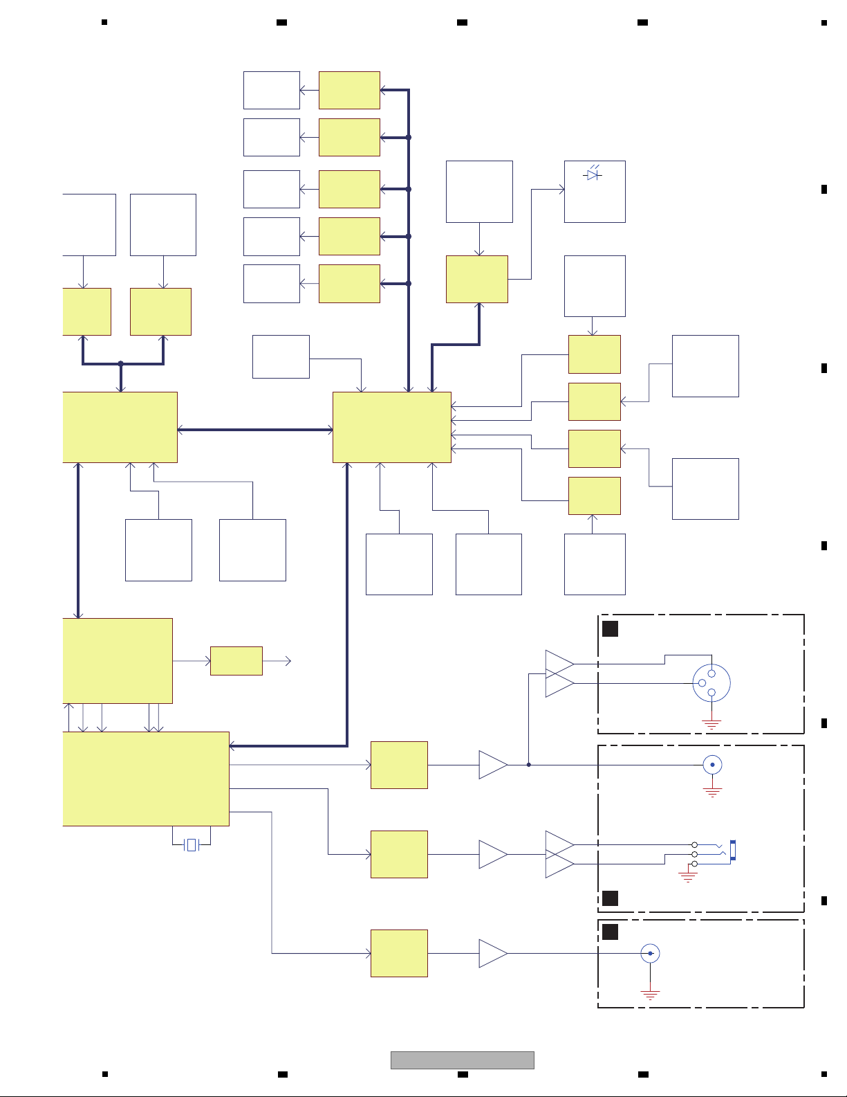
Page 10
1
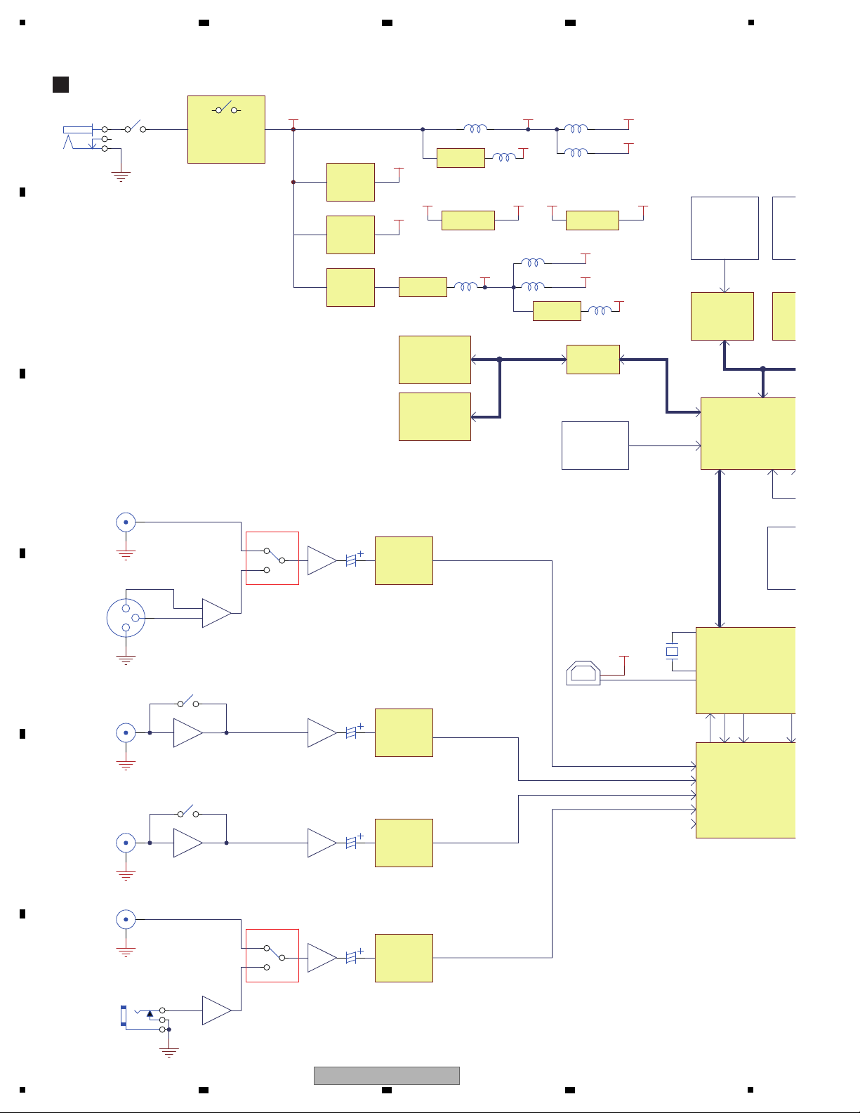
D
DSP PCB ASSY
IC29
IC21
IC30
IC31
IC32
IC33
IC35
IC4
IC6
IC7
IC8
IC5
IC3
IC34
IC1
IC2
IC18
IC28
IC15
IC41
IC40
ADC
PCM1803
DSP567
STM8S207M8
MCU1
(44.1K /24bit/512fs
(I2S format for aud
(24.576M
(16MHz )
ADC
PCM1803
-9.32dB
-9.32dB
LINE3
2
1
3
74HC4052
+36dB(RI AA)
12
ADC
PCM1803
-9.32dB
LI NE2/P HONO2
ADC
PCM1803
CH3
CH1
CH2
CH4
D3.3V
1
2
3
JK1
DC 5V/3A
BA033FP
D5V
D3.3V
BD12AK 5FB
1.20V
12
TP A54232
INVERTER
-15V
TP A61085
BOOST
15V
OVP Limit 5.5V
Ov er Voltage
Protection
12
MI C2
Balance(m ono) +40dB
L
3
G
1
S
4
+36dB(RI AA)
12
LI NE1/P HONO1
2
3
1
MI C1(XL R)
+40dB
-9.32dB
LINE4
2
1
3
74HC4052
USB PortB
TUSB3200
DI 0 DO0 DO1
6M
(12MHz or 48MHz)
LRCK
Vbus
I2C
FSR
AD *
SER.<
P
I/O
SER.<- ->PAL .
PT6961
I/O EXP AND
SPI-2
TACT
KEY
TACT SW * 28
K EY SCAN
AD7147 * 1
RIGHT PANEL
RIGH
NEEDLE SEARCH
LEFT PANEL
LEFT
LEFT PANEL
NEEDLE SEARCH
AD7147 * 1
3.3V<=>5V
BUFFER
SPI-3SPI-3
ENCODE * 2
TACT SW * 4
GPIO * 12
-15V
79L05
-5V
JOG WHEEL *2
5V 1AD5V
2AD5V
TP A61085
BOOST
BA05
A5V
AD5V
DA5V
A3.3V
BA033FP
IC16
IC39
IC17
IC24
4.2 OVERALL BLOCK DIAGRAM
A
B
2 3 4
C
D
E
F
10
1
DDJ-SX
2 3 4
Page 11
5
J
E
F
IC29
IC21
IC20
IC38
IC37
IC36
IC9
IC10
IC13
IC11
IC12
IC25
IC703
FRONT PCB ASSY
OUTPUT PCB ASSY
BAL. PCB ASSY
LPF& .
MASTER OUT
(RCA)
LPF& .
NJM4580
NJM4556
DSP56724
STM8S207M8
MCU1
VR *3
EXP . AD
74HC4051 * 1
SER.<- ->PAL .
PT6961
60LEDs
MAS
(44.1K /24bit/512fs for A/D,D/A)
(I2S format for audio data)
(24.576MHz)
24.576M
(16MHz )
CH FADER * 4
CS FADER * 1
AD * 5
HP
Headphone
(32 ohm/6.3mm & 3.5mm)
DAC
PCM1789
DAC
PCM1754
LED * 36
LED RI NG
LEVEL METER
I/O EXP AND
NJM4580
2
3
1
MASTER OUT
(XLR)
SPI-1
DAC
PCM1754
NJM4580
LPF& .
NJM4580
L
3
R
2
G
1
BOOTH
BOOTH
TUSB3200
0 DO0 DO1
(12MHz or 48MHz)
LRCK BCK
STM8S207M8
MCU2
(16MHz )
SPI-1
I2C
FSR PAD * 8
AD * 8
JOG TOUCH * 2
AD * 2
EXP . AD
74HC4052 * 3
EXP . AD
74HC4051 * 1
EXP . AD
74HC4052 * 1
TEMP O *2
AD * 1
AD * 6
AD * 1
AD * 1
74HC4051 * 1
VR *3
TEMP O *2
VR * 24
3 SLIDE SW * 4
VR * 4
3 SLIDE SW * 4
TACT SW * 20
K EY SCAN
SPI-4
74HC595 * 5
74HC595 * 5
74HC595 * 5
74HC595 * 5
74HC595 * 5
LED * 36
LED RI NG
LED * 47
LED DI MMER
LED * 26
LED DI MMER
LED * 47
LED DI MMER
SPI-5
SER.<- ->PAL .
PT6961
I/O EXP AND
PT6961
SPI-2
TACT SW * 27
K EY SCAN
K EY SCAN
RIGHT PANEL
RIGHT PANEL
RIGHT PANEL
RIGHT PANEL
LEFT PANEL
LEFT PANEL
L&R PANEL
CENTER PANEL
CENTER PANEL
CENTER PANEL
CENTER PANEL
FRONT PANEL
LEFT PANEL
LEFT PANEL
LEFT RING
RIGHT RING
ENCODE * 1
GPIO * 2
MCL K
ICS501
PLL 2X
SCK
AD/DA CL
K
FSR PAD * 8
AD * 8
IC24
6 7 8
A
B
C
D
E
F
DDJ-SX
5
6 7 8
11
Page 12
1
No power. Check that the AC adapter is securely connected.
The AC adapter is in failure.
Replace the AC adapter.
No
Q1 or Q2 is defective.
Replace the defective part.
No
The UCOM (IC24 and IC25) is in failure.
Replace the DSP PCB Assy.
Ye s
Ye s
[1] Abnormality regarding startup and communications
Is 5-V power output from
the AC adapter?
Is 5-V power properly output
from the DSP PCB Assy?
The keys or slide switches do not
function.
Check that the corresponding wires are properly
connected.
Check whether the corresponding switch is defective
or the matrix circuitry is defective.
Direct key
Matrix key
[2] Abnormality regarding the operating elements and LEDs
Is the inoperable switch a direct
or matrix key?
Is there another disabled key in the same
segment (SG**) or on the same signal
line (K**) of the matrix circuitry?
No communication via USB.
Check that the USB cable is securely connected.
Check that the driver has been installed on the connected PC.
The power IC (IC18) is defective.
Replace the DSP PCB Assy.
No
The oscillator (X1) is defective.
Replace the defective part.
No
Turn on the corresponding switch and check
conduction between the two ends of the switch.
If current is not conducted, replace the switch.
No
The USB IC is defective.
Replace the DSP PCB Assy.
Turn on the corresponding switch and check
conduction between the two ends of the switch.
If current is not conducted, replace the switch.
If current is conducted, the UCOM (IC24) is defective.
Replace the DSP PCB Assy.
Ye s
Ye s
If the segment or signal line in question is on
CONTROL PCB Assy A or B, IC505 is defective.
If it is on the MIX PCB Assy, IC703 is defective.
Replace the defective Assy.
If IC505 is defective: CONTROL PCB Assy A, B
If IC703 is defective: MIX PCB Assy
Ye s
Is 3.3-V power properly
output from D3.3V?
Is the oscillator (X1) oscillating
at 6 MHz?
2 3 4
5. DIAGNOSIS
5.1 TROUBLESHOOTING
A
B
C
D
E
F
12
1
DDJ-SX
2 3 4
Page 13
5
The rotary VRs or slide VRs do not
function.
Check that the corresponding wires are properly
connected.
Check that the corresponding wires are properly
connected.
Check that the corresponding wires are properly
connected.
Check the analog SW IC to which the corresponding
signal is connected.
The VR is defective.
Replace the defective part.
No
The analog SW IC is defective.
Replace the corresponding Assy.
Assys to be replaced: CONTROL PCB Assy A, B
MIX PCB Assy
No
No
The UCOM (IC25) is in failure.
Replace the DSP PCB Assy.
Ye s
Ye s
The UCOM (IC25) is in failure.
Replace the DSP PCB Assy.
The UCOM (IC24) is in failure.
Replace the DSP PCB Assy.
Ye s
The rotary selector is in failure.
Replace the defective part.
Ye s
If the defective VR is operated, does
the corresponding signal change?
Is the defective VR a CH fader
or crossfader?
The rotary selectors do not
function.
See "The keys or slide switches do not function."
Pushing
Which operations do not function,
pushing or turning?
Check whether the signals from Pins 1 and 3
of the corresponding rotary selector are
fixed at H when it is turned.
Check whether input signal A, B,
or C is fixed at H or L.
Turning
With BROWSE: The UCOM (IC25) is defective.
With BEATS: The UCOM (IC24) is defective.
Replace the DSP PCB Assy.
No
No
The photo interrupter is defective.
Replace the SENSOR PCB Assy.
Ye s
There is no response to turning of
the jog dial.
Check whether the signals from Pins 2
and 4 of CN501 are fixed at H when
the jog dial is turned.
6 7 8
A
B
C
D
E
F
DDJ-SX
5
6 7 8
13
Page 14
1
The UCOM (IC25) is in failure.
Replace the DSP PCB Assy.
Ye s
The UCOM (IC24) is in failure.
Replace the DSP PCB Assy.
Ye s
Ye s
The PIC UCOM (IC507) is in failure.
Replace the CONTROL PCB Assy A and B.
No
The VR (VR1100 or VR1101) is in failure.
Replace the defective part.
No
Check the Sensitivity Adjustment VR in the
FRONT PCB Assy.
There is no response to pressing of the
jog dial. The sensitivity when the jog dial
is pressed is low.
Check that the corresponding wires are properly connected.
Check soldering of the wires for signals corresponding to
pressing of the jog dial.
Does the voltage at Pin 13 of CN2B in
CONTROL PCB Assy A or B change
in response to pressing of the jog dial?
If there is an abnormality in the waveform of the
signal from Pin 7 of CN5A or CN5B, the sensor IC
(IC475) is defective. Replace the TOUCH PCB Assy.
No
NeedleSearch does not function.
Is there any abnormality in the waveforms
of signals from Pins 1, 2, 4, or 6 of
CN5A or CN5B?
The UCOM (IC24) is in failure.
Replace the DSP PCB Assy.
Ye s
The IC703 is defective.
Replace the MIX PCB Assy.
Ye s
Check the diode of the LED that does not light.
If it is OK, then the IC to which the LED in question is
connected is defective. Replace the corresponding Assy.
Assys to be replaced: CONTROL PCB Assy A, B
MIX PCB Assy
Ye s
The PAD & FSR Assy is in failure.
Replace the PAD & FSR Assy.
No
The LED is defective.
Replace the defective part.
No
Check the transistor to which the LED in question is connected.
If it is OK, then the IC to which the LED in question is
connected is defective. Replace the CONTROL PCB Assy A
or B or the MIX PCB Assy.
No
There is no response to touching
on the PAD.
Do the signals from Pins 2–9 of
CN502 change in response to touching
of the PAD?
The LEDs do not light.
Are the LEDs that do not light
those of a level indicator?
Is there only one LED that does not light?
Does the voltage of the VR signal change
in response to turning of the Sensitivity
Adjustment VR?
Ye s
No
Is there any other LED that does not light
in the same segment (SG**) or on the same
signal line (K**) of the matrix circuitry?
Check that the corresponding wires are properly
connected.
Check that the corresponding wires are properly
connected.
Check that the corresponding wires are properly
connected.
A
2 3 4
B
C
D
E
F
14
1
2 3 4
DDJ-SX
Page 15
5
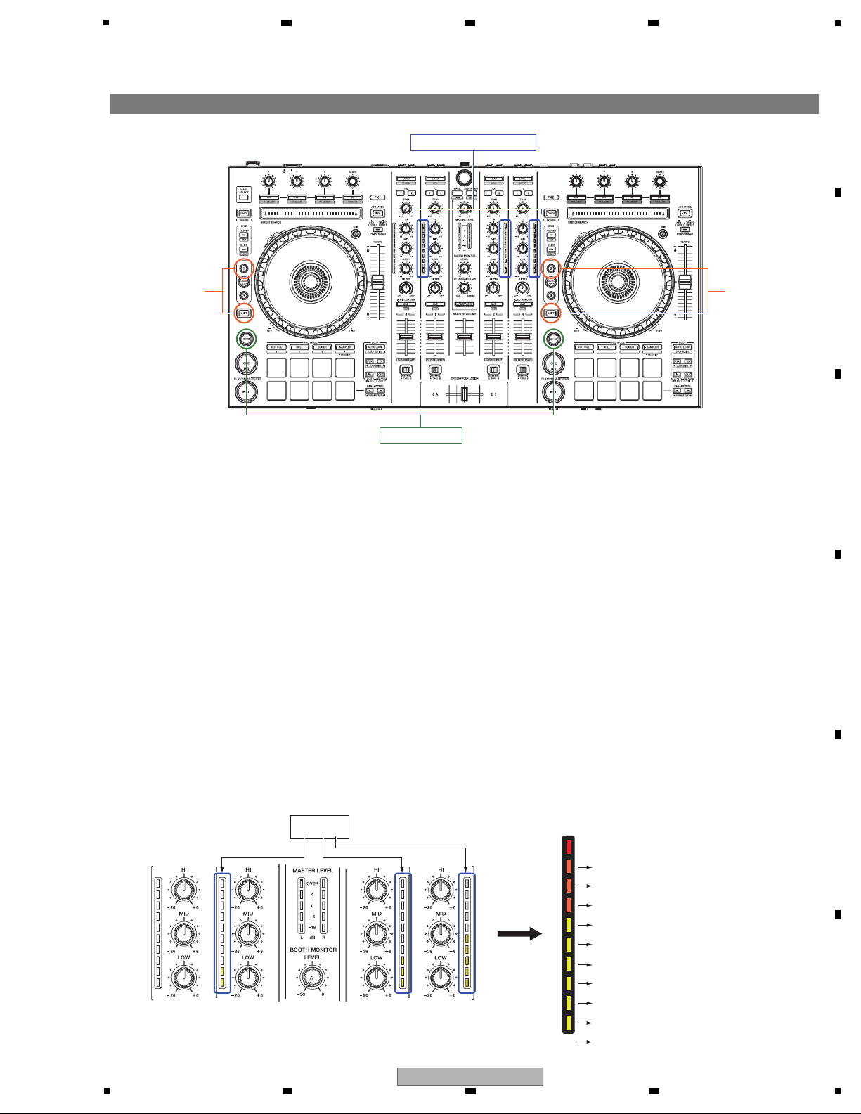
No signal from MASTER OUT.
Check that the corresponding wires are properly
connected.
Check that there is no abnormality in the operating
element system.
Check that the corresponding wires are properly
connected.
Check that there is no abnormality in the operating
element system.
Check that the corresponding wires are properly
connected.
Check that there is no abnormality in the operating
element system.
The audio circuitry is in failure.
Replace the DSP PCB Assy.
Ye s
The muting transistors are in failure.
Replace the defective part.
Ye s
[3] Abnormality in audio input/output
Is no signal output from either
MASTER1 or MASTER2?
Is the audio signal interrupted
around the muting transistors?
No
The audio circuitry is in failure.
Replace the DSP PCB Assy.
No
No signal from either BOOTH OUT
or PHONES OUT.
The muting transistors are in failure.
Replace the defective part.
Ye s
Is the audio signal interrupted
around the muting transistors?
The audio circuitry is in failure.
Replace the DSP PCB Assy.
No
The audio input is not output.
See "No signal from MASTER OUT."
Ye s
Is the level indicator lit?
The audio circuitry is in failure.
Replace the DSP PCB Assy.
No
6 7 8
A
B
C
D
5
6 7 8
DDJ-SX
E
F
15
Page 16
1
[1] Error Alarming
If unusual detection is occurred during Power on or working, Indicate notice by LED.
Error LED Remarks
1
12
Abnormalities in
FLASH-ROM of MAIN_UCOM
The "FX1 Assign" LED of Deck1
Blinks in a cycle of 1 second.
When update goes wrong and FLASH-ROM is not written
correctly, it will be in this state.
If the last update failured, the LED blinks when next Power-on.
Perform updating again. If this error warning persists, replace
the USB cable. If this error warning persists more, replace the
DSP PCB Assy.
2 Abnormalities of USB controller The "FX2 Assign" LED of Deck4
Blinks in a cycle of 1 second.
When the time when it cannot communicate with USB
controller correctly although USB cable is connected at the
time of starting, it will be in this state.
Replace the USB cable. If this error warning persists, replace
the DSP PCB Assy.
2 3 4
6. SERVICE MODE
6.1 SERVICE MODE
A
B
C
D
E
F
16
1
2 3 4
DDJ-SX
Page 17
[2] Service mode
Press and hold the left DECK "SHIFT" button and the left "DECK 1" button, then Power-ON.
or
Press and hold the right DECK "SHIFT" button and the right "DECK2" button, then Power-ON.
The firmware version is displayed first. LED except it turn off.
[Method to enter]
Power-OFF
[Method to exit]
When in this mode, the firmware version display appear first.
In this mode, it does not work to communicate with computer via USB.
In this mode, LED dimmer is not available.
[Note]
Firmware version (x.xx)
Factory Reset
into
Service mode
into
Service mode
This display is released by any operation (Channel faders) .
Then all LED is turned off.
After this mode starts, the firmware version is displayed first.
The format of the firmware version is "x.xx". (x: decimal)
It is displayed by the Channel level indicators (Deck1/Deck2/Deck4).
x.xx
This figure is example of "ver2.35".
9
1. Check of the Firmware Version
8
7
6
5
4
3
2
1
0 (all off)
5
6 7 8
A
B
C
D
5
DDJ-SX
6 7 8
E
F
17
Page 18
1
LED lighting specification for parts type
In case of the left parts, the left parts LED are lit.
In case of the right parts, the right parts LED are lit.
In case of the center parts, the right&left parts LED are lit.
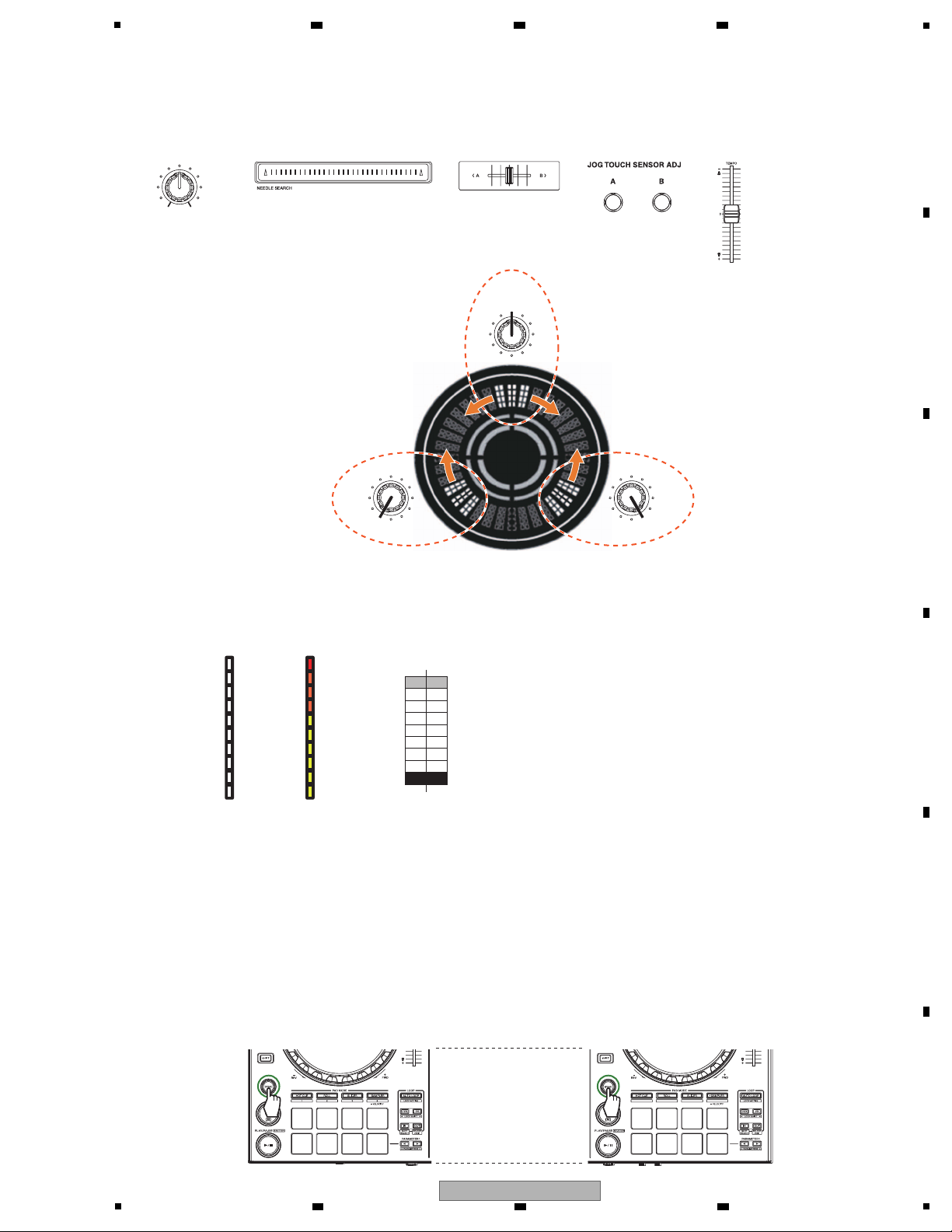
The indication corresponding to a pressed button is lit only while the button is held pressed.
(Press and hold the left LOOP"IN" button and the left "F2" button then power-on. Keep it until opening illumination is terminated.)
In case of the rotary type (knobs, jog dial), LED are assigned
360 degree in 36 steps.
In case of the selector type, LED are assigned 1 click by 1 step.
The starting position depends on the last position.
One unit to light consists of three LED and they are always lit.
Rotary type Selector type
[Note]
(*1) TYPE A (Rotary knob, Jog dial)
After checking the firmware version, you can check if each UI parts (button/jog dial/knob/fader etc.) are not abnormal.
All UI parts of top&front panel are objects to check.
2. Check of UI parts & LED
Parts type UI Parts Name Trigger LED to check
Push switches (with LED)
Rotary knob, jog dial (rotate)
Press Own LED
Turn "Jog dial center LED" TYPE-A (*1)
NEEDLE SEARCH Pad, Cross fader, TEMPO slider Slide "Jog dial center LED" TYPE-B (*2)
Channel fader Slide Each channel level indicator (*3)
Slide Jog dial center LED TYPE-A (*1)
Push switches (without LED)
Slide switch
"BROWSE"
"BACK"
"AREA"
"JOG (touch)"
"PANEL"
"SHIFT"
CRF ASSIGN SW
INPUT SELECT SW
Press
All LEDs and indicators
CH FADER START (DECK1) LED
SYNC (DECK2) LED
"Jog dial center LED" all on
"REV"LED
"HOT CUE" LED
A
2 3 4
B
C
D
E
F
18
1
2 3 4
DDJ-SX
Page 19
5
In these type, the position is indicated in 27 steps from minimum to maximum.
One block consists of three LED.
In channel fader, the position is indicated in 11 steps from minimum to maximum.
The each channel fader (Deck1 - Deck4) is indicated at own Channel level indicator.
(CH1 → CH1 level indicator, CH2 → CH2 level indicator, etc.)
CENTER
MIN
MIN
MIN
MAX
MAX
MAX
(*2) TYPE B (Volume knob, NEEDLE SEARCH Pad, Cross fader, TEMPO slider)
(*3) Check for Channel fader
The following data is reset to the factory default settings by "Factory reset" operation.
• Setting data in Utility mode
• Last memory of users
3. Factory Reset
Press and hold the left DECK "SYNC" button and the right DECK "SYNC" button for 5 seconds.
Then factory reset starts and "SYNC"LEDs are lit.
After completing reset, "SYNC" LEDs are turned off.
5 seconds 5 seconds
[Method to reset]
6 7 8
A
B
C
D
DDJ-SX
5
6 7 8
E
F
19
Page 20
1
[3] Measurement mode
Press and hold the "SHIFT"+"DECK3" buttons then Power-ON.
During this mode, "DECK 3" and "DECK 4" LEDs are lit.
This is the mode to measure jog dial rotation time and the fluctuation of knobs/faders.
(1) Jog dial Rotation Time measurement mode
(2) Volume value fluctuation check mode
[Method to enter]
Power-OFF
[Method to exit]
1 You spin Jog dial more than 33*7 = 231 rpm.
*1 In case of less than 231 rpm, it is failure. Then "SLIP" LED is lit.
*2 You must measure by either clockwize or counterclockwize.
2 The controller measures "T1".
*T1: The time that Jog dial rotation speed slow down from 100 rpm to 50 rpm.
3 The controller display result with three Channel level indicators. Refer to below.
The format of the result is "XXX" msec. (X: 0-999 msec .decimal)
It is displayed by the Channel level indicators (Deck1/Deck2/Deck4).
[Method to measure]
This is the mode to measure the JOG rotation time which is specified at "Jog dial Performance specification".
In case of the left jog dial, the result are displayed at the left LEDs.
In case of the right jog dial, the result are displayed at the right LEDs.
The specified range is 100 ± 40 msec.
(1) Jog dial Rotation Time measurement mode
Volume value fluctuation check mode
Jog dial Rotation Time measurement mode
into
Measurement mode
x.xx
The above figure is example of "235msec".
9
8
7
6
5
4
3
2
1
0 (All off)
A
2 3 4
B
C
D
E
F
20
1
2 3 4
DDJ-SX
Page 21
5
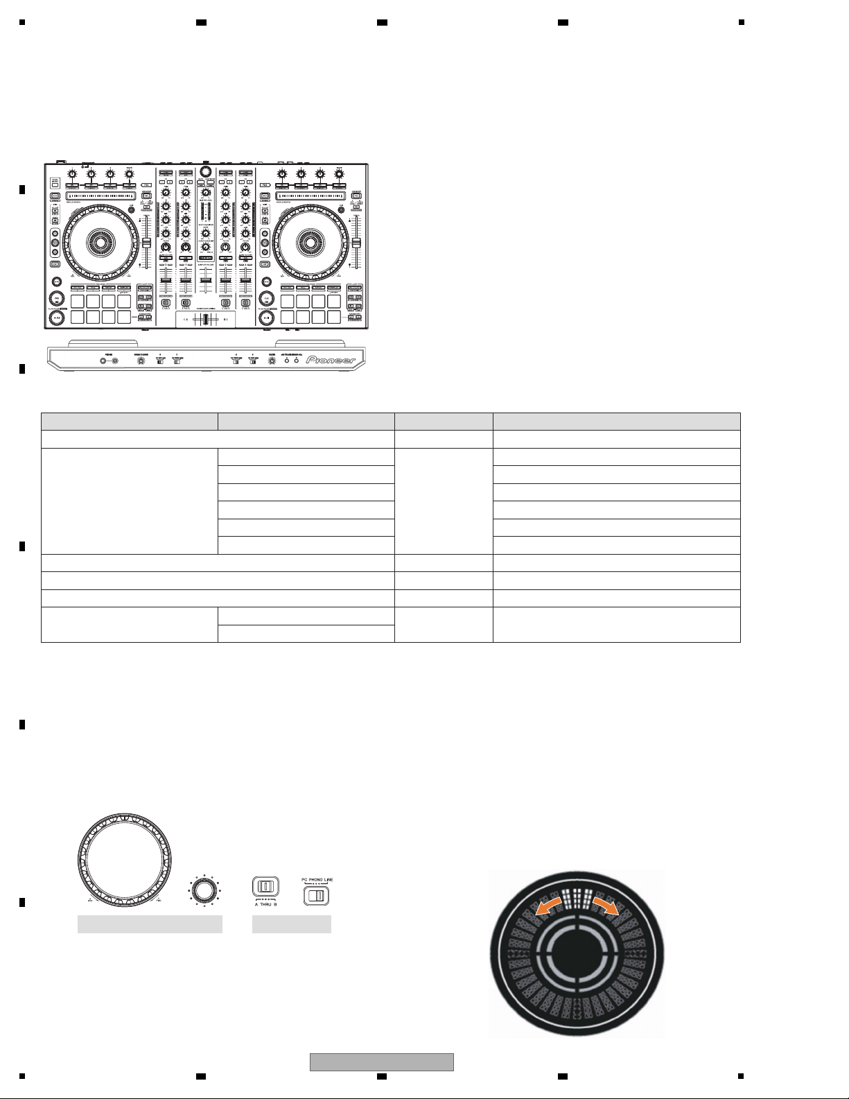
11 2 3
5
2222
3535
1818
1919
2020
3636 3737
3939
2121 2828
2626
2727
2323
2424 2525
3434
3232
3333
2929
3030 3131
6
7
9
1010
1111
8
1212
1515
1515
1616
1313 1414
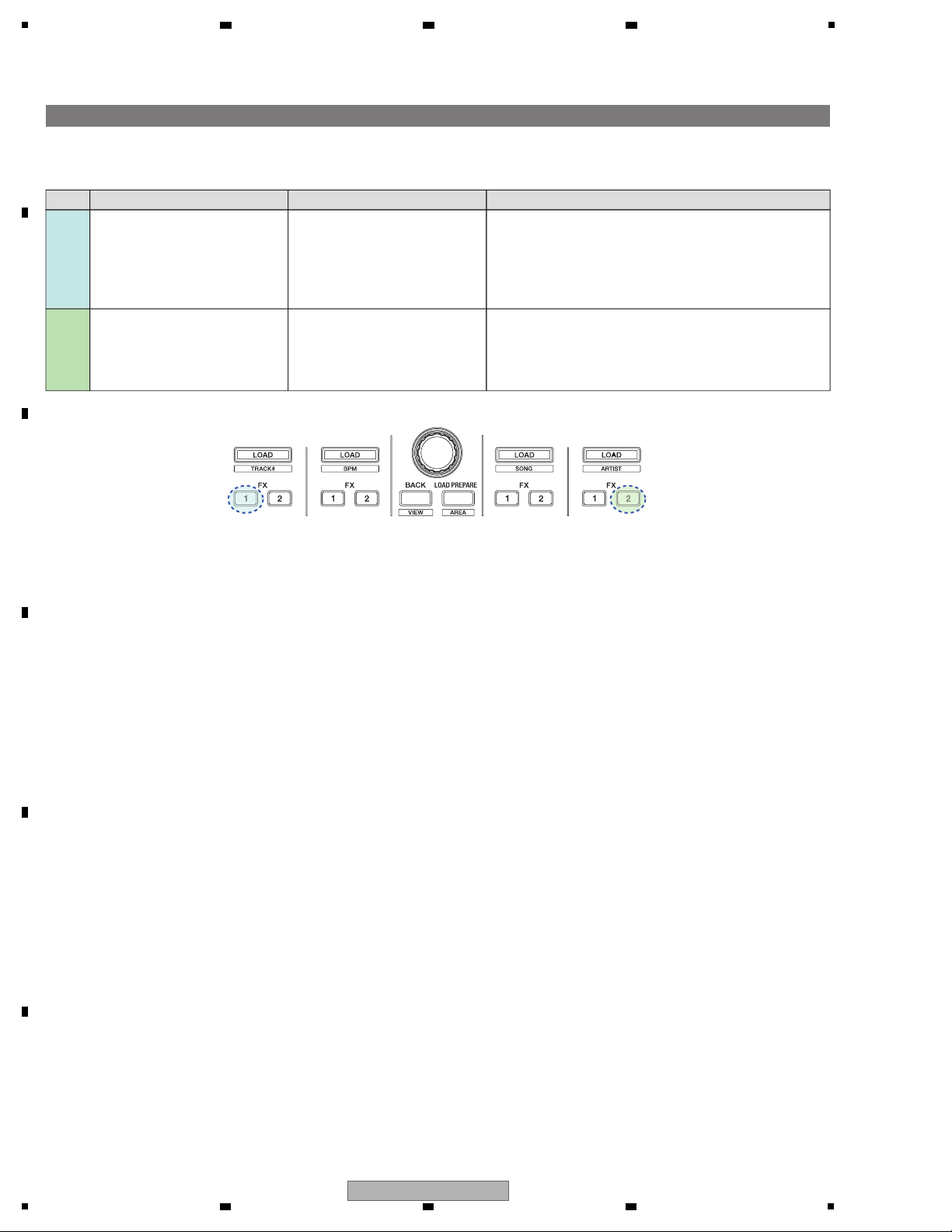
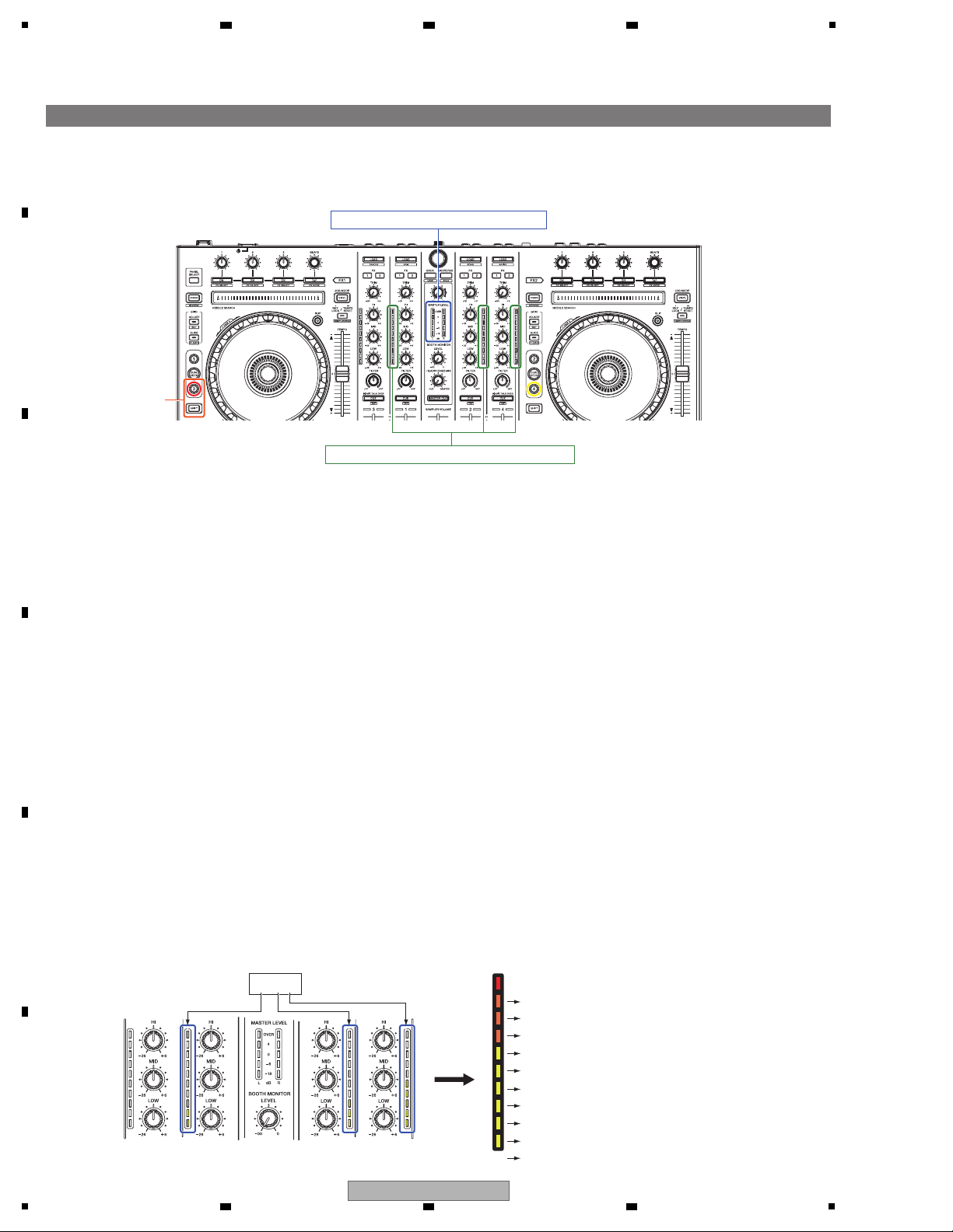
Will be tested fluctuation of voltage (A/D conversion value) which is made each Fader and Rotary volume by Master level
indicator.
[Overview]
Knobs under test operation are filled blue as below.
Test subjects to move by turning right / left-turn Rotary selector.
A/D conversion value observation start/reset by push the Rotary selector.
[Knobs under test operation]
1 Choose the test subject by turn left and right Rotary selector.
The LED is lit with the following turns every 1 click.
Turn right: 1 → 2 → 3 → 5 → . . . . . → 37 → 39 → 1 → . . .
Turn left: 39 → 37 → 36 → . . . . . → 2 → 1 → 39 → . . . (No.4 and 38 were deleted)
Note: Regarding No.22, both LED are lit.
2 You can see what knob/fader is selected by Lighting LED on each button as shown in the above figure.
For example ,LED to test "SAMPLER VOLUME" fader is "MASTER CUE" button's LED.
3 When targeted knob is decided, push the Rotary selector and start observation of A/D conversion value.
Get the A / D conversion value immediately after the start. It will be reference value.
*A/D conversion value to be monitored is Raw data.
4 Start monitoring and later to monitor the A/D conversion value, do the following actions depending on its value with
Master level indicator.
[Test detail]
• For failure judgment of the rotary VRs
As a guide, amplitude values higher than +4 or lower than -4 may be judged as failure.
The VRs can be set to any position during measurement. Possible symptoms are shown below.
• The volume changes arbitrarily.
• Interrupted sound leakage occurs even if the volume is decreased to the minimum at the Master or Booth Monitor.
• The MIDI signal is output even if the corresponding VR is not operated.
• For operation check of a rotary VR after replacement
[Use of this mode during repair]
(2) Volume value fluctuation check mode
6 7 8
A
B
C
D
E
DDJ-SX
5
6 7 8
F
21
Page 22

1
Result Fig No.
+1 from the reference value A/D conversion value
* Display at the same time both fall / rise direction from the reference
value of the conversion value A/D.
* Keep the lighting position at the time of maximum fluctuation of
each of the positive & negative direction
1
+2 from the reference value A/D conversion value 2
+3 from the reference value A/D conversion value 3
+4 from the reference value A/D conversion value 4
Over +5 From the reference value A/D conversion value
5
-1 from the reference value A/D conversion value 6
-2 from the reference value A/D conversion value 7
-3 from the reference value A/D conversion value 8
-4 from the reference value A/D conversion value 9
Less than -5 from the reference value A/D conversion value
10
5 By pushing the Rotary selector while monitoring the conversion value A/D, it is possible to reset the state of the fluctuations
of the past.
Ex.)
1. Turn EQ HI knob (for DECK 1) to the position you want to
measure.
7. More time has elapsed, Master level indicator is lit as
follows: become the value 758 of the A/D.
8. More time has elapsed, To maintain the above display
759 even though the value of the A/D.
9. More time has elapsed, Master level indicator is lit as
follows: become the value 757 of the A/D.
10. Off all the LED on Master level indicator When you push
the Rotary selector, and this value will be new reference
value.
2. Turned right 11 clicks Rotary selector.
→ "FX1 assign" LED of the DECK 1 is lit.
3. Start A/D conversion value monitoring to push Rotary
selector. If A/D value of push the Rotary selector is 760,
to monitor the amount of change in the value of A/D as
a reference value 760.
4. After a while, Master level indicator is lit as follows:
become the value 763 of the A/D.
5. More time has elapsed, to maintain the above display
762 even though the value of the A/D.
6. More time has elapsed, Master level indicator is lit as
follows: become the value 764 of the A/D.
12345678 910
DECK1
A
B
2 3 4
C
D
E
F
22
1
2 3 4
DDJ-SX
Page 23

5
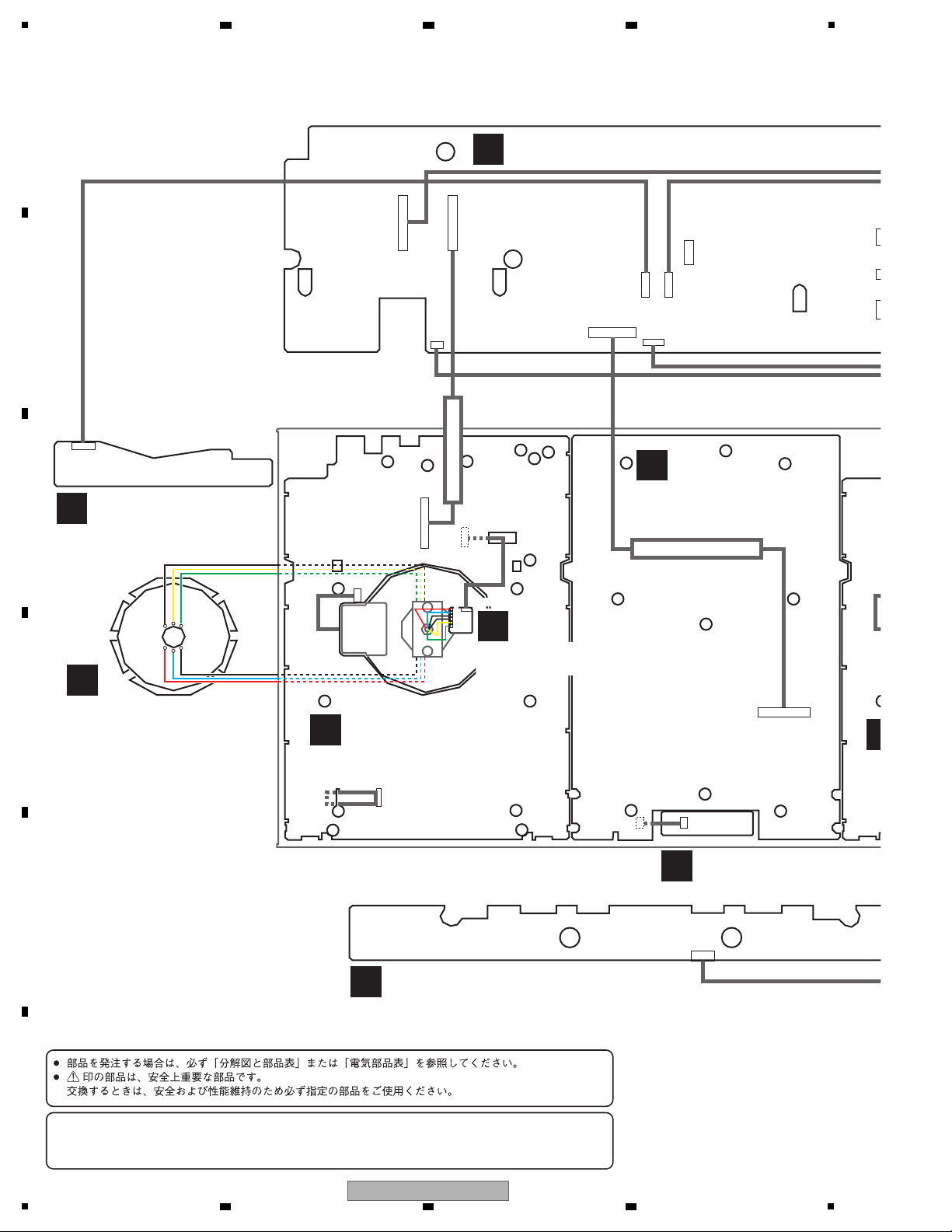
[1] DSP and OUTPUT PCB Assemblies
• Base
• Shield
(1) Remove the Base by removing the 21 screws.
(602-PTP3012-571-HA)
(1) Remove the two screws.
(602-MP3-324-HA)
(2) Remove the Isolation plate by removing the
two screws.
(602-B600-072-HA)
(3) Remove the two screws.
(602-SL24F-099-HA)
(4) Remove the one screw.
(602-QMX2BPM-322-HA)
(5) Remove the Cover by removing the one screw.
(602-B600-072-HA)
Isolation plate
Cover
Base
• Bottom view
• Bottom view
1
2
5
4
3
3
2
1
1
2 3
4 5
6
7
8
9
10
11
12
13
14
15
16
1718
19
20
21
Screw tightening order
1
×21
• DSP and OUTPUT PCB Assemblies
(1) Remove the Strain relief bush by removing
the one screw.
(602-BTB3012-446B-HA)
(2) Remove the four screws.
(602-MP3-324-HA)
(3) Remove the Ground terminal and washer.
• Rear view
2 2
3
2 2
1
12 43
Screw tightening order
Note: Even if the unit shown in the photos and illustrations in this manual may differ from your product, the
procedures described here are common.
Disassembly
6 7 8
7. DISASSEMBLY
A
B
C
D
E
5
DDJ-SX
6 7 8
F
23
Page 24

1
(4) Cut the binder
(5) Disconnect the one flexible cable and two
connectors.
(CN1B, CN4B, W9)
(6) Remove the Output board by removing the
eight screws.
(602-B600-072-HA)
(7) Disconnect the two flexible cables and three
connectors.
(CN2Bx2, CN5A, CN5B, CN7)
Earth lead
DSP PCB Assy
CONTROL PCB Assy B
FRONT PCB AssyMIX PCB Assy
CONTROL PCB Assy A
OUTPUT PCB Assy
Earth lead
• Bottom view
• Bottom view
5
6
6
6
6
6
6
6
6
5
5
4
7
7
7 7
7
CN4B
CN1B
CN7
CN5A CN5B
CN2B CN2B
W9
1
7
8
9
10
11
3
4
5
6
2
Screw tightening order
Screw tightening order (referemce information)
1
1
10
2
67
8
9
3
4
5
67 2 3
4
5
A
2 3 4
B
C
D
E
F
24
DDJ-SX
1
2 3 4
Page 25

5
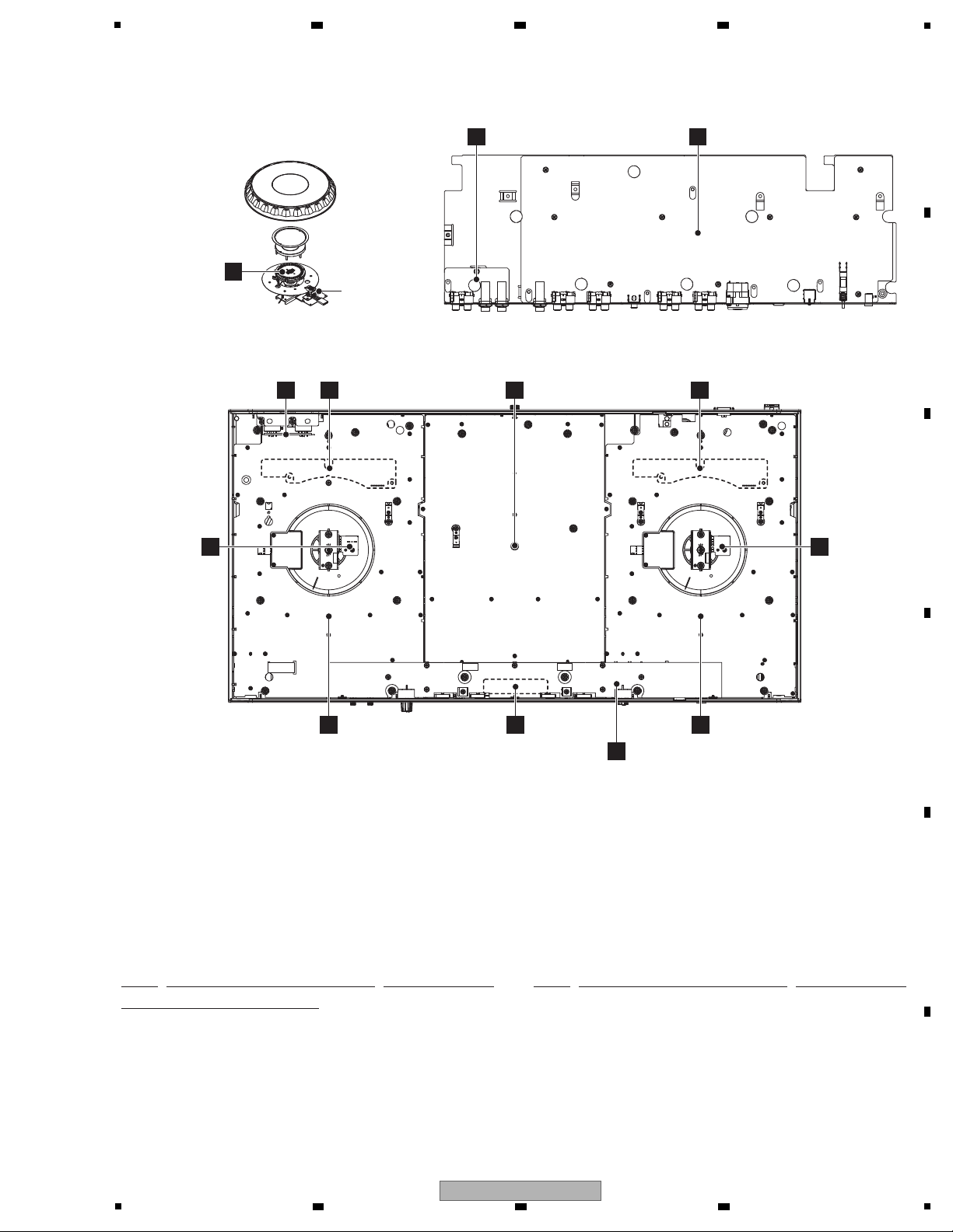
[2] Jog dial section
• SENSOR PCB Assy
(1) Remove the Dust-proof slice by removing the
two screws.
(602-PROS2-363-HA)
• Jog dial section
(1) Remove the six solders.
(2) Remove the one nut and one washer.
(3) Remove the JW LED base by removing the
two screws.
(602-3113-122-HA)
(4) Remove the one E ring.
(2) Disconnect the one connector.
(CN501)
(3) Remove the Sensor fixed plate by removing
the two screws.
(602-DJ5500-452-HA)
(4) Remove the SENSOR PCB Assy.
Note:
A figure is only left DECK side, but the right side
is similar, too.
Dust-proof slice
Sensor fixed plate
SENSOR PCB Assy
TRANSFER PCB Assy
JW LED base
1
3
1
4
3
3
2
3
4
1
2
CN501
• Bottom view
• Bottom view
• Bottom view
• Bottom view
6 7 8
A
B
C
D
E
DDJ-SX
5
6 7 8
F
25
Page 26

1
(5) Remove the jog dial section.
Jog dial section
5
(2) Remove the LED and Cover Assy.
(3) Remove the JW cover by unhooking the six
hooks.
(4) Remove the LED PCB Assy.
1
3
4
3
3
3
3
3
3
2
Jog dial section
JW cover
LED PCB Assy
LED and Cover Assy
Windows lens
• Bottom view
• LED PCB Assy
(1) Remove the Windows lens.
Insert a slim rod in the hole for disassembly
in the jog dial section bottomside, and remove it.
Hole
• Bottom view
A
B
2 3 4
C
D
E
F
26
1
DDJ-SX
2 3 4
Page 27

5
[3] Each PCB Assemblies
• BAL. PCB Assy
(1) Remove the BAL. PCB Assy by removing the
two screws.
(602-DJ5500-452-HA)
• CH FADER PCB Assy
(1) Remove the Push button.
(2) Remove the CF board by removing the two
screws.
(602-CTF3010-698B-HA)
(3) Remove the CH FADER PCB Assy.
(4) Disconnect the one connector.
(CN01)
• FRONT PCB Assy
(1) Remove the two Gain rotate knobs.
(2) Remove the three screws.
(602-MP3-324-HA)
(3) Remove the FRONT PCB Assy by removing
the seven screws.
(602-DJ5500-452-HA)
Note:
When you remove each PCB Assemblies, it is not
necessary to remove a jog dial section.
BAL. PCB Assy
Push buttonCF board CH FADER
PCB Assy
CH FADER PCB Assy
FRONT PCB Assy
1
1
2 2
2
3 3
3 3 3
3 3
2
1
2
1
• Bottom view
• Bottom view
1
1
2
4
5
6
7
3
23
Screw tightening order
1
3
4
CN01
6 7 8
A
B
C
D
5
DDJ-SX
6 7 8
E
F
27
Page 28

1
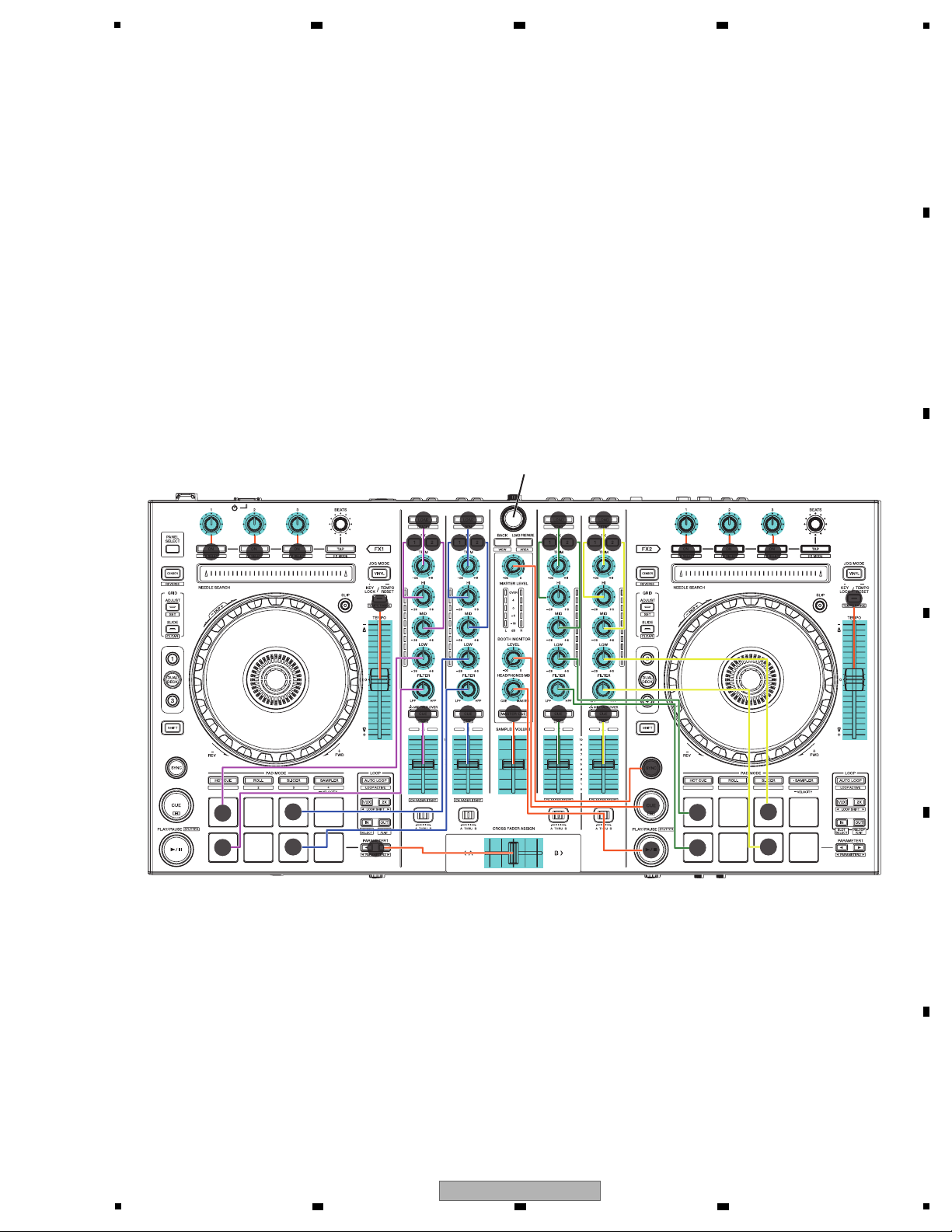
• CONTROL and MIX PCB Assemblies
(1) Remove the all knobs.
(2) Remove the Front panel by removing the
33 screws.
(602-HP1010K-182-HA)
1
×29
2
×33
Front panel
Applicable models by destination
For UXECB: SER1101 or later
For FLPXE: SER0151 or later
Other destinations: From first production
NITTO No. 500
(5 mm × 40 mm)
When detaching the front panel
The front panel and the Chassis Assy are secured with 4 pieces of double-back tape at the locations shown in the photo below.
Slowly peel off the tape, taking care that you will not deform the front panel.
When reattaching the front panel
1 Neatly remove any residue of double-back tape from the back of the front panel and the Chassis Assy.
2 Stick 4 pieces (5 mm × 40 mm) of NITTO No. 500 double-back tape to the locations shown in the photo below then remove the paper liner.
Note: Even if double-back tape was not used in the initial state, be sure to attach double-back tape when reattaching the front panel.
About the double-back tape that is used for securing the front panel and the Chassis Assy
A
B
2 3 4
C
D
E
F
28
1
2 3 4
DDJ-SX
Page 29

5
(5) Remove the Isolation slice by removing the
five screws.
(602-SL24F-099-HA)
(6) Remove the Ground plate by removing the
four screws.
(602-SL24F-099-HA)
(7) Disconnect the two flexible cables and four
connectors.
(CN500x2, CN501x2, CN502x2)
(8) Remove the two solders.
(9) Remove the MIX PCB Assy by removing the
14 screws.
(602-SL24F-099-HA)
(10) Remove the CONTROL PCB Assy A by
removing the 18 screws.
(602-SL24F-099-HA)
(11) Remove the CONTROL PCB Assy B by
removing the 17 screws.
(602-SL24F-099-HA)
CONTROL
PCB Assy B
CONTROL
PCB Assy A
MIX PCB Assy
• Bottom view
9
×14 ×18
11 10
×17
1
5
2
4
7
3
8
9
10
11
12
13
14
15
19
22
20
21
23
16
17
18
6
Screw tightening order
The other screws are random order.
5
Isolation slice
5
6
6
5
5
5
• Bottom view
6
6
7
7
7
CN502
CN501
CN500
7
CN500
7
CN501
7
CN502
8
(3) Remove the 22 nuts and 22 washers.
(4) Remove the 10 screws.
(602-2002-077-HA)
3
×22
4
×10
6 7 8
A
B
C
D
E
F
DDJ-SX
5
6 7 8
29
Page 30

1
Adhesive
(GYL1001)
Adhesive
(GYL1001)
Adhesive
(GYL1001)
Adhesive
(GYL1001)
Grease
(GEM1072)
Grease
(GEM1072)
Adhesive
(GYL1005)
• Bottom view
SENSOR
PCB Assy
JW LED base
Sponge
DSP PCB Assy
Chassis Assy
Jog dial section
Washer
SENSOR PCB Assy SENSOR PCB Assy
CH fader fixed plate
MIX PCB Assy
Grease
(GEM1072)
Adhesive
(GYL1005)
Adhesive
(GYL1005)
The Application Position of Adhesive and Grease
TOUCH PCB Assy TOUCH PCB Assy
• Bottom view
1 1
1
1
1
1
• TOUCH PCB Assy
(1) Remove the two TOUCH PCB Assemblies by
removing the six screws.
(602-B600-057-HA)
A
2 3 4
B
C
D
E
F
30
1
2 3 4
DDJ-SX
Page 31

5
After repairing, be sure to check the version of the firmware, and if it is not the latest one, update to the latest version.
Perform the each item when the following parts are replaced.
• IC storing firmware and PCB Assy
IC24, IC25 (DSP PCB Assy),
DSP PCB Assy
• Confirmation of the version of the firmware
• Updating to the latest version of the firmware
• When replaced WHEEL Assy
• Confirmation of the specified value by the mode which
measures rotary decline time of the jog dial
1 Connect the above prepared computer to DDJ-SX via the
USB cable included with the product.
3 When the update file for DDJ-SX (DDJ-SX_Vxxx.jar) is
activated, the following dialogue is displayed.
Click the [Start] button.
4 The update of the firmware starts.
2 Turn on the power of DDJ-SX while pressing the [SHIFT]
button and the [SYNC] button on the LEFT deck ensure
the Level meter LEDs flash before releasing your finger
from the these buttons.
Computer (USB)
AC adapter
(DC IN)
Updating procedures
• Update file for DDJ-SX
* When the downloaded zip file is double-clicked, the update file is unzipped.
Example) DDJ-SX_V101.jar
• A computer where Java has been installed.
* If Java has not been installed, please download the Java Runtime Environment (JRE)
at: http://java.com and install it on your computer.
What you need for updating
6 7 8
8. EACH SETTING AND ADJUSTMENT
8.1 NECESSARY ITEMS TO BE NOTED
A
B
8.2 UPDATING OF THE FIRMWARE
C
D
E
5
DDJ-SX
6 7 8
F
31
Page 32

1
5 When the firmware update process is complete, click the
[OK] button.
Please note that if you fail to update, turn on the power of
DDJ-SX again and start from Step 3 of the above Updating
Procedures.
How to check the firmware version
ASIO driver exclusively for DDJ-SX is required to be installed.
From the [Start menu],
Run [All the programs] → [Pioneer] → [DDJ-SX] →
[DDJ_SX Version Display Utility]
[For Windows]
Open the Apple menu while pressing the option key, then
select “System Profiler.”
Select the [USB] from the [Hardware] to display the name of
the controller. Select the controller to display the firmware
version.
[For Mac]
1.01
A
2 3 4
B
C
D
E
F
32
DDJ-SX
1
2 3 4
Page 33

5
Item for Which User's
Setting is Available
Setting Value (The factory default
settings are indicated in bold.) / Indication method
Content to be
Stored
This unit is provided with user settable items, as shown below.
Settings for DJ software other
than Serato DJ
Serato DJ:
Software other than Serato DJ:
/ [KEY LOCK] unlit
/ [KEY LOCK] lit
Change of the Master
Attenuator setting
0 dB (without attenuation):
–3 dB:
–6 dB:
/[HOT CUE] mode button lit
/[ROLL] mode button lit
/[SLICER] mode button lit
Setting for flashing in
Slip mode
Flashing in Slip mode enabled:
Flashing in Slip mode disabled:
/[SLIP] button lit
/[SLIP] button unlit
Demo mode setting
Demo mode enabled:
Demo mode disabled:
/[TAP] button lit
/[TAP] button unlit
Velocity curve setting for
SAMPLER VELOCITY mode
Curve 1 (Linear):
Curve 2:
Curve 3:
Curve 4 (3 steps):
/[LOOP 1/2X] button lit
/[LOOP 2X] button lit
/[LOOP IN] button lit
/[LOOP OUT]button lit
Illumination mode setting for
the jog dial
Pattern 1 without dimmer:
Pattern 2 without dimmer:
Reverse pattern 1 without dimmer:
Reverse pattern 2 without dimmer:
Pattern with dimmer:
/Only the PAD1 LED lit
/Only the PAD2 LED lit
/Only the PAD3 LED lit
/Only the PAD4 LED lit
/Only the PAD5 LED lit
MIDI setting for SAMPLER
VELOCITY mode
3 ms:
4 ms:
13 ms:
/Number of LEDs of the level indicator lit: 0
/Number of LEDs of the level indicator lit: 1
/Number of LEDs of the level indicator lit: 10
UTILITY setting
Setting value
Part Name
IC24
(DSP PCB Assy)
Channel fader start setting
Channel fader start with sync:
Channel fader start without sync:
Channel fader start function disabled:
/Left Effect Parameter button lit
on the left deck
/Center Effect Parameter button
lit on the left deck
/Right Effect Parameter button
lit on the left deck
Each of the above items can be set in Utility mode.
To enter Utility mode, while holding the SHIFT and PLAY/PAUSE f buttons on the left deck pressed, turn the unit ON.
During Utility mode, the PLAY/PAUSE LEDs on both decks are lit.
After Utility mode is entered, the current setting for each item is indicated with the corresponding LED.
(For details, refer to the operating instructions.)
8.3 ITEMS FOR WHICH USER SETTINGS ARE AVAILABLE
6 7 8
A
B
C
D
E
F
DDJ-SX
5
6 7 8
33
Page 34

1
NOTES: - Parts marked by “NSP” are generally unavailable because they are not in our Master Spare Parts List.
-
The > mark found on some component parts indicates the importance of the safety factor of the part.
Therefore, when replacing, be sure to use parts of identical designation.
-
Screws adjacent to b mark on product are used for disassembly.
-
For the applying amount of lubricants or glue, follow the instructions in this manual.
(In the case of no amount instructions, apply as you think it appropriate.)
FLPXE only
SVYXE8,
FLPXE
only
2 3 4
9. EXPLODED VIEWS AND PARTS LIST
A
9.1 PACKING SECTION
B
C
D
E
F
34
1
2 3 4
DDJ-SX
Page 35

5
6 7 8
(1) PACKING SECTION PARTS LIST
Mark No. Description Part No.
> 1 AC Adapter See Contrast table (2)
> 2Power Plug See Contrast table (2)
> 3Power Plug See Contrast table (2)
> 4Power Plug See Contrast table (2)
> 5Power Plug See Contrast table (2)
6 USB Cable 408-100UG-087-HA
7 CD-ROM (Installation Disc) 429-S1-142-HA
8 Read Before Use (Important)/ See Contrast table (2)
Quick Start Guide
9 Handle 100-DDJLE-3012-HA
A
10 Handle Base 100-DDJLE-3013-HA
11 Polyfoam BL 506-SX-648BL-HA
12 Polyfoam BR 506-SX-648BR-HA
13 Polyfoam FL 506-SX-648FL-HA
14 Polyfoam FR 506-SX-648FR-HA
15 Paster board 507-S1-3372-HA
16 Gift Box See Contrast table (2)
17 Soft Bag 509-DDJSX-320-HA
(2) CONTRAST TABLE
DDJ-SX/UXECB, SVYXE8, FLPXE, AXE5 and KXE5 are constructed the same except for the following:
Mark No. Symbol and Description
> 1 AC Adapter 411-S1-878-HA 411-S1-879-HA 411-S1-880-HA 411-S1-881-HA 411-S1-882-HA
> 2Power PlugNot used 420-DJM250-362-HA 420-DJM250-364-HA Not used Not used
> 3Power PlugNot used Not used 420-DJM250-363-HA Not used Not used
> 4Power PlugNot used Not used 420-DJM250-362-HA Not used Not used
> 5Power PlugNot used Not used 420-DJM250-361-HA Not used Not used
8 Read Before Use (Important)/
Quick Start Guide (En)
8 Read Before Use (Important)/
Quick Start Guide
(En, Fr, De, It, Es, Po, Py)
8 Read Before Use (Important)/
Quick Start Guide (En)
Read Before Use (Important)/
8
Quick Start Guide (Zhcn)
8 Read Before Use (Important)/
Quick Start Guide (Ko)
DDJ-SX
/UXECB
502-DDSXA-3277-HA Not used Not used Not used Not used
Not used 502-DDSXB-3278-HA Not used Not used Not used
Not used Not used 502-DDSXF-3282-HA Not used Not used
Not used Not used Not used 502-DDSXD-3280-HA Not used
Not used Not used Not used Not used 502-DDSXE-3281-HA
DDJ-SX
/SVYXE8
DDJ-SX
/FLPXE
DDJ-SX
/AXE5
DDJ-SX
/KXE5
B
C
D
16 Gift Box 507-S1-3370A-HA 507-SXB-3370A-HA 507-SXF-3370A-HA 507-SXD-3370-HA 507-SXE-3370-HA
DDJ-SX
5
6 7 8
E
F
35
Page 36

1
H
K
C
C
NSP
NSP
NSP
9.2 EXTERIOR SECTION
A
B
2 3 4
C
D
E
F
36
1
2 3 4
DDJ-SX
Page 37

5
A
B
D
E
F
G
I
J
J
6 7 8
A
B
C
D
E
F
DDJ-SX
5
6 7 8
37
Page 38

1
EXTERIOR SECTION PARTS LIST
Mark No. Description Part No.
1 CONTROL PCB Assy A 704-DDJS1-A421-HA
A
2 CONTROL PCB Assy B 704-DDJS1-A454-HA
3 TRANSFER PCB Assy 704-DDJS1-A429-HA
4 DSP PCB Assy 704-DDJS1-A418-HA
5 OUTPUT PCB Assy 704-DDJS1-A425-HA
6 BAL. PCB Assy 704-DDJS1-A423-HA
7 MIX PCB Assy 704-DDJS1-A417-HA
8 CH FADER PCB Assy
9 FRONT PCB Assy 704-DDJS1-A424-HA
10 TOUCH PCB Assy 704-DDJS1-A426-HA
2 3 4
No. Description Par t No.
Mark
46 CUE Button 100-S1B-2993-HA
47 2X Button 100-S1B-2994-HA
48 VINYL Button 100-S1C-2989-HA
49 DECK 4 Button 100-S1C-2990-HA
50 MASTER CUE Button 100-S1C-2993-HA
tton 100-S1C-2994-HA
51 Bu
LOAD Button 100-S1D-2993-HA
52
704-DJM250-A032-HA
53 AUTO LOOP Button 100-S1E-2993-HA
54 S.S Button 100-S1F-2993-HA
55 H.R Button 100-S1G-2993-HA
B
11 LED PCB Assy 704-DDJS1-A422-HA
12 SENSOR PCB Assy 704-PDJ33-A007-HA
13 PAD & FSR Assy 704-S1-A458-HA
14 LED & COVER Assy 704-DDJS1-A455-HA
15 Power Knob
100-HDJ2000-1641-HA
16 Rectangular Button 100-SX-2989S-HA
17 Windows Lens 100-S1-2985-HA
18 SHIFT Button 100-S1-2989-HA
19 DECK 1 Button 100-S1-2990-HA
C
20 LITTLE ROUND Button 100-S1-2991-HA
21 2 Key Button 100-S1-2992S-HA
22 ON Button 100-S1-2993-HA
23 1,2 Button 100-S1-2994-HA
24 PLAY SYNC Button 100-S1-2995-HA
25 DUAL DECK Button 100-S1-2996-HA
26 LM Lens 100-S1-2997-HA
27 Tempo Lens 100-S1-2998-HA
28 Fixed Plate 100-S1-2999-HA
D
29 Strain Relief Bush 100-S1-3000-HA
30 JW Ring 100-S1-3001-HA
56 Push Button 100-22-2824-HA
57 Ground Terminal 200-S1-665-HA
58 Sensor Fixed Plate
300-HDJ9800-981-HA
59 Winding Fixture 300-HM510B-224-HA
60 Ground Plate 300-MX200-1743-HA
61 Encoder Plate 300-PROS2-848-HA
62 Encoder Fixed Plate 300-PROS2-851-HA
63 Front Panel 300-S1-2043-HA
64 CF Fixed Plate 300-S1-2045-HA
65 CH Fader Fixed Plate 300-S1-2046-HA
66 XLR Fixed Plate 300-S1-2048-HA
67 JW LED Base 300-S1-2049-HA
68 • • • •
69 Ground Plate 300-S1-2051-HA
70 Ground Plate 300-S1-2057-HA
71 Ground Plate 300-S1-2058-HA
72 Cover 300-S1-2059-HA
73 Isolation Plate 300-S1-2060-HA
74 Fixed Cover 300-33-1918-HA
75 1P Lead Wire 406-S1-1231-HA
31 VR Cover 100-S1-3002-HA
32 CF Button 100-S1-3003-HA
33 Button 100-S1-3004-HA
34 SPEED PUSH Button 100-S1-3005-HA
35 FX Rotate Knob 100-S1-3006-HA
36 Beat Rotate Knob 100-S1-3007-HA
37 Gain Rotate Knob 100-S1-3008-HA
E
38 Filter Rotate Knob 100-S1-3009-HA
39 Browser Rotate Knob 100-S1-3010-HA
40 CENSOR Button 100-S1A-2989-HA
41 DECK 2 Button 100-S1A-2990-HA
42 TAP Button 100-S1A-2993-HA
43 IN/OUT Button 100-S1A-2994-HA
44 CENSOR Button (-) 100-S1B-2989-HA
45 DECK 3 Button 100-S1B-2990-HA
F
38
1
2 3 4
DDJ-SX
76 • • • •
77 30P 1.0 FFC Cable 406-S1-1233-HA
78 37P 1.0 FFC Cable 406-S1-1234-HA
79 37P 1.0 FFC Cable 406-S1-1235-HA
80 Dust-Proof Slice
501-HDJ9800-1648-HA
81 Deck Panel 501-S1-2521-HA
82 Front Panel 501-S1-2522-HA
83 Search Panel 501-S1-2524-HA
84 Isolation Slice 501-S1-2542-HA
85 • • • •
86 Clip (1mm) 603-S1-394-HA
87 Clip 603-S1-395-HA
88 Velocity Soft Knob 604-S1-608-HA
89 Sponge 612-DJFA-373-HA
90 Foot Mat 612-S1-445-HA
Page 39

5
No. Description Part No.
Mark
91 Cushion 612-S1-449-HA
92 Cushion 612-S1-450-HA
93 Sponge (8*6*18mm) 612-S1-451-HA
94 Cushion 612-S1-459-HA
95 Shade Cover 505-S1-243-HA
96 Sponge 612-F300-358-HA
97 Nut (M3*P0.5,CD,PB,HH) 601-A100-004-HA
98 Nut (M5,7.9*3.8MM) 601-MM1000-029-HA
99 Nut BLK+Gear Washer 601-R2150-033-HA
100 Washer 606-KMD280-081-HA
6 7 8
A
101 Washer 606-DDJLE-260-HA
102 Washer (10*3.2*1T) 606-S1-007-HA
103 Washer 606-S1-261-HA
104 E Type Washer 606-S1-262-HA
105 Screw (TTB,2*5,MC) 602-A700-494-HA
106 Screw
602-BTB3012-446B-HA
107 Screw (SAE1018PTP3*8) 602-B600-057-HA
108 Screw 602-B600-072-HA
109 Screw (CTF,M3*10)
602-CTF3010-698B-HA
110 Screw 602-DJ5500-452-HA
111 Screw (M3*8)
112 Screw (M2*P0.4*L6)
113 Screw
602-HMD510B-198-HA
602-HP1010K-181-HA
602-HP1010K-182-HA
114 Screw 602-MK7-131-HA
115 Screw 602-MP3-324-HA
116 Screw 602-PROS2-363-HA
117 Screw (TTP,3*L12)
118 Screw
602-PTP3012-571-HA
602-QMX2BPM-322-HA
119 Screw 602-SA12-414-HA
120 Screw (2.6*8 TTP) 602-SL24F-099-HA
121 • • • •
122 Screw (3*8MM TTB) 602-2002-077-HA
123 Screw (3*10M/M) 602-3113-122-HA
124 Sponge 612-S1-461-HA
125 USB Fixed Plate 300-S1-2069-HA
B
C
D
126 Twin Adhesive 501-S1-2526-HA
127 Wheel Assy 704-S1-1383-HA
5
6 7 8
DDJ-SX
E
F
39
Page 40

1
C530
0.01
C534
0.01
C535
0.01
C536
0.01
C529
0.01
C531
0.01
C532
0.01
C533
0.01
R559
10K
R567
100
R563
10K
R571
100
R564
10K
R572
100
R565
10K
R573
100
R558
10K
R566
100
R560
10K
R568
100
R561
10K
R569
100
R562
10K
R570
100
C507
0.1
D
SG
SG
SC
SG
SG
SG
SG 7/KS7
17
SG8/K S8
18
SG9/K S9
19
SG10/K S10
20
SG11
21
GR 12/GR7
22
GR6
23
GR5
24
VDD
25
GND
26
GR4
27
GR3
28
GND
29
GR2
30
GR1
31
GND
32
IC505
PT6961
SG7C
SG8C
SG9C
SG10C
D5V
D
C508
10/25
C509
0.01
C510
0.01
EN1AL
EN1BL
D
1
2
3
D5V
1AD5V
C527
100u/10
C528
0.1
1AD7
1AD6
1AD1
1AD2
1AD0
1AD4
1AD5
1AD3
123456789
10
CN502
FFC10P
1AD
2AD5
D
C524
330u/10
C525
100u/10
1AD
C526
100u/10
2AD
(1AD8)
(1AD9)
(1AD10)
(1AD11)
(1AD12)
(1AD13)
(1AD14)
(1AD15)
(2AD6)
(2AD8)
SW527
CUE
SW528
PLAY
D
C522
47u/16
WL -B
WL -A
CUEL
PLAYL
DOL 2
PLD
SHCP
PL2
D
D5V
C523
330u/10
DGND
123
4
CN501
4P
12345
6
W500
C519
0.1
TEMP O- L
C520
0.1
4162COM37455INH6VEE7VSS
8
C9B
10
A
11
3120131142
15
VDD
16
IC506
74HC4051
FX1- 3
FX1- 2
FX1- 1
C513
0.1
A
B
C
2A D7
C518
0.1
D5V
2AD5V
C521
47u/16
C512
0.1
C511
0.1
31
2 VR500
20K B
31
2 VR501
20K B
31
2 VR502
20K B
C517
1/16
C515
1/16
R574
51K
R554
20K
R556
1K
R555
2.4K
C514
0.1
VCC1RA52RA43RA34RC55RC46RC3
7
RC28RC19RC0
10
RA211RA112RA0
13
GND
14
IC507
PIC16F 616
D5V
WHEEL -L
L500
100uH
R557
1K
ZD500
EDZ CTE61 6.8B
CHASSI S
C516
1000P
2AD
123456789
101112131415161718192021222324252627282930313233343536
37
CN2B
CUEL
PLAYL
PL1
1AD3
1AD5
1AD4
1AD0
1AD2
1AD1
2AD5V
2ADGND
DGND
DOL 1
D5V
DGND
CL K
PLD
DOL 2
1ADGND
PL2
WL -B
WL -A
1AD5V
CBA
1AD6
D5V
EN1AL
2AD5
EN1BL
1AD7
2AD7
SHCP
DI N
DSL
STBL
A3 A 1
A2A4
B3 B1
B2B4
P500
10K BX2
TP1
TP2
TP3
TP4
TP5
TP6
TP7
TP8
IN
1
2
3
4
5
6
CN500
R
B
W
BK
Y
G
W500A
405-S1-3075
C505
0.1
1
CHASSI S
D
C538
0.1
1
CHASSI S
D
D576
EDZ CTE61 6.8B
D575
EDZ CTE61 6.8B
A B C
A
CONTROL PCB ASSY A (704-DDJS1-A421-HA)
B
CONTROL PCB ASSY B (704-DDJS1-A454-HA)
C
TRANSFER PCB ASSY
(704-DDJS1-A429-HA )
A
W500
K
W500B
B
W500
C
CN500
D
CN2A (A)
D
CN3A (B)
CARBON PA D
SENSOR
PCB ASSY
8-1
9-1
10-1
10-1
2 3 4
10. SCHEMATIC DIAGRAM
10.1 CONTROLPCB ASSY A, B, and TRANSFER PCB ASSY
A
B
C
D
E
F
40
DDJ-SX
1
2 3 4
Page 41

5
D500
D524
Q1
1
Q2
2
Q3
3
Q4
4
Q5
5
Q6
6
Q7
7
GN D8DS O
9
MR
10
SHC P
11
STC P
12
OE
13
DS
14
Q0
15
V CC
16
IC501
SN74L V595A
C502
0.1
Q1
1
Q2
2
Q3
3
Q4
4
Q5
5
Q6
6
Q7
7
GND8DSO
9
MR
10
SH CP
11
STC P
12
OE
13
DS
14
Q0
15
V CC
16
IC500
SN74L V595A
C500
0.1
PLD
SHC P
PLD
SHC P
R500
220
DOL1
R501
220
R502
220
R503
220
R504
220
R505
300
R506
220
R507
220
R508
220
R509
220
R510
220
R511
220
R512
220
R513
220
R514
150
R515
150
Q1
1
Q2
2
Q3
3
Q4
4
Q5
5
Q6
6
Q7
7
GND8DSO
9
MR
10
SHC P
11
STC P
12
OE
13
DS
14
Q0
15
V CC
16
IC503
SN74L V595A
C501
0.1
PL D
SHC P
R531
47
R530
150
R529
150
R528
150
R527
150
R526
150
R525
150
R524
150
DSOL
Q501
2SD1757
Q1
1
Q2
2
Q3
3
Q4
4
Q5
5
Q6
6
Q7
7
GND8DSO
9
MR
10
SHCP
11
STC P
12
OE
13
DS
14
Q0
15
VCC
16
IC502
SN74L V595A
C504
0.1
PLD
SHC P
R516
150
R517
150
R518
300
R519
220
R520
300
R521
220
R522
220
R523
150
D
DSOL
/MR L
/MR L
/MR L
Q1
1
Q2
2
Q3
3
Q4
4
Q5
5
Q6
6
Q7
7
GND8DSO
9
MR
10
SHC P
11
STC P
12
OE
13
DS
14
Q0
15
VCC
16
IC504
SN74L V595A
C503
0.1
PLD
SHC P
R532
150
R533
22
R534
22
R535
22
R536
22
R537
22
R538
22
R539
22
R540
22
R541
220
R542
220
R543
220
R544
220
R545
220
D
/MR L
Q500
2SD1757
PL1
/MR L
C506
1u
/MR L
D501
D502
D503
D504
D505
D506
D507
D508
D509
D510
D511
D512
D513
D514
D515
D516
D517
D518
D519
D520
D521
D522
D523
D525
D526
D527
D528
D529
D530
D531
D532
D533
D534
D535
D536
D537
D538
D539
D540
D541
R548
1K
R547
1K
R549
10K
R553
51K
STBL
CL K
DSL
0.1
OSC
1
DOUT
2
DI N
3
CLK
4
STB
5
K1
6
K2
7
K3
8
VDD
9
SG1/K S1
10
SG2/K S2
11
SC3/K S3
12
NC
13
SG4/K S4
14
SG5/K S5
15
SG6/K S6
16
SG 7/KS7
17
SG8/K S8
18
SG9/K S9
19
SG10/K S10
20
SG11
21
GR 12/GR7
22
GR6
23
GR5
24
VDD
25
GND
26
GR4
27
GR3
28
GND
29
GR2
30
GR1
31
GND
32
IC505
PT6961
SG1C
SG2C
SG3C
SG4C
SG5C
SG6C
DI N
K3C
K2C
K1C
D5V
R55210K
R55010K
R55110K
C508
C509
0.01
C510
0.01
EN1AL
EN1BL
D
K3C
SG1C
SG2C
SG3C
SG4C
SG5C
SG6C
SG7C
SG8C
SG9C
SG10C
K1C
K2C
SW501
F.C <
D547
1SS355
SW500
F.C >
SW511
SYNC
D557
1SS355
SW510
HOT CUE
D556
1SS355
SW521
FX2- ON
D567
1SS355
SW520
FX1- ON
D566
1SS355
SW503
2X
D549
1SS355
SW502
OUT
D548
1SS355
SW513
DACK 3
D559
1SS355
SW512
SHI FT
D558
1SS355
SW523
BEAT- ON
D569
1SS355
SW522
FX3-ON
D568
1SS355
SW505
1/2X
D551
1SS355
SW504
IN
D550
1SS355
SW515
DACK 1
D561
1SS355
SW514
DUAL
D560
1SS355
SW525
KEY LOCK
D571
1SS355
SW524
VI NYL
D570
1SS355
SW507
AUTO L OOP
D553
1SS355
SW506
SAMP LER
D552
1SS355
SW517
ADJUST
D563
1SS355
SW516
SLI DE
D562
1SS355
SW508
ROL L
D554
1SS355
SW518
CENSOR
D564
1SS355
D573
1SS355
SW509
SLI CER
D555
1SS355
SW519
PANEL
D565
1SS355
SW526
SLI P
D572
1SS355
1
2
3 4
5
SW529
BEAT
D5V
WL -B
WL -A
123
CN501
A
B
C
2A D7
1
2
CN2B
D5V
1AD5V
D5V
D542
D543
D544
D545
R546
220
D546
D574
1SS355
C537
100u/10
D5V
FX1
FX2
FX3
TAP
HOT- CUE
ROL L
SLI CER
SAMP LERAUTO L OOP
TEMPO-DOWN
TEMP O- UP
VI NYL
K EYL OCK
SLI P
ADJUST
SLI DE
DECK 1
DUAL-B
DUAL-W
DECK 3
SYNC
CENSOR
PLAY
CUE
PA D3
PAD6
PAD7
PAD8
PA D1
PAD2
PAD4
PAD5
LO OP SHIFT 2X
LOOP SHIFT 1/2X
OUT
IN
<>
FUNCTI ON
D577
1SS355
ZD501
5.6B
ZD502
5.6B
ZD503
5.6B
A B
8-1
6 7 8
A
DDJ-SX
B
C
D
E
F
41
5
6 7 8
Page 42

1
6
5
7
48
IC3B
4580
2
3
1
IC3A
4580
C1
0.1
2
3
1
IC4A
4580
6
5
7
4 8
IC4B
4580
C2
0.1
L1
CHOK E
6
5
7
4 8
IC7B
4580
2
3
1
IC7A
4580
C5
10/25
6
5
7
48
IC5B
4580
2
3
1
IC5A
4580
2
3
1
IC6A
4580
6
5
7
4 8
IC6B
4580
IC14
TL431
2
3
1
IC2A
4580
6
5
7
4 8
IC2B
4580
2
3
1
IC8A
4580
6
5
7
4 8
IC8B
4580
R5
1K
1
2
3
JK1
DC5V/3A
R6
3.9K
VB
1
D-
2
D+
3
DGND
4
CHASSI S
5
CHASSI S
6
JK2
USB (DEVI CE)
1
3
5
7
9
11
13
CN1
JTA
3
2
1
L
R
JK4A
CH3
231
JK3
MIC1
3
2
1
L
R
JK5A
CH1
3
2
1
L
R
JK6A
CH2
3
2
1
L
R
JK7A
CH4
L
3
R
2
G
1
S
4
JK8
MC2
1
2
3
4
5
6
7
8
CN5B
R3
10K
1
2
3
4
5
6
7
8
CN5A
R4
1K
R2
10K
G
1
S
2
D
3
Q2
RTR030P02
Q1
2SC2712GR
R1
12K
C3
0.1
C4
0.1
C6
470/10
D
5V
DA5V
C9
0.1
C10
0.1
L5
100uH,0.2A
C8
0.1
C13
100/16
A5V
L3
NC
L2
Bead
C7
0.1
C12
470/10
D5V
AD5V
R7
10ohm/1W
-15V
IGO
IC15
79L05
C11
0.1
C14
47/16
C474
10/25
C15
0.1
C16
10uF/25
D2
NC
PW-ON
Q4
C124EK A
R11
4.7K
G1S
2
D
3
Q3
RTR030P02
L8
3.3uH/2A
L6
Bead
R10
200K
C18
1u
R9
18K
L7
Bead
R8
22K
C19
1500P
D1
RB050L A-40TR
COMP
1
FB
2
EN
3
GND4SW
5
IN
6
FREQ
7
SS
8
IC16
Comment: TPS61085
15V
C20
0.1
MUTE
-5V
C22
NC/0.47(MEF )
C21
NC/0.1(MEF )
D3
1N5819
R17
47K
PW-ON
A5V
Q7
C124EK A
R16
47k
R18
10K
Q6
2SA1037AK
G
1
S
2
D
3
Q5
RTR030N05
TPS54232 Layout Rule , Please consult the attachment (TPS54232-Layout.pdf)
R12
1K
-15V
L9
Bead
C24
10/25
L11 10uH/2A
C28
2200P
C29
47P
R13
2.7K
R15
18K
R14
47K
C25
0.015uF
C27
10uF/25
C26
0.1uF
BOOT
1
VIN
2
EN
3
SS4VSNS
5
COMP
6
GND
7
PH
8
IC17 TPS54232
C23
0.1
L10
Bead
C30
0.1
A
C32
NC/0.47(MEF )
C31
NC0.1(MEF )
L12
Bead
D5V IGO
IC18
BA033F P
L13
BEAD
D3.3V
C33
0.1
C35
330/10
C34
0.1
5V
D4
1N5819
D6
1SS355
C38
22/16
NC
1
SUB
2
GND3VO
4
VCC
5
IC19
BD4745G
A5V
SDV
A
R24
22K
PW-ON
D5
1SS355
R22
3.3K
MUTE- M
R19
NC
D7
1SS355
A5V
C36
330/10
A
-15V
R20
100K
R21
100K
C37
47/16
Q8
A124TK A
R23
4.7
C41
0.1
D9
RSB6.8S
D10
RSB6.8S
D11
RSB6.8S
D8
RSB6.8S
D+
D-
VBUS
/MRST
D
BCK 2
BCK 1
LRCK2
LRCK1
SCK 2
SCK 1
R
29
150
D3.3V
C51
0.1
1A
3
2A
5
3A
7
4A
9
5A
11
6A146Y
15
5Y
12
4Y
10
3Y
6
2Y
4
1Y
2
VCC
1
GND
8
IC22
74HC4050
R40
470
R28
150
C45
0.1
R35
1K
/INT
C46
0.1
L14
BEAD
C44
0.1
D
D3.3V
1
2 3
4
L16
ACM2012
DO1
DI0
DO0
D3.3V
D
SDA
D5V
R37
100
R36
100
R31
220
C47
0.1
C48
0.1
C50
0.1
C49
0.1
C39
0.1
R38 100
C43
0.1
C54
33P
C53
33P
X1
6M
C55
100P
R34
3.09K
C57
1000P
R26 1.5K
R33
22
R32 22
PFO
1
AVDD
2
PWMO
3
PLLO
4
DVSS
5
PUR
6
DP
7
DM
8
DVDD
9
/MRST
10
TEST
11
EXTEN
12
/RSTO
13
P3014P3115DVSS16/XIN T17P3318P3419P3520DVDD21NC22PLLO EN23P1024P1125P12
26
DVDDS
27
P13
28
P14
29
P15
30
P16
31
P17
32
DVSS
33
CSCL K
34
CSYNC
35
CDATO
36
DVDD
37
CDATI
38
/CRST
39
CSC
40
SDA
41
SCL
42
DVDDS
43
MCLKO
44
MCLLO2
45
DVSS
46
MCLKI
47
MCLKI2
48
AVSS
49
XTO
50
XTI
51
PFI
52
IC21
TUSB3200
L15
MPZ2012S101
C42
0.1
R39 220
R41 220
R42 47
R43 47
R44 47
R45 47
R30
22K
SCL
X1/ICL K
1
VDD
2
GND
3
S14CLK
5
S0
6
OE
7
X2
8
IC20
ICS501
R27
560
R25
NC
D3.3V
C40
0.1
C52
10/25
C56
5P
C58
5P
C63
X2
24M
C62
33P
C61
33P
UDET
0.68u/50
1AD15
1AD14
1AD13
1AD12
C65
0.01
C67
0.01
R85
NC
C64
0.01
R84
NC
C66
0.01
R51 220
R52 220
R53 220
R54 220
COREVDD
1
COREGND
2
LALE
3
LCS0
4
LCS1
5
LCS2
6
LCS3
7
LCS4
8
LCS5
9
LCS6
10
LCS7
11
IOVDD
12
IOGND
13
COREVDD
14
GOREGND
15
LWE
16
LOE
17
LGP5
18
LSDA10
19
LCKE
20
LCLK
21
LBCTL
22
LSDWE
23
LSDCAS
24
LGTA
25
LA0
26
LA1
27
LA2
28
IOVDD
29
IOGND
30
PLLP1GND
31
PLLP1VDD
32
PLLD1GND
33
PLLD1VDD
34
PLLA1GND
35
PLLA1VDD
36
LSYNCIN37LSYNCOUT
3
8
LA
D
23
39
LAD2240LAD21
4
1
LAD2042LAD1943LAD1844LAD1745COREVDD46COREGND47IOVDD48IOGND49LAD1650LAD1551LAD1452LAD1353LA
D1
2
54
LAD1155LAD10
5
6
LA
D9
57
IOVDD58IOGND59CO
R
EVDD
60
COREGND61LAD862LA
D7
63
LAD664LAD565LAD466LAD367LAD268LAD169L
A
D0
70
IOGND
7
1
IOVDD
7
2
PLLPVDD
73
PLLAVDD
74
PLLAGND
75
PLLDVDD
76
PLLDGND
77
PLLPGND
78
XTAL
79
EXTAL
80
IOVDD
81
IOGND
82
SPDIDI N1
83
SPDIFOUT1
84
SDO5/I 0
85
SDO4/I 1
86
SDO3/I 2
87
SDO2/I 3
88
HCK T
89
FST
90
SCK T
91
HCK R
92
SCK R
93
FSR
94
COREVDD
95
COREGND
96
SDO5_1/I 0_1
97
SDO4_1/I 1_1
98
SDO3_1/I 2_1
99
SDO2_1/I 3_1
100
TMS
101
TCK
102
TDI
103
TDO
104
PINIT/NMI
105
WDT
106
IOVDD
107
IOGND
108
COREVDD
109
C
OREGND
110
R
E
SET
111
SS_1/HA 2_1
112
M
I
SO/SD
A
113
MOS
I
/H
A0
11
4
S
C
K
/SC
L
115
H
R
EQ/PH
4
116
SS/HA 2
1
1
7
SDO
5
_3/I0_3
1
1
8
SDO4_3/I 1_3
119
SDO3_3/I 2_3
120
S
DO
2
_
3
/I
3_3
121
SDO5_2/I 0_2
1
2
2
SDO4_2/I 1_2
123
SD
O3_2/I1_
2
124
SDO2_2/I 3_2
1
2
5
MODD1/PG2
126
MOD
C
1/NMI _
1
127
MODB1/IRQD
128
MODA1/IRQC
129
COREVD D
130
COREGND
1
31
IOVDD
132
I
O
GN
D
133
HCKT_3
13
4
FST_3
135
SCK T_3
136
HCKR_3
137
SCK R_3
138
FS
R
_3
139
MODD0/PG1
140
MODC0/PLOCK
141
MODB0/IRQB
142
MODA0/IRQA
143
SCA N
144
IC29
DSP56724
C110
0.1
C132
47/16
C109
100/10
C111
0.1
C113
0.1
C114
0.1
C116
0.1
C124
0.1
C115
0.1
C112
0.1
C125
0.1
C126
0.1
C127
0.1
C128
0.1
C129
0.1
C119
0.1
C118
0.1
C117
0.1
TDI
TDO
TCK
R159
NC
R169 150
/SS
HREQ
S
C
LK
MISO
MOSI
DI0
MAS
BOT
HP
R156
10K
D3.3V
TP6
ININC
OUT
O
FIN
G
IC28
BD12K A5F P
D12
1SS355
1.2V
( 0 0 0 0 ) ( 0 0 1 0 )
R206 47
R2
0
747
R
16
71
5
0
R168 150
R17
0
150
R171 150
TP31
TP30
TP29
TP28
TP27
TP26
TP16
TP25
TP17
R166
NC
R203
0
R202
0
R201
0
R157
10K
R164
NC
R163
NC
R165
NC
R162
NC
R161
NC
R160
NC
R200
0
R199
0
R198
0
R197
0
D
TP5
D
O1
R210 4
7
TP20
DO0
TP21
TP22
R
21
14
7
TP23
TP24
TP19
TP18
LRCK2R205 47
R209 47
R208 47
BCK2
R204 47
TP4
R184
1K
DRST
TP1
TP2
TP3
R226
470K
R225
470K
R224
68K
R223
68K
R222
100
R221 100
C139
10/25
C140
10/25
C138
220P
C137
220P
0:LINE3
1:MIC1
CH3A
CH3A
CH3A
0Y
1
2Y
2
YCOM
3
3Y
4
1Y
5
INH
6
VEE
7
GND8B
9
A
10
3X
11
0X
12
XCOM
13
1X
14
2X
15
VCC
16
IC34
74HC4052
A5V
C135
47/16
C136
47/16
-5V
C141
0.1
C142
0.1
AV=20.8dB
AV=20dB
-15V
15V
C144 0.1
C143 0.1
C152
47P
R234
9.1K
R236
1K
C15347P
R235
9.1K
C146
220P
C145
220P
R230
1K
R228
10K
C147
22/16
R229
10K
R231
1K
R233
9.1K
C150
47P
C149
47P
R232
47K
C148
100/16
C151
10/25
R227
100K
ZD2
TFZ3.3B
ZD1
TFZ3.3B
6
5
7
4 8
IC1B
4580
2
3
1
IC1A
4580
SCK 1
CH3
BCK 1
AD5V
R239
220K
R240
220K
R242
75K
R241
75K
R237
100
R238
100
-15V
15V
C165
12P
C166
12P
C162
0.01
C167
4.7/50
C168
4.7/50
C161
0.01
C156
0.1
C157
0.1
C158
0.1
C163
10/25
C164
10/25
C169
100
/1
0
C155
0.1
C154
0.1
AV=-9.34dB
LIN
1
RIN
2
VREF 1
3
VREF 2
4
VCC
5
AGND
6
PDWN
7
BYP AS
8
TEST
9
LRCK10BCK
11
DOUT
12
DGND
13
VDD
14
SCK 1
15
OSR
16
FMT0
17
FMT1
18
MODE0
19
MODE1
20
IC30
PCM1803A
A3.3V
D
C159
0.1
LRCK1
DRST
C160
0.1
-15V
R257
100K
Q11
A124EK A
PO1
D13
1SS355
PO1
Q10
2SD2704K
R252
2.7K
Q9
2SD2704K
R251
2.7K
R247
100K
R248
100K
-15V
15V
C175 220P
C174 220P
C
173
220P
C17
2
220P
C171 0.1
C170 0.1
C176
10/25
C177
10/25
R246 22K
R245 22K
R256 270K
R255 270K
R253
430
R254
430
R243
47K
R244
47K
R250 100
R249 100
C178
47/16
C179
47/16
C183
0.0033M
C182 0.0033M
C181
0.012M
C180 0.012M
AD5V
AV=-9.32dB
R260
220K
R261
220K
C195
12P
C196
12P
R263
75K
R262
75K
R258
100
C192
0.01
C197
4.7/50
C198
4.7/50
C191
0.01
R259
100
C187
0.1
C188
0.1
C189
0.1
C193
10/25
C194
10/25
C199
100/10
-15V
15V
C185
0.1
C184
0.1
BCK 1
LIN
1
RIN
2
VREF 1
3
VREF 2
4
VCC
5
AGND
6
PDWN
7
BYP AS
8
TEST
9
LRCK10BCK
11
DOUT
12
DGND
13
VDD
14
SCK 1
15
OSR
16
FMT0
17
FMT1
18
MODE0
19
MODE1
20
IC31
PCM1803A
D
C190
0.1
LRCK1
DRST
C186
0.1
CH1
SCK 1
AV=36dB
Q13
2SD2704K
R273
2.7K
Q12
2SD2704K
R272
2.7K
R268
100K
R269
100K
-15V
15V
C205 220P
C204 220P
C2
0
3
220P
C2
0
2
220P
C201 0.1
C200 0.1
C206
10/25
C207
10/25
R267 22K
R266 22K
R277 270K
R276 270K
R274
430
R275
430
R264
47K
R265
47K
R271 100
R270 100
C208
47/16
C209
47/16
C213
0.0033M
C212 0.0033M
C211
0.012M
C210 0.012M
-15V
R278
100K
Q14
A124EK A
PO2
D14
1SS355
PO2
AD5V
AV=-9.32dB
R281
220K
R282
220K
C225
12P
C226
12P
R284
75K
R283
75K
R279
100
C222
0.01
C227
4.7/50
C228
4.7/50
C221
0.01
R280
100
C216
0.1
C217
0.1
C218
0.1
C223
10/25
C224
10/25
C229
100/10
-15V
15V
C215
0.1
C214
0.1
BCK 1
LIN
1
RIN
2
VREF 1
3
VREF 2
4
VCC
5
AGND
6
PDWN
7
BYP AS
8
TEST
9
LRCK10BCK
11
DOUT
12
DGND
13
VDD
14
SCK 1
15
OSR
16
FMT0
17
FMT1
18
MODE0
19
MODE1
20
IC32
PCM1803A
D
C219
0.1
SCK 1
CH2
C220
0.1
LRCK1
DRST
0:LINE4
1:MIC2
CH4A
CH4A
CH4A
0Y
1
2Y
2
YCOM
3
3Y
4
1Y
5
INH
6
VEE
7
GND8B
9
A
10
3X
11
0X
12
XCOM
13
1X
14
2X
15
VCC
16
IC35
74HC4052
A5V
C230
47/16
C231
47/16
-5V
C236
0.1
C237
0.1
R290
470K
R289
470K
R288
68K
R287
68K
R286
100
R285 100
C234
10/25
C235
10/25
C233
220P
C232
220P
A
R293
100K
AV=20dB
C242
47P
R298
9.1K
R296
1K
C24347P
R299
9.1K
C241
10/25
AV=20dB
-15V
15V
C239 0.1
C238 0.1
C246
4
7
P
C240
220P
R291
47K
R294
1K
R295
1K
C247 47P
R297
9.1K
R292
10K
C244
22/16
C245
100u/16
ZD4
TFZ3.3B
ZD3
TFZ3.3B
D
AD5V
R302
220K
R303
220K
R305
75K
R304
75K
R300
100
R301
100
-15V
15V
C259
12P
C260
12P
C256
0.01
C261
4.7/50
C262
4.7/50
C255
0.01
C251
0.1
C252
0.1
C253
0.1
C257
10/25
C258
10/25
C263
1
0
0
/10
C249
0.1
C248
0.1
SCK 1
CH4
C250
0.1
DRST
LRCK1
C254
0.1
LIN
1
RIN
2
VREF 1
3
VREF 2
4
VCC
5
AGND
6
PDWN
7
BYP AS
8
TEST
9
LRCK10BCK
11
DOUT
12
DGND
13
VDD
14
SCK 1
15
OSR
16
FMT0
17
FMT1
18
MODE0
19
MODE1
20
IC33
PCM1803A
BCK 1
AV=-9.34dB
D3.3V
CDC- SDOR
CDC- SDI
CDC- SCK
CDC- CSR
C351
47/16
CDC- INTR
D3.3V
CDC- SDOL
CDC- SDI
CDC- SCK
CDC- CSL
C350
47/16
CDC- INTL
AV=36dB
DD
2C11
4C23
SW1
OFF /ON
C362
0.47(MEF )
C363
47/25
C364
0.1
C366
47/25
C365
0.1
C368
0.1
C367
10/25
L20
3.3uH/2A
L19
BEAD
R419
51K
C369
1u
R418
12K
R417
22K
C370
1000P
D23
1N5819
COMP
1
FB
2
EN
3
GND4SW
5
IN
6
FREQ
7
SS
8
IC39
Comment: TPS61085
C371
10/25
L21
BEAD
I
G
O
IC40
BA05
1
CHASSI S
1
CHASSI S
1
CHASSI S
A
A
C414
1000P
C415
1u
C381
NC
C382NCC383NCC384
NC
C386
NC
C385
NC
Parallel with the C47,C48,C50
C393NCC394NCC395NCC396NCC397NCC398NCC399NCC400NCC401
NC
1
CHASSI S
A
1
CHASSI S
D
URST
L4
100uH,0.2A
C419
22P
A5V
A5V
C422
220/25
C421
220/25
C420
220/25
A5V IGO
IC41
BA033F P
A3.3V
C423
0.1
C424
0.1
C425
47/16
A3.3V
A3.3V
A3.3V
C430
0.1
C431
0.1
C432
0.1
DEL C373
C435
0.1
C436
1000P
C437
0.1
C438
1000P
A
A
C439
0.1
C440
1000P
A
DEL C372
DEL C376
C442
0.1
DEL C375
C443
0.1
L23
10uH
D
C444
0.1
C445
1000P
A
L24
Bead
L25 Bead
L26
Bead
L27 Bead
L28
Bead
L29 Bead
L30
Bead
L31 Bead
C433
0.1
C434
1000P
A
A
D26
SMAJ6.0A
D27
SMAJ6.0A
D30
RSB6.8S
D29
RSB6.8S
D31
RSB6.8S
D28
RSB6.8S
SM
C472
0.1
R424
NC,1W
15V
C446
0.01
C447
0.01
C448
0.01
C449
0.01
D32
SMAJ6.0A
C374
0.1
R425
0
A
C17
10/25
C475
0.1(MEF )
D
J
W5
(L side)
J
W5
(R side
1-1
1-2
1-3
1-8
1-4
1-7
1-5
1-6
1-
2 3 4
10.2 DSP, OUTPUT and BAL. PCB ASSYS
A
B
C
D
E
F
42
DDJ-SX
1
2 3 4
Page 43

5
VDD
SWIMGND
/NRST
2
3
1
IC11A
4580
6
5
7
4
8
IC11B
4580
6
5
7
4 8
IC13B
4556
2
3
1
IC13A
4556
2
3
1
IC12A
4580
6
5
7
4
8
IC12B
4580
123
4
CN10
CON4
123
4
CN9
CON4
1 2
3 4
5 6
7 8
9 10
1112
1314
CN11
JTAG
1
2
3
4
5
6
7
W4A
1
2
3
4
5
6
7
8
CN5B
1
2
3
4
5
6
7
8
9
10
11
12
13
14
15
16
17
18
19
20
21
22
23
24
25
26
27
28
29
30
31
32
33
34
35
36
37
CN3A
1
2
3
4
CN9
1
2
3
4
5
6
7
8
9
10
11
12
13
14
15
16
17
18
19
20
21
22
23
24
25
26
27
28
29
30
31
32
33
34
35
36
37
CN2A
BCK 2
BCK 1
LRCK2
LRCK1
SCK 2
SCK 1
DO1
DI0
DO0
SDA
220
220
47
47
47
47
SCL
C-INTL
C
-
I
NTR
CLK
TP34
TP33
TP32
R70 220
R50 220
C-SDI
C-SCK
DIN
C-CSL
C-SDOL
C-SDOR
C-
C
S
R
/INT
R48
4.7K
R47
4.7K
R68 220
R69 220
R71 220
R72 220
R73 220
NC
1
SUB
2
GND3VO
4
VCC
5
IC23
NC
SCLK
R74 220
TO FRONT PCB WN701
C60
0.1
R75 220
R100
0
L17
10uH
C81
220u/10
R76 220
1AD
C59
0.1
R77 220
R78 220
R79 220
C63
0.1
R80 220
X2
24M
C62
33P
R81 220
C61
33P
R82 220
R49 1M
R83 220
UDET
R46
10K
S
W
IM1
NRST
1
OSCI N/PA1
2
OSCOUT/P A2
3
VSSIO_1
4
VSS
5
VCAP
6
VDD
7
VDDI O_1
8
(TIM3_CH1)TI M2_CH3/P A3
9
UART1_RX/(HS)P A4
10
UART1_TX/(HS)P A5
11
UART1_CK /(HS)PA6
12
(HS)PH0
13
(HS)PH1
14
PH2
15
PH3
16
AIN15/P F7
17
AIN14/P F6
18
AIN13/P F5
19
AIN12/P F4
20
AIN11/PF321VRE
F
+
22
VDDA23VSSA24VREF
-
25
A
IN10
/PF
0
26
AIN7/PB
7
27
AIN6/PB628(I2C_SD A)A I
N
5/PB5
29
(I2C_
S
C
L
)AIN 4/PB4
30
(TIM 1_ET R
)
AIN3/PB3
31
(
TIM1
_CH3N )
A
I
N2/P
B2
32
(TIM 1_CH 2N)A IN1/PB 133(T
I
M
1
_CH1N )AI N0/P
B
0
34
TIM1_
ET
R
/P
H4
35
TI
M
1_CH3N /PH5
36
TIM1_CH2N/PH637TI
M
1_
CH1N/P
H7
38
AI
N8/PE7
39
AIN9/PE6
40
PE5/SPI_NSS
41
PC0/ADC_ETR
42
PC1(HS)/TI M1_CH1
43
PC2(HS)/TI M1_CH2
44
PC3(HS)/TI M1_CH3
45
PC4(HS)/TI M1_CH4
46
PC5(HS)/SPI _SCK
47
VSSIO_2
48
VDDI O_2
49
PC6(HS)/SPI _MOSI
50
PC7(HS)/SPI _MISO
51
PG0/CAN_TX
52
PG1/CAN_RX
53
PG2
54
PG3
55
PG4
56
PI0
57
PI1
58
PI2
59
PI3
60
P
I
4
61
PI5
62
P
G5
63
PG6
64
PG7
65
PE4
6
6
PE
3/T
I
M
1_BK IN
67
PE2(T)/I2C _SDA
68
P
E
1(
T)
/I2
C
_
SCL
69
PE
0
(HS)/C
L
K_CC
O
70
PI671PI7
72
PD0(HS)/T IM3_C H2(T IM1_B K IN)(C LK _CC O)
73
PD1(HS)/SW IM
74
P
D
2
(
HS)
/T
I
M
3_
C
H1
(
TI
M
2_
CH3)
75
PD3(
HS
)/TIM 2_C
H2(
ADC
_
ETR)
76
P
D4(
HS)
/T
I
M
2_CH1(BEEP)
77
PD5/UA
RT3
_TX
78
P
D6/UA RT 3_RX
79
PD7/TL
I
(TIM 1_C
H4)
80
IC24
STM8S207M8T6B
Flash ROM : 64K
+
C82
0.68u/50
1AD15
1AD14
1AD13
1AD12
C65
0.01
C67
0.01
1AD 10
1AD 7
1AD 6
1AD 5
1AD 4
1AD 3
1AD 2
1AD 1
1AD 0
1AD 8
1AD 9
C79
0.01
MISO
MOSI
M-CS
EN1AL
EN1BL
EN1AR
EN1BR
1AD 11
D5V
C80
330/10
1AD5V
D
R99
NC
R85NCR87
NC
C64
0.01
R84
NC
C66
0.01
R86
NC
C75
0.01
R98
NC
C70
0.01
R90NC
C78
0.01
R97
NC
C77
0.01
R96
NC
C69
0.01
R89NC
C68
0.01
R88NC C71
0.01
R91
NC
C72
0.01
R92
NC
PLA YR
C76
0.01
R95
NC
C73
0.01
R93
NC
PLA YL
C74
0.01
R94
NC
C
UE
R
C
UE
L
R56
220
R57
220
R58
220
R59
220
R60
220
R61
220
R62
220
R63
220
R64
220
R65
220
R6
6
2
20
R6
7
220
R51 220
R52 220
R53 220
R54 220
MUTE- M
DRST
R55 220
M-INT
DSR
DSL
STBL
STBR
WL-A
WL-B
WR-A
WR-B
S
C
L
S
DA
DINC
CLK C
R122
220
R155
200
R114 220
TP37
TP38
P
R
1
DOR1
P
R
2
PW
M
C
DOL2
PL1
DOL1
R113 220
R112 220
R111 220
R115 220
R
1
16 220
R117 220
R118 220
R12
122
0
R
120 2
20
TP40
R110 220
2AD5V
C105
330/10
D5V
2AD 11
STBC
ENCB
ENCA
/SS
R104
10K
R103
10K
R102
10K
MOSI
MISO
C103
0.01
2
AD
9
2AD 8
2AD 0
2AD 1
2AD 2
2AD 3
2AD 4
2AD 5
2AD 6
2AD 7
2AD
1
0
C90
0.01
C88
0.01
2AD12
2AD13
2AD14
2AD15
+
C106
0.68u/50
/NRST
GND
SWIM
VDD
NRST
1
OSCI N/PA1
2
OSCOUT/P A2
3
VSSIO_1
4
VSS
5
VCAP
6
VDD
7
VDDI O_1
8
(TIM3_CH1)TI M2_CH3/P A3
9
UART1_RX/(HS)P A4
10
UART1_TX/(HS)P A5
11
UART1_CK /(HS)PA6
12
(HS)PH0
13
(HS)PH1
14
PH2
15
PH3
16
AIN15/P F7
17
AIN14/P F6
18
AIN13/P F5
19
AIN12/P F4
20
AIN11/PF321VREF+22VDDA23VSS
A
24
VREF-25AIN10/PF0
2
6
AIN7/PB727AIN6/PB628(
I
2
C
_
SDA
)
AI
N5/P
B
5
29
(I2C_SC L)A IN4/PB4
3
0
(TIM 1_ETR
)
AIN3/P
B
3
31
(TI
M
1_
C
H3N)
AI
N
2
/PB
2
32
(T
I
M
1_
CH2N)AIN1/P
B
1
33
(TIM 1_CH1N )A IN0/PB 034TIM1_ETR/PH435T
IM1_C H3N/PH 5
36
T
IM1_CH2N/PH6
37
TIM1
_
CH
1
N
/P
H7
38
AIN8/PE739AIN9/PE
6
40
PE5/SPI_NSS
41
PC0/ADC_ETR
42
PC1(HS)/TI M1_CH1
43
PC2(HS)/TI M1_CH2
44
PC3(HS)/TI M1_CH3
45
PC4(HS)/TI M1_CH4
46
PC5(HS)/SPI _SCK
47
VSSIO_2
48
VDDI O_2
49
PC6(HS)/SPI _MOSI
50
PC7(HS)/SPI _MISO
51
PG0/CAN_TX
52
PG1/CAN_RX
53
PG2
54
PG3
55
PG4
56
PI0
57
PI1
58
PI2
59
PI3
60
P
I
4
6
1
P
I
5
62
PG
5
63
PG664PG7
6
5
PE4
66
PE3/TI M1_BK IN
67
PE
2(
T)/I2C_SDA
68
PE1(T)/I
2C_S
C
L
69
PE
0(
HS)
/CL
K_CCO
70
PI671PI
7
72
PD0(HS)/T IM 3_CH 2(TIM 1_B
KI
N)(
C
LK_C
C
O)
73
PD1(HS)/SW
I
M
74
PD2(HS)/T IM3_C H1(T IM2_C H3)
75
PD3(HS)/TIM2_CH2(ADC_ETR)
76
P
D4(
HS)
/T
I
M
2_CH1(BE
E
P)
77
P
D5
/U
AR
T
3_TX
78
PD6/UA R
T
3_RX
79
PD7/TL I(TI M1_CH 4)
80
IC25
STM8S207MBT6B
SWIM 2
R101
10K
R
1
0
51
M
C86
33P
C85
33P
X3
24M
C91
0.1
C83
0.1
2AD
C104
220u/10
L18
10uH
R151
0
C84
0.1
SCLK
R106 220
R107 220
R108 220
R109 220
R
123
220
R124
220
D
R150
NC
R136NCR138
NC
C87
0.01
R135
NC
C89
0.01
R137
NC
C101
0.01
R149
NC
C97
0.01
R144NC
C102
0.01
R148
NC
C94
0.01
R141
NC
C96
0.01
R143NC
C95
0.01
R142NC
PL
D
C98
0.01
R145
NC
C99
0.01
R146
NC
C93
0.01
R140
NC
C92
0.01
R139
NC
C100
0.01
R147
NC
M-INT
M-CS
DOR2
PL2
DOC
CK 595
R125
220
R
1
26
220
R127
220
R128
220
R
1
29
220
R130
220
R
1
31
220
R
1
32
220
R1
33
220
R1
3
4
2
20
HREQ33
R154 1K
R153 1K
R
1
52 1K
ACB
TP35
TP36
TP39
DSC
R
119
220
SHCP
R191 68
CK595
R185 220
LA
D9
57
IOVDD58IOGND59CO
R
EVDD
60
COREGND61LAD862LA
D7
63
LAD664LAD565LAD466LAD367LAD268LAD169L
A
D0
70
IOGND
7
1
IOVDD
7
2
PLLPVDD
73
PLLAVDD
74
PLLAGND
75
PLLDVDD
76
PLLDGND
77
PLLPGND
78
XTAL
79
EXTAL
80
IOVDD
81
IOGND
82
SPDIDI N1
83
SPDIFOUT1
84
SDO5/I 0
85
SDO4/I 1
86
SDO3/I 2
87
SDO2/I 3
88
HCK T
89
FST
90
SCK T
91
HCK R
92
SCK R
93
FSR
94
COREVDD
95
COREGND
96
SDO5_1/I 0_1
97
SDO4_1/I 1_1
98
SDO3_1/I 2_1
99
SDO2_1/I 3_1
100
TMS
101
TCK
102
TDI
103
TDO
104
PINIT/NMI
105
WDT
106
IOVDD
107
IOGND
108
COREVDD
109
C
OREGND
110
R
E
SET
111
SS_1/HA 2_1
112
M
I
SO/SD
A
113
MOS
I
/H
A0
11
4
S
C
K
/SC
L
115
H
R
EQ/PH
4
116
SS/HA 2
1
1
7
SDO
5
_3/I0_3
1
1
8
SDO4_3/I 1_3
119
SDO3_3/I 2_3
120
S
DO
2
_
3
/I
3_3
121
SDO5_2/I 0_2
1
2
2
SDO4_2/I 1_2
123
SD
O3_2/I1_
2
124
C131
0.1
C130
0.1
C120
0.1
C122
0.1
C121
0.1
C123
0.1
C127
0.1
C128
0.1
C129
0.1
C119
0.1
TDI
TDO
TCK
TMS
TMS
TDO
TDI
TCK
R158
10K
C107
0.1
1A
3
2A
5
3A
7
4A
9
5A
11
6A146Y
15
5Y
12
4Y
10
3Y
6
2Y
4
1Y
2
VCC
1
GND
8
IC26
74HC4050
R169 150
/SS
HREQ
S
C
LK
MISO
MOSI
CH1
CH2
CH3
CH4
BCK 2
LRCK2
DI0
MAS
BOT
HP
TP7
TP10
TP11
TP6
R217 47
R216 47
R215 47
R214
47
R218 47
R219
47
D5V
1A
3
2A
5
3A
7
4A
9
5A
11
6A146Y
15
5Y
12
4Y
10
3Y
6
2Y
4
1Y
2
VCC
1
GND
8
IC27
74HC4050
C108
0.1
TP12
CDC- CSL
TP15
CDC- SCK
CDC- SDI
)
R177 220
R206 47
R2
0
747
R
16
71
5
0
R178 220
R168 150
R17
0
150
R171 150
R179 220
R180 220
R181 220
CDC- CSR
/MRST
C-INTL
C-SDOL
C-SDOR
R192 220
R193 220
R194 220
TP8
R195 220
R196 220
C-INTR
D
HREQ33
D3.3V
TP9
C-CSL
C-SCK
X4
24.576M
C-SDI
R220 1M
C133
18P
C134
47P
6
NC
3
0
2
0
1
0
C-CSR
URST
D
R172 220
R173 220
D
O1
R174 220
R210 4
7
R175 220
DO0R
21
14
7
TP14
R209 47
R208 47
R212 47 DO1
R213 47
TP13
DO0
UDET
CDC- INTL
CDC- SDOL
CDC- SDOR
R184
1K
DRST
R190 220
VBUS
R182 220
R183 220
CDC- INTR
R176 220
HREQ
R186 220
R189 220
R187 220
R188 220
R312 0
DA5V
D15
NC
SDV
R313 10K
C266
10/25
C265
47/16
A3.3V
R311
220K
R307 22
R308 22
R309 22
DRST
C269
1u
C268
1u
C267
1u
R310 82SCK 2
BCK 2
LRCK2
Full Scale(0dBfs):9dB
R306 47
LRCK1BCK2DIN3/RST4SCK I5VDD6DGND7VCC
1
8
VCOM9AGND1
1
0
OUTL-11OUTL+
12
O
UTR
+
13
O
UTR
-
14
AGND2
15
VC
C2
1
6
AM
UT
E
1
17
ZERO218ZER O1
1
9
MODE
2
0
MD/SDA
21
MC/SCL
22
MS
/A
DR0
23
ADR5
24
IC36
PCM1789
D
C264
0.1
MAS
C281
100/25(L)
C280
100/25(L)
AV =10.23dB
R320
27K
15V
C276 100P
C282
0.1
C283
0.1
R322
220
-15V
R316
8.2K
R317
8.2K
R318
27K
C274
2200P
R323
220
C277
100P
R321
27K
C279
100P
R325
220
C275
2200P
C278
100P
R324
220
R319
27K
R314
8.2K
R315
8.2K
MUTE
C287
47/25
C286
47/25
R335 820
R334 820
R333 2.7K
R332 2.7K
Q16
2SD2704K
Q15
2SD2704K
R337 180
R336 180
R331
100K
R330
100K
C284
220P
C285
220P
R327
NC
R326
NC
Q18
NC
Q17
NC
R329
NC
R328
NC
Q20
NC
Q19
NC
C301 100/16
C300
100/16
R356 33
R357 33
AV=6dB
R359 33
R358 33
R355 130
R354 130
R351
2.7K
R350
2.7K
C296
470P
Q24
2SD2704K
Q23
2SD2704K
C297
470P
C292
220P
C293
220P
C290
220P
C291
220P
C289 0.1
-15V
15V
C288 0.1
C298 100/16
C299
100/16
R338
22K
R340
22K
R344 3.3K
R
34
53.3K
C295 100P
C294 100P
R347 3.3K
R346
3.3K
R353 130
R352 130
R339
22K
R341
22K
R349
2.7K
R348
2.7K
Q21
2SD2704K
Q22
2SD2704K
AV=16.79dB
R343
NC
R342
NC
Q26
NC
Q25
NC
BOT
C302
0.1
D16
1N5819
D
DA5V
BCK1DATA2LRCK3DGND4NC5VCC6OL7OR
8
AGND
9
VCOM
10
ZERO
11
TES
T
12
DEEMP
1
3
MUTE
14
FOMT
15
SCK
16
IC37
PCM1754
R360 NC/10
C303
0
.
1
C307
100/10
D
LRCK2
BCK 2
SCK 2
C304
10/25
C305
NC
C306
NC
R36182
R36222
R36322
R36422
C312
10/25
C313
10/25
R373
4.7K
C322
1800P
C325
82P
R376
47K
R374
4.7K
R375
47K
C323
1800P
C311
0.1
C310
0.1
15V
-15V
R371
6.8K
R372
6.8K
C324
82P
Q27
2SD2704K
R370
150K
C317
47/25
C316
47/25
Q28
2SD2704K
R369
150K
C318
470P
C319
470P
R368
13K
R367 13
C315 180P
C314 180P
R365
13k
R366
13K
C308 0.1
C309 0.1
C321
470P
C320
470P
Q29
2SD2704K
Q32
2SD2704K
R381
2.7K
R382
2.7K
R380
22K
R378
22K
R386 130
R387 130
R379
22K
R377
22K
C332
100/16
C330 100/16
15V
-15V
C329
220P
C327
220P
C328
220P
C326
220P
Q30
2SD2704K
Q31
2SD2704K
R383
2.7K
R384
2.7K
R388 130
R385 130
R391 33
R392 33
R390 33
R389 33
AV=6dB
C331 100/16
C333
100/16
R39622
R39582
R39722
R39822
C
338
NC
C337
NC
C336
10/25
MUTE- M
HP
D18
1N5818
R394
47
C334
0.1
D17
1N5819
D
DA5V
BCK
1
DATA2LRCK3DGND4NC5VCC6OL7OR
8
AGND
9
VCOM
10
ZERO
11
TEST
12
DEEM P
13
MUTE
14
FOMT
15
SCK
16
IC38
PCM1754
R393 NC/10
C3
35
0.
1
C339
100/10
D
LRCK2
BCK 2
SCK 2
C340
10/25
C341
10/25
R412
10,1/2W
R411 10,1/2W
R404
2.7K
R403
2.7K
Q38
2SD2704K
Q37
2SD2704K
ZD5
TFZ3.3B
A
R407
2.2K
C347
1800P
C346
150P
R414
30K
R408
2.2K
R413
30K
C348
1800P
R405
10K
R406
10K
C349
150P
C343
47/25
C342
47/25
R415
100,1/2W
Q35
2SD2704K
Q36
2SD2704K
R401
2.7K
R402
2.7K
R409 22,1/2W
R410
22,1/2W
AV=9.54dB
MUTE
15V
-15V
R416
100,1/2W
Q34
2SD2704K
Q33
2SD2704K
R400
150K
R399
150K
C345
470P
C344
470P
2ADD
C352
47u/16
C353
47u/16
2AD
2ADGND
C
B
A
2AD9
2AD5V
D5V
D3.3V
CDC- SDOR
CDC- SDI
CDC- SCK
CDC- CSR
C351
47/16
CDC- INTR
C354
220u/10
C355
220u/10
STBR
DSR
DIN
SHCP
PR2
1ADGND
DOR2
PLD
CLK
DGND
DOR1
DGND
2ADGND
PR1
PLAYR
1AD15
EN1BR
2AD6
EN1AR
D
2AD8
D5V
1AD14
A
B
C
1AD5V
WR-A
WR-B
D5V
C356
220u/10
C357
220u/10
1AD
2AD5V
1AD9
1AD10
1AD8
1AD12
1AD13
1AD11
CUER
C358
220u/10
2AD
STBL
2AD7
DSL
DIN
SHCP
1AD7
EN1BL
2AD5
EN1AL
D
D5V
1AD6
A
B
C
1AD5V
WL-A
WL-B
PL2
1ADGND
DOL 2
PLD
CLK
DGND
D5V
DOL 1
C359
220u/10
C360
220u/10
1AD
DGND
2ADGND
2AD5V
1AD1
1AD2
1AD0
1AD4
1AD5
1AD3
PL1
PLAYL
CUEL
C361
220u/10
2AD
D
MUTE
D19
1SS355
D20
1SS355
MUTE
MUTE
D21
1SS355
D22
1SS355
MUTE
PO1
PO2
PO1
PO2
CHASSI S
L
3
R
2
G
1
JK10
BOOTH R
L
3
R
2
G
1
JK9
BOOTH L
3
2
1
L
R
JK11A
MASTER
2
3
1
JK13
BAL ANCE. R
2
3
1
JK12
BAL ANCE. L
C451
220P
C450
220P
405-S1-3086 PCB
C459
470P
C456
470P
C454
470P
C457
470P
C455
1000P
C458
1000P
C452
1000P
C453
1000P
CHASSI S
CHASSI S
CHASSI S
1
2
3
CN6
3P
1
2
3
4
5
6
CN7
6P
1
2
3
4
5
CN8
5P
1
2
3
4
5
W8
5P
1
2
3
W6
3P
1
2
3
4
5
6
W7
6P
2
3
1
IC10A
4580
6
5
7
4 8
IC10B
4580
2
3
1
IC9A
4580
6
5
7
48
IC9B
4580
CH3A
CH4A
CH3A
CH4A
F1
0.5A/63V
F2
0.5A/63V
D5V
1
CHASSI S
1
CHASSI S
A
DGND
CLK C
DINC
DSC
2AD0
2AD1
2ADGND
2AD2
2AD3
2AD4
STBC
2AD12
2AD11
1
2
3
4
5
6
7
8
9
10
11
12
13
14
15
16
17
18
19
20
21
22
23
24
25
26
27
28
29
30
CN1A
2AD13
2AD5V
2AD14
C
B
2AD15
A
2AD10
ENCB
ENCA
PLD
DOC
PWMC
DGND
D5V
SHCP
405-DDJS1-3086 PCB
405-S1-3075 PCB
C379
0.1
C387
NC
C389 NC
C388NC
C380
0.1
C390
NC
C391
NC
C378
0.1
C392 NC
C4
0
2
NC
C4
0
3
NC
C
404
NC
C
405
NC
C
406
NC
C407NCC4
0
8
NC
C4
0
9
NC
C41
0
NC
C411NCC
412
NC
C413
NC
1
D
C377
NC
1
CHASSI S
A
1
CHASSI S
1
CHASSI S
A
1
CHASSI S
A
URST
Flash ROM : 128K
D
C427
NC
C426
NC
C428
47/25
C429
47/25
R420 47
C441
0.1
DEL C376DEL C375 DEL C417 DEL C418 DEL C416
L32
Bead
L33
Bead
L34
Bead
L35
Bead
ZD6
5.6B
ZD7
5.6B
ZD8
5.6B
ZD12
5.6B
ZD10
5.6B
ZD11
5.6B
ZD9
5.6B
R421
220
R423
1K
D25
SMAJ6.0A
R422
1K
D24
SMAJ6.0A
C472
0.1
C471
0.1
C473
0.01
D32
SMAJ6.0A
D33
EDZ CTE61 6.8B
C374
0.1
FED
D
DSP PCB ASSY (704-DDJS1-A418-HA )
F
BAL. PCB ASSY
(704-DDJS1-A423-HA)
E
OUTPUT PCB ASSY
(704-DDJS1-A425-HA )
B
CN2B
A
CN2B
I
CN4B
J
W5
(R side)
G
CN1B
I
W9
1-9
1-10
4-1
4-1
4-1
6 7 8
A
5
B
C
D
E
F
43
DDJ-SX
6 7 8
Page 44

1
D775
LED
D774
LED
D773
LED
D772
LED
D771
LED
D770
LED
D769
LED
R734
220
R733
220
R732
220
R731
220
R730
220
R729
220
R728
220
R727
220
D768
LED
R726
220
D766
LED
R725
220
D7 67
LED
R724
220
D764
LED
R723
220
D765
LED
R722
220
D762
LED
R721
220
D763
LED
R720
150
D760
LED
R719
150
D761
LED
R718
150
D758
R717
150
D759
LED
R716
150
D756
W.H
R715
150
D7 57
W.H
R714
150
D754
W.H
R713
150
D755
W.H
R712
220
D752
LED
R711
220
D753
LED
R710
220
D750
LED
R709
220
D751
LED
C700
0.01
C701
0.01
ENCB
ENCA
R736
1K
Q700
2SD1757
Q1
1
Q2
2
Q3
3
Q4
4
Q5
5
Q6
6
Q7
7
GND8DSO
M R
SH CP
STC P
OE
DS
Q0
VCC
IC701
SN74L V595A
Q1
1
Q2
2
Q3
3
Q4
4
Q5
5
Q6
6
Q7
7
GND8DSO
MR
SHCP
STC P
OE
DS
Q0
VCC
IC700
SN74L V595A
Q1
1
Q2
2
Q3
3
Q4
4
Q5
5
Q6
6
Q7
7
GND
8
DSO
MR
SHC P
STCP
OE
DS
Q0
VCC
IC702
SN74L V595A
D
C703
0.1
C702
0.1
2-LOW
2-MI D
2-HI GH
CH2- FIL
31
2
VR706
20K B
31
2VR705
20K B
31
2VR704
20K B
31
2 VR700
20K B
31
2 VR701
20K B
C717
0.1
31
2 VR702
20K B
4-LOW
31
2
VR707
20K B
3
1
2 VR703
20K B
C715
0.1
0Y12Y2YCOM33Y41Y5INH6VEE7GND
8
B
9
A
10
3X110X
12
XCOM
13
1X142X
15
VCC
16
IC704
74HC4052
D5V
C711
0.1
2A D12
2A D11
B
A
C713
0.1
C712
0.1
C716
0.1
CH4- FIL
4-HI GH
4-MI D
C714
0.1
C709
0.1
C710
0.1
A
B
2A D14
C720
0.1
C722
0.1
C721
0.1
C725
0.1
D5V
3-LOW
C724
0.1
C726
0.1
CH3- FIL
C723
0.1
C718
0.1
C719
0.1
3-MI D
3-HI GH
31
2
VR714
20K B
0Y12Y2YCOM33Y41Y5INH6VEE7GND
8
B
9
A
10
3X110X
12
XCOM
13
1X142X
15
VCC
16
IC705
74HC4052
31
2VR713
20K B
31
2VR712
20K B
31
2 VR708
20K B
3
1
2 VR709
20K B
1-LOW
31
2 VR710
20K B
31
2
VR715
20K B
3
1
2 VR711
20K B
2AD
2AD5V
CH1- FIL
2A D13
1-MI D
1-HI GH
4162COM37455INH6VEE7VSS
8
C9B
10
A
11
3120131142
15
VDD
16
IC706
74HC4051
A
B
C
2A D10
C729
0.1
D5V
C1
1
2
3
SW720
THRU1
C1
1
2
3
SW721
THRU2
C1
1
2
3
SW722
THRU3
C1
1
2
3
SW723
THRU4
31
2
VR718
20K B
31
2VR717
20K B
31
2VR716
20K B
31
2
VR719
20K B
R744
10K /1%
C732
0.01
R745
10K /1%
C733
0.01
R743 10K /1%
R748
10K /1%
C734
0.01
R746
10K /1%
CH2- GAI N
R749
10K /1%
CH1- GAI N
C735
0.01
C728
0.1
C727
0.1
R747
10K /1%
C730
0.1
R742
10K /1%
CH4- GAI N
CH3- GAI N
C731
0.1
MI X
BOOTH
MASTER
3
1
2 VR720
20K B
C739
0.1
3
1
2 VR721
20K B
C737
0.1
3
1
2 VR722
20K B
C738
0.1
31
2 VR723
20K B
AB2AD15
C736
0.1
2AD
D5V
SAMP LE
C740
0.1
2AD5V
0Y12Y2YCOM33Y41Y5INH6VEE7GND
8
B
9
A
10
3X110X
12
XCOM
13
1X142X
15
VCC
16
IC707
74HC4052
2AD4
C7420.1
2AD2
2AD3
2AD
C7430.1
VR725
20K B
C7440.1
VR726
20K B
VR727
20K B
C7450.1
CH2- FA
CH4- FA
CH3- FA
D5V
C747
100u/10
C748
100u/10
DGND
CL KC
DI NC
DSC
2AD0
2AD1
2ADGND
2AD2
2AD3
2AD4
STBC
2AD12
2AD11
123456789
101112131415161718192021222324252627282930
CN1B
2AD13
2AD5V
2AD14
C
B
2AD15A2AD10
ENCB
ENCA
PLD
DOC
PWMC
DGND
D5V
D
2AD
SHCP
PWMC
CH1- LOAD
CH2- LOADCH3- LOAD
CH4- LOAD
CH3- FX1
CH3- FX2
LED
CH2-FX 1
CH2- FX2
CH4- FX2
CH4- FX1
CUE-4
CUE-2
MASTER CUT
CUE- 1CH1- FX1
G
G
MIX PCB ASSY (704-DDJS1-A417-HA )
D
CN1A
2 3 4
10.3 MIX and CH FADER PCB ASSYS
A
B
C
D
E
F
44
1
DDJ-SX
2 3 4
Page 45

5
SG1A
SG9A
SG8A
SG 7A
SG 6A
SG5A
SG4A
SG 3A
SG2A
D704
CH1- R10
D705
CH3- R10
D703
ML -R5
D702
MR- R5
D701
CH2- R10
D700
CH4- R10
R700
75
D711
CH2- A9
R701
4.7
D706
CH4- A7
D707
CH4- A8
D708
CH4- A9
D709
CH2- A7
D710
CH2- A8
D712
CH1- A8
R702
4.7
D713
CH1- A7
D714
CH1- A9
D715
CH3- A9
D716
CH3- A8
D719
ML -A4
D717
CH3- A7
R703
4.7
D718
MR- A4
R704
2.2
D745
CH3- G5
D721
CH4- G5
D720
CH4- G6
D744
CH3- G6
D743
CH1- G1
D742
CH1- G2
R705
2.2
D746
CH3- G4
D726
CH2- G6
D725
CH4- G1
D724
CH4- G2
D723
CH4- G3
D722
CH4- G4
R706
2.2
D747
CH3- G3
D731
CH2- G1
D730
CH2- G2
D729
CH2- G3
D728
CH2- G4
D727
CH2- G5
R707
2.2
D748
CH3- G2
D736
ML -G2
D735
ML -G3
D734
MR- G1
D733
MR- G2
D732
MR- G3
R708
2.2
D749
CH3- G1
D741
CH1- G3
D740
CH1- G4
D739
CH1- G5
D738
CH1- G6
D737
ML -G1
3mm HYPER LED 50 PCS->GREEN * 30,ORANGE * 14,RED * 6
LEVEL METER LED
734
20
733
20
731
20
728
20
220
720
50
718
0
716
50
150
SW716
CUT- 1
SW718
CUT- 3
SW712
CUT- 4
SW714
MASTER CUE
SW708
BACK
SW710
CUT- 2
K1A
SW704
CH1- FX1
D777
1SS355
SW706
CH1- FX2
D776
1SS355
SW700
CH3- FX1
SW702
CH3- FX2
D779
1SS355
D778
1SS355
D781
1SS355
D780
1SS355
D783
1SS355
D782
1SS355
D785
1SS355
D784
1SS355
1
2
3 4
5
SW719
BROWSE
SW717
BPM
SW713
CH4- FX1
SW715
ARTI ST
SW709
AREA
SW711
CH4- FX2
SW705
CH2- FX2
SW707
CH2- FX1
K2A
SW701
TRACK S
SW703
SONG
D787
1SS355
D786
1SS355
D789
1SS355
D788
1SS355
D791
1SS355
D790
1SS355
D793
1SS355
D792
1SS355
D795
1SS355
D794
1SS355
C700
0.01
C701
0.01
ENCB
ENCA
R736
1K
Q700
2SD1757
/MR C
SH CP
PLD
/MR C
C704
0.1
Q1
1
Q2
2
Q3
3
Q4
4
Q5
5
Q6
6
Q7
7
GND8DSO
9
M R
10
SH CP
11
STC P
12
OE
13
DS
14
Q0
15
VCC
16
IC701
SN74L V595A
R735
10K
Q1
1
Q2
2
Q3
3
Q4
4
Q5
5
Q6
6
Q7
7
GND8DSO
9
MR
10
SHCP
11
STC P
12
OE
13
DS
14
Q0
15
VCC
16
IC700
SN74L V595A
Q1
1
Q2
2
Q3
3
Q4
4
Q5
5
Q6
6
Q7
7
GND
8
DSO
9
MR
10
SHC P
11
STCP
12
OE
13
DS
14
Q0
15
VCC
16
IC702
SN74L V595A
D
/MR C
C703
0.1
C702
0.1
C706
100u/10
D5V
PLD
DOC
C705
1u
SHC P
SH CP
PL D
R741
51K
GRI D5A
GRI D4A
GRI D3A
GRI D2A
GRI D1A
STBC
CL KC
DSC
C708
0.1
GRID1A
GRID2A
GRID3A
GRID4A
GRID5A
OS C
1
DOUT
2
DIN
3
CLK
4
STB
5
K1
6
K 2
7
K3
8
V DD
9
SG1/KS1
10
SG2/K S2
11
SC3/K S3
12
NC
13
SG4/K S4
14
SG5/K S5
15
SG6/K S6
16
SG7/K S7
17
SG8/K S8
18
SG9/K S9
19
SG10/KS10
20
SG11
21
GR12/GR7
22
GR6
23
GR5
24
V DD
25
GND
26
GR4
27
GR3
28
GND
29
GR2
30
GR 1
31
GND
32
IC703
PT6961
SG7A
SG8A
SG9A
SG10A
GRI D6A
SG1A
SG2A
SG3A
SG4A
SG5A
SG6A
DI NC
K2A
K1A
D5V
D
R73910K
R74010K
GRID 6A
R738NC
R737
1K
C7420.1
2AD1
2AD2
2AD3
123
CN700
3P
3
1
2VR728
20K B
C7430.1
123
W700
3P
VR724
20K B
VR725
20K B
VR726
20K B
2AD5V
CORSS FA DER
C746
10u/10
CH1- FA
CH2- FA
CH4- FA
2AD0
SG1A
SG 2A
SG3A
SG4A
SG5A
SG6A
SG7A
SG8A
SG9A
SG10A
PWMC
CUE- 3
CH1- LOAD
CH2- LOADCH3- LOAD
CH3- FX1
CH3- FX2
CH2-FX 1
CH2- FX2
CH4- FX2
CH4- FX1
CUE-4
CUE-2
CUE- 1CH1- FX1
CH1- FX2
D796
1SS355
C707
0.1
D797
1N4002
ZD700
5.6B
ZD701
5.6B
ZD702
5.6B
D798
EDZ CT E61 6.8B
405-UD J202-2441A
G H
H
CH FADER PCB ASSY
(704-DJM250-A032-HA )
2-1
2-1
6 7 8
A
B
C
DDJ-SX
5
6 7 8
D
E
F
45
Page 46

1
4
1
6
2
COM
3
7
4
5
5
INH
6
VEE
7
VSS8C
9
B
10
A
11
3
12
0
13
1
14
2
15
VDD
16
IC1100
74HC4051
ABC
2A D9
C1105
0.1
D5V
2AD
2AD5V
D5V
2AD5V
2AD9
A
B
C
2ADGND
2AD
C1111
47u/16
C1112
47u/16
R1107
10K /1%
C1110
0.1
R1105 10K /1%
R1102
10K /1%
C1106
0.1
R1100
10K /1%
R1106
10K /1%
R1101
10K /1%
JOG L
C1103
0.1
HP LEVEL
C1107
0.1
C1104
0.1
JOG R
C1101
1500P
C1100
1500P
CHASSI S
L
3
R
2
G
1
JK1101
HEADP HONE(6.3m m)
L
3
R
2
G
1
JK1100
HEADP HONES(3.5m m)
C.F .CUR
C1102
0.1
R1103
10K /1%
C1108
0.1
R1104
10K /1%
1
2
3
4
5
6
7
CN4B
C1
1
2
3
SW1102
LINE3
C1
1
2
3
SW1100
LINE1
C1
1
2
3
SW1101
LINE2
C1109
0.1
31
2 VR1102
20K B
3
1
2VR1100
20K B
3
1
2VR1103
20K B
1
2
3
4
W9
31
2VR1101
20K B
C1
1
2
3
SW1103
LINE4
C1114
0.1
CHASSI S
C1113
0.1
R1108
30K
R1109
30K
R1110
30K
R1111
30K
I
I
FRONT PCB ASSY (704-DDJS1-A424-HA )
D
W4A
D
CN9
2 3 4
10.4 FRONT PCB ASSY
A
B
C
D
E
F
46
1
2 3 4
DDJ-SX
Page 47

5
10.5 TOUCH PCB ASSY
TOUCH PCB ASSY
J
(704-DDJS1-A426-HA)
6 7 8
TP 475
PAD
TP 476
PAD
TP 477
PAD
TP 478
PAD
TP 479
PAD
TP 480
PAD
TP 481
PAD
NEEDLE SEARCH CDC PCB * 2
TP 482
PAD
A
B
C476
0.1
C475
C477
R476
0.1
10/25
2.2K
7
8
9
10
11
12
TP 483
PAD
TP 484
PAD
TP 485
PAD
TP 486
PAD
6
CIN12
A CSHI ELD
BIAS
GND
V CC
V DRIV E
SDO
SDI
13
R477 47
SCL K
14
AD7147
CS
15
16
C
D
CI N61CI N72CI N83CI N94CI N105CI N11
24
CIN5
23
CIN4
22
CIN3
21
CIN2
20
CIN1
CIN0
18
R475
2.2K
19
IC475
TP
E
GPIO
INT
17
R478
L475BEAD
L476BEAD
L477BEAD
L478BEAD
CDC_SDO
D
D3.3V
CDC_SDI
7-4
7-5
8
CN5A (L side)
D
CN5B (R side)
DDJ-SX
5
6 7 8
CDC_SCK
CDC_CS
47
CDC_INT
7-3
7-2
7-1
W5
1234567
F
J
47
Page 48

1
12345
6
W500B
D
Q1
1
Q2
2
Q3
3
Q4
4
Q 5
5
Q6
6
Q 7
7
GND8DSO
9
M R
10
SHCP
11
STCP
12
OE
13
DS
14
Q0
15
VCC
16
IC1001
SN74L V595A
C1001
0.1
Q1
1
Q2
2
Q3
3
Q4
4
Q 5
5
Q6
6
Q7
7
GND8DSO
9
MR
10
SHCP
11
STCP
12
OE
13
DS
14
Q 0
15
VCC
16
IC1000
SN74L V595A
C1000
0.1
PLD
SH CP
PLD
SHCP
R1000
200
DOL2
R1001
200
R1002
200
R1003
200
R1004
200
R1005
200
R1006
200
R1007
200
R1008
200
R1009
2
00
R1010
2
00
R1011
200
R1012
200
R1013
200
R1014
200
R1015
200
DOL 2
PLD
SHCP
PL2
Left/RIght Side
RING LED 36 PCS->WHITE * 36
C1006
10/25
L1000
BEAD/600
Q1
1
Q2
2
Q 3
3
Q4
4
Q 5
5
Q 6
6
Q 7
7
GND8D SO
9
M R
10
SHCP
11
ST CP
12
OE
13
D S
14
Q0
15
VCC
16
IC1004
SN74L V595A
C1004
0.1
Q1
1
Q2
2
Q3
3
Q4
4
Q5
5
Q
6
6
Q7
7
GND8D SO
9
MR
10
SHCP
11
ST CP
12
OE
13
DS
14
Q 0
15
V CC
16
IC1003
SN74L V595A
C1003
0.1
PLD
SHCP
PLD
SHCP
R1035
200
R1034
200
R1033
20
0
R1032
200
R1031
200
R1030
200
R1029
200
R1028
200
R1027
200
R1026
200
R1025
200
R1024
200
D 1032
W.H
DSO1
Q1000
2SD1757
R1036
1K
D
D1033
W.H
D1034
W.H
D 1035
W.H
D 1008
W.H
D1009
W.H
D1010
W.H
D1011
W.H
D1012
W.H
D 1013
W.H
D1014
W.H
D 1015
W.H
D1000
W.H
D 1001
W.H
D1002
W.H
D 1003
W.H
D1004
W.H
D1005
W.H
D1006
W.H
D1007
W.H
D1024
W.H
D 1025
W.H
D 1026
W.H
D 1027
W.H
D 1028
W.H
D1029
W.H
D1030
W.H
D 1031
W.H
Q1
1
Q2
2
Q3
3
Q4
4
Q5
5
Q6
6
Q 7
7
GND8DSO
9
MR
10
SHCP
11
STCP
12
OE
13
D S
14
Q 0
15
V CC
16
IC1002
SN74L V595A
C1002
0.1
PLD
SHCP
R1016
200
R1017
200
R1018
200
R1019
200
R1020
200
R1021
200
R1022
2
00
R1023
200
D
DSO1
D 1016
W.H
D 1017
W.H
D1018
W.H
D1019
W.H
D1020
W.H
D1021
W.H
D1022
W.H
D1023
W.H
/MR
/MR /MR
/MR
R1037
10K
C1005
1u
/MR
D
/MR
(R)
(B)
(W)
(BK )
(Y)
(G)
D1036
1SS355
K
K
LED PCB ASSY (704-DDJS1-A422-HA)
C
W500A
10.6 LED PCB ASSY
A
B
2 3 4
C
D
E
F
48
1
2 3 4
DDJ-SX
Page 49

5
1-1
D+3.3V (C35 + side)
1-6
-15V (C366 - side)
2-1
SG1A to SG10A
(IC703 pins 10 to 20)
7-1
CDC_INT (W5 pin 1)
1-2
D+5V (C12 + side)
1-7
AD5V (C10)
3-1
Tact SW
7-2
CDC_CS (W5 pin 2)
1-3
A+3.3V (C425 + side)
1-8
A5V (C13 + side)
4-1
ENCA&ENCB (CN1A pins 15, 16),
EN1AL&EN1BL (CN2A pins 15, 16),
EN1AR&EN1BR (CN3A pins 15, 16)
7-3
CDC_SCK (W5 pin 4)
1-4
-5V (C14 - side)
1-9
1AD5V (C81 + side)
5-1
Fader
7-4
CDC_SDI (W5 pin 6)
1-5
+15V (C364 + side)
1-10
2AD5V (C104 + side)
6-1
Select SW
7-5
CDC_SDO (W5 pin 7)
10.7 WAVEFORMS
6 7 8
A
B
C
D
E
F
DDJ-SX
5
6 7 8
49
Page 50

1
8-1
WL-B (CN501 pin 1) AD-DA SCK
9-1
2AD7 (CN2B pin 13) AD-DA BCK
10-1
TP8 to TP2 (CN502 pins 2 to 9) AD-DA LRCK
AD-DA DATA
A
B
2 3 4
C
D
E
F
50
1
2 3 4
DDJ-SX
Page 51

5
6 7 8
A
B
C
D
E
F
DDJ-SX
5
6 7 8
51
Page 52

1
B
CONTROL PCB ASSY B
C
TRANSFER
PCB ASSY
A
CONTROL PCB ASSY A
SIDE A
A B C
CN500
W500
CN501
CN2B
2 3 4
11. PCB CONNECTION DIAGRAM
11.1 CONTROLPCB ASSY A, B, and TRANSFER PCB ASSY
A
B
C
D
E
F
52
DDJ-SX
1
2 3 4
Page 53

5
SIDE A
A B
NOTE FOR PCB DIAGRAMS :
1. The parts mounted on this PCB include all
necessary parts for several destinations.
For further information for respective
destinations, be sure to check with the
schematic diagram.
CapacitorConnector
P.C.Board Chip Part
SIDE A
SIDE B
2. View point of PCB diagrams.
CN502
6 7 8
A
B
C
D
E
DDJ-SX
5
6 7 8
F
53
Page 54

A
B
CONTROL PCB ASSY B
C
TRAN
PCB A
A
CONTROL PCB ASSY A
CARBON PA D
CN502
SIDE B
A B
IC503 IC507
IC504 IC502
Q501
Q500
10-1
B
1
2 3 4
C
D
E
F
54
DDJ-SX
1
2 3 4
Page 55

5
C
TRANSFER
PCB ASSY
SENSOR
PCB ASSY
CN501
D
CN2A (A)
D
CN3A (B)
K
W500B
CN2B
SIDE B
A B C
CN500
W500
IC506IC500IC501
W500A
8-1
9-1
6 7 8
A
B
C
D
E
F
DDJ-SX
5
6 7 8
55
Page 56

1
D
DSP PCB ASSY
SIDE A
D
I
W9
CN9
G
CN
CN1A
J
W5
(L side)
CN5A
B
CN2B
CN3A
A
CN2B
CN2A
IC18 IC34
Q6 Q7
IC39
IC40
4-1
1-9
1-10
1-8
1-4
1-6
1-5
1-1
1-2
1-3
2 3 4
11.2 DSP, OUTPUT and BAL. PCB ASSYS
A
B
C
D
E
F
56
1
2 3 4
DDJ-SX
Page 57

5
E
OUTPUT PCB ASSY
F
BAL. PCB ASSY
SIDE A
D E F
G
CN1B
CN1A
I
CN4B
W4A
J
W5
(R side)
CN5B
CN8CN6W6
W8W7
CN7
IC34
IC21 IC13
IC35Q13Q12Q11Q9 Q10
4-1
6 7 8
A
B
C
D
E
F
DDJ-SX
5
6 7 8
57
Page 58

1
D
DSP PCB ASSY
E
OUTPUT PCB ASSY
F
BAL. PCB ASSY
SIDE B
D E F
CN1AW4ACN5B CN5
CN8CN6W6
W8 W7
CN7
IC33
IC12
IC9 IC36 IC29
IC38 IC27IC10 Q35-Q38 Q34
Q33Q28
IC11 IC37
Q27
Q15-Q18
Q29-Q32
Q19-Q22
Q23-Q26
IC7IC8
IC32
IC5 Q14
IC31IC16
IC3
IC4
IC22 IC20 IC30
IC1
A
2 3 4
B
C
D
E
F
58
DDJ-SX
1
2 3 4
Page 59

5
SIDE B
D
CN9N1A CN5A
CN3A CN2A
IC26
IC30
IC1 IC23
IC25
IC24 IC19
IC17IC41 Q3Q2Q5IC2
1-7
6 7 8
A
B
C
D
E
F
DDJ-SX
5
6 7 8
59
Page 60

1
G
MIX PCB ASSY
SIDE A
G
2 3 4
11.3 MIX and CH FADER PCB ASSYS
A
B
C
D
E
F
60
1
2 3 4
DDJ-SX
Page 61

5
G
CH FADER
PCB ASSY
SIDE A
HG
W700
CN01
CN1B
6 7 8
A
B
C
D
E
F
DDJ-SX
5
6 7 8
61
Page 62

A
G
MIX PCB ASSY
G
CH FADER
PCB ASSY
SIDE B
HG
W700
CN01
D
CN1A
CN1B
IC702 Q700
IC7
2-
B
1
2 3 4
C
D
E
F
62
1
2 3 4
DDJ-SX
Page 63

5
SIDE B
G
IC703 IC705
IC707
IC704
IC706
2-1
6 7 8
A
B
C
D
E
F
DDJ-SX
5
6 7 8
63
Page 64

1
I
FRONT PCB ASSY
I
FRONT PCB ASSY
J
TOUCH PCB ASSY
J
TOUCH PCB ASSY
SIDE A
SIDE B
I J
D
CN5A (L side)
D
CN5B (R side)
W5
IC1100
7-1
7-2
7-5
7-4
7-3
2 3 4
11.4 FRONT and TOUCH PCB ASSYS
A
B
C
D
E
F
64
DDJ-SX
1
2 3 4
Page 65

5
SIDE A
SIDE B
I
D
W4A
CN4B
D
CN9
W9
CN4B W9
IC1100
6 7 8
A
B
C
D
DDJ-SX
5
6 7 8
E
F
65
Page 66

1
K
LED PCB ASSY
K
LED PCB ASSY
SIDE A SIDE A
SIDE B SIDE B
K
IC1000
IC1001
IC1004
IC1003
IC1002
Q1000
C
W500A
W500B
2 3 4
11.5 LED PCB ASSY
A
B
C
D
E
F
66
DDJ-SX
1
2 3 4
Page 67

5
NOTES: - Parts marked by “NSP” are generally unavailable because they are not in our Master Spare Parts List.
-
The > mark found on some component parts indicates the importance of the safety factor of the part.
Therefore, when replacing, be sure to use parts of identical designation.
-
Although the cables that are directly mounted on each PCB Assy are listed individually as electrical parts of the
corresponding PCB Assy in the parts list, those cables are included with each PCB Assy for service when it is supplied.
12. PCB PARTS LIST
6 7 8
A
Mark No. Description Part No.
Mark No. Description Part No.
LIST OF ASSEMBLIES
1..CONTROL PCB ASSY A 704-DDJS1-A421-HA
1..CONTROL PCB ASSY B 704-DDJS1-A454-HA
1..TRANSFER PCB ASSY 704-DDJS1-A429-HA
1..DSP PCB ASSY 704-DDJS1-A418-HA
1..OUTPUT PCB ASSY 704-DDJS1-A425-HA
1..BAL. PCB ASSY 704-DDJS1-A423-HA
1..MIX PCB ASSY 704-DDJS1-A417-HA
1..CH FADER PCB ASSY 704-DJM250-A032-HA
1..FRONT PCB ASSY 704-DDJS1-A424-HA
1..TOUCH PCB ASSY 704-DDJS1-A426-HA
1..LED PCB ASSY 704-DDJS1-A422-HA
1..SENSOR PCB ASSY 704-PDJ33-A007-HA
Mark No. Description Part No.
CONTROL PCB ASSY A
A
CONTROL PCB ASSY B
B
SEMICONDUCTORS
D514,515,523-530 LED(BLUE) 410-CDI600-357V-HA
D531 LED(YELLOW GREEN) 410-DJ5000-252V-HA
D500-513,518-522,541-546 LED(RED) 410-DJ5000-253V-HA
D532 LED (YELLOW )
D533-540 LED(BLUE) 410-S1-421-HA
D516,517 LED(WHITE,3) 410-S1-422-HA
D574-574,577 SWITCHING DIODE 414-CD1000-075A-HA
ZD500,D575,576 ESD DIODE 414-RMP3-285-HA
D537-539,533-536,540 LED HOLDER 504-DD5250A-073-HA
410-HDJ2000-162V-HA
MISCELLANEOUS
SW527,528 TACT SW 403-DDJLE-416-HA
SW529 ENCODER 403-DDJLE-418-HA
SW500-526 TACT SW 403-DDJLE-419-HA
CN501 4P SOCKET
W500 6P CONNECTOR WIRE 404-S1-3759-HA
1P GROUND WIRE 406-S1-1239-HA
L500 INDUCTANCE
404-DCM270E3-878A-HA
415-USOLOPA-342-HA
RESISTORS
R577 CARBON FILM RESISTOR 412-3113-078-HA
VR500-502 ROTARY VR(20KB) 418-S1-694-HA
P500 SLIDE VR(10*2) 418-S1-695-HA
CAPACITORS
C523,524 ELEC. CAPACITOR 413-CDN34-355-HA
C522 E/C
C525-527 ELEC.CAPACITOR
C508 ELEC. CAPACITOR 413-SPPW3-235-HA
C524 CUSHION 612-S1-448-HA
413-CDVD2001-265-HA
413-HMA2200-5017-HA
TRANSFER PCB ASSY
C
There is no service parts.
5
DDJ-SX
6 7 8
DSP PCB ASSY
D
SEMICONDUCTORS
Q4,7 TRANSISTOR 416-CDN88-044-HA
Q6 TRANSISTOR 416-CDN88-045-HA
Q1 TRANSISTOR 416-CTB200-166-HA
Q11,14 TRANSISTOR 416-CTB200-178-HA
Q2,3 TRANSISTOR 416-UDJ200-347-HA
Q9,10,12,13,15,16,21-24 TRANSISTOR 416-3000-378-HA
Q27-38 TRANSISTOR 416-3000-378-HA
D547-574,577 SWITCHING DIODE 414-CD1000-075A-HA
ZD1-5 ZENER DIODE 414-DDJLE-332-HA
D8-11,28-31 ESD DIODE 414-DJ1100G-207-HA
D33 ESD DIODE 414-RMP3-285-HA
D24-27,32 TVS DIODE 414-UDJ200-284-HA
D3,4,16-18,23 DIODE 414-007USB-148-HA
MISCELLANEOUS
JK8 JACK GROUND PLATE 300-300-1171-HA
FIXED PLATE(M3*P0.5) 300-4500-2010A-HA
SW1 POWER SWITCH 403-VP9812-162-HA
CN6 3P SOCKET
CN5A,5B 8P SOCKET 404-KT300-079A-HA
W9 4P CONNECTOR WIRE 404-S1-3757-HA
W4A 7P CONNECTOR WIRE 404-S1-3760-HA
CN8 5P SOCKET 404-1210S-094A-HA
CN7 6P SOCKET 404-3113-052A-HA
L16 TDK COMMON FILTERS 415-FU800-305-HA
L2,6,9,10,12-14,19,21 BEAD CORE 415-HV3500K-090-HA
L8,20 CORE 415-MC2-401-HA
L17,23 INDUCTOR(10UH T-26MM) 415-MPG100-047-HA
L11 CORE 415-PDJ33-381-HA
L4,5 INDUCTANCE
W9 EMI CORE(RI 14*8*10) 415-390-277-HA
JK1 DC POWER JACK 420-CDMIX1-078-HA
JK4-7 2P RCA JACK 420-HDJ7000-045-HA
JK3 MIC JACK 420-MH2-223-HA
JK8 MIC JACK 420-SMX211-137-HA
JK2 USB JACK 420-S1-377-HA
CN9,10 SERIES STRIP PINHEAD 424-HDJ9700-069-HA
X1 CRYSTAL (6MHz) 427-S1-143-HA
X2,3 CRYSTAL (24 MHz) 427-S1-144-HA
X4 CRYSTAL (24.576 MHz) 427-S1-145-HA
FIXED PLATE ASS'Y 703-200U-1170A-HA
RESISTORS
R409,410 CARBON FILM RESISTOR 412-CDG11-466-HA
R7 CARBON FILM RESISTOR
R415,416 CARBON FILM RESISTOR 412-HT801K-219-HA
R411,412 CARBON FILM RESISTOR 412-SA12-566-HA
B
C
404-HP1010K-259A-HA
D
415-USOLOPA-342-HA
E
412-HMA2200-5019-HA
F
67
Page 68

1
Mark No. Description Part No.
CAPACITORS
C209,425 E/C
A
B
C
D
E
C420-422 ELEC. CAPACITOR 413-DV300-292-HA
C109,169,199,299,263 ELEC.CAPACITOR
C307,339 ELEC.CAPACITOR
C167,168,197,198,227 ELEC.CAPACITOR 413-HT801K-191-HA
C228,261,262 ELEC.CAPACITOR 413-HT801K-191-HA
C81,104,354,355-359 ELEC.CAPACITOR 413-HT801K-192-HA
C360,361 ELEC.CAPACITOR 413-HT801K-192-HA
C13,148,245,298-301 ELEC.CAPACITOR 413-HT801K-193-HA
C330-334 ELEC.CAPACITOR 413-HT801K-193-HA
C6,12 ELEC.CAPACITOR 413-HT8015-169-HA
C82,106 TANTALUM CAPACITOR 413-MAIE-1211-HA
C280,281 ELEC.CAPACITOR
C362 POLYESTER CAPACITOR 413-QSPAND-632-HA
C5,139,140,163,164,176 ELEC. CAPACITOR 413-SPPW3-235-HA
C177,193,194,206,207 ELEC. CAPACITOR 413-SPPW3-235-HA
C223,224,234,235,241 ELEC. CAPACITOR 413-SPPW3-235-HA
C257,258,266,304,312 ELEC. CAPACITOR 413-SPPW3-235-HA
C313,336,340,341 ELEC. CAPACITOR 413-SPPW3-235-HA
C38,147,244 ELEC. CAPACITOR 413-SPPW3-236-HA
C286,287,316,342,343 ELEC. CAPACITOR 413-SPPW3-237-HA
C363,366,428,429 ELEC. CAPACITOR 413-SPPW3-237-HA
C475 POLYESTER ACPACITOR 413-X050-1058-HA
C35,36,105 ELEC. CAPACITOR 413-007USB-828-HA
C180,181,210,211 POLYESTER CAPACITOR 413-205-958A-HA
C182,183,212,213 POLYESTER CAPACITOR 413-900-934A-HA
OUTPUT PCB ASSY
E
MISCELLANEOUS
JACK GROUND PLATE 300-300-1171-HA
W6 3P CONNECTOR WIRE 404-S1-3754-HA
W8 5P CONNECTOR WIRE 404-S1-3758-HA
W8 FERRITE CORE 415-VP9812-221-HA
W6 EMI CORE(RI 14*8*10) 415-390-277-HA
JK11 2P RCA JACK 420-HDJ7000-045-HA
JK9,10 3P PHONE JACK
BAL. PCB ASSY
F
MISCELLANEOUS
W7 6P CONNCTOR WIRE 404-S1-3755-HA
JK12,13 XLR JACK 420-S1-375-HA
>
F1,F2 SMD FUSE422-S1-111-HA
2 3 4
413-CDVD2001-265-HA
413-HMA2200-5017-HA
413-HMA2200-5017-HA
413-MC6000-1191-HA
420-HMJ1001-5034-HA
Mark No. Description Part No.
SW720-723 SLIDE SW 403-ID-333-HA
3P SOCKET
W700 CONNECTOR WIRE 404-S1-3756-HA
RESISTORS
R741 CARBON FILM RESISTOR 412-KM300-116-HA
R739,740 CARBON FILM RESISTOR 412-3113-068-HA
VR700-715,722 ROTARY VR(20KB) 418-S1-693-HA
VR716-721 ROTARY VR(20KB) 418-S1-694-HA
VR723-727 SLIDE VR 418-S1-701-HA
CAPACITORS
C746 ELEC. CAPACITOR 413-DV300-5155-HA
C706,747,748 ELEC.CAPACITOR
C708 CERAMIC CAPACITOR 413-3113-035-HA
CH FADER PCB ASSY
H
There is no service parts.
FRONT PCB ASSY
I
MISCELLANEOUS
FIXED PLATE 300-SC1M-1621-HA
PH FIXED PLATE 300-S1-2061-HA
ROTARY VR FIXED SHEET 300-TU3-1585-HA
FIXED PLATE(M3*P0.5) 300-4500-2010A-HA
VR FIXED PLATE 300-6000-1874-HA
SW1100-1103 SLIDE SW 403-S1-420-HA
CN9 4P SOCKET
CN4B 7P SOCKET
CHASSIS*2 1P GROUND WIRE 406-S1-1240-HA
JK1100 HEADPHONE JACK 420-HDJ7100-063-HA
JK1101 3P PHONE JACK
RESISTORS
R1100-1107 METAL FILM RESISTOR 412-DFX1-653-HA
R1108-1111 CARBON FILM RESISTOR 412-DV300-291-HA
VR1100,1101 ROTARY VR 418-DJAI-516-HA
VR1102,1103 HIDDEN VR(20KB) 418-S1-692-HA
CAPACITORS
C1111,1112 E/C
C1102-1110 CERAMIC CAPACITOR 413-3113-035-HA
TOUCH PCB ASSY
J
MISCELLANEOUS
W5 8P CONNECTOR WIRE 404-S1-3761-HA
404-HMD5000-784A-HA
413-HMA2200-5017-HA
404-DCM270E3-878A-HA
404-HMD5000-785A-HA
420-HMJ1001-5034-HA
413-CDVD2001-265-HA
MIX PCB ASSY
G
SEMICONDUCTORS
D754,755,760,761 LED(BLUE) 410-CDI600-357V-HA
D720-749 LED(YELLOW GREEN) 410-DJ5000-252V-HA
D700-705,750-753,762-775 LED(RED) 410-DJ5000-253V-HA
D706-719 LED (YELLOW )
D516,517 LED(WHITE,3) 410-S1-422-HA
D776-796 SWITCHING DIODE 414-CD1000-075A-HA
D797 DIODE 414-DV300-5014-HA
F
D798 ESD DIODE 414-RMP3-285-HA
MISCELLANEOUS
SW719 ENCODER 403-DDJLE-418-HA
SW700-718 TACT SW 403-DDJLE-419-HA
68
LED PCB ASSY
K
MISCELLANEOUS
WIRE(RED) 407-S1-307-HA
WIRE(BLUE) 407-S1-308-HA
410-HDJ2000-162V-HA
WIRE(WHITE) 407-S1-309-HA
WIRE(BLACK) 407-S1-310-HA
WIRE(GREEN) 407-S1-311-HA
WIRE(YELLOW) 407-S1-312-HA
SENSOR PCB ASSY
M301 4P CONNECTOR WIRE 404-PDJ33-3591V-HA
DDJ-SX
1
2 3 4