

Page 1
2013
DDJ-SR
DJ Controller
DDJ-SR
THIS MANUAL IS APPLICABLE TO THE FOLLOWING MODEL(S) AND TYPE(S).
Model Type Power Requirement Remarks
DDJ-SR CKSUVYXE5 DC 5 V (USB-bus power only)
DDJ-SR XECN5 DC 5 V (USB-bus power only)
ORDER NO.
RRV4499
PIONEER CORPORATION 1-1, Shin-ogura, Saiwai-ku, Kawasaki-shi, Kanagawa 212-0031, Japan
PIONEER ELECTRONICS (USA) INC. P.O. Box 1760, Long Beach, CA 90801-1760, U.S.A.
PIONEER EUROPE NV Haven 1087, Keetberglaan 1, 9120 Melsele, Belgium
PIONEER ELECTRONICS ASIACENTRE PTE. LTD. 253 Alexandra Road, #04-01, Singapore 159936
PIONEER CORPORATION
K-MZV NOV.
2013 Printed in Japan
Page 2

1
WARNING
This product may contain a chemical known to the State of California to cause cancer, or birth defects or other reproductive
harm.
Health & Safety Code Section 25249.6 - Proposition 65
This service manual is intended for qualified service technicians; it is not meant for the casual do-it-
yourselfer. Qualified technicians have the necessary test equipment and tools, and have been trained
to properly and safely repair complex products such as those covered by this manual.
Improperly performed repairs can adversely affect the safety and reliability of the product and may
void the warranty. If you are not qualified to perform the repair of this product properly and safely, you
should not risk trying to do so and refer the repair to a qualified service technician.
SAFETY INFORMATION
A
B
2 3 4
CONTENTS
C
SAFETY INFORMATION ..........................................................................................................................................................2
1. SERVICE PRECAUTIONS ....................................................................................................................................................3
1.1 NOTES ON SOLDERING ...............................................................................................................................................3
1.2 NOTES ON PARTS REPLACEMENT .............................................................................................................................3
1.3 ABOUT DEMO MODE ....................................................................................................................................................4
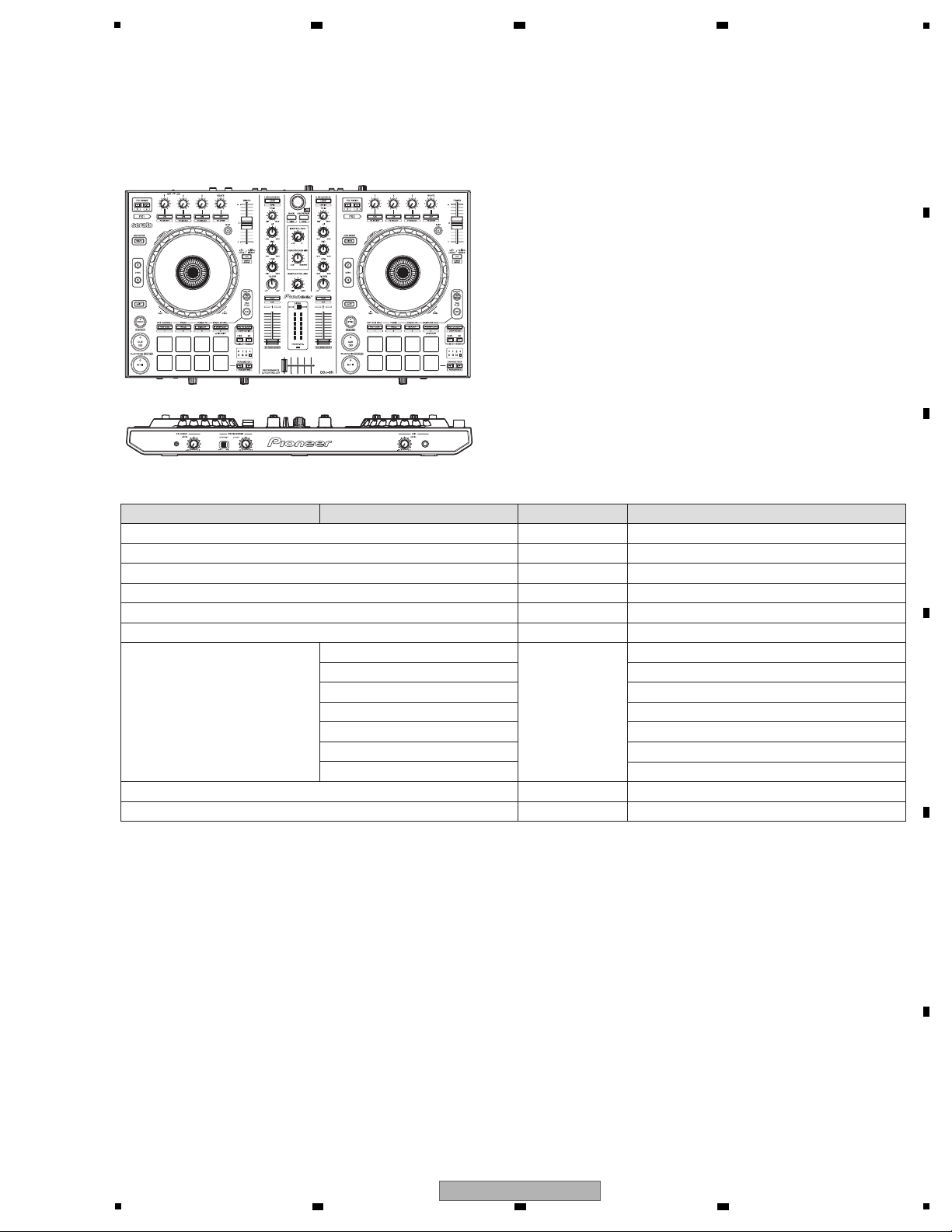
2. SPECIFICATIONS .................................................................................................................................................................5
3. BASIC ITEMS FOR SERVICE...............................................................................................................................................6
3.1 CHECK POINTS AFTER SERVICING............................................................................................................................6
3.2 JIGS LIST .......................................................................................................................................................................6
3.3 PCB LOCATIONS ...........................................................................................................................................................7
4. BLOCK DIAGRAM.................................................................................................................................................................8
D
E
F
4.1 OVERALL WIRING DIAGRAM........................................................................................................................................8
4.2 OVERALL BLOCK DIAGRAM.......................................................................................................................................10
5. DIAGNOSIS.........................................................................................................................................................................12
5.1 TROUBLESHOOTING ..................................................................................................................................................12
5.2 BASIC OPERATION CHECK USING SERATO DJ .......................................................................................................14
6. SERVICE MODE .................................................................................................................................................................17
6.1 SERVICE MODE...........................................................................................................................................................17
7. DISASSEMBLY....................................................................................................................................................................27
8. EACH SETTING AND ADJUSTMENT ................................................................................................................................33
8.1 NECESSARY ITEMS TO BE NOTED...........................................................................................................................33
8.2 UPDATING OF THE FIRMWARE .................................................................................................................................33
8.3 ITEMS FOR WHICH USER SETTINGS ARE AVAILABLE ...........................................................................................35
9. EXPLODED VIEWS AND PARTS LIST...............................................................................................................................38
9.1 PACKING SECTION .....................................................................................................................................................38
9.2 EXTERIOR SECTION...................................................................................................................................................40
10. SCHEMATIC DIAGRAM ....................................................................................................................................................44
10.1 MIC and HEADPHONE PCB ASSYS .........................................................................................................................44
10.2 I/O
10.3 MIXER and CROSS FADER PCB ASSYS..................................................................................................................48
10.4 PANEL-L and R PCB ASSYS......................................................................................................................................50
10.5 WAVEFORMS .............................................................................................................................................................52
11. PCB CONNECTION DIAGRAM ........................................................................................................................................56
11.1 MIC and HEADPHONE PCB ASSYS .........................................................................................................................56
11.2 I/O PCB ASSY ............................................................................................................................................................58
11.3 MIXER and CROSS FADER PCB ASSYS..................................................................................................................60
11.4 PANEL-L and R PCB ASSYS......................................................................................................................................62
12. PCB PARTS LIST ..............................................................................................................................................................64
PCB ASSY ............................................................................................................................................................46
2
1
2 3 4
DDJ-SR
Page 3
5
• For environmental protection, lead-free solder is used on the printed circuit boards mounted in this unit.
Be sure to use lead-free solder and a soldering iron that can meet specifications for use with lead-free solders for repairs
accompanied by reworking of soldering.
• Compared with conventional eutectic solders, lead-free solders have higher melting points, by approximately 40 ºC.
Therefore, for lead-free soldering, the tip temperature of a soldering iron must be set to around 373 ºC in general, although
the temperature depends on the heat capacity of the PC board on which reworking is required and the weight of the tip of
the soldering iron.
Do NOT use a soldering iron whose tip temperature cannot be controlled.
Compared with eutectic solders, lead-free solders have higher bond strengths but slower wetting times and higher melting
temperatures (hard to melt/easy to harden).
The following lead-free solders are available as service parts:
• Parts numbers of lead-free solder:
GYP1006 1.0 in dia.
GYP1007 0.6 in dia.
GYP1008 0.3 in dia.
When you replacing Front panel, JW ring, it is necessary to remove Front panel.
NITTO No. 500
(5 mm × 30 mm)
NITTO No. 500
(5 mm × 40 mm)
When detaching the front panel
The front panel and the Chassis Assy are secured with 10 pieces of double-back tape at the locations shown in the illustration below.
Slowly peel off the tape, taking care that you will not deform the front panel.
When reattaching the front panel
1 Neatly remove any residue of double-back tape from the back of the front panel and the Chassis Assy.
2 Stick 10 pieces (5 mm) of NITTO No. 500 double-back tape to the locations shown in the illustration below then remove the paper liner.
Note: Even if double-back tape was not used in the initial state, be sure to attach double-back tape when reattaching the front panel.
Before securing the front panel to the Chassis Assy with screws, never press on the places where the pieces of double-back tape are
attached.
Press on the places where the pieces of double-bac
k tape are attached after securing the front panel to the Chassis Assy with screws.
Notes:
• Do not reuse the
double-back tape.
• Put the
double-back tape on the Chassis Assy side.
NITTO No. 500
(5 mm × 40 mm)
NITTO No. 500
(5 mm × 80 mm)
Detachment/Reattachment of the front panel
6 7 8
1. SERVICE PRECAUTIONS
1.1 NOTES ON SOLDERING
A
B
1.2 NOTES ON PARTS REPLACEMENT
C
D
E
DDJ-SR
5
6 7 8
F
3
Page 4
1
Four washers have been added to the screw-mounted parts of the Pad & FSR Plate Assy to solve the problem that
a performance pad is only pressed halfway although it is fully pressed. This problem was revealed during production.
This emergency measure will be taken care of in the future, but the exact date when the improved products will be produced is
not determined yet. At least the first 20,000 products will have the added washers.
The initial service parts for the Pad & FSR Plate Assy will also require attachment of washers.
To prevent the washers from not being attached during replacement of the Pad & FSR Plate Assy with the one for service,
the Pad & FSR Plate Assy and the washers are to be enclosed in the same package as a kit.
The part number of the kit for service is GXX1374.
When a new Pad & FSR Plate Assy for service is to be reassembled, be sure to attach the enclosed 4 washers to
the screw-mounted par
ts. (See the figure below.)
Note on Replacement of the Pad & FSR Plate Assy
Pad & FSR Plate Assy
Attach the washer.
This unit will automatically enter Demo mode if it is left unoperated for 10 minutes in Normal Operation mode, and a
demonstration with LED illumination will start.
To cancel this mode, operate any control or button of this unit.
To disable Demo mode, change the setting in the settings of Utilities mode 1. (For details, refer to the operating instructions.)
A
B
2 3 4
C
D
1.3 ABOUT DEMO MODE
E
F
4
1
2 3 4
DDJ-SR
Page 5

5
General – Main Unit
Power supply........................................................................ DC 5 V
Rated current....................................................................... 500 mA
Main unit weight..........................................................4.5 kg (9.9 lb)
Max. dimensions......553.6 mm (W) × 65.3 mm (H) × 319.1 mm (D)
(21.8 in. (W) × 2.6 in. (H) × 12.6 in. (D))
Tolerable operating temperature..............................+5 °C to +35 °C
Tolerable operating humidity............5 % to 85 % (no condensation)
Audio Section
Rated output level
MASTER OUT 1............................................................. 4.2 Vrms
MASTER OUT 2............................................................. 2.1 Vrms
BOOTH........................................................................... 2.1 Vrms
Total harmonic distortion
MASTER OUT..................................................................0.006 %
Frequency characteristic
USB, AUX, MIC ................................................... 20 Hz to 20 kHz
S/N ratio (when playing on computer)
MASTER OUT................................................................... 101 dB
Input impedance
AUX ..................................................................................... 47 kΩ
MIC...................................................................................... 10 kΩ
Output impedance
MASTER OUT....................................................................... 1 kΩ
PHONES ...............................................................................32 Ω
USB AUDIO.................................................... 24 bit/Fs : 44.1 kHz
Input / Output terminals
AUX IN input terminal
RCA pin jacks........................................................................1 set
MIC terminal
Phone jack (Ø 6.3 mm).......................................................... 1 set
BOOTH OUT/MASTER OUT2 output terminal
RCA pin jacks........................................................................1 set
MASTER OUT1 output terminal
Phone jack (Ø 6.3 mm).......................................................... 1 set
PHONES output ter
minal
Stereo phone jack (Ø 6.3 mm) ..............................................1 set
Stereo mini phone jack (Ø 3.5 mm)....................................... 1 set
USB terminal
B type ....................................................................................1 set
• CD-ROM (Installation Disc)
• USB cable
(408-SUB-132)
• Read Before Use (Important)/Quick Start Guide
(DDJ-SR/CKSUVYXE5: 502-DDJSRA-3325A, 502-DDJSRA-3326A)
(DDJ-SR/XECN5: 502-DDJSRB-3327)
• Warranty (for some regions)
The included warranty is for the European region.
• For the North American region, the corresponding information is
provided on the last page of both the English and French
versions of the “Read Before Use (Important)/Quick Start Guide”.
• For the Japanese region, the corresponding information is
provided on the last page of the Japanese version of the “Read
Before Use (Important)/Quick Start Guide”.
Accessories
2. SPECIFICATIONS
6 7 8
A
B
C
D
E
F
DDJ-SR
5
6 7 8
5
Page 6
1
Distortion
Noise
Volume too low
Volume too high
Volume fluctuating
Sound interrupted
See the table below for the items to be checked regarding audio.
No. Procedures
Item to be checked regarding audio
Check points
1 Check the firmware version. The firmware version must be the latest one.
If it is not the latest one, be sure to update it.
Items to be checked after servicing
6 Check the appearance of the product. No scratches or dirt on its appearance after receiving it for service.
To keep the product quality after servicing, confirm recommended check points shown below.
2 Confirm that the customer complaint has been resolved.
If the problem pointed out by the customer occurs with a specific
source or operation, such as PC input, AUX/MIC input, Fader, or
VOL, input that specific source then perform that specific
operation for checking.
The symptoms in question must not be reproduced.
There must be no abnormality in audio signals or operations.
4 Check the analog audio output.
Connect this unit with a PC with the DJ application (Serato DJ)
installed, via USB, then play back audio.
There must be no errors, such as noise, in audio signals and
operations of the MASTER/HEADPHONES outputs.
5 Check the analog audio input.
Input an audio signal via AUX/MIC.
There must be no abnormality in audio signals or operations.
3 Check operations of the operating elements.
Enter Service mode.
There must be no errors in operations of each button, the jog dial,
LEDs, VOL, fader control, and rotary encoder.
Lubricants and Glues List
Name Part No. Remarks
Jigs List
Jig Name Part No. Purpose of use / Remarks
USB cable GGP1193 for PC connection
Adhesive GYL1001 Refer to “7. DISASSEMBLY”.
Grease GEM1096 Refer to “7. DISASSEMBLY”.
2 3 4
3. BASIC ITEMS FOR SERVICE
3.1 CHECK POINTS AFTER SERVICING
A
B
C
D
3.2 JIGS LIST
E
F
6
1
2 3 4
DDJ-SR
Page 7
5
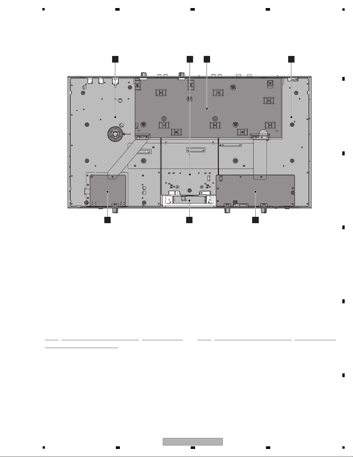
Mark No. Description Part No. Mark No. Description Part No.
LIST OF ASSEMBLIES
NOTES: - Parts marked by “NSP” are generally unavailable because they are not in our Master Spare Parts List.
-
The > mark found on some component parts indicates the importance of the safety factor of the part.
Therefore, when replacing, be sure to use parts of identical designation.
MIC PCB ASSY 704-SR-A601
HEADPHONE PCB ASSY 704-SR-A600
I/O PCB ASSY 704-SR-A596
MIXER PCB ASSY 704-SR-A597
CROSS FADER ASSY 704-DJM250-A032
PANEL-L PCB ASSY 704-SR-A599
PANEL-R PCB ASSY 704-SR-A598
C
I/O
PCB ASSY
G
PA NEL-R
PCB ASSY
D
MIXER
PCB ASSY
F
PA NEL-L
PCB ASSY
E
CROSS FADER
PCB ASSY
B
HEADPHONE
PCB ASSY
A
MIC
PCB ASSY
• Bottom view
3.3 PCB LOCATIONS
6 7 8
A
B
C
D
E
F
DDJ-SR
5
6 7 8
7
Page 8
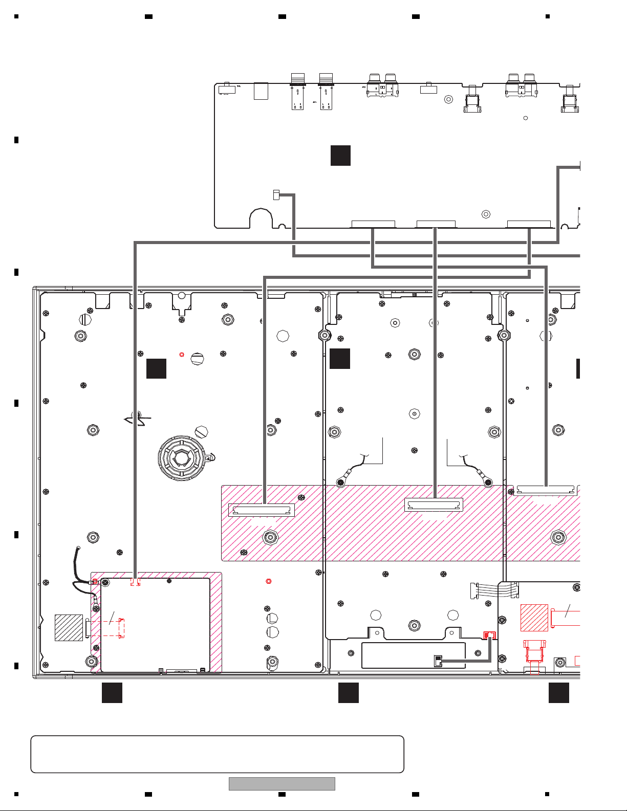
1
W7
CN2C
CN6
CN500
CN1B
CN2B
W
CN2A
CN01
W700
CN701A CN701B
CN1A CN3A
CHASSIS
CHASSIS
CHASSIS
TO
OUTPUT BOARD
TO
CARBON PAD FFC WIRE
TO
CARBO
TO
OUTPUT BOARD
C
I/O PCB ASSY
(704-SR-A596)
A
MIC PCB ASSY
(704-SR-A601)
G
PANEL-R PCB ASSY
(704-SR-A598)
D
MIXER PCB ASSY
(704-SR-A597)
P
(
E
CROSS FADER PCB ASSY
(704-DJM250-A032)
B
H
(7
1
2
3
4
-
When ordering service parts, be sure to refer to "EXPLODED VIEWS and PARTS LIST" or "PCB PARTS LIST".
-
The > mark found on some component parts indicates the impor tance of the safety factor of the part.
Therefore, when replacing, be sure to use parts of identical designation.
2 3 4
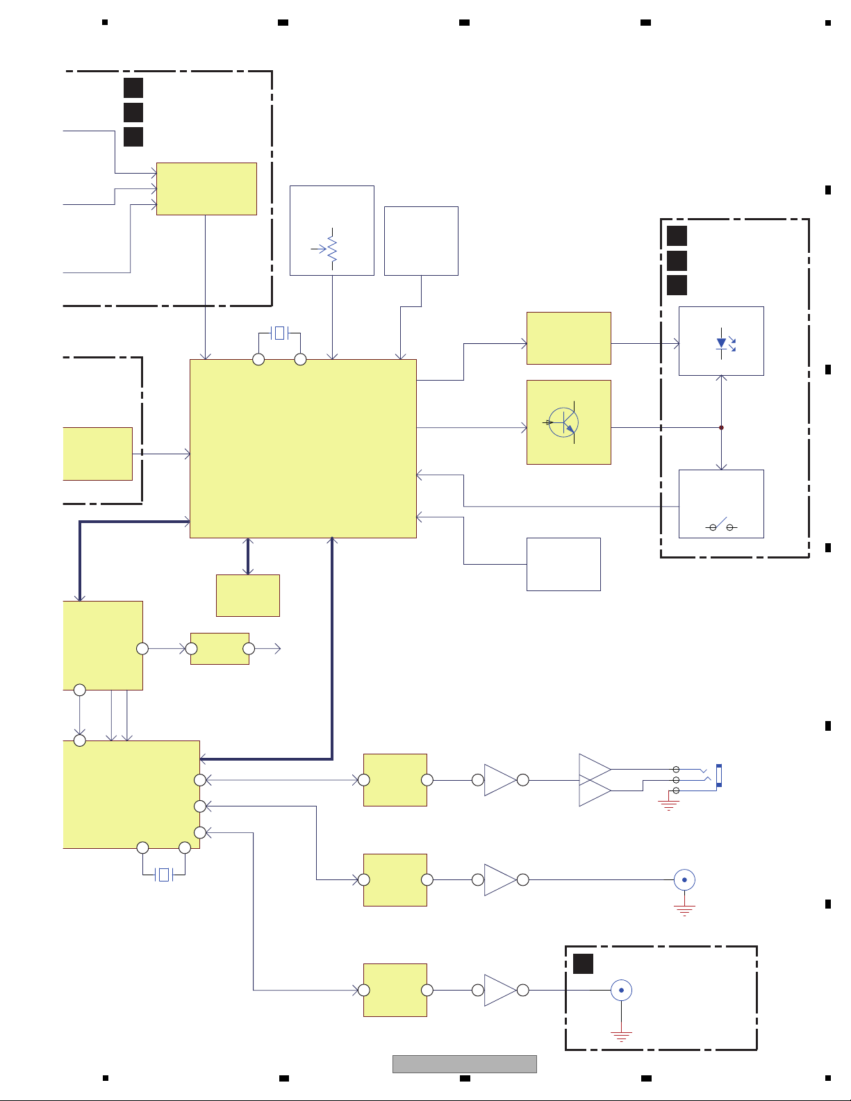
4. BLOCK DIAGRAM
4.1 OVERALL WIRING DIAGRAM
A
B
C
D
E
F
8
1
2 3 4
DDJ-SR
Page 9
CN500
CN2B
W6
CN701B
CN7
CN3A
CHASSIS
TO
CARBON PAD FFC WIRE
F
PANEL-L PCB ASSY
(704-SR-A599)
B
HEADPHONE PCB ASSY
(704-SR-A600)
1
2
3
4
5
6
7
8
9
10
11
12
13
14
15
16
17
18
19
20
21
22
23
24
25
26
27
28
29
30
31
32
33
34
CN2C
LED6
LED7
LED8
KEY1
KEY3
KEY2
AD3.3V
ADGND
S1
LED- G
WL -B
S4
S3
S2
LED2
LED1
D3.3V
LED5
LED4
LED3
KEY4
KEY5
WL -A
B
A
AD9
AD8
AD6b
AD12
S5
S6
C
D5V
DGND
(AD7b)
(AD13)
(AD14)
1
2
3
4
5
6
7
8
9
10
11
12
13
14
15
16
17
18
19
20
21
22
23
24
25
26
27
28
29
30
31
32
33
34
CN2B
LE
D6
LED7
LED8
KEY1
KEY3
KEY2
AD3.3V
ADGND
S1
LED- G
WL -B
S4
S3
S2
LED2
LED1
D3.3V
LED5
LED4
LED3
KEY4
KEY5
WL -A
B
A
AD9
AD8
AD6b
(WR- A)
(WR- B)
AD12
S5
S6
C
(AD15)
D5V
DGND
1
2
3
4
5
6
7
8
9
10
11
12
13
14
15
16
17
18
19
20
21
22
23
24
25
26
27
28
29
30
31
32
33
34
CN3A
LED6
LED7
LED8
KEY1
KEY3
KEY2
AD3.3V
ADGND
S10
WR- B
S13
S12
S11
LED2
LED1
D3.3V
LED5
LED4
LED3
KEY4
KEY5
WR- A
B
A
AD14
AD13
AD7b
AD15
S14
S15
C
D5V
LE
D-G
DGND
1
2
3
4
5
6
7
8
9
10
11
12
13
14
15
16
17
18
19
20
21
22
23
24
25
26
27
28
29
30
31
32
33
34
CN2A
LED6
LED7
LED8
KEY1
KEY3
KEY2
AD3.3V
ADGND
S1
WL -B
S4
S3
S2
LED2
LED1
D3.3V
LED5
LED4
LED3
KEY4
KEY5
WL -A
B
A
AD9
AD8
AD6b
AD12
S5
S6
C
D5V
LED- G
DGND
1
2
3
4
5
6
7
8
9
10
11
12
13
14
15
16
17
18
19
20
21
22
23
24
25
26
27
28
29
30
CN1A
ADGND
C
AD11
AD1
AD0
AD3
AD2
KE
Y3
S8
LED8
LED7
LED6
LED5
LED4
LED3
KEY2
LED1
LED2
ENCA
ENCB
A
B
AD3.3V
S9
S7
KEY1
D3.3V
D5V
LED- G
DGND
1
2
3
4
5
6
7
8
9
10
11
12
13
14
15
16
17
18
19
20
21
22
23
24
25
26
27
28
29
30
CN1B
ADGND
LED- G
C
AD11
AD1
AD0
AD3
AD2
KEY3
S8
LED8
LED7
LED6
LED5
LED4
LED3
KEY2
LED1
LED2
ENCA
ENCB
A
B
AD3.3V
S9
S7
KEY1
D3.3V
D5V
DGND
AD3.3V
1
2
3
4
5
CN701B
REV
CURVE
HPVR
ADGND
1
2
3
4
5
CN701A AD3.3V
REV
HPVR
ADGND
CURVE
D
MIXER
PCB ASSY
C
I/O
PCB ASSY
B
HEADPHONE
PCB ASSY
D
MIXER
PCB ASSY
1
2
G
PANEL-R
PCB ASSY
C
I/O
PCB ASSY
3
C
I/O
PCB ASSY
F
PANEL-L
PCB ASSY
4
4
5
6 7 8
A
B
C
D
E
F
DDJ-SR
5
6 7 8
9
Page 10
1
AD * 8
AD * 8
FSR PAD * 8
RIGHT
FSR PAD * 8
LEFT
AD Expansion
AD Port 4 TO 16
74HC4052 * 2
ROTATE VR * 23
ADSP-BF592
(I2S format for audio data)
(44.1K/24bit/512fs for A/D,D
24
AUX
MIC
USB PortB
TUSB3200
PCI-0
PCO-0
PCO-1
BCK
LRCK
6M
(12MHz or 48MHz)
VUSB
TEMPO VR * 2
SLIDER SW * 1
AD * 1
AD * 4
AD * 23
I2C
IC11
IC10
IC27
IC13
IC9
IC900IC900
IC3
IC23
IC22
IC1
IC2
IC15
X1
IC16
IC502
C
I/O PCB ASSY
D
M
A
MIC PCB ASSY
F
PANEL-L PCB ASSY
G
PANEL-R PCB ASSY
F
P
G
P
D5V D3.3V
BD12AK5FB
D1.2V
12
TPS54232
INVERTER
-6V
TPS61085
BOOST
6V
5V
BA05
A5V AD5V
A3.3V
VUSB
TPS54232
STEP DOWN
DA3.3V
ADC
PCM1803
-5.46dB
AUX
ADC
PCM1803
MIC
+20dB
L
3
G
1
S
4
LEVEL0dB
-5.46dB
LEVEL
+9.4dB
44
50
51
39
37
3
3 5 1
5 7
1
1
3 1 1 12
1 12
31
61
32
64 63
36 38
2 3 4
4.2 OVERALL BLOCK DIAGRAM
A
B
C
D
E
F
10
DDJ-SR
1
2 3 4
Page 11
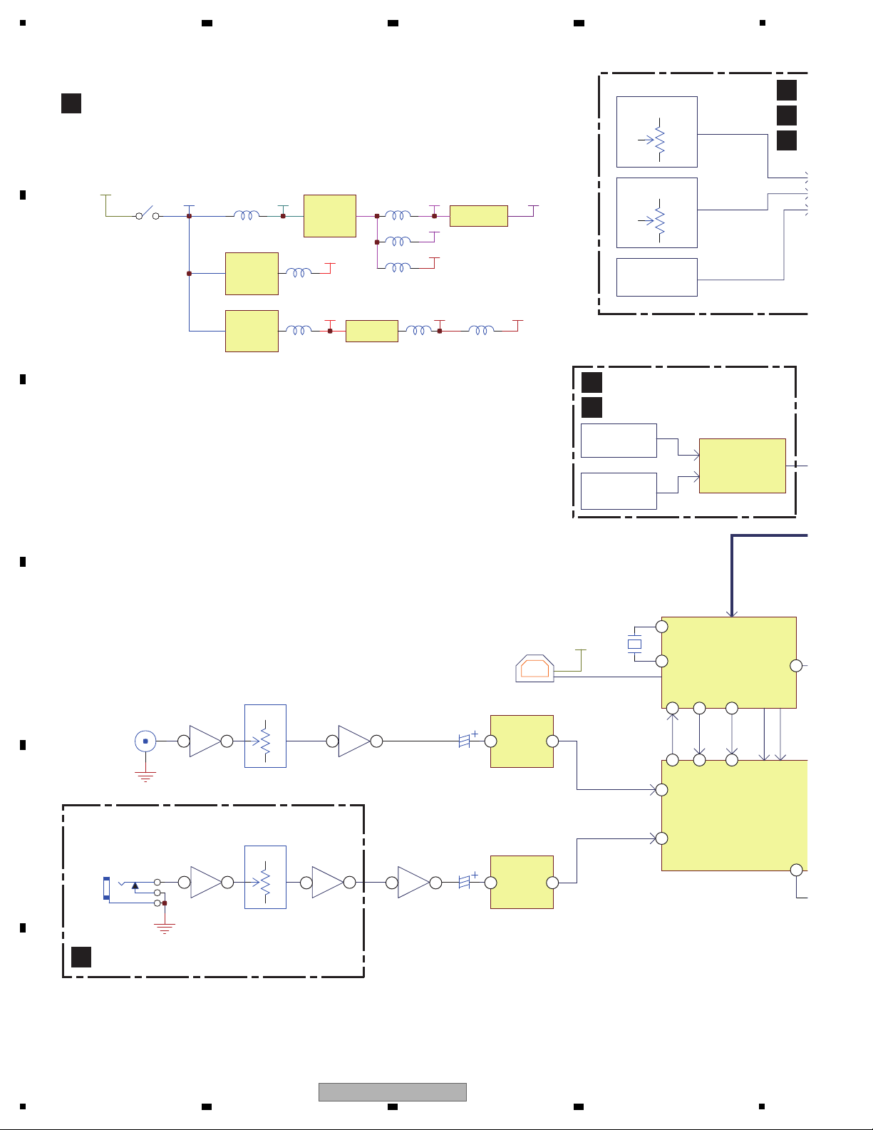
8M
MKL15Z128VLK4
(24MHz )
32Bit MCU
AD * 4
ENCODE * 1
AD Expansion
74HC4052 * 2
EEPROM
24LC02BT
I2C1
CH FADER * 2
AD Expansion
AD Port 4 TO 32
74HC4051 * 4
Buffer
74HCT244 * 1
LED * 101 + 22 PCS
GPIO * 8
GPIO * 15
GPIO * 7
DATA * 8
SCAN * 15
GPIO * 5(KEY)
12
TACT SW * 58
SLIDER SW * 1
ENCODE SW * 1
CROSS FADER * 1
ADSP-BF592
24.576M
PCO-1
BCK
LRCK
SPI
MCLK
SN74LVC1G
SCHMITT
SCK
AD/DA CLK
JOG WHEEL *2
SLIDER SW * 1
BOOTH VR * 1
JOG TOUCH * 2
AD * 1
AD * 4
AD * 4
AD * 4 AD * 2
AD * 23
LPF&.
LPF&.
LPF&.
BOOTH/MASTER2
(RCA)
NJM4580
NJM4556
MAS
HP
Headphone
(32 ohm/6.3mm & 3.5mm)
DAC
CS4344
DAC
CS4344
DAC
CS4344
NJM4580
NJM4580
L
3
R
2
G
1
MASTER1
BOOTH
Text
SD1757 * 15
Buffer
IC15
X2
X3
IC16
IC18
IC19
IC20
IC502
IC500, IC700, IC701
IC21
IC7
IC5
IC4
IC6
IC26
IC24
IC25
D
MIXER PCB ASSY
B
HEADPHONE PCB ASSY
Y
F
PANEL-L PCB ASSY
G
PANEL-R PCB ASSY
D
MIXER PCB ASSY
F
PANEL-L PCB ASSY
G
PANEL-R PCB ASSY
40 41
2344
36
5
1 7 6 7
1 7 6 7
1 7 2 1
4
61 62
63
38
5
6 7 8
A
B
C
D
5
DDJ-SR
6 7 8
E
F
11
Page 12
1
[0] Service mode
[1] Troubles of starting system and
communication
[2] Troubles of operation element
and LED
Conduct diagonosis on troubles using Service mode.
Does the MIDI
command output?
Is VUSB 5 V?
Does D3.3V become
3.3 V correctly?
Does oscillator (X3)
oscillate it? (8 MHz)
When you turn VR,
does the signal from VR
change?
Confirm input signal A,B,C.
Is the signal H or L?
When you turn VR,
does the output signal of
IC700, 701 change?
No
No
No
Ye s
Ye s
Ye s
Ye s
Ye s
Ye s
Check power switch turn on.
Confirm if the USB cable is
connected properly.
USB cable is defective.
Replace the USB cable.
No
Confirm that ON does SW, and
both ends do conduction.
When SW does not do conduction,
replace the SW.
No
X3 is defective.
Replace the X3.
No
UCOM (IC20) is defective.
Replace the I/O PCB Assy.
No
VR is defective.
Replace the corresponding part.
No
Analog SW (IC700, 701) is
defective.
Replace the MIXER PCB Assy.
UCOM (IC20) is start-up
abnormality.
Ye s
Confirm analog SW where
a signal is connected to.
Ye s
Confirm whether a matrix circuit
is defective.
No
The power is turned on correctly,
there is a problem with the LED
circuit. See "LED does not lit"
UCOM (IC20) is defective.
Replace the I/O PCB Assy.
Power supply IC (IC27) is defective.
Replace the I/O PCB Assy.
Ye s
UCOM (IC20) is defective.
Replace the I/O PCB Assy.
Ye s
UCOM (IC20) is defective.
Replace the I/O PCB Assy.
Ye s
Q500 to 505, 700 to 702 are
defective.
Replace the corresponding part.
The power is not turned on.
Is the buttons which does
not work the plural?
When you pressed on button,
is the target KEY signal "H"?
Buttons reads it in a matrix.
Buttons or slide SW does not work.
Rotary VR does not work.
Ye s
No
UCOM (IC16) is defective.
Replace the I/O PCB Assy.
No
UCOM (IC16) is defective.
Replace the I/O PCB Assy.
Ye s
Replace the corresponding part.
Is the communication line
of the USB "H" or "L"?
Is the abnormality in
the parts mentioned above?
Confirm whether a USB cable is
connected properly.
Confirm whether there is not the
part on the USB line abnormally.
Object: D11 - 14, L13
Cannot communicate USB.
Do not push and rotary
which work?
Check on 3 pin, 1 pin of
the rotary selector.
When you turned a rotary
selector, is the signal H?
See "Buttons or slide SW does
not work".
Push
Rotary
No
UCOM (IC20) is defective.
Replace the I/O PCB Assy.
Ye s
Rotary selector is defective.
Replace the rotary selector.
Rotary selector does not work.
5. DIAGNOSIS
5.1 TROUBLESHOOTING
A
2 3 4
B
C
D
E
F
12
1
DDJ-SR
2 3 4
Page 13
5
[3] Troubles of settings
Ye s
UCOM (IC20) is defective.
Replace the I/O PCB Assy.
Ye s
UCOM (IC20) is defective.
Replace the I/O PCB Assy.
Ye s
Damage of the LED.
Replace the LED.
Confirm whether each cables is
connected properly.
When you pressed Pad,
does the voltage change
with CN500 pins 2 - 9?
When you touched Jog,
does the voltage change
with IC501 pin 5?
When you turned Jog,
does the voltage change
with IC20?
When you pressed Pad,
does the voltage change
by the output of IC502?
No
FSR PCB is defective.
Replace the FSR Plate Assy L, R.
No
IC502 is defective. Replace the
PA NEL L or R PCB Assy.
No
LED DRIVER (IC21) is defective.
Replace the I/O PCB Assy.
No
IC16 is defective.
Replace the I/O PCB Assy.
No
The abnormality of the IC which
LED is connected to if you confirm
that all keys work normally and do
not have any problem.
Replace the I/O PCB Assy.
Ye s
Pad does not work.
The LED lits by matrix drive.
Does not all LED lit?
Does not only
one LED lit?
Is the signal of "DATA1 - 8"
of the LED control signal "L"?
Ye s
LED does not lit.
No
Ye s
UCOM (IC20) is defective.
Replace the I/O PCB Assy.
No
E2ROM (IC19) is defective.
Replace the I/O PCB Assy.
The setting information is saved
in IC19.
Are SCL and the SDA
signals "H" or "L"?
Cannot store user settings.
[4] Troubles of Jog touch and Jog rotation
Ye s
UCOM (IC20) is defective.
Replace the I/O PCB Assy.
No
IC501 is defective. Replace the
PA NEL-L or R PCB Assy.
No
UCOM (IC20) is defective.
Replace the I/O PCB Assy.
Confirm whether each cables is
connected properly.
Jog touch and Jog rotation does
not work.
[5] Troubles of sound input and output
Sound does not output.
Ye s
Confirm if the USB cable is
connected properly.
Ye s
Ye s
Sound signal does not have
abnormality, or confirm the
following part.
IC23 to 26 (A/D and D/A IC)
Does USB input signal
output it from pins 2
and 3 of JK1?
Ye s
Are the data control signals
in pins 34, 35 and 44
of IC16?
No
USB cable is defective.
Replace the USB cable.
No
A/D and D/A IC are defective.
Replace the I/O PCB Assy.
Is the abnormality in
the parts mentioned above?
6 7 8
A
B
C
D
E
5
DDJ-SR
6 7 8
F
13
Page 14
1
[Installation of Serato DJ]
[Connections]
[Operating procedures]
A brief explanation of how to install Serato DJ on a PC is given below. For details, refer to the operating instructions of the
software.
If the OS of the PC to be used is Windows, install the driver software that enables audio output from the PC beforehand.
The operating environment of the PC required for installation of Serato DJ is shown below.
• For the latest information on the required operating environment and compatibility as well as to acquire the latest operating
system, refer to “Software Info” under “DDJ-SR” on the Pioneer DJ support site below.
http://pioneerdj.com/support/
• Operating System support assumes you are using the latest point release for that version.
For the latest version of the Serato DJ software, access Serato.com and download the software from there.
For downloading, registration of a user account at "Serato.com" is required.
Unzip the downloaded file, then double-click the unzipped file to launch the installer.
Read the terms of the license agreement carefully
, and if you agree, select [I agree to the license terms and conditions],
then click [Install].
After installation is completed, the Installation Completed screen will be displayed. Click on [Close] to terminate the Serato DJ
installer.
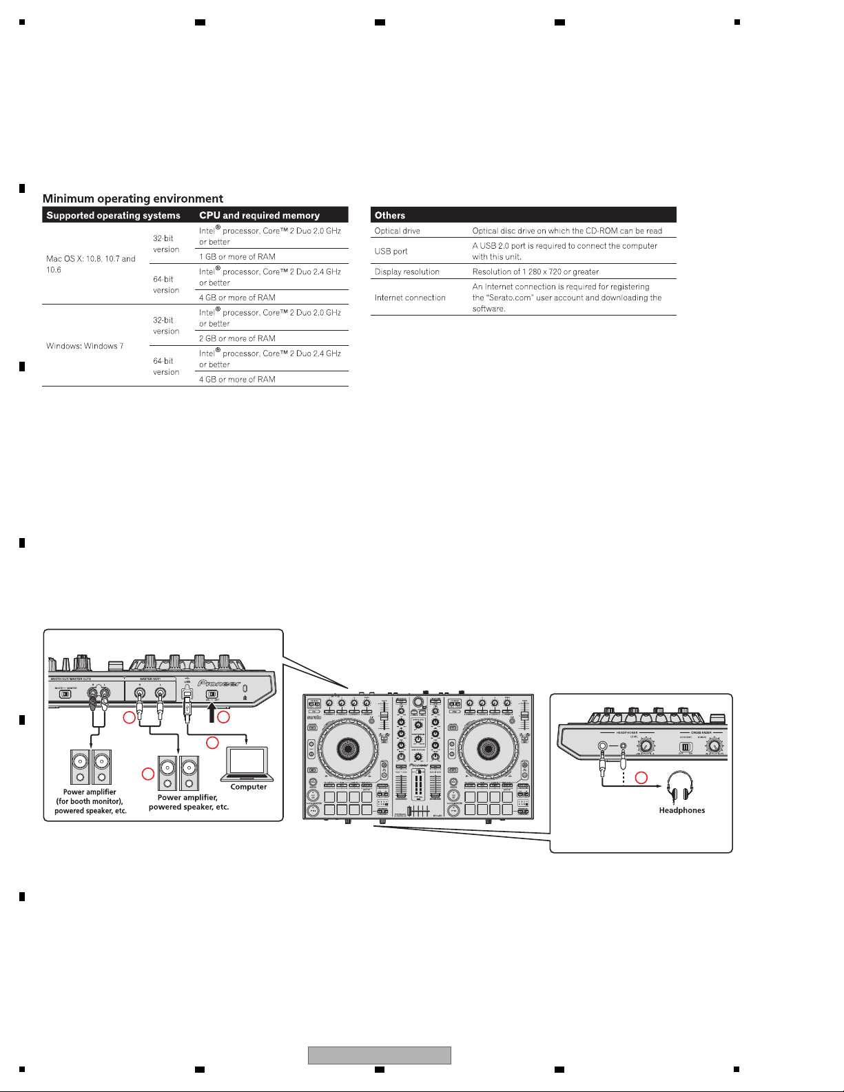
1 Connect headphones to one of the [HEADPHONES] terminals.
2 Connect powered speakers, a power amplifier, components, etc., to the [MASTER OUT 1] or
[BOOTH OUT/MASTER OUT 2] terminals.
3 Connect this unit to your computer via a USB cable.
4 Turn on the computer’ s power.
5 Switch the [ON/OFF] switch on this unit’ s rear panel to the [ON] side to turn this unit’ s power on.
6 Turn on the power of the devices connected to the output terminals (powered speakers, power amplifier, components, etc.).
1
2
3
5
6
2 3 4
5.2 BASIC OPERATION CHECK USING SERATO DJ
A
B
C
D
E
F
14
DDJ-SR
1
2 3 4
Page 15
5
Starting the system
Launching Serato DJ
From the Windows [Start] menu, click the [Serato DJ] icon under [All Programs] > [Serato] > [Serato DJ].
When Serato DJ is launched after it is installed, a yellow icon saying “BUY/ACTIVATE” might be displayed in the License panel
on the right side of the Serato DJ screen.
DDJ-SR users do not have to activate or buy Serato DJ.
If you tick the check box of [DO NOT SHOW AGAIN] and click [Online], the icon will disappear thereafter.
Importing tracks
1 Click the [Files] key on the Serato DJ software screen to open the [Files] panel.
2 Click the folder on the [Files] panel containing the tracks you want to add to the library to select it.
3 On the Serato DJ software screen, drag and drop the selected folder to the crates panel.
Loading tracks and playing them
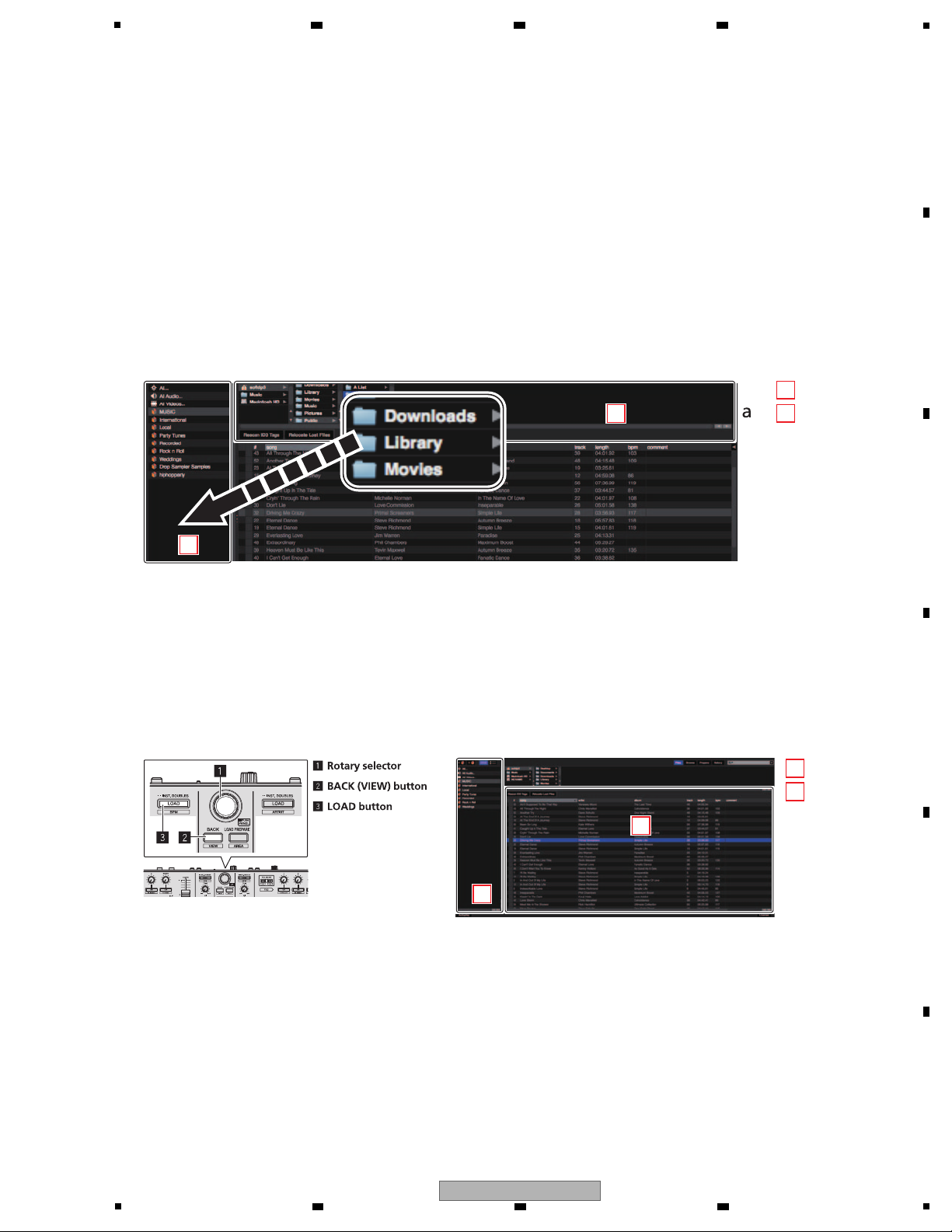
1 Press this unit’ s [BACK (VIEW)] button, move the cursor to the crates panel on the computer’ s screen, then turn the
rotary selector to select the crate, etc.
2 Press the rotary selector, move the cursor to the library on the computer’ s screen, then turn the rotary selector and
select the track.
3 Press the [LOAD] button to load the selected track onto the deck.
: [Files] panel
b
a
a
: Crates panel
b
: Library
a
: Crates panel
b
b
a
6 7 8
A
B
C
D
E
F
DDJ-SR
5
6 7 8
15
Page 16
1
Playing tracks and outputting the sound
1 Set the positions of the controls, etc., as shown below.
2 Press the [f] button to play the track.
3 Move the channel fader away from you.
4 Turn the [TRIM] control.
Adjust [TRIM] so that the orange indicator on the
channel level indicator lights at the peak level.
5 Turn the [MASTER LEVEL] control to adjust the audio
level of the speakers.
Monitoring sound with headphones
Set the positions of the controls, etc., as shown below.
1
1
10
3
2
2
3
4
5
6
7
8
9
10
11
11
2
4 4
5
6
9
6
3
7
8
A
2 3 4
B
C
D
E
F
16
DDJ-SR
1
2 3 4
Page 17
5
[1] Error Alarming
If unusual detection is occurred during Power on or working, Indicate notice by LED.
Error LED Remarks
1
Abnormalities in
FLASH-ROM of MAIN_UCOM
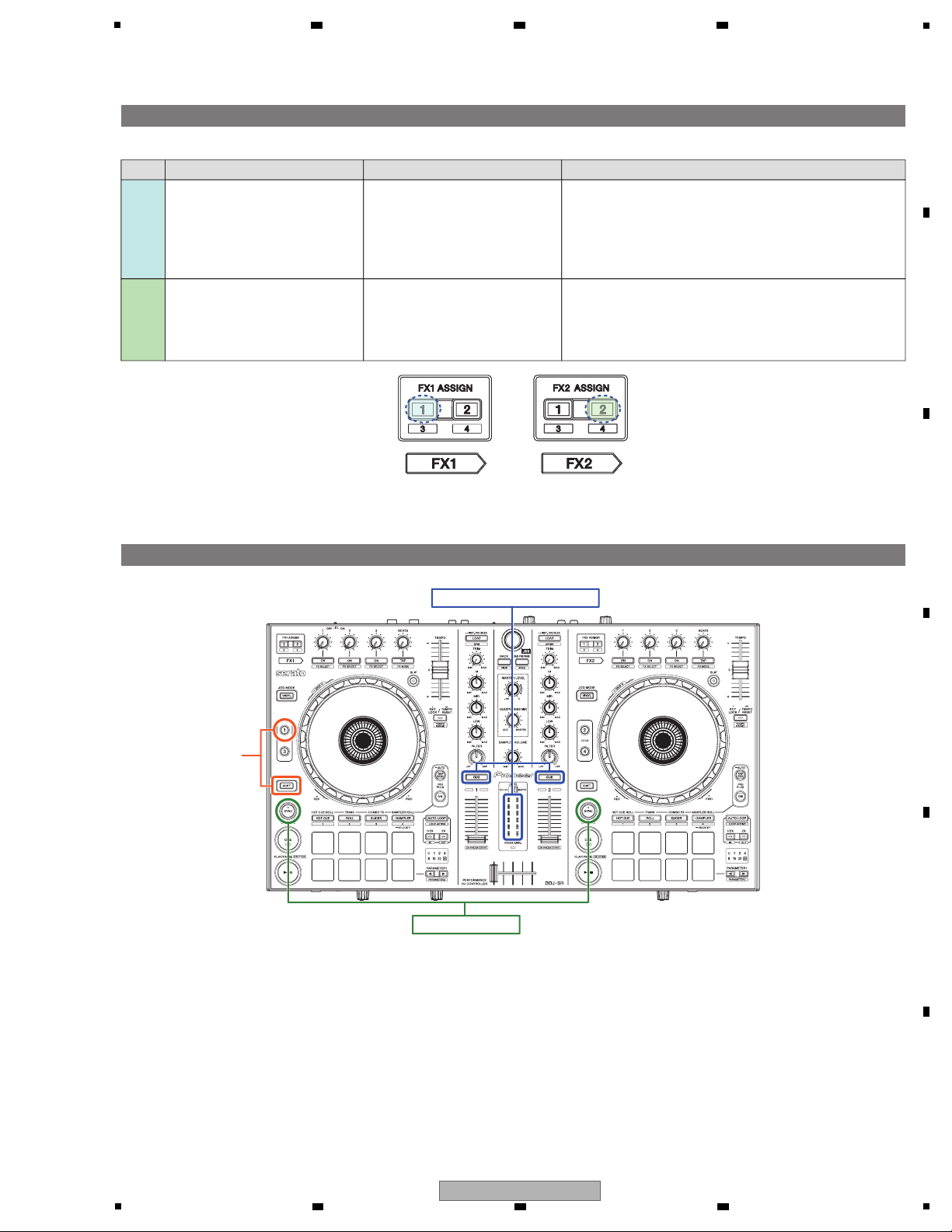
The "FX1 Assign" LED of Deck1
Blinks in a cycle of 1 second.
When update goes wrong and FLASH-ROM is not written
correctly, it will be in this state.
If the last update failured, the LED blinks when next Power-on.
Perform updating again. If this error warning persists, replace
the USB cable. If this error warning persists more, replace the
I/O PCB Assy.
2 Abnormalities of USB controller The "FX2 Assign" LED of Deck4
Blinks in a cycle of 1 second.
When the time when it cannot communicate with USB
controller correctly although USB cable is connected at the
time of starting, it will be in this state.
Replace the USB cable. If this error warning persists, replace
the I/O PCB Assy.
1
2
[2] Service mode
Press and hold the left DECK "SHIFT" button and the left "DECK 1" button, then Power-ON.
The firmware version is displayed first. LED except it turn off.
[Method to enter]
Power-OFF
[Method to exit]
When in this mode, the firmware version display appear first.
In this mode, it does not work to communicate with computer via USB.
In this mode, LED dimmer is not available.
[Note]
into
Service mode
Firmware version (x.xx)
Factory Reset
6 7 8
6. SERVICE MODE
6.1 SERVICE MODE
A
B
C
D
E
5
6 7 8
DDJ-SR
F
17
Page 18
1
The format of the firmware version is "x.xx". (x: decimal)
It is displayed by the Headphone CUE/TAP buttons (Deck1 / Deck 2) and Level indicator.
The firmware display the three-digit every 2 seconds in three times.
The digits express by Headphone CUE/TAP buttons, and the numbers express by Level Indicator.
1. Check of the Firmware Version
2 seconds later
[Numerics expressed with the number of lit LEDs]
0123456789
X.XX X.XX X.XX
2 seconds later 2 seconds later
A
2 3 4
B
C
D
E
F
18
1
2 3 4
DDJ-SR
Page 19
5
In case of the left parts, the left parts LED are lit.
In case of the right parts, the right parts LED are lit.
In case of the center parts, the right&left parts LED are lit.
All buttons other than the Rotary selector, LED will light only while it is pressed.
[Note]
LED lighting specification for parts type
After checking the firmware version, you can check if each UI parts (button/jog dial/knob/fader etc.) are not abnormal.
All UI parts of top&front panel are objects to check.
2. Check of UI parts & LED
Parts type UI Parts Name Function LED to check
Push switches (with LED)
Rotary selector
Press Own LED
Turn All LED (*7)
Jog dial (rotate operation) Turn "Level indicator" LED (*1)
Volume knob, TEMPO slider Turn "Level indicator" LED (*2)
Channel fader Slide "Level indicator" LED (*3)
Cross fader Slide "Beat indicator" LED (*4)
CROSS FADER REVERSE switch Slide "CROSS F. REV. indicator" LED (*5)
Level indicator switch Slide "Level indicator" LED (*1)
Push switches (without LED)
Rotary selector
BACK (VIEW) button
LOAD PREPARE (AREA) button
Jog dial (touch operation) (Deck 1)
Jog dial (touch operation) (Deck 2)
SHIFT button (Deck 1)
SHIFT button (Deck 2)
Press
All LED (*6)
"Headphones CUE/TAP button" LED (Deck 1)
"Headphones CUE/TAP button" LED (Deck 2)
Level indicator left side
Level indicator right side
"HOT CUE" LED (Deck 1)
"HOT CUE" LED (Deck 2)
6 7 8
A
B
C
D
E
F
DDJ-SR
5
6 7 8
19
Page 20
1
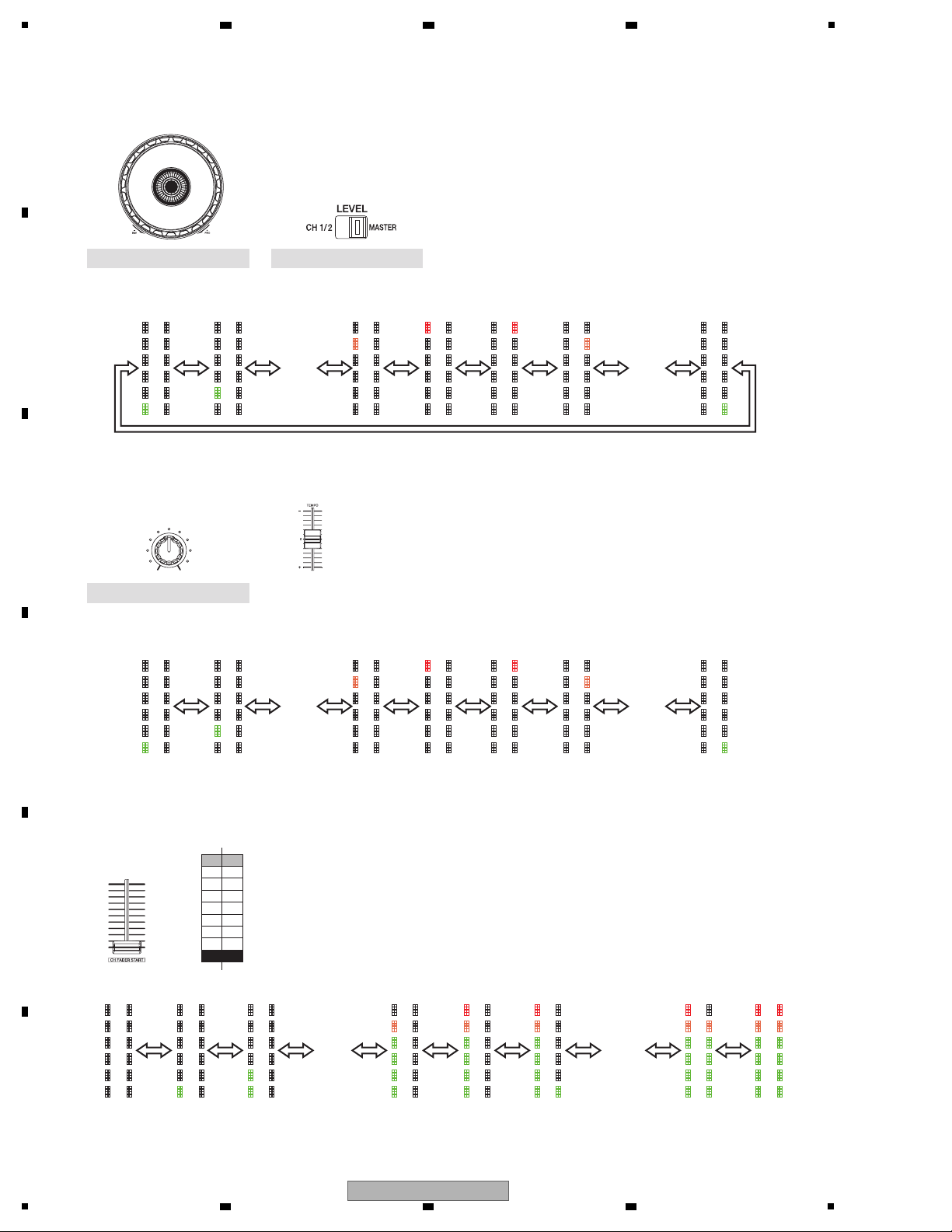
In these type, the position is indicated in 12 steps from minimum to maximum.
In channel fader, the position is indicated in 13 steps from minimum to maximum.
MIN
MAX
MAX
MAX
MIN
MIN
(*2) Volume knob, TEMPO slider
(*3) Channel fader
The starting position depends on the last position.
Jog dial
Volume type
Level indicator switch
(*1) Jog dial (Rotate operation), Level indicator switch
1 2 5 6 7 8
• • •
12
• • •
1 2 5 6 7 8
• • •
12
• • •
1 2 3 6 7 8
• • •
12 13
• • •
A
2 3 4
B
C
D
E
F
20
1
DDJ-SR
2 3 4
Page 21

5
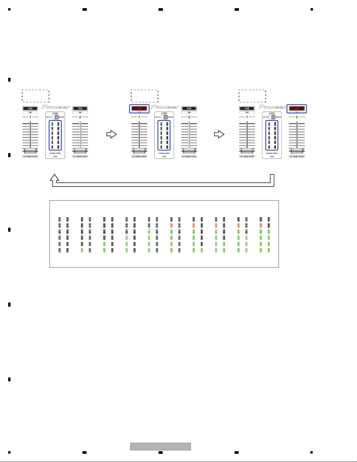
In Crossfader, the position is indicated in 9 steps from minimum to maximum.
Mode: LED BRIGHTNESS Mode
When Rotary selector is pressed,"LED BRIGHTNESS Mode" is changed cyclically as follows.
• • • → A → B → C → D → A → • • •
When Rotary selector is pressed, "LIGHTING COLOR Mode" does not change.
(*4) Cross fader
OFF ON
MIN MAX
(*5) CROSS FADER REVERSE switch
(*6) Press the Rotary selector
Mode All LED
A FULL BRIGHTNESS: 100 %
B MID BRIGHTNESS: 20 %
CLOW BRIGHTNESS: 10 %
D OFF
Mode: LIGHTING COLOR Mode
(Each mode is indicated with the combination of lighting colors of the LOAD button and the HOT CUE, ROLL, SLICER,
and SAMPLER buttons.)
*As two LEDs of different colors each are embedded in the LOAD button and the HOT CUE, ROLL, SLICER, and
SAMPLER buttons, LIGHTING COLOR mode can be used for failure diagnosis of each LED.
When Rotary selector is rotated clockwise,"LIGHTING COLOR Mode" is changed cyclically as follows.
• • • → 1 → 2 → 3 → 4 → 5 → 1 →• • •
When Rotary selector is rotated counterclockwise,"LIGHTING COLOR Mode" is changed cyclically as follows.
• • • → 5 → 4 → 3 → 2 → 1 → 5 →• • •
When Rotary selectoris rotated, "LED BRIGHTNESS Mode" does not change.
(*7) Rotate the Rotary selector
Mode
LIGHTING COLOR of LED
LOAD
HOT CUE, ROLL,
SLICER, SAMPLER
1 RED & AMBER
2 AMBER
3 AMBER
4 RED
5 RED
BLUE & RED
BLUE
RED
BLUE
RED
• • • • • •
123 5 6 89
MIN MAX
Other LEDs
State of (*6) retained
6 7 8
A
B
C
D
5
6 7 8
DDJ-SR
E
F
21
Page 22

1
into
Measurement mode
Jog dial Rotation Time measurement mode
Volume value fluctuation check mode
[3] Measurement mode
This is the mode to measure jog dial rotation time and the fluctuation of knobs/faders.
(1) Jog dial Rotation Time measurement mode
(2) Volume value fluctuation check mode
Press and hold the "SHIFT"+"DECK3" buttons then Power-ON.
During this mode, "DECK 3" and "DECK 4" LEDs are lit.
[Method to enter]
Power-OFF
[Method to exit]
The following data is reset to the factory default settings by "Factory reset" operation.
• Setting data in Utility mode
• Last memory of users
3. Factory Reset
Press and hold the left DECK "SYNC" button and the right DECK "SYNC" button.
Then factory reset starts and "SYNC"LEDs are lit.
After completing reset, "SYNC" LEDs are turned off.
[Method to reset]
A
2 3 4
B
C
D
E
F
22
1
2 3 4
DDJ-SR
Page 23

5
This is the mode to measure the JOG rotation time which is specified at "Jog dial Performance specification".
The specified range is 100 ± 40 msec.
(1) Jog dial Rotation Time measurement mode
1 Yo u spin Jog dial more than 33*7 = 231 rpm.
*1 In case of less than 231 rpm, it is failure. Then "SLIP" LED (Deck1) is lit.
*2 You must measure by either clockwize or counterclockwize.
2 The controller measures "T1".
*T1: The time that Jog dial rotation speed slow down from 100 rpm to 50 rpm.
3 The controller display result with three Channel level indicators. Refer to below.
The format of the result is "XXX" msec. (X: 0-999 msec .decimal)
It is displayed by the Headphone CUE/TAP buttons (Deck1 / Deck 2) and Level indicator.
Display of the 1st digit Display of the 2nd digit Display of the 3rd digit
[Method to measure]
XXX XXX XXX
[Numerics expressed with the number of lit LEDs]
0123456789
If the measurement result is outside the specified range, check the amount of grease for the Jog dial and the chassis.
6 7 8
A
B
C
D
E
DDJ-SR
5
6 7 8
F
23
Page 24

1
11 2 3 4
1515
1212
1313
1414
2222 2323 2424 2525
5 2626
6
7
8 9 1010 1717 1818 1919 2020
1616
2121
1111
Test subjects to move by turning right / left-turn Rotary selector.
A/D conversion value observation start/reset by push the Rotary selector.
Will be tested fluctuation of voltage (A/D conversion value) which is made each Fader and Rotary volume by Level indicator.
[Overview]
Knobs under test operation are filled blue as below.
[Knobs under test operation]
• For failure judgment of the rotary VRs
As a guide, amplitude values higher than +4 or lower than -4 may be judged as failure.
The VRs can be set to any position during measurement. Possible symptoms are shown below.
• The volume changes arbitrarily.
• Interrupted sound leakage occurs even if the volume is decreased to the minimum at the Master or Booth Monitor.
• The MIDI signal is output even if the corresponding VR is not operated.
• For operation check of a rotary VR after replacement
[Use of this mode during repair]
(2) Volume value fluctuation check mode
1 Choose the test subject by turn left and right Rotary selector.
The LED is lit with the following turns every 1 click.
Turn right: 1 → 2 → 3 → 4 → . . . . . → 25 → 26 → 1 → . . .
Turn left: 26 → 25 → 24 → . . . . . → 2 → 1 → 26 → . . .
Note: Regarding No.15, both LED are lit.
2 Yo u can see what knob/fader is selected by Lighting LED on each button as shown in the above figure.
For example ,LED to test Channel fader is "Headphone CUE/TAP" button's LED.
3 When targeted knob is decided, push the Rotary selector and start observation of A/D conversion value.
Get the A / D conversion value immediately after the start. It will be reference value.
*A/D conversion value to be monitored is Raw data.
4
Start monitoring and later to monitor the A/D conversion value, do the following actions depending on its value with
Master level indicator.
[Test detail]
A
2 3 4
B
C
D
E
F
24
1
2 3 4
DDJ-SR
Page 25

5
1 2 3 4 5 6 7 8 910
* Keep the lighting position at the time of maximum fluctuation of each of the positive & negative direction
Level indicator
5 By pushing the Rotary selector while monitoring the conversion value A/D, it is possible to reset the state of the fluctuations
of the past.
Ex.)
1. Turn EQ HI knob (for DECK 1) to the position you want to
measure.
7. More time has elapsed, Level indicator is lit as
follows: become the value 758 of the A/D.
8. More time has elapsed, To maintain the above display
759 even though the value of the A/D.
9. More time has elapsed, Level indicator is lit as
follows: become the value 757 of the A/D.
10. Off all the LED on Level indicator When you push
the Rotary selector, and this value will be new reference
value.
2. Turn the Rotary selector until the 7th LED (Performance
pad) lights.
3. Start A/D conversion value monitoring to push Rotary
selector. If A/D value of push the Rotary selector is 760,
to monitor the amount of change in the value of A/D as
a reference value 760.
4. After a while, Level indicator is lit as follows:
become the value 763 of the A/D.
5. More time has elapsed, to maintain the above display
762 even though the value of the A/D.
6. More time has elapsed, Level indicator is lit as
follows: become the value 764 of the A/D.
DECK1
Result Fig No.
+1 from the reference value A/D conversion value
* Display at the same time both fall / rise direction from the reference value of the conversion value A/D.
1
+2 from the reference value A/D conversion value2
+3 from the reference value A/D conversion value3
+4 from the reference value A/D conversion value4
Over +5 From the reference value A/D conversion value
5
-1 from the reference value A/D conversion value6
-2 from the reference value A/D conversion value7
-3 from the reference value A/D conversion value 8
-4 from the reference value A/D conversion value9
Less than -5 from the reference value A/D conversion value
10
6 7 8
A
B
C
D
E
5
DDJ-SR
6 7 8
F
25
Page 26

1
Testing the velocity sensitivity and aftertouch of the operating elements shown below.
[Description of the modes]
• Values obtained in response to the speed of an initial keypress (velocity sensitivity) or the amount of force applied after initial
impact (aftertouch) will be converted to 8-step data (3-bit resolution).
• If the Performance pad on the left deck is held pressed, the number of the lit rubber pads on the right deck will
increase/decrease in response to force applied to the Performance pad on the left.
• If the Performance pad on the right deck is held pressed, the number of the lit rubber pads on the left deck will
increase/decrease in response to force applied to the Performance pad on the right.
(With the minimum amount of force applied, one LED is lit, and with the maximum amount of force applied, all 8 LEDs are lit.)
[4] Operation Test of the Velocity Sensitivity and Aftertouch for the Performance pads
To enter the mode for testing the velocity sensitivity and aftertouch of the operating elements, after the unit starts in Service
mode, press the Rotary selector over 1 second. Performance pads 1 on both decks are lit and other LEDs are unlit.
[Method to enter]
Power-OFF.
Or, if the Rotary selector is pressed over 1 second again, all of Performance pad on both decks are unlit.
And the unit returns to normal Service mode.
[Method to exit]
Press Performance pad or hold Performance pad pressed.
[Operation method]
[Display examples]
• When the amount of force applied is medium
(the converted value is "3"), Performance pad LEDs 1–4
on the left (right) deck are lit and the other LEDs are unlit.
• When the amount of force applied is minimum
(the converted value is "0"), only Performance pad LED 1
on the left (right) deck is lit.
• When the amount of force applied is maximum
(the converted value is "7"), all Performance pad LEDs
on the left (right) deck are lit.
A
2 3 4
B
C
D
E
F
26
DDJ-SR
1
2 3 4
Page 27

5
A
100-S1-3006
×14
A AB E CD
A
B
White
Black
White
Black
White
Black
Red
Black
White
Black Black
White
Black
White
Black
B
100-S1-3005
×2
C
100-S1-3008
×7
D
100-DDJLE-2944
×2
E
100-S1-3010
×1
F
100-S1-3009
×2
G
100-SR-3008
×1
H
100-22-2824
×3
F
A
F
C C
G
HC C
Knobs and Volumes Location
Note:
Even if the unit shown in the photos and illustrations in this manual may differ from your product, the
procedures described here are common.
6 7 8
7. DISASSEMBLY
A
B
C
D
E
F
DDJ-SR
5
6 7 8
27
Page 28

1
• I/O PCB Assy
(1) Remove the four screws.
(602-B300-041)
(2) Remove the Phone ground plate and
MIC ground plate by removing the two screws.
(602-DJ5500-452)
Base
MIC ground plate Phone ground plate
• Bottom view
• Bottom view
1
2
3
4
5
6
7
8
9
10
11
12
13
1415
16
17
18
1
×18
1
2 2
×2
1
×2
[1] I/O, MIC, HEADPHONE PCB Assemblies
• Base
(1) Remove the Base by removing the 18 screws.
(602-PTP3012-571)
Screw tightening order
Disassembly
A
2 3 4
B
C
D
E
F
28
1
DDJ-SR
2 3 4
Page 29

5
(3) Remove the two screws.
(602-ST306-728B)
(4) Remove the one screw.
(602-QMX2BPM-322)
(5) Release the two jumper wires from the clamper.
(6) Disconnect the three flexible cables and two
connectors.
(CN1B, 2B, 2C, 6, 7)
(7) Remove the I/O PCB Assy with Output board
by removing the six screws.
(602-DJ5500-452)
• Bottom view
• Rear view
3 3
4
5
6
6
6
5
Earth lead
MIC PCB Assy
I/O PCB Assy
Output board
Earth lead Earth lead
Earth lead
HEADPHONE PCB Assy
6
7
7
7
2
4
4
4
4
4
1
1
1
3
7
7
7
6
CN2C
CN1B
CN2B
CN6
CN7
CN701B
• Bottom view
• Front view
MIC PCB Assy HEADPHONE PCB Assy
1
A
1
2
3
5
6
4
B
C
2
3
6
5
4
Screw tightening order
Screw tightening order
• MIC and HEADPHONE PCB Assemblies
(1) Remove the three screws.
(602-ST306-728B)
(2) Remove the MIC PCB Assy by removing the
one screw.
(602-DJ5500-452)
(3) Disconnect the one flexible cable.
(CN701B)
(4) Remove the HEADPHONE PCB Assy by
removing the five screws.
(602-DJ5500-452)
6 7 8
A
B
C
D
E
F
DDJ-SR
5
6 7 8
29
Page 30

1
[2] Jog dial section
(1) Remove the two solders.
(2) Remove the two E rings.
(606-C304-209)
(3) Remove the two Wheel Assemblies.
• Bottom view
PA NEL-R PCB Assy
E ring
PA NEL-L PCB Assy
1 1
2
E ring
2
Wheel Assy
Wheel Assy
3
3
(1) Remove the all knobs.
1
×27
[3] Each PCB Assemblies
Note:
When you remove each PCB Assemblies, it is not necessary to remove a jog dial section.
A
2 3 4
B
C
D
E
F
30
DDJ-SR
1
2 3 4
Page 31

5
• CROSS FADER PCB Assy
(1) Disconnect the one connector.
(CN01)
(2) Remove the one screw.
(602-QMX2BPM-322N)
(3) Remove the CH ground plate and
CROSS FADER PCB Assy by removing the two screws.
(602-SW3008-737B)
• Shield
(1) Remove the FFC isolation slice by removing
the four screws.
(602-SL24F-099)
(2) Remove the MIC isolation slice by removing
the three screws.
(602-SL24F-099)
FFC isolation sliceEarth lead
MIC isolation slice
CROSS FADER PCB Assy
CH ground plate
• Bottom view
• Bottom view
1
2
3 3
1
1
1
1
2
2
2
1
1
2
3
A
B
C
2
4
3
Screw tightening order
Screw tightening order
CN01
• MIXER, PANEL-L and R PCB Assemblies
(1) Disconnect the two flexible cables.
(CN500)
(2) Remove the two solders.
(3) Remove the MIXER PCB Assy by removing
the 20 screws.
Remove the PANEL-L and R PCB Assemblies
by removing the 52 screws.
(602-SL24F-099)
MIXER PCB Assy
PA NEL-R PCB Assy PA NEL-L PCB Assy
• Bottom view
2 2
1
CN500
1
CN500
3
×72
6 7 8
A
B
C
D
5
6 7 8
DDJ-SR
E
F
31
Page 32

1
MIXER PCB Assy PANEL-R PCB Assy
The other screws are random order.
PA NEL-L PCB Assy
Screw tightening order
1
1
2
3
4
5
6
7
8
9
2
3
4
5
6
7
8
9
10
10
11
12
13
14
15
16
17
18
19
20
21 22
23
24
25
26
28
29
30
27
11
12
13
14
15
17
18
20
19
16
The Application Position of Adhesive and Grease
Adhesive
(GYL1001)
Adhesive
(GYL1001)
Adhesive
(GYL1001)
Adhesive
(GYL1001)
Chassis Assy
I/O PCB Assy
Adhesive
(GYL1001)
Adhesive
(GYL1001)
Adhesive
(GYL1001)
MIXER PCB Assy
Mixer fixed plate
CF fixed plate
Grease
(GEM1096)
Grease
(GEM1096)
Grease
(GEM1096)
• Bottom view
• Bottom view
Wheel Assy
Washer
CROSS FADER PCB Assy
Phone ground plateMIC ground plate
A
B
2 3 4
C
D
E
F
32
1
DDJ-SR
2 3 4
Page 33

5
After repairing, be sure to check the version of the firmware, and if it is not the latest one, update to the latest version.
Perform the each item when the following parts are replaced.
• IC storing firmware
IC20 (I/O PCB Assy)
• Confirmation of the version of the firmware
• Updating to the latest version of the firmware
• IC storing utility settings
IC19 (I/O PCB Assy)
• Factory reset
• Be changed user setting to condition before the repair
(when be possible)
• PCB Assy storing firmware and utility settings
I/O PCB Assy
• Confirmation of the version of the firmware
• Updating to the latest version of the firmware
• Factory reset
• Be changed user setting to condition before the repair
(when be possible)
• Wheel Assy • Confirmation of the specified value by the mode which
measures rotary decline time of the jog dial
PC
USB cable
1 Connect your computer to DDJ-SR via the USB cable
included with the product.
2 Turn on the power of DDJ-SX while pressing the [SHIFT]
button and the [SYNC] button on the LEFT deck ensure
the Level meter LEDs flash before releasing your finger
from the these buttons.
3 When the update file for DDJ-SR (DDJ-SR_Vxxx.jar) is
activated, the following dialogue is displayed. Click the
[Start] button.
Approximately a few minutes are required for updating.
4 When the firmware update process is complete, click the
[OK] button.
Updating Procedures
• Unzip the downloaded update fife for updating.
Place the update file on the desktop.
• ASIO driver exclusively for DDJ-SX is required to be installed for Windows PC users.
• If Java has not been installed, please download the Java Runtime Environment (JRE) at: http://java.com and install
it on your computer.
Preparations
Note: Turn the power off and disconnect all the cables from the unit.
And close all applications on your computer before running this updating procedure.
Note: Please note that if you fail to update, turn on the
power of DDJ-SR again and start from Step 2 of the
above Updating Procedures.
6 7 8
8. EACH SETTING AND ADJUSTMENT
8.1 NECESSARY ITEMS TO BE NOTED
8.2 UPDATING OF THE FIRMWARE
A
B
C
D
E
5
6 7 8
DDJ-SR
F
33
Page 34

1
How to check the Firmware Version
From the [Start menu], Run [All Programs] → [Pioneer] →
[DDJ-SR] → [DDJ_SR Version Display Utility].
*Click [DDJ_SR Version Display Utility] tile on the Start
Screen for Windows 8.
For Windows
Open the Apple menu while pressing the option key, then
select “System Profiler” or “System Information.”
Select the [USB] from the [Hardware] to display the name of
the controller. Select the controller to display the firmware
version.
For Mac
A
2 3 4
B
C
D
E
F
34
1
2 3 4
DDJ-SR
Page 35

5
This unit is provided with user settable items, as shown below.
Although no serious operational problems occur even if data for such user settable items are cleared during repair, it is
recommended that you take note of those settings before starting repair.
Use the Check Sheet shown next page, to which you can transcribe the settings.
If the corresponding part or board Assy is replaced for repair, change the user resettable settings to those noted on the Check
Sheet before starting repair. If resetting is not possible, when returning the repaired product, be sure to tell the customer that
the Utility settings have been cleared and will have to be reset, as required.
Each of the above items can be set in Utility mode.
To enter Utilities mode 1, terminate the application, turn the unit OFF, then while holding the [SHIFT] and
[PLAY/PAUSE] buttons on the left deck pressed, set the [ON/OFF] switch on the rear panel of the unit to ON.
T
o enter Utilities mode 2, terminate the application, turn the unit OFF, then while holding the [SHIFT] and
[PLAY/PAUSE] buttons on the right deck pressed, set the [ON/OFF] switch on the rear panel of the unit to ON.
(For details, refer to the operating instructions of the unit.)
Item for Which User's
Setting is Available
Part Name
IC19
(I/O PCB Assy)
UTILITY
setting
Content to
be Stored
Utilities mode 1Utilities mode 2
Settings for DJ software
other than Serato DJ
Channel fader start setting
Sampler velocity
mode setting
Setting Value (The factory default
settings are indicated in bold.) / Indication method
Setting to use Serato DJ • Setting to use DJ software other than Serato DJ
Left Deck [KEY LOCK] button unlit • [KEY LOCK] button lit
Default value of the beat for
the hot cue roll function setting
1/32 • 1/16 • 1/8 • 1/4 • 1/2 • 1
Left Deck Beat indicator indication: 1/32 • 1/16 • 1/8 • 1/4 • 1/2 • 1
Default value of the beat for
the sampler roll function setting
1/32 • 1/16 • 1/8 • 1/4 • 1/2 • 1
When a Performance pad is pressed after the ROLL button on the
right deck is pressed, a value (1, 2, 3, or 4) will be indicated with the
right-column LEDs of the LEVEL indicator.
A default value can be set separately for each of the 6 Performance
pads (1, 2, 3, 5, 6, or 7).
Left Deck Beat indicator indication: 1/32 • 1/16 • 1/8 • 1/4 • 1/2 • 1
When the SAMPLER button on the left deck is pressed, a value is
indicated with the Beat indicator on the left deck
Momentary mode setting Settings enabled • Settings disabled
Left Deck [PAD PLUS ON]button lit • [PAD PLUS ON] button unlit
Pad Plus mode flashing operation
setting
Settings enabled • Settings disabled
Left Deck [PAD PLUS TAP] button lit • [PAD PLUS TAP] button unlit
Level 12 • Level 50 • Level 75 • Level 100
When the HOT CUE button on the left deck is pressed, a value is
indicated with the Beat indicator on the left deck.
Right Deck Level indicator lighting LED number: 1 • 2 • 3 • 4
Velocity curve setting
FX level Default value of the
Combo FX level setting
Off • Slow • Quick • LFO
When a Performance pad is pressed after the HOT CUE button on
the right deck is pressed, a value (1, 2, 3, or 4) will be indicated with
the left-column LEDs of the LEVEL indicator.
A default value can be set separately for each of the 6 Performance
pads (1, 2, 3, 5, 6, or 7).
Level indicator lighting LED number: 1 • 2 • 3 • 4
Default value of the Combo FX
filter operation mode setting
Curve 1 • Curve 2 • Curve 3 • Curve 4
[1/2X (IN)] button lit • [2X (OUT)] button lit •
[PARAMETER <] button lit • [PARAMETER >] button lit
After touch setting Settings enabled • Settings disabled
[SAMPLER] mode button lit • [SAMPLER] mode button unlit
Jog dial MIDI message sending interval
setting
3 ms • 4 ms • 5 ms • 6 ms • 7 ms • 8 ms • 9 ms •
10 ms • 11 ms • 12 ms • 13 ms
Level indicator lighting LED number:
0 • 1 • 2 • 3 • 4 • 5 • 6 • 7 • 8 • 9 • 10
Slip mode flashing setting Settings enabled • Settings disabled
Left Deck [SLIP]
button lit • [SLIP]
button unlit
Demo mode setting Demo mode enabled • Demo mode disabled
Left Deck
[TAP (FX MODE)]
button lit •
[TAP (FX MODE)] button unlit
With SYNC, without SYNC, function disabled
Left Deck Effect parameter 1 button lit • Effect parameter 2 button lit •
Effect parameter 3 button lit
Master output’ s attenuation
level setting
0 dB (no attenuation) • −3 dB • −6 dB
Left Deck [HOT CUE]
mode
button lit • [ROLL]
mode
button lit •
[SLICER]
mode
button lit
6 7 8
8.3 ITEMS FOR WHICH USER SETTINGS ARE AVAILABLE
5
6 7 8
DDJ-SR
A
B
C
D
E
F
35
Page 36

1
Sheet for confirmation of the user setting
Velocity curve selection
Sampler velocity mode
Jog dial MIDI message sending interval setting
Curve1 3 ms 4 ms 5 ms 6 ms 7 ms 8 ms 9 ms
10 ms 11 ms 12 ms 13 ms
Curve2
Setting of DJ software to be used
Serato DJ
Other than Serato DJ
Channel fader start setting
With SYNC Without SYNC disabled
Master output’ s attenuation level setting
0 dB -3 dB -6 dB
After touch setting
enabled disabled
Demo mode setting
enabled disabled
Utilities mode 1
Utilities mode 1
Slip mode flashing setting
enabled disabled
Utilities mode 1
Curve3 Curve4
Level 12 Level 50 Level 75 Level 100 Off Slow Quick LFO
Default value of the beat forthe hot cue roll function setting
1/32 1/16 1/8 1/4 1/2 1
Default value of the beat forthe sampler roll function setting
1/32 1/16 1/8 1/4 1/2 1
Momentary mode setting
enabled disabled
Pad Plus mode flashing operation setting
enabled disabled
Utilities mode 2
Utilities mode 2
Utilities mode 2
Default value of the Combo FX level setting
Combo FX
Performance pad 1
Performance pad 2
Performance pad 3
Performance pad 5
Performance pad 6
Performance pad 7
Performance pad 1
Performance pad 2
Performance pad 3
Performance pad 5
Performance pad 6
Performance pad 7
Default value of the Combo FX filter operation mode setting
A
2 3 4
B
C
D
E
F
36
1
2 3 4
DDJ-SR
Page 37

5
6 7 8
A
B
C
D
E
F
DDJ-SR
5
6 7 8
37
Page 38

1
NOTES: - Parts marked by “NSP” are generally unavailable because they are not in our Master Spare Parts List.
-
The > mark found on some component parts indicates the importance of the safety factor of the part.
Therefore, when replacing, be sure to use parts of identical designation.
-
Screws adjacent to b mark on product are used for disassembly.
-
For the applying amount of lubricants or glue, follow the instructions in this manual.
(In the case of no amount instructions, apply as you think it appropriate.)
or
2 3 4
9. EXPLODED VIEWS AND PARTS LIST
A
9.1 PACKING SECTION
B
C
D
E
F
38
1
2 3 4
DDJ-SR
Page 39

5
(1) PACKING SECTION PARTS LIST
Mark No. Description Part No.
1 USB Cable (L = 1500 mm) 408-SUB-132
2 CD-ROM (Installation Disc)
3 Polyfoam 506-SR-657
4 Soft Bag 509-SR-328
5 Paster Board 507-SR-3440
6 Handle 100-SX-3017
7 Handle Base 100-SX-3018
8 Gift Box See Contrast table (2)
9 Read Before Use (Important)/ See Contrast table (2)
Quick Start Guide
• • • • • (To Be Determined)
6 7 8
A
10 Read Before Use (Important)/ See Contrast table (2)
Quick Start Guide
11 Read Before Use (Important)/ See Contrast table (2)
Quick Start Guide
12 PE Bag 505-DJM250-014
(2) CONTRAST TABLE
DDJ-SR/CKSUVYXE5 and XECN5 are constructed the same except for the following:
Mark No. Symbol and Description
8 Gift Box 507-SRA-3449A 507-SRB-3449
9 Read Before Use (Important)/Quick Start Guide (En, Fr, De, It, Nl) 502-DDJSRA-3325A Not used
10 Read Before Use (Important)/Quick Start Guide (Es, Pt, Ru, Ko, Ja) 502-DDJSRA-3326A Not used
11 Read Before Use (Important)/Quick Start Guide (Zhcn) Not used 502-DDJSRB-3327
DDJ-SR
/CKSUVYXE5
DDJ-SR
/XECN5
B
C
D
E
F
DDJ-SR
5
6 7 8
39
Page 40

1
Wheel plate
(NSP)
Screw
(NSP)
Spring
(NSP)
Wheel & shaft Assy
(NSP)
FSR fixed plate
(NSP)
Carbon pad
(NSP)
9.2 EXTERIOR SECTION
A
2 3 4
B
C
D
E
F
40
DDJ-SR
1
2 3 4
Page 41

5
A
B
C
D
E
F
G
Bar-code
(NSP)
: Accessories of VR
(NSP)
6 7 8
A
B
C
D
E
F
DDJ-SR
5
6 7 8
41
Page 42

1
(1) EXTERIOR SECTION PARTS LIST
Mark No. Description Part No.
1 MIC PCB Assy 704-SR-A601
A
2 HEADPHONE PCB Assy 704-SR-A600
3 MIXER PCB Assy 704-SR-A597
4 CROSS FADER PCB Assy 704-DJM250-A032
5 PANEL-L PCB Assy 704-SR-A599
2 3 4
No. Description Part No.
Mark
46 On/On Button 100-ON-3055
47 Hot Cue/Roll Button 100-ROLL-3055
48 Slice/Sampler Button 100-SLICER-3055
49 On/Tap Button 100-TAP-3055
50 On Button 100-ON-3056
6 PANEL-R PCB Assy 704-SR-A598
7 Wheel Assy 701-SR-5350
8 I/O PCB Assy 704-SR-A596
9 Output Board 300-SR-2089
10 Screw 602-HP1010K-181
B
11 Screw 602-MK7-131
12 Screw 602-QMX2BPM-322N
13 1..Pad & FSR Plate Assy kit GXX1374
14 2..Pad & FSR Plate Assy 704-SR-A629
15 2..Washer 606-SR-270
16 30P 1.0 FFC Cable 406-SR-1259
17 5P 1.0 FFC Cable 406-SR-1260
18 1P Ground Wire (L=70 mm) 406-SR-1267
19 1P Lead Wire 406-S1-1231
C
20 Push Button 100-22-2824
21 Little Round Button 100-S1-2991
22 2 Key Button 100-S1-2992S
23 Deck 1 Button 100-S1-2990
24 Deck 2 Button 100-S1A-2990
25 Deck 3 Button 100-S1B-2990
26 Deck 4 Button 100-S1C-2990
27 Jog Tuning Knob 100-DDJLE-2944
28 CF Button 100-S1-3003
D
29 Button 100-S1-3004
30 Speed Push Button 100-S1-3005
51 Tap Hold Button 100-TAP-3056
52 JW Ring 100-SR-3060
53 Locking Cable Clip 300-HM510B-224
54 Fixed Cover 300-33-1918
55 Front Panel 300-SR-2086
56 Mixer Fixed Plate 300-SR-2088
57 K Lock Plate 300-SR-2091
58 CF Fixed Plate 300-SR-2102
59 MIC Ground Plate 300-SR-2104
60 Phone Ground Plate 300-SR-2105
61 CF Ground Plate 300-SR-2106
62 FFC Isolation Slice 501-SR-2589
63 MIC Isolation Slice 501-SR-2590
64 Spring 603-C304-335
65 Velocity Soft Knob 604-SR-618
66 Sponge 612-4MIX-416
67 Foot Mat 612-S1-445
68 Sponge (8*6*18 mm) 612-S1-451
69 Square Pad 612-SR-478
70 1..Play Button Assy 701-DDJSR-5397
NSP 71 2..Play Sync Button 100-SR-3057
NSP 72 2..Lens 100-SR-3058
NSP 73 2..Little Lens 100-SR-3063
74 Numeral Lens 501-SR-2574
75 LM Lens 501-SR-2575
31 FX Rotate Knob 100-S1-3006
32 Gain Rotate Knob 100-S1-3008
33 Gain Rotate Knob 100-SR-3008
34 Filter Rotate Knob 100-S1-3009
35 Browser Rotate Knob 100-S1-3010
36 Base See Contrast table (2)
37 Shift Button 100-SHIFT-3053
E
38 Rectangular Button 100-SR-3053
39 Vinyl Button 100-VINYL-3053
40 1/2 Button 100-12-3054
41 Rectangular Button 100-DJSR-3054
42 -/- Button 100-SR-3054
43 Auto Button 100-AUTO-3055
44 Cue Button 100-CUE-3055
45 Load Button 100-LOAD-3055
F
76 VR Cushion 612-HDJ7000-056A
77 VR Cushion 612-IM-296
78 Chassis Assy 701-DDJSR-5398
79 Quant Lens 501-SR-2573
80 34P 1.0 FFC Cable 406-SR-1258
81 Nut 601-A100-004
82 E Ring 606-C304-209
83 Washer (20*11*0.25T) 606-C304-210
84 Screw 602-B300-041
85 Screw 602-SL24F-099
86 Screw 602-HP1010K-182
87 Screw 602-QMX2BPM-322
88 Screw 602-QMX2BPM-322N
89 Screw 602-SA12-414
90 Screw 602-DJ5500-452
91 Screw 602-A700-494
92 Screw 602-PTP3012-571
93 Screw 602-ST306-728B
94 Screw 602-SW3008-737B
42
1
2 3 4
DDJ-SR
Page 43

5
6 7 8
(2) CONTRAST TABLE
DDJ-SR/CKSUVYXE5 and XECN5 are constructed the same except for the following:
Mark No. Symbol and Description
36 Base 100-SRA-3052 100-SRB-3052
DDJ-SR
/CKSUVYXE5
DDJ-SR
/XECN5
A
B
C
D
E
F
DDJ-SR
5
6 7 8
43
Page 44

1
CHASSIS
L
3
R
2
G
1
S
4
JK900
MI C1
C903
47P
C904 47P
C900
220P
C901
220P
C907
0.1
R905
4.7
R906
4.7
C906
10/25
C905
10/25
6V
-6V
R900
10K
R901
10K
C902
22/16
C908
100/16
R902
1K
R903
1K
R904
47K
R907
9.1K
AV=20dB
6
5
7
48
IC900B
4580
AG
31
VR
20K
C981
1500P
C980
1500P
CHASSIS
L
3
R
2
G
1
JK981
HEADPHONE(6.3m m)
L
3
R
2
G
1
JK980
HEADP HONES(3.5m m)
1
2
3
4
CN7
C983
0.1
CHASSIS
C982
0.1
HPR
HPL
C914
10/25
CHASSIS
C
0
BA
A
MIC PCB ASSY (704-SR-A601)
B
HEADPHONE PCB ASSY (704-SR-A600)
C
W7
2 3 4
10. SCHEMATIC DIAGRAM
10.1 MIC and HEADPHONE PCB ASSYS
A
B
C
D
E
F
44
DDJ-SR
1
2 3 4
Page 45

5
31
2
VR900
20K A
1
2
3
4
CN6
2
3
1
IC900A
4580
AV=9.4dB
6V
C909
47P
R908
9.1K
R910
2.2K
C91047P
R909
24K
C911
10/25
C951
NC
C953
0.1
C954
0.1
HP LEVEL
C.F .CUR
31
2
VR950
20K B
31
2VR951
20K B
2
C1
1
SW950
REVERSE
R950
22K
AD3.3V
-6V
C955
0.1
C950
0.1
C952
0.1
ADG
1
2
3
4
5
CN701B
REV
CURVE
HPVR
MI CI N
C914
10/25
C912
0.1
C913
0.1
CHASSIS
C915
0.1
BA
C
W6
D
CN701A
6 7 8
A
B
C
D
5
DDJ-SR
6 7 8
E
F
45
Page 46

1
C11
NC
C3
100/16(L)
PD
DA3.3V
C16
0.1
C17
0.1
C15
0.1
C35
47/16
A5V
L4
Bead
C13
0.1
C4
100/10
D5V
AD5V
C23
10/10
C14
0.1
C24
10/10
L11
6.8uH/1.11A
L5
Bead
R11
51K/1%
C26
1u
R12
13K/1%
L6
Bead
R10
8.2K
C28
1200P
D7
SM5819A
COMP
1
FB
2
EN
3
GND4SW
5
IN
6
FREQ
7
SS
8
IC9
Comment: TPS61085
6V
C32
NC
C20
0.47(MEF )
D6
SM5819A
TPS54232 Layout Rule , Please consult the attachment (TPS54232-Layout.pdf)
-6V
L2
Bead
C21
10/10
L10
22uH/1.11A
C27
270P
C38
12P
R9
4.7K
R14
47K
R13
30K
C37
0.027uF
C22
10/10
C25
0.1uF
BOOT
1
VI N
2
EN
3
SS4VSNS
5
COMP
6
GND
7
PH
8
I
C10 TPS54232
C12
0.1
L9
Bead
C31
NC
A
C19
0.47(MEF )
L3
NC
D5V
L1
BEAD
D3.3V
C2
47/16
C6
0.1
R3
1.8K
2
C1
1
4
C2
3
SW1
ON/OF F
I
G
O
IC11
BA05F P
C33
47/16
C34
47/16
C1
10/25
A3.3V
C7
0.1 C8
0.1
C36
22/16
C30
NC
C18
0.47(MEF )
C29
NC
Q4
2SC2712GR
L8
BEAD
L7
BEAD
C9
2.2/50
R6
10K
R8
4.7K
G
1
S
2
D
3
Q5
RTR030P 02
R7
22K
VUSB
D10
SMBJ9.0CA
5V
C10
NC
VB
1
D-
2
D+
3
DGND
4
CHASSIS
5
CHASSIS
6
JK1
USB (DEVI CE)
D+
D-
RST
C43
0.1
R22
4.7K
/INT
C45
0.1
L14
BEAD
C44
0.1
PD
D3.3V
1
23
4
L13
ACM2012 D3.3V
D
D5V
R15
220
C46
0.1
C48
0.1
C49
0.1
C47
0.1
C42
0.1
C58
33P
C57
33P
X1
6M
C59
100P
R21
3.09K
C60
1000P
R20 1.5K
R19
22
R18 22
PFO
1
AVDD
2
PWMO
3
PLLO
4
DVSS
5
PUR
6
DP
7
DM
8
DVDD
9
/MRST
10
TEST
11
EXTEN
12
/RSTO
13
P3014P3115DVSS16/XI NT17P33
18
P3419P
35
20
DVDD21NC22PLLOEN23P1024P1125P12
26
DVDDS
27
P13
28
P14
29
P15
30
P16
31
P17
32
DVSS
33
CSCLK
34
CSYNC
35
CDATO
36
DVDD
37
CDATI
38
/CRST
39
CSC
40
SDA
41
SCL
42
DVDDS
43
MCLKO
44
MC LLO2
45
D
V
SS
46
MCLKI
47
MCLKI2
48
AVSS
49
XT O
50
XTI
51
PFI
52
IC16
TUSB3200
R23
560
C53
10/25
C54
NC
C56
1000P
C40
NC
D20
SMAJ6.0A
D19
SMAJ6.0A
VUSB
NC
1
A
2
GND
3
IC17
NC
D
C61
NC
C63
47/16
C64
47/16
SS
MISO
R4547
I
COM
O
IC13
BD12K A5F P
C76
33P
C75
33P
X2
24.576M
RBCK 1
1
RLRCK 1
2
VDDI NT
9
PF8
10
PF9
11
PF10
12
VDDEXT
3
PF4/DO1_1
4
PF5/DO1_0
5
PF6/TBCK 1
6
PF7/TL RCK 1
7
VDDI NT
8
PF11
13
VDDEXT
14
PF12
15
PF13
16
PF1417PF1518EMU
19
TRST20TMS21TDI22TDO23TCK24VDDEXT25VDDINT26BMODE227BMODE128BMODE029GN D30PG0/D IN0_131PG1/D IN0_0
32
RBCK 0
33
RLRCK 0
34
VDDEXT
35
PG4/DO0_1
36
PG5/DO0_0
37
PG6/TBCK 0
38
PG7/TL RCK 0
39
VDDI NT
40
VDDI NT
41
PG8/SCK 1
42
PG9/MOSI 1
43
PG10/MISO1
44
PG11
45
VDDEXT
46
PG12
47
PG13/SS1
48
PG1449PG15
50
EX T_ WAKE
51
PG
52
RESET
53
NMI
54
VDDINT
55
PPI_CL K
56
EXTCLK/SCLK
57
VDDEXT
58
SDA
59
SCL
60
CLKIN
61
XTAL
62
PF0/D IN1_1
63
PF1/D IN1_0
64
6.2 * 6.2 mm GND
GPAD
65
IC15
ADSP -BF 592
D3.3V
C690.1
C710.1
C730.1
C72
0.1
C740.1
C700.1
C680.1
R4447
R48
47
R49
47
R50
47
R51
47
R52
47
R53
47
R54
47
R55
47
R56
47
R57
47
R4747R46
47
R38 47
R39 47
R40 47
R41 47
R42 47
R43 47
C65 0.1
C66 0.1
C67 0.1
12
34
56
78
910
1112
1314
CN5
DSP JTAG
TDO
TDI
TRST
TMS
EMU
TCK
R37220
D21
SMAJ6.0A
R5922R5822R6122R6022R6322R62
22
TDO
TDI
TRST
TMS
EMU
TCK
RST
MIC
AUX
PCO -0
PCO -1
PCI-0
MAS
BOT
HP
BCK 2
LRCK2
BCK 1
LRCK 1
BCK 2
LRCK 2
BCK 1
LRCK1
MOSI
SCL K
D
TP8
TP7
TP6
TP5
TP3
TP2
TP1
D1.2V
MUTE
5V
D24
SM5819A
NC
1
SUB
2
GND3VO
4
VCC
5
IC14
BD4745G
D23
1SS355
R152
10K
A5V
C113
330/10
A
-6V
R150
470K
R151
82K
C112
68u/25
Q21
A124TK A R153
1K
Q22
2SC2712GR
MUTE- M
R158
30K
R159
30K
31
2
VR1A
20KA
64
5
VR1B
20KA
R160 100
R161
100
R157
47K
C115
220P
C114
220P
3
2
1
L
R
JK2A
AUX
6
5
7
48
IC1B
4580
2
3
1
IC1A
4580
-6V
6V
C117
NC
C116
NC
C118
10/25
AV=0dB
R155
0
R156
47K
R154
0
C119
10/25
R162
NC
R163
NC
A
CHASSI S
6
5
7
48
IC2B
4580
2
3
1
IC2A
4580
AD5V
R165
16K
R164
16K
R166
100
R167
100
-6V
6V
C127
68P
C128
68P
C133
0.01
C129
10/25
C130
10/25
C132
0.01
C122
0.1
C123
0.1
C124
0.1
C125
10/25
C126
10/25
C131
22/16
C121
0.1
C120
0.1
AV=-5.46dB
SCK 1
AUX
BCK 1
LIN
1
RIN
2
VREF 1
3
VREF 2
4
VCC
5
AGND
6
PDWN
7
BYPAS
8
TEST
9
LRCK10BCK
11
DOUT
12
DGND
13
VDD
14
SCK 1
15
OSR
16
FMT0
17
FMT1
18
MODE0
19
MODE1
20
IC22
PCM1803A
A3.3V
D
C134
0.1
LRCK1
RST
C135
0.1
C136
0.01
R172 22
R171 22
R170 22
R169 22
R168 22
2
3
1
IC3A
4580
6
5
7
48
IC3B
4580
AV=-5.46dB
R173
30K
C141
12P
R174
16K
C142
10/25
C143
0.01
R176
100
-6V
6V
C138
NC
C137
NC
1
2
3
4
W6
-6V
6V
C140
22/16
C139
22/16
R175
100
A
AD5V
C153
0.01
C144
0.1
C145
0.1
C146
0.1
C149
10/25
C150
10/25
C151
22/16
C152
0.01
R181 22
R180 22
R179 22
R178 22
R177 22
C148
0.1
RST
LRCK1
C147
0.1
D
A3.3V
LIN
1
RIN
2
VREF 1
3
VREF 2
4
VCC
5
AGND
6
PDWN
7
BYPAS
8
TEST
9
LRCK10BCK
11
DOUT
12
DGND
13
VDD
14
SCK1
15
OSR
16
FMT0
17
FMT1
18
MODE0
19
MODE1
20
IC23
PCM1803A
BCK 1
MIC
SCK 1
R185
R184
R183
R182
C
SCK2
BCK2
LRCK2
MAS
R217
R216
R215
R214
C
SCK2
BCK2
LRCK2
BOT
R237
R236
R235
R234
SCK2
BCK2
LRCK2
HP
1
HOL E1
CHASSI S
A
1
HOL E2
CHASSI S
C225
0.1
C224
0.1
D
1
HOL E8
CHASSI S
1
HOL E7
CHASSI
S
1
HOL E6
CHASSI S
A
1
HOL E5
CHASSI S
1
HOL E4
CHASSI S
A
1
HOL E3
CHASSI S
LED-G
HREQ
R256
47
TP4
D
L20
100uH
R260
100K
R277
NC
R278
NC
R279
NC
5V
5V
D31
SM5819A
D32
SM5819A
C228
10/10
L19
22uH/1.11A
C231
1000P
C232
47P
R289
5.6K/1%
R290
30K
C229
0.015uF
C233
10/10
C230
0.1uF
BOOT
1
VI N
2
EN
3
SS4VSNS
5
COMP
6
GND
7
PH
8
IC27 TP S54232
C5
0.1
R288
18K/1%
C234
NC
L18
Bead
TPS54232 Layout Rule , Please consult the attachment (TPS54232-Layout.pdf)
3.3V
3.3V
I
G
O
IC12
NC
L17
NC
C235
1000P
C236
47/16
C237
47/16
C239
47/16
C238
47/16
C55
1000P
C243
1000P
C244
1000P
C245
1000P
C246
1000P
C247
1000P
C242
1000P
D3.3V
D
C249
1000P
C250
1000P
C251
1000P
C248
1000P
D
D1.2V
C258
NC
R29
0
R293
NC
R294
NC
DDD
C259
0.1
D
1
HOL E9
CHASSI S
C260
NC
D
1
HOL E10
CHASSI S
C261
0.1
D
1
HOL E11
CHASSI S
C262
0.1
D
C263
0.01
C265
10/25
Q39
2SC2712GR
C264
3.3/50
R295
18K
R296
6.8K
G
1
S
2
D
3
Q40
RTR030P 02
R297
22K
C267
0.1
C268
0.1
C270
0.1
C271
0.1
D
D
L2
1
Bead-600
L22
Bead-600
D33
EDZ CTE61 6.8B
D34
EDZ CTE61 6.8B
D35
EDZ CTE61 6.8B
C272
0.1
D12
1SS355
D13
1SS355
D11
1SS355
D14
1SS355
pattern connect
PD
C226 Short
C223 Short
D36
RSB6.8S
C277
0.1
AD5V-6V6V
C278
0.1
C279
0.1
D
D3.3V
C280
0.1
AD5VD5V
C281
0.1
C282
0.1
C283
0.1
A
DA3.3V
C284
0.47(MEF )
!
!
!
!
!
R299
15K
C285
1u
R298
10K
D37 RSB6.8S
D38 RSB6.8S
MISO
MOSI
ZD1
NC
ZD2
NC
C
A
CN6
The > mark found on some component parts
indicates the importance of the safety factor of the part.
Therefore, when replacing, be sure to use parts
of identical designation.
1
2
3
4
9
6
7
8
5
41
42
43
44
45
46
32
39
25
18
10.2 I/O PCB ASSY
A
B
C
D
2 3 4
E
F
46
1
DDJ-SR
2 3 4
Page 47

DA3.3V
C16
0.1
C17
0.1
AD5V
A3.3V
C8
0.1
C36
22/16
L8
BEAD
D
BCK 2
BCK 1
LRCK2
LRCK1
SCK 2
SCK 1
R30
150
D3.3V
C52
0.1
1A
3
2A
5
3A
7
4A
9
5A
11
6A146Y
15
5Y
12
4Y
10
3Y
6
2Y
4
1Y
2
VCC
1
GND
8
IC18
74HC4050
R310R29
150
R22
4.7K
PCO-1
PCI-0
PCO-0
SDA
D5V
R25
100
R24
100
C48
0.1
C51
0.1
C49
0.1
C47
0.1
R26 100
C58
33P
M
D
O
S
D
ST
P30
P3115DVSS16/XI NT17P33
18
P3419P
35
20
DVDD21NC22PLLOEN23P1024P1125P12
26
DVDDS
27
P13
28
P14
29
P15
30
P16
31
P17
32
DVSS
33
CSCLK
34
CSYNC
35
CDATO
36
DVDD
37
CDATI
38
/CRST
39
CSC
40
SDA
41
SCL
42
DVDDS
43
MCLKO
44
MC LLO2
45
D
V
SS
46
MCLKI
47
MCLKI2
48
AVSS
49
XT O
50
XTI
51
PFI
IC16
TUSB3200
R16 220
R17 220
R33 47
R34 47
R35 47
R36 47
SCL
R23
560
C62
NC
C56
1000P
SMAJ6.0A
D17
NC
D16
NC
D15
NC
D18
NC
R32
0
NC
1
A
2
GND3Y
4
VCC
5
IC17
NC
D
D3.3V
C50
NC
C61
NC
R27
4.7K
R28
4.7K
SS
MISO
C730.1
C72
0.1
C740.1
R48
47
R49
47
R50
47
R51
47
R52
47
R53
47
R54
47
R55
47
R56
47
R57
47
PCI-0
MAS
BCK 1
LRCK 1
BCK 2
LRCK 2
MOSI
SCL K
S9
S8
S7
R105
2K
R106
2K
R107
2K
D
1A1
2
1A2
4
1A3
6
1A4
8
2A1
11
2A2
13
2A3
15
2A4
17
/1G
1
/2G
19
1Y1
18
1Y2
16
1Y3
14
1Y4
12
2Y1
9
2Y2
7
2Y3
5
2Y4
3
+V
20
GND
10
IC21
74HCT244
C81
0.1
C99
100/10
D5V
C98
100/10
D3.3V
SCL 1
SDA1
R109
4.7K
R110
4.7K
R92 220
R90 220
AD0
C94
0.1
C85560P
C830.01
C77
0.1
R1240
A0
1
A1
2
A2
3
GND4SDA
5
SCL
6
WP
7
VCC
8
IC19
24LC02BT
C93
0.1
ADG
AD3.3V
C96
47/16
L15
Bead-120
C78
0.1
R131
10K
RSTB
SDIO
CLK
C79
0.1
D3.3V
SWD_DI O
GND
SWD_CL K
/RST
C97
0.01
X3
8M
R132
1M
C80
0.1
1
2
3
4
5
CN4
CON5
RSTB
D22
SMAJ6.0A
C100
22P
C101
22P
SCL
SDA
CLK
SDIO
DATA4
DATA5
DATA6
DATA7
DATA8
DATA2
DATA3
DATA1KEY5
KEY4
KEY3
KEY2
KEY1
S3
S13
S12
S14
S11
S15
AD13
AD14
AD15
C90560P
C102560P
C103560P
R83 220
R84 220
R85 220
AD1
AD2
R86 220
R87 220
R88 220
C91560P
C104560P
C105560P
AD3
R104 100
R103 100
R102 100
S10
R118 2K
R119 2K
R120 2K
R122 1K
R101 100
R117 2K
R116 2K
R121 2K
PTE0
1
PTE1
2
PTE2
3
PTE3
4
PTE4
5
PTE5
6
VDD
7
VSS
8
PTE16/AD1
9
PTE17/AD5a
10
PTE18/AD2
11
PTE19/AD6a
12
PTE20/AD0
13
PTE21/AD4a
14
PTE22/AD3
15
PTE23/AD7a
16
VDDA
17
VREH
18
VREL
19
VSSA
20
PTE 29/AD 4b21PTE30/AD 2322PTE 3123PTE 24/I2C0_SC L24PTE 25/I2C0_SD A25PTA 0/SWD _CL K26PTA127PTA 228PTA3/SWD_DIO29PTA4
30
PTA 5
31
PTA 1232PTA 1333PTA 1434PTA 1535PTA 16
36
PTA 1737VDD38VSS39EXTA LO
40
XTAL O
41
RESETB
42
PTB0/AD8
43
PTB1/AD9
44
PTB2/AD12
45
PTB3/AD13
46
PTB8
47
PTB9
48
PTB10
49
PTB11
50
PTB16
51
PTB17
52
PTB18
53
PTB19
54
PTC0/AD14
55
PTC1/RTC_CL K IN/AD15
56
PTC2/AD11
57
PTC3/L U_P7
58
VSS
59
VDD
60
PTC4/PCS
61
PTC 5/SCK
62
PTC 6/MOSI63PTC 7/MISO
64
PTC 865PTC 9
66
PTC 10/I2C1_SC L
67
PTC 11/I2C1_SD A
68
PTC 1269PTC 1370PTC1671PTC 17
72
PTD 0/TPM0_C H0
73
PTD 1/AD 5bTPM 0_CH 1
74
PTD 2/PTM 0_CH275PTD 3/TPM0_C H376PTD 4/TPM0_C H4
77
PTD 5/AD 6b/TPM 0_CH5
78
PTD 6/AD7b
79
PTD 7
80
IC20
MK L15Z128VL K 4
R81220
R80220
R79220
R78220
R77220
R76220
R75220
R74220
ENCA
ENCB
R70 220
R69220
AD6b
AD7b
C870.01
C880.01
ADG
AD11
R82 220
C890.01
ADG
AD9
S5R115 2K
S2R114 2K
S4R113 2K
R1084.7K
R64
220
R65
220
WL-A
WL -B
WR-A
WR-B
SDA 1
SCL 1
B R73 220
A R72 220
/INT R71 220
R89 220AD8
R91 220AD12
C840.01
C86560P
R66
220
D3.3V
R67
220
R126
22K
R127
22K
R128
22K
R68
220
R129
22K
SCLK
R130
22K
SS
MOSI
MISO
R123
4.7K
R10022
MUTE- M
R97 22
R96 22
RST R125 47
R98 22
R99 22
R95 22
R94 22
C92
0.01
R93
220
ADG
AD3.3V
VDET
VDET
BOOTH
31
2 VR2
20KB
C82
0.1
S1R112 1K
C95
NC
R134
NC
R133
NC
D5V
L16
NC
R111 2K S6
2C11
SW2
BOOTH/MASTER
L
ED8
LED7
LED6
LED5
LED4
LED3
LED2
LED1
DATA1
DATA3
DATA2
DATA8
DA TA7
DATA6
DATA5
DATA4
ADGLED-G
C111
NC
C110
NC
ADG
C109
NC
C108
NC
D
ADG
C107
NC
C106
NC
LED-G
R185 22
R184 22
R183 22
R182 22
C159
100/10
C160
100/10
C161
1800P
C162
1800P
R186
3.3K
R187
3.3K
C155
0.1
D
SDIN
1
SCL K
2
LRCK
3
MCLK
4
VQ5FILT
6
OUTL
7
GND
8
VA
9
OUTR
10
IC24 CS4344
C154
0.1
C156
100/16(L)
C158
10/25
C157
10/25
SCK2
BCK2
LRCK2
MAS
DA3.3V
2
3
1
IC4A
4580
6
5
7
48
IC4B
4580
2
3
1
IC5A
4580
6
5
7
48
IC5B
4580
AV=9.63dB
R190
1K
C176
220P
R193
10K
R191
1K
R192
10K
C170
NC
C169
NC
6V
-6V
C171
220P
Q24
2SD2704K
R188
150K
C166
100/16(L)
C165
100/16(L)
Q23
2SD2704K
R189
150K
C172
470P
C173
470P
R197
3.3K
R196
3.3K
C178 100P
C177 100P
R194
3.3K
R195
3.3K
C163 NC
C164 NC
C175
470P
C174
470P
6V
-6V
D25
1SS355
D26
1SS355
MUTE
MUTE
C168
47/16
C167
47/16
Q25
2SD2704K
Q28
2SD2704K
R206
2.7K
R207
2.7K
R201
100K
R199
100K
R203 470
R204 470
R200
100K
R198
100K
C181
100/10
C179
100/10
C186
470P
C184
470P
C185
470P
C183
470P
Q26
2SD2704K
Q27
2SD2704K
R208
2.7K
R209
2.7K
R205 470
R202 470
R212 30
R213 30
R211 30
R210 30
AV=6dB
C180 100/10
C182
100/10
CHASSI S
L
3
R
2
G
1
JK4
MASTER1 R
L
3
R
2
G
1
JK3
MASTER1 L
CHASSI S
C188
0.1
D
R217 22
R216 22
R215 22
R214 22
SDIN
1
SCL K
2
LRCK
3
MCLK
4
VQ5FILT
6
OUTL
7
GND
8
VA
9
OUTR
10
IC25 CS4344
C187
0.1
C189
100/16(L)
C191
10/25
C190
10/25
SCK2
BCK2
LRCK2
BOT
R219
3.3K
R218
3.3K
C194
1800P
C193
100/10
C192
100/10
AV=9.63dB
Q29
NC
R220
NC
Q30
NC
R221
NC
D27
NC
D28
NC
MUTE
C202
470P
C201
470P
C195
100/16(L)
C196
100/16(L)
C199
220P
-6V
6V
C197
NC
C198
NC
C200
1800P
R224
10K
R223
1K
R225
10K
C203
220P
R222
1K
6
5
7
48
IC6B
4580
2
3
1
IC6A
4580
MUTE
C207
100/10
C206
100/10
R229 820
R228 820
R231 2.7K
R230 2.7K
Q32
2SD2704K
Q31
2SD2704K
R233 180
R232 180
R227
100K
R226
100K
C204
220P
C205
220P
3
2
1
L
R
JK5A
BOOTH/MASTER2
CHASSI S
C213
47/16
C214
47/16
R238
6.8K
R239
6.8K
R237 22
R236 22
R235 22
R234 22
C209
0.1
D
SDIN
1
SCL K
2
LRCK
3
MCLK
4
VQ5FILT
6
OUTL
7
GND
8
VA
9
OUTR
10
IC26 CS4344
C208
0.1
C210
47/16
C212
10/25
C211
10/25
SCK2
BCK2
LRCK2
HP
6
5
7
48
IC7B
4556
2
3
1
IC7A
4556
R242
3.3K
C219
1500P
C221
180P
R244
24K
R243
3.3K
R245
24K
C220
1500P
C222
180P
C216
10/25
C215
10/25
R246
3.3,FRN 1/4W
AV=10.95dB
6V
-6V
R247
3.3,FRN 1/4W
Q34
2SD2704K
Q33
2SD2704K
R241
150K
R240
150K
C218
470P
C217
470P
D29
1SS355
D30
1SS355
MUTE
1
2
3
4
W7
R255
10,1/4W
R254 10,1/4W
R251
2.7K
R249
2.7K
Q38
2SD2704K
Q36
2SD2704K
A
Q35
2SD2704K
Q37
2SD2704K
R248
2.7K
R250
2.7K
R252 22,1/4W
R253
22,1/4W
MUTE
LED-G
C R258 220
HREQ
R256
47
HREQ
R257
100
R259
22K
D3.3V
TP9
DA3.3V
L20
100uH
C227
0.01
1
2
3
4
5
6
7
8
9
10
11
12
13
14
15
16
17
18
19
20
21
22
23
24
25
26
27
28
29
30
CN1A
ADGND
C
AD11
AD1
AD0
AD3
AD2
KEY3
S8
LED8
LED7
LED6
LED5
LED4
LED3
KEY2
LED1
LED2
ENCA
ENCB
A
B
AD3.3V
S9
S7
KEY1
D3.3V
D5V
LED-G
1
2
3
4
5
6
7
8
9
10
11
12
13
14
15
16
17
18
19
20
21
22
23
24
25
26
27
28
29
30
31
32
33
34
CN2A
LED6
LED7
LED8
KEY1
KEY3
KEY2
AD3.3V
ADGND
S1
WL
-B
S4
S3
S2
LED2
LED1
D3.3V
LED5
LED4
LED3
KEY4
KEY5
WL -A
B
A
AD9
AD8
AD6b
AD12
S5
S6
C
D5V
LED-G
1
2
3
4
5
6
7
8
9
10
11
12
13
14
15
16
17
18
19
20
21
22
23
24
25
26
27
28
29
30
31
32
33
34
CN3A
LED6
LED7
LED8
KEY1
KEY3
KEY2
AD3.3V
ADGND
S10
WR-B
S13
S12
S11
LED2
LED1
D3.3V
LED5
LED4
LED3
KEY4
KEY5
WR-A
B
A
AD14
AD13
AD7b
AD15
S14
S15
C
D5V
LED-G
R261
220K
R262220K
R263220K
R265
NC
R264220K
R266
220K
R267
NC
R268
NC
R269
NC
R270
NC
R27
4
22
0K
R273 220K
R271 220K
R272 220K
R275 220
D3.3V
R276
22K
MAS
R280
10K
R281
10K
R282
NC
R283
NC
R284
10K
R285
10K
R286
NC
R287
NC
D
V
L17
NC
DGND
DGND
DGND
C55
1000P
C240
NC
C241
1000P
C244
1000P
C245
1000P
C246
1000P
C247
1000P
C249
1000P
C250
1000P
C251
1000P
C252
470/10
C253
470/10
C255
1000P
C256
1000P
C254
1000P
D3.3V
D
C257
1000P
R292
0
C266
0.1
C269
0.1
D A
C272
0.1
C274
0.1
C273
0.1
D
DA3.3V
C276
0.1
C275
0.1
D
!
!
D37 RSB6.8S
D38 RSB6.8S
MISO
MOSI
C
I/O PCB ASSY (704-SR-A596)
C
B
CN7
D
CN1B
F
CN2B
G
CN2C
4
9
5
11
20
27
34
34
33
33
28
35
35
28
2930
31
32
36
37
38
39
27
26
40 40
40
40
26
21
212223
2425
20
19
19
5
6 7 8
A
DDJ-SR
B
C
D
E
F
47
5
6 7 8
Page 48

1
HI -L
C707
0.01
TRI M-L
C706
0.01
C704
0.01
C705
0.01
LOW- L
MI D-L
31
2
VR702
20K B
31
2VR701
20K B
31
2VR700
20K B
31
2
VR703
20K B
C703
0.1
C702
0.1
C701
0.1
C700
0.1
4162COM37455INH6VEE7VSS
8
C9B
10A11312013114215
VDD
16
IC700
74HC4051
C713
0.01
C712
0.01
C714
0.01
C715
0.01
31
2 VR704
20K B
31
2 VR705
20K B
HI -R
31
2 VR706
20K B
31
2 VR707
20K B
TRI M-R
MI D-R
LOW- R
C708
0.1
C709
0.1
C710
0.1
C711
0.1
C716
0.1
ADG
AD3.3V
R700100
R701100
R702100
C717
0.1
R703100
4162COM37455INH6VEE7VSS
8
C9B
10A11312013114215
VDD
16
IC701
74HC4051
AD3.3V
R704100
R705100
FIL-R
FIL-L
SAMP LER
HP-CUE.MAS
31
2
VR710
20K B
31
2VR709
20K B
31
2VR708
20K B
31
2
VR711
20K B
C718
0.1
C719
0.1
C720
0.1
C721
0.1
C723
0.01
C722
0.01
C724
0.01
C725
0.01
AD3
B
C
AD0
C727
0.01
ADG
31
2 VR712
20K B
A
MASTER
C726
0.1
AD3.3V
1
CN700
3
1
W700
C732
10 /10
R719
200
R718
200
R717
100
R716
100
R715
100
R714
100
D704
RED
D706
RED
D707
RED
D705
RED
R713
100
R712
100
R711
100
D701
RED
D709
RED
D708
RED
D703
RED
D702
RED
D700
RED
R710
100
R724
200
R723
200
R722
47
R721
47
D711
AMBER
D713
AMBER
D712
AMBER
D714
AMBER
R726
100
D716
GREEN
R725
100
D715
GREEN
R732
100
R731
100
R730
100
R729
100
R728
100
D717
GREEN
R727
100
D722
GREEN
D721
GREEN
D718
GREEN
D720
GREEN
D719
GREEN
K EY1
RED(253) * 11,AMBER(162) * 4 ,Y/GREEN (252) * 8
LED1
LED2
LED3
LED4
LED5
LED6
LED7
LED8
3mm HYPER LED 23 PCS
R720
200
D710
RED
C728
47/16
12345
CN701A
TO FRONT CN701B
REV
CURVE
HPVR
R737
NC
D731
NC
R738
NC
D732
NC
D
E
C
(
B
CN701B
2 3 4
10.3 MIXER and CROSS FADER PCB ASSYS
A
B
C
D
E
F
48
DDJ-SR
1
2 3 4
Page 49

5
FIL-L
1
20K B
C721
0.1
C725
0.01
C727
0.01
ADG
1
20K B
C7330.01
AD1
AD2
ADG
C7340.01
VR713
20K B
VR714
20K B
AD3.3V
CH1- FA
CH2- FA
AD11
123
CN700
3P
31
2VR715
20K B
123
W700
3P
CORSS F ADER
C732
10u/10
C730
0.1
C729
0.1
C731
0.01
D3.3V
R707
22K
R709
10K
R708
10K
R706
22K
ENCB
ENCA
1234
5
SW700
BROWSE
C740
0.01
C739
0.01
K EY3
D
R723
200
D713
AMBER
R732
100
D722
GREEN
SW702
TACT
SW701
TACT
D723
1SS355
D725
1SS355
D724
1SS355
2
C1
1
SW705
LEVEL
SW707
TACT
SW703
TACT
SW706
TACT
SW704
TACT
D727
1SS355
D726
1SS355
D730
1SS355
D729
1SS355
D728
1SS355
K EY1
K EY2
LED8
R720
200
D710
RED
C737
47u/16
C738
10u/25
123456789
101112131415161718192021222324252627282930
CN1B
LED- G ADG
ADGND
LED- G
C
AD11
AD1
AD0
AD3
AD2
K EY3
S8
LED8
LED7
LED6
LED5
LED4
LED3
K EY2
LED1
LED2
ENCA
ENCB
A
B
AD3.3V
S9
S7
K EY1
D3.3V
D5V
DGND
R734
33K
Q700
2SD1757
R735
33K
Q701
2SD1757
R736
33K
Q702
2SD1757
LED- G
D5V
C741
10/25
S8
S9
S7
LOAD- L
CUE- R
LOAD P REP ARE
BACK
CUE- L
LOAD- R
ED
E
CROSS FADER PCB ASSY
(704-DJM250-A032)
D
MIXER PCB ASSY
(704-SR-A597)
C
CN1A
6 7 8
A
B
C
D
E
F
DDJ-SR
5
6 7 8
49
Page 50

1
C502
0.1
TEMP O- L
C501
0.1
FX1- 2
FX1- 1
A
B
AD12
C503
0.1
AD3.3V
C500
47u/16
C505
0.1
C504
0.1
31
2 VR500
20K B
31
2 VR501
20K B
A3 A1
A2A4
B3 B1
B2B4
P500
20KBX2
BEATS- L
C507
0.1
31
2 VR503
20K B
C
FX1- 3
C506
0.1
31
2 VR502
20K B
C510
0.01
C511
0.01
C512
0.01
C513
0.01
C508
0.01
C509
0.01
C514
0.1
ADG
4162COM37455INH6VEE7VSS
8
C9B
10A11312013114215
VDD
16
IC500
74HC4051
R502100
R500100
R501100
AD6b
C517
1/16
C516
1/16
R503
51K
R504
20K
R505
1K
R507
2.4K
C515
0.1
VCC1RA52RA43RA34RC55RC46RC3
7
RC28RC19RC0
10
RA211RA112RA0
13
GND
14
IC501
PIC16F 616
AD3.3V
WHEEL -L
L500
100uH
R506
1K
CHASSI S
C518
1000P
ADG
IN
D501
EDZ CTE61 6.8B
D503
LTH-301-07
D502
LTH-301-07
R510
470
R511
470
D3.3V
R509
22K
R508
22K
D
WL -A
WL -B
C524
0.01
C525
0.01
C526
0.01
C520
0.01
C521
0.01
C522
0.01
R512
3.3K
R520
100
R514
3.3K
R522
100
R516
3.3K
R524
100
R518
R513
3.3K
R521
100
R515
3.3K
R523
100
R517
3.3K
R525
100
AD3.3V
FSR2
FSR3
FSR1
FSR5
FSR6
FSR41
2345678
9
10
CN500
Molex FF C10P
TP1
TP2
TP3
TP4
TP5
TP6
TP7
TP8
C531
0.1
C529
0.1
1
HOL E500
CHASSI S
AD3.3V
0Y12Y2YCOM33Y41Y5INH6VEE7GND
8
B
9A103X110X12
XCOM
131X142X15
VCC
16
I
C502
74HC4052
D
ADG
C530
0.1
1
HOL E501
CHASSI S D
AD8
AD9
A
B
R529 100
R528 100
R537
100
D511
TAP
R533
100
D507
FX-2
R535
100
D509
FX-3
R530
100
D504
FX-1
R536
100
R531
100
D510
TAP
D505
FX-1
D508
FX-3
D506
FX-2
R532
100
R534
100
R545
75
R540
75
R543
75
R538
75
D512
HOT CUE
R544
75
R542
75
R541
75
R539
75
D519
SAMP LER
D515
ROL L
D518
SAMP LER
D514
ROL L
D517
SLI CER
D513
HOT CUE
D516
SLI CER
LED5
LED6
LED7
LED8
R553
47
R551
47
R549
47
R547
47
R552
47
R550
47
R548
47
R546
47
D520
BL
UE
D521
BL UE
D522
BL UE
D523
BL UE
D524
BL UE
D525
BL UE
D526
BL UE
D527
BL UE
RUBBER P AD L ED(421)
R554
200
D531
K EY LOOK
D530
PAD
D535
PARAMETER1
D534
PARAMETER1
D533
2X
D532
1/2X
D529
SLI P
D528
SYNC
R555
200
R556
150
R557
200
R558
200
R559
200
R560
200
R561
200
D539
RED
D538
RED
D543
RED
D542
RED
D541
RED
D540
RED
D537
RED
D536
RED
R562
200
R563
200
R569
200
R564
200
R568
200
R565
200
R567
200
R566
200
D547
DECK 1/2
D546
VI NYL
D551
JOG
D550
P
LAY/P AUSE
D548
DECK 3/4
D545
ASSI GN 1
D544
ASSI GN 2
R577
200
R570
56
R576
120
D549
CUE
R575
120
R574
200
R573
200
R572
200
R571
200
R578
100
D553
AUTO L OOP
R579
100
D552
AUTO L OOP
LED1
LED2
LED3
LED4
D554
1SS355
KEY1
SW500
K EY LOOK
SW505
JOG
D559
1SS355
D564
1SS355
SW510
PAD
D568
1SS355
SW514
AUTO L OOP
SW518
2X
D572
1SS355
SW522
PARAMETER1
D576
1SS355
3mm HYPER LED 50 PCS
RED(253) * 34,AMBER(163) * 2 ,Y/GREEN (252) * 1,WHITE(422) * 1,BLUE(357) * 8,BLUE(421) * 8
D581
ROL L
D580
HOT CUE
R581
82
R580
82
D583
SAMP LER
D582
SLI CER
R583
82
R582
82
R584
NC
D584
FX-1
R585
NC
D585
FX-2
R586
NC
D586
FX-3
R587
NC
D587
TAP
R588
NC
D588
AUTO L OOP
D500
EDZ CTE61 6.8B
C528
10/10
C519
10/10
CHASSI S
C535
0.1
D
CHASSI S
C536
0.1
D
Q506
2SC2712GR
Q507
2SC2712GR
R596
22K
R595
22K
GF
PA D
17
2 3 4
10.4 PANEL-L and R PCB ASSYS
A
B
DDJ-SR
C
D
E
F
50
1
2 3 4
Page 51

5
C514
0.1
ADG
C526
0.01
C527
0.01
0.01
C522
0.01
C523
0.01
R516
3.3K
R524
100
R518
3.3K
R526
100
R517
3.3K
R525
100
R519
3.3K
R527
100
LED-G
C533
47/16
C532
10u/25
ADG
(AD7b)
(AD13)
(AD14)
123456789
10111213141516171819202122232425262728293031323334
CN2B
LED6
LED7
LED8
KEY1
KEY3
KEY2
AD3.3V
ADGND
S1
LED-G
WL -B
S4S3S2
LED2
LED1
D3.3V
LED5
LED4
LED3
KEY4
KEY5
WL -ABA
AD9
AD8
AD6b
(WR- A)
(WR- B)
FSR8
FSR7
FSR5
FSR6
678
9
10
Molex F
FC10P
TP5
TP6
TP7
TP8
GND B
74HC4052
ADG
AD9
AD12
S5S6C
(AD15)
SAMP LER
D518
SAMP LER
BL UE PARAMETER1 RED JOG
D554
1SS355
KEY1
KEY2
KEY5
KEY4
SW504
CUE
KEY3
D558
1SS355
SW503
FX-1
SW500
K EY LOOK
D555
1SS355
D557
1SS355
SW501
HOT CUE
SW502
SYNC
D556
1SS355
SW509
PLAY/P AUSE
D563
1SS355
SW508
FX-2
SW505
JOG
D560
1SS355
D559
1SS355
D562
1SS355
SW507
SHI FT
SW506
ROL L
D561
1SS355
D564
1SS355
SW510
PAD
SW513
FX-3
D567
1SS355
D565
1SS355
SW511
SLI CER
SW512
ASSI GN 2
D566
1SS355
D568
1SS355
SW514
AUTO L OOP
SW517
TAP
D571
1SS355
D569
1SS355
SW516
DECK 3/4
SW515
SAMP LER
D570
1SS355
SW518
2X
D572
1SS355
SW521
SL
IP
D575
1SS355
SW520
VI NYL
D574
1SS355
SW519
1/2X
D573
1SS355
SW522
PARAMETER1
D576
1SS355
SW525
DECK 1/2
D579
1SS355
SW524
ASSI GN 1
D578
1SS355
SW523
PARAMETER1
D577
1SS355
D5V
SAMP LER
*PN Request. Please Refer "DDJ-SR QA_Request list (ele)-0329_3.xlsx" .
Q500
2SD1757
R589
3.3K
S1
Q501
2SD1757
R590
3.3K
Q502
2SD1757
R591
3.3K
Q503
2SD1757
R592
3.3K
Q504
2SD1757
R593
3.3K
Q505
2SD1757
R594
3.3K
LED-G
D5V
S2
S3
S4
S5
S6
DGND
LED-G
C533C
47/16
C532C
10u/25
ADG
(AD7b)
(AD13)
(AD14)
123456789
10111213141516171819202122232425262728293031323334
CN2C
LED6
LED7
LED8
KEY1
KEY3
KEY2
AD3.3V
ADGND
S1
LED-G
WL -B
S4S3S2
LED2
LED1
D3.3V
LED5
LED4
LED3
KEY4
KEY5
WL -ABA
AD9
AD8
AD6b
(WR- A)
(WR- B)
AD12
S5S6C
(AD15)
D5V
DGND
CN 2B & C532~C 534 only at the right panel.
CN 2C & C532C ~C 534C only at the left panel.
C528
10/10
C534C
10/10
C534
10/10
GF
F
PANEL-L PCB ASSY
(704-SR-A599)
G
PANEL-R PCB ASSY
(704-SR-A598)
C
CN2A (F)
C
CN3A (G)
15
16
6 7 8
A
B
C
D
E
5
DDJ-SR
6 7 8
F
51
Page 52

1
C2 + side (D3.3V)
1
C3 + side (+5V)
2
C4 + side (D5V)
3
C16 (DA3.3V)
4
C17 (AD5V)
5
C33 - side (-6V)
6
C34 + side (+6V)
7
C35 + side (A5V)
8
C36 + side (A3.3V)
9
TACT SW pin
10
IC20 pins 27, 28
11
SLIDER VR pin (AD)
12
13
SELECT SW pin (AD)
14
CN2B pins 31, 32
15
CN2B pin 4
16
CN500 pins 2 to 9
17
IC16 pins 51, 50
18
IC21 pins 7, 8
19
IC5 pins 1, 7 (1 kHz IN)
20
10.5 WAVEFORMS
A
2 3 4
B
C
D
E
F
52
DDJ-SR
1
2 3 4
Page 53

5
IC24 pins 7, 10 (1 kHz IN)
21
IC24 pin 1 (MAS)
22
IC24 pin 2 (BCK)
23
IC24 pin 3 (LRCK)
24
IC24 pin 4 (SCK)
25
Q25 to Q28 base (-6V)
26
IC6 pins 1, 7 (1 kHz IN)
27
IC25 pins 7, 10 (1 kHz IN)
28
IC25 pin 1 (BOT)
29
IC25 pin 2 (BCK)
30
IC25 pin 3 (LRCK)
31
IC25 pin 4 (SCK)
32
Q31, Q32 base (-6V)
33
IC7 pins 1, 7 (1 kHz IN)
34
IC26 pins 7, 10 (1 kHz IN)
35
IC26 pin 1 (HP)
36
IC26 pin 2 (BCK)
37
IC26 pin 3 (LRCK)
38
IC26 pin 4 (SCK)
39
Q35 to Q38 base (-6V)
40
6 7 8
A
B
C
D
E
F
DDJ-SR
5
6 7 8
53
Page 54

1
IC3 pin 1 (1 kHz IN)
41
IC23 pin 1 (1 kHz IN)
42
IC23 pin 10 (LRCK)
43
IC23 pin 11 (BCK)
44
IC23 pin 12 (MIC)
45
IC23 pin 15 (SCK)
46
A
2 3 4
B
C
D
E
F
54
DDJ-SR
1
2 3 4
Page 55

5
6 7 8
A
B
C
D
E
F
DDJ-SR
5
6 7 8
55
Page 56

1
A
MIC PCB ASSY
A
MIC PCB ASSY
C
W7
CN7
CN7
C
W6
CN6
CN6
SIDE A
SIDE B
A B
IC900
2 3 4
11. PCB CONNECTION DIAGRAM
11.1 MIC and HEADPHONE PCB ASSYS
A
B
C
D
E
F
56
1
2 3 4
DDJ-SR
Page 57

5
B
HEADPHONE PCB ASSY
B
HEADPHONE PCB ASSY
D
CN701A
CN701B CN701B
SIDE A
SIDE B
B
NOTE FOR PCB DIAGRAMS :
1. The parts mounted on this PCB include all
necessary parts for several destinations.
For fu rther information for respective
destinations, be sure to check with the
schematic diagram.
CapacitorConnector
P.C.Board Chip Part
SIDE A
SIDE B
2. View point of PCB diagrams.
6 7 8
A
B
C
D
E
DDJ-SR
5
6 7 8
F
57
Page 58

1
SIDE A
SIDE B
C
F
CN2B
CN2A
B
CN7
W7
D
C
CN1A
CN2AW7 CN1A
1
3
6
7
8
9
11
18
2026
21
22123224325
4
425
27 28
36137238339
4
29130231332
34 35
40
33
4
26
33
11.2 I/O PCB ASSY
A
2 3 4
B
C
D
E
F
58
1
2 3 4
DDJ-SR
Page 59

5
C
I/O PCB ASSY
C
I/O PCB ASSY
SIDE A
SIDE B
C
A
CN6
W6W6
D
CN1B
G
CN2C
CN3A
IC27
IC16
IC6
IC25
IC16
Q29
Q30
IC15
IC19
IC21
IC23
IC22
IC2
IC3
IC20
IC18
IC10
IC14
IC12
IC11
IC9
Q24
Q31
Q32
IC13
IC1
Q5
Q4
Q43
Q33
IC7
IC26
Q21
Q22
IC4
IC5
IC24
Q35-Q38
Q39
Q40
Q23
Q25-Q28
19
41
2313324
44
45
42
43
46
6 7 8
A
B
C
5
DDJ-SR
6 7 8
D
E
F
59
Page 60

1
D
MIXER PCB ASSY
E
CROSS FADER
PCB ASSY
SIDE A SIDE A
D E
(SIDE B)
CN01
W700
CN1BCN701A
2 3 4
11.3 MIXER and CROSS FADER PCB ASSYS
A
B
C
D
E
F
60
DDJ-SR
1
2 3 4
Page 61

5
6 7 8
SIDE B SIDE B
IC700
IC701
MIXER PCB ASSY
D
A
B
C
Q700-Q702
5
CROSS FADER
E
PCB ASSY
CN1B
CN701A
(SIDE A)
CN01
DDJ-SR
6 7 8
W700
CN1A
C
CN701B
B
D E
D
E
F
61
Page 62

1
G
PANEL-R PCB ASSY
F
PANEL-L PCB ASSY
SIDE A SIDE A
F G
CN500
CN2B
CN2C
2 3 4
11.4 PANEL-L and R PCB ASSYS
A
B
C
D
E
F
62
DDJ-SR
1
2 3 4
Page 63

5
6 7 8
SIDE B SIDE B
PANEL-L PCB ASSY
F
PANEL-R PCB ASSY
G
IC500
Q506
Q507
A
B
16
15
CN2A (F)
C
CN2B
CN3A (G)
C
CN2C
C
IC501
D
Q500-Q505
E
IC502
F
17
CN500
To
CARBON PA D
F G
DDJ-SR
5
6 7 8
63
Page 64

1
NOTES: - Parts marked by “NSP” are generally unavailable because they are not in our Master Spare Parts List.
-
The > mark found on some component parts indicates the importance of the safety factor of the part.
Therefore, when replacing, be sure to use parts of identical designation.
-
Although the cables that are directly mounted on each PCB Assy are listed individually as electrical parts of the
corresponding PCB Assy in the parts list, those cables are included with each PCB Assy for service when it is supplied.
12. PCB PARTS LIST
A
2 3 4
Mark No. Description Part No.
LIST OF ASSEMBLIES
MIC PCB ASSY704-SR-A601
HEADPHONE PCB ASSY704-SR-A600
I/O PCB ASSY704-SR-A596
B
C
MIXER PCB ASSY704-SR-A597
CROSS FADER PCB ASSY 704-DJM250-A032
PANEL-L PCB ASSY704-SR-A599
PANEL-R PCB ASSY704-SR-A598
Mark No. Description Part No.
MIC PCB ASSY
A
MISCELLANEOUS
FIXED PLATE 300-4500-2010A
VR FIXED PLATE 300-6000-1874
PH FIXED PLATE 300-S1-2061
CN 6 4P SOCKET 404-DCM270E3-878A
JK 900 MIC JACK 420-SMX211-137
RESISTORS
VR 900 418-SR-712
Mark No. Description Part No.
Q 5,40 416-UDJ200-347
D 6,7,24,31,32 414-007USB-148
D 11-14,23,25,26,29,30 414-CD1000-075A
D 10 414-DDJLE-348
D 36-38 414-DJ1100G-207
D 33-35 414-RMP3-285
D 19-22 414-UDJ200-284
MISCELLANEOUS
VR 1,2 VR FIXED PLATE 300-6000-1874
PH FIXED PLATE 300-S1-2061
GROUND PLATE 300-S1-2069
SW1,2 SLIDE SW 403-COMBO-427
W 7 4P CONNECTOR WIRE 404-SR-3797
W 6 4P CONNECTOR WIRE 404-SR-3799
L 20 INDUCTANCE 415-USOLOPA-342
JK 1 USB JACK (USB-B (F)) 420-007USB-150
JK 2,5 2P RCA JACK 420-HDJ7000-045
JK 3,4 3P PHONE JACK 420-HMJ1001-5034
X1 CRYSTAL (6 MHz) 427-S1-143
X2 CRYSTAL (24.576 MHz) 427-S1-145
X3 CRYSTAL (8 MHz) 427-SUB-149
SPONGE 612-4MIX-416
L 21,22 CHIP BEAD 415-1300-240A
CAPACITORS
D
C 907,912,913,915 413-DCM280-773
C 908 413-HT801K-193
C 905,906,911,914 413-SPPW3-235
C 902 413-SPPW3-236
L 11 INDUCTOR 415-DDJLE-407
L 13 TDK COMMON MODE FILTERS 415-FU800-305
L 15 TDK CHIP BEAD 415-FU801-316
L 10,19 POWER CHOKE 415-MC6000-356
L 1,2,4-9,14,18BEAD CORE 415-HV3500K-090
RESISTORS
VR 2 418-SR-710
HEADPHONE PCB ASSY
B
MISCELLANEOUS
VR 950,951 VR FIXED PLATE 300-6000-1874
JK 981 PH FIXED PLATE 300-S1-2061
SW950 SLIDE SW403-SR-435
CN 7 4P SOCKET 404-DCM270E3-878A
E
JK 980 HEADPHONE JACK 420-HDJ7100-063
JK 981 3P PHONE JACK 420-HMJ1001-5034
FIXED PLATE 300-4500-2010A
VR 1 418-SR-711
R 10 412-900-987
R 18,19,58-63,94-100,168-172 412-CDVD2001-554
R 177-185,214-217,234-237 412-CDVD2001-554
R 21 412-PDJ1-1291
> R 246,247 412-SR-1680
R 252,253 412-3113-089
R 254,255 412-BJ2300I-468
CAPACITORS
RESISTORS
VR 950,951 418-SR-710
CAPACITORS
C 950,952-955,982,983 413-DCM280-773
I/O PCB ASSY
C
F
SEMICONDUCTORS
Q 23-28,31-38 416-3000-378
Q 4,22,39 416-CTB200-166
Q 21 416-HDJ9700-210
C 3,156,165,166,189,195,196 413-MC6000-1192
C 112 413-SR-1299
C 5-8,12-17,25,42-52,65-74,77-82 413-DCM280-773
C 93,94,120-124,134,135,144-148 413-DCM280-773
C 154,155,187,188,208,209,224 413-DCM280-773
C 225,230,259,261,262,266-283 413-DCM280-773
C 53,265 413-MC6000-1180
C 113 413-007USB-828
C 2,33-35,63,64,96,167,168 413-CDVD2001-265
C 210,213,214,236-239 413-CDVD2001-265
C 9 413-DV300-5156
64
1
2 3 4
DDJ-SR
Page 65

5
6 7 8
Mark No. Description Part No.
C 4,98,99,159,160,192,193 413-HMA2200-5017
C 179-182,206,207 413-HMA2200-5017
C 264 413-HPR1-821
C 252,253 413-HT8015-169
C 18-20,284 413-QSPAND-632
C 1,118,119,125,126,129,130 413-SPPW3-235
C 142,149,150,157,158,190 413-SPPW3-235
C 191,211,212,215,216 413-SPPW3-235
C 36,131,139,140,151 413-SPPW3-236
MIXER PCB ASSY
D
SEMICONDUCTORS
Q 700-702 416-MC6000-374
D 715-722 410-DJ5000-252T
D 723-730 414-CD1000-075A
D 700-710 410-DJ5000-253T
D 711-714 410-HDJ2000-162T
MISCELLANEOUS
SW701-704,706,707 TACT SW 403-DDJLE-419
SW700 ENCODER 403-DDJLE-418
SW705 SLIDE SW 403-SR-434
W 700 3P 2.5 CONNECTOR WIRE 404-SR-3798
D 715-722 LED HOLDER 504-RMX30-158
RESISTORS
VR 713,714 418-PDJ33-672
VR 700,710 418-SR-706
VR 701,702,704,705,707-709,711,712 418-SR-707
VR 703,706 418-SR-708
CAPACITORS
C 738,741 413-SPPW3-235
C 700-703,708-711 413-DCM280-773
C 716-721,726,729,730 413-DCM280-773
C 704-707,712-715,722-725 413-DCM280-889
C 727,731,733,734,739,740 413-DCM280-889
C 728,737 413-CDVD2001-265
C 732 413-DV300-5155
CROSS FADER PCB ASSY
E
MISCELLANEOUS
CN C01 3P SOCKET 404-KMD3500-609A
PC SHEET (PC 1.5T) 501-EN2000-2469
RESISTORS
VR 715 418-DJM250-674
PANEL-L PCB ASSY
F
SEMICONDUCTORS
Q 506,507 416-CTB200-166
Q 500-505 416-MC6000-374
D 520-527 410-S1-421
D 530 410-S1-422
D 550 410-SR-437
Mark No. Description Part No.
D 504-511,528,529,531-547,551-553,580-583 410-DJ5000-253T
MISCELLANEOUS
CN 500 10P FFC CONNECTOR 404-CDMIX2-1142
CN 2B 34P 1.0 FFC SOCKET 404-SR-3805
1P GROUND WIRE 406-SR-1266
L 500 INDUCTANCE 415-USOLOPA-342
D 528,548-550 LED HOLDER 504-RMX30-158
SW504,509 TACT SW 403-DDJLE-416
SW500-503,505-508,510-525 TACT SW 403-DDJLE-419
RESISTORS
R 506 412-3113-078
VR 500-503 418-SR-706
P 500 SLIDE VR (20KB*2) 418-SR-705
CAPACITORS
C 500,533 413-CDVD2001-265
C 532 413-SPPW3-235
C 501-507,514,515,529-531,535,536 413-DCM280-773
PANEL-R PCB ASSY
G
SEMICONDUCTORS
Q 506,507 416-CTB200-166
Q 500-505 416-MC6000-374
D 520-527 410-S1-421
D 530 410-S1-422
D 550 410-SR-437
D 548,549 410-HDJ2000-162T
D 502,503 417-HDJ2000-411
D 554-579 414-CD1000-075A
D 500,501 414-RMP3-285
D 512-519 410-CDI600-357T
D 504-511,528,529,531-547,551-553,580-583 410-DJ5000-253T
MISCELLANEOUS
CN 500 10P FFC CONNECTOR 404-CDMIX2-1142
CN 2C 34P 1.0 FFC SOCKET 404-SR-3805
2P GROUND WIRE 406-SR-1265
L 500 INDUCTANCE 415-USOLOPA-342
D 528,548,549,550 LED HOLDER 504-RMX30-158
SW504,509 TACT SW 403-DDJLE-416
SW500-503,505-508,510-525 TACT SW 403-DDJLE-419
RESISTORS
R 506 412-3113-078
VR 500-503 418-SR-706
P 500 SLIDE VR (20KB*2) 418-SR-705
CAPACITORS
C 500, 533 413-CDVD2001-265
C 532 413-SPPW3-235
C 501-507,514,515,529-531,535,536 413-DCM280-773
A
B
C
D
E
D 548,549 410-HDJ2000-162T
D 502,503 417-HDJ2000-411
D 554-579 414-CD1000-075A
D 500,501 414-RMP3-285
D 512-519 410-CDI600-357T
5
6 7 8
DDJ-SR
F
65
 Loading...