

Page 1
PIONEER CORPORATION 4-1, Meguro 1-chome, Meguro-ku, Tokyo 153-8654, Japan
PIONEER ELECTRONICS (USA) INC. P.O. Box 1760, Long Beach, CA 90801-1760, U.S.A.
PIONEER EUROPE NV Haven 1087, Keetberglaan 1, 9120 Melsele, Belgium
PIONEER ELECTRONICS ASIACENTRE PTE. LTD. 253 Alexandra Road, #04-01, Singapore 159936
PIONEER CORPORATION 2002
PAUSE ATT
AVH-P6400CD/UC
AV RECEIVER/CD PLAYER WITH 6.5 INCH WIDE DISPLAY
CRT2853
AVH-P6400CD
AVH-P6400CD
AVH-P6450CD
This service manual should be used together with the following manual(s):
Model No. Order No. Mech.Module Remarks
CX-961 CRT2503 H2 CD Mech. module:Circuit Description, Mech.Description, Disassembly
--
--
The inverter of this unit is at a high voltage when electrified, so there is a risk of electric
shocks. Make sure that power supply to the unit is OFF once again before operation.
EW
ES
ORDER NO.
UC
For details, refer to "Important symbols for good services"
K-ZZU. APR. 2002.printed in Japan
Page 2
f
1234
SAFETY INFORMATION
- Service Precautions
CD section precaution
A
B
1. Before disassembling the unit, be sure to turn off
the power. Unplugging and plugging the connectors
during power-on mode may damage the ICs inside
the unit.
2. To protect the pickup unit from electrostatic
discharge during servicing, take an appropriate
treatment (shorting pin) by referring to "the
DISASSEMBLY" on page 98.
3. After replacing the pickup unit, be sure to check
the grating. (See p.92.)
UC
CAUTION
This service manual is intended for qualified service technicians; it is not meant for the casual do-it-yourselfer.
Qualified technicians have the necessary test equipment and tools, and have been trained to properly and safely repair
complex products such as those covered by this manual.
Improperly performed repairs can adversely affect the safety and reliability of the product and may void the warranty.
If you are not qualified to perform the repair of this product properly and safely, you should not risk trying to do so
and refer the repair to a qualified service technician.
WARNING
This product contains lead in solder and certain electrical parts contain chemicals which ar
California to cause cancer, birth defects or other reproductive harm.
Health & Safety Code Section 25249.6 - Proposition 65
e known to the state o
ES
C
Battery
Slide the tray out on the back of the
remote controller and insert the battery
with the (+) and (–) poles pointing in
the proper direction.
Note :
• Use a CR2025 (3V) lithium battery
only. Never use other types of battery
with this unit.
CAUTION
Danger of explosion if battery is incorrectly replaced.
D
Replaced only with the same or equivalent type.
2
1234
AVH-P6400CD/UC
Page 3
A
B
5678
EW
This service manual is intended for qualified service technicians; it is not meant for the casual do-it-yourselfer.
Qualified technicians have the necessary test equipment and tools, and have been trained to properly and safely repair
complex products such as those covered by this manual.
Improperly performed repairs can adversely affect the safety and reliability of the product and may void the warranty.
If you are not qualified to perform the repair of this product properly and safely, you should not risk tr
and refer the repair to a qualified service technician.
1. Safety Precautions for those who Service this Unit.
• When checking or adjusting the emitting power of the laser diode exercise caution in order to get safe, reliable
results.
Caution:
1. During repair or tests, minimum distance of 13cm from the focus lens must be kept.
2. During repair or tests, do not view laser beam for 10 seconds or longer.
ying to do so
2. A “CLASS 1 LASER PRODUCT” label is affixed to the
bottom of the player.
3. The triangular label is attached to the mechanism
unit frame.
CLASS 1
LASER PRODUCT
4. Specifications of Laser Diode
Specifications of laser radiation fields to which human access is possible during service.
Wavelength =
800 nanometers
C
CAUTION
Danger of explosion if battery is incorrectly replaced.
Replaced only with the same or equivalent type recommended by the manufacture.
Discord used batteries according to the manufacture's instructions.
AVH-P6400CD/UC
56
7
D
3
8
Page 4
1234
[ Important symbols for good services ]
In this manual, the symbols shown-below indicate that adjustments, settings or cleaning should be made securely.
When you find the procedures bearing any of the symbols, be sure to fulfill them:
1. Product safety
You should conform to the regulations governing the product (safety, radio and noise, and other regulations), and
A
should keep the safety during servicing by following the safety instructions described in this manual.
2. Adjustments
To keep the original performances of the product, optimum adjustments or specification confirmation is indispensable.
In accordance with the procedures or instructions described in this manual, adjustments should be performed.
3. Cleaning
For optical pickups, tape-deck heads, lenses and mirrors used in projection monitors, and other parts requiring cleaning,
proper cleaning should be performed to restore their performances.
4. Shipping mode and shipping screws
To protect the product from damages or failures that may be caused during transit, the shipping mode should be set or
the shipping screws should be installed before shipping out in accordance with this manual, if necessary.
5. Lubricants, glues, and replacement parts
B
C
Appropriately applying grease or glue can maintain the product performances. But improper lubrication or applying
glue may lead to failures or troubles in the product. By following the instructions in this manual, be sure to apply the
prescribed grease or glue to proper portions by the appropriate amount.For replacement parts or tools, the prescribed
ones should be used.
D
4
1234
AVH-P6400CD/UC
Page 5

A
B
5678
CONTENTS
SAFETY INFORMATION. . . . . . . . . . . . . . . . . . . . . . . . . . . . . . . . . . . . . 2
1. SPECIFICATIONS . . . . . . . . . . . . . . . . . . . . . . . . . . . . . . . . . . . . . . . 6
2. EXPLODED VIEWS AND PARTS LIST . . . . . . . . . . . . . . . . . . . . . . . . . . . . 8
2.1 PACKING . . . . . . . . . . . . . . . . . . . . . . . . . . . . . . . . . . . . . . . . . 8
2.2 EXTERIOR(1) . . . . . . . . . . . . . . . . . . . . . . . . . . . . . . . . . . . . . . .10
2.3 EXTERIOR(2) . . . . . . . . . . . . . . . . . . . . . . . . . . . . . . . . . . . . . . .12
2.4 EXTERIOR(3) . . . . . . . . . . . . . . . . . . . . . . . . . . . . . . . . . . . . . . .14
2.5 CD MECHANISM MODULE. . . . . . . . . . . . . . . . . . . . . . . . . . . . . . . .16
3. BLOCK DIAGRAM AND SCHEMATIC DIAGRAM . . . . . . . . . . . . . . . . . . . . . . .18
3.1 BLOCK DIAGRAM(1) . . . . . . . . . . . . . . . . . . . . . . . . . . . . . . . . . . .18
3.2 BLOCK DIAGRAM(2) . . . . . . . . . . . . . . . . . . . . . . . . . . . . . . . . . . .20
3.3 OVERALL CONNECTION DIAGRAM . . . . . . . . . . . . . . . . . . . . . . . . . . .22
3.4 MOTHER PCB(GUIDE PAGE). . . . . . . . . . . . . . . . . . . . . . . . . . . . . . .24
3.5 TUNER PCB. . . . . . . . . . . . . . . . . . . . . . . . . . . . . . . . . . . . . . . .30
3.6 GRILLE PCB. . . . . . . . . . . . . . . . . . . . . . . . . . . . . . . . . . . . . . . .32
3.7 RELAY PCB . . . . . . . . . . . . . . . . . . . . . . . . . . . . . . . . . . . . . . . .33
3.8 INVERTER PCB. . . . . . . . . . . . . . . . . . . . . . . . . . . . . . . . . . . . . .34
3.9 MONITOR UNIT . . . . . . . . . . . . . . . . . . . . . . . . . . . . . . . . . . . . . .36
3.10 ENCODER UNIT . . . . . . . . . . . . . . . . . . . . . . . . . . . . . . . . . . . . .40
3.11 CD MECHANISM MODULE . . . . . . . . . . . . . . . . . . . . . . . . . . . . . . .42
4. PCB CONNECTION DIAGRAM . . . . . . . . . . . . . . . . . . . . . . . . . . . . . . . .46
4.1 MOTHER PCB. . . . . . . . . . . . . . . . . . . . . . . . . . . . . . . . . . . . . . .46
4.2 TUNER PCB. . . . . . . . . . . . . . . . . . . . . . . . . . . . . . . . . . . . . . . .50
4.3 GRILLE PCB. . . . . . . . . . . . . . . . . . . . . . . . . . . . . . . . . . . . . . . .51
4.4 INVERTER PCB. . . . . . . . . . . . . . . . . . . . . . . . . . . . . . . . . . . . . .52
4.5 RELAY PCB,UPPER PCB. . . . . . . . . . . . . . . . . . . . . . . . . . . . . . . . .53
4.6 MONITOR PCB . . . . . . . . . . . . . . . . . . . . . . . . . . . . . . . . . . . . . .54
4.7 ENCODER UNIT . . . . . . . . . . . . . . . . . . . . . . . . . . . . . . . . . . . . .56
4.8 CD MECHANISM MODULE. . . . . . . . . . . . . . . . . . . . . . . . . . . . . . . .58
5. ELECTRICAL PARTS LIST . . . . . . . . . . . . . . . . . . . . . . . . . . . . . . . . . .60
6. ADJUSTMENT. . . . . . . . . . . . . . . . . . . . . . . . . . . . . . . . . . . . . . . . .80
6.1 JIG CONNECTION DIAGRAM . . . . . . . . . . . . . . . . . . . . . . . . . . . . . .80
6.2 MOTHER PCB ADJUSTMENT . . . . . . . . . . . . . . . . . . . . . . . . . . . . . .81
6.3 INVERTER PCB ADJUSTMENT . . . . . . . . . . . . . . . . . . . . . . . . . . . . .82
6.4 MONITOR PCB ADJUSTMENT. . . . . . . . . . . . . . . . . . . . . . . . . . . . . .83
6.5 MONITOR TEST MODE. . . . . . . . . . . . . . . . . . . . . . . . . . . . . . . . . .87
6.6 CD ADJUSTMENT . . . . . . . . . . . . . . . . . . . . . . . . . . . . . . . . . . . .90
6.7 CHECKING THE GRATING AFTER CHANGING THE PICKUP UNIT . . . . . . . . . .92
6.8 CD TEST MODE. . . . . . . . . . . . . . . . . . . . . . . . . . . . . . . . . . . . . .94
7. GENERAL INFORMATION . . . . . . . . . . . . . . . . . . . . . . . . . . . . . . . . . .98
7.1 DIAGNOSIS . . . . . . . . . . . . . . . . . . . . . . . . . . . . . . . . . . . . . . . .98
7.1.1 DISASSEMBLY . . . . . . . . . . . . . . . . . . . . . . . . . . . . . . . . . . . . .98
7.1.2 CONNECTOR FUNCTION DESCRIPTION . . . . . . . . . . . . . . . . . . . . . . 105
7.1.3 PCB LOCATION . . . . . . . . . . . . . . . . . . . . . . . . . . . . . . . . . . . . 106
7.2 IC . . . . . . . . . . . . . . . . . . . . . . . . . . . . . . . . . . . . . . . . . . . . 107
7.3 EXPLANATION . . . . . . . . . . . . . . . . . . . . . . . . . . . . . . . . . . . . . 119
7.3.1 SCHEMATIC DESCRIPTIONS . . . . . . . . . . . . . . . . . . . . . . . . . . . . 119
7.3.2 MECHANISM DESCRIPTIONS . . . . . . . . . . . . . . . . . . . . . . . . . . . . 121
7.3.3 OPERATIONAL FLOW CHART . . . . . . . . . . . . . . . . . . . . . . . . . . . . 125
7.4 CLEANING . . . . . . . . . . . . . . . . . . . . . . . . . . . . . . . . . . . . . . . 126
8. OPERATIONS . . . . . . . . . . . . . . . . . . . . . . . . . . . . . . . . . . . . . . . . 127
C
D
AVH-P6400CD/UC
56
7
5
8
Page 6

1234
1. SPECIFICATIONS
A
General
Power source ............... 14.4 V DC
Grounding system ...... Negative type
Max. current consumption
..................................... 10.0 A
Backup current ............... Less than 3mA
Dimensions (W ×H ×D):
(DIN) ...................... Chassis 178 ×50 ×160 mm
Nose .............. 188 ×58 ×37.6 mm
(D) Chassis ........ 178 ×50 ×165 mm
Nose .............. 178 ×50 ×32.6 mm
Remote control ..... 51.5 ×123 ×10.9 mm
B
Weight
Main Unit
Remote control .....
Amplifier
UC,ES model
Continuous power output is 27 Wper channel min. into 4 ohms, both channels driven
50 to 15,000 Hz with no more than 5% THD.
Maximum power output 50 W ×4
50 W
×
2 ch/4 Ω+70 W ×1 ch/2 Ω(for Subwoofer)
EW model
Maximum power output....50 W ×4
50 W
×
C
2 ch/4 Ω+70 W ×1 ch/2 Ω(for Subwoofer)
Continuous power output ...27 W ×4
Load impedance ..........4Ω(4 – 8 Ω[2 Ωfor 1 ch]
[7 × 2× 6-5/16 in]
[7-3/8 × 2-1/4× 1−1/2 in]
[7 × 2× 6-1/2 in]
[7 × 2× 1−1/4 in]
[2-1/32 × 4-7/8×
.....
2.4 kg (5.3 lbs)
49.4 g (0.1 lbs)
(including battery)
allowable)
7/16 in]
25 W ×4(BRI)
(DIN 45324,+B=14.4V)
UC,EW model
(High)
Frequency ....... 3.15 k/8 k/10 k/12.5
k Hz
Q Factor .......... 0.35/0.59/0.95/1.15
(+6 dB when boosted)
Gain ................±12 dB
Loudness contour:
(Low) ..................... +3.5 dB (100 Hz)
+3 dB (10 kHz)
(Mid) ..................... +10 dB (100 Hz)
+6.5 dB (10 kHz)
(High) .................... +11 dB (100 Hz)
+11 dB (10 kHz)
(Volume: –30 dB)
Tone controls:
(Bass)
Frequency ....... 40/63/100/160Hz
Gain ................±12 dB
(Treble)
Frequency ....... 2.5 k/4 k/6.3 k/10 k
Hz
Gain ................±12 dB
HPF:
Frequency ....... 50/80/125 Hz
Slope ...............–12 dB/oct
Subwoofer:
Frequency ....... 50/80/125 12 dB/oct
Slope ...............–18 dB/oct
Gain ................±12 dB
Phase ............... Normal/Reverse
CD player
System ......................... Compact disc audio
system
Usable discs ................. Compact disc
Signal format:
Sampling frequency 44.1 kHz
Number of quantization bits
............................... 16; linear
Frequency characteristics
..................................... 5 – 20,000 Hz (±1 dB)
Signal-to-noise ratio ....... 94 dB (1 kHz)
(IHF-A network)
Dynamic range ............ 92 dB (1 kHz)
Number of channels ...... 2(stereo)
Preout maximum output level/output imped-
.....................................4.0 V/100 Ω
Equalizer (3-Band Parametric Equalizer):
(Low)
Frequency ....... 40/80/100/160 Hz
Q Factor .......... 0.35/0.59/0.95/1.15
Gain ................±12 dB
(Mid)
Frequency ....... 200/500/1 k/2 k Hz
Q Factor .......... 0.35/0.59/0.95/1.15
D
Gain ................±12 dB
6
ance
(+6 dB when boosted)
(+6 dB when boosted)
AVH-P6400CD/UC
1234
Page 7
A
B
5678
FM tuner
UC model
Frequency range ......... 87.9 – 107.9 MHz
EW,ES model
Frequency range ......... 87.5 – 108 MHz
Usable sensitivity ....... 9dBf (0.8 µV/75 Ω,
50 dB quieting sensitivity 14 dBf dBf
Signal-to-noise ratio 70 dB (IHF-A network)
Distortion ...............
Frequency response 30 – 15,000 Hz (±3
Stereo separation ........ 40 dB (at 65 dBf, 1
UC model
Selectivity .................... 70 dB (2ACA)
Three signal intermodulation
(Desire signal level) 30 dBf
(two undesire signal level: 100 dBf)
mono,
S/N: 30 dB)
µV/75 Ω, mono)
.......
0.3% (at 65 dBf, 1
kHz,
stereo)
.....
dB)
kHz)
UC model
AM tuner
Frequency range ......... 530 – 1,710 kHz (10
Usable sensitivity ........ 18 µV(S/N: 20 dB)
Selectivity ....................
Video
Composit input level 1Vp-p/75 Ω
Composit output level 1Vp-p/75 Ω
ES model
kHz)
50 dB (±10 kHz)
......
....
AM tuner
Frequency range ......... 531 – 1,602 kHz (9
Usable sensitivity ........ 18 µV(S/N: 20 dB)
Selectivity ....................
Video
Composit input level 1Vp-p/75 Ω
Composit output level 1Vp-p/75 Ω
EW model
kHz)
530 – 1,640 kHz (10
kHz)
50 dB (±9 kHz)
50 dB (±10 kHz)
......
....
MW tuner
Frequency range ......... 531 – 1,602 kHz (9
Usable sensitivity ........ 18 µV(S/N: 20 dB)
Selectivity .................... 50 dB (±9 kHz)
EW model
kHz)
LW tuner
Frequency range ......... 153 – 281 kHz
Usable sensitivity ........ 30 µV(S/N: 20 dB)
Selectivity ....................
Video
Composit input level 1Vp-p/75 Ω
Composit output level 1Vp-p/75 Ω
50 dB (±9 kHz)
......
....
Display
Screen size/Aspect ratio 6.5 inch wide/16:9
(effective display area: 146.72 ×79.10 mm)
Pixels ........................... 336,960 (1,440 ×234)
Type ............................. TFT active matrix,
Color system ............... NTSC Compatible
Operating temperature range
...................................... –10 to +50°C
Storage temperature range
...................................... –20 to +80°C
Angle Adjustment ....... 55 — 110°
Dimensions (W ×H ×D):
..................................... 155.54 × 89.2 × 6.1
ES model
Infrared remoto cntrol
Wavelength...................940nm ± 50nm
Output............................typ; 5 mw/sr per
Note
• Specifications and the design are subjeto possible modifications withoutct
notice due to improvements.
transmissive type
Initial setting angle:
100°
mm
[6-1/8 × 3-1/2 1/4
in]
infrared LED
C
AVH-P6400CD/UC
56
D
7
7
8
Page 8
1234
2. EXPLODED VIEWS AND PARTS LIST
NOTES : • Parts marked by " * " are generally unavailable because they are not in our Master Spare Parts List.
• Screw adjacent to mark on the product are used for disassembly.
• For the applying amount of lobricants or glue, follow the instructions in this manual.
A
(In the case of no amount instructions,apply as you think it appropriate.)
"
2.1 PACKING
B
C
D
8
1234
AVH-P6400CD/UC
Page 9
A
B
5678
(1) PACKING SECTION PARTS LIST
Mark
No. Description Part No.
1 Carton See Contrast table(2)
2 Contain Box See Contrast table(2)
3 Cord Assy See Contrast table(2)
4 Cord Assy CDE7045
5 Screw Assy CEA2927
6 Screw BMZ50P060FMC
7 Screw CBA1468
8 Screw CMZ50P060FMC
* 9 Polyethylene Sheet CNM4338
10 Accessory Assy CEA3214
11 Screw CBA1002
12 Screw CBA1587
13 Bracket CNC9383
14 Bush CNV1917
* 15 Polyethylene Bag E36-615
16 Polyethylene Bag See Contrast table(2)
17-1 Polyethylene Bag CEG1116
17-2 Owner's Manual See Contrast table(2)
17-3 Owner's Manual See Contrast table(2)
(2) CONTRAST TABLE
Mark No. Description Part No.
17-4 Installation Manual See Contrast table(2)
17-5 Caution Card CRP1276
* 17-6 Passport See Contrast table(2)
* 17-7 Warranty Card See Contrast table(2)
* 17-8 Card See Contrast table(2)
18 Sub Box CHA3172
19 Remote Control Assy CXB9039
20 Case Assy See Contrast table(2)
21 Protector CHP2385
22 Protector CHP2445
23 Protector CHP2446
24 Protector CHP2555
25 Filter See Contrast table(2)
26 Cord Assy See Contrast table(2)
27 Sheet CNM7244
* 28 Polyethylene Bag See Contrast table(2)
29 Filter See Contrast table(2)
* 30 Polyethylene Bag See Contrast table(2)
AVH-P6400CD/UC,AVH-P6400CD/EW and AVH-P6450CD/ES are constructed the same except for the following:
Mar
k NO
1 Carton CHG4715 CHG4714 CHG4713
2 Contain Box CHL4715 CHL4714 CHL4713
3 Cord Assy Not used CDE6829 Not used
16 Polyethylene Bag CEG1185 CEG1088 CEG1088
*
*
*
20 Case Assy Not used CXB9182 CXB9182
* 28 Polyethylene Bag CEG1158 Not used Not used
* 30 Polyethylene Bag Not used CEG1250 Not used
17-2
17-3
17-4
17-6
17-7
17-8
25 Filter CTX1090 Not used Not used
26 Cord Assy CDE7008 Not used CDE7008
29 Filter Not used CTX1089 Not used
Symbol and
Description
Owner's Manual CRD3655 CRD3658 CRD3627
Owner's Manual Not used CRD3659 CRD3628
Installation Manual CRD3626 CRD3624 CRD3656
Passport Not used CRY1013 Not used
Warranty Card Not used CRY1157 Not used
Card ARY1048 Not used Not used
AVH-P6400CD/UC AVH-P6400CD/EW AVH-P6450CD/ES
Owner's Manual,Installation Manual
C
Part No. Language
CRD3658 English, Spanish,German
CRD3659 French,Italian,Dutch
CRD3624 English, Spanish,German,
French,Italian,Dutch
CRD3655 English, French,Spanish
CRD3626 English, French,Spanish
CRD3627 English, Spanish,Portuguese(B)
CRD3628 Casual Chinese,Arabic,Korean
CRD3656 English, Spanish,Portuguese(B),Casual Chinese,Arabic,Korean
AVH-P6400CD/UC
56
D
9
7
8
Page 10
1234
2.2 EXTERIOR(1)
A
B
C
D
10
1234
AVH-P6400CD/UC
Page 11
A
B
5678
(1) EXTERIOR(1) SECTION PARTS LIST
Mark
No. Description Part No.
1 Insulator CNM7689
2 Insulator CNM7690
3 FFC CDE7048
4 FFC CDE6831
5 Sheet CNM7865
6 Screw BMZ26P030FZK
7 Cord Assy CDE6826
8 Cord Assy CDE6827
9 Antenna Cable CDH1318
10 Gasket CNM7525
11 Case See Contrast table(2)
12 Insulator CNM7969
13 Screw BSZ26P060FMC
14 Screw CBA1475
15 Screw BMZ20P030FZK
16 Bracket CNC9389
17 Panel See Contrast table(2)
18 Screw CMZ50P060FMC
19 Panel See Contrast table(2)
20 Holder CNC9510
21 Detach Grille Assy See Contrast table(2)
22 Screw PMZ20P160FMC
23 Screw BMZ26P140FMC
24 Screw BMZ30P060FMC
25 Fan Motor(M1) CXM1193
26 Heat Sink CNR1642
27 •••••
28 FM/AM Tuner Unit See Contrast table(2)
29 Connector(CN1,2) CKS4244
30 Case CNC8709
31 •••••
32 Antenna Jack(CN2401) CKX1010
33 Connector(CN2402) CKS4512
34 Connector(CN2403) CKS3131
35 Connector(CN2404) CKS3133
36 Mother Tuner Unit(1/3) See Contrast table(2)
37 Connector(CN1141) CKM1365
38 Connector(CN1226) See Contrast table(2)
39 Connector(CN1341) CKS3930
40 Connector(CN1841) CKS3124
No. Description Part No.
Mark
41 Connector(CN1801) CKM1332
42 IC(IC1301) PAL006A
43 Holder CNC9867
44 Holder CNC9866
45 Holder CNC9865
46 Connector(CN1201) CKS4595
47 Connector(CN3802) CKS4606
48 Connector(CN3831) CKS4212
49 Terminal(CN3833,3834) CKF1068
50 Connector(CN1331) CKS3971
51 •••••
52 Screw BMZ20P025FMC
53 Washer CBF1038
54 Spring CBH2577
55 Spring CBL1583
56 Holder CNC9873
57 Insulator CNM7694
58 Arm CNV7127
59 Grille Unit CXB8638
60 Holder Unit CXB8738
61 Screw IMS20P040FZK
62 Spring CBL1582
63 IC(IC1861) BA00AST
64-69 •••••
70 Transitor(Q1931) 2SD2375
71 Screw BMZ26P030FMC
72 CD Mechanism Module(H2) CXK5356
73 Insulator See Contrast table(2)
74 Flexible PCB CNP6627
75 Holder CNC9869
76 Holder CNC9870
77 Insulator CNM7866
78 Connector(CN1251) CKS4248
79 Cushion CNM7907
80 Spring CBL1590
81 Gasket CNM8056
82 Insulator CNM8016
83 Shield See Contrast table(2)
C
(2) CONTRAST TABLE
AVH-P6400CD/UC,AVH-P6400CD/EW and AVH-P6450CD/ES are constructed the same except for the following:
Mark NO
11 Case CNB2739 CNB2738 CNB2739
17 Panel CNS7067 CNS7067 CNS7227
19 Panel CNB2740 CNB2740 CNB2741
21 Detach Grille Assy CXB9111 CXB8640 CXB9112
28 FM/AM Tuner Unit CWE1608 CWE1607 CWE1608
36
38 Connector(CN1226) CKS4497 CKS4497 Not used
73 Insulator CNM7688 CNM7995 CNM7688
83 Shield Not used CNM7972 Not used
Symbol and
Description
Mother T uner Unit(1/3)
AVH-P6400CD/UC AVH-P6400CD/EW AVH-P6450CD/ES
CXX1632 CXX1631 CXX1634
AVH-P6400CD/UC
56
7
8
D
11
Page 12
1234
2.3 EXTERIOR(2)
A
B
C
D
12
1234
AVH-P6400CD/UC
Page 13
A
B
5678
(1) EXTERIOR(2) SECTION PARTS LIST
Mark
No. Description Part No.
101 Cord Assy See Contrast table(2)
102 Fuse(10A) See Contrast table(2)
103 Resistor See Contrast table(2)
104 Cap See Contrast table(2)
105 Cord Assy See Contrast table(2)
106 Fuse(10A) See Contrast table(2)
107 Resistor See Contrast table(2)
108 Cap See Contrast table(2)
109 Cap See Contrast table(2)
110 Mother Tuner Unit(2/3) See Contrast table(2)
111 Grille Unit See Contrast table(2)
112 Shield CNM7563
113 Knob CAA2727
114 Button(EJ) CAC7556
115 Button(D,N/A,W:EW,UC) See Contrast table(2)
or (D,ENT,WI:ES)
116 Screw BPZ20P050FMC
117 Cushion CNM7827
118 Screw(M2x2) CBA1551
119 Cover See Contrast table(2)
120 Screw JFZ20P022FNI
121 Holder CNC9464
Mark No. Description Part No.
122 FFC CDE6540
123 Remote Control Assy CXB9039
124 Cover CZN5357
125 Holder CNC9907
126 Monitor Unit CWM8269
127 LCD Panel CWX2671
128 Sheet CNM7566
129 Insulator CNM7782
130 Sheet CNM7784
131 Sheet CNM7783
132 Flexible PCB CNP6628
133 FFC CDE6833
134 Connector(CN2) CKS3805
135 Connector(CN801) CKS3991
136 Connector(CN3) CKS4426
137 Connector(CN5) CKS4448
138 Connector(CN811) CKS4448
139 Cord Assy CDE7045
140 Cap CNV6727
141 Connector(CN941) CKS4426
142 Connector(CN942) CKS4428
143 Sheet CNM8058
(2) CONTRAST TABLE
AVH-P6400CD/UC,AVH-P6400CD/EW and AVH-P6450CD/ES are constructed the same except for the following:
Mar
k NO
101
102
103
104
105
106
107
108
109
110 Mother T uner Unit(2/3)
111
115
119
Symbol and
Description
Cord Assy CDE7008 Not used CDE7008
Fuse(10A) CEK1136 Not used CEK1136
Resistor RS1/2P102JL Not used RS1/2P102JL
Cap CNS1472 Not used CNS1472
Cord Assy Not used CDE6829 Not used
Fuse(10A) Not used CEK1136 Not used
Resistor Not used RS1/2P102JL Not used
Cap Not used CKX-003 Not used
Cap Not used CNS1472 Not used
Grille Unit CXB9090 CXB9089 CXB9091
Button CAC7557 CAC7557 CAC7687
Cover CNS7029 CNS7029 CNS7150
AVH-P6400CD/UC AVH-P6400CD/EW AVH-P6450CD/ES
CXX1632 CXX1631 CXX1634
C
AVH-P6400CD/UC
56
D
13
7
8
Page 14
1234
2.4 EXTERIOR(3)
A
B
C
D
14
1234
AVH-P6400CD/UC
Page 15
A
B
5678
(1) EXTERIOR(3) SECTION PARTS LIST
Mark
No. Description Part No.
201 Holder CNC9871
202 Drive Unit CXB9399
203 Screw(M2x2) CBA1551
204 Flexible PCB CNP6626
205 FFC CDE6555
206 Connector(CN4803) CKS4054
207 Terminal(CN4804,4805) CKF1064
208 Connector(CN4801) CKS3971
209 Connector(CN4802) CKS4281
210 Screw(M2x2.2) CBA1419
211 Screw(M2x2.5) CBA1447
212 Screw CBA1475
213 Screw CBA1484
214 Screw(M3x3) CBA1534
215 Washer CBF1064
216 Spring CBH2469
217 Spring CBH2470
218 Spring CBL1527
219 Spring CBL1534
220 Spring CBL1545
221 Cord Assy CDE6685
222 Shaft CLA4007
223 Holder CNC9302
224 Holder CNC9303
225 Cover CNC9304
226 Holder CNC9516
227 Holder CNC9517
228 Frame CNC9874
229 Insulator CNM7335
230 Cushion CNM7377
231 Insulator CNM7380
232 Sheet CNM7415
233 Rail CNS6492
234 Rail CNS6493
235 Guide CNS6494
236 Guide CNS6495
237 Gear CNV6654
No. Description Part No.
Mark
238 Gear CNV6655
239 Rack CNV6669
240 Guide CNV6672
241 Roller CNV6673
242 Guide CNV6750
243 Guide CNV6751
244 Rack CNV6752
245 Guide CNV6765
246 Guide CNV6766
247 Gear CNV6824
248 Gear CNV6825
249 Gear CNV6826
250 Gear CNV6827
251 Encoder Unit CWM7620
252 Screw BMZ26P050FMC
253 Cord Assy CDE6686
254 Terminal(CN2801) CKF1064
255 Connector(CN2804) CKS4054
256 Connector(CN2805) CKS4282
257 Connector(CN2806) CKS4282
258 Heat Sink CNC9312
259 IC(IC2801) TA7806S
260 Frame Unit CXB7051
261 Rail Unit CXB7064
262 Rail Unit CXB7065
263 Gear Unit CXB7437
264 Motor Unit(M1)(Drive Motor) CXB7612
265 Washer YE20FUC
266 Shaft Unit CXB8855
267 Screw JFZ20P040FZK
268 Screw JGZ20P020FMC
269 Chassis Unit CXB8959
270 Screw JFZ20P020FZK
* 271 Case Unit CXB9396
272 Screw IMS20P030FMC
273 Mother Tuner Unit(3/3) See Contrast table(2)
C
(2) CONTRAST TABLE
AVH-P6400CD/UC,AVH-P6400CD/EW and AVH-P6450CD/ES are constructed the same except for the following:
Mark NO
273
Symbol and
Description
Mother T uner Unit(3/3)
AVH-P6400CD/UC AVH-P6400CD/EW AVH-P6450CD/ES
CXX1632 CXX1631 CXX1634
AVH-P6400CD/UC
56
7
8
15
D
Page 16
1234
2.5 CD MECHANISM MODULE
A
B
GEM1030
GEM1030
C
GEM1029
J
D
16
1234
AVH-P6400CD/UC
Page 17

A
B
5678
CD MECHANISM MODULE SECTION PARTS LIST
Mark No. Description Part No.
1 CD Core Unit CWX2676
2 Connector(CN101) CKS3785
3 Connector(CN901) CKS4291
4 Connector(CN701) CKS4522
5 Screw BSZ20P035FMC
6 Screw(M2x4) CBA1362
7 Screw(M2x2.5) CBA1510
8 Screw(M2x3) CBA1511
9 Screw(M2x6.2) CBA1536
10 Washer CBF1037
11 Washer CBF1064
12 Spring CBH2291
13 Spring CBH2292
14 Spring CBH2293
15 Spring CBH2295
16 Spring CBH2297
17 Spring CBH2298
18 Spring CBH2299
19 Spring CBH2303
20 Spring CBH2304
21 Spring CBH2305
22 Spring CBH2308
23 Spring CBH2309
24 Spring CBH2332
25 Spring CBH2416
26 Spring CBH2434
27 Spring CBL1448
28 Spring CBL1466
29 Connector CDE6099
30 Shaft CLA3683
31 Shaft CLA3684
32 Lever CNC8501
33 Bracket CNC8507
34 Bracket CNC8509
35 Cushion CNM6301
36 Sheet CNM6773
37 Sheet CNM6774
38 Gear CNR1559
39 Arm CNV5928
40 Arm CNV5929
41 Gear CNV5930
42 Gear CNV5932
43 Gear CNV5931
44 Gear CNV5933
45 Holder CNV5943
46 Holder CNV5944
47 Arm CNV5948
48 Cover CNV5950
49 Holder CNV5951
50 Holder CNV6222
51 Holder CNV6223
52 Damper CNV6426
53 Holder CNV6446
54 Holder CNV6512
55 Chassis Unit CXB4501
No. Description Part No.
Mark
56 Arm Unit CXB4503
57 Motor Unit(M3) CXB6620
58 Screw(M2x1.2) CBA1495
59 Guide CNV5925
60 Arm Unit CXB5311
61 Loading Arm Assy(-G) CXB5715
62 Washer CBF1060
63 Spring CBH2170
* 64 Shaft CLA3678
* 65 Gear CNV5934
66 Roller CNV6068
67 Holder CNV6210
68 Collar CNV6439
69 Arm Unit CXB5686
70 Washer YE20FUC
71 Washer CBF1038
72 Arm CNC8498
73 Lever Unit CXB4502
74 Screw(M2x1.5) CBA1509
75 Frame CNC8497
76 Sheet CNM6951
77 Guide CNV5924
78 Washer CBF1037
79 Spring CBH2300
80 Spring CBL1446
81 •••••
82 Spacer CNM6467
83 Ball CNR1189
84 Guide CNV5945
85 Clamper CNV5946
86 Arm CNV5947
87 Lever CNV5949
88 Arm Unit CXB4505
89 Screw JFZ20P020FMC
90 Frame CNC8845
91 Damper CNV6426
92 Screw ISS20P060FMC
93 Screw(M2x3) CBA1511
94 Holder CNV6341
95 Roller CNV6389
96 Arm Unit CXB5970
97 Roller CNV6389
98 Arm Unit CXB5971
99 Load Motor Assy(-D)(M2) CXB6340
100 Carriage Motor Assy(-D)(M1) CXB6361
101 Screw Unit(-B) CXB6363
102 Screw ISS20P060FMC
103 Screw JFZ20P025FNI
104 Washer YE15FUC
105 Pickup Unit(Service)(P8) CXX1305
106 Screw IMS20P030FMC
* 107 Cover CNC9151
C
D
AVH-P6400CD/UC
56
7
8
17
Page 18
1234
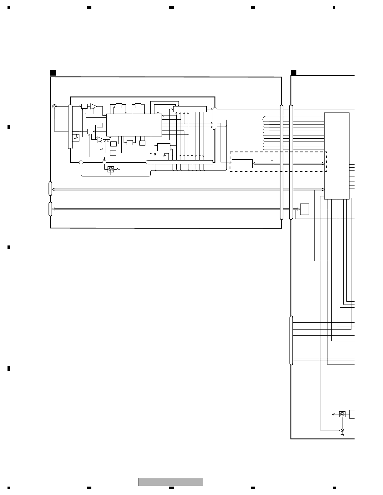
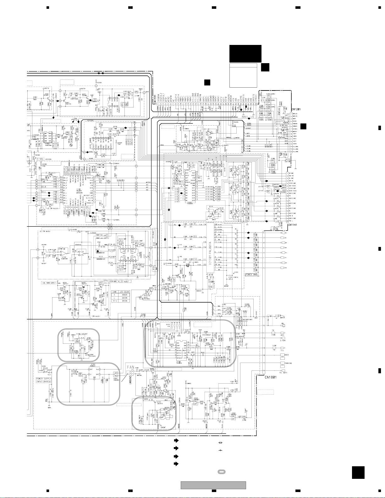
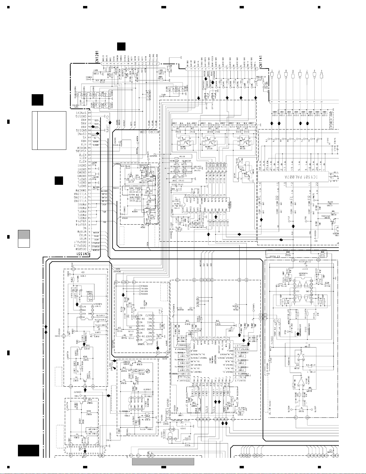
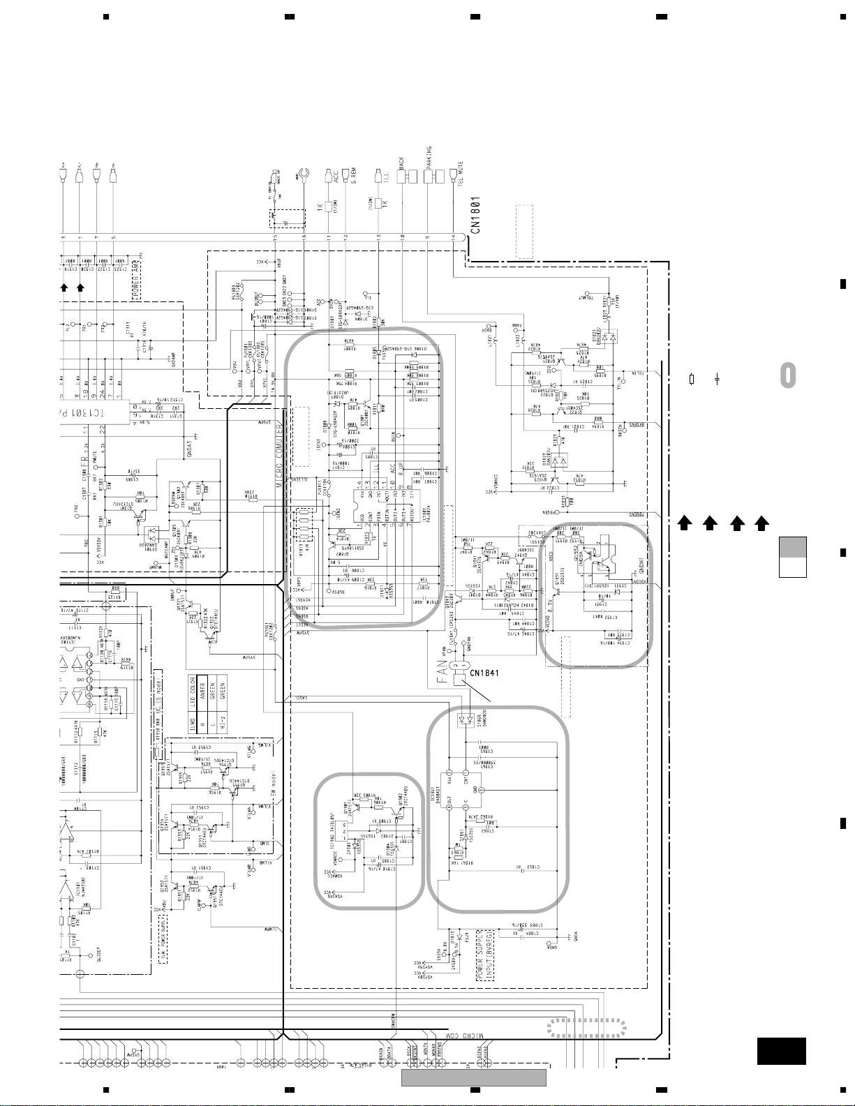
3. BLOCK DIAGRAM AND SCHEMATIC DIAGRAM
3.1 BLOCK DIAGRAM(1)
A
(2/2)MOTHER PCB
A
(UC,EW)
NAVI. INPUT
AUX VIDEO
VTR1LCH INPUT
VTR1RCH INPUT
B
FL,RL,PRE_L
REAR VIDEO
GRILLE PCB
C
RESET
7 7
KDT0-2
VILLONA,
VILLONG,
VILLONB
5
4
CN3831
16
11
CN3802
54
M
Remote control
MD
LD(—)
FO+
TO+
Detach
sensor
sensor
CN101
5
17
4
3
9
7
12
10
1
2
3
4
11
6
J
AC/F/E/BD
CN901
CONTST/SP
KDT0-2
KEY
MATRIX
ILLUMINATION
C
DETACH GRILLE ASSY
PU UNIT(SERVICE) (P8)
MONITOR
DIODE
+5V
HOLOGRAM
UNIT
LASER
DIODE
FOCUS ACT.
TRACKING ACT.
CARRIAGE
MOTOR
SPINDLE
MOTOR
EC
VM
VCC
M
LOADING
MOTOR
M
FG
CLAMPSW
D
CN1226 CN1331 CN4801 CN4802
CCR
1
CCG
2
CCB
3
CCSYNC
4
YS
8
CCREM
18
CN1141
AUXV
6
AUXIAL
4
AUXIAR
2
REAVI
8
CN1201
KEYRES
REMCOM
5
DSENS
4
CD CORE UNIT
RF AMP
8
MDI
IC 201
TA2153FN
Q101
9
LDO
Q102
13
11
15
IC 401
16
BA5811FM
22
VD
V+5
10
9
MUTE
21
SOUND INPUT ISO.
13 1
12 8
14,16,18
HIGH OUT
4
HOME
SW
X601
1
2
V+5
31
IC 1131
TA2050F
IC 1141
(1/2)
PA2028A
58
IC 1801(1/2)
PAJ002A
XI
IC 301
TC9495F2
HOME
CDMUTE
X2
IC 601
PE5273A
X1
CDLOAD
CDEJET
CONT
SPDIFG
DSCSNS
REGULATOR
4
VD
37
CD5VON
+5V
IC 801
BA05SFP
XO
LO
2
66
9
10
4
5
3
73
58
IC1451
NJM2137V
VIDEO AMP
IC1071
NJM2267V
CN701
77
X301
78
LOUT
85
Q302
VDD
Q301
RESET
RESET
7
7
BSRQ52
BRST77
BSCK
1
BRXEN29
BDATA2
31
1
VD
4
IC1971
IC1971
TC7SH08FU
TC7SH08FU
1,2
22
20
15
16
17
18
19
8
8
9
11
40
AUXV
LV2
RV2
VOUT1
2
3
1
IC 1065
NJM2246M
VIDEO/AUDIO
SELECTOR
IC 1031
CXA2089Q
(1/2)
2
LT1
CN1251
LOUT
22
BDATA
19
BSCK
17
BSRQ
15
BRXEN
18
BRST
16
RESET
20
VD
8
VOUT2
7
33
Q1181
X1601
2.582912MHz
BUZZER
VSYS8V
Q1183
Q1184
Q1182
(UC,EW)
35
BKCASEL
30
DSENS
CONTROLLER
PE5290A(UC,ES)
PE5291A(EW)
98
BSO
97
BSCK
2
BSRQ
99
BRXEN
100
BRST
11
RESET
15
16
100
Q1065
VCC
VSA5R6
SYSTEM
IC 1601
(2/2)
RXMON
TXMON
SWACPW
DEG0SW
MTR2
MTR1
MTRPW
DEGPUL2
DEGPUL1
95
96
25
BUP
DEG0SW
21
7
6
20
DEGPUL2
4
DEGPUL1
3
ANR
ANG
ANB
CSYNC
SYNCVI
HRX
HTX
VSA5R6
MOREM
YS
PWRFL PWRFL
MTR2
MTR1
MTRPW
RELAY PCB
D
Q922
BUP14V
CSYNC
SYNCVI
SWAC5R6
MOREM
SWACPW
MFLPW
PWRFL
CN4803
DEG0SW
MTR2
MTR1
BUP14
MTRPW
DEGPUL2
DEGPUL1
ANR
29
ANG
30
ANB
31
27
33
HRX
23
HTX
24
21
22
9
YS
25
13
1
1
2
2
32
3
6
10
9
2
1
11
7
8
ANR
36
5
18
18
ANG
37
4
19
19
ANB
38
3
17
17
CSYNC
34
7
20
20
SYNCVI
40
1
15
15
7
7
HRX
10
31
HTX
9
32
SWAC5R6
12
29
MOREM
11
30
SWACPW
23
18
YS
8
33
Q921
15
10
31
14
11
30
13
12
29
DEG0SW
1
40
MTR2
5
36
MTR1
4
37
MTRPW
6
35
DEGPUL2
2
39
DEGPUL1
3
38
18
AVH-P6400CD/UC
1234
Page 19
A
B
5678
CB
CN4802
ANR
ANG
ANB
CSYNC
SYNCVI
HRX
HTX
SWAC5R6
MOREM
SWACPW
YS
MFLPW
PWRFL
DEG0SW
MTR2
MTR1
BUP14 BUP14
V
MTRPW
DEGPUL2
DEGPUL1
F
CN2
29
29
30
30
31
31
27
27
33
33
23
23
TXD
24
24
SWAC56
21
21
REM
22
22
9
9
25
25
13 13
22
1
1
1
2
2
2
32
3
3
VILLMB,VILLMG,VILLMA
H
CN2804CN4803
DEG0SW
6
6
MTR2
2
10
MTR1
3
9
11
2
10
1
MTRPW
1
11
DEGPUL2
5
7
DEGPUL1
4
8
MONITOR PCB
ANR
ANG
ANB
CSYNC
CVBS
RXD
YS
MFLPW
PWRFL
ENCODER PCB
Q2803
Q2801
Q2804
FILTER
Q131
Q121
Q111
SYMC AMP
Q141
2,3 2
IC 142
TK15404MI
Q101
5->3V CHANGE
35
KEY0-2
Q603
RESET
12
IC 602
S-80835ANNP-EDZ
VACC5V
X601
10MHz
VILLMB,VILLMG,VILLMA
23
IC 2801
1
TA7806S
IC 2802
TA78L05F
4
7
5
3
IC 2804
TC7S14FU
IC 2807
TC7W14FU
1
Q2802
Q133
Q132
Q123
Q122
Q113
Q112
5->3 CHANGE
62
IC2(1/2)
TC7WH34FU
Q103
Q102
IC2(2/2)
TC7WH34FU
35
TSO
36
TSI
81
MFLPW
7
10
12
13
15
REMIN
VDDSENS
SYSTEM
CONTROLLER
RESET
IC 601
PD5747A
XOUT
XIN
DIMDTY
TC7S08FU
6
BA6951FS
5
10
VCC
2
1
3
24
2
IC 603
4
IC 2803
OSDCLK
LSEN
MVIPW
INVPUL
3
2
3
2
52
53
54
18
65
93
17
2
82
26
9
7
IC 2806
GP1S25
IC 2805
GP1S25
RIN
GIN
BIN
HDIN
CVI1
FNAVI
TWO PICTURES
CONTROL IC
IC 1
TC90A64AF
POLC
28
6
IC 92
TC7S08FU
IC 651
S-29131AFJ
EEP-ROM
8.0V
PWRFL
CN2805
MOP
MOM
CN2806
DEG0SEN1
RGB AMP
734
1
NJM2138V
1438
5.0V
1
3
3.3V
1
2.5V
15
8V
7
18V
8
-12V
Q832
14.4V
3.3V
3.3V
KEY3,4
Q153
Q152
Q151
Q182
Q183
7
IC 82
TC7WH34FU
IC 851
2
LT1376CS8
IC 841
2
R1130H251B
IC 861
4
MAX1748EUE
POWER SUPPLY
ROUT
36 4
GOUT
BOUT
82
X0
X1
42MHz
X1
83
101
SCKE
VCOM AMP
IC 181
NJM082BV
24
VCC
Q835
DIMDTY
1
Q831
5V
12
9
10
11
4
CN3
INVERTER PCB
E
1
MOTOR
2
SW PCB
I
S2801
1
2
CN941
1
2
3
8
PWRFL
DIMDTY
KEY
MATRIX
FU941
315,14,15
IC 942
TA78L05F
Q941
IC 151
Q156
Q155
Q154
Q942
1
TC7SH08FU
CN801
CN5 CN811
VACC 5
IC 945
4
18
7
8.0V
VR
28
VG
27
VB
26
VCOM
17
234
LSEN
7
INVERTER FOR
BACK LIGHT
IC 941
OZ961IS
10
LCD MODULE
LCD
LCD
BACK LIGHT
UPPER PCB
G
OUT OF LIGHT SENSOR
IC 811
NJM062V
Q943
20
Q944
11
37
CN942
T941
C
1
2
FL1
FL2
D
AVH-P6400CD/UC
56
7
8
19
Page 20
1234
N
A
W
T
C
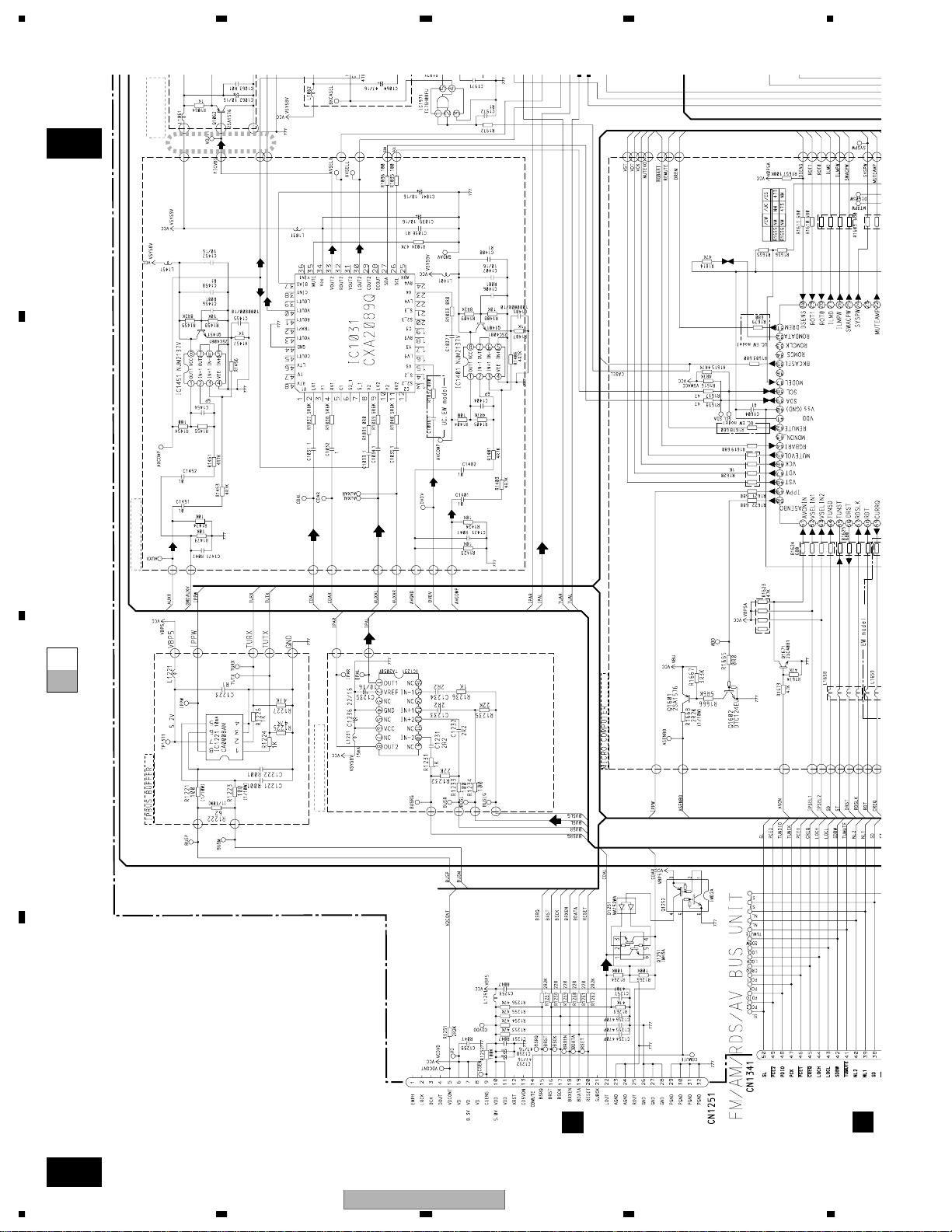
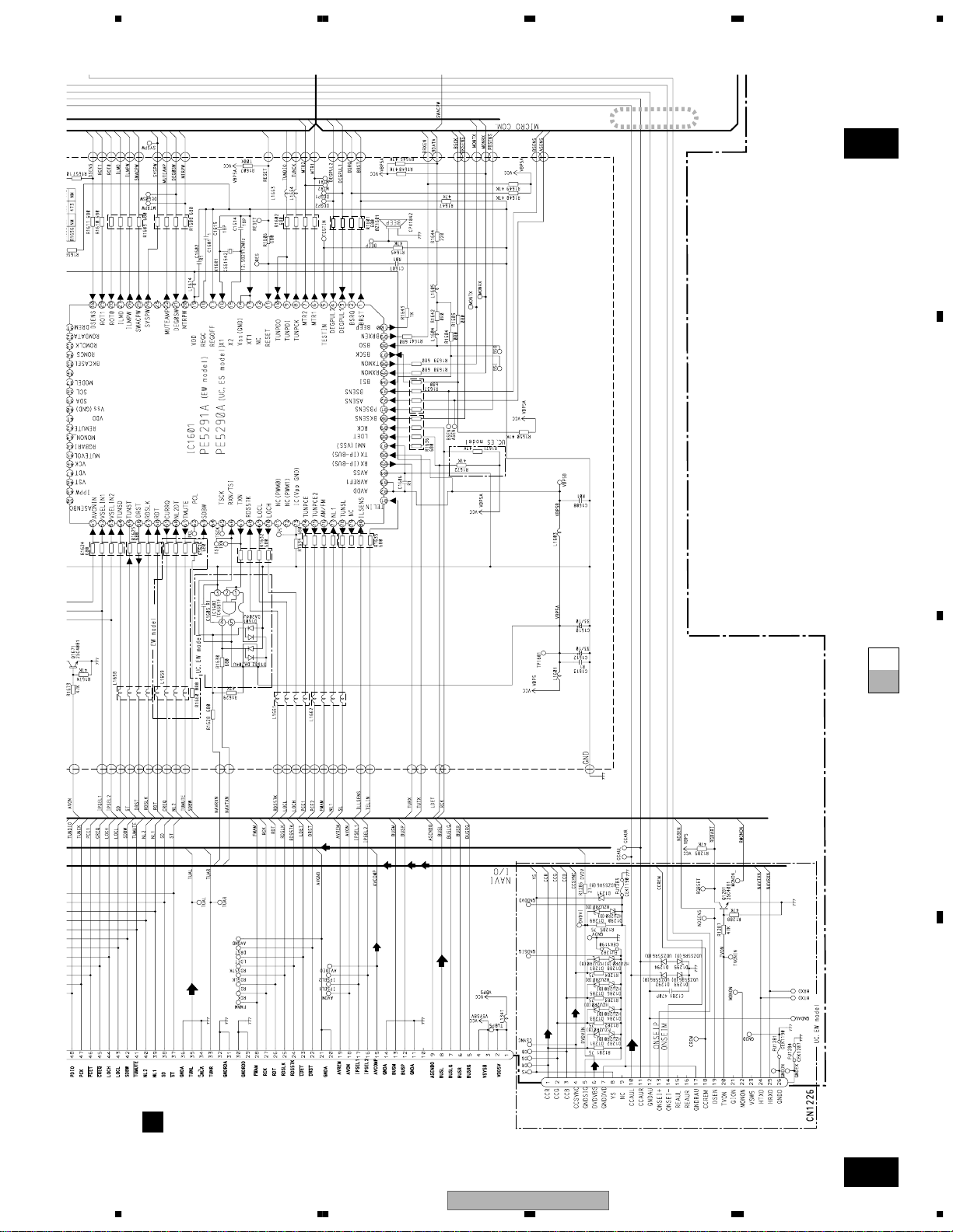
3.2 BLOCK DIAGRAM(2)
A
AV BUS CONNECTOR
B
MAIN ANT
CN2403
IP BUS INPUT
CN2404
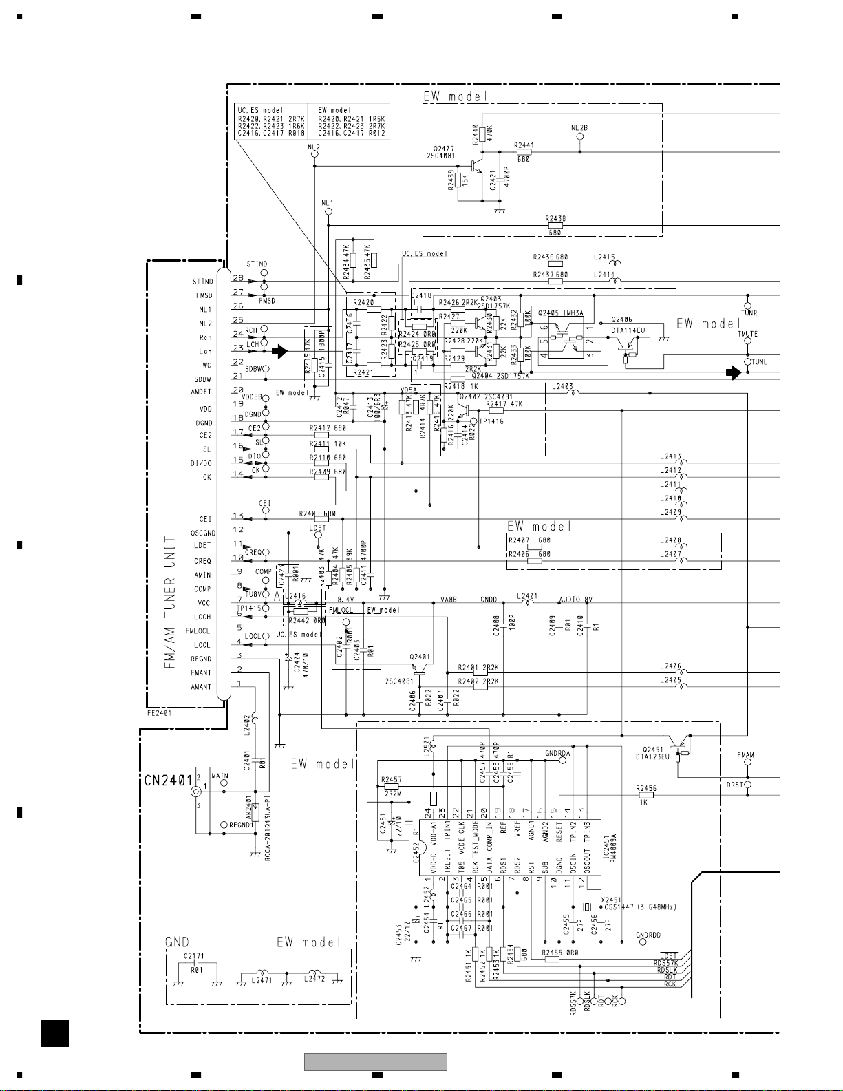
TUNER PCB
B
FM/AM TUNER UNIT
CN2401
1
2
3
12
AVCOMP,AVON,IPSEL1,2
BUSP,BUSM,BUSL,BUSR,BUSRG,BUSLG
AMANT
FMANT
RFGND
AMPS
MOTHER PCB(2/2)
A
FM/AM 1ST IF 10.7MHz
AMRF
ATT
T51 Q51 CF51
ANT ADJ
ATT
FMRF
IMG ADJ
RF ADJ
LOCH
6
LOCL
4
Q2401
CF52 CF53
IC1
MIXER, IF AMP, DET.
CF202
AM 2ND IF
450kHz
VSYS8V
MPXREF 41kHz
AMDET
X901
10.25MHz
EEPROM
CREQcreq
DI/DO
10
15 17 14 13 21 16 27 26 25
PDIO
IC 3
CN2402
NL1(EW)
NL2(EW)
RDS57K,RDSLK,
RDT,RCK,DRST,FMAM
TUNL
PDIO
pce!
LOCL
LOCH
creq
ldet
pce@
PCK
COMP
LDET
L ch
23
8
11
IC 2 FM MPX
(EW)
NC
DGND
CE2
CKPCK
CE1
SDBWSLFMSD
18
pce!
pce@
STIND
NL1
NL2
28
SL
SD
NL1
NL2
st
20
RDS
IC 2451
PM4009A
CN1341
TUNL
16
35
28
23
2
49
SL
1
50
3
48
4
47
st
14
37
SD
13
38
46
5
43
8
44
7
45
6
39
12
40
11
AVCOMP,AVON,IPSEL1,2
TA2050F
BUSP
NL2DT(EW)
RDS57K,RDSLK,
RDT,RCK,DRST,FMAM
IC1231
IPAL
1
AVCOM
LDET
TUNPCE2
TUNSL
TUNPDIO
TUNPCK
TUNST
TUNSD
TUNPCE
LOCH
CURRQ
NL1(EW)
LOCL
88
75
78
9,10
8
55
54
74
69
70
59
77
60
SYSTEM
CONTROLLER
IC 1601
PE5290A(UC,ES)
PE5291A(EW)
25
SWACPW
91
81
TELIN
pbsens
(1/2)
90
BKSENS
80
ILSENS
93
BSENS11RESET
IPP
49
RX
85
TX
86
BK
35
TXN
67
ASE
92
RX
66
44
RGB
C
CN1226
CCAUL
10
TVON
20
HTXD
NAVI
24
I/O
HRXD
25
ONSEI +
13
ONSEI-
14
Q1901
VBU
D
SWACPW
3
Q1902
20
AVH-P6400CD/UC
1234
Page 21

A
B
4
S
5678
CN1801
12
5
7
1
3
6
8
2
4
15
+
16
S.ANT
+
RL
RL
+
RR
RR
+
FL
FL
+
FR
FR
BACK UP
GND
11
13
10
14
9
TEL MUTE
ACC
C
ILL
BACK
PAR KIN G
MOTHER PCB(2/2)
A
IC 1141
(2/2)
PA2028A
Q1822
R.REM
RL
RL
RR
RR
FL
FL
FR
FR
4
25
21
+
23
17
+
19
5
+
3
9
+
7
IC1861
BA00AST
BUP
FU1801
VPFL
FU1802
VPVI
FU1803
VBU
ACC
Q1821
2
1
BUP
GUIDE MIX
6
IC1101
Q1303
VBUP5V
IC 1801
(2/2)
PAJ002A
CONT
FL
1
Q1321
Q1802
2
Q1801
9
IN3
10
IN2
12
IN1
CN2402
TUNL
ldet
pce@
PDIO
PCK
pce!
LOCL
LOCH
creq
NL1(EW)
NL2(EW)
RDS57K,RDSLK,
RDT,RCK,DRST,FMAM
51
09A
CN1341
TUNL
16
35
28
23
2
49
SL
1
50
3
48
4
47
st
14
37
SD
13
38
46
5
43
8
44
7
45
6
39
12
40
11
AVCOMP,AVON,IPSEL1,2
IC1231
TA2050F
BUSP
TUNPCE2
TUNSL
TUNPDIO
TUNPCK
TUNST
TUNSD
TUNPCE
CURRQ
NL1(EW)
NL2DT(EW)
RDS57K,RDSLK,
RDT,RCK,DRST,FMAM
IPAL
1
AVCOM
LDET
88
75
78
9,10
8
55
54
74
LOCL
69
LOCH
70
59
77
60
PE5290A(UC,ES)
PE5291A(EW)
25
SWACPW
91
SYSTEM
CONTROLLER
IC 1601
(1/2)
81
90
80
TELIN
ILSENS
pbsens
BKSENS
93
BSENS11RESET
GUIDE SOUND INPUT
+
IC1221
6
ASENS
3
2
Q1302
5
7
6
11
NJM4558E
OUT2
RSTOUT
OUT3
OUT1
ONSEI
IPPW
49
RX
85
TX
86
BKCASEL
35
TXN
67
ASENS
92
RXN
66
44
RGBARI
8
2
1
IC1602
TC4S81F
1,2
4
ONSEI
CA0008AM
CN1226
CCAUL
10
TVON
20
HTXD
NAVI
24
I/O
HRXD
25
ONSEI +
13
ONSEI-
14
IC 1102
NJM2058V
Q1301
BUP
Q1322
ACC
1
12
FLIN
4
SYSPW
POWER AMP
IC1301
PAL007A
22
MUTE
RLIN
14
10
11
9
7
12
11
41
42
43
IC 1001
PML009A
40
30
IC 1031
(2/2)
CXA2089Q
1
IC1401
NJM2137V
3
BUP
VSWACC
VSYS8V
VSYS9V
Q1823
VBU
SWACPW
Q1901
Q1902
3
IC 1902
TA78L05F
1
VSWACC
BUP
AVH-P6400CD/UC
56
Q1841
7
Q1842
Q1843
FU1841
CN1841
FAN
2
1
D
21
8
Page 22
1234
3.3 OVERALL CONNECTION DIAGRAM
A
VTR Sound input(R)
VTR Sound input(L)
VTR input
Rear Video output
Pre out
TENNA
AN
/FM
AM
Sub W
ofer
output
T PIN
TPU
AV OU
B
A
B
C
C
M
ACC
CO
VSW
DSENS
REM
VI I/O
A
N
S
M
ACC
CO
D
22
1234
DSEN
VSW
REM
AVH-P6400CD/UC
Page 23
A
B
5678
CN701
RELAY
H
D
F
E
I
C
G
J
AVH-P6400CD/UC
56
D
7
23
8
Page 24
1234
3.4 MOTHER PCB(GUIDE PAGE)
Note: When ordering service parts, be sure to refer to " EXPLODED VIEWS AND PARTS LIST" or
"ELECTRICAL PARTS LIST".
Large size
A-b
A-b
SCH diagram
Guide page
Detailed page
N
IO
T
A
L
O
IS
T
U
P
IN
D
N
U
O
S
IP
A
A-a A-b
A-a
A-a
A-a
M
I
ER
T
PU
M
O
C
O
R
IC
M
T
C
E
L
E
S
D
N
U
O
S
E
G
A
V
5R1K
5R1K
V
V
V
V
V
V
T
U
P
T
U
O
R
O
T
I
N
O
M
R
E
F
F
U
B
T
T
A
V
1
0K
82
R
B
V
V
T
C
L
E
S
A
R
E
M
A
C
K
C
A
B
B
J
CN701
CD
: 3.28dBs
13.7V
s
B
d
.5
9
1
: -
)
S
,E
C
U
(
M
F
C
U
(
M
A
M
F
M
A
R
E
IV
R
D
d
n
a
R
O
IT
N
O
M
S
IP-BU
s
B
d
.0
0
3
: -
)
S
,E
CD
s
B
d
.5
5
) : 1
W
E
(
VTR
s
B
d
.0
6
2
: -
)
W
E
(
VI
A
N
IS
T
U
P
IN
D
N
U
O
S
E
ID
U
G
B
CN2402
FM(UC,ES) : -19.50dBs
AM(UC,ES) : -30.00dBs
FM(EW) : -15.50,dBs
AM(EW) : -26.00dBs
C
V
V
S : 2.2dBs
IP-BU
R
S
V
2
>
V
R
S
s
VI : 2.2dB
A
A
A
2
>
N
2
D
A
2
>
A
5
.1
3
>
A
24
AVH-P6400CD/UC
1234
Page 25
A
B
5678
A-b
Mother Tuner Unit
R
S
R
O
IT
N
O
M
R
A
E
T
U
P
T
U
(
M
F
U
(
M
A
M
F
M
A
R
R
E
F
F
U
B
V
FM
A
O
S
IS
4.3V
4.3V
(U
(U
M
FM
M
A
4.3V
4.3V
IN
D
N
U
N
O
I
T
A
L
O
,ES) : -1.6dB
C
C,ES) : -6.9dB
) : 4.6dBs
(EW
) : -2.9dBs
(EW
68
R
E
F
F
U
. B
O
M
E
R
.
L
O
V
H
G
I
H
,
IN
P
A
C
S : 7.3dBs
: 7.33dBs
R
15.5V
T
U
P
U
IP-B
s
CD
s
TR : 7.33dBs
V
VI : 7.30dBs
A
N
V
V
T
C
L
E
S
A
R
E
M
A
C
K
C
A
B
s
B
d
.5
9
1
: -
)
S
E
,
C
.0
0
3
: -
)
S
,E
C
.5
5
: 1
)
W
E
(
.0
6
2
: -
)
W
E
(
O
S
E
ID
U
G
U
d
d
d
N
s
B
s
B
s
B
IN
D
IP-BU
CD
VTR : 2.23dBs
A
N
T
U
P
: 2.20dB
S
: 3.23dBs
VI : 2.20dB
. M
O
IS
s
s
.
IX
V
V
4.3V
D
CN4801
N
O
M
R
O
IT
Consists of
Mother PCB
Tuner PCB
Grille PCB
Relay PCB
Inverter PCB
R
E
IV
R
D
d
n
a
A
m
0
0
2
>
S
V
8
6
CD : 33.33dBs
A
VTR : 2.20dBs
>
MOTHER PCB
A
2
>
V
V
(
A
5
.2
1
)
C
CN3831
D
N
U
O
S
E
ID
U
G
4.3V
13.8V
>
>
µH
0
7
2
A
.6
1
A
.6
A
.6
1
>
5.0V
5.6V
S
R
E
W
O
P
7.5V
>
A
.3
2
FAN
MOTOR
M1
CXM1193
)
D
V
D
C
(
T
U
P
IN
Y
L
P
P
U
S
R
E
W
O
P
>
)
N
A
F
(
T
U
P
IN
Y
L
P
P
U
A
.6
1
>
S
: Composite Sync.
V
: Composite Video
R
: RGB_R
: Audio_L
TER
PU
COM
ICRO
M
m
0
0
4
,
Y
L
P
P
U
S
R
E
W
O
P
.
N
E
S
Y
L
P
P
U
S
R
E
W
O
P
A
NOTE :
Symbol indicates a resistor.
No differentiation is made between chip resistors and
discrete resistors.
Symbol indicates a capacitor.
No differentiation is made between chip capacitors and
discrete capacitors.
The > mark found on some component parts indicates
the importance of the safety factor of the part.
Therefore, when replacing, be sure to use parts of
identical designation.
AVH-P6400CD/UC
56
1
A
5
.2
1
>
P
P
U
S
R
E
W
O
P
E
,S
N
C
(
T
U
P
IN
: The power supply is shown with the marked box.
7
>
Y
L
)
E
S
N
Decimal points for resistor
and capacitor fixed values
are expressed as :
←
2.2 2R2
←
0.022 R022
C
D
A
25
8
Page 26
A
CN2402
A-b
1234
T
U
TP
U
O
R
FFER
O
U
IT
N
O
TT B
A
M
V
1
8
2
0K
R
IV
E
R
M
O
N
IT
O
R
an
d
D
V
V
V
1K
5R
5R
1
K
V
B
V
T
A-b
A-a
A-a
ELEC
S
D
N
U
O
E S
G
A
IM
V
M
ICRO COM
PUTER
V
C
D
A-a
26
N
IO
T
LA
O
T IS
PU
IN
D
N
U
O
IP S
13.7V
s
: 3.28dB
D
C
J
CN701
B
AVH-P6400CD/UC
1234
Page 27
A
B
5678
2
A-b
s
s
s
) : -30.00dB
) : -19.50dB
,ES
,ES
C
C
(U
(U
) : -15.50,dB
M
FM
A
(EW
FM
s
) : -26.00dB
(EW
M
A
A-b
A-a
A-a
VI : 2.2dBs
A
N
V
S
V
R
V
: 2.2dBs
S
IP-BU
S
R
V
2A
>
2A
>
2A
>
3.15A
>
C
D
B
CN2402
AVH-P6400CD/UC
56
A-a
7
27
8
Page 28
1234
C
CN3831
A
2A
MOTHER PCB
>
V
: 2.20dBs
TR
V
V
( )
1.25A
>
A
: 33.33dBs
D
R
Mother Tuner Unit
Consists of
Mother PCB
Tuner PCB
Grille PCB
Relay PCB
Inverter PCB
B
D
CN4801
V
S
6
8
>
20
0
m
E
IV
R
D
and
R
ITO
N
O
M
A
C
C
D
A-b
A-a
A-b
28
15.5V
L.
O
V
FFER
U
. B
O
EM
R
68
V
R
S
V
V
R
O
IT
N
O
M
R
FFER
U
EA
B
R
T
TPU
U
R O
FFER
U
ITO
N
O
TT B
A
M
V
V
ELCT
S
V
ERA
M
A
C
K
C
A
B
1
H
IG
,H
PIN
CA
R
CD : 7.33dBs
VTR : 7.33dBs
NAVI : 7.30dBs
IP-BUS : 7.3dBs
T
PU
N
IN
D
TIO
N
LA
U
O
O
IS
S
4.3V
4.3V
8
20
K
FM(EW) : 4.6dBs
4.3V
4.3V
AM(EW) : -2.9dBs
FM(UC,ES) : -1.6dBs
AM(UC,ES) : -6.9dBs
4.3V
CD : 3.23dBs
VTR : 2.23dBs
NAVI : 2.20dBs
IP-BUS : 2.20dBs
s
s
) : 15.5dBs
) : -26.0dB
) : -30.0dB
,ES
,ES) : -19.5dBs
(EW
(EW
C
C
M
FM
(U
(U
A
M
FM
A
G
U
ID
E
S
O
U
N
D
4.3V
.
IX
. M
O
T IS
PU
IN
D
N
U
O
E S
ID
U
G
M
O
N
IT
O
R
an
d
D
R
IV
E
R
AVH-P6400CD/UC
1234
Page 29
A
B
5678
D
←
←
Decimal points for resistor
and capacitor fixed values
are expressed as :
2.2 2R2
0.022 R022
>
E)
S
EN
PPLY
,S
N
SU
R
T(C
E
W
PU
IN
PO
>
1.6A
270µH
1.6A
>
1.25A
>
Symbol indicates a resistor.
: The power supply is shown with the marked box.
No differentiation is made between chip resistors and
discrete resistors.
Symbol indicates a capacitor.
No differentiation is made between chip capacitors and
discrete capacitors.
The > mark found on some component parts indicates
the importance of the safety factor of the part.
Therefore, when replacing, be sure to use parts of
: RGB_R
identical designation.
: Audio_L
A-b
A-a
NOTE :
.
EN
S
,
PPLY
PPLY
U
U
S
S
ER
ER
W
W
PO
PO
A
400m
>
)
N
T(FA
U
P
IN
PPLY
SU
ER
W
PO
>
1
.6A
: Composite Sync.
: Composite Video
S
V
R
7.5V
1.6A
>
G
U
ID
E
S
O
U
N
4.3V
13.8V
5.0V
5.6V
2.3A
>
M1
MOTOR
FAN
)
D
V
D
T(C
PU
PPLY IN
SU
ER
W
CXM1193
PO
C
D
AVH-P6400CD/UC
56
2
A-b
7
29
8
Page 30
1234
3.5 TUNER PCB
A
B
C
RDS decoder
0R0)
L2453
(R2460
D
B
30
1234
AVH-P6400CD/UC
Page 31

A
B
5678
V
: Composite Video
: Audio_L
Mother Tuner Unit
Consists of
Mother PCB
Tuner PCB
Grille PCB
Relay PCB
Inverter PCB
TUNER PCB
B
V
A
CN1341
2A
2A
>
>
V
C
A
200m
>
D
AVH-P6400CD/UC
56
B
7
31
8
Page 32

1234
3.6 GRILLE PCB
A
A
CN1201
B
C
GRILLE PCB
DETACH GRILLE ASSY
C
Mother Tuner Unit
Consists of
Mother PCB
Tuner PCB
Grille PCB
Relay PCB
Inverter PCB
D
C
32
1234
AVH-P6400CD/UC
Page 33

A
B
5678
3.7 RELAY PCB
D
RELAY PCB
A
CN1331
V
R
S
R
S
S
: Composite Sync.
V
: Composite Video
R
V
: RGB_R
F
CN2
Mother Tuner Unit
Consists of
Mother PCB
Tuner PCB
Grille PCB
Relay PCB
Inverter PCB
S
R
V
C
H
CN2804
D
AVH-P6400CD/UC
56
D
7
33
8
Page 34

1234
3.8 INVERTER PCB
A
F
CN3
1R5K
1R5K
EW
m
odel
1
B
C
>
D
E
34
1234
AVH-P6400CD/UC
Page 35

A
B
5678
o
Mother Tuner Unit
INVERTER PCB
E
Consists of
Mother PCB
Tuner PCB
Grille PCB
Relay PCB
Inverter PCB
del
SELECT
1
2
3
1
2
3
To Back light
2
3
C
AVH-P6400CD/UC
56
560
D
E
7
35
8
Page 36

1234
3.9 MONITOR UNIT
A
For
test mode
V
R
R
V
R
V
B
2-3
6-3
V
E
CN941
CN2
D
CN4802
C
2-1
S
R
V
S
6-2
S
R
V
3-1
6-1
4-1
S
5-2
5-4
5-3
INTERFACE
D
F G
36
2-2
O
G
PEN/CLOSE
UPPER PCB
Monitor Unit
Consists of
Monitor PCB
Upper PCB
AVH-P6400CD/UC
1234
Page 37

A
B
5678
Monitor Unit
Consists of
Monitor PCB
Upper PCB
MONITOR PCB
F
>
R
3-2
4-2
V
R
S
S
5-1
1-1
3-3
1-2
1-3
1-4
3-4
R
8-2
R
7-1
8-1
8-4
7-2
TERFACE
alti Pictues
M
Processing
age
Im
Processing
S
AVH-P6400CD/UC
56
R
S
: Composite Sync.
V
: Composite Video
R
: RGB_R
7
LCD
MODULE
C
8-3
D
F
37
8
Page 38

1234
- Waveforms
A
B
1-1 IC851 3pin 5V
1.00µs
Note: The encircled numbers denote measuring pointes in the circuit diagram.
Ch1 1-2 IC861 15pin 5V
Ch2 1-3 IC861 12pin 5V
Ch3 1-4 IC861 10pin 5V
400µs
Ch1 2-1 DIMDTY 2V
Ch2 2-2 LSEN 2V
1.00µs
Ch1 2-3 INVPUL 2V
frequency : 98.09 kHz
Ch2 2-3 INVPUL 2V
frequency : 104.2 kHz
4.0µs
Ch1 3-1 ANG 500mV
Ch2 3-2 ANG2 500mV
Ch3 3-3 GOUT 500mV
Ch4 3-4 VG 500mV
20.0µs
Ch1 Input 10 STEP VTR IN
Ch2 4-1 CVBS 500mV
Ch3 4-2 CVBS2 500mV
200µs
C
Ch1 Input 10 STEP VTR IN 1V
Ch2 4-2 CVBS 2V
D
Ch3 3-3 GOUT 1V
Ch4 3-4 VG 5V
Ch1
Ch2
Ch3
Ch4
5-1 V33 2V
5-2 PIPRES 5V
5-3 PIPCK 5V
5-4 PIPDA 5V
10.0µs
Ch1
Ch2
Ch3
Ch4
5-1 V33 2V
5-2 PIPRES 5V
5-3 PIPCK 5V
5-4 PIPDA 5V
20.0µs
38
AVH-P6400CD/UC
1234
Page 39

A
B
5678
Input 10 STEP VTR IN 1V Ch1
6-1 OSDH 5V
Ch2
6-2 OSDV 5V
Ch3
6-3 OSDBLK 5V
Ch4
Input SG10 step VIRIN
Input 10 STEP VTR IN 1V Ch1
8-1 CX 5V
Ch2
8-2 STH1 5V
Ch3
Ch4
3-4 VG 5V
1.0µs
20.0µs
Input 10 STEP VTR IN 1V Ch1
6-1 OSDH 5V
Ch2
6-2 OSDV 5V
Ch3
6-3 OSDBLK 5V
Ch4
Input SG10 step VIRIN
Input 10 STEP VTR IN 1V Ch1
8-1 CX 5V
Ch2
8-2 STH1 5V
Ch3
Ch4
3-4 VG 5V
20.0µs
400µs
Ch2
Ch3
Ch4
Input 10 STEP VTR IN 1V Ch1
7-1 POL 5V
7-2 VCOM 5V
3-4 VG 5V
20.0µs
Input 10 STEP VTR IN 1V Ch1
8-4 CPH 2V
Ch2
3-4 VG 5V
Ch3
400µs
Ch2
Ch3
Input 10 STEP VTR IN 1V Ch1
8-4 CPH 2V
3-4 VG 5V
20.0µs
AVH-P6400CD/UC
56
C
D
39
7
8
Page 40

1234
3.10 ENCODER UNIT
A
M1
CXB7612
Drive Motor
M
White
Red
DEG0
ENCODER PCB
H
Black
Yellow
Encoder Unit
Consists of
Encoder PCB
SW PCB
B
SW PCB
I
C
D
H I
40
D
CN4803
AVH-P6400CD/UC
1234
Page 41

A
B
5678
C
AVH-P6400CD/UC
56
D
41
7
8
Page 42

1234
3.11 CD MECHANISM MODULE
CD CORE UNIT
J
A
PICKUP UNIT(SERVICE)(P8)
F
SL
SL
220K
RF AMP
SL
SL
SL
F
330K
B
SL
SIGNAL LINE
F
FOCUS SERVO LINE
T
TRACKING SERVO LINE
C
CARRIAGE SERVO LINE
S
SPINDLE SERVO LINE
C
SWITCHES:
CD CORE UNIT
S901 : LOAD,EJ SWITCH………ON-OFF
S902, 903 : LOAD,EJ SWITCH………ON-OFF
S904 : HOME SWITCH …………ON-OFF
The underlined indicates the switch position.
LOADING MOTOR
M2 CXB6340
T
T
F
SL SL
F
T
F
T
CARRIAGE MOTOR
M1 CXB6361
C
C
RED
BLACK
WHITE
F
SL
T
T
F
F
T
F
T
!
F
SL
T
T
5
T
SL
4
F
8200P
SL
F
T
F
T
6
T
C
C
F
T
C
2
7
1
#
T
T
F
5V
REGULATOR
F
F
T
ACT / MOTOR DRIVE
3
F
T
S
C
C
)
S
S
9
C
C
S
C
S
S
D
SPINDLE MOTOR
M3 CXB6620
S
S
0
J
42
1234
AVH-P6400CD/UC
Page 43

A
B
5678
33P
220K
330K
Q301
CDMUTE
SL
F
T
F
T
SERVO CONTROL / DSP / DAC / LPF
C321
SL
4R7/35
C322
4R7/35
R307
1K
R306
1K
R317
R318
22K
22K
6
5
4
D301
MA151WA
SL
SL
IMD2A
5
4
3
Q302
FMG12
1
2
3
1
2
&
LOUT
*
ROUT
S
C
(
@
8
R319
330
CSS1525
16.934MHz
X301
S
C
SL
)
VDCONT
⁄
R713
CSENS
PE5273A
CD MECH. CONTROLLER
S
R605
R606
22K
47K
BSRQ
BSCK
BRXEN
BDATA
SUBOK
R702
R711
R701
220
220
0R0
CDMUTE
SL
R709
0R0
CSENS
XRST
CD5VON
CDMUTE
BSRQ
BRST
BSCK
BRXEN
BDATA
RESET
SUBOK
SL
C
D
A
CN1251
AVH-P6400CD/UC
56
J
7
43
8
Page 44

1234
- Waveforms
Note:1. The encircled numbers denote measuring pointes in the circuit diagram.
2. Reference voltage
VREF:2.1V
1 CH1:DSCSNS 5V/div.
A
2 CH2:CDLOAD 5V/div.
3 CH3:CDEJET 5V/div.
⁄ CH4:VD 5V/div.
8cm LOAD
→
GND
→
GND
→
GND
→
GND
1 CH1:DSCSNS 5V/div.
2 CH2:CDLOAD 5V/div.
3 CH3:CDEJET 5V/div.
B
12cm EJECT
→
GND
→
GND
→
GND
500ms/div.
500ms/div.
1 CH1:DSCSNS 5V/div.
2 CH2:CDLOAD 5V/div.
3 CH3:CDEJET 5V/div.
⁄ CH4:VD 5V/div.
12cm LOAD
→
GND
→
GND
→
GND
→
GND
4 CH1:RFO 500mV/div.
5 CH2:TEY 500mV/div.
Tracking open
→
VREF
→
VREF
500ms/div.
2ms/div.
1 CH1:DSCSNS 5V/div.
2 CH2:CDLOAD 5V/div.
3 CH3:CDEJET 5V/div.
8cm EJECT
→
GND
→
GND
→
GND
5 CH1:TEY 500mV/div.
6 CH2:FEY 500mV/div.
Setup
→
VREF
→
VREF
500ms/div.
200ms/div.
7 CH1:FD 1V/div.
8 CH2:fok 5V/div.
9 CH3:SINY 5V/div.
Setup
C
→
VREF
→
VREF
→
VREF
6 CH1:FEY 500mV/div.
@ CH2:foon 5V/div.
Setup(Focus close)
→
VREF
D
→
VREF
500ms/div.
1ms/div.
7 CH1:FD 2V/div.
8 CH2:fok 5V/div.
0 CH3:FG 5V/div.
9 CH4:SINY 5V/div.
Setup(In focus)
→
VREF
→
VREF
→
VREF
→
VREF
6 CH1:FEY 200mV/div.
7 CH2:FD 500mV/div.
Setup(Focus AGC)
→
VREF
→
VREF
100ms/div.
1ms/div
7 CH1:FD 1V/div.
! CH2:FOP 2V/div.
Setup(In focus)
→
VREF
→
VREF
5 CH1:TEY 200mV/div.
.
# CH2:TD 200mV/div.
Setup(Tracking AGC)
→
VREF
→
VREF
200ms/div.
1ms/div.
44
AVH-P6400CD/UC
1234
Page 45

A
B
5678
6 CH1:FEY 500mV/div.
7 CH2:FD 500mV/div.
4 CH3:RFO 1V/div.
Setup(FE Bias adjustment)
→
VREF
→
VREF
→
VREF
9 CH1:SINY 100mV/div.
Play
→
VREF
4 CH1:RFO 2V/div.
( CH2:dfct 5V/div.
7 CH3:FD 1V/div.
# CH4:TD 2V/div.
Play(The defect part passes)
10ms/div.
200ms/div.
500µs/div.
4 CH1:RFO 0.5V/div.
Play
→
VREF
6 CH1:FEY 500mV/div.
7 CH2:FD 500mV/div.
5 CH3:TEY 500mV/div.
# CH4:TD 500mV/div.
Play
→
VREF
→
VREF
→
VREF
→
VREF
4 CH1:RFO 1V/div.
5 CH2:TEY 500mV/div.
( CH3:dfct 5V/div.
CRG move
0.5µs/div.
1ms/div.
50µs/div.
& CH1:LOUT 2V/div.
* CH2:ROUT 2V/div.
Play
→
VREF
→
VREF
5 CH1:TEY 500mV/div.
) CH2:CIN 500mV/div.
Search
200µs/div.
200ms/div.
→
VREF
→
VREF
→
VREF
→
VREF
4 CH1:RFO 1V/div.
5 CH2:TEY 1V/div.
# CH3:TD 1V/div.
Test mode 100TRjump
→
VREF
→
VREF
→
VREF
5ms/div.
→
VREF
→
VREF
→
VREF
4 CH1:RFO 1V/div.
5 CH2:TEY 500mV/div.
# CH3:TD 1V/div.
Test mode 1TRjump
→
VREF
→
VREF
→
VREF
500µs/div.
→
VREF
→
VREF
4 CH1:RFO 1V/div.
5 CH2:TEY 1V/div.
# CH3:TD 1V/div.
Test mode 32TRjump
→
VREF
→
VREF
→
VREF
C
5ms/div.
D
AVH-P6400CD/UC
56
7
8
45
Page 46

1234
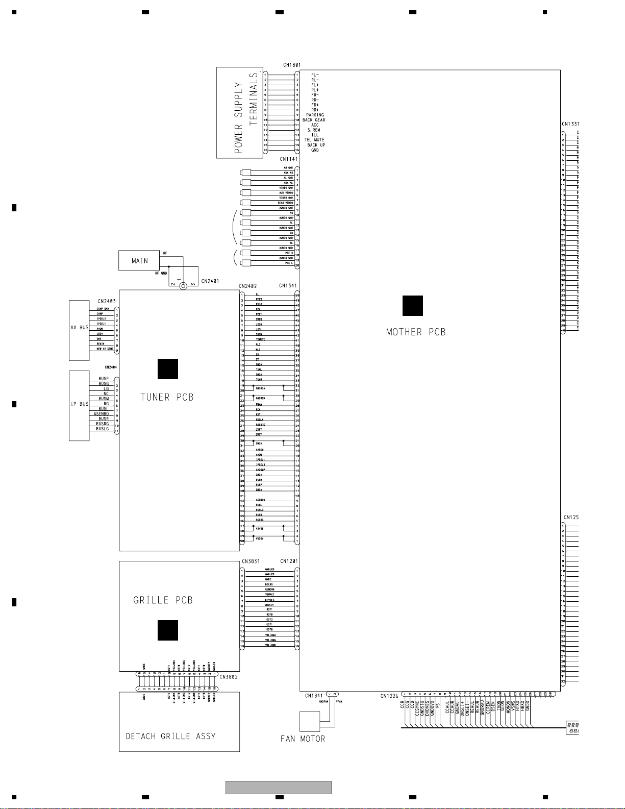
4. PCB CONNECTION DIAGRAM
4.1 MOTHER PCB
A
B
NOTE FOR PCB DIAGRAMS
1.The parts mounted on this PCB
include all necessary parts for
several destination.
For further information for
respective destinations, be sure
to check with the schematic dia gram.
2.Viewpoint of PCB diagrams
Connector
P.C.Board
Capacitor
Chip Part
SIDE A
SIDE B
MOTHER PCB
A
D
CN4801
1
1
C
D
A
46
1234
AVH-P6400CD/UC
Page 47

A
B
5678
SIDE A
1
C
FRONT
AVH-P6400CD/UC
56
D
CN3831
C
A
7
47
8
Page 48

1234
A
B
MOTHER PCB
A
AV OUTPUT PIN
CN2402
B
NAVI I/O
C
SYNCVI
D
A
48
1234
AVH-P6400CD/UC
Page 49

A
B
5678
SIDE B
CN1801
FAN MOTOR M1
POWER SUPPLY TERMINALS
AVH-P6400CD/UC
56
C
CN701
J
D
A
7
49
8
Page 50

1234
4.2 TUNER PCB
TUNER PCB
B
A
B
SIDE A
IP-BUS
AV BUS
TUNER PCB
B
SIDE B
A
CN1341
C
D
B
50
AM/FM
ANTENNA
AVH-P6400CD/UC
1234
Page 51

A
B
5678
4.3 GRILLE PCB
GRILLE PCB
C
RESET
SIDE A
DETACH GRILLE
ASSY
GRILLE PCB
C
SIDE B
CN1201
AVH-P6400CD/UC
56
A
7
C
D
C
51
8
Page 52

1234
4.4 INVERTER PCB
INVERTER PCB
E
A
SIDE A
MENU/SELECT
INVERTER PCB
E
SIDE B
WIDE
MODE
RGB
B
DISP
F
CN3
PWRFL
DIMDTY
C
D
BACK LIGHT
E
52
1234
AVH-P6400CD/UC
Page 53

A
B
5678
4.5 RELAY PCB,UPPER PCB
RELAY PCB
D
H
CN2804
A
F
CN1331
CN2
SIDE A
RELAY PCB
D
SIDE B
UPPER PCB
G
UPPER PCB
G
OPEN/CLOSE
SIDE A
F
SIDE B
C
CN5
D
AVH-P6400CD/UC
56
GD
7
53
8
Page 54

1234
4.6 MONITOR PCB
MONITOR PCB
F
A
LCD
MODULE
B
SIDE A
E
CN941
C
GND
EPRTEST
D
G
CN811
F
54
CN4802
D
AVH-P6400CD/UC
1234
Page 55

A
B
5678
MONITOR PCB
F
VG
VR
VB
SIDE B
VCOM
V8
VM12
V18
CUBS
V5
V33
AND
ANG
VVI
ANR
C
D
AVH-P6400CD/UC
56
F
7
55
8
Page 56

1234
4.7 ENCODER UNIT
ENCODER PCB
H
A
B
SIDE A
M1
I
D
CN4803
ENCODER PCB
H
SIDE B
C
D
H
56
AVH-P6400CD/UC
1234
Page 57

A
B
5678
SW PCB
I
SW PCB
SIDE A
I
SIDE B
DEG0
H
CN2806
C
H
AVH-P6400CD/UC
56
D
I
7
57
8
Page 58

1234
4.8 CD MECHANISM MODULE
CD CORE UNIT
J
A
IC,Q
LOAD, EJ
B
LOAD, EJ
SIDE A
HOME
C
E
D
J
58
AVH-P6400CD/UC
1234
Page 59

A
B
5678
A
CN1251
CD CORE UNIT
J
1
SIDE B
IC,Q
LOAD, EJ
M2 LOADING MOTOR
M3 SPINDLE MOTOR
VREF1
E
F
PICKUP UNIT
(SERVICE)(P8)
AVH-P6400CD/UC
56
C
M1 CARRIAGE MOTOR
D
J
7
59
8
Page 60

1234
5. ELECTRICAL PARTS LIST
NOTE:
• Parts whose parts numbers are omitted are subject to being not supplied.
• The part numbers shown below indicate chip components.
A
Chip Resistor
RS1/_S___J,RS1/__S___J
Chip Capacitor (except for CQS.....)
CKS....., CCS....., CSZS.....
Circuit Symbol and No. Part NamePart No.
Mother T uner Unit
Consists of
Mother PCB
Tuner PCB
Relay PCB
Inverter PCB
Grille PCB
ABCDE
Unit Number:CXX1632(UC model)
Unit Number:CXX1634(ES model)
B
Unit Name:Mother Tuner Unit
MISCELLANEOUS
IC 941 IC OZ961IS
IC 942 IC T A78L05F
IC 945 IC TC7SH08FU
IC 1001 IC PML009A
IC 1031 IC CXA2089Q
IC 1065 IC NJM2246M
IC 1071 IC NJM2267V
IC 1101 IC(UC model) NJM4558E
IC 1102 IC(UC model) NJM2058V
IC 1131 IC TA2050F
IC 1141 IC PA2028A
IC 1221 IC CA0008AM
IC 1231 IC TA2050F
IC 1301 IC PAL007A
C
IC 1401 IC NJM2137V
IC 1451 IC NJM2137V
IC 1601 IC PE5290A
IC 1602 IC(UC model) TC4S81F
IC 1801 IC PAJ002A
IC 1861 IC BA00AST
IC 1902 IC TA78L05F
IC 1971 IC TC7SH08FU
Q 942 Transistor 2SA1774
Q 943 FET SI6544DQ
Q 944 FET SI6544DQ
Q 971 Transistor 2SC4617
Q 972 Transistor 2SC4617
Q 1061 Transistor 2SC4081
Q 1062 Transistor 2SA1576
Q 1064 Transistor 2SA1576
D
Q 1065 Transistor 2SC4081
Q 1071 Transistor 2SA1576
Q 1072 Transistor 2SC4081
Q 1141 Transistor IMD2A
Q 1142 Transistor IMH3A
Q 1143 Transistor IMH3A
Q 1144 Transistor IMH3A
60
1234
Circuit Symbol and No. Part NamePart No.
Q 1181 Transistor 2SC4081
Q 1182 Transistor(UC model) 2SC4081
Q 1183 Transistor DTA114EU
Q 1184 Transistor DTC144EU
Q 1185 Transistor(UC model) DTC144EU
Q 1186 Transistor(UC model) 2SC4081
Q 1251 Transistor IMH3A
Q 1252 Transistor IMD2A
Q 1281 Transistor(UC model) 2SC4081
Q 1301 Transistor DTC124EU
Q 1302 Transistor 2SC4081
Q 1303 Transistor 2SC4081
Q 1321 Transistor 2SA1577
Q 1322 Transistor DTC144EU
Q 1401 Transistor 2SC4081
Q 1451 Transistor 2SC4081
Q 1601 Transistor 2SA1576
Q 1602 Transistor DTC124EU
Q 1671 Transistor 2SC4081
Q 1801 Transistor 2SC4081
Q 1802 Transistor 2SB1184F5
Q 1821 Transistor 2SA1576
Q 1822 Transistor 2SC4081
Q 1823 Transistor 2SA1576
Q 1841 Transistor 2SA1576
Q 1842 Transistor 2SC4081
Q 1843 Transistor 2SD2098
Q 1901 Transistor 2SA1577
Q 1902 Transistor DTC144EU
Q 1931 Transistor 2SD2375
Q 1932 Transistor IMD3A
Q 1951 Transistor DTC144EU
Q 1952 Transistor 2SA1577
Q 2401 Transistor 2SC4081
Q 4801 Transistor 2SA1615-Z
Q 4802 Transistor DTC114EK
D 940 Diode HZU6R2(B3)
D 941 Diode HZU6R2(B3)
D 942 Diode HZU6R2(B3)
D 943 Diode MA143
D 944 Diode MA143
D 945 LED CL190UBX
D 946 LED CL190UBX
D 947 Diode UDZS6R8(B)
D 948 Diode UDZS6R8(B)
D 951 LED CL190PGCD
D 952 LED CL190PGCD
D 953 LED CL190PGCD
D 957 Diode 1SS355
D 971 Diode HZU6R2(B3)
D 972 Diode RB751V40
AVH-P6400CD/UC
Page 61

A
B
5678
Circuit Symbol and No. Part NamePart No.
D 1011 Diode 1SS355
D 1071 Diode Network DA204U
D 1141 Diode UDZS5R6(B)
D 1142 Diode UDZS5R6(B)
D 1143 Diode UDZS5R6(B)
D 1144 Diode UDZS5R6(B)
D 1145 Diode HZU2R0(B)
D 1146 Diode HZU2R0(B)
D 1182 Diode 1SS355
D 1183 Diode(UC model) 1SS355
D 1201 Diode Network DA204U
D 1202 Diode Network DA204U
D 1203 Diode Network DA204U
D 1204 Diode Network DA204U
D 1205 Diode Network DA204U
D 1206 Diode Network DA204U
D 1208 Diode Network DA204U
D 1209 Diode Network DA204U
D 1251 Diode MA152W A
D 1281 Diode HZU2R0(B)
D 1282 Diode(UC model) HZU2R0(B)
D 1283 Diode(UC model) HZU2R0(B)
D 1284 Diode(UC model) HZU2R0(B)
D 1285 Diode(UC model) HZU2R0(B)
D 1286 Diode(UC model) HZU2R0(B)
D 1287 Diode(UC model) HZU2R0(B)
D 1288 Diode(UC model) HZU2R0(B)
D 1289 Diode(UC model) HZU2R0(B)
D 1290 Diode(UC model) HZU2R0(B)
D 1291 Diode(UC model) UDZS5R6(B)
D 1292 Diode(UC model) UDZS5R6(B)
D 1293 Diode(UC model) UDZS5R6(B)
D 1294 Diode(UC model) UDZS5R6(B)
D 1295 Diode(UC model) UDZS5R6(B)
D 1301 Diode DAN202U
D 1303 Diode HZU8R2(B3)
D 1601 Diode Network(UC model) DA204U
D 1602 Diode Network(UC model) DA204U
D 1801 Diode S1G-6904G2P
D 1802 Diode S1G-6904G2P
D 1803 Diode S1G-6904G2P
D 1804 Diode S1G-6904G2P
D 1805 Diode 1SS355
D 1806 Diode S1G-6904G2P
D 1807 Diode UDZS18(B)
D 1808 Diode S1G-6904G2P
D 1811 Diode 1SS355
D 1821 Diode DAN202U
D 1822 Diode UDZS6R8(B)
D 1823 Diode DAN202U
D 1841 Diode 1SS355
D 1842 Diode HZU8R2(B1)
D 1861 Diode 1SS355
D 1865 Diode DAN202U
D 1873 Diode FS1J3
D 1902 Diode 1SS355
D 1903 Diode 1SS355
D 1904 Diode 1SS355
D 1931 Diode HZU9R1(B1)
D 1971 Diode HZU4R7(B3)
D 2471 Diode HZU12(B2)
D 2472 Diode HZU12(B2)
D 2473 Diode HZU12(B2)
56
Circuit Symbol and No. Part NamePart No.
D 2474 Diode HZU12(B2)
D 2475 Diode HZU2R0(B)
D 2476 Diode HZU2R0(B)
D 2481 Diode UDZS5R6(B)
D 2482 Diode UDZS5R6(B)
D 2483 Diode UDZS5R6(B)
D 2484 Diode UDZS5R6(B)
L 1001 Inductor LCT A2R2J2520
L 1031 Inductor LCT A100J2520
L 1061 Inductor LCT A150J2520
L 1062 Inductor LCT A150J2520
L 1071 Inductor LCT A100J2520
L 1101 Inductor(UC model) LCTA2R2J2520
L 1131 Inductor LCT A2R2J2520
L 1141 Inductor LCT A101J2520
L 1171 Inductor CTF1306
L 1172 Inductor CTF1306
L 1173 Inductor CTF1306
L 1174 Inductor CTF1306
L 1175 Inductor CTF1306
L 1176 Inductor CTF1306
L 1221 Inductor LCT A2R2J2520
L 1231 Inductor LCT A2R2J2520
L 1251 Inductor LCT A2R2J2520
L 1341 Inductor CTF1306
L 1401 Inductor CTF1379
L 1451 Inductor CTF1379
L 1601 Inductor LCT A150J2520
L 1603 Inductor LCT A2R2J2520
L 1604 Inductor CTF1379
L 1605 Inductor CTF1379
L 1614 Inductor CTF1306
L 1658 Inductor-Array CTF1421
L 1661 Inductor-Array CTF1421
L 1662 Inductor-Array CTF1421
L 1663 Inductor CTF1379
L 1664 Inductor CTF1379
L 1801 Choke Coil 270µH CTH1263
L 1821 Inductor CTF1295
L 1822 Inductor LCTB100K2125
L 1823 Inductor LCT A2R2J2520
L 2401 Inductor LCT A1R0J2520
L 2402 Ferri-Inductor LA U4R7K
L 2403 Inductor LCT A100J2520
L 2405 Inductor CTF1379
L 2406 Inductor CTF1379
L 2409 Inductor CTF1379
L 2410 Inductor CTF1379
L 2411 Inductor CTF1379
L 2412 Inductor CTF1379
L 2413 Inductor CTF1379
L 2414 Inductor CTF1379
L 2415 Inductor CTF1379
L 2471 Inductor CTF1379
L 2474 Inductor CTF1379
L 2475 Inductor CTF1379
L 2476 Inductor CTF1379
L 2477 Inductor CTF1379
X 1601
S 941 Switch (MENU/SELECT) CSX1047
S 942 Push Switch (DISP) CSG1111
S 943 Push Switch (WIDE MODE) CSG1111
S 944 Push Switch (RGB) CSG1111
S 3831 Push Switch (RESET) CSG1111
AVH-P6400CD/UC
Crystal Resonator 12.582912MHz
7
C
D
CSS1542
61
8
Page 62

1234
Circuit Symbol and No. Part NamePart No.
VR941 Semi-fixed 15kΩ(B) CCP1449
VR1061 Semi-fixed 10kΩ(B) CCP1448
FU941 Fuse 1.25A 63V DC CEK1205
FU1141 Fuse 2A 63V DC CEK1190
FU1143 Fuse 1.25A 63V DC CEK1205
A
FU1145 Fuse 200mA 63V DC CEK1189
FU1281 Fuse 2A(UC model) 63V DC CEK1190
FU1282 Fuse 2A(UC model) 63V DC CEK1190
FU1283 Fuse 2A(UC model) 63V DC CEK1190
FU1284 Fuse 3.15A(UC model) 63V DCCEK1207
FU1801 Fuse 1.6A 63V DC CEK1202
FU1802 Fuse 1.25A 63V DC CEK1205
FU1803 Fuse 1.6A 63V DC CEK1202
FU1811 Fuse 400mA 63V DC CEK1184
FU1841 Fuse 2.3A 50V DC ICPS2R3
FU1861 Fuse 1.6A 63V DC CEK1202
FU1931 Fuse 1.6A 63V DC CEK1202
FU2471 Fuse 2A 63V DC CEK1190
FU2472 Fuse 2A 63V DC CEK1190
FU2481 Fuse 200mA 63V DC CEK1189
EF1141 Filter CTF1580
B
EF1142 Filter CTF1580
BZ1601 Buzzer CPV1042
AR2401 Surge Protector RCCA-201Q43UA-PI
FM/AM T uner Unit CWE1608
RESISTORS
R 943 RS1/16S333J
R 944 RS1/16S473J
R 945 RS1/16S472J
R 946 RS1/16S513J
R 947 RS1/16S105J
R 948 RS1/16S563J
R 949 RS1/16S103J
R 950 RS1/10S112J
R 951 RS1/16S103J
R 953 RS1/16S561J
R 960 RS1/10S112J
R 963 RS1/16S153J
R 964 RS1/16S333J
C
R 965 RS1/16S104J
R 966 RS1/16S153J
R 967 RS1/16S333J
R 968 RS1/16S104J
R 969 RS1/10S102J
R 971 RS1/16S473J
R 972 RS1/16S104J
R 973 RS1/16S473J
R 974 RS1/16S105J
R 978 RS1/16S102J
R 1001 RS1/16S101J
R 1002 RS1/16S101J
R 1003 RS1/16S101J
R 1005 RS1/16S101J
R 1006 RS1/16S101J
R 1007 RS1/16S101J
R 1008 (UC model) RS1/16S102J
D
R 1009 (UC model) RS1/16S223J
R 1010 (UC model) RS1/16S181J
R 1011 (UC model) RS1/16S181J
R 1012 (UC model) RS1/16S223J
R 1013 (UC model) RS1/16S102J
R 1014 RS1/16S223J
62
1234
Circuit Symbol and No. Part NamePart No.
R 1015 RS1/16S273J
R 1031 RS1/16S0R0J
R 1032 (UC model) RS1/16S0R0J
R 1033 RS1/16S0R0J
R 1034 RS1/16S473J
R 1035 RS1/16S101J
R 1036 RS1/16S101J
R 1037 RS1/16S562J
R 1038 RS1/16S562J
R 1039 RS1/16S562J
R 1040 RS1/16S562J
R 1060 RS1/16S751J
R 1061 RS1/16S822J
R 1062 RS1/16S822J
R 1063 RS1/16S471J
R 1064 RS1/16S102J
R 1065 RS1/16S105J
R 1066 RS1/16S105J
R 1067 RS1/16S101J
R 1068 RS1/16S102J
R 1069 RS1/16S512J
R 1070 RS1/16S273J
R 1071 RS1/16S102J
R 1072 RS1/16S0R0J
R 1073 RS1/16S822J
R 1074 RS1/16S822J
R 1075 RS1/16S471J
R 1076 RS1/16S105J
R 1077 RS1/10S680J
R 1101 (UC model) RS1/16S102J
R 1102 (UC model) RS1/16S473J
R 1103 (UC model) RS1/16S473J
R 1104 (UC model) RS1/16S103J
R 1105 (UC model) RS1/16S103J
R 1106 (UC model) RS1/16S473J
R 1107 (UC model) RS1/16S473J
R 1110 (UC model) RS1/16S473J
R 1111 (UC model) RS1/16S472J
R 1112 (UC model) RS1/16S472J
R 1113 (UC model) RS1/16S473J
R 1114 (UC model) RS1/16S472J
R 1115 (UC model) RS1/16S472J
R 1116 (UC model) RS1/16S472J
R 1117 (UC model) RS1/16S471J
R 1118 (UC model) RS1/16S472J
R 1119 (UC model) RS1/16S472J
R 1120 (UC model) RS1/16S472J
R 1121 (UC model) RS1/16S471J
R 1122 (ES model) RS1/16S0R0J
R 1123 (ES model) RS1/16S0R0J
R 1131 RS1/16S102J
R 1132 RS1/16S223J
R 1133 RS1/16S101J
R 1134 RS1/16S101J
R 1135 RS1/16S223J
R 1136 RS1/16S102J
R 1141 RS1/16S223J
R 1148 RS1/16S820J
R 1149 RS1/16S820J
R 1150 RS1/16S820J
R 1151 RS1/16S820J
R 1152 RS1/16S820J
R 1153 RS1/16S820J
R 1154 RS1/16S680J
AVH-P6400CD/UC
Page 63

A
B
5678
Circuit Symbol and No. Part NamePart No.
R 1155 RS1/4S102J
R 1166 RS1/16S223J
R 1167 RS1/16S223J
R 1168 RS1/16S471J
R 1169 RS1/16S471J
R 1170 RS1/16S223J
R 1171 RS1/16S223J
R 1172 RS1/16S471J
R 1173 RS1/16S471J
R 1174 RS1/16S223J
R 1175 RS1/16S223J
R 1176 RS1/16S471J
R 1177 RS1/16S471J
R 1180 RS1/16S0R0J
R 1181 RS1/16S472J
R 1182 (UC model) RS1/16S472J
R 1183 RS1/16S223J
R 1184 RS1/16S473J
R 1185 RS1/16S472J
R 1187 RS1/16S103J
R 1188 (UC model) RS1/16S473J
R 1189 (UC model) RS1/16S473J
R 1201 RS1/16S473J
R 1202 RS1/16S104J
R 1203 RS1/16S222J
R 1204 RS1/16S222J
R 1205 RS1/16S222J
R 1206 RS1/16S222J
R 1207 RS1/16S222J
R 1221 RS1/10S101J
R 1222 RS1/10S620J
R 1223 RS1/10S101J
R 1224 RS1/16S102J
R 1225 RS1/16S473J
R 1226 RS1/16S102J
R 1227 RS1/16S473J
R 1231 RS1/16S102J
R 1232 RS1/16S223J
R 1233 RS1/16S101J
R 1234 RS1/16S101J
R 1235 RS1/16S223J
R 1236 RS1/16S102J
R 1251 RS1/16S222J
R 1252 RS1/16S104J
R 1253 RS1/16S473J
R 1254 RS1/16S473J
R 1255 RS1/16S473J
R 1256 RS1/16S473J
R 1257 RS1/16S222J
R 1258 RS1/16S221J
R 1259 RS1/16S221J
R 1260 RS1/16S221J
R 1261 RS1/16S221J
R 1262 RS1/16S222J
R 1263 RS1/16S473J
R 1264 RS1/16S104J
R 1265 RS1/16S104J
R 1281 (UC model) RS1/16S750J
R 1282 (UC model) RS1/16S750J
R 1283 (UC model) RS1/16S750J
R 1284 (UC model) RS1/16S750J
R 1285 (UC model) RS1/16S750J
R 1286 (UC model) RS1/16S270J
56
Circuit Symbol and No. Part NamePart No.
R 1287 (UC model) RS1/16S473J
R 1288 (UC model) RS1/16S473J
R 1289 RS1/16S473J
R 1301 RS1/16S103J
R 1302 RS1/16S331J
R 1305 RS1/16S103J
R 1306 RS1/16S223J
R 1307 RS1/16S683J
R 1308 RS1/16S223J
R 1309 RS1/16S473J
R 1310 RS1/16S224J
R 1321 RS1/16S223J
R 1322 RS1/16S473J
R 1401 RS1/16S472J
R 1403 RS1/16S472J
R 1404 RS1/16S101J
R 1405 RS1/16S472J
R 1406 RS1/16S472J
R 1407 RS1/16S102J
R 1408 RS1/16S103J
R 1409 RS1/16S822J
R 1423 RS1/16S103J
R 1424 RS1/16S103J
R 1451 RS1/16S472J
R 1453 RS1/16S472J
R 1454 RS1/16S101J
R 1455 RS1/16S512J
R 1456 RS1/16S512J
R 1457 RS1/16S102J
R 1458 RS1/16S103J
R 1459 RS1/16S822J
R 1473 RS1/16S103J
R 1474 RS1/16S103J
R 1601 RAB4CQ681J
R 1602 RAB4CQ681J
R 1603 RS1/16S681J
R 1604 RS1/16S0R0J
R 1605 RS1/16S0R0J
R 1606 RS1/16S681J
R 1607 RS1/16S104J
R 1608 RAB4CQ681J
R 1609 RAB4CQ681J
R 1610 RS1/16S681J
R 1611 RS1/16S681J
R 1614 RS1/16S473J
R 1615 RS1/16S472J
R 1616 RS1/16S472J
R 1617 RS1/16S470J
R 1618 RS1/16S470J
R 1619 RS1/16S681J
R 1620 RAB4CQ102J
R 1621 RS1/16S681J
R 1622 RS1/16S681J
R 1623 RAB4CQ473J
R 1624 RAB4CQ681J
R 1625 RAB4CQ681J
R 1628 RS1/16S681J
R 1629 RS1/16S473J
R 1630 (UC model) RS1/16S681J
R 1632 RAB4CQ681J
R 1633 RS1/16S473J
R 1634 RAB4CQ681J
R 1635 RAB4CQ681J
AVH-P6400CD/UC
C
D
63
7
8
Page 64

1234
Circuit Symbol and No. Part NamePart No.
R 1636 RAB4CQ681J
R 1637 RAB4CQ681J
R 1638 RS1/16S681J
R 1639 RS1/16S681J
R 1640 RS1/16S473J
R 1641 RS1/16S681J
A
R 1642 RS1/16S0R0J
R 1643 RS1/16S102J
R 1644 RS1/16S221J
R 1645 RS1/16S473J
R 1646 RS1/16S473J
R 1647 RS1/16S473J
R 1648 RS1/16S473J
R 1649 RS1/16S473J
R 1650 RS1/16S473J
R 1655 (ES model) RS1/16S473J
R 1656 (UC model) RS1/16S473J
R 1657 RS1/16S104J
R 1665 RS1/16S0R0J
R 1666 RS1/16S562J
R 1667 RS1/16S332J
R 1668 RS1/10S222J
R 1671 RS1/16S473J
B
R 1672 RS1/16S473J
R 1673 RS1/16S473J
R 1674 RS1/16S473J
R 1678 (UC model) RS1/16S681J
R 1679 (UC model) RS1/16S681J
R 1801 RS1/16S472J
R 1802 RS1/16S303J
R 1803 RS1/16S563J
R 1804 RS1/16S753J
R 1805 RS1/16S184J
R 1806 RS1/16S303J
R 1807 RS1/16S333J
R 1809 RS1/16S473J
R 1810 RS1/16S104J
R 1811 RS1/16S0R0J
R 1813 RAB4C473J
R 1814 RS1/16S223J
C
R 1815 RS1/16S102J
R 1816 RS1/16S333J
R 1817 RS1/16S153J
R 1821 RS1/4S153J
R 1822 RS1/16S472J
R 1823 RS1/16S472J
R 1824 RS1/16S473J
R 1825 RS1/10S103J
R 1826 RS1/16S103J
R 1827 RS1/16S103J
R 1828 RS1/16S473J
R 1829 RS1/16S473J
R 1831 RS1/16S223J
R 1832 RS1/16S473J
R 1833 RS1/16S101J
R 1834 RS1/16S0R0J
R 1835 RS1/16S101J
D
R 1841 RS1/8S751J
R 1842 RS1/16S223J
R 1843 RS1/16S223J
R 1844 RS1/16S273J
R 1845 RS1/16S393J
R 1846 RS1/16S224J
R 1861 RS1/16S1602F
64
1234
Circuit Symbol and No. Part NamePart No.
R 1862 RS1/16S2701F
R 1863 RS1/16S105J
R 1905 RS1/16S223J
R 1906 RS1/16S103J
R 1931 RS1/8S201J
R 1932 RS1/8S201J
R 1951 RS1/16S223J
R 1952 RS1/10S472J
R 1958 RS1/16S0R0J
R 1971 RS1/16S102J
R 1972 RS1/16S824J
R 2401 RS1/16S222J
R 2402 RS1/16S222J
R 2403 RS1/16S473J
R 2404 RS1/16S473J
R 2405 RS1/16S393J
R 2408 RS1/16S681J
R 2409 RS1/16S681J
R 2410 RS1/16S681J
R 2411 RS1/16S103J
R 2412 RS1/16S681J
R 2413 RS1/16S473J
R 2414 RS1/16S472J
R 2415 RS1/16S473J
R 2420 RS1/16S272J
R 2421 RS1/16S272J
R 2422 RS1/16S162J
R 2423 RS1/16S162J
R 2424 RS1/16S0R0J
R 2425 RS1/16S0R0J
R 2434 RS1/16S473J
R 2435 RS1/16S473J
R 2436 RS1/16S681J
R 2437 RS1/16S681J
R 2442 RS1/16S0R0J
R 2474 RAB4CQ681J
R 2475 RS1/16S750J
R 2481 RS1/16S0R0J
R 3831 RS1/16S101J
R 4801 RS1/16S153J
R 4802 RS1/4S301J
R 4803 RS1/4S301J
CAPACITORS
C 941 CKSRYF104Z25
C 942 CKSRYF105Z10
C 943 CKSRYB105K6R3
C 944 CKSRYB105K10
C 945 CKSQYB335K6R3
C 946 CKSRYF105Z10
C 947 CKSRYF104Z25
C 948 CKSRYB332K50
C 949 CKSRYB152K50
C 952 CKSRYB103K50
C 953 CKSRYB473K50
C 954 CFHSQ221J50
C 955 CKSRYB473K50
C 956 10µF/16V CCG1138
C 957 10µF/16V CCG1138
C 958 CKSQYB105K10
C 959 22pF CCG1140
C 961 CKSRYB223K50
C 962 CKSQYB105K10
AVH-P6400CD/UC
Page 65

A
B
5678
Circuit Symbol and No. Part NamePart No.
C 991 CKSRYF104Z25
C 1001 CKSYB475K16
C 1002 CKSYB475K16
C 1003 CKSYB475K16
C 1004 CKSYB475K16
C 1005 CCSRCH100D50
C 1006 CCSRCH100D50
C 1007 CKSRYB104K16
C 1008 10µF/16V CCH1442
C 1009 CCSRCH100D50
C 1010 CCSRCH100D50
C 1011 CKSYB475K16
C 1012 CKSYB475K16
C 1013 CKSYB475K16
C 1014 CKSYB475K16
C 1015 (UC model) CKSQYB105K16
C 1016 (UC model) CKSQYB105K16
C 1017 CKSQYB105K16
C 1018 CKSQYB105K16
C 1019 CKSQYB105K16
C 1020 CKSQYB105K16
C 1021 CKSQYB105K16
C 1022 CKSQYB105K16
C 1023 (UC model) CKSQYB105K16
C 1024 (UC model) CKSQYB105K16
C 1025 47µF/16V CCH1413
C 1026 CKSRYB104K16
C 1031 CKSQYB105K16
C 1032 CKSQYB105K16
C 1033 CKSQYB105K16
C 1034 CKSQYB105K16
C 1035 CKSQYB105K16
C 1036 (UC model) CKSQYB105K16
C 1037 CKSQYB105K16
C 1038 CKSRYB104K16
C 1039 10µF/16V CCH1442
C 1041 10µF/16V CCH1442
C 1062 10µF/16V CCH1442
C 1063 CKSRYB103K50
C 1064 47µF/16V CCH1413
C 1065 CKSYB475K16
C 1066 CKSYB475K16
C 1067 CKSRYB104K25
C 1068 CKSRYB104K25
C 1071 CCSRCH4R0C50
C 1072 CKSYB475K16
C 1073 CKSRYB104K25
C 1074 47µF/16V CCH1413
C 1075 CKSRYB104K25
C 1076 22µF/16V CCH1443
C 1077 47µF/16V CCH1413
C 1078 CCSRCH330J50
C 1079 47µF/16V CCH1413
C 1081 47µF/16V CCH1413
C 1101 (UC model) CKSQYB105K16
C 1102 (UC model) CKSQYB105K16
C 1103 (UC model) CKSQYB105K16
C 1104 (UC model) CKSRYB104K25
C 1110 (UC model) CKSQYB225K10
C 1111 (UC model) CKSYB106K6R3
C 1112 (UC model) CKSYB106K6R3
C 1113 (UC model) CCSRCH101J50
C 1114 (UC model) CCSRCH101J50
56
Circuit Symbol and No. Part NamePart No.
C 1115 (UC model) CCSRCH101J50
C 1116 (UC model) CCSRCH101J50
C 1117 (UC model) CKSRYB104K25
C 1118 47µF/16V(UC model) CCH1413
C 1131 10µF/16V CCH1442
C 1132 22µF/16V CCH1443
C 1133 CKSQYB225K10
C 1134 CKSQYB225K10
C 1135 CKSQYB225K10
C 1136 CKSQYB225K10
C 1141 CKSQYB105K16
C 1142 10µF/16V CCH1442
C 1143 CKSYB684K25
C 1144 10µF/16V CCH1442
C 1145 CEV4R7M35
C 1146 10µF/10V CCH1424
C 1147 CEV101M16
C 1149 CKSQYB105K16
C 1150 CKSQYB105K16
C 1151 CKSQYB105K16
C 1152 CKSQYB105K16
C 1153 CKSQYB105K16
C 1154 CKSQYB105K16
C 1155 CEV100M25
C 1156 10µF/35V CCH1445
C 1157 10µF/35V CCH1445
C 1158 CEV100M25
C 1159 10µF/35V CCH1445
C 1160 CEV100M25
C 1161 33µF/25V CCH1444
C 1162 33µF/25V CCH1444
C 1163 CCSRCH471J50
C 1164 CCSRCH471J50
C 1171 CKSRYB222K50
C 1172 CKSRYB222K50
C 1173 CKSRYB222K50
C 1174 CKSRYB222K50
C 1175 CKSRYB222K50
C 1176 CKSRYB222K50
C 1177 CKSRYB102K50
C 1178 CKSRYB102K50
C 1181 CKSRYB103K50
C 1182 CKSRYB103K50
C 1201 CKSQYF105Z16
C 1202 CKSRYB473K50
C 1203 CKSRYB473K50
C 1221 CKSRYB102K50
C 1222 CKSRYB102K50
C 1223 CKSRYB104K25
C 1231 CKSQYB225K10
C 1232 CKSQYB225K10
C 1233 CKSQYB225K10
C 1234 CKSQYB225K10
C 1235 10µF/16V CCH1442
C 1236 22µF/16V CCH1443
C 1251 CKSRYB473K50
C 1252 47µF/16V CCH1413
C 1253 CKSRYB473K50
C 1254 CCSRCH471J50
C 1255 CCSRCH471J50
C 1256 CCSRCH471J50
C 1257 CCSRCH471J50
C 1258 47µF/16V CCH1413
AVH-P6400CD/UC
C
D
65
7
8
Page 66

1234
Circuit Symbol and No. Part NamePart No.
C 1259 CKSRYB473K50
C 1281 (UC model) CCSRCH471J50
C 1301 CKSQYB474K16
C 1302 CKSYB474K16
C 1303 CKSQYB474K16
C 1304 CKSYB474K16
A
C 1305 CKSQYB474K16
C 1306 CKSYB474K16
C 1307 CKSQYB474K16
C 1308 CKSYB474K16
C 1309 CSZSR330M10
C 1310 CKSQYB225K10
C 1311 CKSQYB225K10
C 1312 10µF/10V CCH1219
C 1313 CKSYB104K50
C 1314 470µF/16V CCH1339
C 1315 CKSQYB102K50
C 1316 CKSQYB102K50
C 1317 CKSQYB102K50
C 1318 CKSQYB102K50
C 1319 CKSQYB102K50
C 1320 CKSQYB102K50
C 1322 CKSQYB102K50
B
C 1323 CKSQYB102K50
C 1401 CKSYB106K6R3
C 1402 CKSYB106K6R3
C 1404 CCSRCH6R0D50
C 1405 CKSRYF105Z10
C 1406 CKSRYB102K50
C 1407 10µF/16V CCG1138
C 1408 CKSRYF104Z25
C 1421 CKSRYB473K25
C 1451 CKSYB106K6R3
C 1452 CKSYB106K6R3
C 1454 CCSRCH6R0D50
C 1455 CKSRYF105Z10
C 1456 CKSRYB102K50
C 1457 10µF/16V CCG1138
C 1458 CKSRYF104Z25
C 1471 CKSRYB473K25
C
C 1601 CKSRYB105K10
C 1602 CKSRYB104K25
C 1604 CKSRYB104K25
C 1605 (UC model) CKSRYB104K25
C 1606 CKSRYB104K25
C 1607 CKSRYB103K50
C 1608 CKSRYB103K50
C 1610 33µF/10V CCH1441
C 1612 33µF/10V CCH1441
C 1613 CKSRYB104K25
C 1614 CCSRCH180J50
C 1615 CCSRCH180J50
C 1801 1000µF CCH1428
C 1802 CKSRYB103K50
C 1803 CKSRYB104K25
C 1804 2200µF CCH1405
C 1805 CKSRYB104K25
D
C 1806 CKSRYB103K50
C 1807 CKSRYB103K50
C 1808 CKSRYB104K25
C 1809 CSZSC470M10
C 1810 CKSRYB102K50
C 1811 1000µF CCH1428
C 1821 CKSRYF103Z50
66
1234
Circuit Symbol and No. Part NamePart No.
C 1822 CKSRYB104K25
C 1823 CKSRYB104K25
C 1841 CKSRYB102K50
C 1842 47µF/16V CCH1413
C 1843 CKSRYB103K50
C 1844 CKSRYB103K50
C 1846 CSZSC470M16
C 1861 CKSQYF334Z25
C 1862 CKSRYB103K25
C 1863 CKSRYB104K25
C 1865 CKSRYB102K50
C 1883 330µF/16V CCH1326
C 1884 CKSRYF104Z25
C 1901 CKSRYB105K10
C 1908 CKSRYF104Z25
C 1909 CKSRYF104Z25
C 1910 47µF/16V CCH1413
C 1931 CSZSR100M10
C 1932 CKSRYB473K50
C 1933 CKSRYB103K50
C 1934 100µF/16V CCH1228
C 1951 CKSRYF104Z25
C 1971 CKSQYF105Z16
C 1972 CKSRYB104K16
C 2401 CKSQYB103K50
C 2403 CKSRYB103K50
C 2404 470µF/10V CCH1288
C 2406 CKSRYB223K50
C 2407 CKSRYB223K50
C 2408 CCSRCH101J50
C 2409 CKSRYB103K50
C 2410 CKSRYB104K25
C 2411 CKSRYB472K50
C 2412 CKSRYB473K50
C 2413 CSZSR101M6R3
C 2416 CKSRYB183K50
C 2417 CKSRYB183K50
C 2471 CCSRCH101J50
C 2472 CCSRCH101J50
C 2473 CCSRCH101J50
C 2474 CCSRCH101J50
C 2481 CKSRYB104K16
C 2482 CCSRCH101J50
C 2483 CCSRCH101J50
C 2484 CCSRCH101J50
C 2485 CCSRCH101J50
C 2486 CKSRYB103K50
C 4801 220µF/25V CCH1356
C 4802 CKSQYB104K25
C 4803 10µF/16V CCG1138
Mother T uner Unit
Consists of
Mother PCB
Tuner PCB
Relay PCB
Inverter PCB
Grille PCB
ABCDE
Unit Number:CXX1631(EW model)
Unit Name:Mother Tuner Unit
MISCELLANEOUS
AVH-P6400CD/UC
Page 67

A
B
5678
Circuit Symbol and No. Part NamePart No.
IC 941 IC OZ961IS
IC 942 IC T A78L05F
IC 945 IC TC7SH08FU
IC 1001 IC PML009A
IC 1031 IC CXA2089Q
IC 1065 IC NJM2246M
IC 1071 IC NJM2267V
IC 1101 IC NJM4558E
IC 1102 IC NJM2058V
IC 1131 IC TA2050F
IC 1141 IC PA2028A
IC 1221 IC CA0008AM
IC 1231 IC TA2050F
IC 1301 IC PAL007A
IC 1401 IC NJM2137V
IC 1451 IC NJM2137V
IC 1601 IC PE5291A
IC 1602 IC TC4S81F
IC 1801 IC PAJ002A
IC 1861 IC BA00AST
IC 1902 IC TA78L05F
IC 1971 IC TC7SH08FU
IC 2451 IC PM4009A
Q 942 Transistor 2SA1774
Q 943 FET SI6544DQ
Q 944 FET SI6544DQ
Q 971 Transistor 2SC4617
Q 972 Transistor 2SC4617
Q 1061 Transistor 2SC4081
Q 1062 Transistor 2SA1576
Q 1064 Transistor 2SA1576
Q 1065 Transistor 2SC4081
Q 1071 Transistor 2SA1576
Q 1072 Transistor 2SC4081
Q 1141 Transistor IMD2A
Q 1142 Transistor IMH3A
Q 1143 Transistor IMH3A
Q 1144 Transistor IMH3A
Q 1181 Transistor 2SC4081
Q 1182 Transistor 2SC4081
Q 1183 Transistor DTA114EU
Q 1184 Transistor DTC144EU
Q 1185 Transistor DTC144EU
Q 1186 Transistor 2SC4081
Q 1251 Transistor IMH3A
Q 1252 Transistor IMD2A
Q 1281 Transistor 2SC4081
Q 1301 Transistor DTC124EU
Q 1302 Transistor 2SC4081
Q 1303 Transistor 2SC4081
Q 1321 Transistor 2SA1577
Q 1322 Transistor DTC144EU
Q 1401 Transistor 2SC4081
Q 1451 Transistor 2SC4081
Q 1601 Transistor 2SA1576
Q 1602 Transistor DTC124EU
Q 1671 Transistor 2SC4081
Q 1801 Transistor 2SC4081
Q 1802 Transistor 2SB1184F5
Q 1821 Transistor 2SA1576
Q 1822 Transistor 2SC4081
Q 1823 Transistor 2SA1576
Q 1841 Transistor 2SA1576
56
Circuit Symbol and No. Part NamePart No.
Q 1842 Transistor 2SC4081
Q 1843 Transistor 2SD2098
Q 1901 Transistor 2SA1577
Q 1902 Transistor DTC144EU
Q 1931 Transistor 2SD2375
Q 1932 Transistor IMD3A
Q 1951 Transistor DTC144EU
Q 1952 Transistor 2SA1577
Q 1953 Transistor DTC144EU
Q 1954 Transistor 2SA1577
Q 1955 Transistor DTC144EU
Q 1956 Transistor DTC143EU
Q 1957 Transistor 2SA1577
Q 2401 Transistor 2SC4081
Q 2402 Transistor 2SC4081
Q 2403 Transistor 2SD1757K
Q 2404 Transistor 2SD1757K
Q 2405 Transistor IMH3A
Q 2406 Transistor DTA114EU
Q 2407 Transistor 2SC4081
Q 2451 Transistor DTA123EU
Q 4801 Transistor 2SA1615-Z
Q 4802 Transistor DTC114EK
D 940 Diode HZU6R2(B3)
D 941 Diode HZU6R2(B3)
D 942 Diode HZU6R2(B3)
D 943 Diode MA143
D 944 Diode MA143
D 945 LED CL190UBX
D 946 LED CL190UBX
D 947 Diode UDZS6R8(B)
D 948 Diode UDZS6R8(B)
D 951 LED CL190PGCD
D 952 LED CL190PGCD
D 953 LED CL190PGCD
D 954 LED SML-310VT
D 955 LED SML-310VT
D 956 LED SML-310VT
D 957 Diode 1SS355
D 971 Diode HZU6R2(B3)
D 972 Diode RB751V40
D 1011 Diode 1SS355
D 1071 Diode Network DA204U
D 1141 Diode UDZS5R6(B)
D 1142 Diode UDZS5R6(B)
D 1143 Diode UDZS5R6(B)
D 1144 Diode UDZS5R6(B)
D 1145 Diode HZU2R0(B)
D 1146 Diode HZU2R0(B)
D 1182 Diode 1SS355
D 1183 Diode 1SS355
D 1201 Diode Network DA204U
D 1202 Diode Network DA204U
D 1203 Diode Network DA204U
D 1204 Diode Network DA204U
D 1205 Diode Network DA204U
D 1206 Diode Network DA204U
D 1208 Diode Network DA204U
D 1209 Diode Network DA204U
D 1251 Diode MA152W A
D 1281 Diode HZU2R0(B)
D 1282 Diode HZU2R0(B)
D 1283 Diode HZU2R0(B)
AVH-P6400CD/UC
C
D
67
7
8
Page 68

1234
Circuit Symbol and No. Part NamePart No.
D 1284 Diode HZU2R0(B)
D 1285 Diode HZU2R0(B)
D 1286 Diode HZU2R0(B)
D 1287 Diode HZU2R0(B)
D 1288 Diode HZU2R0(B)
D 1289 Diode HZU2R0(B)
A
D 1290 Diode HZU2R0(B)
D 1291 Diode UDZS5R6(B)
D 1292 Diode UDZS5R6(B)
D 1293 Diode UDZS5R6(B)
D 1294 Diode UDZS5R6(B)
D 1295 Diode UDZS5R6(B)
D 1301 Diode DAN202U
D 1303 Diode HZU8R2(B3)
D 1601 Diode Network DA204U
D 1602 Diode Network DA204U
D 1801 Diode S1G-6904G2P
D 1802 Diode S1G-6904G2P
D 1803 Diode S1G-6904G2P
D 1804 Diode S1G-6904G2P
D 1805 Diode 1SS355
D 1806 Diode S1G-6904G2P
D 1807 Diode UDZS18(B)
B
D 1808 Diode S1G-6904G2P
D 1811 Diode 1SS355
D 1821 Diode DAN202U
D 1822 Diode UDZS6R8(B)
D 1823 Diode DAN202U
D 1841 Diode 1SS355
D 1842 Diode HZU8R2(B1)
D 1861 Diode 1SS355
D 1865 Diode DAN202U
D 1873 Diode FS1J3
D 1902 Diode 1SS355
D 1903 Diode 1SS355
D 1904 Diode 1SS355
D 1931 Diode HZU9R1(B1)
D 1971 Diode HZU4R7(B3)
D 2471 Diode HZU12(B2)
D 2472 Diode HZU12(B2)
C
D 2473 Diode HZU12(B2)
D 2474 Diode HZU12(B2)
D 2475 Diode HZU2R0(B)
D 2476 Diode HZU2R0(B)
D 2481 Diode UDZS5R6(B)
D 2482 Diode UDZS5R6(B)
D 2483 Diode UDZS5R6(B)
D 2484 Diode UDZS5R6(B)
L 1001 Inductor LCT A2R2J2520
L 1031 Inductor LCT A100J2520
L 1061 Inductor LCT A150J2520
L 1062 Inductor LCT A150J2520
L 1071 Inductor LCT A100J2520
L 1101 Inductor LCT A2R2J2520
L 1131 Inductor LCT A2R2J2520
L 1141 Inductor LCT A101J2520
L 1171 Inductor CTF1306
D
L 1172 Inductor CTF1306
L 1173 Inductor CTF1306
L 1174 Inductor CTF1306
L 1175 Inductor CTF1306
L 1176 Inductor CTF1306
L 1221 Inductor LCT A2R2J2520
L 1231 Inductor LCT A2R2J2520
68
1234
L 1251 Inductor LCT A2R2J2520
L 1341 Inductor CTF1306
L 1401 Inductor CTF1379
L 1451 Inductor CTF1379
L 1601 Inductor LCT A150J2520
L 1603 Inductor LCT A2R2J2520
L 1604 Inductor CTF1379
L 1605 Inductor CTF1379
L 1614 Inductor CTF1306
L 1658 Inductor-Array CTF1421
L 1659 Inductor-Array CTF1421
L 1661 Inductor-Array CTF1421
L 1662 Inductor-Array CTF1421
L 1663 Inductor CTF1379
L 1664 Inductor CTF1379
L 1801 Choke Coil 270µH CTH1263
L 1821 Inductor CTF1295
L 1822 Inductor LCTB100K2125
L 1823 Inductor LCT A2R2J2520
L 2401 Inductor LCT A1R0J2520
L 2402 Ferri-Inductor LA U4R7K
L 2403 Inductor LCT A100J2520
L 2405 Inductor CTF1379
L 2406 Inductor CTF1379
L 2407 Inductor CTF1379
L 2408 Inductor CTF1379
L 2409 Inductor CTF1379
L 2410 Inductor CTF1379
L 2411 Inductor CTF1379
L 2412 Inductor CTF1379
L 2413 Inductor CTF1379
L 2414 Inductor CTF1379
L 2415 Inductor CTF1379
L 2416 Inductor LCT A1R0J2520
L 2452 Inductor CTF1379
L 2471 Inductor CTF1379
L 2472 Inductor CTF1379
L 2474 Inductor CTF1379
L 2475 Inductor CTF1379
L 2476 Inductor CTF1379
L 2477 Inductor CTF1379
L 2501 Inductor LCT A2R2J2520
X 1601
X 2451 Crystal Resonator 3.648MHz CSS1447
S 941 Switch (MENU/SELECT) CSX1047
S 942 Push Switch (DISP) CSG1111
S 943 Push Switch (WIDE MODE) CSG1111
S 944 Push Switch (RGB) CSG1111
S 3831 Push Switch (RESET) CSG1111
VR941 Semi-fixed 15kΩ(B) CCP1449
VR1061 Semi-fixed 10kΩ(B) CCP1448
FU941 Fuse 1.25A CEK1205
FU1141 Fuse 2A CEK1190
FU1143 Fuse 1.25A CEK1205
FU1145 Fuse 200mA CEK1189
FU1281 Fuse 2A CEK1190
FU1282 Fuse 2A CEK1190
FU1283 Fuse 2A CEK1190
FU1284 Fuse 3.15A CEK1207
FU1801 Fuse 1.6A CEK1202
FU1802 Fuse 1.25A CEK1205
FU1803 Fuse 1.6A CEK1202
FU1811 Fuse 400mA CEK1184
AVH-P6400CD/UC
Circuit Symbol and No. Part NamePart No.
Crystal Resonator 12.582912MHz
CSS1542
Page 69

A
B
5678
Circuit Symbol and No. Part NamePart No.
FU1841 Fuse 2.3A 50V DC ICPS2R3
FU1861 Fuse 1.6A 63V DC CEK1202
FU1931 Fuse 1.6A 63V DC CEK1202
FU2471 Fuse 2A 63V DC CEK1190
FU2472 Fuse 2A 63V DC CEK1190
FU2481 Fuse 200mA 63V DC CEK1189
FM/AM T uner Unit CWE1607
EF1141 Filter CTF1580
EF1142 Filter CTF1580
BZ1601 Buzzer CPV1042
AR2401 Surge Protector RCCA-201Q43UA-PI
RESISTORS
R 943 RS1/16S333J
R 944 RS1/16S473J
R 945 RS1/16S472J
R 946 RS1/16S513J
R 947 RS1/16S105J
R 948 RS1/16S563J
R 949 RS1/16S103J
R 950 RS1/10S112J
R 951 RS1/16S103J
R 953 RS1/16S561J
R 958 RS1/10S152J
R 959 RS1/10S152J
R 960 RS1/10S112J
R 963 RS1/16S153J
R 964 RS1/16S333J
R 965 RS1/16S104J
R 966 RS1/16S153J
R 967 RS1/16S333J
R 968 RS1/16S104J
R 969 RS1/10S102J
R 971 RS1/16S473J
R 972 RS1/16S104J
R 973 RS1/16S473J
R 974 RS1/16S105J
R 978 RS1/16S102J
R 1001 RS1/16S101J
R 1002 RS1/16S101J
R 1003 RS1/16S101J
R 1005 RS1/16S101J
R 1006 RS1/16S101J
R 1007 RS1/16S101J
R 1008 RS1/16S102J
R 1009 RS1/16S223J
R 1010 RS1/16S181J
R 1011 RS1/16S181J
R 1012 RS1/16S223J
R 1013 RS1/16S102J
R 1014 RS1/16S223J
R 1015 RS1/16S273J
R 1031 RS1/16S0R0J
R 1032 RS1/16S0R0J
R 1033 RS1/16S0R0J
R 1034 RS1/16S473J
R 1035 RS1/16S101J
R 1036 RS1/16S101J
R 1037 RS1/16S562J
R 1038 RS1/16S562J
R 1039 RS1/16S562J
R 1040 RS1/16S562J
R 1060 RS1/16S751J
56
Circuit Symbol and No. Part NamePart No.
R 1061 RS1/16S822J
R 1062 RS1/16S822J
R 1063 RS1/16S471J
R 1064 RS1/16S102J
R 1065 RS1/16S105J
R 1066 RS1/16S105J
R 1067 RS1/16S101J
R 1068 RS1/16S102J
R 1069 RS1/16S512J
R 1070 RS1/16S273J
R 1071 RS1/16S102J
R 1072 RS1/16S0R0J
R 1073 RS1/16S822J
R 1074 RS1/16S822J
R 1075 RS1/16S471J
R 1076 RS1/16S105J
R 1077 RS1/10S680J
R 1101 RS1/16S102J
R 1102 RS1/16S473J
R 1103 RS1/16S473J
R 1104 RS1/16S103J
R 1105 RS1/16S103J
R 1106 RS1/16S473J
R 1107 RS1/16S473J
R 1110 RS1/16S473J
R 1111 RS1/16S472J
R 1112 RS1/16S472J
R 1113 RS1/16S473J
R 1114 RS1/16S472J
R 1115 RS1/16S472J
R 1116 RS1/16S472J
R 1117 RS1/16S471J
R 1118 RS1/16S472J
R 1119 RS1/16S472J
R 1120 RS1/16S472J
R 1121 RS1/16S471J
R 1131 RS1/16S102J
R 1132 RS1/16S223J
R 1133 RS1/16S101J
R 1134 RS1/16S101J
R 1135 RS1/16S223J
R 1136 RS1/16S102J
R 1141 RS1/16S223J
R 1148 RS1/16S820J
R 1149 RS1/16S820J
R 1150 RS1/16S820J
R 1151 RS1/16S820J
R 1152 RS1/16S820J
R 1153 RS1/16S820J
R 1154 RS1/16S680J
R 1155 RS1/4S102J
R 1166 RS1/16S223J
R 1167 RS1/16S223J
R 1168 RS1/16S471J
R 1169 RS1/16S471J
R 1170 RS1/16S223J
R 1171 RS1/16S223J
R 1172 RS1/16S471J
R 1173 RS1/16S471J
R 1174 RS1/16S223J
R 1175 RS1/16S223J
R 1176 RS1/16S471J
R 1177 RS1/16S471J
AVH-P6400CD/UC
C
D
69
7
8
Page 70

1234
Circuit Symbol and No. Part NamePart No.
R 1180 RS1/16S0R0J
R 1181 RS1/16S472J
R 1182 RS1/16S472J
R 1183 RS1/16S223J
R 1184 RS1/16S473J
R 1185 RS1/16S472J
A
R 1187 RS1/16S103J
R 1188 RS1/16S473J
R 1189 RS1/16S473J
R 1201 RS1/16S473J
R 1202 RS1/16S104J
R 1203 RS1/16S222J
R 1204 RS1/16S222J
R 1205 RS1/16S222J
R 1206 RS1/16S222J
R 1207 RS1/16S222J
R 1221 RS1/10S101J
R 1222 RS1/10S620J
R 1223 RS1/10S101J
R 1224 RS1/16S102J
R 1225 RS1/16S473J
R 1226 RS1/16S102J
B
R 1227 RS1/16S473J
R 1231 RS1/16S102J
R 1232 RS1/16S223J
R 1233 RS1/16S101J
R 1234 RS1/16S101J
R 1235 RS1/16S223J
R 1236 RS1/16S102J
R 1251 RS1/16S222J
R 1252 RS1/16S104J
R 1253 RS1/16S473J
R 1254 RS1/16S473J
R 1255 RS1/16S473J
R 1256 RS1/16S473J
R 1257 RS1/16S222J
R 1258 RS1/16S221J
R 1259 RS1/16S221J
R 1260 RS1/16S221J
R 1261 RS1/16S221J
C
R 1262 RS1/16S222J
R 1263 RS1/16S473J
R 1264 RS1/16S104J
R 1265 RS1/16S104J
R 1281 RS1/16S750J
R 1282 RS1/16S750J
R 1283 RS1/16S750J
R 1284 RS1/16S750J
R 1285 RS1/16S750J
R 1286 RS1/16S270J
R 1287 RS1/16S473J
R 1288 RS1/16S473J
R 1289 RS1/16S473J
R 1301 RS1/16S103J
R 1302 RS1/16S331J
R 1305 RS1/16S103J
R 1306 RS1/16S223J
D
R 1307 RS1/16S683J
R 1308 RS1/16S223J
R 1309 RS1/16S473J
R 1310 RS1/16S224J
R 1321 RS1/16S223J
R 1322 RS1/16S473J
70
1234
Circuit Symbol and No. Part NamePart No.
R 1401 RS1/16S472J
R 1403 RS1/16S472J
R 1404 RS1/16S101J
R 1405 RS1/16S472J
R 1406 RS1/16S472J
R 1407 RS1/16S102J
R 1408 RS1/16S103J
R 1409 RS1/16S822J
R 1423 RS1/16S103J
R 1424 RS1/16S103J
R 1451 RS1/16S472J
R 1453 RS1/16S472J
R 1454 RS1/16S101J
R 1455 RS1/16S512J
R 1456 RS1/16S512J
R 1457 RS1/16S102J
R 1458 RS1/16S103J
R 1459 RS1/16S822J
R 1473 RS1/16S103J
R 1474 RS1/16S103J
R 1601 RAB4CQ681J
R 1602 RAB4CQ681J
R 1603 RS1/16S681J
R 1604 RS1/16S0R0J
R 1605 RS1/16S0R0J
R 1606 RS1/16S681J
R 1607 RS1/16S104J
R 1608 RAB4CQ681J
R 1609 RAB4CQ681J
R 1610 RS1/16S681J
R 1611 RS1/16S681J
R 1614 RS1/16S473J
R 1615 RS1/16S472J
R 1616 RS1/16S472J
R 1617 RS1/16S470J
R 1618 RS1/16S470J
R 1619 RS1/16S681J
R 1620 RAB4CQ102J
R 1621 RS1/16S681J
R 1622 RS1/16S681J
R 1623 RAB4CQ473J
R 1624 RAB4CQ681J
R 1625 RAB4CQ681J
R 1626 RAB4CQ681J
R 1628 RS1/16S681J
R 1629 RS1/16S473J
R 1630 RS1/16S681J
R 1632 RAB4CQ681J
R 1633 RS1/16S473J
R 1634 RAB4CQ681J
R 1635 RAB4CQ681J
R 1636 RAB4CQ681J
R 1637 RAB4CQ681J
R 1638 RS1/16S681J
R 1639 RS1/16S681J
R 1640 RS1/16S473J
R 1641 RS1/16S681J
R 1642 RS1/16S0R0J
R 1643 RS1/16S102J
R 1644 RS1/16S221J
R 1645 RS1/16S473J
R 1646 RS1/16S473J
R 1647 RS1/16S473J
R 1648 RS1/16S473J
AVH-P6400CD/UC
Page 71

A
B
5678
Circuit Symbol and No. Part NamePart No.
R 1649 RS1/16S473J
R 1650 RS1/16S473J
R 1657 RS1/16S104J
R 1660 RS1/16S0R0J
R 1665 RS1/16S0R0J
R 1666 RS1/16S562J
R 1667 RS1/16S332J
R 1668 RS1/10S222J
R 1673 RS1/16S473J
R 1674 RS1/16S473J
R 1678 RS1/16S681J
R 1679 RS1/16S681J
R 1801 RS1/16S472J
R 1802 RS1/16S303J
R 1803 RS1/16S563J
R 1804 RS1/16S753J
R 1805 RS1/16S184J
R 1806 RS1/16S303J
R 1807 RS1/16S333J
R 1809 RS1/16S473J
R 1810 RS1/16S104J
R 1811 RS1/16S0R0J
R 1813 RAB4C473J
R 1814 RS1/16S223J
R 1815 RS1/16S102J
R 1816 RS1/16S333J
R 1817 RS1/16S153J
R 1821 RS1/4S153J
R 1822 RS1/16S472J
R 1823 RS1/16S472J
R 1824 RS1/16S473J
R 1825 RS1/10S103J
R 1826 RS1/16S103J
R 1827 RS1/16S103J
R 1828 RS1/16S473J
R 1829 RS1/16S473J
R 1831 RS1/16S223J
R 1832 RS1/16S473J
R 1833 RS1/16S101J
R 1834 RS1/16S0R0J
R 1835 RS1/16S101J
R 1841 RS1/8S751J
R 1842 RS1/16S223J
R 1843 RS1/16S223J
R 1844 RS1/16S273J
R 1845 RS1/16S393J
R 1846 RS1/16S224J
R 1861 RS1/16S1602F
R 1862 RS1/16S2701F
R 1863 RS1/16S105J
R 1905 RS1/16S223J
R 1906 RS1/16S103J
R 1931 RS1/8S201J
R 1932 RS1/8S201J
R 1951 RS1/16S223J
R 1952 RS1/10S472J
R 1953 RS1/16S223J
R 1954 RS1/10S472J
R 1955 RS1/16S223J
R 1956 RS1/16S103J
R 1957 RS1/10S472J
R 1971 RS1/16S102J
R 1972 RS1/16S824J
56
Circuit Symbol and No. Part NamePart No.
R 2401 RS1/16S222J
R 2402 RS1/16S222J
R 2403 RS1/16S473J
R 2404 RS1/16S473J
R 2405 RS1/16S393J
R 2406 RS1/16S681J
R 2407 RS1/16S681J
R 2408 RS1/16S681J
R 2409 RS1/16S681J
R 2410 RS1/16S681J
R 2411 RS1/16S103J
R 2412 RS1/16S681J
R 2413 RS1/16S473J
R 2414 RS1/16S472J
R 2415 RS1/16S473J
R 2416 RS1/16S224J
R 2417 RS1/16S473J
R 2418 RS1/16S102J
R 2419 RS1/16S473J
R 2420 RS1/16S162J
R 2421 RS1/16S162J
R 2422 RS1/16S272J
R 2423 RS1/16S272J
R 2426 RS1/16S222J
R 2427 RS1/16S224J
R 2428 RS1/16S224J
R 2429 RS1/16S222J
R 2430 RS1/16S223J
R 2431 RS1/16S223J
R 2432 RS1/16S104J
R 2433 RS1/16S104J
R 2434 RS1/16S473J
R 2435 RS1/16S473J
R 2436 RS1/16S681J
R 2437 RS1/16S681J
R 2438 RS1/16S681J
R 2439 RS1/16S153J
R 2440 RS1/16S474J
R 2441 RS1/16S681J
R 2451 RS1/16S102J
R 2452 RS1/16S102J
R 2453 RS1/16S102J
R 2454 RS1/16S681J
R 2455 RS1/16S0R0J
R 2456 RS1/16S102J
R 2457 RS1/16S225J
R 2460 RS1/16S0R0J
R 2474 RAB4CQ681J
R 2475 RS1/16S750J
R 2481 RS1/16S0R0J
R 3831 RS1/16S101J
R 4801 RS1/16S153J
R 4802 RS1/4S301J
R 4803 RS1/4S301J
CAPACITORS
C 941 CKSRYF104Z25
C 942 CKSRYF105Z10
C 943 CKSRYB105K6R3
C 944 CKSRYB105K10
C 945 CKSQYB335K6R3
C 946 CKSRYF105Z10
C 947 CKSRYF104Z25
AVH-P6400CD/UC
C
D
71
7
8
Page 72

1234
Circuit Symbol and No. Part NamePart No.
C 948 CKSRYB332K50
C 949 CKSRYB152K50
C 952 CKSRYB103K50
C 953 CKSRYB473K50
C 954 CFHSQ221J50
C 955 CKSRYB473K50
A
C 956 10µF/16V CCG1138
C 957 10µF/16V CCG1138
C 958 CKSQYB105K10
C 959 22pF CCG1140
C 961 CKSRYB223K50
C 962 CKSQYB105K10
C 991 CKSRYF104Z25
C 1001 CKSYB475K16
C 1002 CKSYB475K16
C 1003 CKSYB475K16
C 1004 CKSYB475K16
C 1005 CCSRCH100D50
C 1006 CCSRCH100D50
C 1007 CKSRYB104K16
C 1008 10µF/16V CCH1442
C 1009 CCSRCH100D50
C 1010 CCSRCH100D50
B
C 1011 CKSYB475K16
C 1012 CKSYB475K16
C 1013 CKSYB475K16
C 1014 CKSYB475K16
C 1015 CKSQYB105K16
C 1016 CKSQYB105K16
C 1017 CKSQYB105K16
C 1018 CKSQYB105K16
C 1019 CKSQYB105K16
C 1020 CKSQYB105K16
C 1021 CKSQYB105K16
C 1022 CKSQYB105K16
C 1023 CKSQYB105K16
C 1024 CKSQYB105K16
C 1025 47µF/16V CCH1413
C 1026 CKSRYB104K16
C 1031 CKSQYB105K16
C
C 1032 CKSQYB105K16
C 1033 CKSQYB105K16
C 1034 CKSQYB105K16
C 1035 CKSQYB105K16
C 1036 CKSQYB105K16
C 1037 CKSQYB105K16
C 1038 CKSRYB104K16
C 1039 10µF/16V CCH1442
C 1041 10µF/16V CCH1442
C 1062 10µF/16V CCH1442
C 1063 CKSRYB103K50
C 1064 47µF/16V CCH1413
C 1065 CKSYB475K16
C 1066 CKSYB475K16
C 1067 CKSRYB104K25
C 1068 CKSRYB104K25
C 1071 CCSRCH4R0C50
D
C 1072 CKSYB475K16
C 1073 CKSRYB104K25
C 1074 47µF/16V CCH1413
C 1075 CKSRYB104K25
C 1076 22µF/16V CCH1443
C 1077 47µF/16V CCH1413
72
1234
Circuit Symbol and No. Part NamePart No.
C 1078 CCSRCH330J50
C 1079 47µF/16V CCH1413
C 1081 47µF/16V CCH1413
C 1101 CKSQYB105K16
C 1102 CKSQYB105K16
C 1103 CKSQYB105K16
C 1104 CKSRYB104K25
C 1110 CKSQYB225K10
C 1111 CKSYB106K6R3
C 1112 CKSYB106K6R3
C 1113 CCSRCH101J50
C 1114 CCSRCH101J50
C 1115 CCSRCH101J50
C 1116 CCSRCH101J50
C 1117 CKSRYB104K25
C 1118 47µF/16V CCH1413
C 1131 10µF/16V CCH1442
C 1132 22µF/16V CCH1443
C 1133 CKSQYB225K10
C 1134 CKSQYB225K10
C 1135 CKSQYB225K10
C 1136 CKSQYB225K10
C 1141 CKSQYB105K16
C 1142 10µF/16V CCH1442
C 1143 CKSYB684K25
C 1144 10µF/16V CCH1442
C 1145 CEV4R7M35
C 1146 10µF/10V CCH1424
C 1147 CEV101M16
C 1149 CKSQYB105K16
C 1150 CKSQYB105K16
C 1151 CKSQYB105K16
C 1152 CKSQYB105K16
C 1153 CKSQYB105K16
C 1154 CKSQYB105K16
C 1155 CEV100M25
C 1156 10µF/35V CCH1445
C 1157 10µF/35V CCH1445
C 1158 CEV100M25
C 1159 10µF/35V CCH1445
C 1160 CEV100M25
C 1161 33µF/25V CCH1444
C 1162 33µF/25V CCH1444
C 1163 CCSRCH471J50
C 1164 CCSRCH471J50
C 1171 CKSRYB222K50
C 1172 CKSRYB222K50
C 1173 CKSRYB222K50
C 1174 CKSRYB222K50
C 1175 CKSRYB222K50
C 1176 CKSRYB222K50
C 1177 CKSRYB102K50
C 1178 CKSRYB102K50
C 1181 CKSRYB103K50
C 1182 CKSRYB103K50
C 1201 CKSQYF105Z16
C 1202 CKSRYB473K50
C 1203 CKSRYB473K50
C 1221 CKSRYB102K50
C 1222 CKSRYB102K50
C 1223 CKSRYB104K25
C 1231 CKSQYB225K10
C 1232 CKSQYB225K10
C 1233 CKSQYB225K10
AVH-P6400CD/UC
Page 73

A
B
5678
Circuit Symbol and No. Part NamePart No.
C 1234 CKSQYB225K10
C 1235 10µF/16V CCH1442
C 1236 22µF/16V CCH1443
C 1251 CKSRYB473K50
C 1252 47µF/16V CCH1413
C 1253 CKSRYB473K50
C 1254 CCSRCH471J50
C 1255 CCSRCH471J50
C 1256 CCSRCH471J50
C 1257 CCSRCH471J50
C 1258 47µF/16V CCH1413
C 1259 CKSRYB473K50
C 1281 CCSRCH471J50
C 1301 CKSQYB474K16
C 1302 CKSYB474K16
C 1303 CKSQYB474K16
C 1304 CKSYB474K16
C 1305 CKSQYB474K16
C 1306 CKSYB474K16
C 1307 CKSQYB474K16
C 1308 CKSYB474K16
C 1309 CSZSR330M10
C 1310 CKSQYB225K10
C 1311 CKSQYB225K10
C 1312 10µF/16V CCH1219
C 1313 CKSYB104K50
C 1314 470µF/16V CCH1339
C 1315 CKSQYB102K50
C 1316 CKSQYB102K50
C 1317 CKSQYB102K50
C 1318 CKSQYB102K50
C 1319 CKSQYB102K50
C 1320 CKSQYB102K50
C 1322 CKSQYB102K50
C 1323 CKSQYB102K50
C 1401 CKSYB106K6R3
C 1402 CKSYB106K6R3
C 1404 CCSRCH6R0D50
C 1405 CKSRYF105Z10
C 1406 CKSRYB102K50
C 1407 10µF/16V CCG1138
C 1408 CKSRYF104Z25
C 1421 CKSRYB473K25
C 1451 CKSYB106K6R3
C 1452 CKSYB106K6R3
C 1454 CCSRCH6R0D50
C 1455 CKSRYF105Z10
C 1456 CKSRYB102K50
C 1457 10µF/16V CCG1138
C 1458 CKSRYF104Z25
C 1471 CKSRYB473K25
C 1601 CKSRYB105K10
C 1602 CKSRYB104K25
C 1604 CKSRYB104K25
C 1605 CKSRYB104K25
C 1606 CKSRYB104K25
C 1607 CKSRYB103K50
C 1608 CKSRYB103K50
C 1610 33µF/10V CCH1441
C 1612 33µF/10V CCH1441
C 1613 CKSRYB104K25
C 1614 CCSRCH180J50
C 1615 CCSRCH180J50
56
Circuit Symbol and No. Part NamePart No.
C 1801 1000µF CCH1428
C 1802 CKSRYB103K50
C 1803 CKSRYB104K25
C 1804 2200µF CCH1405
C 1805 CKSRYB104K25
C 1806 CKSRYB103K50
C 1807 CKSRYB103K50
C 1808 CKSRYB104K25
C 1809 CSZSC470M10
C 1810 CKSRYB102K50
C 1811 1000µF CCH1428
C 1821 CKSRYF103Z50
C 1822 CKSRYB104K25
C 1823 CKSRYB104K25
C 1841 CKSRYB102K50
C 1842 47µF/16V CCH1413
C 1843 CKSRYB103K50
C 1844 CKSRYB103K50
C 1846 CSZSC470M16
C 1861 CKSQYF334Z25
C 1862 CKSRYB103K25
C 1863 CKSRYB104K25
C 1865 CKSRYB102K50
C 1883 330µF/16V CCH1326
C 1884 CKSRYF104Z25
C 1901 CKSRYB105K10
C 1908 CKSRYF104Z25
C 1909 CKSRYF104Z25
C 1910 47µF/16V CCH1413
C 1931 CSZSR100M10
C 1932 CKSRYB473K50
C 1933 CKSRYB103K50
C 1934 100µF/16V CCH1228
C 1951 CKSRYF104Z25
C 1952 CKSRYF104Z25
C 1953 CKSRYF104Z25
C 1971 CKSQYF105Z16
C 1972 CKSRYB104K16
C 2171 CKSRYB103K50
C 2401 CKSQYB103K50
C 2402 CKSRYB102K50
C 2403 CKSRYB103K50
C 2404 470µF/10V CCH1288
C 2406 CKSRYB223K50
C 2407 CKSRYB223K50
C 2408 CCSRCH101J50
C 2409 CKSRYB103K50
C 2410 CKSRYB104K25
C 2411 CKSRYB472K50
C 2412 CKSRYB473K50
C 2413 CSZSR101M6R3
C 2414 CKSRYB223K50
C 2415 CKSRYB182K50
C 2416 CKSRYB123K50
C 2417 CKSRYB123K50
C 2418 CKSRYB105K10
C 2419 CKSRYB105K10
C 2421 CKSRYB472K50
C 2423 CKSRYB102K50
C 2451 CSZSR220M10
C 2452 CKSRYB104K25
C 2453 CSZSR220M10
C 2454 CKSRYB104K25
AVH-P6400CD/UC
C
D
73
7
8
Page 74

1234
Circuit Symbol and No. Part NamePart No.
C 2455 CCSRCH270J50
C 2456 CCSRCH270J50
C 2457 CCSRCH471J50
C 2458 CCSRCH471J50
C 2459 CKSRYB104K25
C 2464 CKSRYB102K50
A
C 2465 CKSRYB102K50
C 2466 CKSRYB102K50
C 2467 CKSRYB102K50
C 2471 CCSRCH101J50
C 2472 CCSRCH101J50
C 2473 CCSRCH101J50
C 2474 CCSRCH101J50
C 2481 CKSRYB104K16
C 2482 CCSRCH101J50
C 2483 CCSRCH101J50
C 2484 CCSRCH101J50
C 2485 CCSRCH101J50
C 2486 CKSRYB103K50
C 4801 220µF/25V CCH1356
C 4802 CKSQYB104K25
C 4803 10µF/16V CCG1138
B
Monitor Unit
Consists of
Monitor PCB
Upper PCB
FG
Unit Number:CWM8269
Unit Name:Monitor Unit
MISCELLANEOUS
IC 1 IC TC90A64AF
IC 2 IC TC7WH34FU
IC 82 IC TC7WH34FU
IC 92 IC TC7S08FU
IC 142 IC TK15404MI
C
IC 151 IC NJM2138V
IC 181 IC NJM082BV
IC 601 IC PD5747A
IC 602 IC S-80835ANNP-EDZ
IC 603 IC TC7S08FU
IC 651 IC S-29131AFJ
IC 811 IC NJM062V
IC 841 IC R1130H251B
IC 851 IC LT1376CS8
IC 861 IC MAX1748EUE
Q 2 Transistor 2SC4617
Q 81 Transistor 2SC4617
Q 82 Transistor 2SC4617
Q 83 Transistor 2SC4617
Q 101 Transistor 2SC4617
Q 102 Transistor 2SA1774
Q 103 Transistor 2SC4617
D
Q 111 Transistor 2SC4617
Q 112 Transistor 2SA1774
Q 113 Transistor 2SC4617
Q 121 Transistor 2SC4617
Q 122 Transistor 2SA1774
Q 123 Transistor 2SC4617
Q 131 Transistor 2SC4617
74
1234
Circuit Symbol and No. Part NamePart No.
Q 132 Transistor 2SA1774
Q 133 Transistor 2SC4617
Q 151 Transistor UMZ1N
Q 152 Transistor UMZ1N
Q 153 Transistor UMZ1N
Q 154 Transistor UMZ1N
Q 155 Transistor UMZ1N
Q 156 Transistor UMZ1N
Q 182 Transistor UMZ1N
Q 183 Transistor UMZ1N
Q 603 Transistor 2SC4617
Q 831 Transistor 2SB1260
Q 832 Transistor DTC144EK
Q 835 Transistor 2SD1664
D 601 Diode RB500V -40
D 811 AM-30-21
D 812 LED SML-310VT
D 813 Diode UDZS6R8(B)
D 814 LED CL190PGCD
D 835 Diode HZU5R6(B2)
D 851 Diode RB500V -40
D 852 Diode U2FWJ44N
D 861 Diode RB160M-30
D 862 Diode RB500V -40
D 863 Diode RB500V -40
D 864 Diode RB500V -40
D 865 Diode RB500V -40
D 866 Diode RB500V -40
D 867 Diode RB500V -40
D 868 Diode RB500V -40
D 869 Diode RB500V -40
L 1 Inductor CTF1306
L 2 Inductor CTF1306
L 3 Inductor CTF1306
L 4 Inductor CTF1306
L 5 Inductor CTF1306
L 6 Inductor-Array CTF1421
L 7 Inductor CTF1306
L 8 Inductor CTF1306
L 11 Inductor CTF1306
L 12 Ferrite Beed CTF1528
L 13 Ferrite Beed CTF1528
L 14 Ferrite Beed CTF1528
L 15 Inductor CTF1306
L 16 Ferrite Beed CTF1528
L 71 Inductor LCKB100K2520
L 74 Inductor LCKB100K2520
L 75 Inductor LCKB100K2520
L 78 Inductor LCKB100K2520
L 79 Inductor CTF1306
L 96 Inductor CTF1306
L 97 Inductor CTF1306
L 98 Inductor CTF1306
L 99 Inductor CTF1306
L 101 Inductor LCKB100K2520
L 141 Inductor LCKB100K2520
L 151 Inductor LCKB100K2520
L 152 Inductor LCKB100K2520
L 181 Inductor LCKA101J2520
L 182 Inductor LCKA101J2520
L 601 Inductor LCKB100K2520
L 801 Inductor LCKB100K2520
L 802 Inductor LCKB100K2520
AVH-P6400CD/UC
Page 75

A
B
5678
Circuit Symbol and No. Part NamePart No.
L 803 Inductor LCKB100K2520
L 804 Inductor LCKB100K2520
L 811 Inductor LCKB100K2520
L 841 Choke Coil 10µ H CTH1249
L 851 Choke Coil 10µ H CTH1259
L 852 Choke Coil 18µ H CTH1250
L 861 Choke Coil 10µ H CTH1249
L 862 Choke Coil 6.8µ H CTH1248
L 863 Inductor LCKB100K2520
L 864 Inductor LCKB100K2520
L 865 Inductor LCKB100K2520
T 941 Transf ormer CTT1103
X 1 Crystal Resonator 42MHz CSS1541
X 601 Radiator 10.0MHz CSS1577
S 811 Push Switch (OPEN/CLOSE) CSG1126
FU831 Fuse 630mA 63V DC CEK1210
RESISTORS
R 1 RS1/16S101J
R 2 RS1/16S470J
R 3 RS1/16S101J
R 4 RS1/16S101J
R 5 RS1/16S473J
R 6 RS1/16S392J
R 9 RS1/16S152J
R 10 RS1/16S331J
R 12 RS1/16S105J
R 13 RS1/16S391J
R 18 RS1/16S101J
R 21 RS1/16S101J
R 22 RS1/16S102J
R 23 RS1/16S0R0J
R 24 RS1/16S333J
R 25 RS1/16S101J
R 26 RS1/16S101J
R 27 RS1/16S101J
R 30 RS1/16S101J
R 61 RS1/16S473J
R 62 RS1/16S0R0J
R 81 RS1/16S3901F
R 82 RS1/16S3901F
R 83 RS1/16S1202D
R 84 RS1/16S102J
R 85 RS1/16S3901F
R 86 RS1/16S3901F
R 87 RS1/16S1202D
R 88 RS1/16S102J
R 89 RS1/16S3901F
R 90 RS1/16S3901F
R 91 RS1/16S1202D
R 92 RS1/16S102J
R 96 RS1/16S101J
R 97 RS1/16S471J
R 98 RS1/16S471J
R 99 RS1/16S471J
R 101 RS1/16S1502F
R 102 RS1/16S1003F
R 103 RS1/16S681J
R 104 RS1/16S331J
R 107 RS1/16S1302F
R 108 RS1/16S331J
R 109 RS1/16S391J
R 110 RS1/16S391J
56
Circuit Symbol and No. Part NamePart No.
R 111 RS1/16S153J
R 112 RS1/16S104J
R 113 RS1/16S681J
R 114 RS1/16S331J
R 118 RS1/16S331J
R 119 RS1/16S391J
R 120 RS1/16S391J
R 121 RS1/16S153J
R 122 RS1/16S104J
R 123 RS1/16S681J
R 124 RS1/16S331J
R 128 RS1/16S331J
R 129 RS1/16S391J
R 130 RS1/16S391J
R 131 RS1/16S153J
R 132 RS1/16S104J
R 133 RS1/16S681J
R 134 RS1/16S331J
R 138 RS1/16S331J
R 139 RS1/16S391J
R 140 RS1/16S391J
R 141 RS1/16S105J
R 142 RS1/16S224J
R 145 RS1/16S1501F
R 146 RS1/16S5602F
R 147 RS1/16S3302F
R 148 RS1/16S1002F
R 150 RS1/16S183J
R 152 RS1/16S3901F
R 153 RS1/16S1501F
R 154 RS1/16S102J
R 155 RS1/16S102J
R 156 RS1/16S1501F
R 157 RS1/16S3901F
R 160 RS1/16S1002F
R 161 RS1/16S1802F
R 162 RS1/16S102J
R 163 RS1/16S3901F
R 164 RS1/16S1501F
R 165 RS1/16S102J
R 166 RS1/16S272J
R 167 RS1/16S102J
R 168 RS1/16S272J
R 169 RS1/16S102J
R 170 RS1/16S272J
R 171 RS1/16S331J
R 172 RS1/16S103J
R 174 RS1/16S331J
R 175 RS1/16S103J
R 177 RS1/16S331J
R 178 RS1/16S103J
R 180 RS1/16S243J
R 181 RS1/16S3002F
R 182 RS1/16S223J
R 183 RS1/16S1203F
R 184 RS1/16S1602F
R 185 RS1/16S1502F
R 186 RS1/16S1002F
R 187 RS1/16S1002F
R 188 RS1/16S101J
R 189 RS1/16S153J
R 190 RS1/16S100J
R 191 RS1/16S153J
R 192 RS1/16S100J
AVH-P6400CD/UC
C
D
75
7
8
Page 76

1234
Circuit Symbol and No. Part NamePart No.
R 601 RS1/16S471J
R 602 RS1/16S471J
R 603 RS1/16S471J
R 604 RS1/16S471J
R 605 RS1/16S103J
R 607 RS1/16S102J
A
R 608 RS1/16S473J
R 611 RS1/16S470J
R 612 RS1/16S470J
R 613 RS1/16S272J
R 614 RS1/16S272J
R 615 RS1/16S471J
R 616 RS1/16S471J
R 617 RS1/16S471J
R 618 RS1/16S471J
R 619 RS1/16S473J
R 620 RS1/16S0R0J
R 621 RS1/16S473J
R 622 RS1/16S473J
R 623 RS1/16S473J
R 624 RAB4CQ473J
R 625 RS1/16S103J
B
R 626 RS1/16S473J
R 627 RAB4CQ473J
R 637 RS1/16S471J
R 651 RAB4CQ102J
R 652 RS1/16S102J
R 655 RS1/16S473J
R 802 RS1/16S0R0J
R 803 RS1/16S333J
R 804 RS1/16S0R0J
R 805 RS1/16S0R0J
R 806 RS1/16S0R0J
R 811 RS1/16S225J
R 812 RS1/16S105J
R 813 RS1/16S393J
R 814 RS1/16S103J
R 815 RS1/4S561J
R 816 RS1/4S561J
R 817 RS1/4S561J
C
R 818 RS1/4S561J
R 831 RS1/16S153J
R 832 RS1/16S472J
R 833 RS1/16S472J
R 835 RS1/16S121J
R 851 RS1/16S182J
R 852 RS1/16S512J
R 861 RS1/16S104J
R 862 RS1/16S102J
R 863 RS1/16S1102F
R 864 RS1/16S2001F
R 865 RS1/16S3302F
R 866 RS1/16S2401F
R 867 RS1/16S5602F
R 868 RS1/16S2703F
R 869 RS1/16S5602F
D
CAPACITORS
C 1 CKSRYB105K10
C 2 CKSSYF104Z16
C 3 CKSSYF104Z16
C 4 CKSSYF104Z16
C 5 CKSSYF104Z16
76
1234
Circuit Symbol and No. Part NamePart No.
C 6 CKSSYF104Z16
C 7 CKSSYF104Z16
C 8 CKSSYF104Z16
C 9 CKSSYF104Z16
C 10 CKSSYF104Z16
C 11 CKSSYF104Z16
C 12 CKSSYF104Z16
C 13 CKSRYB392K50
C 15 CKSRYB105K10
C 16 CKSSYF104Z16
C 17 CKSSYF104Z16
C 18 CKSRYB104K16
C 19 CKSRYB104K16
C 20 CKSRYB104K16
C 21 CKSSYF104Z16
C 22 CKSRYB104K16
C 23 CKSRYB104K16
C 24 CKSRYB104K16
C 25 CKSSYF104Z16
C 26 CKSSYF104Z16
C 27 CKSSYF104Z16
C 28 CKSSYF104Z16
C 29 CKSSYF104Z16
C 30 CKSRYB104K16
C 31 CKSSYF104Z16
C 32 CKSSYF104Z16
C 33 CKSSYF104Z16
C 34 CKSSYF104Z16
C 35 CKSRYB103K25
C 36 CCSRCH4R0C50
C 37 CKSSYF104Z16
C 40 CKSSYF104Z16
C 42 CCSRCH181J50
C 45 CCSRCH8R0D50
C 46 CCSRCH8R0D50
C 47 CKSSYF104Z16
C 48 CKSSYF104Z16
C 49 CKSSYF104Z16
C 50 CKSRYB105K10
C 51 CKSSYF104Z16
C 52 CKSSYF104Z16
C 54 CCSRCH101J50
C 55 CKSRYF104Z25
C 61 CKSRYF104Z25
C 62 CCSRCH101J50
C 71 CSZS100M10
C 74 CKSRYB105K10
C 75 CKSRYB105K10
C 81 CKSRYF104Z25
C 82 CKSQYB225K10
C 83 CKSQYB225K10
C 84 CKSQYB225K10
C 94 CKSRYF104Z25
C 101 CKSYF106Z10
C 102 CCSRCH470J50
C 103 CCSRCH470J50
C 104 CKSRYF104Z25
C 105 CSZS100M10
C 111 CKSYF106Z10
C 112 CCSRCH470J50
C 113 CCSRCH470J50
C 114 CKSRYF104Z25
C 121 CKSYF106Z10
C 122 CCSRCH470J50
AVH-P6400CD/UC
Page 77

A
B
5678
Circuit Symbol and No. Part NamePart No.
C 123 CCSRCH470J50
C 124 CKSRYF104Z25
C 131 CKSYF106Z10
C 132 CCSRCH470J50
C 133 CCSRCH470J50
C 134 CKSRYF104Z25
C 140 CKSQYB225K10
C 141 CKSRYB105K10
C 143 CSZS100M10
C 144 CKSRYF104Z25
C 145 CKSRYF104Z25
C 151 CSZSR330M10
C 152 CKSRYB103K25
C 153 CCSRCH4R0C50
C 154 CCSRCH4R0C50
C 155 CCSRCH4R0C50
C 156 CKSRYF104Z25
C 160 CKSRYF104Z25
C 161 CKSRYF104Z25
C 162 CKSRYF104Z25
C 163 CKSQYB225K10
C 164 CKSQYB225K10
C 165 CKSQYB225K10
C 166 CKSRYF104Z25
C 167 CKSRYF104Z25
C 168 CKSRYF104Z25
C 169 CKSRYB103K25
C 170 CSZSR330M10
C 171 CSZSR330M10
C 181 CSZSR330M10
C 182 CKSRYF104Z25
C 183 CSZSR4R7M16
C 184 CKSRYF104Z25
C 186 CKSRYF104Z25
C 188 CKSRYF104Z25
C 601 CSZSR330M10
C 602 CKSRYF104Z25
C 603 CKSRYF104Z25
C 604 CKSSYF104Z16
C 605 CKSRYF104Z25
C 631 10µF/16V CCG1138
C 632 10µF/16V CCG1138
C 651 CKSRYF104Z25
C 801 CSZSR4R7M16
C 802 CKSRYF104Z25
C 803 CSZS100M10
C 804 CKSRYF104Z25
C 805 CSZSR330M10
C 806 CKSRYF104Z25
C 807 CSZSR33M25
C 808 CKSRYF104Z25
C 809 CKSSYF104Z16
C 810 CKSSYF104Z16
C 811 CKSRYB474K10
C 812 CKSRYF104Z25
C 813 CKSRYF104Z25
C 814 CKSRYF104Z25
C 815 CKSRYF104Z25
C 831 CKSSYF104Z16
C 832 CKSRYF104Z25
C 835 CKSRYF104Z25
C 836 CKSRYF104Z25
C 841 CKSRYB105K10
56
Circuit Symbol and No. Part NamePart No.
C 843 CSZS100M10
C 844 CKSRYF104Z25
C 851 CKSRYB104K16
C 852 68µF/6.3V CCH1440
C 853 CKSRYB104K16
C 854 CKSRYB104K16
C 855 10µF/16V CCG1138
C 856 CKSRYB332K50
C 858 10µF/16V CCG1138
C 859 CKSRYB104K16
C 860 CKSYF106Z10
C 861 CKSYF106Z10
C 862 CCSRCH100D50
C 863 CKSRYB683K16
C 864 CKSRYB104K16
C 865 CKSRYB471K50
C 866 CKSRYB224K16
C 867 CKSRYB104K16
C 868 CKSRYB104K16
C 869 CKSRYB104K16
C 870 CKSRYB224K16
C 871 CKSRYB224K16
C 872 CKSRYB104K16
C 873 CKSQYB105K16
C 874 CKSQYB474K25
C 875 CKSRYB104K16
C 876 CKSQYB474K25
C 877 CKSQYB105K16
C 878 CKSRYB104K16
C 879 22µF/12V CCH1359
C 881 CKSRYF104Z25
C 882 CKSRYF104Z25
C 883 CKSRYF104Z25
C 884 CKSRYB104K16
C 885 68µF/6.3V CCH1440
Encoder Unit
Consists of
Encoder PCB
SW PCB
HI
Unit Number:CWM7620
Unit Name:Encoder Unit
MISCELLANEOUS
IC 2801 IC TA7806S
IC 2802 IC TA78L05F
IC 2803 IC BA6951FS
IC 2804 IC TC7S14FU
IC 2805 Photo-interrupter GP1S25
IC 2806 Photo-interrupter GP1S25
IC 2807 IC TC7W14FU
Q 2801 Transistor 2SA1615-Z
Q 2802 Transistor DTC114EK
Q 2803 Transistor DTC144EK
Q 2804 Transistor DTC144EK
D 2804 Diode UDZS3R9(B)
L 2801 Inductor LCY A150K3225
L 2802 Inductor LCTB150K2125
L 2803 Inductor LCY A150K3225
S 2801 Spring Switch(DEG0) CSN1053
AVH-P6400CD/UC
C
D
77
7
8
Page 78

1234
Circuit Symbol and No. Part NamePart No.
RESISTORS
R 2800 RS1/10S0R0J
R 2801 RS1/16S153J
R 2802 RS1/4S751J
R 2803 RS1/4S751J
A
R 2804 RS1/16S1201F
R 2805 RS1/16S3000F
R 2807 RS1/16S563J
R 2808 RS1/4S2R0J
R 2809 RS1/16S221J
R 2811 RS1/16S273J
R 2813 RS1/16S471J
R 2814 RS1/10S391J
R 2815 RS1/16S473J
R 2816 RS1/4S2R0J
R 2817 RS1/16S0R0J
R 2818 RS1/16S103J
R 2819 RS1/16S0R0J
R 2820 RS1/16S0R0J
R 2821 RS1/16S473J
R 2822 RS1/16S0R0J
B
R 2823 RS1/10S391J
R 2824 RS1/16S473J
R 2825 RS1/16S0R0J
R 2829 RS1/16S103J
R 2830 RS1/16S103J
R 2831 RS1/16S1501F
R 2832 RS1/16S153J
R 2833 RS1/16S272J
CAPACITORS
C 2801 CKSQYB104K25
C 2802 CEV101M16
C 2803 CKSRYB104K16
C 2804 CKSRYB104K16
C 2805 CSZSR100M16
C 2806 CKSRYB104K16
C 2807 CEV100M16
C 2808 CEV220M6R3
C
C 2809 CKSRYB104K16
C 2810 CCSRCH330J50
C 2811 CKSRYB104K16
C 2812 CKSRYB104K16
C 2813 CKSRYB104K16
C 2814 CKSRYB104K16
C 2815 CKSRYB104K16
C 2816 CEV100M16
C 2818 CKSYB106K6R3
C 2819 CKSRYB104K16
C 2820 CKSRYB104K16
C 2821 CKSQYB474K16
C 2824 CKSRYB104K16
C 2825 CCSRCH102J50
C 2826 CCSRCH102J50
C 2827 CKSRYB104K16
D
Unit Number:CWX2676
J
Unit Name:CD Core Unit
MISCELLANEOUS
IC 201 IC T A2153FN
78
1234
Circuit Symbol and No. Part NamePart No.
IC 301 IC TC9495F2
IC 401 IC BA5811FM
IC 601 IC PE5273A
IC 801 IC BA05SFP
Q 101 Transistor 2SD1664
Q 102 Transistor UMD2N
Q 301 Transistor IMD2A
Q 302 Transistor FMG12
Q 601 Transistor DTA114EU
D 301 Chip Diode MA151WA
TH601 Thermistor CCX1037
X 301 Ceramic Resonator 16.934MHzCSS1525
X 601 Ceramic Resonator 32.00MHz CSS1544
S 901 Spring Switch(LOAD,EJ) CSN1052
S 902 Spring Switch(LOAD,EJ) CSN1052
S 903 Spring Switch(LOAD,EJ) CSN1052
S 904 Spring Switch(HOME) CSN1051
RESISTORS
R 101 RS1/16S222J
R 102 RS1/16S220J
R 103 RS1/16S220J
R 104 RS1/16S220J
R 105 RS1/16S220J
R 201 RS1/16S153J
R 202 RS1/16S153J
R 203 RS1/16S823J
R 204 RS1/16S823J
R 205 RS1/16S102J
R 206 RS1/16S823J
R 207 RS1/16S102J
R 208 RS1/16S124J
R 209 RS1/16S183J
R 210 RS1/16S153J
R 211 RS1/16S103J
R 212 RS1/16S103J
R 213 RS1/16S124J
R 215 RS1/16S471J
R 216 RS1/16S473J
R 217 RS1/16S473J
R 301 RS1/16S153J
R 302 RS1/16S332J
R 303 RS1/16S332J
R 304 RS1/16S105J
R 306 RS1/16S102J
R 307 RS1/16S102J
R 312 RS1/16S103J
R 313 RS1/16S473J
R 314 RS1/16S224J
R 315 RS1/16S334J
R 316 RS1/16S473J
R 317 RS1/16S223J
R 318 RS1/16S223J
R 319 RS1/16S331J
R 401 RS1/16S103J
R 403 RS1/16S154J
R 404 RS1/16S362J
R 405 RS1/16S183J
R 406 RS1/16S183J
R 407 RS1/16S752J
R 408 RS1/16S102J
R 409 RS1/16S103J
R 410 RS1/16S752J
R 411 RS1/16S153J
AVH-P6400CD/UC
Page 79

A
B
5678
Circuit Symbol and No. Part NamePart No.
R 412 RS1/16S154J
R 413 RS1/16S333J
R 602 RS1/16S1502D
R 603 RS1/16S222J
R 604 RS1/16S104J
R 605 RS1/16S223J
R 606 RS1/16S473J
R 607 RS1/16S103J
R 608 RS1/16S102J
R 609 RS1/16S102J
R 610 RAB4CQ102J
R 611 RS1/16S473J
R 701 RAB4CQ221J
R 702 RS1/16S221J
R 703 RS1/16S102J
R 704 RS1/16S0R0J
R 707 RS1/16S221J
R 709 RS1/16S0R0J
R 711 RS1/16S0R0J
R 713 RS1/16S0R0J
R 901 RS1/16S104J
R 902 RS1/16S473J
R 903 RS1/16S273J
CAPACITORS
Circuit Symbol and No. Part NamePart No.
C 325 CCSRCH471J50
C 329 CKSRYB223K25
C 401 CCSRCH271J50
C 402 CCSRCH471J50
C 403 CKSRYB223K25
C 404 CKSRYB103K50
C 405 CEVL101M10
C 601 CKSRYB103K50
C 602 CKSRYB472K50
C 703 10µF/10V CCH1349
C 801 10µF/10V CCH1349
C 802 CEVL101M6R3
C 803 CKSRYB334K10
C 901 CKSRYB103K50
C 902 CKSRYB103K50
Miscellaneous Parts List
M 1 Carriage Motor Assy(-D) CXB6361
M 2 Load Motor Assy(-D) CXB6340
M 3 Motor Unit(SPINDLE) CXB6620
M 1 Motor Unit(Drive Motor) CXB7612
M 1 Motor Unit(FAN Motor) CXM1193
Pickup Unit(Service)(P8) CXX1305
C 101 CEVL470M6R3
C 102 CKSRYB102K50
C 103 CKSRYB104K16
C 104 CKSRYB334K10
C 105 CEVL470M6R3
C 106 CKSRYB104K16
C 201 CKSRYB104K16
C 202 CCSRCH560J50
C 204 CKSRYB334K10
C 205 CKSRYB334K10
C 206 CKSRYB273K25
C 207 CKSRYB273K25
C 208 CKSRYB104K16
C 209 CKSRYB104K16
C 210 CCSRCK2R0C50
C 211 CCSRCH220J50
C 212 CCSRCH220J50
C 301 CKSRYB153K25
C 302 CKSRYB104K16
C 303 CKSRYB103K50
C 304 CKSRYB822K50
C 305 CKSRYB223K25
C 306 CKSRYB104K16
C 307 CKSRYB103K50
C 308 CKSRYB104K16
C 309 CKSRYB473K16
C 310 CKSRYB473K16
C 311 CKSRYB104K16
C 312 CKSRYB104K16
C 313 CKSRYB104K16
C
C 315 CEVL220M16
C 316 CEVL101M6R3
C 317 CKSRYB104K16
C 318 CKSRYB104K16
C 319 CKSRYB104K16
C 320 CCSRCH330J50
C 321 CEVL4R7M35
C 322 CEVL4R7M35
56
AVH-P6400CD/UC
D
79
7
8
Page 80

1234
6. ADJUSTMENT
6.1 JIG CONNECTION DIAGRAM
A
F
(33pin)
B
GGD1262
E
G
RELAY PCB - MONITOR PCB : GGD1262 (33pin)
MOTHER PCB - RELAY PCB : GGD1170 (40pin)
MOTHER PCB - TUNER PCB : GGD1250 (50Ppin)
I
D
RELAY
(40pin)
GGD1170
C
H
CN701
J
NAVI I/O
A
AV OUTPUT PIN
(50pin)
GGD1250
DC Regulated
D
Rear Video output
VTR Sound input(L)
VTR Sound input(R)
VTR input
Power Supply
80
1234
Sub Wofer
AM/FM ANTENNA
B
AVH-P6400CD/UC
C
output
Pre out
Page 81

A
B
5678
6.2 MOTHER PCB ADJUSTMENT
- Connection diagram
Mother PCB (Side A)
point
Adjusting
Specs
VR1061
1.50V + 0.05Vp-p
Measure between the
sync tip and 100 IRE
(top level).
Measuring
instruments
Output
waveform)
Oscilloscope
(measuring point,
Measuring point: SYNCVI
Input
other conditions)
(input test pin,specs,
Mode
100 IRE
Input test pin: AXVIDEO
....
(white 100%),
1.0Vp-p,
VTR
GND
....
(input via 75ohms)
GNDAUXV
Mother PCB (Side B)
AXVIDEO
GNDAUXV
C
SYNCVI
adjustment
Mother PCB
Main video level
Step
56
1
(1) The Video level (Vlevel) is out of spec.
When the Vlevel is more than 1.50Vp-p, the images become whitish.
When the Vlevel is less than 1.50Vp-p, the images become blackish.
AVH-P6400CD/UC
D
7
81
8
Page 82

1234
6.3 INVERTER PCB ADJUSTMENT
- Connection diagram
Inverter PCB (Side A)
A
Inverter PCB (Side B)
Remarks
look ohms is connected between TP FL1 and TP FL2.
It acts as the monitor of the waveform after potential.
Don't acts as the monitor of the TP FL2 directly.
(there is a possibility that a measuring instrument
B
may be destroyed,for high voltage.)
PWRFL
DIMDTY
and specs.
Measuring method
point
VR 941 48.0 ± 0.1kHz
Adjusting
C
point
Measuring
After potential
of TP FL2
Input
Apply 14.4V
to TP PWRFL
Apply 5.0V
to TP DIMDTY
D
Adjustment item
No
82
1234
DRIVE PULSE
1
AVH-P6400CD/UC
FL2
FL1
Page 83

A
B
5678
6.4 MONITOR PCB ADJUSTMENT
Notes: Flicker adjustment is needed when monitor PCB is exchanged.
- Test mode starting prodeure and operation.
1)The TEST land(EPRTEST) and GND on monitor PCB are made to short-circuit.
2)It shifts to [Flicker adjustment mode] in Power ON.
3)To switch between the adjustment modes, use the MENU button.
Flicker adjustment mode
Line adjustment 1 mode
Line adjustment 2 mode
Dimmer parameter setting mode
Please set the CONTRAST data in [Line adjustment 1 mode] and [Line adjustment 2 mode] to [88],
and used as reference data for other adjustment items.
4)The operation in each mode is as follows.
[↑ ↓] button: Used to select a desired adjustment item in each mode
[← →] button: Used to adjust the selected item
- Connection diagram
Monitor PCB (Side A)
Monitor PCB (Side B)
V33
VVI
VM12
V8
V18
V5
CVBS
ANB
ANG
ANR
GND
EPRTEST
C
VG
VR
VB
VCOM
AVH-P6400CD/UC
56
D
83
7
8
Page 84

1234
A
Remarks
B
and specs.
Measuring method
V33 = 3.3V ± 0.3V
V25 = 2.5V ± 0.2V
V5 = 5.0V ± 0.3V
V8 = 8.0V ± 0.6V
V18 = 18.5V ± 0.8V
VM12 = -12.0V ± 0.6V
point
Adjusting
C
point
Measuring
(TP V33)
IC841
(TP V25)
(TP V5)
(TP V8)
(TP V18)
(TP VM12)
C852 hot side
Input
Apply 14.4V
to TP VVI.
D
Apply 14.4V
to TP VVI.
Apply 14.4V
to TP VVI.
Apply 14.4V
to TP VVI.
Apply 14.4V
to TP VVI.
Apply 14.4V
to TP VVI.
84
Adjustment item
No
Notes:
1) When the power supply for TC90A64AF (IC1) is OFF, be careful not to apply any voltage to its terminals except for IIC
lines(SDA and SCL). The IIC lines can accept a maximum of 5V.
2) In the following table, SA**h is a sub-address of TC90A64AF.
1234
3.3V power supply
verification
1
2.5V power supply
verification
2
AVH-P6400CD/UC
5V power supply
verification
3
8V power supply
verification
4
18.5V power supply
verification
5
-12V power supply
verification
6
Page 85

A
B
5678
Remarks
The input 10-step signal
has no setup.
Register setting specs : 2 ± 2
(specs in desingning : 2 ± 1)
In the Line adjustment 1 mode,
GAMMA0 can be used as the
The signal generator should be
used via 75 ohms. (spece in
desinging : 75.0 ± 0.2ohms)
The signal generatorshould
be used via75 ohms.
The input signal has no setup.
adjusting point.
The 10th-step A = 3.10V + 0.15V
The input 10-step signal has no setup.
If the measured value is out of specs,
change the setting ofSA24h
D11 - 8 (γ 2 inflection point:
GAMMA2 in the line adjustment 1 mode)
(Register setting specs: 4 + 1)
A2
and specs.
Measuring method
4.50 ± 0.20V
point
Adjusting
point
Measuring
R193
(TP VCOM)
0.7V ± 0.02V
ANB
TP ANR,ANG,
0.75V ± 0.02V
TP CVBS
3.9 ± 0.2V
TP VG
The first-step A = 0.50V ± 0.1V
Register
Setting of
A2
A1
A=
(A1+A2)/2
D3-0
SA23h
TP VG
A1
A=
The Apply a 10-step signal to TP CVBSA
(A1+A2)/2
= 0.50V + 0.1V
C
TP VG
Input
signal
Any input
Vcom check
Adjustment item
Notes:
No
1) When the power supply for TC90A64AF is OFF, be careful not to apply any voltage to its terminals except for IIC
lines(SDA and SCL). The IIC lines can accept a maximum of 5V.
2) In the following table, SA**h is a sub-address of TC90A64AF.
56
7
ANB.
100% signal
Apply a white
toTP AVR,ANG.
(RGB)
verification
Input waveform
8
AVH-P6400CD/UC
toTP CVBS.
100% signal
Apply a white
verification
(composite)
Apply a black
Input waveform
9
10-step
signalto TP
ANR,ANG,ANB.
(Video level:0%)
Apply a
verification
RGB amp output
voltage waveform
10
7
signal to TP
ANR,ANG,ANB.
Gamma 0
11
10-step
Apply a
signal to TP
ANR,ANG,ANB.
Gamma 2
verification
12
85
8
D
Page 86

1234
A
Remarks
Register setting specs : 8 ± 2
(specs in designing: 8 ± 1)
In the Line adjustment
2 mode, SUB BRI B can be
used as the adjusting point.
Register setting specs: 64 ± 3
(specs in designing: 64 ± 2)
In the Line adjustment
2 mode, SUB CON B can be
used as the adjusting point.
Register setting specs: 8 ± 2
(specs in designing: 8 ± 1)
In the Line adjustment
2 mode, SUB BRI R can be
used as the adjusting point.
Register setting specs: 64 ± 3
(specs in designing: 64 ± 2)
In the Line adjustment
2 mode, SUB CON R can be
used as the adjusting point.
After being witten in,the setting
value of EEP-ROM is checked.
2 mode,DOT CLK can be used
B
The luminance level of the
input signal: 50%.
as the adjusting point.
In the flicker adjustment
Eren if it input a signal for alter nate white into
TP CVBS, it is possible.
(However, adjustment by RGB has priority.)
The luminance level of the input signal: 50%.
In the flicker adjustment mode, COM DC can be
mode, COM DC can be used
as the adjusting point.
used as the adjusting point.
and specs.
Measuring method
Adjust the first step levels
of the G wave form and the
R waveform.
Adjust the first step levels
of the G waveform and the B waveform.
point
Register
C
Adjusting
setting of
Adjust the 10th step levels of the
G waveform and the B waveform.
SA39h
D11 - 8
Register
setting of
SA26h
D7 - 1
Register
setting of
SA39h
D15 - 12
point
Measuring
TP VG and VB
TP VG and VB
TP VG and VR
Adjust the 10th step levels
of the G waveform and the
R waveform.
Register
setting of
SA26h
D15 - 9
7(0111)
Register
setting of
SA22h
D3 - 0
TP VG and VR
Keep the unit in the
operation mode for
30 minutes or longer.
Adjust so that the flickers
become minimum in all
Register
setting of
SA22h
Screen
D15 - 8
Input
Apply a
10-step
signal to
TP ANR,ANG,
ANB.
Apply a
10-step
signal to
TP ANR,ANG,
ANB.
Apply a
10-step
signal to
TP ANR,ANG,
ANB.
Apply a
10-step
signal to
TP ANR,ANG,
ANB.
Any input
signal
Any input
signal
Input a signal
for alternate
white and
black lines
to TP CVBS.
D
B SUB BRIGHT
B SUB
CONTRAST
B SUB BRIGHT
B SUB
CONTRAST
Horizon dot
position
Aging
Flicker
Adjustment item
Notes:
No
1) When the power supply for TC90A64AF is OFF, be careful not to apply any voltage to its terminals except for IIC
lines(SDA and SCL). The IIC lines can accept a maximum of 5V.
2) In the following table, SA**h is a sub-address of TC90A64AF.
86
1234
13
14
15
AVH-P6400CD/UC
16
17
18
19
Flicker adjustment has been deviated The images flicker.
Page 87

A
B
5678
6.5 MONITOR TEST MODE
-EEPROM setting mode
[Operations]
To enter the setting mode, while keeping the EPRTEST terminal
(probe land EPRTSTA) at "Low", turn reset the monitor micro computer.
To switch between the adjustment modes, use the MENU button.
Flicker adjustment mode
Line adjustment 1 mode
Line adjustment 2 mode
Dimmer parameter setting mode
[ ↑ ↓ ] button: Used to select a desired adjustment item in each mode
[ ←→ ] button: Used to adjust the selected item
Notes:
1) The setting values are written in the EEPROM,and then the read-out data is displayed
on the screen. WRITE and READ operations are processed by the block data of 16 bits.
The total bits for the settings depend on adjusting items.
2) For CS (Check Sum) items, when the settings are changed, the CS value is written in
8 bits by applying the exclusive OR (XOR). The CS value is first written in the EEPROM,
and then the read-out data is displayed. If the written data is different from the read-out data,
the letter color for the read-out data is changed.
[Memory items and addresses on the EEPROM (S-29131AFJ : IC651)]
Memory
array
Bank 1
Bank 2
EEPROM
address
00
H
01
H
02
H
03
H
04
H
05
H
06
H
07
H
08
H
09
H
0A
H
0B
H
0C
H
0D
H
0E
H
0F
H
10
H
11
H
12
H
1F
H
20
H
21
H
22
H
23
H
3F
H
Memory item
Dimmer external light threshold (high)
Dimmer external light threshold (low)
Backlight output (upper limit)
Backlight output (lower limit)
Common reverse output center (COM DC)
Common reserve output amplitude (COM AMP)
Output clamp DC (RGB BIAS)
γ
0 inflection point (GAMMA 0)
γ
3 inflection point (GAMMA 3)
γ
2 inflection point (GAMMA 2)
γ
1 inflection point (GAMMA 1)
Output sub contrast R (SUB CON R)
Output sub contrast B (SUB CON B)
Sub brightness R after γ circuit (SUB BRI R)
Sub brightness B after γ circuit (SUB BRI B)
Clock phase adjustment (DOT CLK)
Sharpness (SHARPNESS)
Check sum for 00H to 10H
Not used
External light for dimmer adj. coordinates (high)
External light for dimmer adj. coordinates (middle)
External light for dimmer adj. coordinates (low)
Backlight for dimmer adj. coordinates (high)
Backlight for dimmer adj. coordinates (middle)
Backlight for dimmer adj. coordinates (low)
Not used
CS
(Check Sum)
C
D
Notes:
1) The Bank 1 (with memory protection) items can be adjusted only in the line adjustment modes.
2) For the Bank 2 (without memory protection) items, the initial values are written in the line
adjustment modes, and then are adjustable by the user.
AVH-P6400CD/UC
56
7
87
8
Page 88

1234
[Displays in each mode]
In the following figures, the letters and numbers surrounded by a large square are for OSD examples.
On the screen, the adjustment names and the settings (or written data) are listed.
The settings (or written data) will change when some adjustments are made in each mode.
(The following examples show the maximum values.)
A
(1) Flicker adjustment mode
Adjustment item
Common reverse output center
Notes: The CONTRAST data is [88], and used as refference data for other adjustment items.
B
(2) Line adjustment 1 mode
Adjustment item
Bright (SA22: B7-2)
Contrast (SA25: B7-1)
Common reverse output center
Common reverse output amplitude
Output clamp DC
γ
0 inflection point
γ
3 inflection point
γ
2 inflection point
γ
1 inflection point
Adjustment
range
[0 - 255] 140COM DC
Adjustment
item
[0 - 63]
[0 - 127]
[0-255]
[0-63]
[0-63]
[0-15]
[0-15]
[0-15]
[0-31]
Adjustable name
Adjustable range
BRIGHT
CONTRAST
COM DC
COM AMP
RGB BIAS
GAMMA0
GAMMA3
GAMMA2
GAMMA1
Settings or
written data
(DEC)
Settings or
written data
(DEC)
30
88
140
30
0
2
4
4
19
LINE1
FFCS
Notes:
1) CONTRAST data
The CONTRAST data is adjustable, and used as reference data for other adjustment items,
C
which is not memorized in the EEPROM.
2) BRIGHT and COM AMP data
The BRIGHT and COM AMP adjustments are made by using the same 2-screen IC register
(SA22h B7-2: common reverse output amplitude).
Therefore, adjusting one of the data will change the other one.
D
88
AVH-P6400CD/UC
1234
Page 89

A
B
5678
Notes: The CONTRAST data is [88], and used as refference data for other adjustment items,
(3) Line adjustment 2 mode
Adjustment item
Bright (SA22: B7-2)
Contrast (SA25: B7-1)
Output sub contrast R
Output sub contrast B
Sub brightness R after γ circuit
Sub brightness B after γ circuit
Clock phase adjustment
Sharpness
Adjustment
range
[0 - 63]
[0 - 127]
[0 - 127]
[0 - 127]
[0 - 15]
[0 - 15]
[0 - 15]
[0 - 3]
Adjustable name
BRIGHT
CONTRAST
SUB CON R
SUB CON B
SUB BRI R
SUB BRI B
DOT CLK
SHARPNESS
Settings or
written data
(DEC)
30
88
64
64
8
8
7
LINE2
FFCS
Notes:
1) CONTRAST data
The CONTRAST data is adjustable, and used as reference data for other adjustment items,
which is not memorized in the EEPROM.
2) SUB BRI R and SUB BRI B data
The displayed value or EEPROM written data is different from the setting value for the 2-screen
IC register (TC90A64F : IC1).
(Before displayed on the screen, the setting value is converted via some software.)
Displayed value
(adjusting value) (DEC)
15
14
E2PROM written value.
(DEC)
15
14
2-screen IC register
setting (BIN)
0111
0110
(MAX)
9
8
7
1
0
(4) Dimmer parameter setting mode
Adjustment item
Backlight output (MAX)
Backlight output(MIN)
Dimmer threshold (high)
Dimmer threshold (low)
External light point (high)
External light point (middle)
External light point (low)
Backlight point (high)
Backlight point (middle)
Backlight point (low)
9
8
7
1
0
Adjustment
item
[0 - 255]
[0 - 255]
[0 - 255]
[0 - 255]
[0 - 255]
[0 - 255]
[0 - 255]
[0 - 255]
[0 - 255]
[0 - 255]
Adjustable range
BL MAX
BL MIN
REF H
REF L
LUM H
LUM M
LUM L
BL H
BL M
BL L
0001
0000
1111
1001
1000
Settings or
written data
(DEC)
196
91
160
96
226
135
82
196
196
104
(TIP)
(MIN)
DIMMER
FFCS
Note: The dimmer point data is memorized in the EEPROM, but not treated as a CS item.
It's because the settings are adjustable by the user.
C
D
AVH-P6400CD/UC
56
7
8
89
Page 90

1234
6.6 CD ADJUSTMENT
1) Precautions
• This unit uses a single power supply (+5V) for the regulator. The signal reference potential, therefore, is
connected to VREF(approx. 2.1V) instead of GND.
A
B
If VREF and GND are connected to each other by mistake during adjustments, not only will it be impossible to measure the potential correctly, but the servo
will malfunction and a severe shock will be applied to
the pick-up. To avoid this, take special note of the following.
Do not connect the negative probe of the measuring
equipment to VREF and GND together. It is especially
important not to connect the channel 1 negative
probe of the oscilloscope to VREF with the channel 2
negative probe connected to GND.
Since the frame of the measuring instrument is usually at the same potential as the negative probe, change
the frame of the measuring instrument to floating status.
If by accident VREF comes in contact with GND,
immediately switch the regulator or power OFF.
• Always make sure the regulator is OFF when connecting and disconnecting the various filters and wiring
required for measurements.
• Before proceeding to further adjustments and measurements after switching regulator ON, let the player
run for about one minute to allow the circuits to stabilize.
2) Test Mode
This mode is used for adjusting the CD mechanism
module of the device.
• Test mode starting procedure
Acc ON(or detach grille on) and reset while pressing
the ANGLE+ and BAND keys together.
• Test mode cancellation
Switch ACC, back-up OFF.
• After pressing the EJECT key, do not press any other
key until the disk is completely ejected.
• If the ] or [ key is pressed while focus search is in
progress, immediately turn the power off (otherwise
the actuator may be damaged due to adhesion of the
lenses).
• Jump operation of TRs other than 100TR continues
after releasing the key. CRG move and 100TR jump
operations are brought into the “Tracking close” status when the key is released.
• Powering Off/On r
RF AMP gain setting to TYP, and the automatic adjustment value to the initial value.
• Please use the "remote control unit of the pr
accessory" after the test mode starts.
esets the jump mode to “1TR”, the
oduct
• Since the protective systems in the unit's software are
rendered inoperative in test mode, be very careful to
avoid mechanical and /or electrical shocks to the system when making adjustment.
• The RFI and RFO signals are easy to oscillate because
of a wide band. When observing them, insert a resistor of about 1 kΩ to the series.
• This equipment will not guarantee the load ejection
C
operation when the mechanical unit is turned upside
down. In particular, if the ejection operation is incorrectly performed and recovery is disabled, the recovery is enabled by resetting a product or turning ACC
off to on.
D
90
1234
AVH-P6400CD/UC
Page 91

A
B
- Flow Chart
[KEY]
Contents
Display
5678
[ANGLE+]+[BAND]+Acc ON
Test Mode In
[BAND]
Power Off
TRK MIN SEC
[BAND]
Power Off
TRK MIN SEC
[BAND]
Power Off
TRK MIN SEC
[SOURCE]
Source S-CD
TRK MIN SEC
[BAND]
Power On
(F. T. offset is adjusted)
TRK
MIN
SEC
00
00
00
[EQ]
Focus Close /
S. curve check
TRK
[NAVI/AV]
T.CLS and F,T AGC
and RF AGC and
Applicable servomechanism
TRK
91
xx
MIN
MIN
91
xx
*2
SEC
91
SEC
xx
[NAVI/AV]
F,T,RF AGC /
F.Bias display switching
TRK
??
MIN
*6
SEC
??
??
[EQ]
Power On
(F. T. offset is not adjusted)
TRK
MIN
SEC
99
99
99
[PAUSE]
Focus Mode switching
TRK
MIN
SEC
0x
0x
0x
[PAUSE]
T.Close and
Applicable servomechanism
TRK
MIN
SEC
xx
xx
xx
[EQ]
F,T AGC,F.Bias
and RF AGC
TRK
MIN
SEC
xx
xx
xx
Gain switching
TRK
GG
[NAVI/AV]
Tracking Servo
*3
TRK
00
TRK
or
RF AGC /
RF AGC coefficient display
TRK
??
[PAUSE]
CRG/TR jump value
TRK
xx
[DISP]
RF AMP
MIN
GG
Close
MIN
00
MIN
99
[EQ]
MIN
??
switching
MIN
xx
99
[PAUSE]
*1
SEC
GG
[]]
*4
CRG+
SEC
00
SEC
99
MIN
TRK
or
SEC
00
00
99
MIN
99
00
SEC
99
TRK
[]]
CRG+
SEC
SEC
??
*7
xx
TRK
MIN
SEC
8x
8x
TRK
MIN
or
9x
9x
[]]
CRG+/TR Jump+
MIN
xx
xx
SEC
TRK
8x
SEC
9x
*8
xx
[[]
*4
CRG-
MIN
SEC
TRK
00
00
TRK
MIN
or
99
99
[[]
CRG-
TRK
MIN
SEC
8x
8x
TRK
MIN
or
9x
9x
[[]
CRG-/TR Jump+
MIN
SEC
TRK
xx
xx
00
SEC
99
8x
SEC
9x
*8
xx
*9
New Test Mode
[DISP]
Automatic adjustment value
display switching
TRK
*5
MIN
SEC
??
??
??
[DISP]
T.Balance adjustment /
T.Balance coefficient display
TRK
MIN
SEC
??
??
??
[DISP]
Tracking Open
TRK
MIN
SEC
8x
8x
9x
MIN
9x
8x
SEC
TRK
or
9x
[BAND]
Power Off
TRK MIN SEC
*1)
TYP
TRK MIN SEC
+12dB
TRK12 MIN12 SEC
Switch a value
12
*2) Focus Close for “00” or “99” display
Perform the S. curve check operation for “01” display
Focus Close setting
*3)
TRK00 MIN00 SEC
TRK99 MIN99 SEC
or
00
99
S. curve check setting
TRK01 MIN01 SEC
01
F. EQ measurement setting
TRK02 MIN02 SEC
*4) CRG motor voltage = 2 [V]
F.Offset
*5)
Display
*6)
TRK/MIN/SEC Switch a value
*7)
TRK
or
T.Offset
Display
F.AGC
Gain
1TR
MIN
SEC
91
91
TRK
MIN
SEC
81
81
Switch to the order of the original display
T.AGC
91
81
Gain
TRK
or
F.Bias
32TR
MIN
SEC
92
92
82
92
MIN
SEC
82
82
TRK
RF AGC
Gain
TRK
93
TRK
or
100TR
MIN
83
SEC
93
MIN
83
*8) 1TR/32TR/100TR
*9) Only at the time of CRG move or 100TR jump
02
93
SEC
83
Switch a value
CRG Move
TRK
94
TRK
or
84
[DISP]
Tracking Open
TRK
MIN
SEC
8x
8x
TRK
or
[Key]
[BAND]
[]]
[[]
[NAVI/
AV]
[DISP]
[EQ]
-
-
[PAUSE]
94
84
SEC
SEC
94
84
Switch a value
MIN
MIN
8x
MIN
SEC
9x
9x
9x
Test Mode New Test Mode
Power On/Off
CRG +/TR Jump+
(Direction of the external surface)
CRG -/TR Jump(Direction of the internal surface)
T.CLS and AGC and Applicable servomechanism/
AGC,AGC display switching
RF Gain switching/Offset adjustment display/
T.Balance adjustment/T.OPN
F.CLS,S.Curve/Rough Servo and RF
Lens down/SPDL 1X/2X switching
(Double-speed compatibility only)
Error rate measurement
F.Mode switching/T.CLS/CRG
Jump switching
Operation
Error occurrence time/
cause display switching
TRK+/FF
TRK-/REV
SCAN
MODE
(ITP)
-
-
Auto/Manual switching
C
D
AVH-P6400CD/UC
56
7
8
91
Page 92

1234
6.7 CHECKING THE GRATING AFTER CHANGING THE PICKUP UNIT
• Note :
A
B
The grating angle of the PU unit cannot be adjusted after the PU unit is changed. The PU unit in the CD mecha-
nism module is adjusted on the production line to match the CD mechanism module and is thus the best adjusted
PU unit for the CD mechanism module. Changing the PU unit is thus best considered as a last resort. However, if
the PU unit must be changed, the grating should be checked using the procedure below.
• Purpose :
To check that the grating is within an acceptable range when the PU unit is changed.
• Symptoms of Mal-adjustment :
If the grating is off by a large amount symptoms such as being unable to close tracking, being unable to perform
track search operations, or taking a long time for track searching.
• Method :
• Measuring Equipment • Oscilloscope, Two L.P.F.
• Measuring Points • E, F, VREF
• Disc • ABEX TCD-784
• Mode • TEST MODE
CD CORE UNIT
F
E
VREF
C
VREF
VREF
L.P.F.
E
100kΩ
390pF
F
100kΩ
390pF
L.P.F.
Xch Ych
Oscilloscope
• Checking Procedure
1. In test mode, load the disc and switch the 5V regulator on.
2. Using the ] and [ buttons, move the PU unit to the innermost track.
3. Press key EQ to close focus, the display should read "91". Press key DISP to implement the tracking balance
adjustment the display should now read "81". Press key EQ. The display will change, returning to "81" on the
fourth press.
4. As shown in the diagram above, monitor the LPF outputs using the oscilloscope and check that the phase differ-
ence is within 75° . Refer to the photographs supplied to determine the phase angle.
5. If the phase difference is determined to be greater than 75° try changing the PU unit to see if there is any
improvement. If, after trying this a number of times, the grating angle does not become less than 75° then the
mechanism should be judged to be at fault.
• Note
Because of eccentricity in the disc and a slight misalignment of the clamping center the grating wavefor
seen to "wobble" ( the phase difference changes as the disc rotates). The angle specified above indicates the average angle.
• Hint
D
Reloading the disc changes the clamp position and may decrease the "wobble".
92
1234
AVH-P6400CD/UC
Page 93

A
B
5678
Grating waveform
0°
45°
Ech → Xch 20mV/div, AC
Fch → Ych 20mV/div, AC
30°
60°
75°
90°
AVH-P6400CD/UC
56
C
D
93
7
8
Page 94

1234
6.8 CD TEST MODE
- CD Section Error No. Display
If the CD player cannot operate or if it stops when an error occurred in operation, it enters the error mode and displays the cause of the error in numerals. Accordingly, an object of this display is to assist in analysis and repair.
A
(1) Display example
r XX
Er
or codes
(2) Err
Error code Type Description Details and cause
10 Mechanical unit Carriage Home NG Carriage cannot move to and from the inside circumfer
11 Electricity Focus Search NG Focus is disabled.
12 Electricity Spindle Lock NG Spindle Lock is not performed and no subcode can be read.
B
14 Electricity Mirror NG CD-R to which data is not written.
17 Electricity Setup NG AGC protection does not work.
19 Electricity Setup NG The tracking balance deviation is 50% or higher or the
30 Electricity Search Timeout Could not reach the target addr
A0 System Power Supply NG Higher or lower than the specified voltage, or no power is
→
Defective Home SW, Carriage move error.
→
At the rear of disc. Disc damage, dirt and vibration ar
intense.
→
Defective spindle. Disc damage, dirt and vibration ar
intense.
(At the rear of disc on rare occasions)
Focus immediately slips of
→
Disc damage, dirt and vibration are intense.
tracking error level is low
f.
.
→ The pickup or tracking error circuit is abnormal.
ess.
→
Carriage/tracking error, disc damage.
output.
→
Defective SW transistor, power supply abnormality
terminal NG.
ence.
e
e
, load
* Setup indicates a series of operations until sound is issued after focus has been perfor
C
D
med.
94
AVH-P6400CD/UC
1234
Page 95

A
B
5678
- CD Section Test Mode (Aging Operation and Setup Analysis)
Play is performed in the CD normal mode. However, after setup, in the protection operation, such as FOK (focus),
LOCK (spindle), subcodes. sound skip and mechanical-unit errors, the error occurrence and a timeout, the occurrence cause and occurrence time are displayed. During setup, the operation status (internal RAM; CPOINT) of the
CD software is displayed.
(1) Entering the new test mode
See the test mode flowchar
t on Page 91.
(2) Corr
Key Test mode
espondence of keys between the test mode and new test mode
New test mode
Regulator OFF Regulator ON In-play Error or protection occurr
BAND Regulator ON Regulator OFF
Error occurrence time or error cause switching
] FWD-KICK TRACK >
[ REV-KICK < TRACK
NAVI/AV TRACKING CLOSE SCAN
DISP TRACKING OPEN MODE
EQ FOCUS CLOSE (ITP)
PAUSE To new test mode
FOCUS MODE SWITCHING AUTO/MANUAL
The conventional operation is performed for EJECT or CD ON/OFF
(3) Error cause (err
or No.) codes
.
Error code Type Mode Description Details and cause
40 Electricity PLAY FOK=L Focus slips off.
100mS → Damage, dir
t, vibration and faulty
servomechanism.
41 Electricity PLAY LOCK=L Spindle Lock slips off.
100mS → Damage, dir
t, vibration and faulty
servomechanism.
42 Electricity PLAY Subcode NG No subcode can be read.
500mS → Damage, dir
t, vibration and faulty
servomechanism.
43 Electricity PLAY Sound skip Last address memory operation.
occurrence → Damage, dir
ser
vomechanism.
t, vibration and faulty
ence
C
AVH-P6400CD/UC
56
D
95
7
8
Page 96

1234
(4) Operation status display during setup
Status No. Description Protection operation
00 CD + 5 V ON is being processed. None
01 SERVO LSI is being initialized (1/3). None
A
02 CRAM of servo LSI is being initialized. None
03 SERVO LSI is being initialized (2/3). None
04 Offset is being adjusted (1/3). None
05 Offset is being adjusted (2/3).
06 Offset is being adjusted (3/3). None
07 FZD is being adjusted. None
08 Servo LSI is being initialized (3/3). None
10,11 Carriage Home processing start. None
12 Carriage is moving toward the inside Timeout for ten seconds, defective Home SW.
circumference.
13 Carriage is moving toward the outside Timeout for ten seconds, defective Home SW.
circumference.
14 Carriage outer kicking. None
15 Carriage is being sent to the outside None
circumference. (for one second)
B
20 Servo Close processing start. None
21 Being processed before Focus Search
start.
22 Spindle rotation, Focus Search start. None
23 Focus Close (FOON = Low) wait. Focus Search timeout.
24 Waiting after Focus Close. None
25 Being processed before Focus Search None
start, at setup protection.
26 Being processed before Focus Search None
start, at fast recovery.
27 RF detection. (RFOK = Hi confirmation) Focus slips off, no RF is output.
28 Spindle OLV rough servocontrol. Focus slips off.
29 Setting before T balance adjustment Focus slips off.
processing start.
C
30 T balance adjustment (1/2). Focus slips off.
31 T balance adjustment (2/2). Focus slips off.
32 Spindle CLV stationary servocontrol. Focus slips off.
33 Tracking Close processing (1/2). Focus slips of
34 Tracking Close processing (2/2). Focus slips off.
35 Setting before Focus/Tracking AGC Focus slips off.
start.
36 Focus AGC start processing. Focus slips off.
37 Focus AGC processing (1/2). Focus slips off.
38 Focus AGC processing (2/2). Focus slips of
39 Setting before Tracking AGC start. Focus slips off.
None
None
f.
f.
D
96
1234
AVH-P6400CD/UC
Page 97

A
B
5678
Status No. Description Protection operation
40 Tracking AGC start processing. Focus slips off.
41 Tracking AGC processing. Focus slips off.
42 Focus/Tracking AGC processing. Focus slips off, AGC coefficient NG.
43 FE bias adjustment start processing. Focus slips off.
44 FE bias adjustment. Focus slips off.
45 RFAGC adjustment start. Focus slips off.
46 RFRP level read processing. Focus slips of
f, low RFRP level.
47 Setting before Lock confirmation. Focus slips off.
48 Lock is being checked. Focus slips off, Spindle Lock is not performed.
49 Setting before subcode confirmation. Focus slips off.
50 Subcode confirmation. Focus slips off, no subcode can be read.
(5) Example of display on display unit
• During setup
TNo.11Min11Sec
11
• In operation (PLAY and SEARCH), this mode is almost the same as the normal mode.
• At protection/error occurrence
(a) Error display
Err–xx
Display is switched using the BAND key.
(b) Occurrence TNo. display, occurrence absolute time display
TNo.10Min40Sec
05
C
AVH-P6400CD/UC
56
D
97
7
8
Page 98

1234
-
)
s.
e
Case.
-
)
s.
3
sconnect the connector and the
e
y.
-
Removing the CD Mechanism Module (Not shown)
o
g
)
h
dicated.
.
sconnect the connector and the
e
.
7. GENERAL INFORMATION
7.1 DIAGNOSIS
7.1.1 DISASSEMBLY
A
Removing the Case (Fig.1
Remove the six screw
1 1
Case
2
Remove the screw and then remove th
Removing the Grille Assy (Fig.1
1
Remove the two screw
Di
Grille Ass
n remove th
1
1
B
1
3
Grille Assy
3
Fig.1
1. Disconnect the connector and then remove the CD Mechanism Module.
- Removin
C
Di
Tuner PCB
D
the Tuner PCB (Fig.2
Remove the solder of three places and
t
en straight the tabs at three locations
in
Remove the screw
n remove th
Tuner PCB
2
1
1
1
Fig.2
98
1234
AVH-P6400CD/UC
Page 99

A
B
5678
-
the tab at locatio
cated.
.
.
3
.
sconnect the connector and the
e
.
-
)
e
.
-
)
emove the Panel.
Removing the Mother PCB (Fig.3)
Remove the solder and then Straight
Straight the tabs at two locations
indicated
Remove the screw
Remove the screw
Di
Mother PCB
n indi
n remove th
3
4
1
2
Mother PCB
2
Fig.3
Removing the Panel (Fig.4
Remove the screw and thenremove th
Panel
Removing the Frame (Fig.4
Remove the eight screws and then
r
Panel
2
1
2
2
2
2
Frame
2
2
2
Fig.4
C
AVH-P6400CD/UC
56
D
7
99
8
Page 100

1234
-
y
)
e
)
-
)
s.
sconnect the connector and the
e
odule.
)
)
3
Removing the Monitor Ass
Holder and Cover
Remove the four screws. (Fig.5
1
A
Remove the screw and then remove th
Holder and Cover. (Fig.5
1
1
2
Remove the Gear. (Fig.6
The Monitor Assy Becomes such a condition.
B
Pull out the Monitor Assy. (Fig.5
1
Monitor Assy
3
Fig.5
Gear
1
Fig.6
C
D
Removing the LCD Module (Fig.7
Remove the seven screw
Di
LCD M
n remove th
1
1
1
1
LCD Module
1
1
1
Fig.7
100
1234
AVH-P6400CD/UC
 Loading...