

Page 1
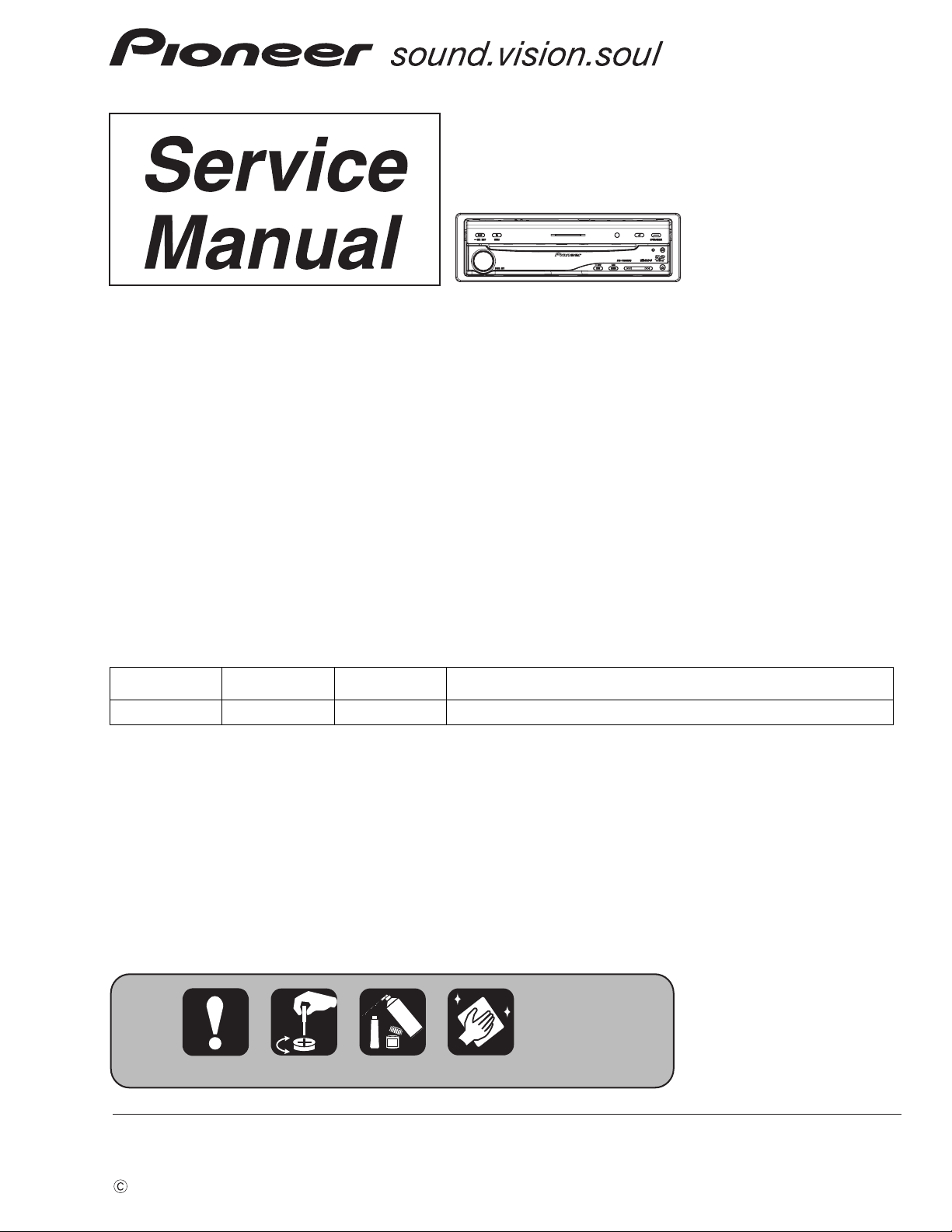
DVD AV RECEIVER
ORDER NO.
CRT3915
AVH-P5900DVD/XN/UC
AVH-P5900DVD
DVD RDS AV RECEIVER
AVH-P5900DVD
AVH-P5900DVD
This service manual should be used together with the following manual(s):
Model No. Order No. Mech.Module Remarks
CX-3212 CRT3896 MS5 DVD Mech. Module : Circuit Descriptions, Mech. Descriptions, Disassembly
"DTS" and "DTS Digital Surround" are registered trademarks of Digital Theater Systems,Inc.
Dolby noise reduction manufactured under license from Dolby Laboratories Licensing Corporation.
/XNEW5
/XN/RE
/XN/UC
"Dolby" and the double-D symbol are trademarks of Dolby Laboratories Licensing Corporation.
For details, refer to "Important Check Points for Good Servicing".
PIONEER CORPORATION 4-1, Meguro 1-chome, Meguro-ku, Tokyo 153-8654, Japan
PIONEER ELECTRONICS (USA) INC. P.O. Box 1760, Long Beach, CA 90801-1760, U.S.A.
PIONEER EUROPE NV Haven 1087, Keetberglaan 1, 9120 Melsele, Belgium
PIONEER ELECTRONICS ASIACENTRE PTE. LTD. 253 Alexandra Road, #04-01, Singapore 159936
PIONEER CORPORATION 2007
K-ZZU. MAY 2007 Printed in Japan
Page 2
1234
SAFETY INFORMATION
CAUTION
A
This service manual is intended for qualified service technicians; it is not meant for the casual do-it-yourselfer.
Qualified technicians have the necessary test equipment and tools, and have been trained to properly and safely repair
complex products such as those covered by this manual.
Improperly performed repairs can adversely affect the safety and reliability of the product and may void the warranty.
If you are not qualified to perform the repair of this product properly and safely, you should not risk trying to do so
and refer the repair to a qualified service technician.
WARNING
This product contains lead in solder and certain electrical parts contain chemicals which are known to the state of
California to cause cancer, birth defects or other reproductive harm.
Health & Safety Code Section 25249.6 - Proposition 65
B
This product contains mercury. Disposal of this material may be regulated due to environmental considerations.
For disposal or recycling information, please contact your local authorities or the Electronics Industries
Alliance: www.eiae.org.
The backlighting lamp of LCD in this equipment contains mercury. Disposal of this material may be
regulated due to environmental considerations according to Local, State or Federal Laws. For disposal
or recycling information, please contact your local authorities or the Electronics Industries
Alliance: www.eiae.org
1. Safety Precautions for those who Service this Unit.
C
D
Follow the adjustment steps in the service manual when servicing this unit. When check ing or adjusting the emitting power of the laser diode exercise caution in order to get safe, reliable results.
Caution:
1. During repair or tests, minimum distance of 13 cm from the focus lens must be kept.
2. During repair or tests, do not view laser beam for 10 seconds or longer .
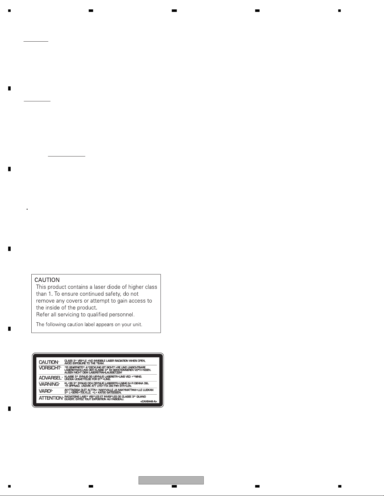
2. The triangular label is attached to the mechanism
unit frame.
On the top of the player.
E
F
2
1234
AVH-P5900DVD/XN/UC
Page 3
5 678
WARNING!
The AEL (accessible emission level )of the laser power output is less than CLASS 1
but the laser component is capable of emitting radiation exceeding the limit for
CLASS 1.
A specially instructed person should do servicing operation of the apparatus.
Laser diode characteristics
Wave length:
DVD:640 nm to 660 nm
CD:770 nm to 810 nm
DVD : 2.48 mW(Emitting period :9 sec.)
CD : 705 W(Emitting period : unlimited)
Additional Laser Caution
Transistors Q1101 and Q1102 in PCB drive the laser diodes for DVD and CD
respectively. When Q1101 or Q1102 is shorted between their terminals,
the laser diodes for DVD or CD will radiate beam. If the top cover is removed
with no disc loaded while such short-circuit is continued, the naked eyes may
be exposed to the laser beam.
A
B
C
CAUTION
Danger of explosion if battery is incorrectly replaced.
Replaced only with the same or equivalent type recommended by the manufacture.
Discord used batteries according to the manufacture's instructions.
D
E
56
AVH-P5900DVD/XN/UC
F
7
8
3
Page 4
1234
[Important Check Points for Good Servicing]
In this manual, procedures that must be performed during repairs are marked with the below symbol.
Please be sure to confirm and follow these procedures.
A
B
C
D
1. Product safety
Please conform to product regulations (such as safety and radiation regulations), and maintain a safe servicing environment by
following the safety instructions described in this manual.
1 Use specified parts for repair.
Use genuine parts. Be sure to use important parts for safety.
2 Do not perform modifications without proper instructions.
Please follow the specified safety methods when modification(addition/change of parts) is required due to interferences such as
radio/TV interference and foreign noise.
3 Make sure the soldering of repaired locations is properly performed.
When you solder while repairing, please be sure that there are no cold solder and other debris.
Soldering should be finished with the proper quantity. (Refer to the example)
4 Make sure the screws are tightly fastened.
Please be sure that all screws are fastened, and that there are no loose screws.
5 Make sure each connectors are correctly inserted.
Please be sure that all connectors are inserted, and that there are no imperfect insertion.
6 Make sure the wiring cables are set to their original state.
Please replace the wiring and cables to the original state after repairs.
In addition, be sure that there are no pinched wires, etc.
7 Make sure screws and soldering scraps do not remain inside the product.
Please check that neither solder debris nor screws remain inside the product.
8 There should be no semi-broken wires, scratches, melting, etc. on the coating of the power cord.
Damaged power cords may lead to fire accidents, so please be sure that there are no damages.
If you find a damaged power cord, please exchange it with a suitable one.
9 There should be no spark traces or similar marks on the power plug.
When spark traces or similar marks are found on the power supply plug, please check the connection and advise on secure
connections and suitable usage. Please exchange the power cord if necessary.
a Safe environment should be secured during servicing.
When you perform repairs, please pay attention to static electricity, furniture, household articles, etc. in order to prevent injuries.
Please pay attention to your surroundings and repair safely.
2. Adjustments
To keep the original performance of the products, optimum adjustments and confirmation of characteristics within specification.
Adjustments should be performed in accordance with the procedures/instructions described in this manual.
3. Lubricants, Glues, and Replacement parts
Use grease and adhesives that are equal to the specified substance.
E
Make sure the proper amount is applied.
4. Cleaning
For parts that require cleaning, such as optical pickups, tape deck heads, lenses and mirrors used in projection monitors, proper
cleaning should be performed to restore their performances.
5. Shipping mode and Shipping screws
To protect products from damages or failures during transit, the shipping mode should be set or the shipping screws should be
installed before shipment. Please be sure to follow this method especially if it is specified in this manual.
F
4
1234
AVH-P5900DVD/XN/UC
Page 5

5 678
CONTENTS
SAFETY INFORMATION .....................................................................................................................................2
1. SERVICE PRECAUTIONS................................................................................................................................6
2. SPECIFICATIONS.............................................................................................................................................8
2.1 SPECIFICATIONS ......................................................................................................................................8
2.2 DISC/CONTENT FORMAT .......................................................................................................................11
2.3 PANEL FACILITIES ..................................................................................................................................12
2.4 CONNECTION DIAGRAM........................................................................................................................14
3. BASIC ITEMS FOR SERVICE........................................................................................................................15
3.1 CHECK POINTS AFTER SERVICING .....................................................................................................15
3.2 PCB LOCATIONS.....................................................................................................................................16
3.3 JIG CONNECTION DIAGRAM .................................................................................................................17
4. BLOCK DIAGRAM ..........................................................................................................................................20
5. DIAGNOSIS ....................................................................................................................................................33
5.1 OPERATIONAL FLOW CHART................................................................................................................33
5.2 CONNECTOR FUNCTION DESCRIPTION .............................................................................................34
5.3 BACK END SECTION FLOW...................................................................................................................35
6. SERVICE MODE.............................................................................................................................................57
6.1 DVD TEST MODE ....................................................................................................................................57
7. DISASSEMBLY...............................................................................................................................................61
8. EACH SETTING AND ADJUSTMENT............................................................................................................68
8.1 DVD ADJUSTMENT.................................................................................................................................68
8.2 VIDEO LEVEL ADJUSTMENT .................................................................................................................73
8.3 MOTHER UNIT ADJUSTMENT................................................................................................................75
8.4 INVERTER ADJUSTMENT ......................................................................................................................77
8.5 MONITOR ADJUSTMENT........................................................................................................................79
8.6 MONITOR TEST MODE...........................................................................................................................85
8.7 CALIBRATION TEST ................................................................................................................................91
9. EXPLODED VIEWS AND PARTS LIST ........................................................................................................100
9.1 PACKING................................................................................................................................................100
9.2 EXTERIOR(1).........................................................................................................................................104
9.3 EXTERIOR(2).........................................................................................................................................106
9.4 EXTERIOR(3).........................................................................................................................................110
9.5 EXTERIOR(4).........................................................................................................................................112
9.6 DVD MECHANISM MODULE.................................................................................................................114
10. SCHEMATIC DIAGRAM.............................................................................................................................. 116
10.1 MOTHER UNIT(SYSTEM PART)(GUIDE PAGE)................................................................................. 116
10.2 MOTHER UNIT(POWER SUPPLY PART)(GUIDE PAGE) ...................................................................122
10.3 KEYBOARD UNIT ................................................................................................................................128
10.4 MONITOR PCB(MONITOR PART)(GUIDE PAGE) ..............................................................................130
10.5 MONITOR PCB(OSD & µCON PART)(GUIDE PAGE).........................................................................136
10.6 DVD CORE UNIT(1/2)(GUIDE PAGE) .................................................................................................142
10.7 DVD CORE UNIT(2/2)..........................................................................................................................148
10.8 COMPOUND UNIT(A) AND COMPOUND UNIT(B).............................................................................150
10.9 RCA PCB..............................................................................................................................................151
10.10 UPPER PCB.......................................................................................................................................152
10.11 OPT PCB ............................................................................................................................................153
10.12 MAIN PCB UNIT(SERVICE), SWITCH PCB UNIT AND VOLUME PCB UNIT ..................................154
10.13 WAVEFORMS.....................................................................................................................................156
11. PCB CONNECTION DIAGRAM ..................................................................................................................158
11.1 MOTHER UNIT .....................................................................................................................................158
11.2 KEYBOARD UNIT.................................................................................................................................162
11.3 MONITOR PCB.....................................................................................................................................164
11.4 DVD CORE UNIT..................................................................................................................................168
11.5 COMPOUND UNIT(A) AND COMPOUND UNIT(B) .............................................................................172
11.6 RCA PCB ..............................................................................................................................................173
.......174
11.7 UPPER PCB .......................................................................................................................
11.8 OPT PCB ..............................................................................................................................................175
11.9 MAIN PCB UNITSERVICE), SWITCH PCB UNIT AND VOLUME PCB UNIT......................................176
12. ELECTRICAL PARTS LIST.........................................................................................................................177
...........
A
B
C
D
E
56
AVH-P5900DVD/XN/UC
F
7
8
5
Page 6

1234
1. SERVICE PRECAUTIONS
- Service Precautions
1) You should conform to the regulations governing the product (safety, radio and noise, and other regulations),
A
and should keep the safety during servicing by following the safety instructions described in this manual.
2) Be careful in handling ICs. Some ICs such as MOS type are so fragile that they can be damaged by electrostatic
induction.
3) Before disassembling the unit, be sure to turn off the power. Unplugging and plugging the connectors
during power-on mode may damage the ICs inside the unit.
4)To protect the pickup unit from electrostatic discharge du rin g s ervicing, take an appropriate treatment
(shorting-solder) by referring to "the DISASSEMBLY" .
5) After replacing the pickup unit, be sure to skew adjustment.
6)During disassembly, be sure to turn the power off since an internal IC might be destroyed when a connector
is plugged or unplugged.
7) In case the internal fuse has blown, check the voltage of the rear stage.
8) Handling instructions for touch panel
Please handle the touch panel with care as it contains glass.
Dropping or giving a strong shock may break the panel.
B
Wear gloves, etc. to protect your hands from the glass edges that are not deburred.
9) Remove a small board (2 screws) provided for pulling out an RCA line, before removing the mother board.
10) Hot areas
Red area: Hot area. Be careful not to burn yourself
Moter Unit(Side A)
Moter Unit(Side B)
C
Red-circled area: The heat from hot parts on the B-side of the board is removed from the product bottom through a heat
transfer sheet.
D
Be careful not to burn yourself with the hot area.
Bottom
E
is a trademark of DVD Format/Logo Licensing Corporation.
F
6
1234
AVH-P5900DVD/XN/UC
Page 7

5 678
NOTES ON SOLDERING
For environmental protection, lead-free solder is used on the printed circuit boards mounted in this unit.
Be sure to use lead-free solder and a soldering iron that can meet specifications for use with lead-free solders for repairs
accompanied by reworking of soldering.
Compared with conventional eutectic solders, lead-free solders have higher melting points, by approximately 40 C.
Therefore, for lead-free soldering, the tip temperature of a soldering iron must be set to around 373 C in general, although
the temperature depends on the heat capacity of the PC board on which reworking is required and the weight of the tip of
the soldering iron.
Compared with eutectic solders, lead-free solders have higher bond strengths but slower wetting times and higher melting
temperatures (hard to melt/easy to harden).
The following lead-free solders are available as service parts:
Parts numbers of lead-free solder:
GYP1006 1.0 in dia.
GYP1007 0.6 in dia.
GYP1008 0.3 in dia.
A
B
C
D
E
56
AVH-P5900DVD/XN/UC
F
7
8
7
Page 8
1234
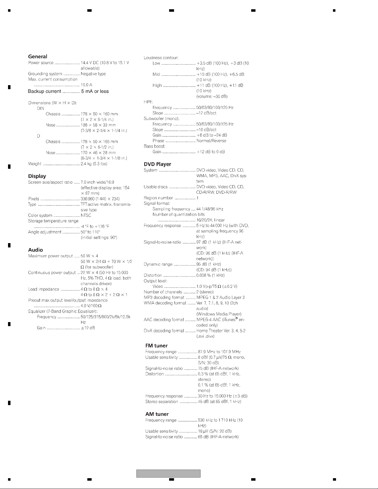
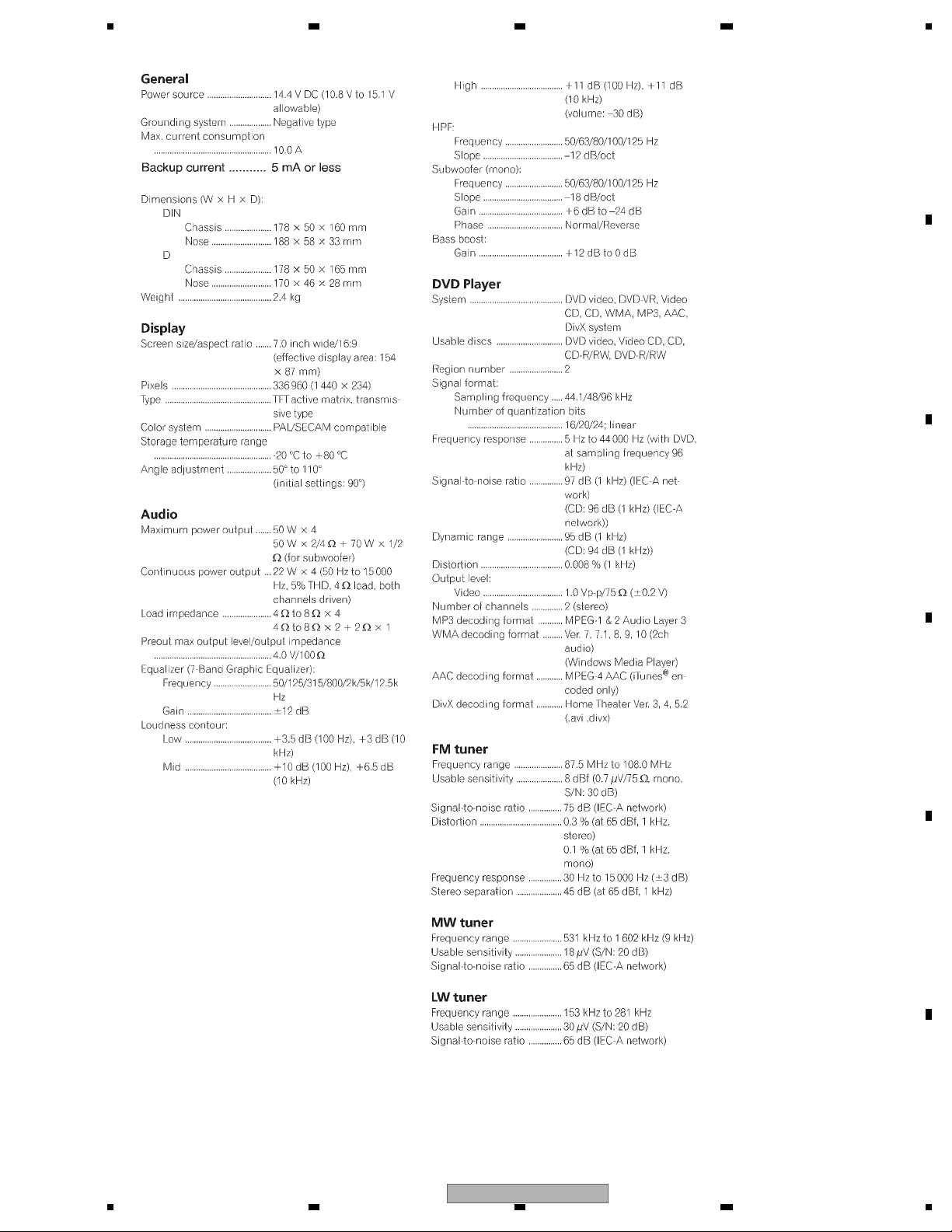
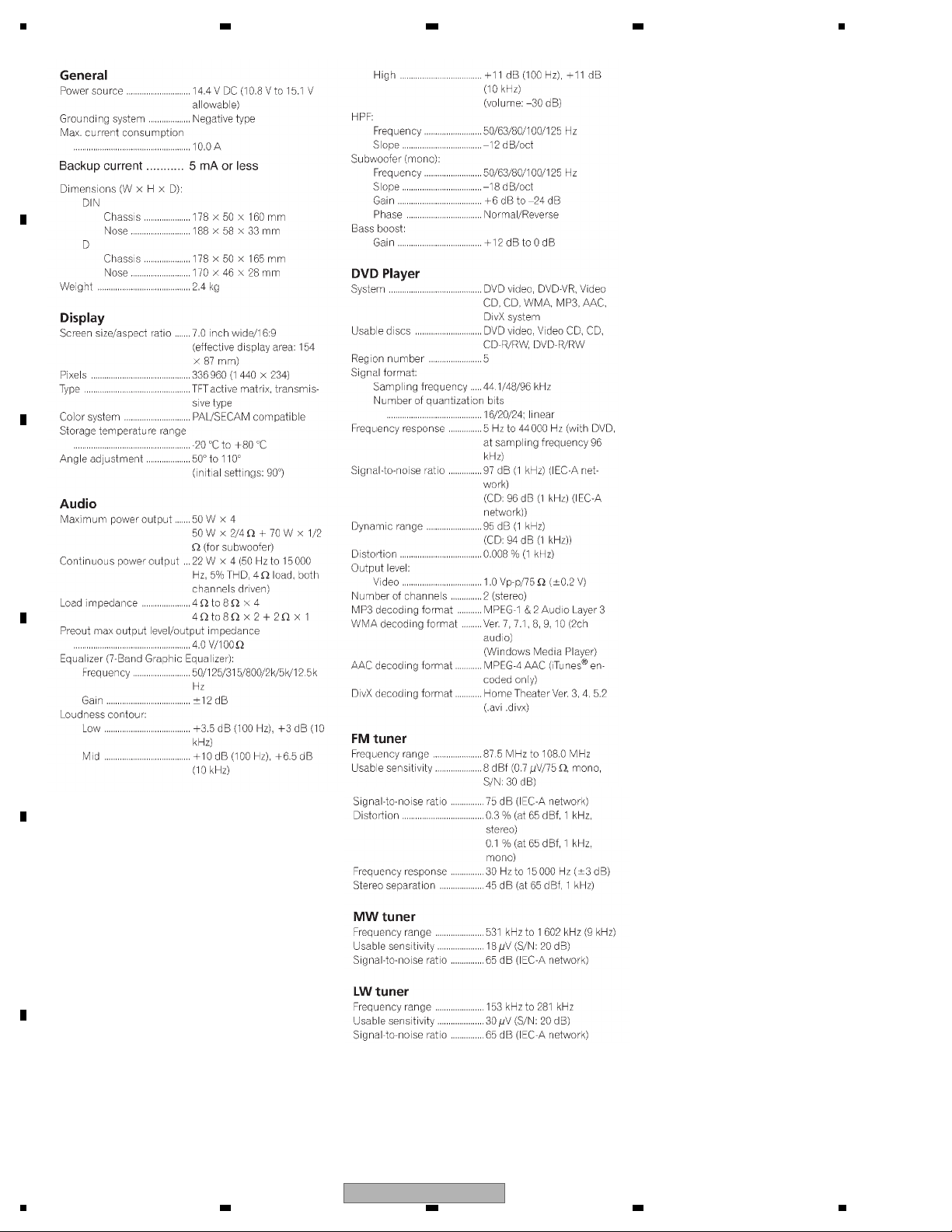
2. SPECIFICATIONS
2.1 SPECIFICATIONS
- AVH-P5900DVD/XN/UC
A
B
C
D
E
F
8
1234
AVH-P5900DVD/XN/UC
Page 9
5 678
- AVH-P5900DVD/XNEW5
A
B
C
D
E
56
AVH-P5900DVD/XN/UC
F
7
8
9
Page 10
1234
- AVH-P5900DVD/XN/RE
A
B
C
D
E
F
10
1234
AVH-P5900DVD/XN/UC
Page 11
5 678
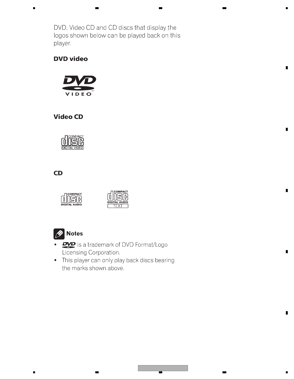
2.2 DISC/CONTENT FORMAT
A
B
C
D
E
56
AVH-P5900DVD/XN/UC
F
7
8
11
Page 12
1234
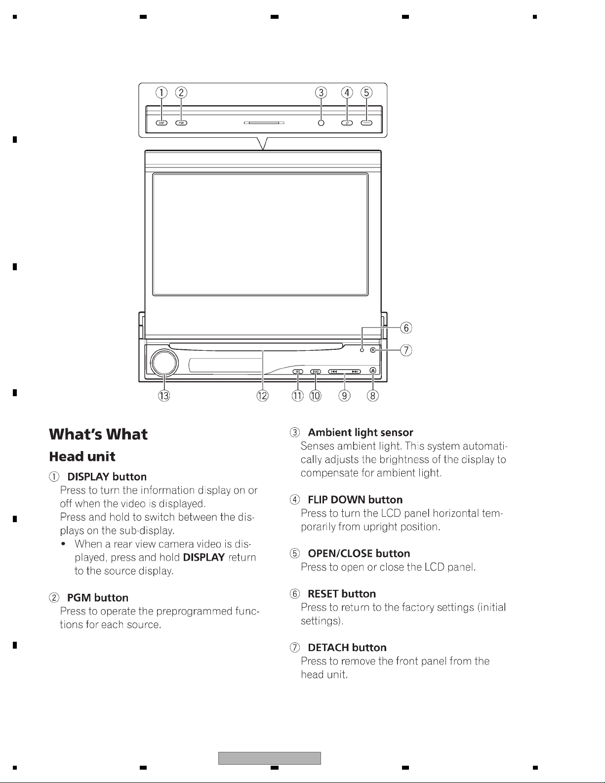
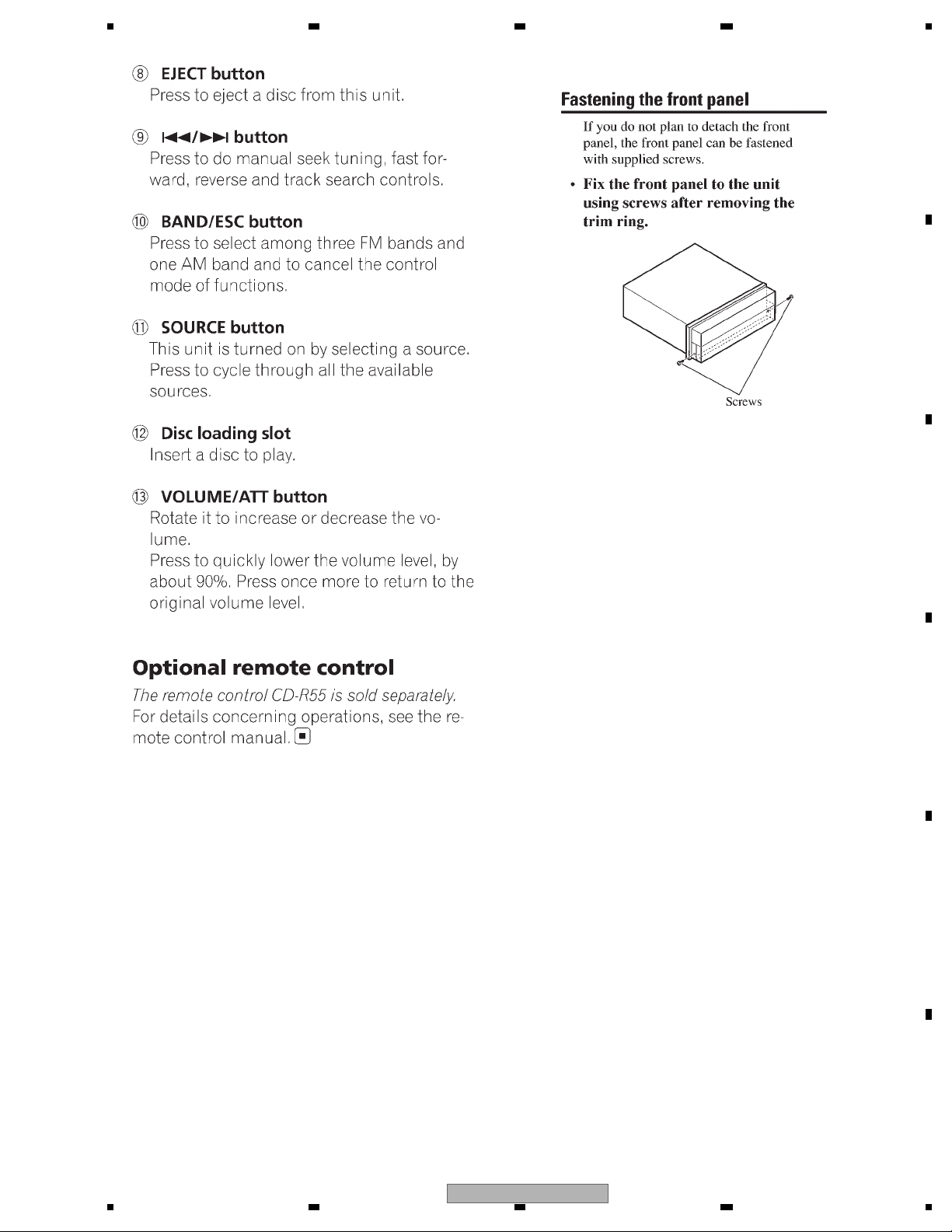
2.3 PANEL FACILITIES
A
B
C
D
E
F
12
1234
AVH-P5900DVD/XN/UC
Page 13
5 678
A
B
JGZ20P070FTC
C
D
E
56
AVH-P5900DVD/XN/UC
F
7
8
13
Page 14
1234
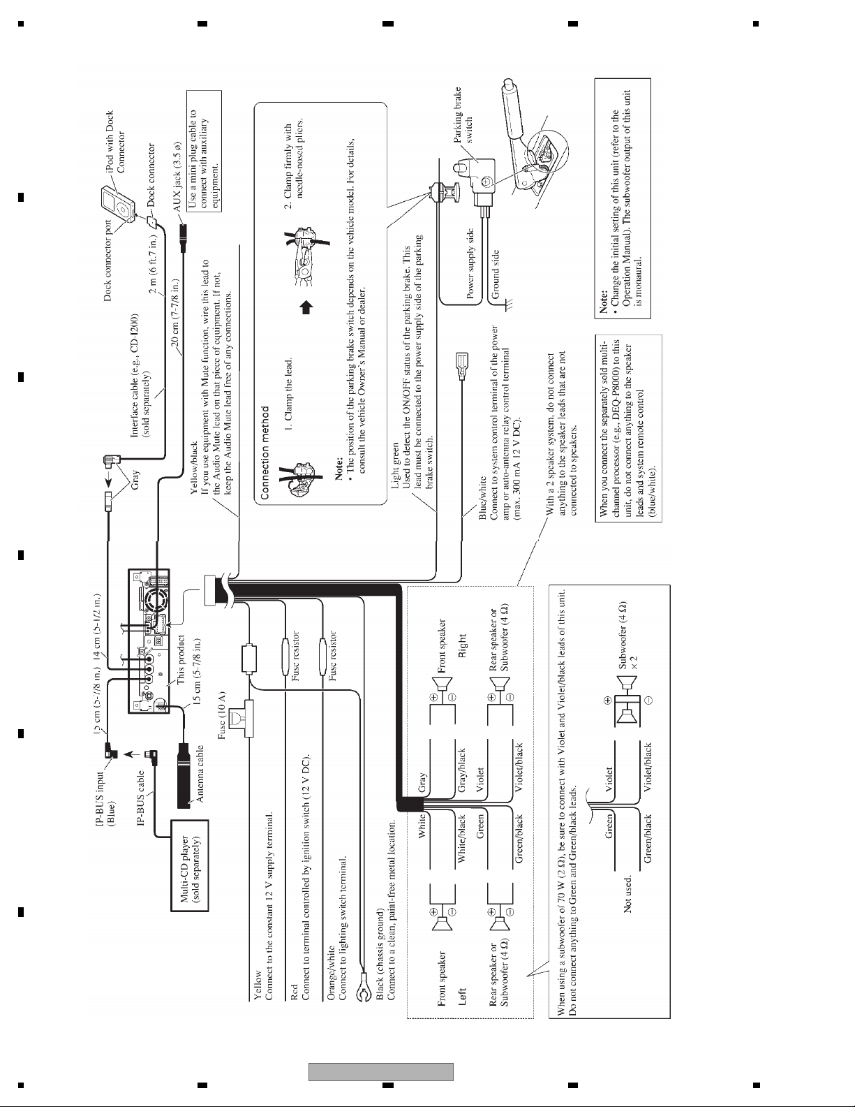
2.4 CONNECTION DIAGRAM
- Connection Diagram
A
B
C
D
E
F
14
1234
AVH-P5900DVD/XN/UC
Page 15
5 678
g
p
(
)
(
)
S
(
)
j
g
g
g
g
g
3. BASIC ITEMS FOR SERVICE
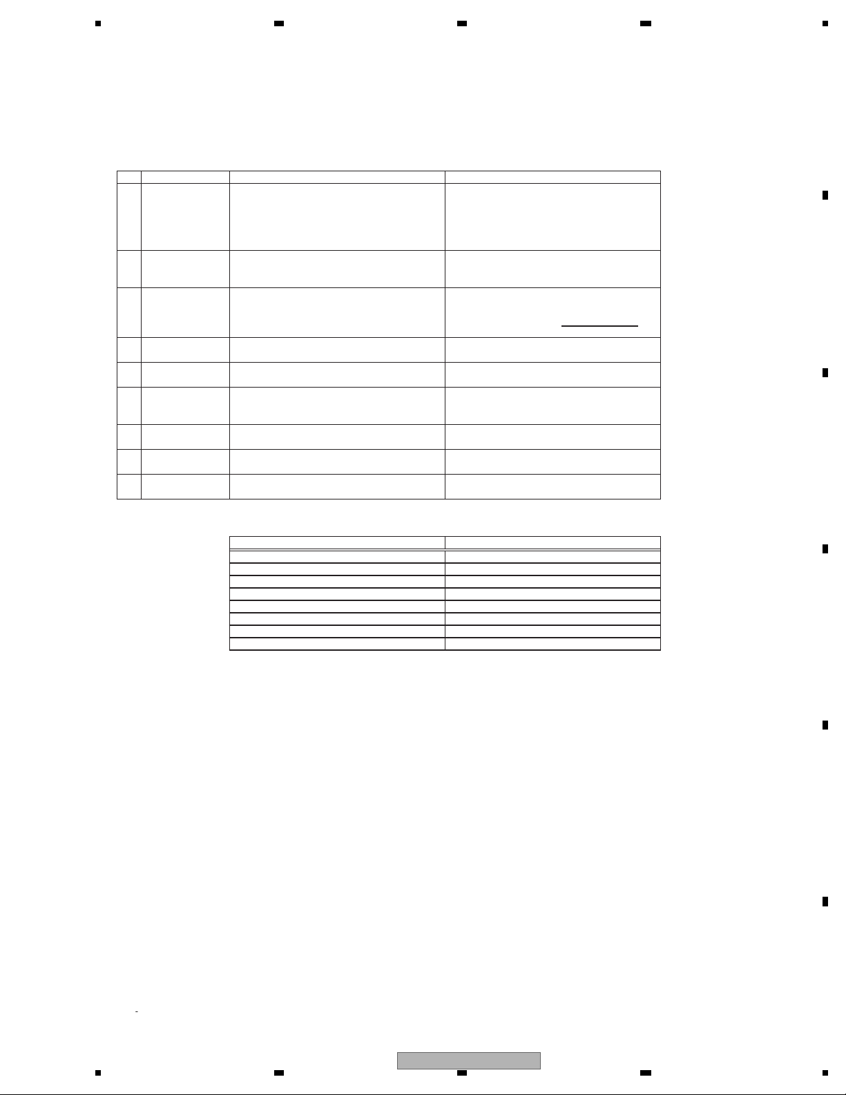
3.1 CHECK POINTS AFTER SERVICING
CHECK POINTS AFTER SERVICING (AVH)
A
To keep the product quality after servicin
1 Confirm whether the customer complain has
2 Flap-mecha Check the operation of the flap mechanism. The flap mechanism operation must be
3 DVD Measure playback error rates at the
4 DVD Play back a DVD.
5 CD Play back a CD.
6 FM/AM tuner Check FM/AM tuner action.
7 TV tuner Check TV tuner action.
8 Check whether no disc is inside the product. The media used for the operating check
See the table below for the items to be checked re
been solved.
If the customer complain occurs with the
specific media, use it for the operation
check.
innermost and outermost tracks by using the
test mode with the following disc.
Menu operation;Title/chapter search
Track search
(Seek, Preset)
witch band to check both FM and AM.
Seek;Preset
Item to be checked regarding video Item to be checked regarding audio
Disturbed ima
Too bri
Mottled color
, please confirm followingcheck points.
kcehCserudecorP.oN
The customer complain must not be
reappeared.
Display, video, audio and operations must
be normal.
smooth without making
scratches.
Deterioration of mecha-drive can be
checked.
The error rates must be less than 2.5e-4
Display, video, audio and operations must
be normal.
Display, audio and operations must be
normal.
Display, audio and operations must be
normal.
Display, video, audio and operations must
be normal.
must be e
receivin
ardingvideo and audio:
e (video jumpiness) Volume too high
ected.
it for service.
noitrotsiDesion-kcolB
esioNesionlatnoziroH
wolootemuloVesiontoD
the noise and
nitautculfemuloVkradooT
detpurretnidnuoSth
krameRstnio
When flap-mecha
exists
B
.
C
retfaecnaraeppastinotridrosehctarcsoNkcehcecnaraeppA9
D
E
F
AVH-P5900DVD/XN/UC
56
7
8
15
Page 16
1234
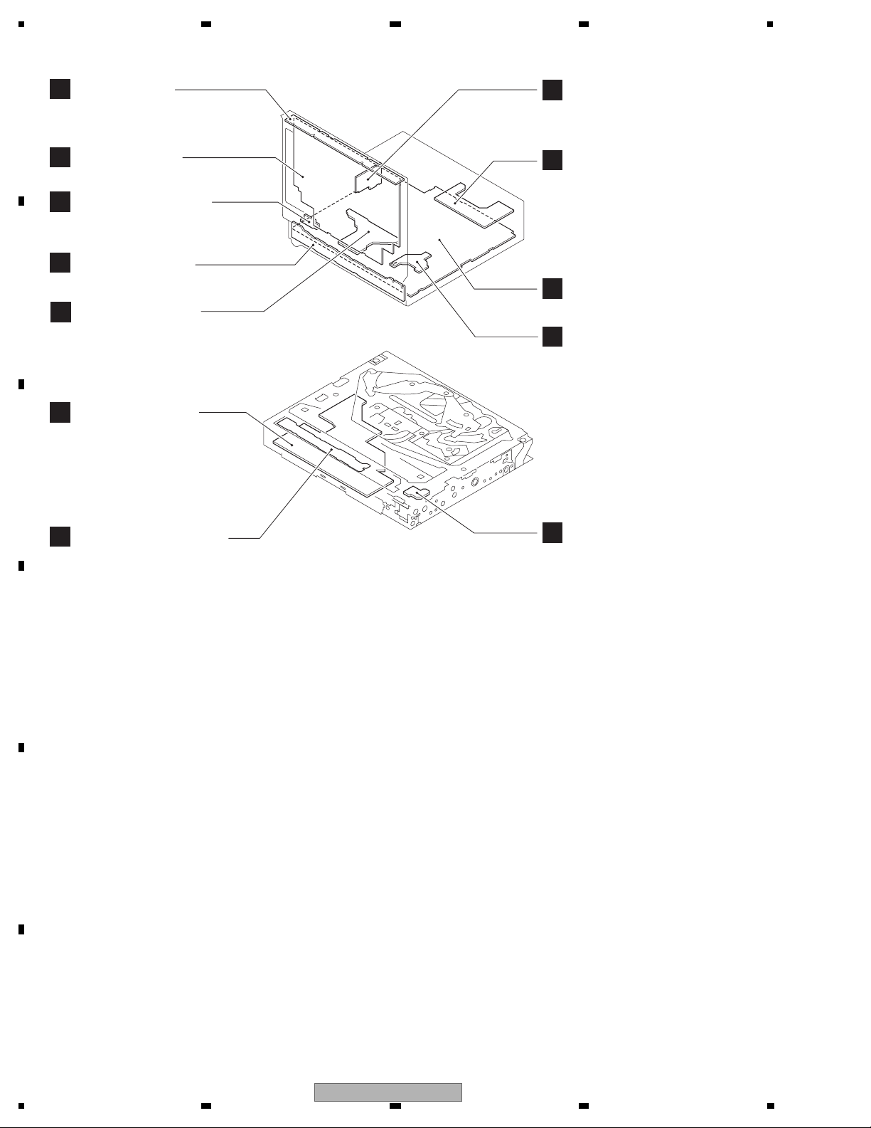
3.2 PCB LOCATIONS
Upper PCB
H
A
Monitor PCB
C
Switch PCB Unit
K
B
Keyboard Unit
B
Main PCB Unit
J
(SERVICE)
DVD Core Unit
D
C
RCA PCB
G
OPT PCB
I
Mother Unit
A
Volume PCB Unit
L
Compound Unit (A)
E
Unit Number : CXC7508(UC)
Unit Number : CXC7506(EW5)
Unit Number : CXC7507(RE)
Unit Name : DVD Amp Assy
Unit Number : CWN2330
D
Unit Name : Monitor Unit
Monitor Unit
Consists of
Monitor PCB
Upper PCB
Unit Number : YWX5005
Unit Name : DVD Core Unit
Unit Number : CWX3154
Unit Name : Compound Unit(A)
Unit Number : CWX3394
Unit Name : Compound Unit(B)
E
Compound Unit (B)
F
DVD Amp Assy
Consists of
Mother Unit
OPT PCB
RCA PCB
Unit Number : CXX2316
Unit Name : Main PCB Unit(SERVICE)
Unit Number : CZW5029
Unit Name : Switch PCB Unit
Unit Number : CZW5028
Unit Name : Volume PCB Unit
F
16
1234
AVH-P5900DVD/XN/UC
Page 17
5 678
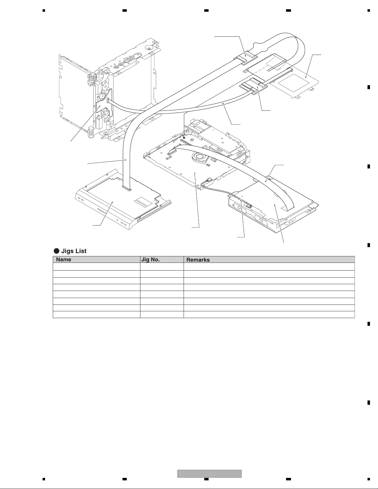
3.3 JIG CONNECTION DIAGRAM
Main PCB Unit
GGF1462
33-Pin Relay PCB
GGD1209
20-Pin FFC
A
Bracket
GGF1461
40-Pin + 20-Pin Relay PCB
B
GGD1262
33-Pin FFC
Monitor PCB
Mother Unit
GGD1284
40-Pin FFC BBR
Cord
CDE8384
40-Pin FFC BBR GGD1284 DVD Mechanism Module <--> DVD Amp Assy
33-Pin Relay PCB GGF1462 DVD Amp Assy <--> Monitor Unit
33-Pin FFC GGD1262 DVD Amp Assy <--> Monitor Unit
40-Pin + 20-Pin Relay PCB GGF1461 DVD Amp Assy <--> Main PCB Unit
20-Pin FFC GGD1209 DVD Amp Assy <--> Main PCB Unit
Disc GGV1018 Skew adjustment
TORX driver(T2) GGK1095 Skew adjustment
Bond GEM1033 Skew adjustment
DVD Mechanism Module
C
D
56
AVH-P5900DVD/XN/UC
E
F
7
8
17
Page 18
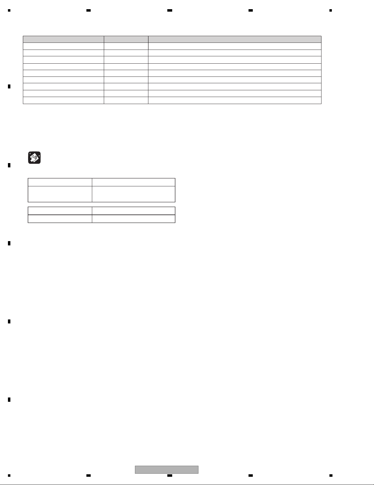
- Grease List
Name
A
B
C
Grease
Grease
Grease
Grease
Locking agents
Grease
Grease
Grease
Grease
Before shipping out the product, be sure to clean the following portions by using the prescribed cleaning tools:
1234
Jig No.
GEM1024
GEM1043
GEM1045
GEM1050
1401M
GEM1011
GEM1047
GEM1071
GEM1072
Remarks
DVD Mechanism Module and Chassis
DVD Mechanism Module and Chassis
DVD Mechanism Module
DVD Mechanism Module
DVD Mechanism Module (1401M:produced by THREE BOND)
Chassis
Chassis
Chassis
Chassis
CLEANING
Portions to be cleaned Cleaning tools
DVD pickup lenses Cleaning liquid : GEM1004
Cleaning paper : GED-008
Portions to be cleaned Cleaning tools
Fans Cleaning paper : GED-008
D
E
F
18
AVH-P5900DVD/XN/UC
1234
Page 19

5 678
A
B
C
D
E
56
AVH-P5900DVD/XN/UC
F
7
8
19
Page 20
1234
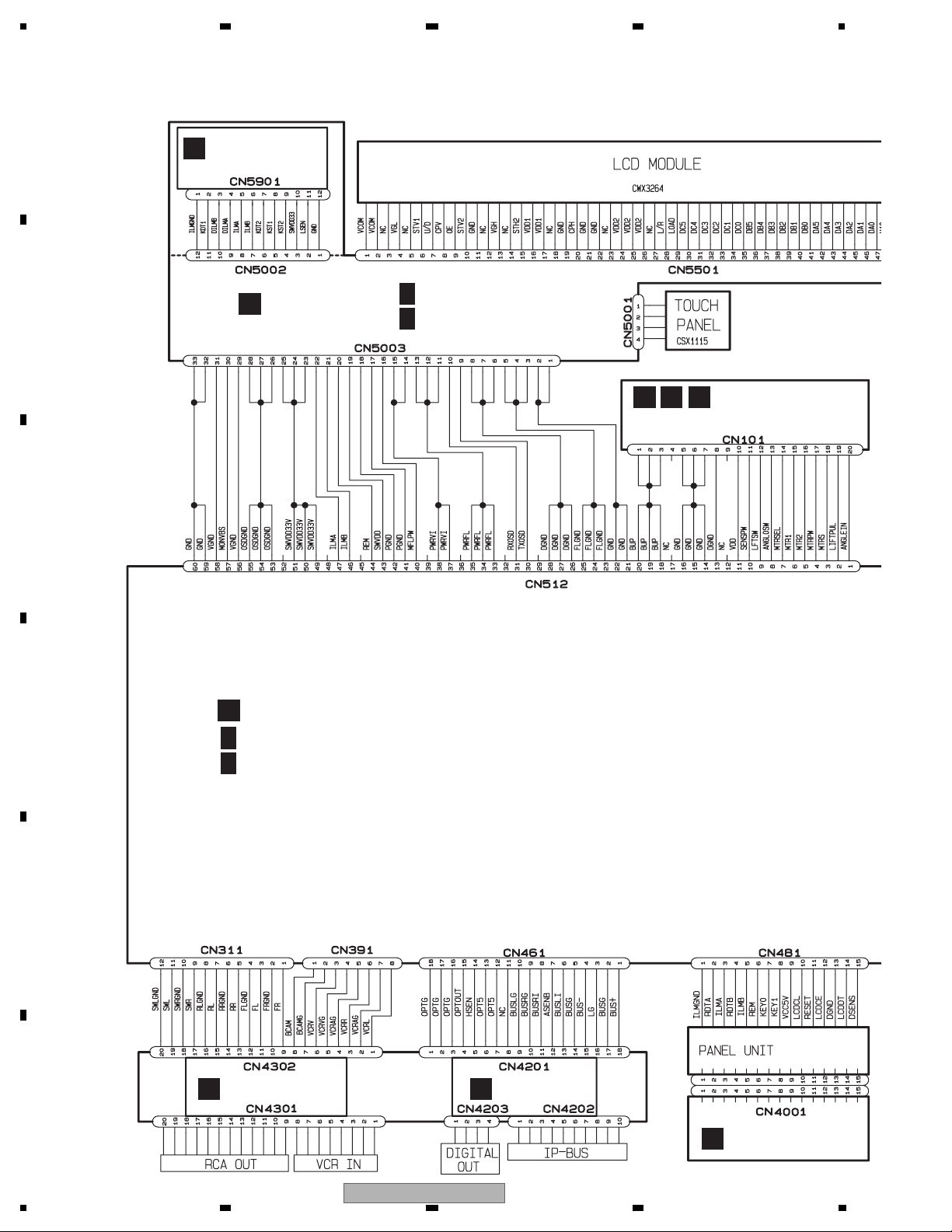
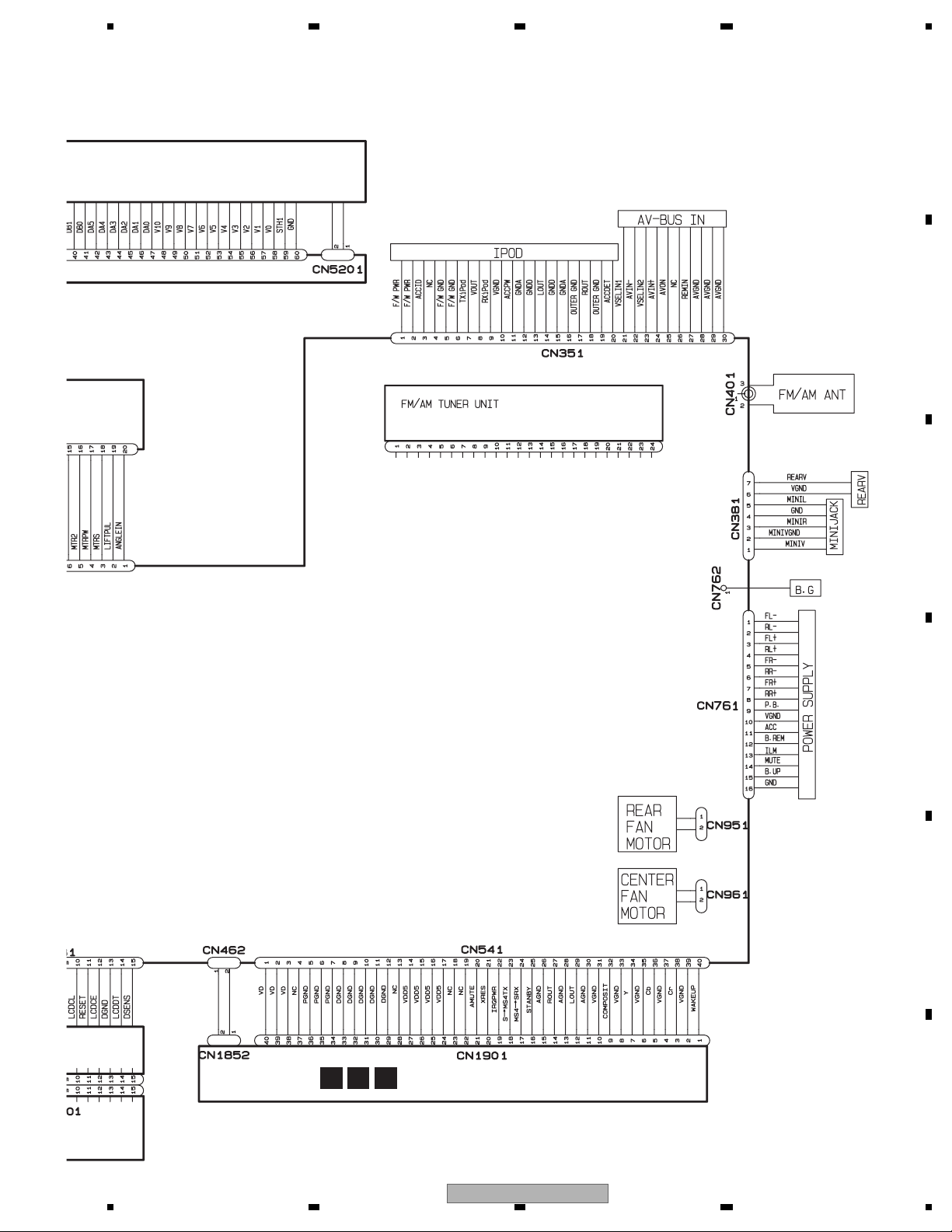
4. BLOCK DIAGRAM
A
UPPER PCB
H
B
C
MONITOR PCB
MONITOR PART
1/2
C
OSD & CON PART
2/2
C
μ
J K L
C
MOTHER UNIT
D
A
SYSTEM PART
1/2
A
POWER SUPPLY PART
2/2
A
DRIVE UNIT
E
RCA PCB
G
F
20
1234
AVH-P5900DVD/XN/UC
OPT PCB
I
KEYBOARD UNIT
B
Page 21
IT
5 678
A
B
C
D
E
RD UNIT
D E F
DVD MECHANISM MODULE
AVH-P5900DVD/XN/UC
56
F
7
8
21
Page 22
1234
V
V
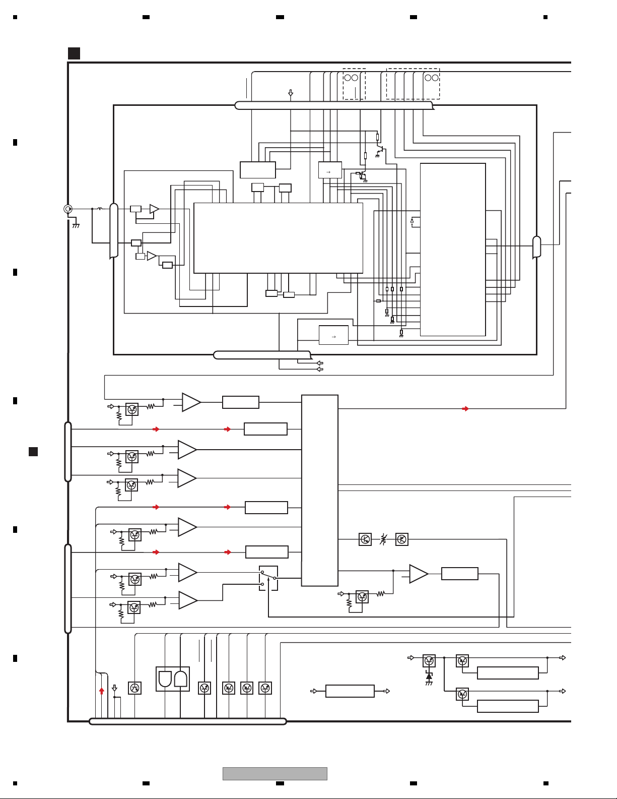
MOTHER UNIT (1/2)
A
A
TUNPCK
TUNPCE
CK
CE1
B
LDET
TUNPDI
RDS_CK
DO
LDET
RDS_CK
A
TUNPCE2
76 13 51098 11 1418192021
NC
CE2
VDD33
ROM_VDD
TUNSL
SL
TUNPDO
DI
RDS_DATA
RDS_DATA
A
RDS_LOCK
RDS_HSLK
RDS_HSLK
RDS_LOCK
B
B
C
D
E
CN4302
G
MINI JACK/
REARV
CN401
2,3
CN391
8
3
1
CN381
5
1
7
1
VCRL
VCRV
BCAM
MINIL
MINIV
REARV
VIDEO5
VIDEO5
VIDEO5
LOUT
VOUT
VIDEO5
AVIN +
VIDEO5
VIDEO5
AM ANT
1
FM ANT
3
COMPOSIT
ATT
ATT
ANT adj
FMRF
FMRF
RF adj
Q191
Q161
Q181
Q111
Q231
Q141
MECHA VIDEO ISO
IC191
NJM2136V
3
+
6
2
-
VCR VIDEO ISO
3
2
3
2
3
2
3
2
NJM2136V
+
6
-
B.CAMERA ISO
NJM2136V
+
6
-
iPod VIDEO ISO
NJM2136V
+
6
-
AV-BUS VIDEO ISO
NJM2136V
+
6
-
3
+
6
2
MINIJACK VIDEO ISO
IC231
IC 3 EEPROM
5.0V
OSC
LPF
IC 1
3.3V
MIXER, IF AMP
T51
RFGND
OSCGND
DGND
BUFFER
IC192
SM5304AV
AUDIOGNDNCVCC
61
212 1522 16 4 17
212 1522 16 4 17
VCR AUDIO ISO
IC151
NJM2794RB2
IC161
IC181
iPod AUDIO ISO
10
IC101
IC111
NJM2794RB2
MINIJACK AUDIO ISO
IC131
NJM2794RB2
1
7
3
2
AV-B US&
MINI VIDEO SW
IC141
NJM2136V
NJM2233BM
CF52
VDD_3.3
AV SELECTOR
43
13
110
44
45
17
1
46
19
110
47
IC221
5V 3.3V
3.3V 2.5V
3.3V
IC241
AN15883A
V1
LOUT1
L2
V2
V3
L4
V4
VOUT1
L5
VOUT2
V5
VIDEO9
IC 5
IC 2
2.5V
DET, FM MPX,
RDS DECODER
IC 4
2.5V
TUN33V
TUN+B
23 AVL
36 AVSCL
SCL
35 AVSDA
SDA
MONITOR VBS BUFFER
31
30
Q251
VCRSEL
Q272VR271Q271
IC251
NJM2136V
3
+
2
-
REARV ISO&
6
DRIVER
IC252
BA7623F
MONVBS
8REARV2
Lch
VCRSEL
Lch
23
VSELIN1
IPODSENS
IP_ACCPW
71
53
FWPW
+
F/W PWR
VOUT8LOUT
CN351
AVIN
1
24
F
22
14
1234
IC351
Q351
TC7WH08FU
ACCID ACCID
2
TXiPod TXIPOD7RXiPod RXIPOD
3
Q352
ACCPW
9
ACCDET
11
iPod/AV-BUS IN
VSELIN2
TUN+B
REMIN
AVON AVON
27
25
20
Q353
VSELIN1
21
Q354
Q355
VSELIN2
23
AVH-P5900DVD/XN/UC
TUN3.3V
13
IC811
NJM2391DL1-33
TUN33V
B.UP
Q842
Q841
Q851
VDD33V
23
IC841
S-812C33AUA-C2N
VDD5
23
IC851
S-812C50AUA-C3E
Page 23
5 678
V
A-C2N
A-C3E
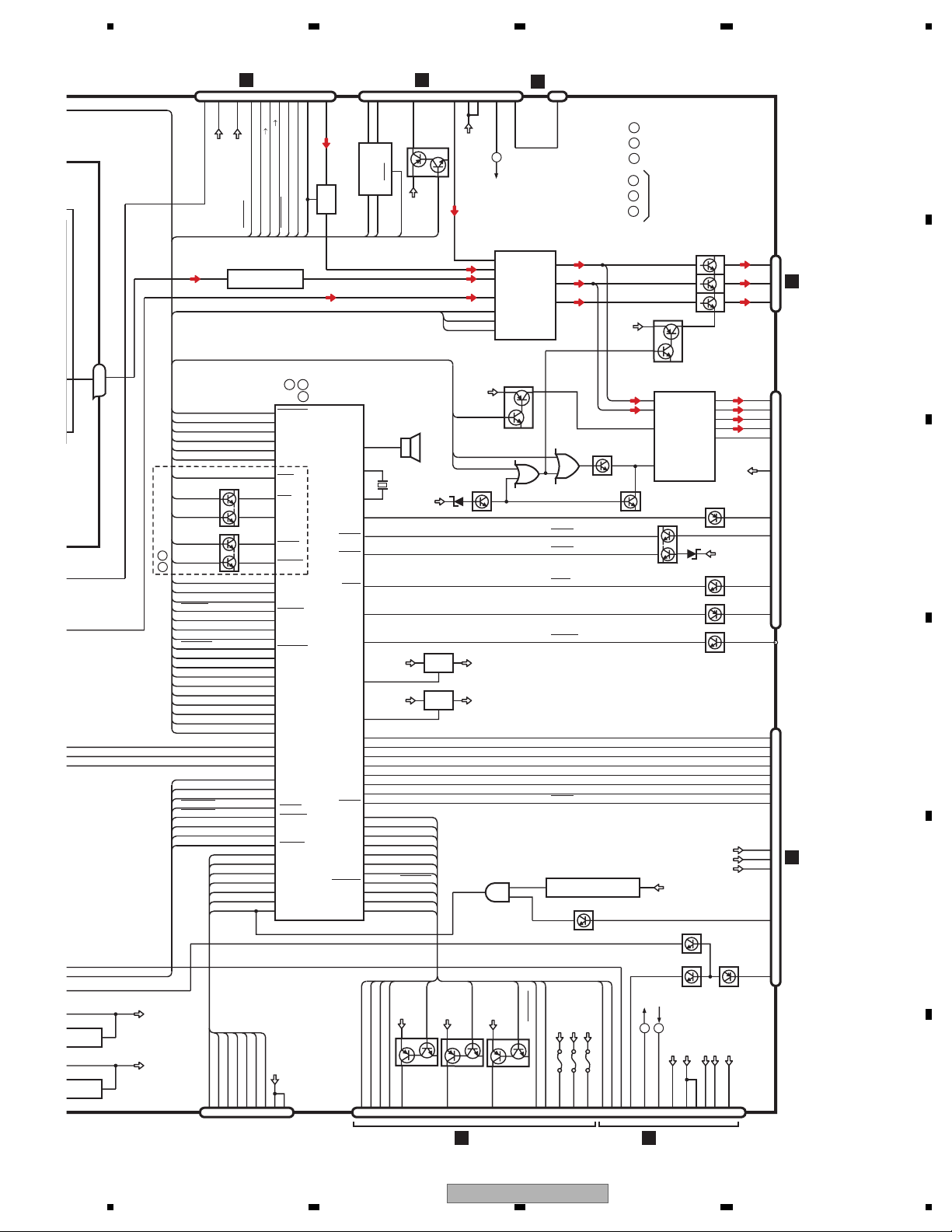
CN1901
D
I
I
3
1
32
14
VD
VDD5
CN541
COMPOSIT
VD8
VD5
TUNER AUDIO ISO
10 1
NJM2794RB2
Lch
Lch
23
Q402
RDS_CK
RDS_DATA
Q401
RDS_LOCK
A
RDS_HSLK
B
XRESET
VDD33
VDD5
REMIN
IRQPW
TXMS5
RXMS5
STANDBY
WAKEUP
AMUTE
IETX
IERX
ACCID
TXIPOD
RXIPOD
IP_ACCPW
IPODSENS
VSELIN1
VSELIN2
AVON
CN531
RESET2
DMS6DRST7RESET
DCK2FLMDO
5
AVL
3
3
21
17
XRES
XRESET
IC401
DDI8DDO
22
IRQPWRIRQPW
114
144
25
27
113
26
18
19
98
101
100
107
106
105
63
64
61
62
75
76
66
31
32
29
30
117
45
80
23
22
92VCRSEL
132
60
59
116
115
93
94
95
41
8
42
20
39
40
14
RESET2
9
25
40
24
23
AMUTE
STANBY
WAKEUP
S MS4TXTXMS5
MS4 SRXRXMS5
STANDBY
SYSTEM MICON
IC601(1/2)
A
B
C
TUNPCE2
TUNSL
TUNPDO
TUNPCK
TUNPCE
TUNPDI
LDET
RCK
RDT
RDSLK
RDS57K
EVSEL
EVSCK
EVSDA
XRESET
IRQPW
TXMS5
RXMS5
STANDBY
WAKEUP
AMUTE
TXIE
RXIE
IPPW
ASENBO
AMPPW
AMPMUTE
SYSMUTE
AVSCK
AVSD ATA
VCRSEL
PID
TXIPOD
RXIPOD
PSENS
PSENSG
VSELIN1
VSELIN2
AVONIN
DCK
FLMDO
DMS
DRST
DDI
DDO
RESET
VDD33
3.3V
4
10
11
20
LOUTMS5L
:PE5598A
:PE5597A
TELMUTEIN
1
29
Q541
Q542
BLUE_ON
LFTPULS
DEGOSW
4
BUS-
BUS+
CN461
6
5
-
+
BUS
BUS
IC461
DIN1
ROUT
HA12241FP
1
2
IETX
IERX
TUN L
52
BEEP
13
X2
12
X1
46 PBSENS
PBSENS
74
ASENS
21
BSENS
143
ISENS
82 TELIN
47 BGSENS
BGSENS
ILM+B
79
RED_ON
ILM+B
78
137
ROTIN1
136
ROTIN2
139
KEYIN1
138
KEYIN2
51
LCDCK
48
LCDCE
50
LCDDT
140
DSENS
129 ANGLE
ANGLE
17 LFTPULS
124
MTRS
122
MTRPW
126 S_MTR2
MTR2
125 S_MTR1
MTR1
123 S_MTRSEL
MTRSEL
127
77
LFTSW
35 TXMON
TXMON
36 RXMON
RXMON
ANGLEANGLEIN
LFTPULSLIFTPUL
MTRS
MTRPW
CN512
12345
7
ASENB
8
STBY
B.UP
IPPW
X601
4.718592MHz
B.UP
DEGOSW
SENS5V
MTR2
I
BZ601
S-MTR2
Q523
Q461
Q783
Q784
Q781
Q782
CN4201
BUSLI
ASENBO
SENS5V
MTR1
6
6
IPBUS+L
SYS+B
AMPPW
SYSMUTE
OFFMUTE
J
12
13
14
HSEN
OPTOUT
OPT5
D
to 2/2
E.VOL CAPTAIN7
IC281
PML017A
7
IN4+
9MS5L
IN2L
8
IN3L
10AVL
IN1L
15EVSEL
STB
16EVSCK
CLK
17EVSDA
DATA
Q331
AMPMUTE
Q743
ILMA
ILMB
IC732
TC7SET08FUS1
Q522
4
S-MTR1
CN101
SENS5V
MTRSEL
7
1
2
S-MTRSEL
Q521
CN1852
D
1
15
CN462
A
:AVH-P5900DVD/XNEW5
B
:AVH-P5900DVD/XN/RE
C
:AVH-P5900DVD/XN/UC
D
E
to 2/2
F
RCAMUTE
12
FLIN
14
RLIN
4
STBY
22
MUTE
Q765
ILMSENS
Q311
Q313
Q312
Q741
AMP
IC331
PAL007C
B.REMOTE
OUTFL
OUTRL
OUTPREL
38
39
40
ASENS
BSENS
ISENS
Q742
Q744
B.UP
FL
RL
ASENS
BSENS
TELIN
BGSENS
ROTIN1
ROTIN2
KEYIN1
KEYIN2
LCDCK
LCDCE
LCDDT
POWER ON RESET
12
IC731
S-80827CNNB-B8M
Q731
DEGOSW
SENS5V
SENS33V
FU522
FU521
FU523
LFTSW
SENSPW
ANGLOSW
VDD
BUP
9108
18
11
TXMONTXOSD
RXMONRXOSD
B.UP
MONVBS
I
20
30
REM
REMIN
MOREN
E
MFLPW
4043445731
C
VDD33
RESET1
to 2/2
to 2/2
F
SWVDD
PWRFL
33
CN5003
PWFL
I
35
Q503
Q502
PWVI
PWRVI
374647
MUTE
5
FL+
3
FL-
21
RL+
23
RL-
25
PBSENS
Q763
B.UP
Q762
Q761
Q766
ILMA
ILMB
SWVDD5
Q501
ILMB
ILMA
38
CN311
CN761
B.REM
B.UP
MUTE
CN762
CN481
RDTA
RDTB
KEY0
KEY1
LCDCL
LCDCE
LCDDT
DSENSDSENS
VCC5V
RESET
SWVDD33
SWVDD33V
I
51
49
SWL
RL+
ACC
REM
A
FL
3
RL
CN4302
7
G
11
B
FL+
3
FL-
1
4
RL-
2
12
15
POWER
SUPPLY
P. B .
9
11
ILM
13
14
C
BG
D
2
4
7
8
10
12
14
15
3
CN4001
5
B
9
11
6
E
F
56
AVH-P5900DVD/XN/UC
7
8
23
Page 24
1234
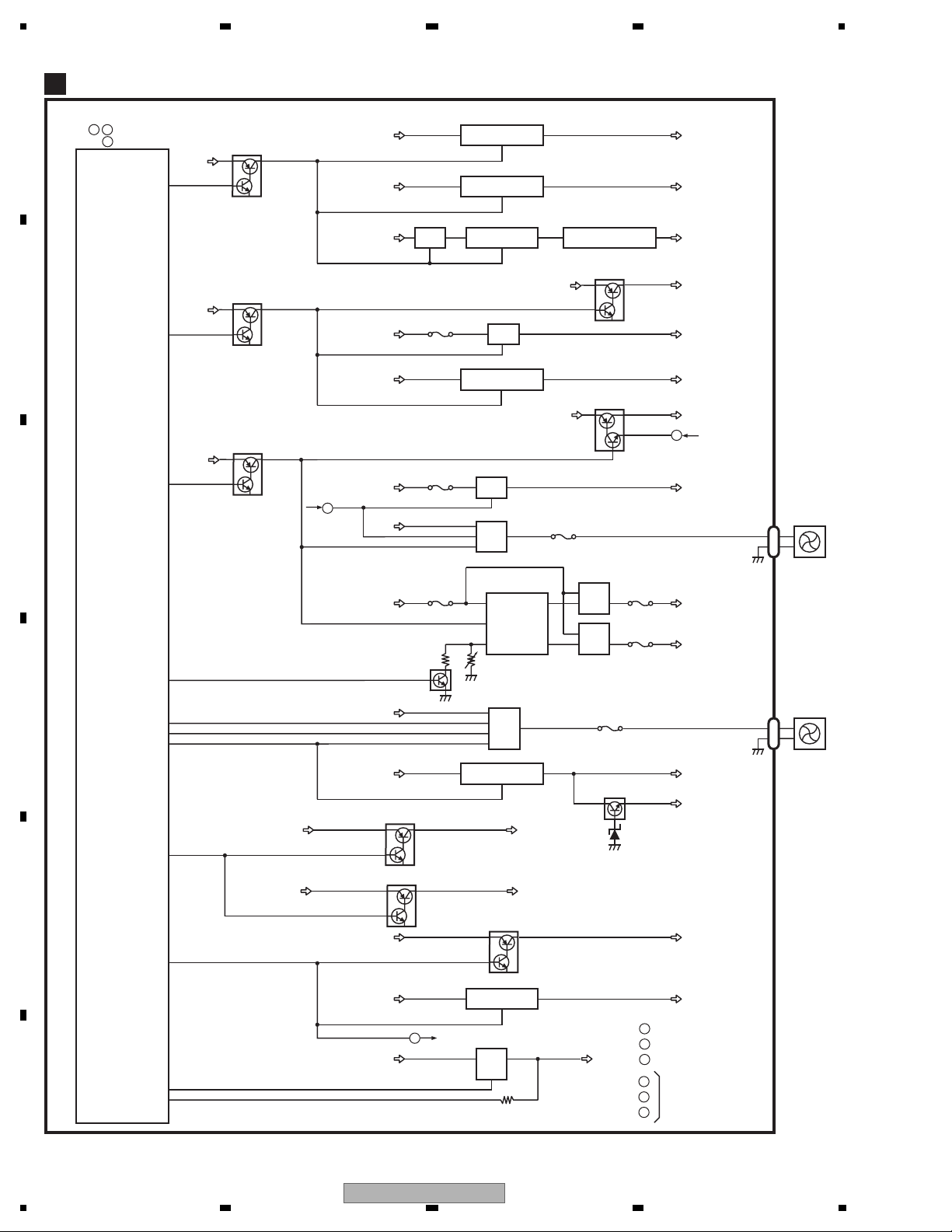
MOTHER UNIT (2/2)
A
SYSTEM MICON
A
B
C
IC601(2/2)
A
B
:PE5598A
C
:PE5597A
SYSPW
ACCPW
VDCONT
Q804
Q803
Q802
SYSPW1
ACCPW1
VDCONT1
to 1/2
E
VDD5
SYSPW
6
VDD5
ACCPW
7
VDD5
65
VDCONT
B.UP
B.UP
SYSPW1
B.UP
SYSPW1
B.UP PWVI
ACCPW1
B.UP
ACCPW1
B.UP PWFL
MFLPW
B.UP
VDCONT1
Q831
Q832
FU891
FU901
MFLPW
TUN+B
24
IC812
BA00DD0WHFP
1
SYS+B
24
IC821
BA00DD0WHFP
1
65
24
CAPTAIN7 HIOUT PW
IC832
LT3461AES6
4
PWVI
Q891
Q892
ILM+B
IC861
BA00DD0WHFP
1
PWFL
Q901
Q902
23
IC831
S-812C56AUA-C3K
ACC33V
VDD33
SWVDD5 OPT5
Q941
OPT5
Q931
CANTER FAN6V
Q961
Q963
|
FU961
HSEN
D
TUN+B
SYS+B
EV12V
ACC33V
ILM+B
to 1/2
CN961
2
1
CENTER
FAN
DDC FOR MS5AV code2
IC971
VR971
9
3
2
VCC
ON/OFF
RT
AN8011S
OUT1
OUT2
10
7
REAR FAN6V
Q951
|
Q954
VIDEO9V
24
IC801
BA00DD0WHFP
1
SENS33V
SWVDD5
Q853
SWVDD33
24
IC852
BA00CC0WFP
1
FIREWIRE PW
Q871
|
Q875
Q911
Q921
Q976
F
to 1/2
FU973
B.UP
VDCONT1
55
DDCCTL
D
COOLCNT1
COOLCNT2
VPW
56
57
118
B.UP
B.UP
VPW
SENS33V
VDD33
121
SENS5
SENS5V
VDD5 SENS5V
E
37
SWVDD
133 PPW
PPOWER
131
VDSENS
SENS5
VDD5 SWVDD5
VDD5
SWVDD
SWVDD
B.UP FWPW
F
Q972
Q974
Q973
Q975
FU951
VIDEO5V
Q801
FU972
FU971
VD8
VD5
VIDEO9
VIDEO5
SWVDD33
A
:AVH-P5900DVD/XNEW5
B
:AVH-P5900DVD/XN/RE
C
:AVH-P5900DVD/XN/UC
D
E
to 1/2
F
CN951
REAR
FAN
2
1
24
AVH-P5900DVD/XN/UC
1234
Page 25
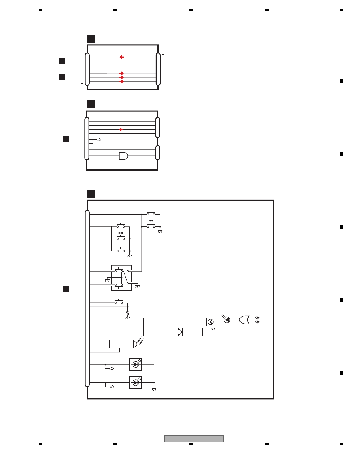
5 678
RCA PCB
G
A
A
CN391
CN311
A
CN461
CN4302
3
5
7
11
15
19
I
CN4201
18
15
13
12
7
6
5
4
VCRL
VCRV
VCAM
FL
RL
SWL
BUS+
BUS
BUSLI
ASENB
HSNS
OPTOUT
OPT PCB
-
DPT5
24
IC4201
TC7SET08FUS1
CN4301
VCRL
VCRV
BCAM
FL
RL
SWL
CN4202
BUS
BUS
BUSLI
ASENB
CN4203
4
6
8
12
16
20
+
1
-
4
6
7
3
2
VCR IN
RCA OUT
IP-BUS
DIGITAL OUT
A
B
A
CN481
KEYBOARD UNIT
B
CN4001
KEY0
7
SOURCE
ATT&VOLUME
1
3
2
S4031
RESET
REMOTE CONTROL
SENSOR
2
IC4021
SBX3050-01
ILMA
ILMB
8
2
4
11
15
10
12
14
6
9
3
5
KEY1
RDTA
RDTB
RESET
DSENS
LCDCL
LCDCE
LCDDI
REM
SWVDD5
ILMA
ILMB
S4035
S4036
S4037
BAND
S4032
4
5
SUB LCD CONTROL
47
46
48
1
D4051-D4060
D4071-D4080
S4033
EJECT
S4034
IC4001
LC75836WS
CLDIP1/S1
CE
1 SUBILM
SUB LCD
LCD4001
Q4041
D4042
ILMA
ILMB
C
D
E
56
AVH-P5900DVD/XN/UC
F
7
8
25
Page 26
1234
A
P
a
_
_
_
I
T
G
U
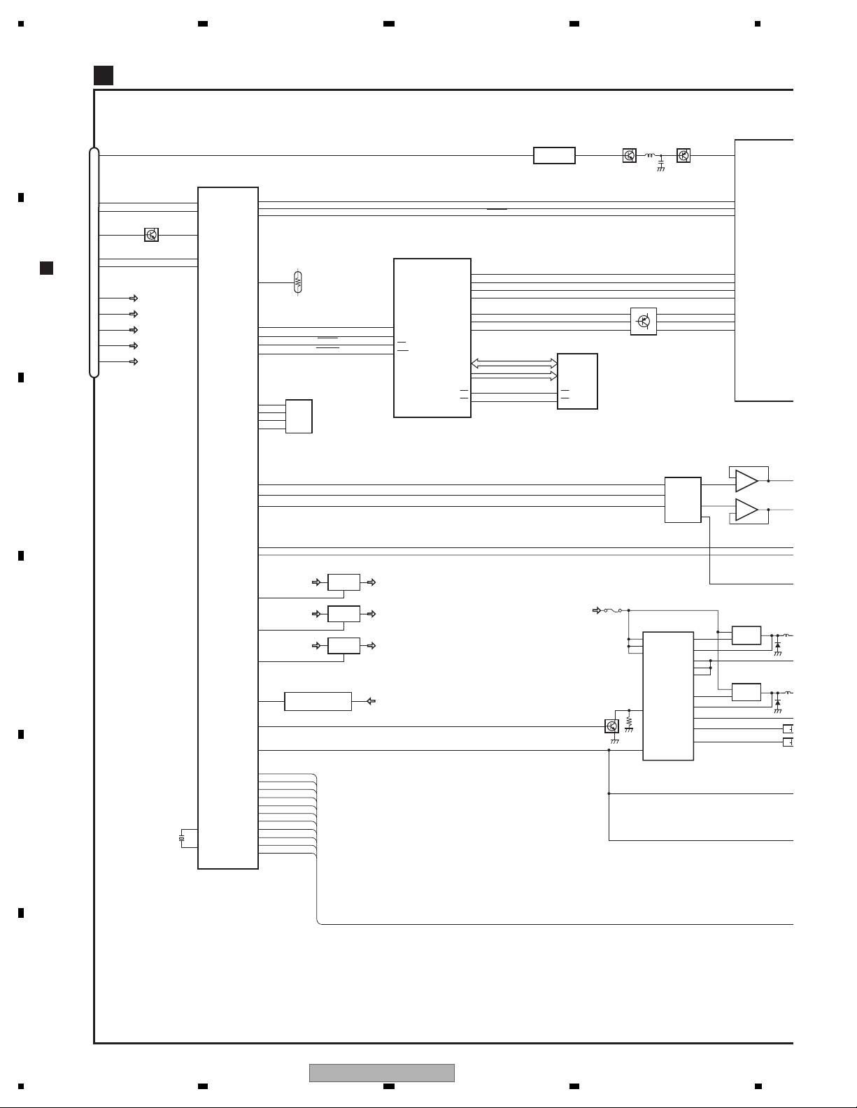
MONITOR PCB
C
A
PICTURE SPLI
IC5401
2
1
3
TC90A96BFGS
66
Sub_C.
Video_IN1
104
Bus_Clock_IN
105
Bus_Data_IN
107
Reset_IN
91
OSD_Clock_Out
92
OSD_V.Sync_Out
93
OSD_C/H.Sync_Out
101
OSD_Blank_High_IN
78
R_IN.2
79
G_IN.2
80
B_IN.2
2
+
3
5
+
6
-
1
IC5503
NJM2100V
7
R2-7
G2-7
B2-7
X
X'T
D
C.VIDEO
OSDCKL
OSDV
OSDH
BLK
Q5301
Q5801-Q5803
CN5003
C.VIDEO
30
REMCON
20
MFLPW
16
19
9
10
CN512
A
B
11
I
13
14
I
15
21
22
23
I
25
SWVDD
TXOSD
RXOSD
Q5601
PWRFL
PWRVI
ILMB
ILMA
SWVDD33V
MONITOR uCON
IC5603
PEG333A
5
REMIN
79
MFLPW
8
VDDSENS
34
DPDT
33
KYDT
PIPCK
PIPDA
PIPRST
TEMPSEN
100 OSDCK
OSDSCL
OSDDATA
OSDCS
OSDRES
EPRDI
EPRDO
EPRCK
EPRCS
27
28
25
TH5601
TEMP. SENSOR
87
99 OSDDA
19
20
S-93C56BD0I-J8
36
37
40
38
EEPROM
IC5604
4
DO
3
DI
2
SK
1
CS
OSDCS
OSDRST
PIPCK
PIPDA
PIPRES
OSD IC
IC5802
PDC149A
2
OSCin
9
VSYNC
11
HSYNC
30
BLK
34
ROUT
35
5
SCLK
6
SIN
7
CS
15
RST
GOUT
36
BOUT
58
57
OE OE
NJM2505AF
D0-11
A0-17
IC5301
26
28
14
OSD ROM
IC5801
PEH098A
CECE
C
DACDI
DACCLK
DACLD
3
4
2
DACDI
DACCLK
DACLD
IC5501
M62343FP
6
DILDA02
7
CLK
8
Q5302
OSDR
OSDG
OSDB
A01
A03
22
DIMMER
24
INVPUL
Q5602
ILMA DILMA
16
ILMR
17
ILMB
D
OSDPW
RESET
DDCON_SEL
MVIPW
PNLYV
PNLXY
TOUCHAD
PNLVD
PNLADX
PNLADY
XOUT
XIN
E
X5601
11
13
SWVDD33V OSD33V
18
1
10
S-80827CNNB-B8M
95 DDCON_SEL
80
78
PNLYV
88
PNLXV
93
TOUCHAD
89
PNLVD
91
uPNLADX
90
uPNLADY
68
KD1
67
KD2
66
KS1
65
KS2
92
LSEN
Q5603
Q5604
ILMB DILMB
Q5605
Q5607
Q5608
KDT1
KDT2
KST1
KST2
LSEN
RESET
IC5602
2
SWVDD33V
PWRVI
FU5101
Q5101
DIMMER
INVPUL
D/D CONVERTER
IC5103
BD6171KV
11
PVCC1
6
PVCC2
42
VCC
PVCC3
PVCC4
PVCC5
44
RT
32
EN1
OUT2
OVT1
OUT3
OUT4
OUT5
VS2
VS1
INVBST
7
4
23
48
37
3.3V REGULATOR
10
13
22
47
38
8V REGULATOR
Q5103
4
S
3
D
G
Q5102
4
S
D
3
G
1,2,5,6
1,2,5,6
CHAR
REG
F
26
1234
AVH-P5900DVD/XN/UC
Page 27
5 678
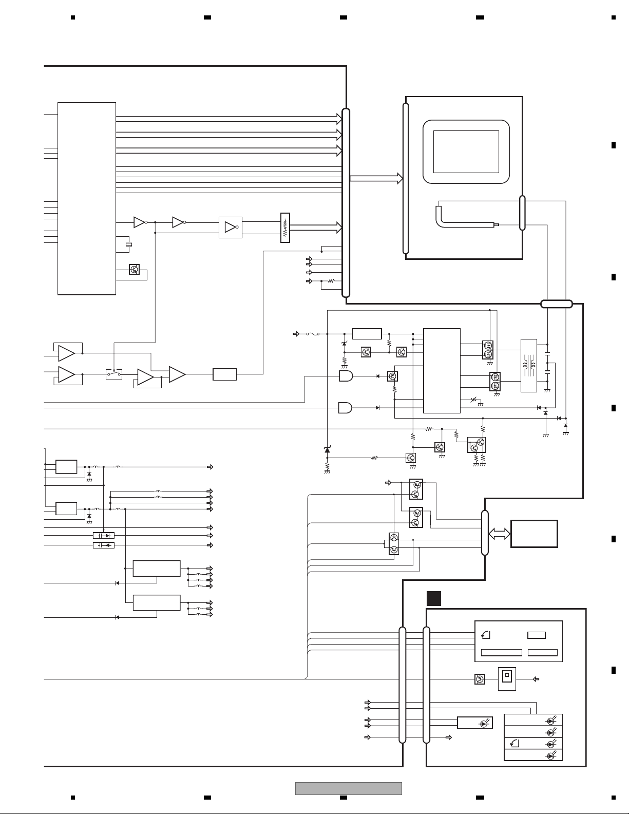
PICTURE SPLIT IC
TC90A96BFGSING
66
Sub_C.
Video_IN1
104
Bus_Clock_IN
105
Bus_Data_IN
107
Reset_IN
91
OSD_Clock_Out
92
OSD_V.Sync_Out
93
OSD_C/H.Sync_Out
101
OSD_Blank_High_IN
78
R_IN.2
79
G_IN.2
80
B_IN.2
2
+
3
NJM2100V
5
+
6
-
IC5401
1
IC5503
7
R2-7_D-Out
G2-7_D-Out
B2-7_D-Out
STH
Load
CPH
CPV
Vcom
X'Tal_IN
X'Tal_OUT
DAC_Out
PLL_IN
TC7S66FU
148-143
158-153
171--166
OE
134
STV
TC7SET04FUS1
133
52
53
60
56
VCOM AMP
4
IC5505
IC5502
X5401
42MHz
Q5401
521
6
+
-
TC7SET04FUS1
42
IC5507
NJM082BV
3
7
2
IC5504
2
+
-
4
1
DC0-5
DB0-5
DA0-5
DRIVER
IC5506
TC74VHC04FTS1
1,3,5
9,11,13
VCOM DRIVE
Q5501
Q5502
LADDER NETWORK
2,4,6
8,10,12
PWRFL
VCCM12V
VCC18V
VCC5V
VCC3.3V
VO0-10
FU5201
CN5501
30
|
35
36
|
41
42
|
47
STH1139
59
LOAD138
29
CPH137
20
OE136
9
CPV135
8
STV1
6
58
|
48
VCOM
1
VCOM
2
VGL
4
VGH
13
24
VDD2
I
26
L/R
28
16
VDD1
.
17
1
TC7SET08FUS1
IC5203
TC7SET08FUS1
1,2
5V REGULATOR
IC5201
TA78L05F
Q5202
4
IC5202
4
Q5204
Q5203
LCD MODULE
LCD
LCD BACK LIGHT
LCD DRIVE
IC5204
531
14
15
3
7
9
18
OZ961ISN
VDDA
DIM
LCT
ENA
V2500
FB
CT
PDRV_A
PDRV_B
PDRV_C
PDRV_D
OVP
RT
IC5205
SI6544DQ
19
20
12
11
VR5201
17
2
IC5206
SI6544DQ
4,5
2,3
CN5201
T5201
A
B
1
2
FL1
FL2
6
7
C
VBST
8V REGULATOR
Q5103
4
1,2,5,6
S
3
D
G
3.3V REGULATOR
Q5102
4
1,2,5,6
S
D
3
G
CHARGE PUMP
REGULATOR
2.5V REGULATOR
5
IC5102
S-1131B25UC-N4K
4
1.5V REGULATOR
5
IC5101
S-1131B15UC-N4A
4
INVBST
Q5703
2
7
8
9
11
5
6
4
3
10
Q5702
Q5701
Q5205
11
6
5
4
2
8
7
9
10
3
H
CN5901
KDT1
KDT2
KST1
KST2
LSEN
ILMA
ILMB
DILMA
DILMB
VCC8V
ILMA
ILMB
DILMA
DILMB
SWVDD33V
SWVDD33V
SWVDD33V
CN5002
KDT1
KDT2
KST1
KST2
LSEN
V33D
V33IO
V33
VCC3.3V
VCC5V
VCC18V
VCCM12V
1
1
V25
V25P
V25AM
V25AS
V15
V15M
V15D
PNLYV
PNLXV
TOUCHAD
PNLVD
uPNLADX
uPNLADY
Q5201
Q5206
CN5001
PLYV
1
PLXV
2
ADVX
3
ADVY
4
UPPER PCB
S5921 S5922
S5923 S5924
TI/PGM/XM_MEMO OPEN/CLOSE
Q5901
43
DISC
ON/OFF
SWD33
KEY MATRIX
D5901
TI/PGM/
XM_MEMO
DISP
OPEN/CLOSE
D
TOUCH
PA NE L
E
DISP
SWD33
F
56
AVH-P5900DVD/XN/UC
7
8
27
Page 28
1234
O
P
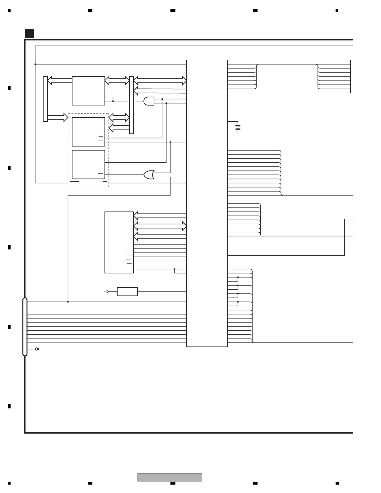
DVD CORE UNIT
D
A
B
C
D
NRES
LATCH
IC1352
TC74LCX16373FT
A0-15
A0-15
12
FLASH 16M
CWW1416
CWW1417
RESET
IC1401
IC1402
AD0-15
48
1LE
25
2LE
AD0-15
A16-19
XCSSR26
CE
WE
WE
XWR111
XCSFM26
CE
11 XWR2
XRDNRES 28 50
OE
SDRAM
IC1481
EDS1232AATA-75
IC1403
TC7SZ32FU
AD0-15
A16-19
1
4
2
IC1351
TC7SZ08FU
1
4
2
MA0-11
MDQ0-31
DQM0-3
22 8
BA0
23 10
BA1
WE
CAS
RAS
20
CS
68
CLK
VOLTAGE DETECT
IC1003
S-80859CNNB-B9K
2 1 VSENS
CN1951
PR_A20 92
11
EXTRG1_SPD_SW
10
SCLOCK
9
SDATA
8
EXTRG0
7
TRCCLK
6
TRCD0
5
TRCD1
4
TRCD2
DEBUG
3
TRCD3
2
TRCST
1
12
VCC33
|
13
VD8
OUTVDD
XWE17 3
XCAS18 4
XRAS19 5
XCSM 6
MCK 234
XCSSR
XCSFM
VIDEO+AUDIO
MN2DS0016AAUB
101
NRST
77
XCSSR
51
NEXCE
62
NEXWE
NEXOE
BA0
BA1
NWE
NCAS
NRAS
NCSM
MCK
232
MCKI
88
VSENCE
P0
189
EXTRG1
192
SCLOCK
191
SDATA
190
EXTRG0
188
TRCCLK
187
TRCDATA0
186
TRCDATA1
185
TRCDATA2
184
TRCDATA3
183
TRCST
IC1501
SRCK
ADOUT3
LRCK
SDODAC
SCKDAC
LTD AC
DACCK
OSCO
OSCI
Comp
STANDBY
SLVSTS
HOSTCMD
IRQPWR
AMUTE
DSCSNS
PHOTOSNS
IECOUT
CONT2
CONT1
DRV3
DRV2
LOADIN
CLAMP
HOME
TEMP
VIN2RF
VIN2
VIN1RF
VIN1
VIN3RF
VIN3
VIN4RF
VIN4
VIN5
VIN6
CDMPD
DVDMPD
RFINN
F+H_G+H
E+G_E+F
LPCO2
LPCO1
174
175
173
91
90
74
172 DACCLK
169
170
152
Cr
153
Cb
154
Y
161
78
79
80
89
87
147
144
179
85
84
95
96
97
MD
93
99
FG
150
FD
149
TD
94
98
145
122
142
123
143
121
140
120
141
136
137
130
128
116
134
135
131
129
X1501
(CR)
(CB)
(COMPOSIT)
LDIN
B
A
C
D
FE1
FE2
RF
(Y)
COMPOSIT
STANBY
STSCOMN
CMDCOMN
AUDI
SRCK
ADOUT3
LRCK
SDODAC
SCKDAC
LTD AC
DACCLK
1
2
3
13
14
15
16
CR
CB
Y
E
VDD5
F
28
1234
AVH-P5900DVD/XN/UC
Page 29
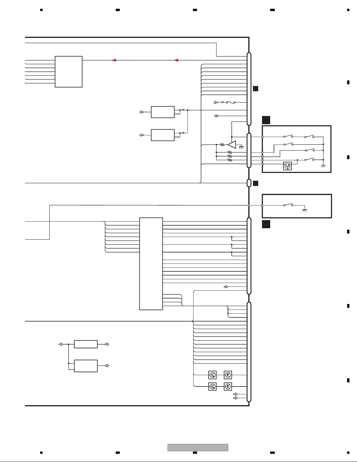
5 678
AUDIO 2CH ANALOG OUT
SRCK
ADOUT3
LRCK
SDODAC
SCKDAC
LTD AC
DACCLK
1
2
3
13
14
15
16
VDD5 VCC33
IC1801
PCM1753DBQ
VOUTL
BCK
DATA
LRCK
MD
MC
ML
SCK
NJM2885DL1-33
R1232D121B
2
VIN
3
7
3.3V REG.
IC1007
OUTIN
1.2V REG.
IC1008
VDD
A
B
VCC5
AVCC 5
VCC5 REG.
IC1004
NJM2880U1-05
4
VOUT
AVCC5 REG.
IC1005
S-L2980A50MC-C7J
5
VOUT
CONT
ON/OFF
5
VIN
1
1
VIN
3
LOUT
STSCOMN
CMDCOMN
VDD5
VD8
DISC DET
IC1301
TC7SZ125FU
CN1901
XRESETNRES
ANALOG LOUT
COMPOSIT
STANBY
SLVSTS
HSTCMD
IRQPWR
AMUTE
FU1901
WAKE UP
CN1301
DiscDetect
1
4DSCSNS 2
12cm
PhotoPHOTOSNS
VD5
VD8
8cm
8cm
21
29
CR
38
CB
36
Y
34
32
25
24
23
CN541
A
22
20
14
|
17
3
2
|
1
40
3
2
4
5
1
COMPOUND UNIT(A)
E
S1203
DISC SENS
4
3
2
5
6
8cm
12cm
8cm
S1202
Q1299
S1204
S1201
S1205
CN1852
IECOUT
1
CN462
A
C
CLAMP1
MOTOR DRIVER
IC1201
BD7996EFV
CONT2
CONT1
DRV3
DRV2
MD
FD
TD
31
8
LX
VCC12
20 18
CTL2 SLO2-
21
SLO1-
CTL1
25
SLIN2
SLO2+
26
SLIN1
SLO1+
29
SPIN
10
LDIN
13
FG
51
ACTIN1
50
ACTIN2
HW-
HW+
HV+
HU+
ACO1ACO1+
ACO2+
ACO2-
V
W
U
HB
HV-
HU-
16
17
15
42
39
44
36
30
31
32
33
34
35
2
FOM
1
FOP
TOM
3
TOP
4
COILV
COILW
COILU
HBM
HWM
HWP
HVM
HVP
HUM
HUP
LPCO2
LPCO1
VDD5
HALL_BIAS-
HALL_BIAS+
Q1104Q1102
Q1103Q1101
VREF
VCC5
CN1201
COIL_V
COIL_W
COIL_U
HALL_W-
HALL_W+
HALL_VHALL_V+
HALL_UHALL_U+
SWITCHHOME
CN1101
FOM
FOP
TOM
TOP
78MDCDMPD
65MDDVDMPD
F+H/G+HF+H_G+H
E+G/E+FE+G_E+F
LD(CD)
LD(DVD)
VCC
FE1
FE2
B-
AB+
A+
F-
F+
T-
T+
THTEMP
B
A
C
D
RF
1
2
3
4
5
6
7
8
9
10
11
12
13
14
15
16
17
18
20
1
2
3
4
5
7
8
9
10
11
12
14
15
PU (DP8)
17
21
22
24
25
19
20
TP1
F
S1206
CLAMP
COMPOUND UNIT(B)
D
E
56
AVH-P5900DVD/XN/UC
F
7
8
29
Page 30
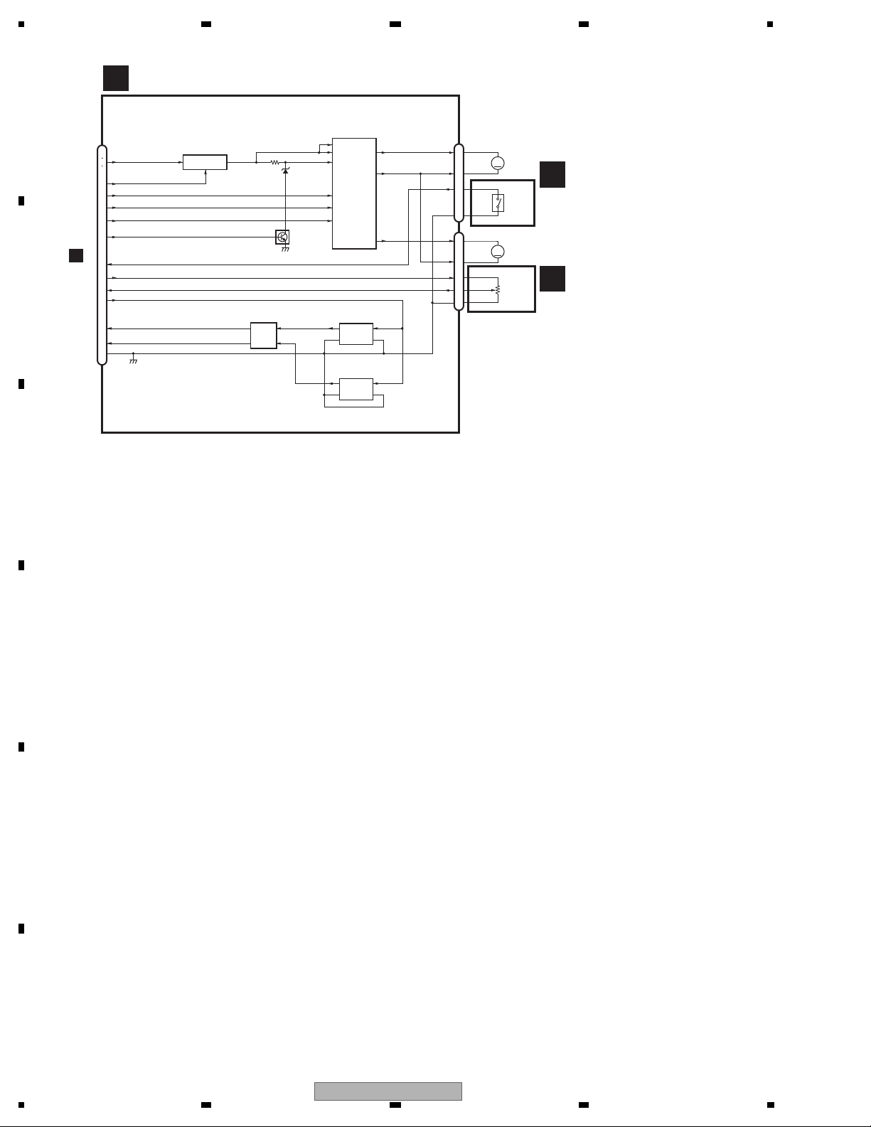
1234
J
MAIN PCB UNIT(SERVICE)
A
CN101
1
BUP
2
3
MTRPW
17
MTRSET
14
(ANG)MTR1
15
(POS)MTR2
16
MTRS
18
A
ANGLEOSW
13
CN512
B
10
20
11
19
12
8
3.3V
ANGLEIN
5V
LIFTPUL
LIFTSW
DGND
5V REGULATOR
2
IC101
BA00CC0WFP
1
4
WAVE SHAPE
TC7W14FU
7
5
IC104
1
1Y
1A
3
2Y
2A
MOTOR DRIVE
9
16
14
8
5
6
Q101
SLIDE PULSE OUTPUT
LIFT SW (EJECT:L)
BA6247FP
VCC1
VCC2
VR
IN3
IN1
IN2
GP2L24B
3
C
2
E
3
C
2
E
IC102
IC105
IC103
GP2L24B
OUT3
OUT1
OUT2
1
18
22
1
A
4
K
1
A
4
K
CN102
CN103
1
2
3
4
1
2
3
4
5
ANG_V
ANG_IN
ANG_G
SLIDE
M
MOTOR
S
G
M
K
S101
ANGLE
SWITCH
SWITCH PCB UNIT
ANGLE
MOTER
VR101
L
ANGLE
SENSER
VOLUME PCB UNIT
C
D
E
F
30
1234
AVH-P5900DVD/XN/UC
Page 31

5 678
A
B
C
D
E
56
AVH-P5900DVD/XN/UC
F
7
8
31
Page 32
1234
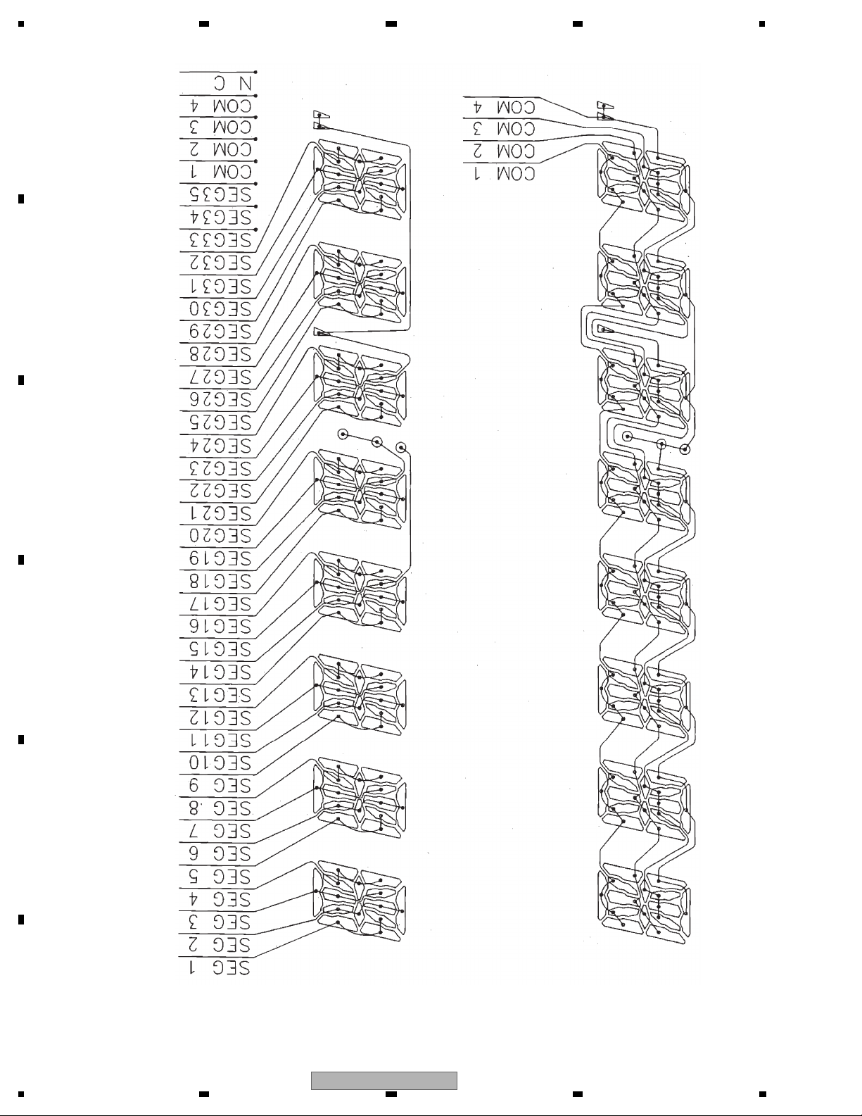
- CAW1946
A
B
C
D
E
SEGMENT
F
32
1234
AVH-P5900DVD/XN/UC
COMMON
Page 33
5 678
5. DIAGNOSIS
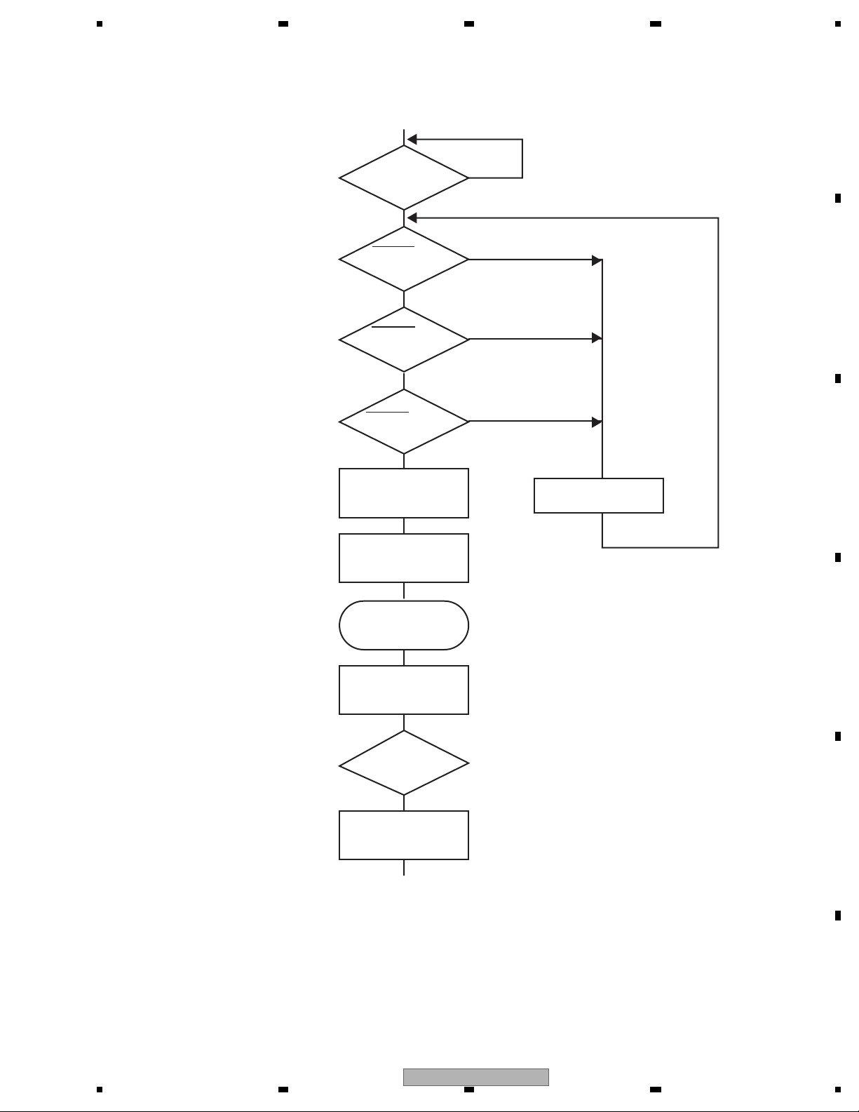
5.1 OPERATIONAL FLOW CHART
DSENS:
0 [v] to 0.85 [v] = OFF
0.85 [v] to 2.45 [v] = ON
2.45 [v] to 3.3 [v] = OFF
RESET
Vdd = 3.3V?
Pin 9
Y
BSENS=L?
Pin 21
Y
ASENS=L?
Pin 74
Y
DSENS=ON?
Pin 140
Y
ASENBO←H
Pin 30
A
B
C
Standby
SWVDD←H
Pin 37
Starts
communication
with Display
microcomputer.
Source keys
operative
Source ON
SYSPW←H
Pin 6
Completes power-on operation.
(After that, proceed to each source operation)
D
E
56
AVH-P5900DVD/XN/UC
F
7
8
33
Page 34
1234
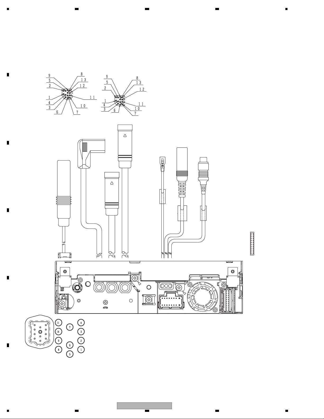
5.2 CONNECTOR FUNCTION DESCRIPTION
1.AVIN-
A
B
1.PWGND
2.PWPWR
3.TXiPod
4.ACCID
5.L
6.RXiPod
7.VIDEO
8.R
9.DGND
10.ACCPW
11.ACCDIT
ANTENNA CABLE
2.AVIN+
4.VSELIN1
5.VSELIN2
7.AVGND
10.REMIN
11.AVGND
BGSENS
1. MINIV
2. MINIVGND
3. MINIA
4. GND
5. MINIL
6. VGND
REAR MONITOR OUTPUT
C
12
D
1920
1. VCRRG
2. VCRR
3. VCRLG
4. VCRL
5. VCRVG
6. VCRV
1
2
E
1. FL-
1. BUS+
2. BUSG
3. LG
4. NC
5. BUS-
6. BUSG
7. BUSLI
8. ASENB
2. RL-
3. FL+
4. RL+
5. FR-
6. RR-
7. FR+
8. RR+
15
16
9. P.B.
10. VGND
11. ACC
12. B. REM
13. ILM
14. MUTE
15. B. UP
16. GND
9. BUSRI
F
10. BUSRG
11. BUSLG
7. BCAMG
8. BCAM
9. FRGND
10. FR
11. FLGND
12. FL
13. RRGEN
14. RR
15. RLGND
16. RL
17. SWRGND
18. SWR
19. SMLGND
20. SWL
34
AVH-P5900DVD/XN/UC
1234
Page 35
5 678
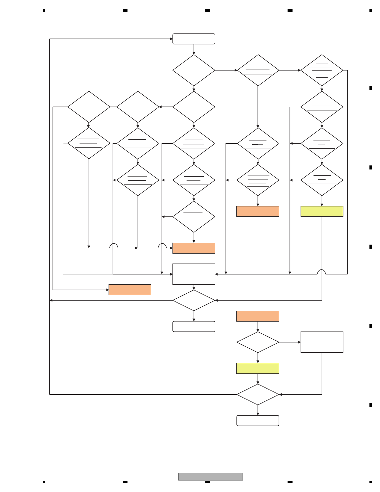
5.3 BACK END SECTION FLOW
START
Can the
playback
start?
YES
NO
Standby OK?
Execute check 1.
YES
NO
Is VDD5
(VCC33, VCC12)
power supply
voltage OK?
Execute
check 2.
YES
A
NO
NO
Does the
operation
take time?
Is the life of flash
memory OK?
Conduct check item 12.
NO
YES
YES
NO
Is the image
in error?
Is AVCC5
NO
voltage OK?
Execute check 8.
Is the video
NO
circuit OK?
Execute check 11.
Go to FE
section check.
YES
YES
YES
NO
NO
NO
NO
NO
Is the sound
in error?
YES
Is AVCC5
voltage OK?
Execute check 8.
YES
Is DACCLK
normal?
Execute check 9.
YES
Is the audio
circuit OK?
Execute check 10.
YES
Go to FE
section check.
Repair the
defective part.
Normal?
NO
NO
section check.
Is SDRAM
IF OK?
Execute check 6.
YES
Is VD8, VCC5
power supply
voltage OK?
Execute check 7.
YES
Go to FE
NO
Reset OK?
Execute check 3.
NO
Execute check 4.
NO
Execute check 5.
Replace the unit.
YES
Is VSENS
OK?
YES
Is 27 MHz
OK?
YES
B
C
D
YES
END
NO
AVH-P5900DVD/XN/UC
56
FE section check.
Is FE section
normal?
YES
Replace the unit.
Normal?
YES
END
7
NO
Go to FE related
repair process.
8
E
F
35
Page 36
1234
DGND1
STANBY
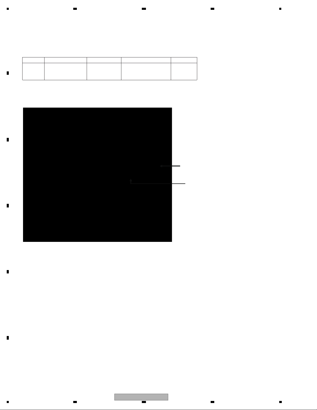
Check 1: Standby OK?
A
<Check> Check the voltage at the “STANBY” test point while the power is on.
Use the “DGND1” test point at the reference.
NO. Check point Module No.
STANBY-DGND1 ALL
1
Specification value
VCC33 V-
Unit
V
0.6 V or more
B
C
Side A
D
Fig 1.1: STANBY check point
E
F
36
AVH-P5900DVD/XN/UC
1234
Page 37
5 678
DGND1
VCC 12_1
VCC 33
VDD 5_3
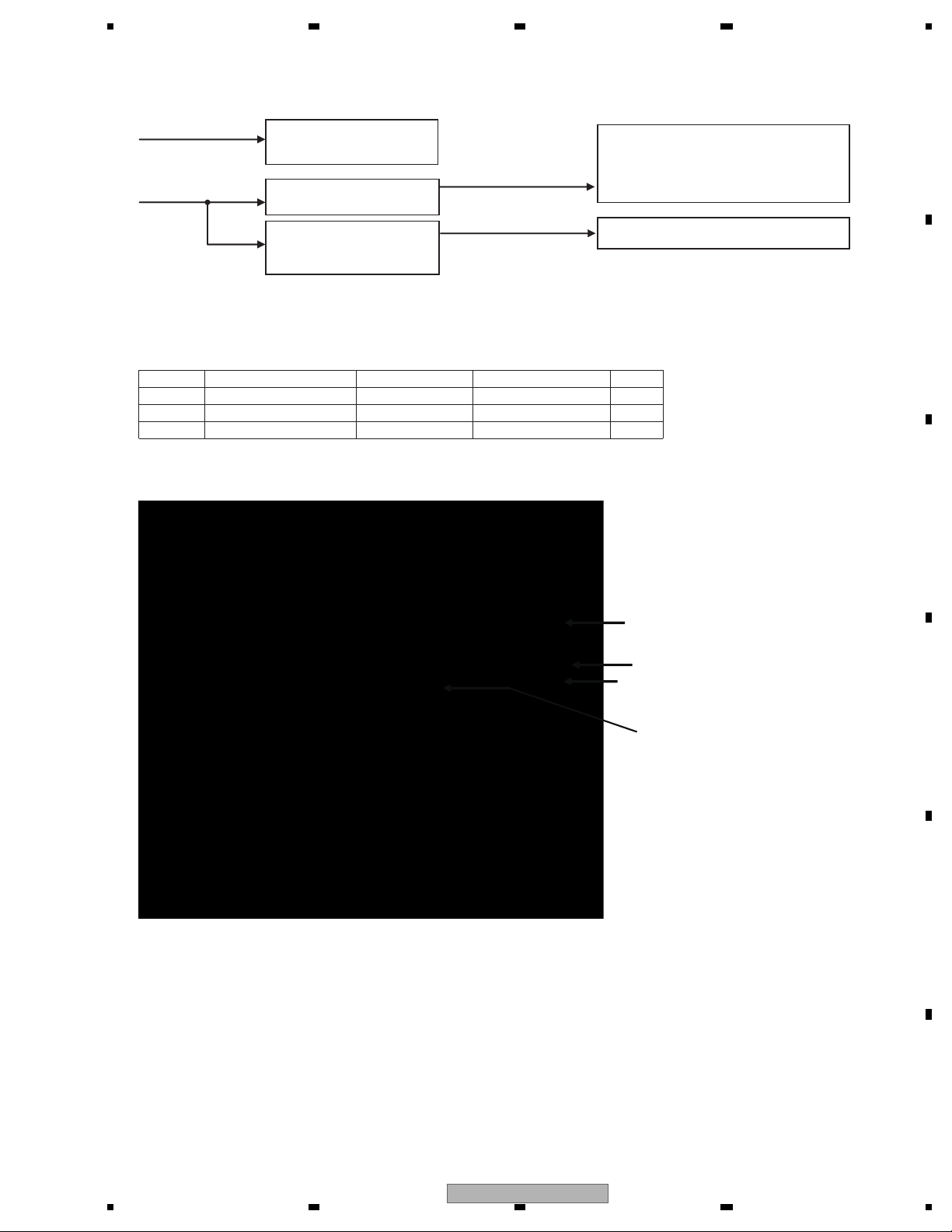
Check 2: Is VDD5 (VCC33, VCC12) power supply voltage OK?
VDD5
F.E. driver control system
IC1401 FLASH power supply (Data)
IC1402 FLASH power supply (Program)
IC1481 SDRAM power supply
VDD5
IC1007
3.3 V output regulator
IC1008
VCC33 (= 3.3 V )
VCC12 (= 1.2 V )
IC1501 DVD-LSI power supply
IC1501 DVD-LSI power supply
DC/DC converter
1.2 V output
Fig 2.1: Power supply configuration
<Check> Check the voltage at the “VDD5_3, VCC33_3 and VCC12_1” test point while the power is on.
Use the “DGND1” test point at the reference.
NO. Check point Module No.
1
VDD5_3 - DGND1
2
VCC33_3 - DGND1
3
VCC12_1 - DGND1
ALL
ALL
ALL
Specification value
5.0 ± 0.4
3.3 ± 0.15
1.2 ± 0.12
Unit
V
V
V
Side A
A
B
C
Fig 2.2: VDD5, VCC33, VCC12 voltage check points
D
E
F
56
AVH-P5900DVD/XN/UC
7
8
37
Page 38
1234
DGND1
XRES
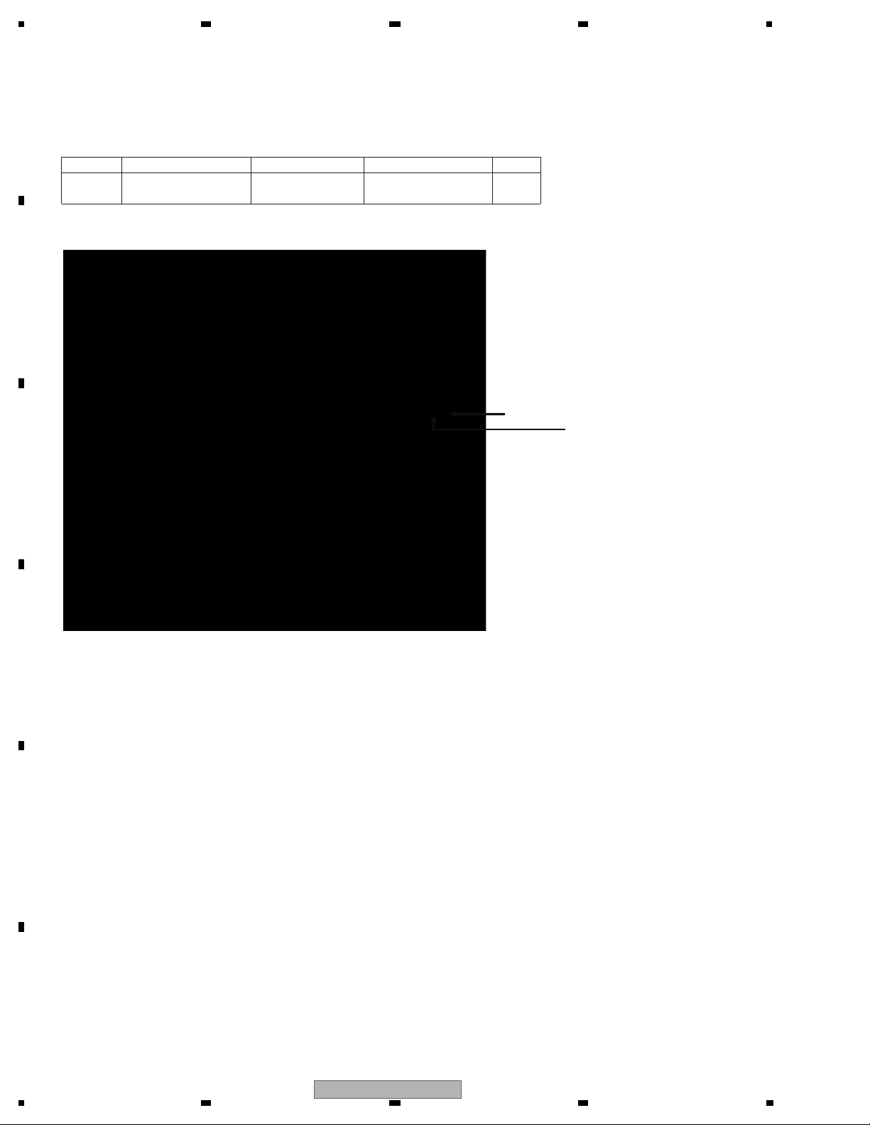
Check 3: Reset OK?
A
<Check> Check the voltage at the “XRES” test point while the power is on.
Use the “DGND1” test point at the reference.
NO. Check point Module No. Specification value Unit
1 XRES-DGND1 ALL
VCC33 ×
V
0.7 or more
Side A
B
C
D
E
F
Fig 3.1: RESET check point
38
AVH-P5900DVD/XN/UC
1234
Page 39
5 678
DGND1
VSENS
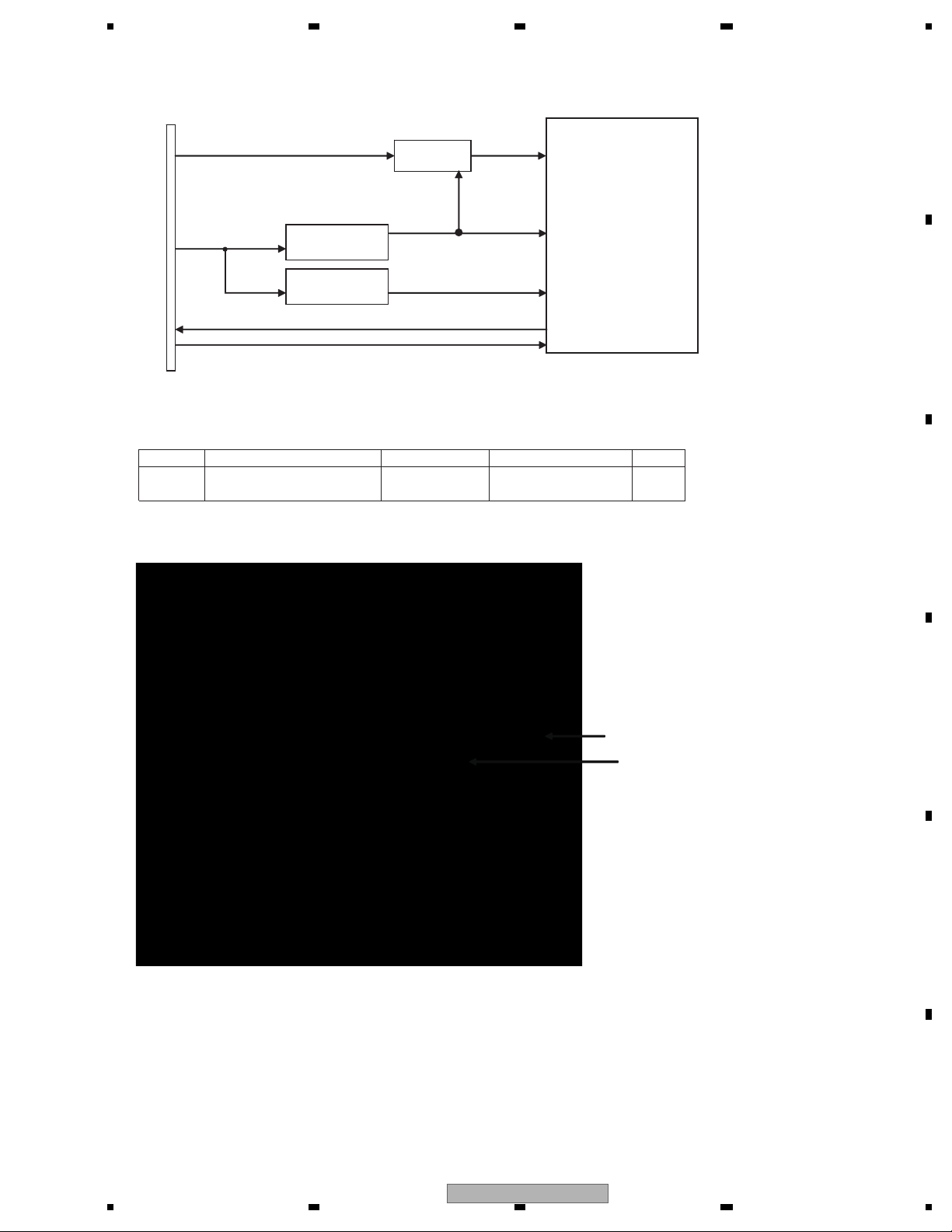
Check 4: Is VSENS OK?
CN1901
HOST I/F
VD8 VSENS
IC1003
detection IC
IC1501
A
DVD-LSI
VDD5
IC1007
Regulator
IC1008
DC/DC converter
VCC33
VCC12
STANBY
XRES
Fig 4.1: Power supply configuration and VSENS
<Check> Check the voltage at the “VSENS” test point while the power is on.
Use the “DGND1” test point at the reference.
NO. Check point
VSENS - DGND1 ALL
Module No.
Specification value
VCC33 × 0.7
or more
Side A
B
Unit
V1
C
Fig 4.2: VSENS check point
D
E
F
56
AVH-P5900DVD/XN/UC
7
8
39
Page 40
1234
DGND1
IC1501 169pin
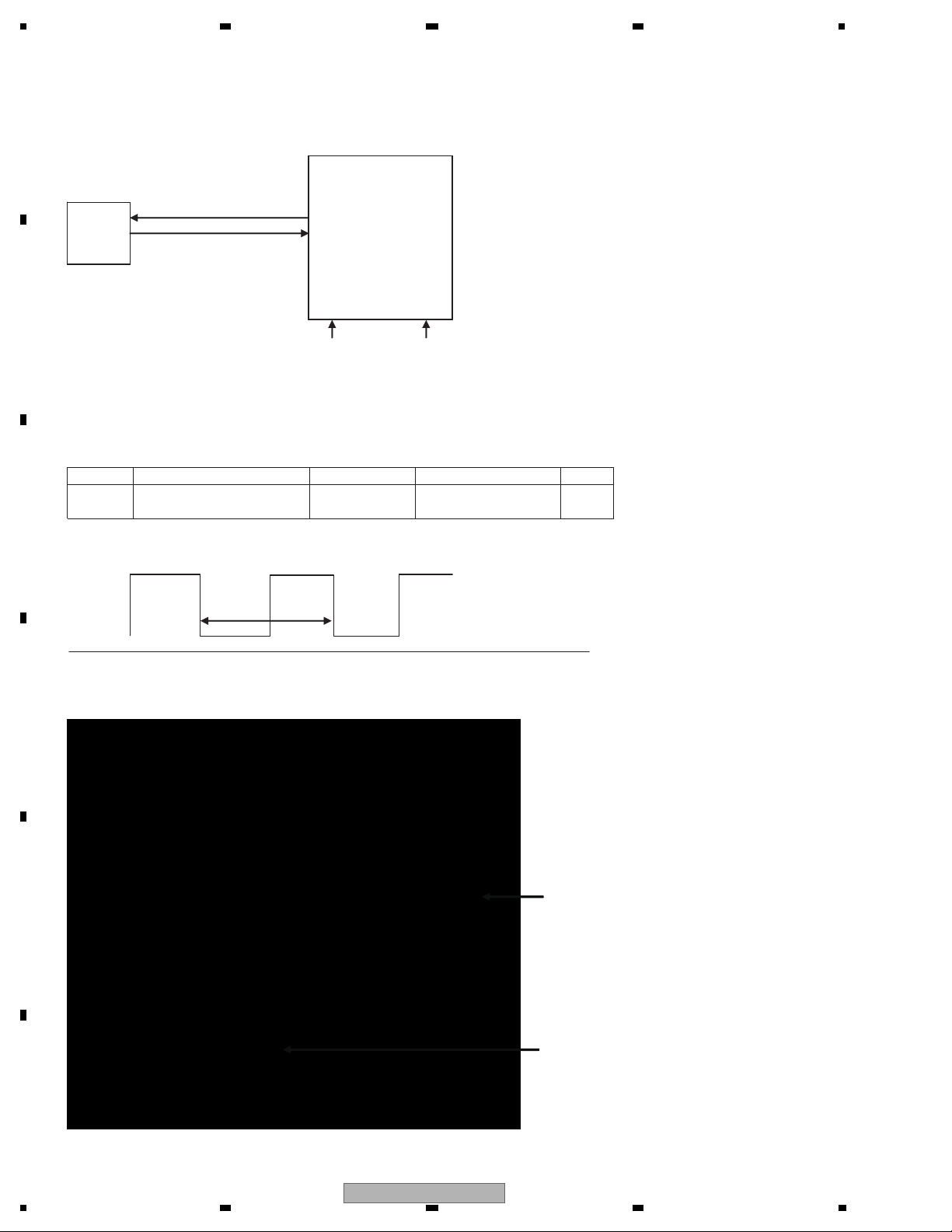
Check 5: 27 MHz Normal?
<Outline> Each clock is created inside the IC1501 using the 27 MHz master crystal oscillator (X1501).
A
IC1501
X1501
OSCO
27 MHz
DVD-LSI
crystal
B
OSCI
VCC33 VCC12
Fig 5.1: Clock configuration
<Check method> Turn the power on, and check with DGND being the reference.
In case of NG, check the applicable line, periphery of IC1501,
soldering of the peripheral components and defective components.
NO. Check point Module No.
2 IC1501 169pin ALL
C
Specification
value
Specification value
27 MHz
± 50 ppm
Unit
ppm
GND
Fig 5.2: Clock specification value
Side A
D
E
F
40
Fig 5.3: 27 MHz check point
AVH-P5900DVD/XN/UC
1234
Page 41
5 678
Check 6: Is SDRAM I/F OK?
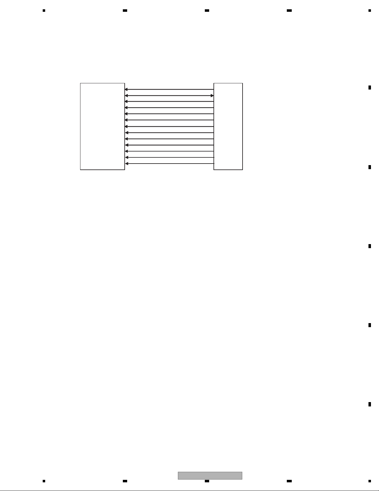
<Outline> In order to secure the MPEG stream data as the buffer,
the capacity of communication I/F SDRAM between the LSI and the memory is 128Mbit.
Be careful as XCSM, XWE, XCAS, XRAS and XSCM of IC1481 are called differently in IC1501,
namely NCSM, NWE, NCAS, NRAS, NCSM.
IC
1481
SDRAM
MA0~11
MDQ0~31
MCK
XWE (NWE)
XCAS (NCAS)
XRAS (NRAS)
XCSM (NCSM)
DQM0
DQM1
DQM2
DQM3
BA0
BA1
IC1501
DVD-LSI
Fig 6.1: SDRAM I/F
A
B
C
D
E
F
56
AVH-P5900DVD/XN/UC
7
8
41
Page 42
1234
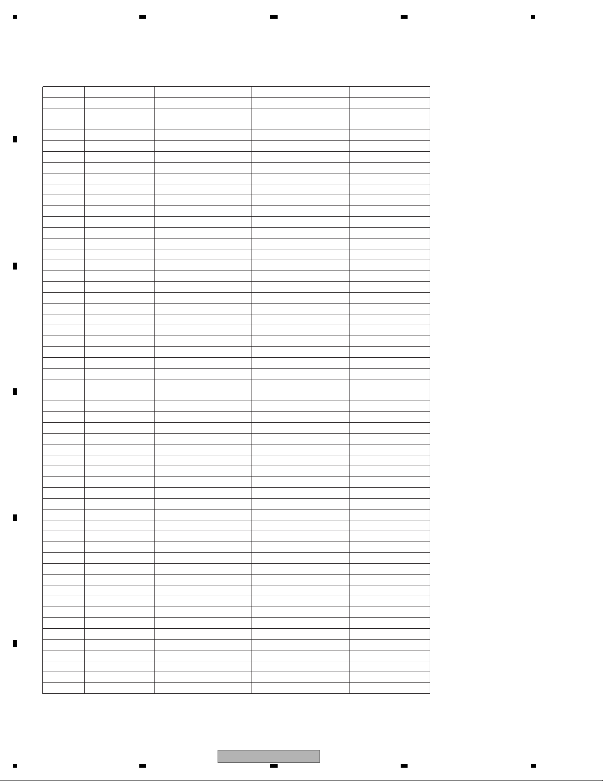
<Check> Check the conductivity at “check point 1” and “check point 2” without power.
In case of NG, check the soldering and defective components throughout the
“output t input” of the applicable section.
A
NO. Signal name Check point 1 Check point 2 Specification value
1
MA0
2
MA1
3
MA2
4
MA3
5
MA4
6
MA5
7
MA6
8
MA7
9
MA8
10
11
12
13
14
15
16
17
18
19
20
21
22
23
24
25
26
27
28
29
30
31
32
33
34
35
36
37
38
39
40
41
42
43
44
45
46
47
48
49
50
51
52
53
54
55
MA9
MA10
MA11
MDQ0
MDQ1
MDQ2
MDQ3
MDQ4
MDQ5
MDQ6
MDQ7
MDQ8
MDQ9
MDQ10
MDQ11
MDQ12
MDQ13
MDQ14
MDQ15
MDQ16
MDQ17
MDQ18
MDQ19
MDQ20
MDQ21
MDQ22
MDQ23
MDQ24
MDQ25
MDQ26
MDQ27
MDQ28
MDQ29
MDQ30
MDQ31
MCK
XWE
XCAS
XRAS
XCSM
DQM0
DQM1
DQM2
DQM3
BA0
BA1
B
C
D
E
IC1481 25pin
IC1481 26pin
IC1481 27pin
IC1481 60pin
IC1481 61pin
IC1481 62pin
IC1481 63pin
IC1481 64pin
IC1481 65pin
IC1481 66pin
IC1481 24pin
IC1481 21pin
IC1481 2pin
IC1481 4pin
IC1481 5pin
IC1481 7pin
IC1481 8pin
IC1481 10pin
IC1481 11pin
IC1481 13pin
IC1481 74pin
IC1481 76pin
IC1481 77pin
IC1481 79pin
IC1481 80pin
IC1481 82pin
IC1481 83pin
IC1481 85pin
IC1481 31pin
IC1481 33pin
IC1481 34pin
IC1481 36pin
IC1481 37pin
IC1481 39pin
IC1481 40pin
IC1481 42pin
IC1481 45pin
IC1481 47pin
IC1481 48pin
IC1481 50pin
IC1481 51pin
IC1481 53pin
IC1481 54pin
IC1481 56pin
IC1481 68pin
IC1481 17pin
IC1481 18pin
IC1481 19pin
IC1481 20pin
IC1481 16pin
IC1481 71pin
IC1481 28pin
IC1481 59pin
IC1481 22pin
IC1481 23pin
IC1501 16pin
IC1501 18pin
IC1501 20pin
IC1501 22pin
IC1501 21pin
IC1501 19pin
IC1501 17pin
IC1501 15pin
IC1501 11pin
IC1501 9pin
IC1501 14pin
IC1501 7pin
IC1501 237pin
IC1501 239pin
IC1501 241pin
IC1501 243pin
IC1501 248pin
IC1501 250pin
IC1501 252pin
IC1501 254pin
IC1501 253pin
IC1501 251pin
IC1501 249pin
IC1501 244pin
IC1501 242pin
IC1501 240pin
IC1501 238pin
IC1501 236pin
IC1501 29pin
IC1501 31pin
IC1501 33pin
IC1501 37pin
IC1501 39pin
IC1501 41pin
IC1501 43pin
IC1501 45pin
IC1501 44pin
IC1501 42pin
IC1501 40pin
IC1501 38pin
IC1501 34pin
IC1501 32pin
IC1501 30pin
IC1501 28pin
IC1501 234pin
IC1501 3pin
IC1501 4pin
IC1501 5pin
IC1501 6pin
IC1501 255pin
IC1501 256pin
IC1501 26pin
IC1501 27pin
IC1501 8pin
IC1501 10pin
Ω ± 5 %
56
Ω ± 5 %
56
Ω ± 5 %
56
Ω ± 5 %
56
Ω ± 5 %
56
Ω ± 5 %
56
Ω ± 5 %
56
Ω ± 5 %
56
Ω ± 5 %
56
Ω ± 5 %
56
Ω ± 5 %
56
Ω ± 5 %
56
Ω ± 5 %
56
Ω ± 5 %
56
Ω ± 5 %
56
Ω ± 5 %
56
Ω ± 5 %
56
Ω ± 5 %
56
Ω ± 5 %
56
Ω ± 5 %
56
Ω ± 5 %
56
Ω ± 5 %
56
Ω ± 5 %
56
Ω ± 5 %
56
Ω ± 5 %
56
Ω ± 5 %
56
Ω ± 5 %
56
Ω ± 5 %
56
Ω ± 5 %
56
Ω ± 5 %
56
Ω ± 5 %
56
Ω ± 5 %
56
Ω ± 5 %
56
Ω ± 5 %
56
Ω ± 5 %
56
Ω ± 5 %
56
Ω ± 5 %
56
Ω ± 5 %
56
Ω ± 5 %
56
Ω ± 5 %
56
Ω ± 5 %
56
Ω ± 5 %
56
Ω ± 5 %
56
Ω ± 5 %
56
Ω ± or lower
0.17
Ω ± 5 %
56
Ω ± 5 %
56
Ω ± 5 %
56
Ω ± 5 %
56
Ω ± 5 %
56
Ω ± 5 %
56
Ω ± 5 %
56
Ω ± 5 %
56
Ω ± 5 %
56
Ω ± 5 %
56
F
42
1234
AVH-P5900DVD/XN/UC
Page 43

Side B
5 678
A
B
Side A
Check point 1 (IC1481)
C
D
E
Check point 2 (IC1501)
Fig 6.2: SDRAM I/F check point
AVH-P5900DVD/XN/UC
56
F
7
8
43
Page 44
1234
VCC5_1
AGND1
VD
VD8_1
PGND3
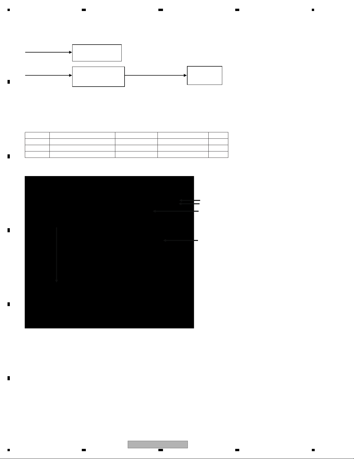
Check 7: Is VD8, VCC5 power supply voltage OK?
A
VD8_1
F.E. driver system
DISC detection LED
VD VCC5 (= 5.0V )
IC1004
REG IC
Power supply
for PU
for VCC 5V.
Fig 7.1: Power supply configuration
B
<Check> Check the voltage at the “VD8_1, VD and VCC5_1” test point while the power is on.
Use the “PGND3 and AGND1” test point at the reference.
NO. Check point Module No. Specification value Unit
1
VD8_1 - PGND3
2
VD - PGND3
3
VCC5_1- AGND1
ALL
ALL
ALL
8.0 ± 0.4
8.0 ± 0.4
5.0 ± 0.1
V
V
V
Side A
C
D
Fig 7.2: VD8, VCC5 voltage check points
E
F
44
AVH-P5900DVD/XN/UC
1234
Page 45
5 678
PGND3
AVC C5
GNDAU
VD
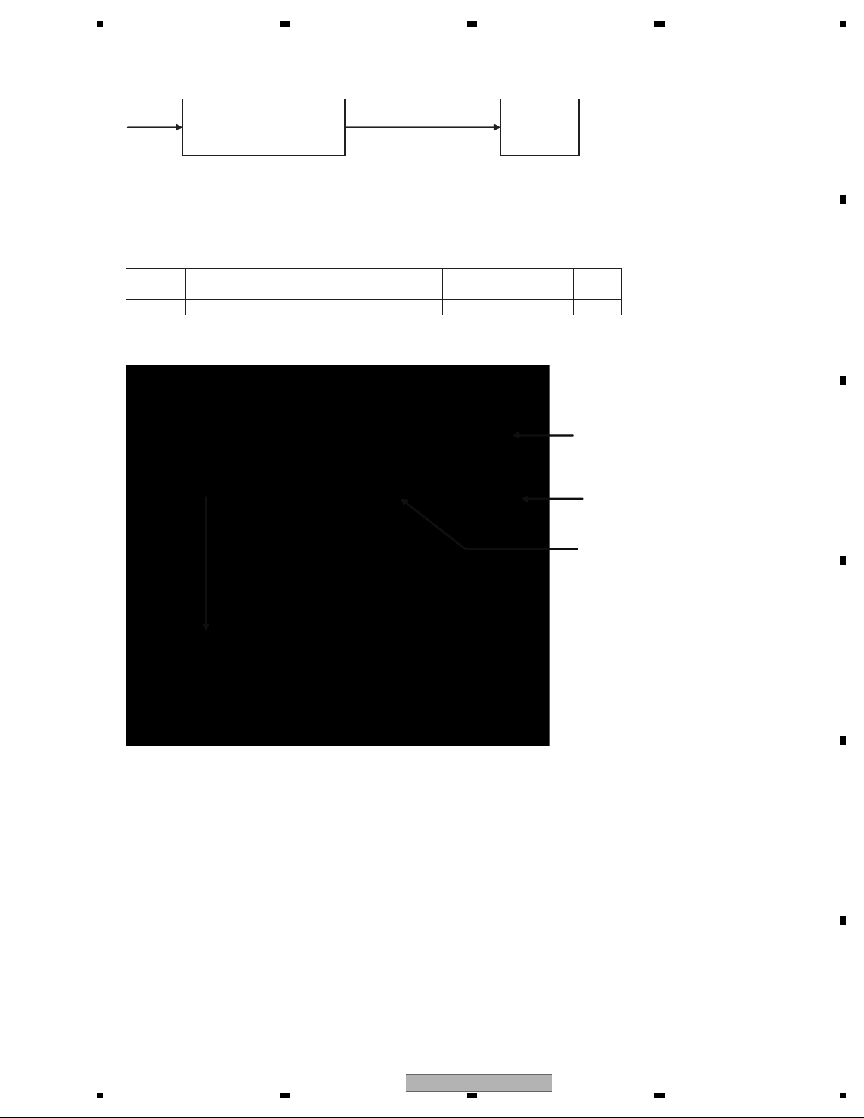
Check 8: Is AVCC5 voltage OK?
VD AVCC5 (= 5.0 V )
IC1005
REG IC
for AVCC 5 V.
IC1801
Audio-DAC
Fig 8.1: Power supply configuration
<Check> Playback DVD-REF-A1 TITLE 1 and check the voltage at the stylus.
Check with PGND and GNDAU being the reference.
NO. Check point
VD - PGND_3
1
AVCC5 - GNDAU1
2
Module No. Specification value Unit
ALL
ALL
8.0 ± 0.4
5.0 ± 0.1
Side A
A
V
B
V
C
Fig 8.2: VD8, AVCC5 voltage check points
D
E
F
56
AVH-P5900DVD/XN/UC
7
8
45
Page 46
1234
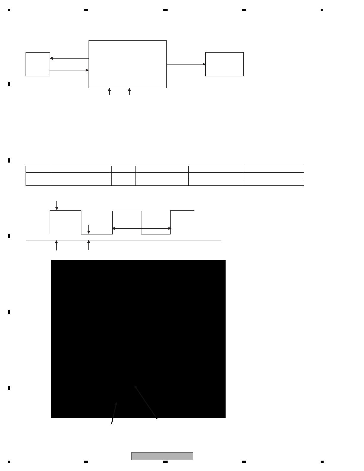
Check 9: Is DACCLK normal?
<Outline> DACCLK for Audio-DAC is created by IC1501 using the 27 MHz master crystal oscillator (X1501).
A
27 MHz
crystal
IC1501
DVD-LSIX1501
VCC33 VCC12
Fig 9.1: Clock configuration
DACCLK
IC1801
Audio-DAC
B
<Check method>
DVD: DVD-REF-A1 TITLE 1
CD: Playback a normal CDDA.
Common to all DVD-V compatible modules.
Check with DGND being the reference.
In case of NG, check the applicable line, the periphery of IC1501, soldering of the peripheral components and
defective components.
NO.
Check point 1 (stylus)
12DACCK
DACCK
Media Specification value 1 Specification value 2 Specification value 3
DVDCD2.0 V~VCC33 V
2.0 V~VCC33 V
DGND~0.8 V
DGND~0.8 V
36.8640 MHz±300 ppm
33.8688 MHz±300 ppm
Specification
C
value 1
Specification
value 2
Specification
value 3
GND
Fig 9.2: Clock specification value
Side A
D
E
F
Check point 1 (stylus)
Check point 2 (IC1501 172 pin)
Fig 9.3: 27 MHz, DACCLK check point
46
1234
AVH-P5900DVD/XN/UC
Page 47
5 678
SRCK
LRCK
ADOUT3
Check 10: Is the audio circuit OK?
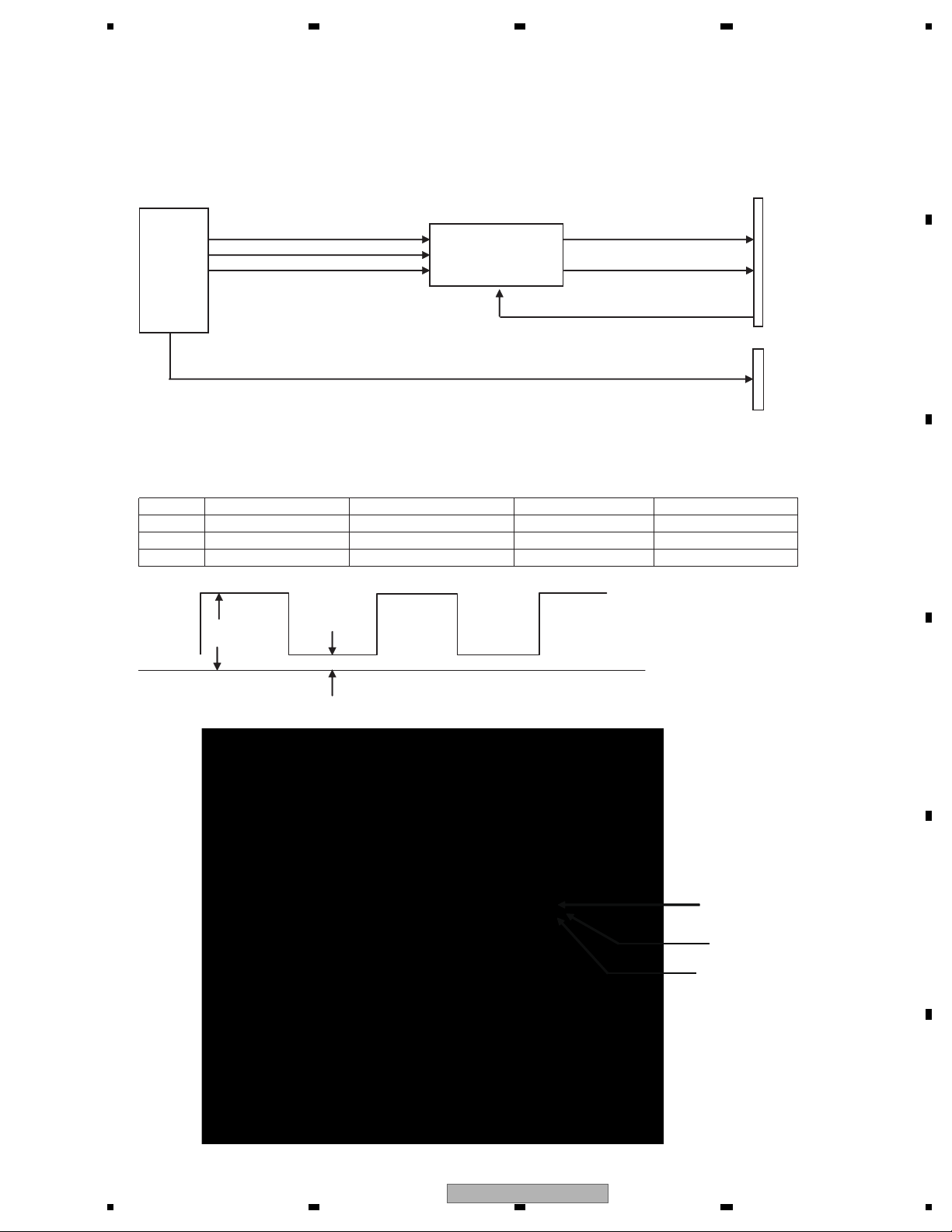
<Outline> The serial 3 lines digital output + DACCLK, output from DVD-LSI (IC1501), are converted to analog audio
signal at Audio-DAC (IC1801) and are output from the HOST I/F (CN1901).
Simultaneously, the analog MUTE signal is also output from DVD-LSI (IC1501) via the HOST I/F.
The digital audio signal (IECOUT), output from DVD-LSI (IC1501), is output via CN1852.
CN1901
HOST I/F
IC1501
DVD-LSI
LRCK LO
ADOUT3
SRCK RO
IC1801
Audio-DAC
A
GNDAU
CN1852
IEC
Fig 10.1: Audio circuit
<Check method> Playback DVD-REF-A1 TITLE 2 CHAPTER 1 (48 k/16 bit 1 kHz 0 dB),
and check with DGND being the reference.
In case of NG, check the applicable line, periphery of major components as described in the above drawing,
soldering of the peripheral components and defective components.
NO. Check point 1 (stylus)
1
ADOUT3
2
SRCK
3
LRCK
Specification value 1
VCC33 V-0.6 V or higher
VCC33 V-0.6 V or higher
VCC33 V-0.6 V or higher
Specification value 2
0.4 V or lower
0.4 V or lower
0.4 V or lower
Reference waveform
Waveform 1
Waveform 2
Waveform 3
Specification
Specification
value 2
value 1
GND
Fig 10.2: Serial 3 lines specification value
Side A
B
C
D
Fig 10.3: Serial 3 lines check points
AVH-P5900DVD/XN/UC
56
E
F
7
8
47
Page 48
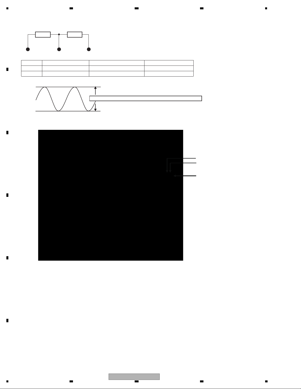
1234
LO
RO
GNDAU1
The following checks shall be conducted using the following measurement circuits with GNDAU1 being the reference.
47 kΩ 47 kΩ
A
LO GNDAU1 RO
NO.
Check point 1 (stylus)
4
LO
5
RO
Specification value (rms)
1 400 ± 150 mV
1 400 ± 150 mV
Reference waveform
Waveform 4
Waveform 4
B
Specification value is the root-mean-square value (rms).
Fig 10.4: Analog audio out (LO, RO) specification value.
Side A
C
D
E
F
48
Fig 10.5: Analog audio out check point
AVH-P5900DVD/XN/UC
1234
Page 49

5 678
IEC
Check with DGND being the reference.
Check 2pin cord after connecting it to a jig, etc.
NO. Check point 1 (stylus) Specification value 1
6 IEC VCC33 V-0.6 V or higher 0.4 V or lower Waveform 5
Side A
Specification value 2
Reference waveform
A
B
Fig 10.6: Digital audio signal (IECOUT) check point
C
D
E
56
AVH-P5900DVD/XN/UC
F
7
8
49
Page 50
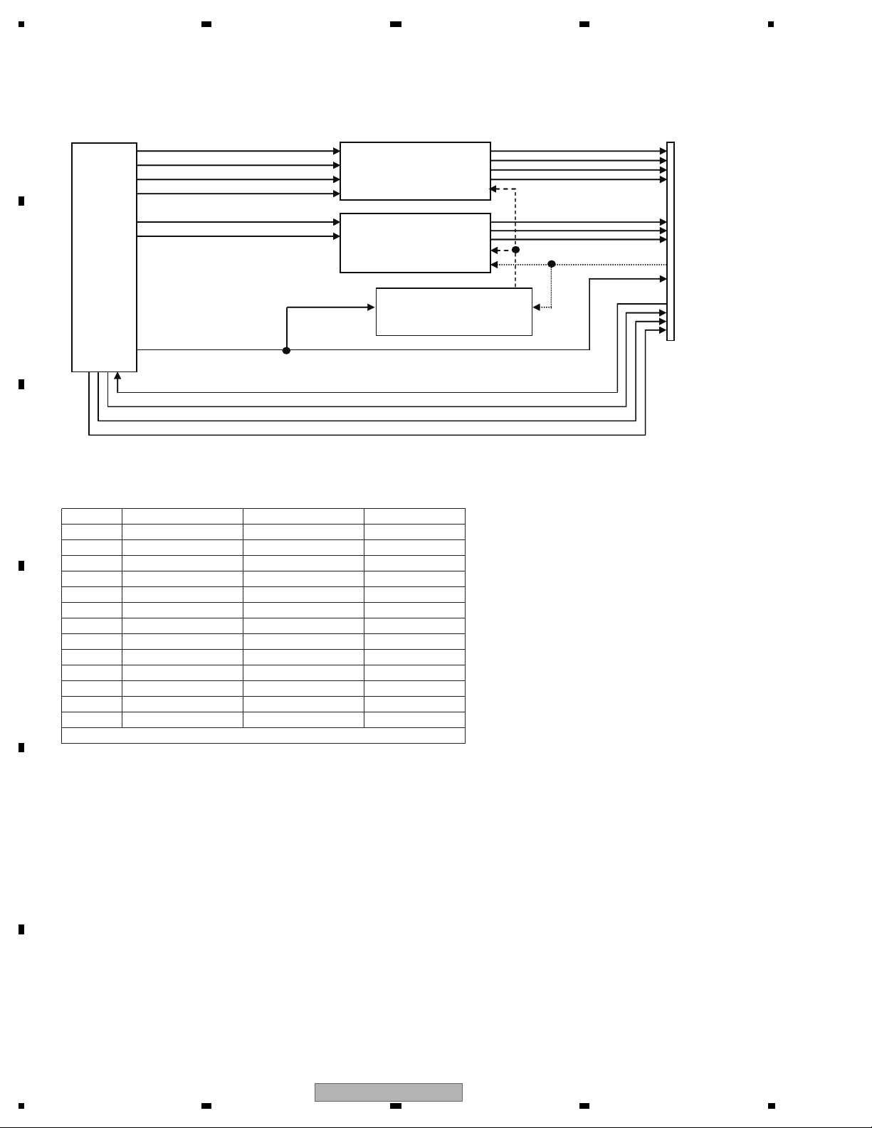
1234
<Outline> At the time of 6ch digital out, the serial 6 lines output from DVD-LSI (IC1501) is output via CN1581.
Furthermore, at the time of ripping, the serial 3 lines digital output + SUBC, output from DVD-LSI (IC1501),
is output in 4 times speed via CN1851.
A
CN1851
IC1501
LSI
ADOUT0/SUBC
ADOUT1/BLKCK
ADOUT2/CLDCK
IC1851 buffer SW,
ripping or 6ch digital out.
SRCK
LRCK
DATA
IC1852 buffer SW,
ripping or 6ch digital out.
MCKENA
B
IN IN
IC1853 buffer SW,
OUT
ripping or 6ch digital out.
RIPP
SBCK
BMUTE
EMPH
IEC/IPFLG
C
The signal at CN1851 for 6ch digital out/Ripping.
Pin No. Pin name
23
SRCK
21
LRCK
19
AD0/SUBC
17
AD1/BLK
15
AD2/CLD
13
AD3/DATA
11
IEC/IPFLG
9
-
D
7
SBCK
5
BMUTE
4
MCKENA
3
RIPP
2
EMPH
6ch digital out Ripping
SRCK
LRCK
ADOUT0
ADOUT1
ADOUT2
ADOUT3
IEC
-
BMUTE
Low
High
EMPH
SRCK
LRCK
SUBC
BLKCK
CLDCK
DATA
IPFLG
SBCK
High
Low
EMPH
Pins 1, 6, 8, 10, 12, 14, 16, 18, 20, 22 and 24 are GNDD.
Fig 10.7: 6ch digital out/Ripping circuit
E
F
50
1234
AVH-P5900DVD/XN/UC
Page 51
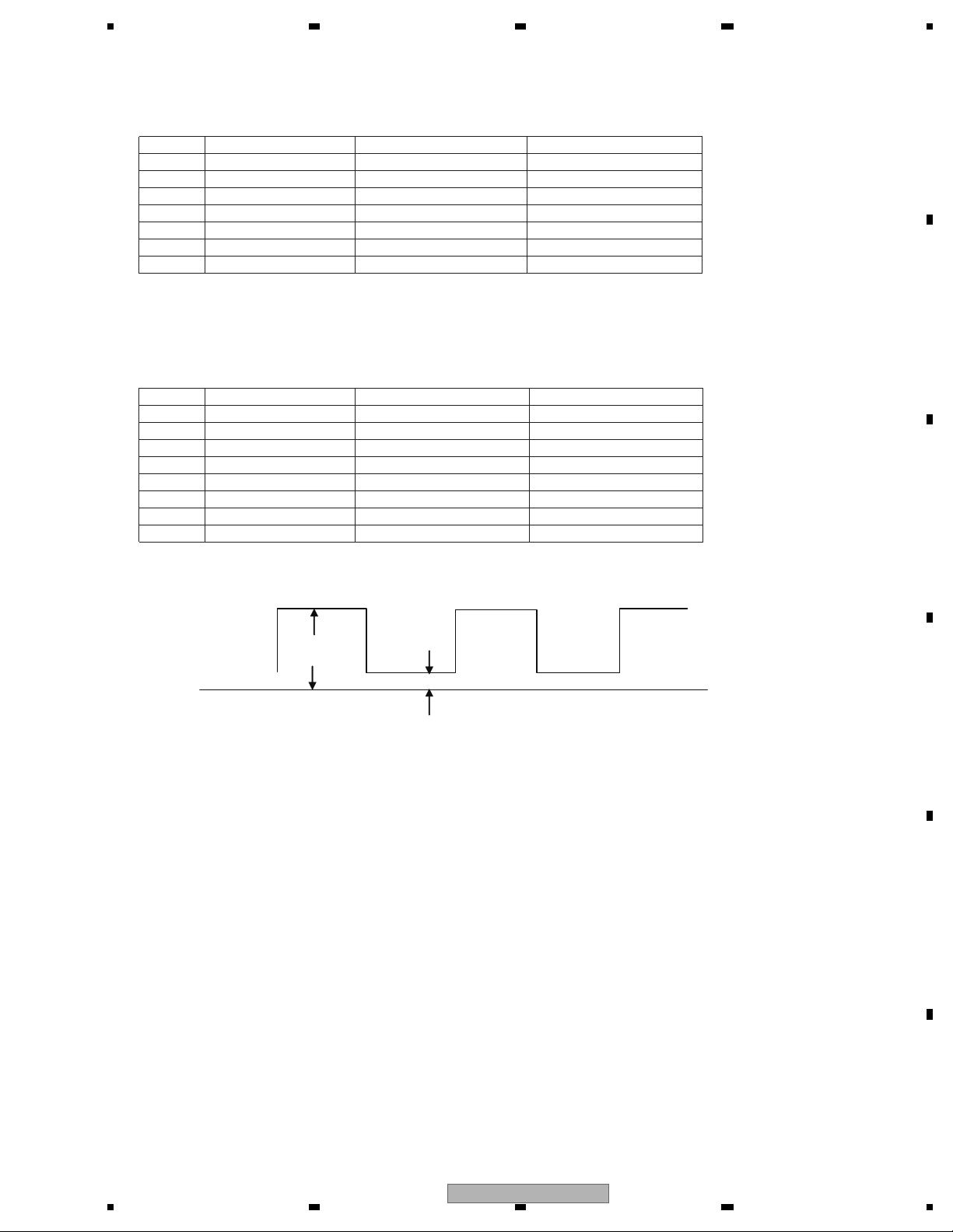
5 678
Playback DVD-REF-A1 TITLE22 CHAPTER 1, and check with GNDD being the reference.
In case of NG, check the applicable line, the periphery of the major components in the drawing above,
soldering of the peripheral components and defective components.
Check 24pin FFC after connecting it to a jig, etc.
NO. Check point 1 (stylus)
7
SRCK
8
LRCK
9
ADOUT0
10
ADOUT1
11
ADOUT2
12
IEC
13
MCKENA
Specification value 1
VCC33 V-0.6 V or higher
VCC33 V-0.6 V or higher
VCC33 V-0.6 V or higher
VCC33 V-0.6 V or higher
VCC33 V-0.6 V or higher
VCC33 V-0.6 V or higher
-
Specification value 2
0.4 V or lower
0.4 V or lower
0.4 V or lower
0.4 V or lower
0.4 V or lower
0.4 V or lower
VCC33 V x 0.3 V or lower
A
Rip common CDDA, and check with GNDD being the reference.
In case of NG, check the applicable line, the periphery of the major components in the drawing above,
soldering of the peripheral components and defective components.
Check 24pin FFC after connecting it to a jig, etc.
NO. Check point 1 (stylus)
14
SRCK
15
LRCK
16
SUBC
17
BLKCK
18
CLDCK
19
DATA
20
SBCK
21
RIPP
Specification value 1 Specification value 2
VCC33 V-0.6 V or higher
VCC33 V-0.6 V or higher
VCC33 V-0.6 V or higher
VCC33 V-0.6 V or higher
VCC33 V-0.6 V or higher
VCC33 V-0.6 V or higher
VCC33 V-0.6 V or higher
-
0.4 V or lower
0.4 V or lower
0.4 V or lower
0.4 V or lower
0.4 V or lower
0.4 V or lower
0.4 V or lower
VCC33 V x 0.3 V or lower
Specification
value 1
GND Specification value 2
Fig 10.8: 6ch digital out/Ripping specification value
B
C
D
56
AVH-P5900DVD/XN/UC
E
F
7
8
51
Page 52
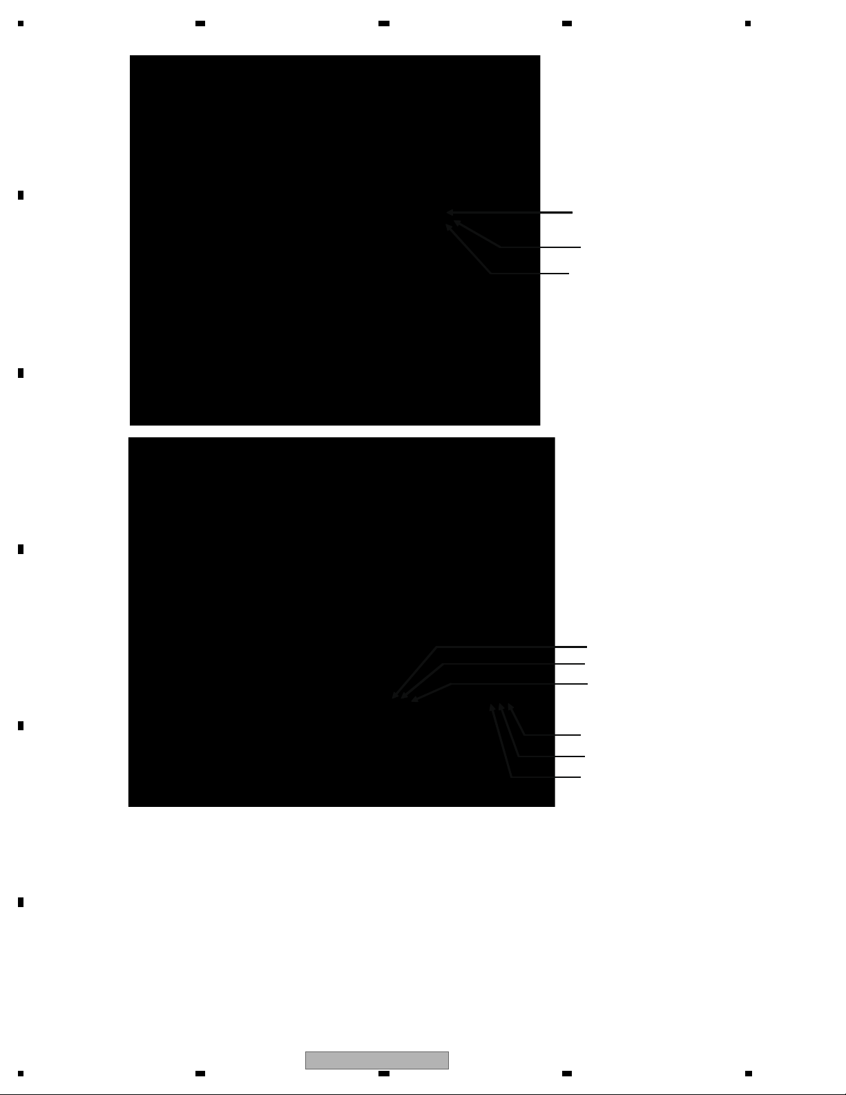
1234
SRCK
LRCK
ADOUT3
ADOUT2
ADOUT1
ADOUT0
RIPP
MCKENA
SBCK
Side A
A
B
Side B
C
D
E
Fig 10.9: 6ch digital out/Ripping check point
F
52
AVH-P5900DVD/XN/UC
1234
Page 53
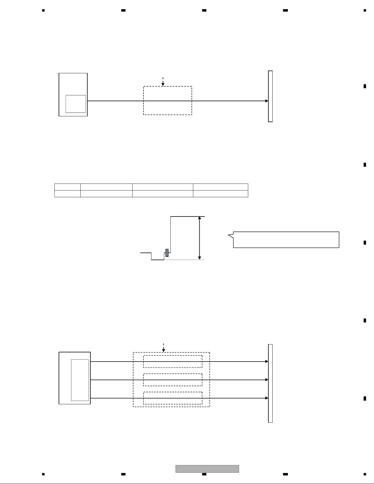
5 678
Check 11: Is the video circuit OK?
<Outline> Composite signal and component signal are output from DVD-LSI (IC1501), and are output from the
HOST I/F (CN1901) via a buffer circuit.
CN1901
HOST I/F
IC1501
DVD_LSI
Video
Composite
Component Y
Component Cb
Component Cr
AVCC5
Video buffer circuit
NoMount
COMPO
DAC
section
Fig 11.1: Video circuit
<Checking method> Playback DVD-REF-A1 TITLE2 CHAPTER5 (WHITE 100%), and monitor COMPO signal with
an oscilloscope with GNDV1 (stylus) being the reference. Set the trigger mode to “TV trigger” and
the trigger line to “150 line”.
Check point 1 (stylus)
NO.
Specification value Reference waveform
1 COMPO 1 000 mVpp ± 5 % Waveform 6
In case of NG, check the applicable line, the periphery of the major components in the drawing above, soldering of the
peripheral components and defective components.
PEAK
A
B
C
COMPO signal
Color burst
Reference
value
Adjust this level within the
range of 1.0 ± 0.02 Vpp.
Pedestal level
BOTTOM
Horizontal sync signal
Fig 11.2: Waveform for the case of composite white 100% output
<Video level readjustment method>
In case the video composite output is outside of the specification value, readjust the level according to the method
described below.(Note : Units are exchanged, the video output is not adjusted. )
Turn the volume (VR1671) to adjust the video level within the range of 1.0 ± 0.02 Vpp.
The adjustment specification is 1.0 ± 0.02 Vpp.
CN1901
IC1501
LSI
Video
DAC
AVCC5
YY
Q1701(NoMount)
Video buffer circuit
Cb Cb
Q1702(NoMount)
Video buffer circuit
HOST I/F
section
Cr Cr
Q1704(NoMount)
Video buffer circuit
D
E
Fig 11.3: Video circuit (component)
AVH-P5900DVD/XN/UC
56
F
7
8
53
Page 54
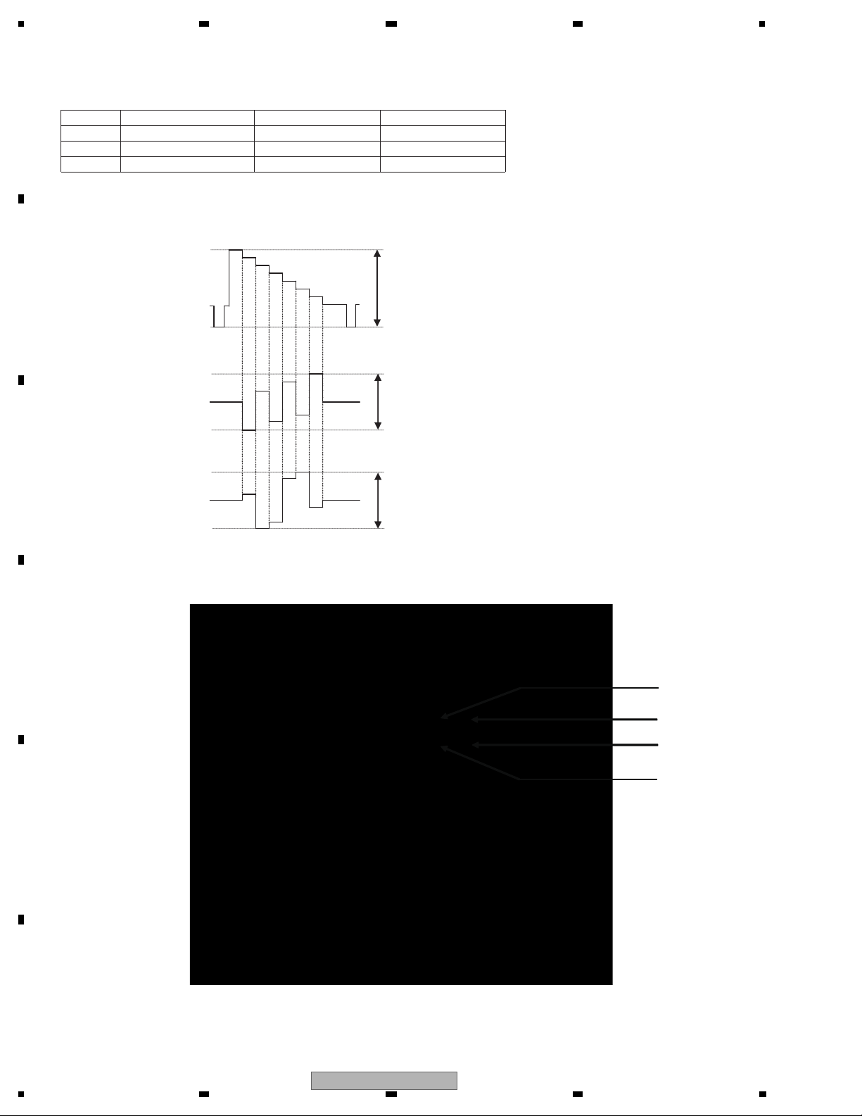
1234
Y
COMPO
Cr
Cb
<Checking method> Playback DVD-REF-A1 TITLE2 CHAPTER19 (100% Color Bars), and monitor Y, Cb, and Cr
signal with an oscilloscope with GNDV1 (stylus) being the reference. Set the trigger mode to
“TV trigger” and the trigger line to “150 line”.
A
NO. Check point 1 (stylus) Specification value Reference waveform
2
Y
3
Cb
4
Cr
1 000 mVpp ± 5%
700 mVpp ± 5%
700 mVpp ± 5%
Waveform 7
Waveform 7
Waveform 7
In case of NG, check the applicable line, the periphery of the major components in the drawing above, soldering of
the peripheral components and defective components.
PEAK
B
Y signal Specification value
BOTTOM
PEAK
Cb signal Specification value
BOTTOM
C
PEAK
Cr signal Specification value
BOTTOM
100% Color Bars signal
Fig 11.4 Waveform for the case of component 100% Color Bars output
Side A
D
E
F
54
Fig 11.5: VIDEO signal check point
AVH-P5900DVD/XN/UC
1234
Page 55

5 678
Check 12:How to judge whether the flash memory has reached its life or not.
If the reaction to user operation is slow or operation is slow in general, there is a possibility that the flash memory
has reached its life.
Make judgment regarding the flash memory life by looking at the display of the LD energizing time.
1.Let the LD energizing time displayed.
(Refer to the FE test mode for the method of displaying the LD energizing time.)
2.If the second digit from the left of the energizing time display is showing E,
such as “ E ”, it means that the flash memory has reached its life.
Example:
0E000BB8
A
B
C
D
E
F
56
AVH-P5900DVD/XN/UC
7
8
55
Page 56
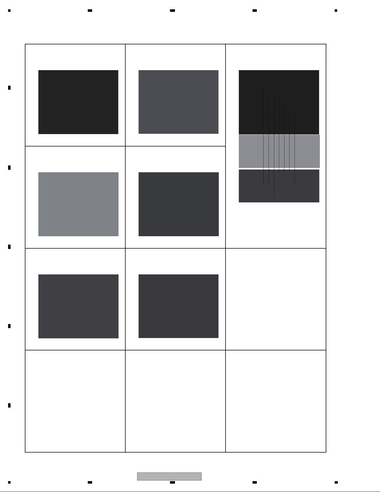
1234
AUDIO VIDEO
A
CH1 : ADOUT3 CH2 : RO
Reference voltage: DGND2 1 V/div. 5 μsec/div
G-> G->
B
Waveform 1 Waveform 4
CH1 : SRCK
Reference voltage: DGND2 1 V/div. 5 μsec/div Reference voltage: DGND2 1 V/div. 500 nsec/div
C
G->
CH1 : LO
Reference voltage: GNDAU2 1 V/div. 500 μsec/div
G->
CH1 : IECOUT
G->
[100% Color Bars]
CH1 : Y
CH2 : Cb
CH3 : Cr
Reference voltage: GNDV1 200 mV/div. 5 μsec/div
Waveform 7
Waveform 2
[WHITE 100IRE]
CH1 : LRCK
Reference voltage: DGND2 1 V/div. 5 μsec/div
D
G->
Waveform 3
E
CH1 : COMPO
Reference voltage: GNDV1 200 mV/div. 10 μsec/div
Waveform 5
Waveform 6
F
56
1234
AVH-P5900DVD/XN/UC
Page 57
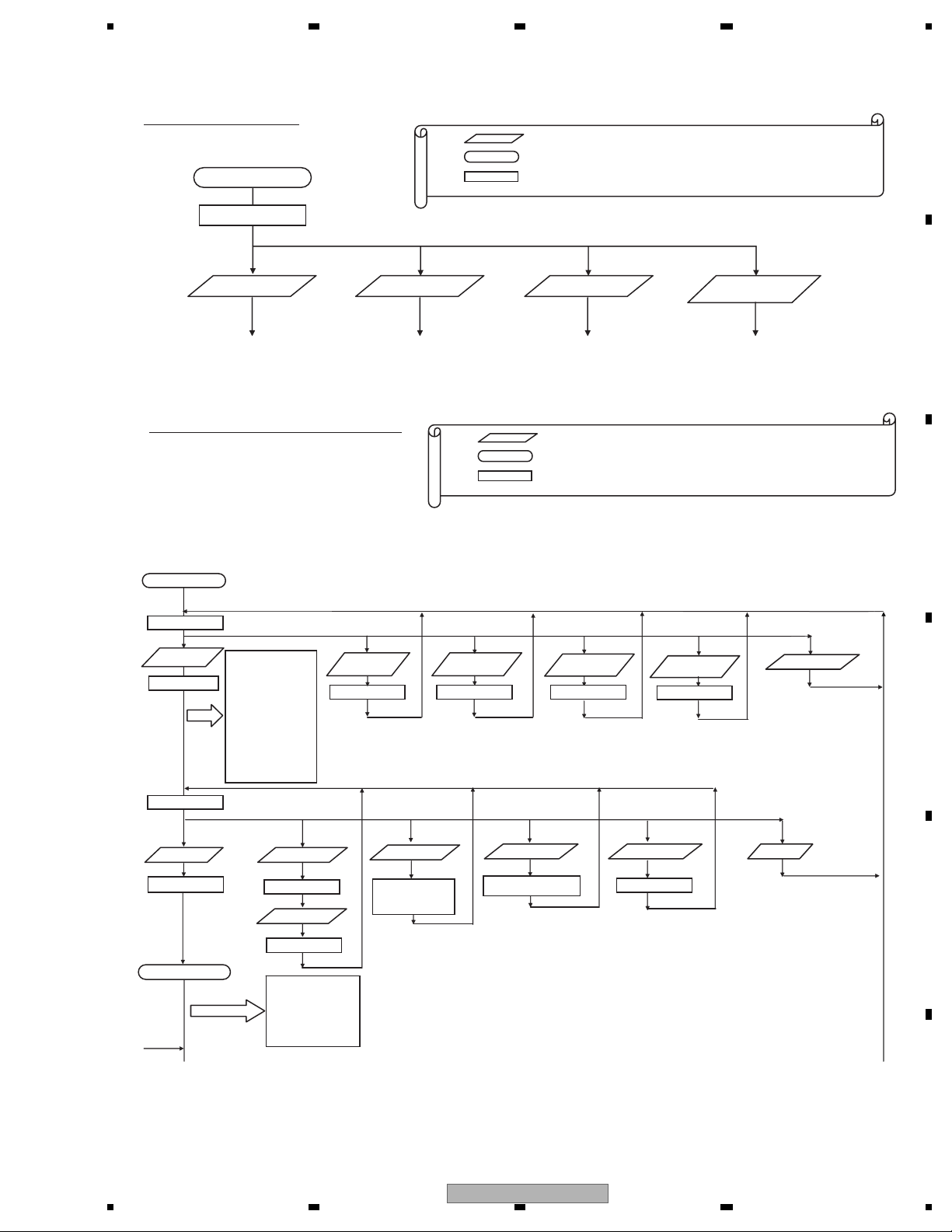
5 678
6. SERVICE MODE
6.1 DVD TEST MODE
Image of the test mode.
The following operations are done by remote control.
Start of the test mode.
TEST
[Note] Higher level 4 characters only. Lower level 4 characters are spaces.
(1) (2)
FE test selection EDC1 test selection
Hereafter, to FE test
mode image.
[Note] In order to move on to another test after selecting a test (FE/EDC1/EDC2), it is necessary to restart the DVD mechanism in the test mode.
Image of the front end test mode.
Legend:
Hereafter, to EDC1
test mode image.
Legend:
… Key operation
… Operation state
… The content displayed on the DVD mechanism (video only)
8 characters data is sent to the product side (HOST) by UART communication.
(3)
EDC2 test selection
Hereafter, to EDC2
test mode image.
(4)
LD power on time
mode selection
Hereafter, to LD power on
time mode image.
… Key operation
… Operation state
… The content displayed on the DVD mechanism (video only)
8 characters data is sent to the product side (HOST) by UART communication.
A
B
C
FE test mode
0 x 00 0000
(1)
Power on
0FFF 0000
1 x 00 0000
(1) (2)
F close F search
1FFF 0000
Focus close state
(2)
a b
FE offset coefficient
TE offset coefficient
AS offset coefficient
ENV offset coefficient
TG offset coefficient
DBAL coefficient
VIN1 offset cancel value
VIN2 offset cancel value
VIN3 offset cancel value
VIN4 offset cancel value
VIN5 offset cancel value
VIN6 offset cancel value
VIN7 offset cancel value
VIN8 offset cancel value
VIN9 offset cancel value
VIN10 offset cancel value
1A00 0000
(2)
F search
1100 0000
FEMAX level
FEMIN level
ASMAX level
ENVMAX level
FE normalization coefficient
Spindle gain coefficient
TEMAX level indication
TEMIN level indication
S curve
measurement
(2)
Disc type DVD1
layer
0000 0000
Activates while the key
1B00 0000 : CRG+
1C00 0000 : CRG-
(3),(4)
CRG+/-
is being pressed.
(3)
Disc type DVD2
layer
0100 0000 0200 0000
LD-ON/OFF
When LO-ON: 1100 0000
When LD-OFF: 1000 000
[Note] If no action is taken for approximately 10 seconds after LD-ON, it will become LO-OFF automatically.
If F close is selected during LD-OFF, it will become an error.
During focus search (S character measurement mode), too, safety regulation applies if LD_OFF is not selected
within 10 seconds. Therefore, even if focus search is selected after LD-ON, it will become LD-OFF after 9 seconds.
In order to F close after focus search (S character measurement mode), set to Power_OFF first then power on again
before F close.
Disc type CD
(5)
(4) (5)
Disc type CD-RW
0300 0000
(6)
CRG_HOME
1D00 0000
EJECT
EJECT
D
(8)
Power_OFF
E
56
AVH-P5900DVD/XN/UC
F
7
8
57
Page 58
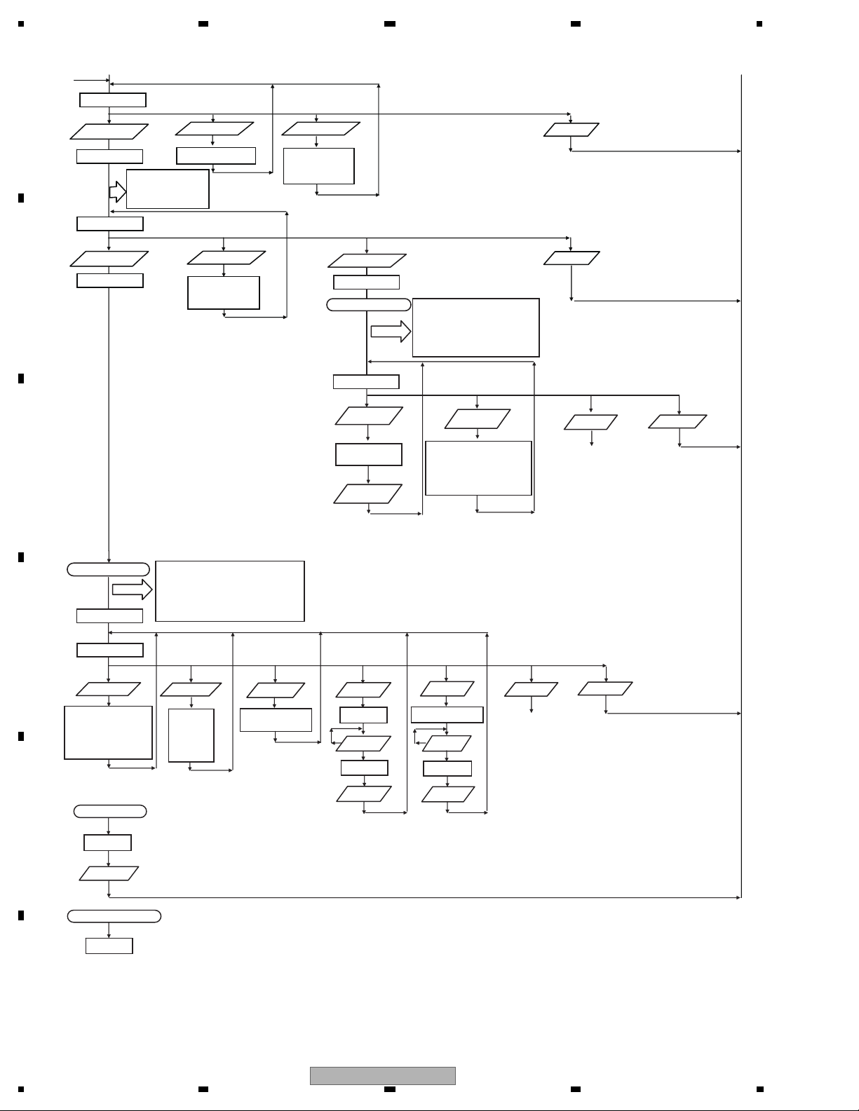
1234
(2)
A
B
C
a b
2 x 00 0000
(1)
Tracking balance
2FFF 0000
TBAL coefficient (layer 0)
TBAL coefficient (layer 1)
TE normalization coefficient (layer 0)
TE normalization coefficient (layer 1)
Off track adjustment result
3000 0000
(1) (3),(4)
Tracking close
3FFF 0000
Focus Jump
When L0 layer: 2000 0000
When L1 layer: 2100 0000
CRG +/-
It operates while the key
is being pressed.
3B00 0000 : CRG+
3C00 0000 : CRG-
(2)
(3),(4)
CRG +/-
It operates while the key
is being pressed.
2B00 0000 : CRG+
2C00 0000 : CRG-
Tracking close state
RF level is informed
(5)
RF level value
3FFF 0000
5000 0000
(1) (2)
RF level value
indication start
every 500msec.
(1)
RF level value
indication end
Performed including the tracking close processing.
FBAL coefficient (layer 0)
FBAL coefficient (layer 1)
Focus gain coefficient (layer 0)
Focus gain coefficient (layer 1)
Tracking gain coefficient (layer 0)
Tracking gain coefficient (layer 1)
AS normalization adjustment value (layer 0)
AS normalization adjustment value (layer 1)
Focus gain coefficient (layer 0)
Focus gain coefficient (layer 1)
Tracking gain coefficient (layer 0)
Tracking gain coefficient (layer 1)
AS normalization adjustment value (layer 0)
AS normalization adjustment value (layer 1)
Error rate
measurement
Error rate
(8)
Power_OFF
(8)
Power_OFF
(7) (8)
T.OPEN
To (2)
Power_OFF
Tracking close state
4000 0000
D
4 x 00 0000
(1) (2)
Error rate
measurement
Error rate
Focus gain coefficient (layer 0)
Focus gain coefficient (layer 1)
Tracking gain coefficient (layer 0)
Tracking gain coefficient (layer 1)
AS normalization adjustment value (layer 0)
AS normalization adjustment value (layer 1)
Error occurrence
E
Error display
(8)
Power_OFF
Error occurrence at Power_OFF
Error display
FBAL coefficient (layer 0)
FBAL coefficient (layer 1)
Focus gain coefficient (layer 0)
Focus gain coefficient (layer 1)
Tracking gain coefficient (layer 0)
Tracking gain coefficient (layer 1)
AS normalization adjustment value (layer 0)
AS normalization adjustment value (layer 1)
Playback speed
switching
DVDX1.3~
1.6CAV
CDX4CLV:
4x00 0000
L0 layer DVD X CAV,CD X 2CLV :4000 0000
L0 layer DVD X 1CLV,CD X 1CLV :4200 0000
L1 layer DVD X CAV :4100 0000
L1 layer DVD X 1CLV :4300 0000
V Change
V
L0 layer DVD X 1.3~1.6CAV, CD X 4CLV :4000 0000
L1 layer DVD X 1.3~1.6CAV :4100 0000
[Note] If an error occurs at Power_OFF, reset cannot be made. In such a case, it is necessary to turn the power off and start the test mode once again.
(5)
Focus Jump
When L0 layer: 4x00 0000
When L1 layer: 4x00 0000
(6) (3),(4)
ID Search
4A00 0000
(1)-(4) (3)
ID designation
ID display
(5) (5)
Search start
The number for designation of the track number shall be selected from the track numbers previously prepared.
Switch to cyclic by (3). Fix by (4).
For CD: Tracks 1, 4, 10, 11 and 32
For DVD: Tracks 1, 4, 10, 11, 32, 64 and 100
Change the method for ID address designation.
Designation of digit by command (1) and (2). UP/DOWN of numbers by command (3) and (4). Fix by command (5).
T.Jump+/-
Jump+ : 4B00 0000
Jump- : 4C00 0000
Track number
designation
Track number
indication
Jump start
(7) (8)
T.OPEN
To (2)
The higher 2 digits of the designated ID are the value showing the test state.
The lower 6 digits show the ID.
Example) If 300000 is desired to be designated as the ID, designated ID: 4A03 0000.
Power_OFF
F
58
1234
AVH-P5900DVD/XN/UC
Page 59
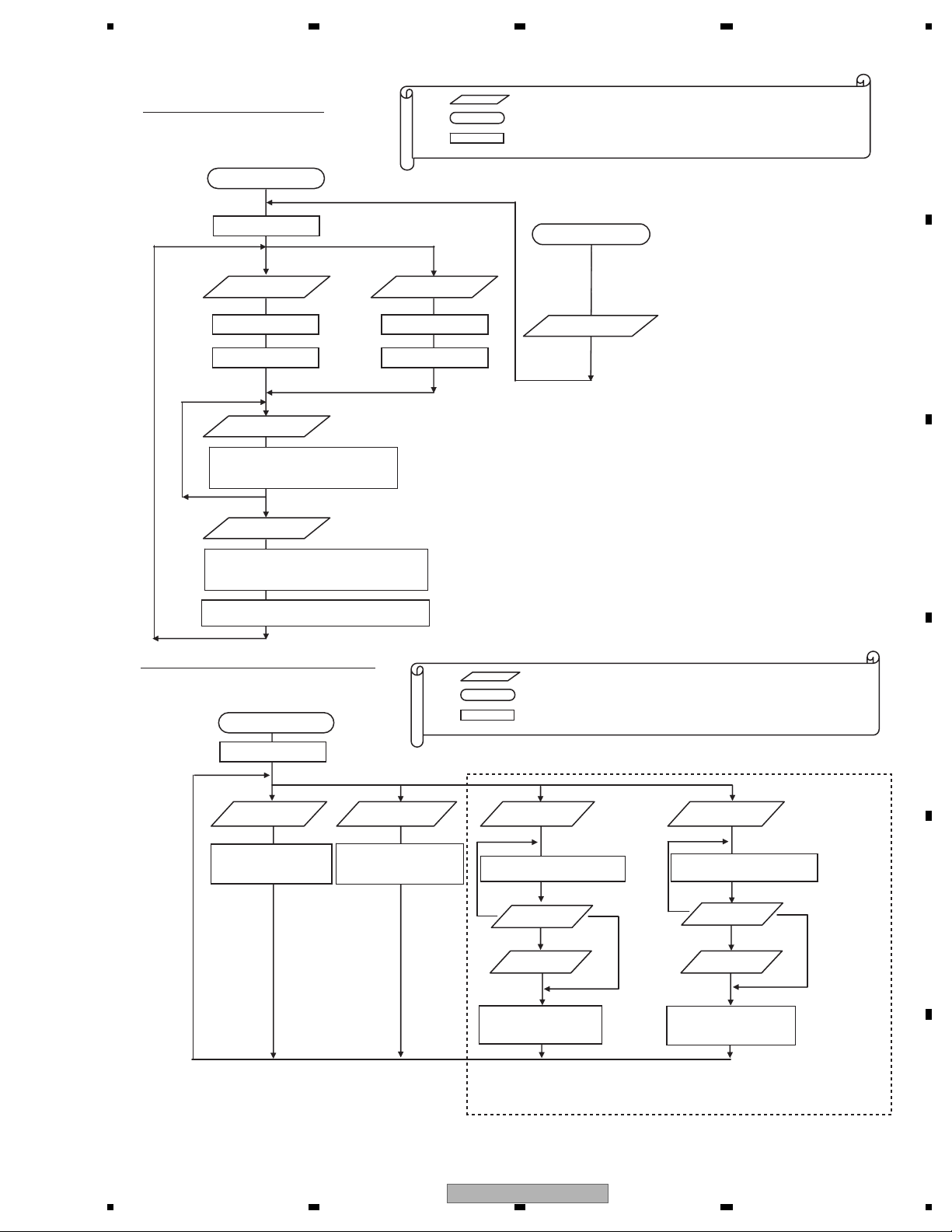
5 678
EDC. Image of the test mode
EDC1/2 test mode
0000 0000
(1) (2)
Layer 0 selection Layer 1 selection
0000 0000 0100 0000
1003 0000 1103 0000
(1)-(4)
ID designation
Layer 0: 10** ****
Layer 1: 11** ****
[Note] ** **** is the ID designation value
(5)
EDC1/2 start
Legend:
[Note] Image is the same for both EDC1 and EDC2.
… Key operation
… Operational state
… The content displayed on the DVD mechanism (video only)
8 characters data is sent to the product side (HOST) by UART communication.
EJECT operation
[Note] Eject can be effected any time during the EDC test mode.
Eject
Test mode Eject
After completion of EJECT operation
A
B
C
Layer 0: 20** ****
Layer 1: 21** ****
[Note] ** **** is the present ID designation value
**** ****
[Note] **** **** is the present ID designation value
Image of the LD power on time mode.
LD power on time mode
0000 0000
(1)
CD LD power on
time indication
10** ****
[Note] ** **** is the CD LD
power on time.
DVD LD power on
[Note] ** **** is the DVD LD
(2)
time indication
20** ****
power on time.
[Note] The display is updated at 0.5 seconds interval until 0/1 layer is selected or Eject is effected.
Legend:
… Key operation
… Operational state
… The content displayed on the DVD mechanism (video only)
8 characters data is sent to the product side (HOST) by UART communication.
Not for service use
(5)
CD LD power on
time setting
[Note] ** **** is the setting time.
(1)-(4)
30** ****
Setting time
designation
(5)
Setting time
registration
(8)
(6)
DVD LD power on
time setting
[Note] ** **** is the setting time.
(1)-(4)
40** ****
Setting time
designation
(5)
Setting time
registration
(8)
D
E
10** ****
[Note] ** **** is the CD LD
power on time.
[Method of setting time designation]
Designate the digit by command (1) and (2). UP/DOWN of numbers by command (3) and (4).
Fix by command (5). Cancel by command (8).
[Note] If the power on time is 999999 hours or more, it is always reported as 999999 hours.
[Note] If the power on time is “*E** ****”, the value may not be correct due to the life of the flash memory.
AVH-P5900DVD/XN/UC
56
7
20** ****
[Note] ** **** is the DVD LD
power on time.
F
8
59
Page 60
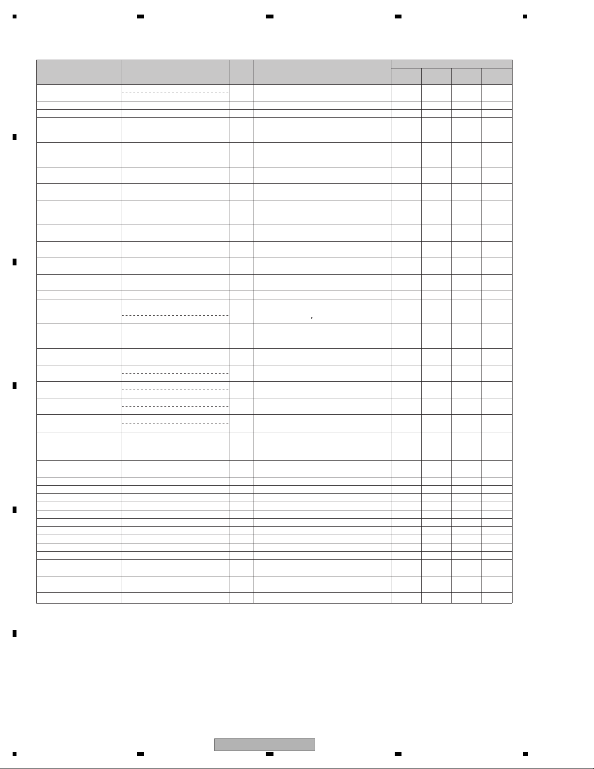
A
Media Error
Open
Read Error
Focus Error(Focus Error
in mechanism set up)
1234
Method of reset
ACC
Error status
It is a disc unable to be played back.
OSD *1
NON-PLAYABLE DISC
(No display)
ERROR-02-99
ERROR-02-90
UART
*2
A disc containing the unplayable Format only.
00h
10h
Door open error
20h
Transfer start error
21h
Focus error
Meaning
Off/On
Source
Off/On
****
XXXX
XXXX
Eject
X-XX
Play Key
Surface Error
Address not found
(Invalid Track)
Spindle Lock
B
Carriage HOME
ID/SUBCODE Read Error
AV CHIP decode Error
AV CHIP Recovery NG
Error of PLAY BACK Mode
Status
Disc Data Error
Temp Error
(In Case of High
Temperature)
C
No Disc
(including Disc loading
and ejecting)
Loading_Mecha Error 50h
DRM Error
Region code Error NG
CPPM*3 Key Error *4
AWM*5 Error *4
D
REQUEST error
Failure in issuing read
command (chip dependent)
Adjustment of L0 is NG.
Adjustment of L1 is NG.
LD system NG
Gain adjustment system NG.
Gain determining system NG.
Servo initial setting related items NG.
Disc is not clamped yet.
Tracking system NG.
Media setting system NG.
Focus Error
Error of PLAY BACK
Mode Status
E
Error of PLAY BACK
Mode Status
Undefined Error
X: Cancel the error by operation. -: Error is not cancelled by operation. *: No setting
*1 A content displayed on OSD. As for the items having multiple display patterns, the upper row is for the Japanese version Full GUI, and the lower row is for
the Touch Panel model and Full GUI (English version).
*2 A parameter of UART command, such as “receipt error notice”, that the DVD mechanism transmits.
*3 CPPM(Content Protection for Prerecorded Media) : A copyright protection technique used in DVD-A. The protection is realized by using the keys recorded
on the media and the device key held by the player.
*4 DVD-A compatible model only.
When an error has occurred, only the audio output will be muted but playback operation will continue. Furthermore, acceptance of the user operation will be
the same as usual.
*5 AWM (Audio WaterMark): Electronic watermark. Information on the copyright owner or CCI (copy control information) are recorded so that illegally copied
discs can be identified.
*6 Notice as an error status will not be given
*7 CPRM(Content Protection for Recordable Media) : A copyright protection technique for digital contents used for re-writable DVD or memory card.
F
(DVD-VR model only)
ERROR-02-9E
ERROR-02-80
ERROR-02-91
ERROR-02-92
ERROR-02-94
ERROR-02-9A
ERROR-02-9B
ERROR-02-9C
ERROR-02-9D
Temperature protection circuit is
being activated.
THERMAL PROTECTION IN MOTION
(No display)
(No display)
It is a protected disc.
PROTECTED DISC
Region code is incorrect.
DIFFERENT REGION DISC
It is a disc unable to be played back.
NON-PLAYABLE DISC
NON-PLAYABLE DISC
(No display)
ERROR-02-A0
ERROR-02-A1
ERROR-02-A2
ERROR-02-A3
ERROR-02-A4
ERROR-02-A5
ERROR-02-A6
ERROR-02-A7
ERROR-02-A8
ERROR-02-A9
ERROR-02-AA
ERROR-02-AB
ERROR-02-B0
ERROR-02-B1
ERROR-FF-FF
Focus error during set up
22h
(A focus has never been achieved with that
disc.)
23h
Address not found.
Spindle lock NG
24h
(the disc cannot rotate)
Carriage home NG
25h
(The pick up tries to return to carriage
home, but it cannot go back and stopped.)
ID/SUBCODE Read Error (ID/SUBCODE
26h
cannot be read due to scratch or stain.)
AV CHIP decode NG
2Ah
(AV chip cannot be decoded.)
2Bh
AV CHIP recovery NG
Playback state error
2Ch
(An error due to software bug.)
2Dh
Disc Data NG
High temperature
30h
(Playback is stopped because the pick up
temperature is 89 C or higher.)
Disc has not been inserted.
40h
(Including Load in process or Eject in process.)
Loading mechanism error
(The disc cannot be clamped.)
DRM error
70h
(All music cannot be played back due to DRM.)
Region code NG (Unable to be played back
90h
due to incorrect mechanism region.)
Key Error for playback
91h
93h Key Error for playback
Playback the illegally copied disc by DVD-A
*6
(Mute the sound on the mechanism side.)
A0h
REQUEST error
A1h
Failure in issuing the read command
A2h
L0 adjustment is NG.
A3h
L1 adjustment is NG
A4h
LD system NG
A5h
Gain adjustment system NG.
A6h
Gain determining system NG.
A7h
Servo initial setting related items NG.
A8h
Disc is not clamped yet.
A9h
Tracking system NG
AAh
Media setting system NG
ABh
JUMP over layers NG
B0h
Navigation command error
B1h
Retry over
FFh
Undefined error
XXXX
X
X
X
X
X
X
X
X
X
X
XXX -
X
X
X
X
X
X
X
X
X
X
X
X
X
X
X
X
X
X
X
X
X
X
X
-
*
-
-
--
- -X-CPRM Key Error *7
*
-
-
-
X
X
X
X
X
X
X
X
X
X
X
X
X
X
X
X
X
X
X
X
X
X
X
-
*
X
X
X
X
X
X
X
X
X
X
X
X
X
X
X
X
X
X
X
X
X
X
X
X
X
X
X
-
*
-
-
-
-
X
X
X
X
X
X
X
X
X
X
X
X
X
X
X
60
AVH-P5900DVD/XN/UC
1234
Page 61
5 678
7. DISASSEMBLY
Removing the Grille Assy and the Panel Unit
(Fig.1)
Push the [Detach] Button and then remove
1
the Grille Assy.
Remove the two screws and then
2
remove the Holder.
Disconnect the connector.
3
Remove the two screws and then
4
remove the Panel Unit.
Grille Assy
A
1
Holder
2
2
B
3
Panel Unit
4
4
C
- How to Separate the Upper Case and the
- Lower Case (Fig. 2)
Remove the seven screws.
1
Open the Upper Case and the Lower Case
2
in the direction indicated by arrows.
Upper Case
1
1
(Rear Side)
1
(Left Side)
Lower Case
(Right Side)
Panel
1
Fig.1
D
E
2
AVH-P5900DVD/XN/UC
56
1
11
F
Fig.2
7
8
61
Page 62
1234
A
Removing the DVD Mechanism Module (Fig.3)
Bracket
Remove the four screws and then bring
1
down the Bracket toward the Upper Case.
See Fig.3 (2/2).
2
2
1 1
Remove the four screws and then bring
2
down the DVD Mechanism Module toward
the Upper Case. See Fig.3 (2/2).
B
1 1
2
DVD Mechanism Module
C
2
Upper Case
Fig.3 (1/2)
Upper Case
D
Disconnect the three connectors.
3
3
3
E
3
DVD Mechanism Module
Mother Unit
Fig.3 (2/2)
F
62
1234
AVH-P5900DVD/XN/UC
Page 63
5 678
Removing the Holder and the Panel (Fig.4)
Remove the three screws.
1
Remove the three screws.
2
Remove the two screws and then remove
3
the Panel.
Remove the screw.
4
Straighten the tabs at two locations
5
indicated and then remove the Holder.
[Caution]
The Panel cannot be removed in unless
the Holder is removed in advance in
and .
5
3
4
3
1
2
1
A
1
2
3
2
Panel
Holder
5
B
4
5
C
Removing the Mother Unit (Fig.5)
Disconnect the connector.
1
Remove the two screws.
2
Remove the two screws.
3
Straighten the tabs at three locations indi-
4
cated and then remove the Mother Unit.
Fig.4
D
4
1
4
3
2
2
4
3
E
56
AVH-P5900DVD/XN/UC
Mother Unit
7
Fig.5
8
F
63
Page 64
1234
Removing the Monitor PCB 1/2 (Fig.6)
Remove the two screws and then remove
1
A
B
the two Guids(Right side and Left side).
Pull out the Monitor Assy in the direction
2
indicated by an arrow.
1
Bracket
1
2
Monitor Assy
C
Cover
Remove the three screws and then remove
3
3
the Cover.
Disconnect the connector.
4
D
E
4
3 3
Monitor Assy
F
64
1234
AVH-P5900DVD/XN/UC
Fig.6
Page 65
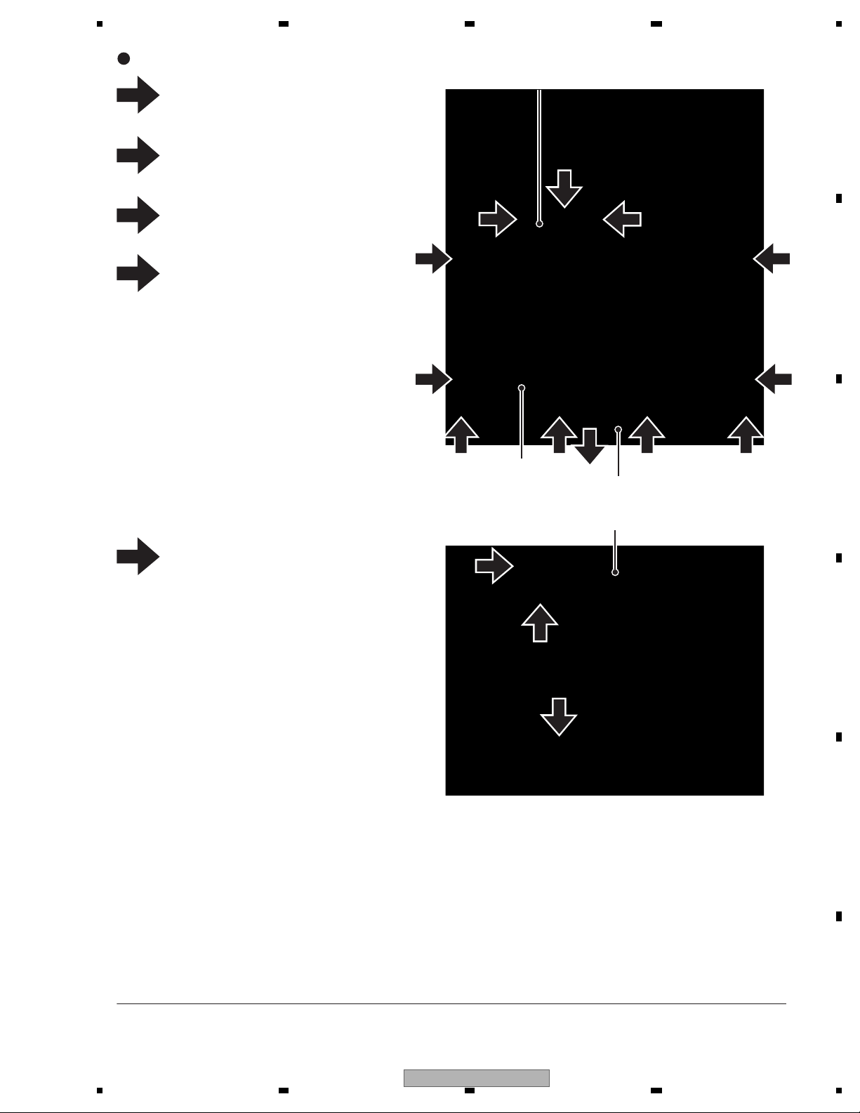
5 678
Removing the Monitor PCB 2/2 (Fig.7)
Remove the two screws and then remove
1
the Holder.
Remove the eight screws and then remove
2
the Monitor Assy.
Remove the Cover Unit.
3
4
Disconnect the connector.
[Caution]
The Monitor Assy cannot be removed
unless the Cover Unit is removed in
advance after removing the screws.
Holder
4
1
1
2 2
2
2 2 2 2
3
Monitor Assy
Cover Unit
A
B
2
C
Disconnect the three connectors and then
5
remove the Monitor PCB.
Monitor PCB
5
5
D
5
E
56
AVH-P5900DVD/XN/UC
Fig.7
F
7
8
65
Page 66
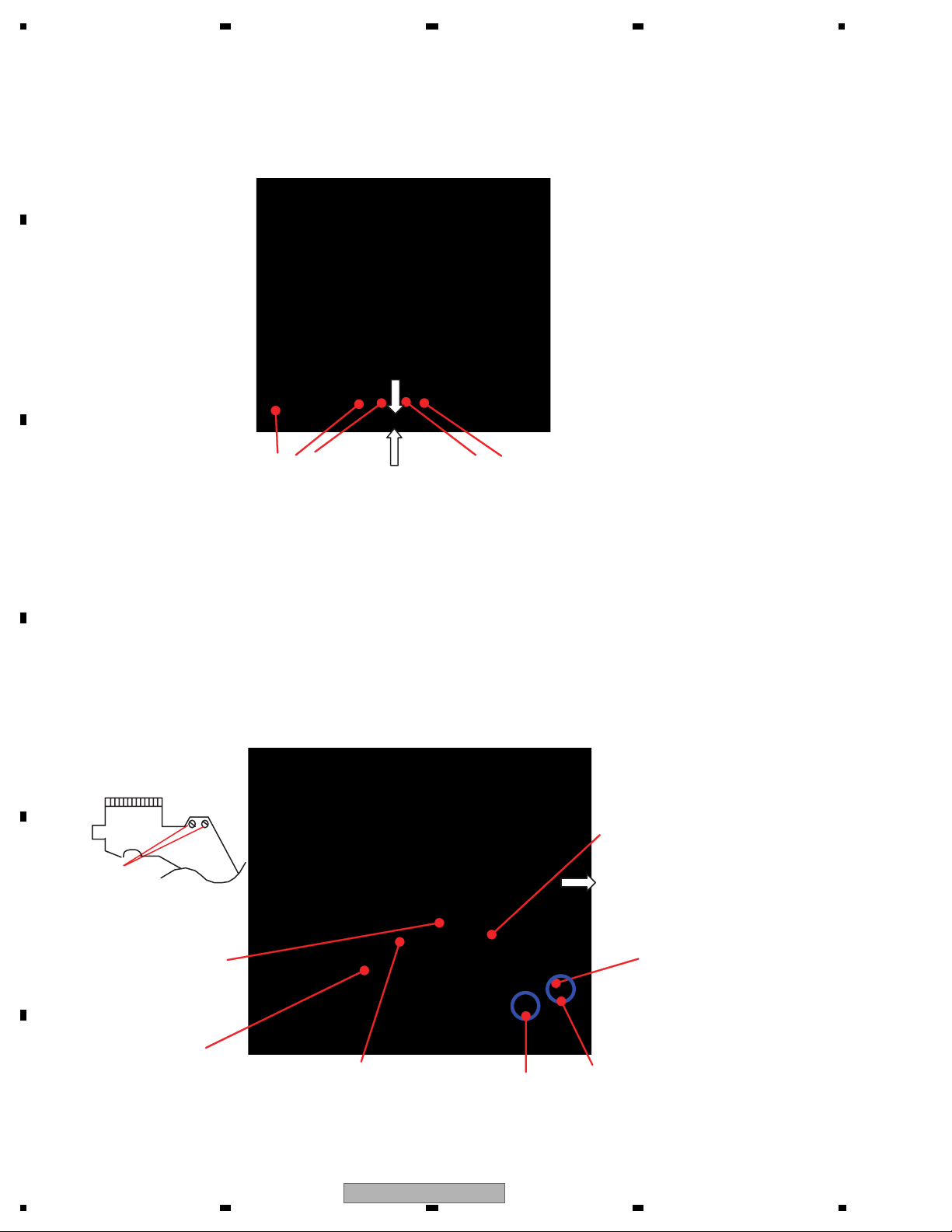
1234
- How to hold the mechanism section (Fig 1)
1. Hold the main frame and the top frame.
2. As the mechanical strength of the front part of the top frame is not strong, do not hold this part.
A
B
3. Do not touch the switches provided on the top face of the mechanism section.
4. Be careful not to pull the flexible PCB on the side face.
Fig 1
Do not touch this part. Do not touch this part.
Do not touch this part.
C
- How to remove the module PCB (Fig 2, Fig 3)
1. Put the mechanism section in locked state (disc load standby position).
2. Hold the mechanism module with its top face down.
3. Make the lands at 2 locations on the pick up flexible PCB short.
4. Disconnect the connectors of the pick up flexible PCB and the SPDL flexible PCB.
(Be sure to disconnect the connectors as the flexible PCB will be damaged if the PCB is removed without removing
the flexible PCB.)
5. Remove the solder joint of the lead wire of the load motor and the clamp SW.
D
E
6. Remove the two screws, and then remove the module PCB.
(Lift up point A slightly and remove it toward B direction. Be careful as the point C is connected with a flexible PCB.)
7. Disconnect the connector of the 8-12 detection flexible PCB from the PCB.
Fig 2
Module PCB
Short
Connector
(pick up flexible)
B
Connector
(8-12 detection flexible)
Solder land
(load motor, lead wire of the clamp SW.)
F
66
1234
Connector (SPDL flexible)
AVH-P5900DVD/XN/UC
A
C
Fig 3
Page 67
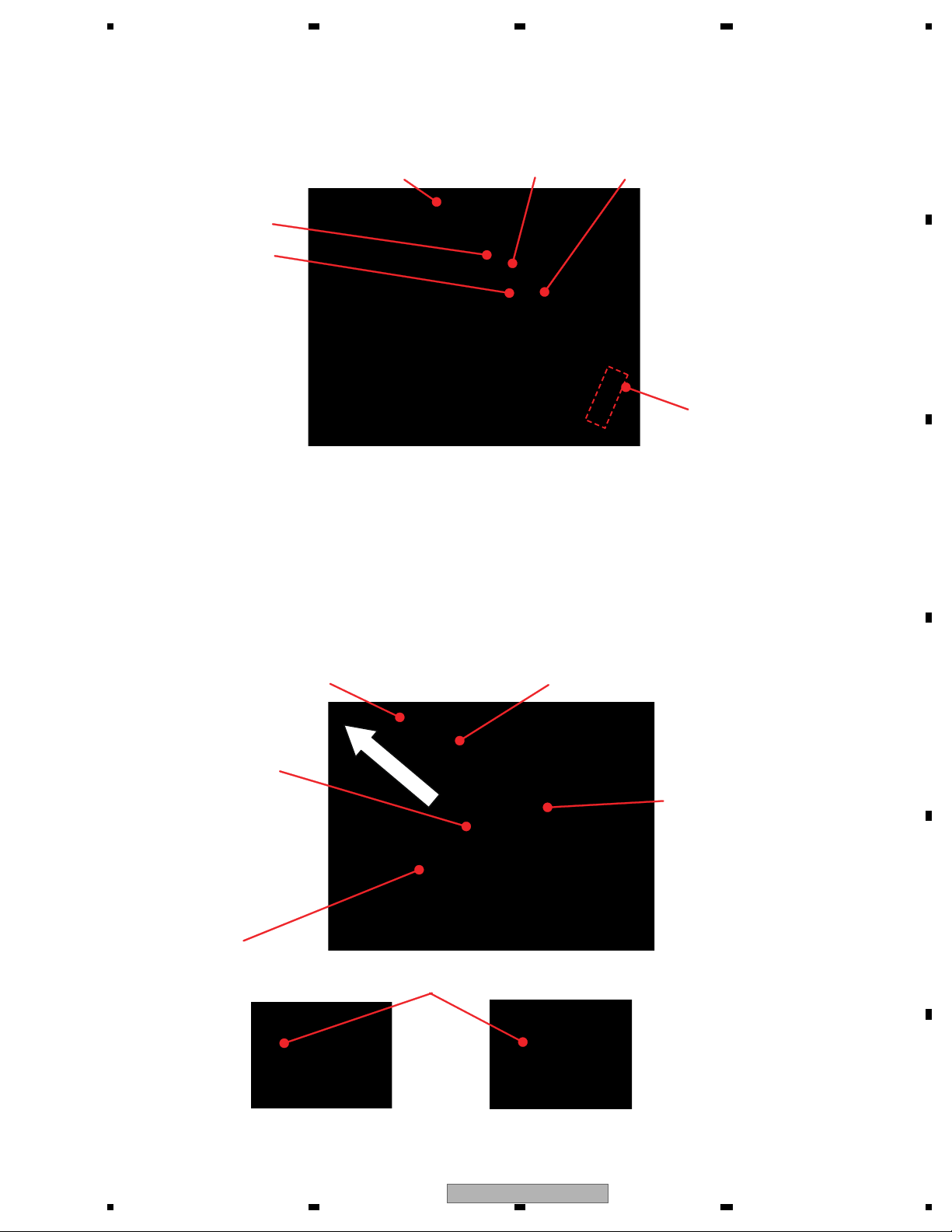
5 678
- How to remove the CRG motor assy (Fig 4)
1. Remove the module PCB according to the instructions in “How to remove the module PCB”.
2. Remove the Mylar tape.
3. Remove the flexible PCB of the CRG motor from the connector of the spindle motor.
4. Remove the two screws, and then remove the CRG motor assy.
A
Set screw (CRG)
CRG motor assy
Set screw (CRG)
Feeding screw
PU rack
Mylar tape
Fig 4
- How to remove the PU unit (Fig 5)
1. Remove the module PCB according to the instructions in “How to remove the module PCB”.
2. Hang the main shaft holding spring to the CRG chassis temporary hanger.
3. Remove the CRG motor assy according to the instructions in “How to remove the CRG motor assy”.
4. Remove the holding plate spring of the main shaft.
5. While lifting up the tip of the pick up rack, slide the main shaft, and remove the PU unit.
(Note) When mounting the PU unit again, make sure to do the adjustments of the devices mounted thereon
according to the descriptions of the service manual. Furthermore, make sure to hang the main shaft
holding spring permanently.
Holding plate spring
Main shaft
B
C
Sub shaft
PU unit
CRG chassis temporary hanging section
Temporary hanging
Permanent hanging
D
Main shaft holding spring
E
Fig 5
F
56
AVH-P5900DVD/XN/UC
7
8
67
Page 68

1234
8. EACH SETTING AND ADJUSTMENT
8.1 DVD ADJUSTMENT
A
1) Precautions
This product uses 5 V and 3.3 V as standard voltages.
The electrical potential that is the reference for signals,
is not GND, but VREF (approximately 2.2 V) and VHALF
(approximately 1.65 V) .
During product adjustments, if the reference voltage is
mistakenly taken as GND, and a grounding contact is
made, not only would it be impossible to measure the
B
accurate electrical potential, but also the servo motor
would malfunction, resulting in the application of a
strong impact on the pick up. The following precautionary measures should be strictly adhered to, in order to
avoid such problems.
The reference voltage and GND should not be confused
when using the minus probe of a measurement device.
When an oscilloscope is being used special care should
be taken to make sure that the reference voltage is not
connected to the probe of ch1 (on the minus side),
while the probe of ch2 (on the minus side), is connected
to GND. Further, since the body frame of most mea-
C
surement devices have the same electrical potential as
the minus side of the probe, the body frame of the measurement device should be set to floating ground.
If the reference voltage is connected to GND by mistake, turn the regulator OFF immediately, or turn the
power OFF.
Remove the filters and wires used for measurements
only after the regulator has been turned OFF.
After the power supply is turned on, regulator ON the
following adjustment and measurement are promptly
done.
Whenever the product is in the test mode, the software
will not take any protective action. For this reason,
special care should be taken to make sure that no
mechanical or electrical shock could be applied to the
product when taking measurements in the test mode.
Whenever the EJECT key is pressed to eject the disk,
no other keys, other than the EJECT key, should be
pressed until the disk eject action has been completed.
Press the EJECT key only after the disk has stopped
completely.
If the product hangs up turn the power OFF immedi-
ately.
Laser didoes may be damaged, if the volume switch for
the laser power adjustment of the pick up unit, is turned.
Attention)
Test mode starting procedure
Reset start while pressing the ATT
and RIGHT keys together.
Test mode stopping procedure
Reset or ACC OFF-ON.
D
E
F
68
AVH-P5900DVD/XN/UC
1234
Page 69
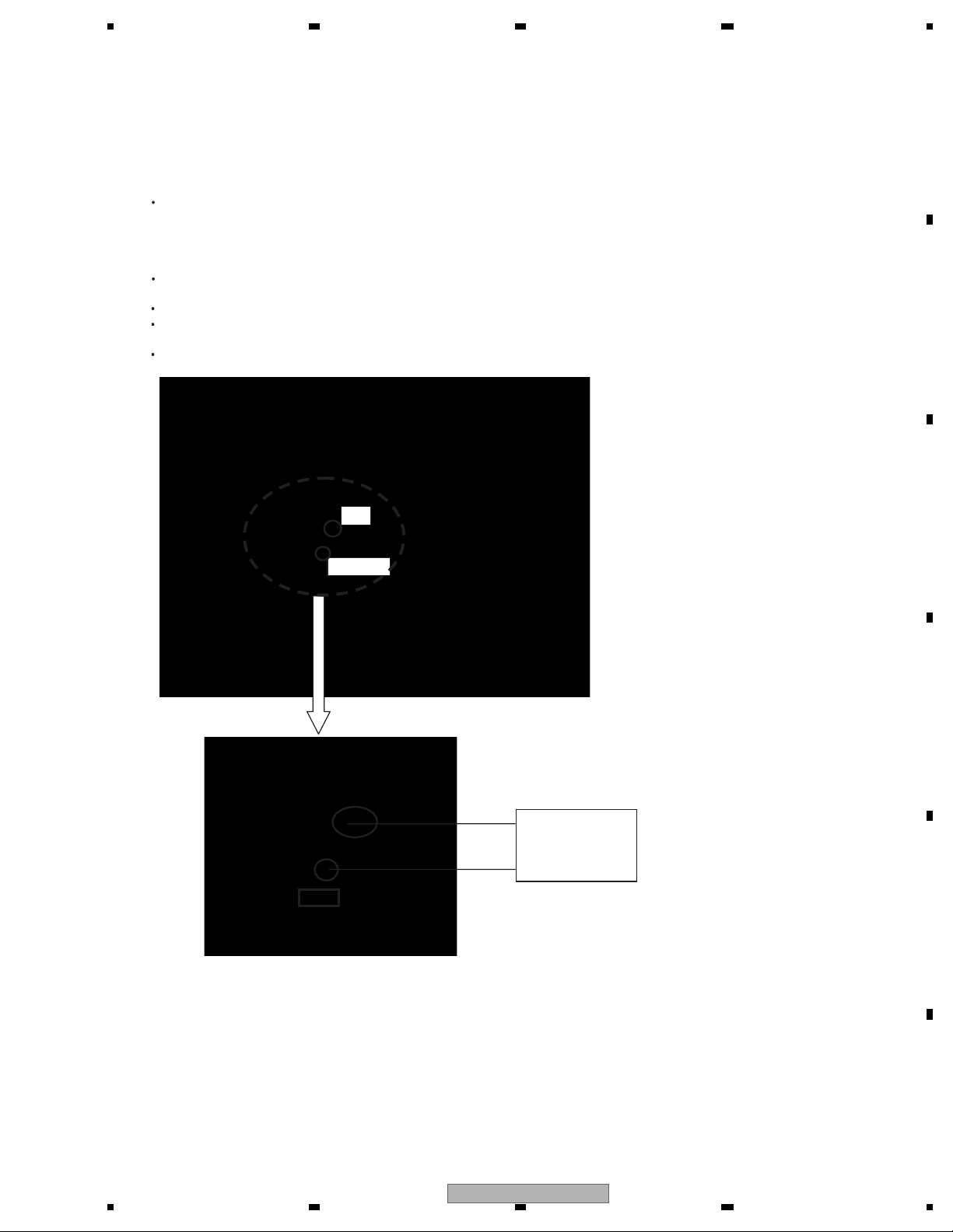
5 678
- SKEW adjustment
When one of the following replacements has taken place, SKEW adjustment for the pick up will be required.
(1) Replacement of the pick up unit
(2) Replacement of the spindle motor
(3) Replacement of the carriage chassis
(4) Replacement of the main shaft of the pick up unit
(5) Replacement of the sub shaft of the pick up unit
A
Measurement equipment and tools/jigs: Oscilloscope
Driver for SKEW adjustment t TORX driver (T2) (GGK1095)
Bond for fixing the SKEW (GEM1033)
Bond for locking the screw (Locking agents(1401M : produced by THREE BOND))
Disc used: GGV1018
Measurement reference: AGND2
Measurement point: RF
Connection drawing
DVD core unit
RF
AGND2
B
C
Enlargement
Oscilloscope
Symptom in case the adjustment is not adequate: Worsening of the error rate 10
(Normally 10-4 or less.)
Large RF jitter
RF waveform distortion
Tracking drawing/Unstable servo
* Caution: Do not look into the laser light during adjustment.
D
E
-3
F
56
AVH-P5900DVD/XN/UC
7
8
69
Page 70

1234
There are two methods for adjustment, a method whereby the adjustment is made while monitoring the RF waveform
A
using the oscilloscope (method 1) and a method whereby the adjustment is made while checking the RF level in
value by OSD (method 2).
The adjustment procedure is shown below. Refer to the paragraph for the service test mode regarding entering of the
test mode and the operation procedure.
Adjustment procedure:
1. Turn the DVD mechanism module upside down so that the pick up can be adjusted.
When the module is turned upside down, there is a possibility that the disc is rubbed.
So, first place a coin with the thickness of approximately 1.5mm on a desk, and set the module upside down in a
way that section 1 in the illustration below comes right above the coin.
B
2. Install the pick up. (Refer to the section regarding removal of the pick up from the mechanism unit.)
As for the precautions in handling the pick up, refer to the precautions in handling the PU as described below.
3. Method 1:
Connect the oscilloscope by referring to the connection drawing so that the RF signal can be monitored with
AGND2 as the reference.
Method 2:
There is no need for setting of any equipment. Proceed to step 4.
4. Turn the power ON, and load the disc for adjustment.(GGV1018)
C
the inner periphery. (CRG – Home)
6. Turn the LD ON.
7. Set to focus close, and make auto adjustment for all items under that state, then set to tracking close.
And make auto adjustment for all items under that state as well.
8. Make an intermediate periphery (ID: 100 000) search, and move the PU to intermediate periphery.
9. Method 1:
Proceed to step 10.
Method 2:
5. After setting the disc type to DVD layer 1 in the front end test mode, turn the power ON, and move the pick up to
D
After setting to Tracking Open, make all auto adjustments, and set to Tracking Close this time with a command that
can be RF displayed. Make auto adjustment for all items under that state as well.
10. Use TORX driver (T2) (GGK1095) for the following.
Method 1:
While monitoring the RF waveform on the oscilloscope, turn SKEW adjustment screw A just a little bit in a way that
the level will reach the maximum.
While the pick up is at the intermediate periphery, turn SKEW adjustment screw B just a little bit in a way that the
level will reach the maximum.
While the pick up is at the intermediate periphery, turn SKEW adjustment screw A just a little bit in a way that the
level will reach the maximum.
(Make adjustment in the order of A -> B -> A, Please end the each adjustment by turning screw clockwise. )
Method 2:
E
While monitoring the RF level value on the OSD display, turn the SKEW adjustment screw A just a little bit in a way
that the level will reach the maximum.
While the pick up is at the intermediate periphery, turn SKEW adjustment screw B just a little bit in a way that the
level will reach the maximum.
While the pick up is at the intermediate periphery, turn SKEW adjustment screw A just a little bit in a way that the
level will reach the maximum.
(Make adjustment in the order of A -> B -> A, Please end the each adjustment by turning screw clockwise. )
If the error is not good, please perform Method 1 again.
11. Turn the power OFF in the test mode, and after confirming that the disc has stopped, eject the disc.
12. Apply adhesive for fixing the SKEW and lock the screw.
Refer to the illustration below for the adhesion points.
F
70
1234
AVH-P5900DVD/XN/UC
Page 71
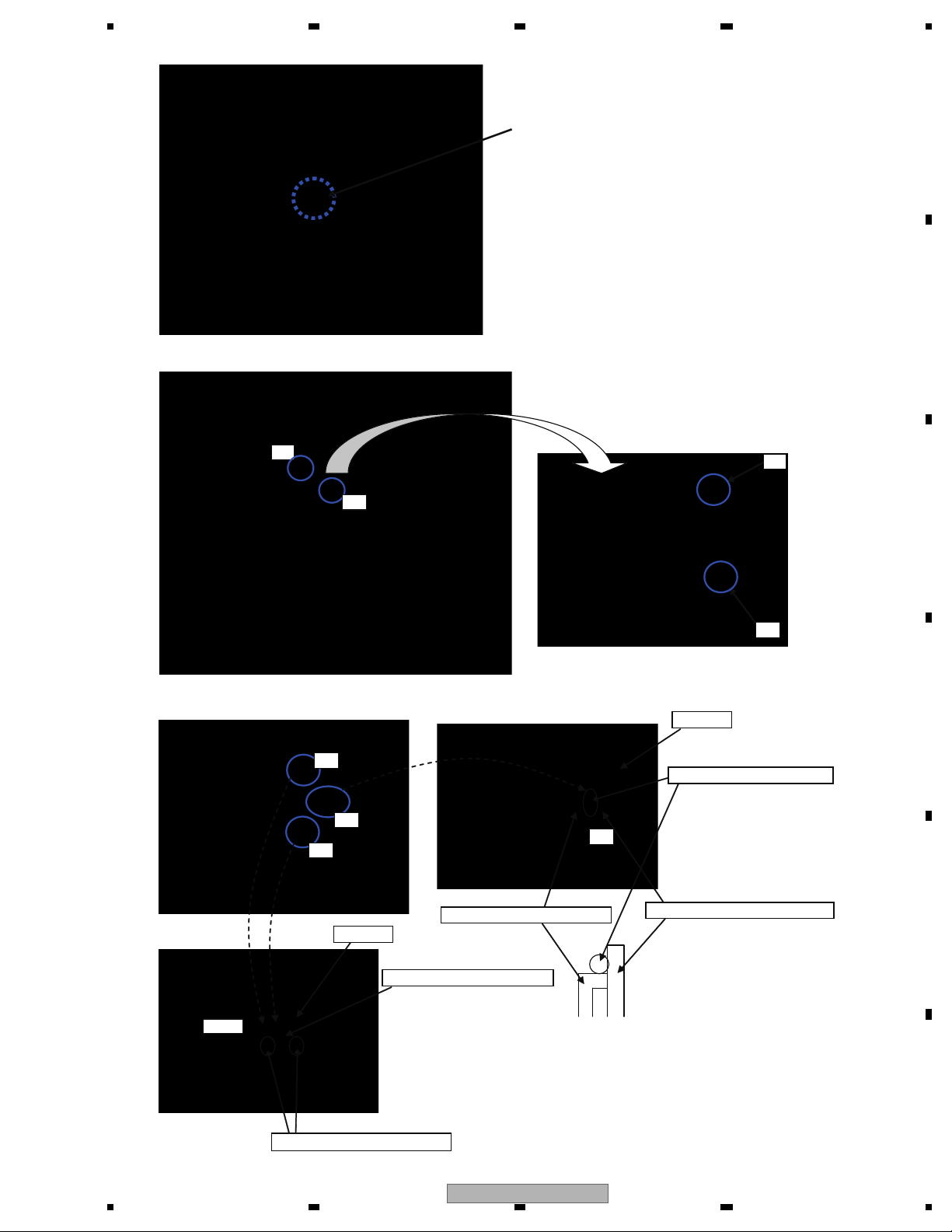
5 678
SKEW adjustment locations.
B
1
A
B
B
A
C
SKEW adhesive locations(GEM1033)
D
C
E
TAN-SKEW adhesive locations
PU case
D & E
RAD-SKEW adhesive locations
Sheet metal (yoke base) section
Sheet metal (yoke base) section
A
PU case
Adhesive application locations
C
Resin (suspension support) section
Cross section of R-SKEW adhesive locations.
* Caution: Make a cross link to both the resin section
and the sheet metal section.
D
E
Adhesive application locations
* Caution: Make a cross link to both the case section and the sheet metal section.
AVH-P5900DVD/XN/UC
56
F
7
8
71
Page 72
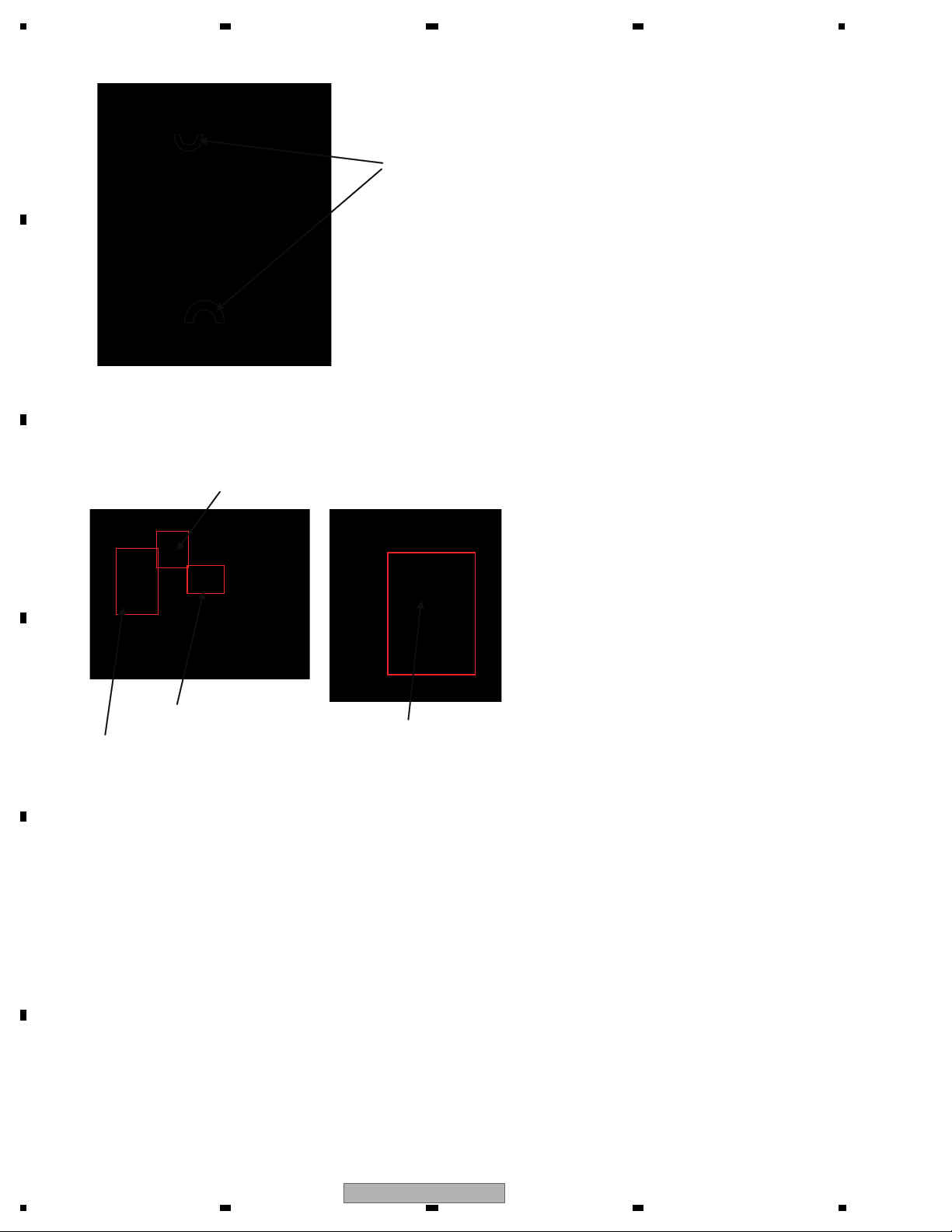
1234
Screw locking adhesive location(1401M : produced by THREE BOND)
A
Screw locking adhesive location
Apply the locking agent for more than half of the screw head
circumference.
* Caution: The locking agent shall not overflow to outside of
the PU case.
B
Precautions in handling the PU.
* Caution: Do not touch the shaded section in the drawing below.
RF level adjustment section
C
D
Do not touch the optical parts.
Do not touch the springs.
Hologram (be careful for the static electricity)
GRT adjustment section
E
F
72
1234
AVH-P5900DVD/XN/UC
Page 73
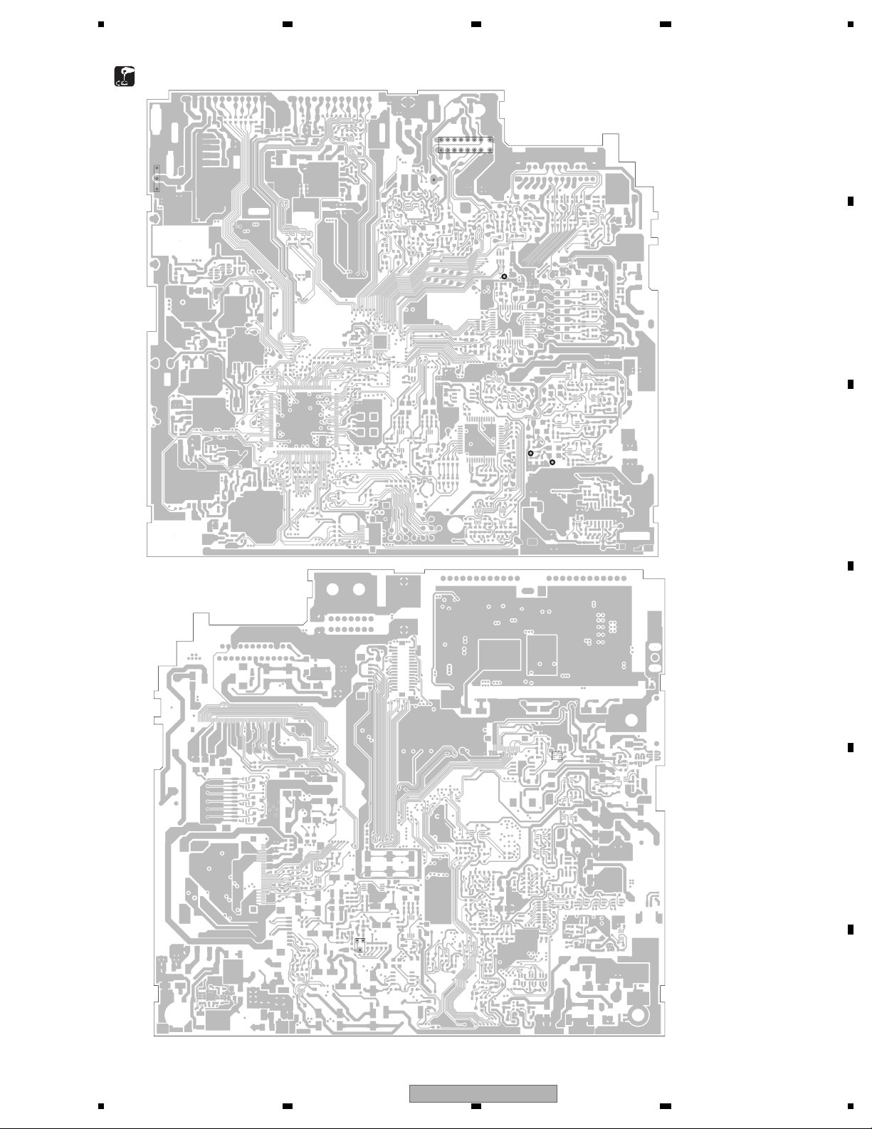
5 678
8.2 VIDEO LEVEL ADJUSTMENT
Adjustment point
Mother Unit(Side B)
1
1
1
A
MONVBS
B
TP395
TP396
C
Mother Unit(Side A)
D
E
1
VR271
56
AVH-P5900DVD/XN/UC
F
7
8
73
Page 74
1234
A
point
Adjusting
VR271
Specs
B
Measuring
C
±
1.35 V 0.05 Vp-p
Measure between the
sync tip and 100 IRE
instruments
(top wave).
Symptoms with
poor adjustment.
Over level :
Luminance is too high.
Under level :
Oscilloscope
Luminance is too low.
waveform)
Output signal
(measuring point,
Measuring point : MONVBS
D
100 IRE
Input signal
....
GND
....
other conditions)
(input test pin,specs,
Input test pin:
TP396
(white 100%),
1.0 Vp-p,
(input via 75 ohms)
TP395
(VIDEO GND)
E
Mode
adjustment
Mother PCB
AV
Main video level
F
Tuning of image output: Measure level at the measuring point as shown below while DVD is being replayed.
1
Step
74
1234
AVH-P5900DVD/XN/UC
Page 75
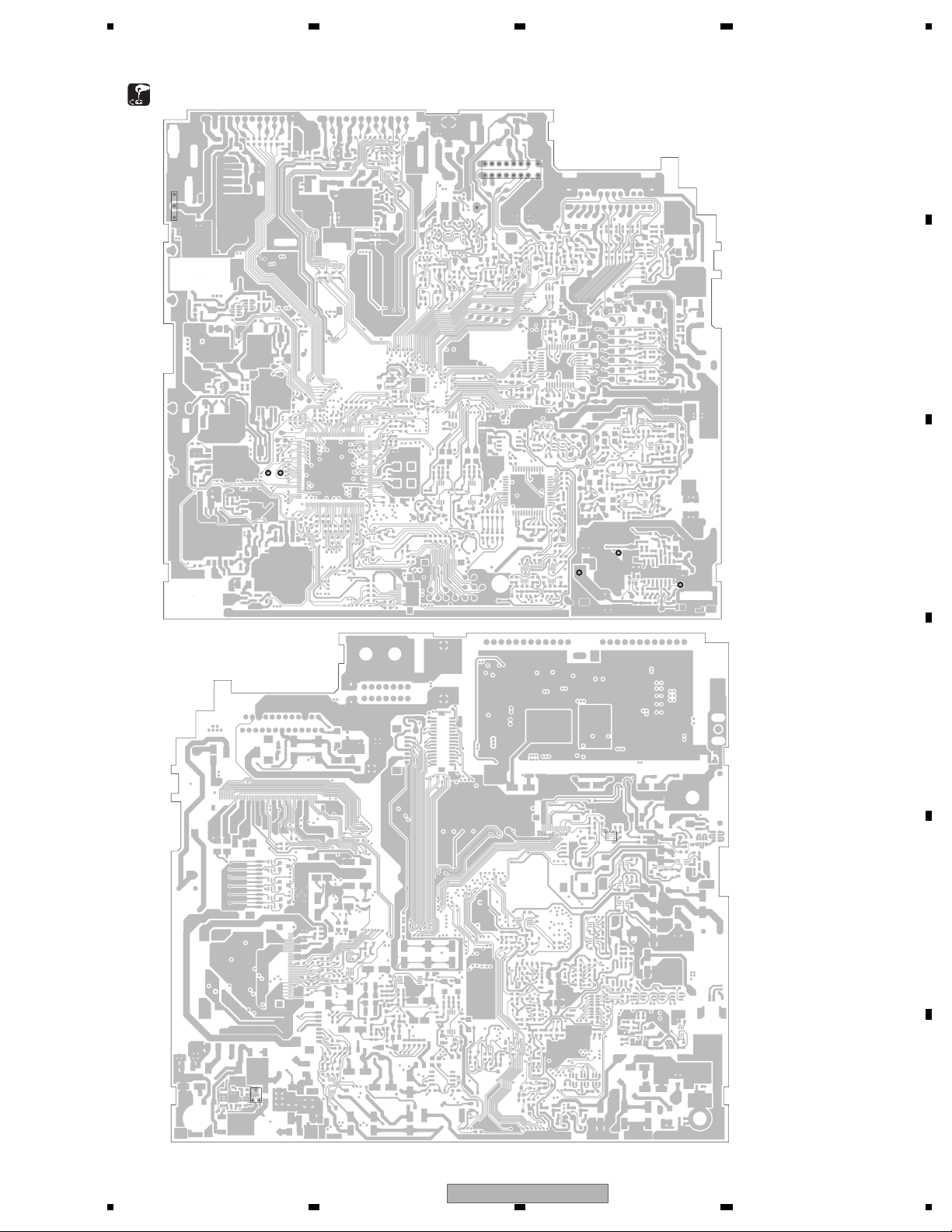
5 678
8.3 MOTHER UNIT ADJUSTMENT
Adjustment point
1
Mother Unit(Side B)
1
1
A
B
TP621
Mother Unit(Side A)
TP623
TP972
TP971
C
TP976
D
E
VR971
1
AVH-P5900DVD/XN/UC
56
F
7
8
75
Page 76
1234
A
point
Adjusting
±
754 Hz
Specs
B
18.874 368 MHz
Counter
Measuring
C
Frequency
instruments
±
5 kHz VR841
370 kHz
Counter
Frequency
waveform)
Output signal
(measuring point,
D
IC601 pin86(TP623)
TP976
Input signal
other conditions)
(input test pin,specs,
E
After the power supply
is turned on,
IC601 pin83(TP621)
to 3.3 V
Connect 33 Ω
(1.8 W or more) between
TP 972 and GND.
Connect 20 Ω
(1.2 W or more) between
TP 971 and GND.
Mode
adjustment
Mother PCB
Clock frequency
F
Check
Measure with the frequency counter at the measuring point as shown below while TUNER is turned ON.
1
DC-DC converter
frequency
Adjustment
2
Step
76
AVH-P5900DVD/XN/UC
1234
Page 77
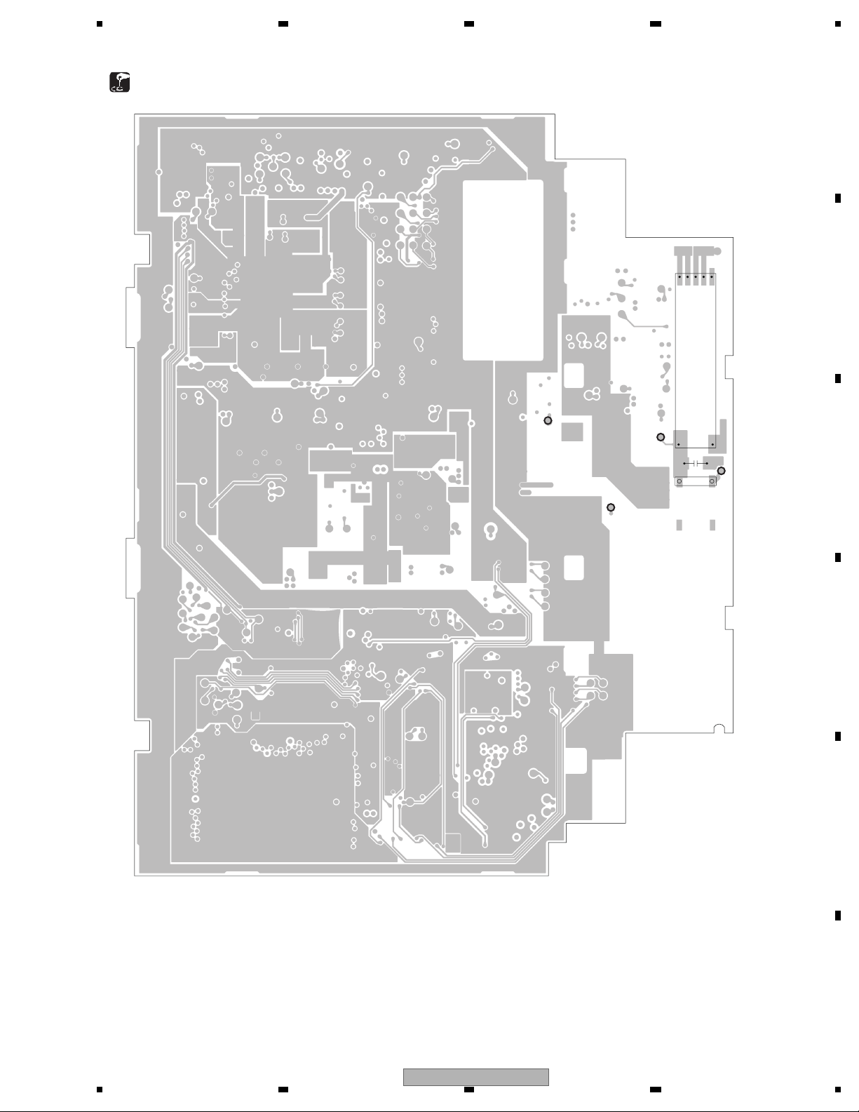
5 678
8.4 INVERTER ADJUSTMENT
Adjustment point
INVPUL
Monitor PCB(Side B)
1
5
T5201
FL1
C5225
1
FL2
A
B
C
PWRFL
CN5201
D
E
56
AVH-P5900DVD/XN/UC
F
7
8
77
Page 78
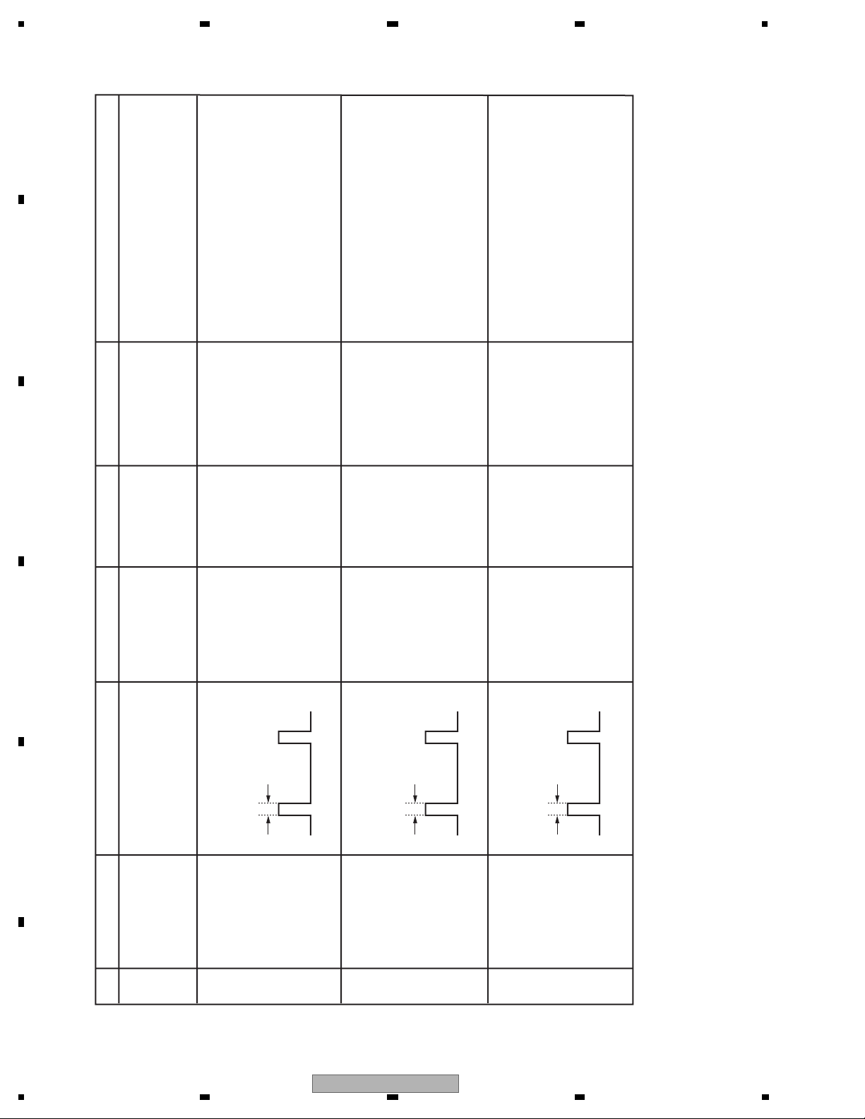
1234
A
Note
B
Verify that the frequency of waveform
Connect 100 kΩ between TP FL1 and FL2.
Monitor the waveform after voltage division or
TP FL2. Do not monitor TP FL1 directly
(measurement meter may be damaged
measured in No.1 is 49 kHz.
because of high voltage).
measured in No.1 is 51 kHz.
± 0.5 kHz
48.0 ± 0.1 kHz
C
49.0
-
51.0 ± 0.5 kHz
- Verify that the frequency of waveform
Verify that the frequency of waveform
measured in No.1 is 52 kHz.
± 0.5 kHz
52.0
-
VR5201
Adjustment point Adjustment
D
TP FL1
TP FL2
TP FL1
TP FL2
5 V
0 V
TP FL1
TP FL2
5 V
0 V
TP FL1
TP FL2
5 V
0 V
± 1 kHz waveform
E
±
14.4 0.2 V to TP PWRFL
TP DIMDTY : GND
TP FLGND : GND
TP INVPUL : GND
Basic drive
Frequency
adjustment
1
Instead of inserting LCD connector into CN5201, connect 100kΩ between TP FL1 and FL2.
F
78
No. Adjustment item Input signal Measurement point
Measure with the frequency counter at the measuring point as shown below.
1234
10
below to TP INVPUL.
Input 98.0
Check frequency
switching
2
AVH-P5900DVD/XN/UC
± 2%
± 2%
10
below to TP INVPUL.
Input 102.0 ± 1 kHz waveform
Check frequency
switching
3
± 1 kHz waveform
10 ± 2%
below to TP INVPUL.
Input 104.0
Check frequency
switching
4
Page 79
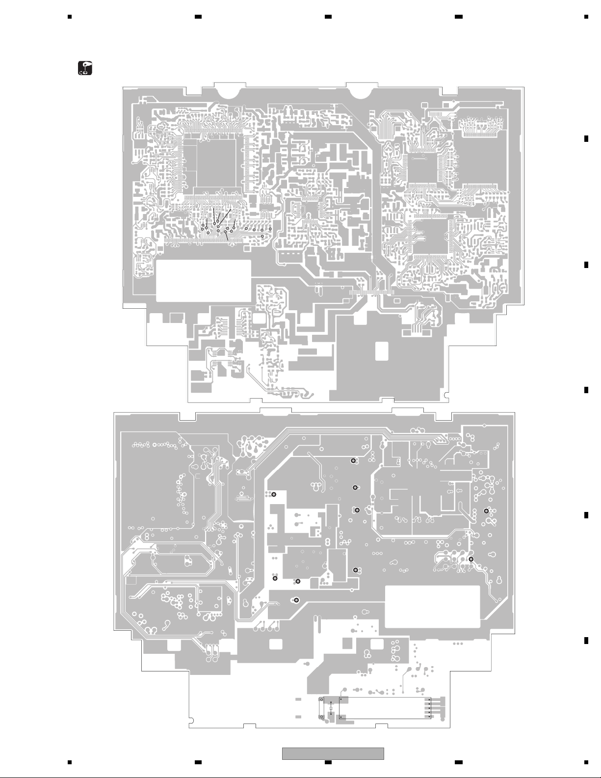
5 678
8.5 MONITOR ADJUSTMENT
Adjustment point
DC4
DC5
DC3
DC2
DB5
DB2
DB4
DA5
DA4
DB3
DA2
DA3
VD9
VD7
VD5
VD1
Monitor PCB(Side A)
A
B
VD3
C
33V
VCC8V
18V
PWRVI
V25
V15
-12V
Monitor PCB(Side B)
D
5V
COMPC
COM
E
CN5201
1
C5225
AVH-P5900DVD/XN/UC
56
T5201
7
5
1
8
F
79
Page 80
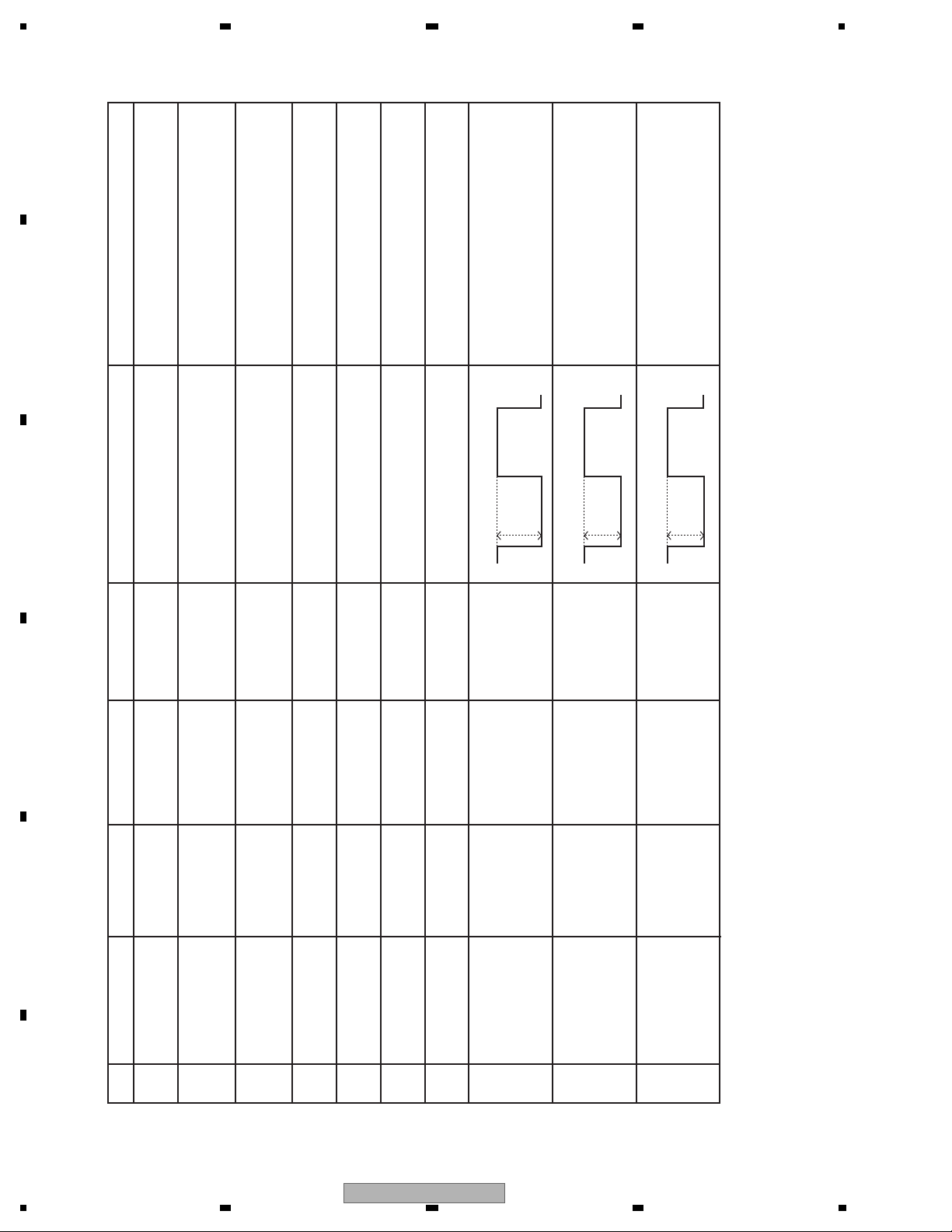
1234
A
Note
B
Connect LCD panel for measurement.
± 0.5 V
± 0.25 V
C
± 0.15 V
± 0.08 V
± 0.3 V
± 0.5 V
± 0.6 V7
± 0.30 V
33V = 3.3
4.70 ± 0.10 V
4.20
Connect LCD panel for measurement.-
± 0.10 V
1.75
-
Adjustment point Adjustment
D
TP:33V -
TP:V25 - V25 = 2.5
E
NOTE : When shutting off the power supply of TC90A96BFG-P, be careful not to energize each IC terminal. However, IIC lines (SDA and SCL) is not included in
this case and it is possible to energize them with up to 5 V.
F
80
TP:PWRVI
to 14.4 V
TP:PWRVI
Check 3.3 V power
supply voltage
1
No. Adjustment item Input signal Measurement point
1234
2 Check 2.5 V power
TP:V15 - V15 = 1.5
to 14.4 V
TP:PWRVI
to 14.4 V
supply voltage
supply voltage
3 Check 1.5 V power
TP:VCC8V - VCC8V = 8.0
TP:5V - 5V = 4.9
TP:PWRVI
TP:PWRVI
4 Check 5 V power
to 14.4 V
to 14.4 V
supply voltage
supply voltage
5 Check 8 V power
AVH-P5900DVD/XN/UC
TP:-12V - -12V = -12.0
TP:18V - 18V = 18.5
TP:PWRVI
to 14.4 V
TP:PWRVI
to 14.4 V
supply voltage
6 Check 18.5 V power
No definition. TP:COM -
Check -12 V power
supply voltage
Vcom amplifier
output amplitude
8
check
(TP:VD3)
No definition. TP:VD1 Connect LCD panel for measurement.
Tone voltage
amplitude
check V1
9
No definition. CN5501 55pin
Tone voltage
amplitude
check V3
10
Page 81
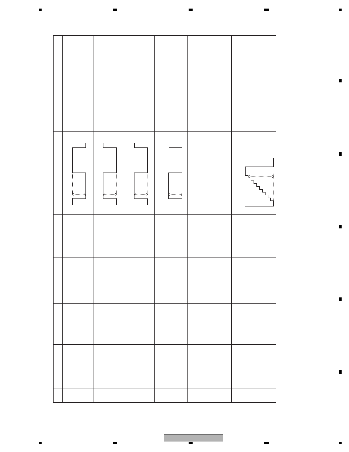
Note
5 678
A
B
and it measures it.
0.35 ± 0.10 V
-
Adjustment point Adjustment
It connects with the LCD panel
and it measures it.
± 0.10 V
0.60
and it measures it.
± 0.20 V
3.30
-
adjustment mode, LOW output is mixed to
the parts where there is a character.)
0.70 ± 0.05 V
-
--
The amplitude of the 9-step and
Resistor setting
1.77 ± 0.03 V
± 0.05 V.
C
the 0-step is 1.77
of SA13h D5 - 0
D
INo definitiont. TP:VD5 It connects with the LCD panel
Tone voltage
amplitude
adjustment V5
11
No. Adjustment item Input signal Measurement point
56
No definition. TP:VD7 -
Tone voltage
amplitude
adjustment V7
12
TP CCR,CCG,CCB (When OSD is displayed in EEPROM
Input white 100%
signal from
No definition. TP:VD9 It connects with the LCD panel
Tone voltage
amplitude
adjustment V9
13
IC5802
Check RGB digital
output
14
AVH-P5900DVD/XN/UC
Screen
Input Color-bar
signal from
IC5802
Image check of
RGB signal
15
DAC output
Input composite
image 10-step
Composite level
adjustment
16
7
± 1%)
signal to
TP MONVBS
(1.35 Vpp
E
F
8
81
Page 82
1234
A
Note
B
Brightness level of reverse signal should be 50%.
Adjustment point can be COM DC of flicker
digital-out is not bridged or “OPEN” ed.
Input white 100% signal
TP MONVBS (however, adjustment in RGB
comes first).
adjustment mode.
C
Make sure that tone changes
smoothly, and there is no colored
area in the entire display.
Leave for more than 30 minutes in
operation mode.
Adjust the flicker level to minimum
from all directions.
-
h in this chart means the sub-address of TC90A96BFG-P.
**
TP COMDC
Adjustment point Adjustment
D
Screen Execute to verify that IC5401
Measurement point
E
image lamp signal
(monochrome)
to TP MONVBS
DC output
Screen Black-white reverse signal can be the input to
reverse signal
per 1 line from
IC5802
SA
Image check Input composite
17
No. Adjustment item Input signal
F
82
1234
18 Aging No definition. - -
19 Flicker adjustment Input black-white
AVH-P5900DVD/XN/UC
Page 83
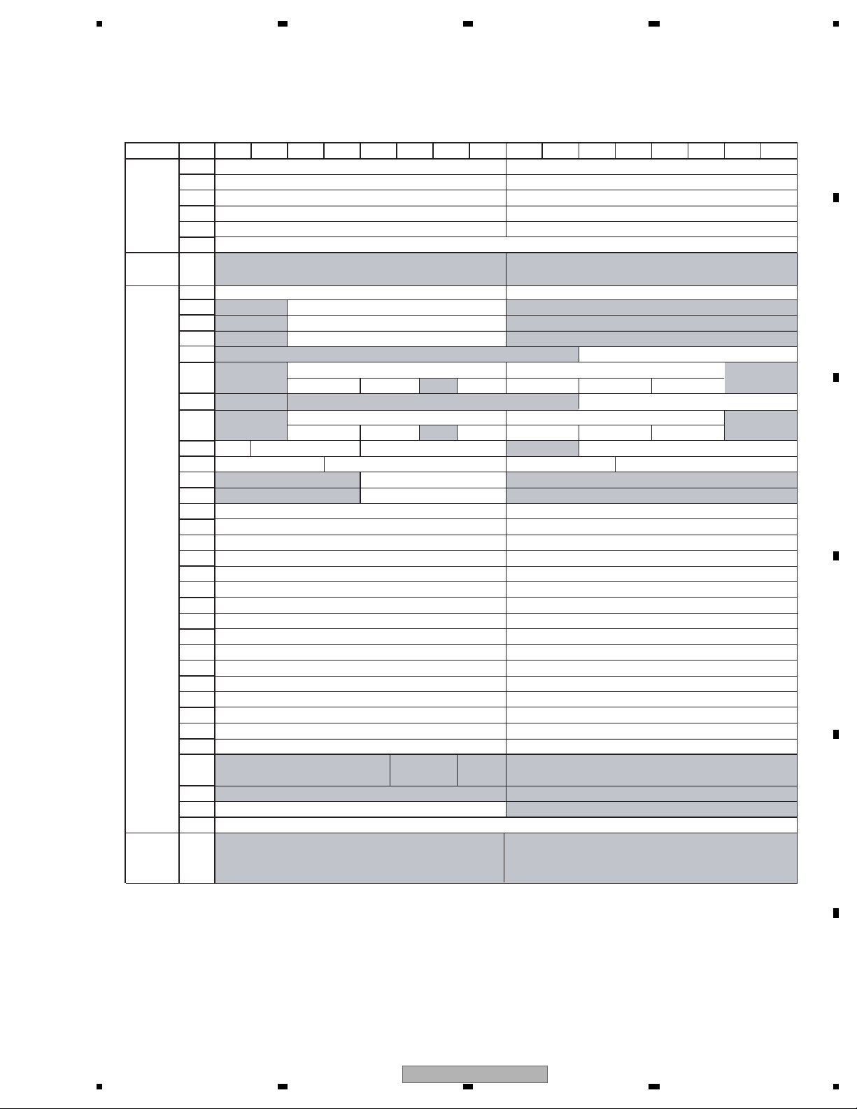
5 678
Memory item list and EEPROM
ADDRESS
Bit15 Bit14 Bit13 Bit12 Bit11 Bit10 Bit9 Bit8 Bit7 Bit6 Bit5 Bit4 Bit3 Bit2 Bit1 Bit0
00h Outside light of dimmer adjustment coordinates (high) Backlight of dimmer adjustment coordinates (high)
01h Outside light of dimmer adjustment coordinates (middle) Backlight of dimmer adjustment coordinates (middle)
RELATED
DIMMER
RELATED PIP
(
Dot adjustment
system
)
RELATED PIP
Last memory
(
value
)
RELATED PIP
Dot adjustment
(
system
--- Factory
shipment value)
02h
03h
04h
05h
06h 09h
0Ah
0Bh
0Ch
0Dh
0Eh
0Fh
10h
11h
12h
13h
14h
15h
16h
17h
18h
19h
1Ah
1Bh
1Ch
1Dh
1Eh
1Fh
20h
21h
22h
23h
24h
25h
26h 2Bh
2Ch,2Dh
2Eh
2Fh
30h 33h
Don't care
Don't care
Don't care
Don't care Don't care
Don't care Don't care
setting
γ
ON/OFF
RGB simultaneous slope B
Outside light of dimmer adjustment coordinates (low) Backlight of dimmer adjustment coordinates (low)
Outside light threshold for dimmer (high) Outside light threshold for dimmer (low)
Maximum value of backlight output Minimum value of backlight output
Common reverse output DC center value Common reverse output amplitude adjustment value
Gain Limiter Gain Replicate Cor ingfo
Gain Limiter Gain Replicate Cor ing
RGB simultaneous slope A
γ
Don't care
Don't care
Don't care
Checksum
Don't care Don't care
Brightness R
Brightness G
Brightness B
Don't care
Main horizontal enhancer
Don't care
Sub horizontal enhancer
fo
γ γ
RGB simultaneous 2 inflection point
SA24h UPPER
SA25h UPPER
SA26h UPPER TV
SA26h UPPER
SA27h UPPER TV
SA27h UPPER
SA46h UPPER
SA47h UPPER
SA48h UPPER
SA49h UPPER
SA4Ah UPPER SA4Ah LOWER
SA4Bh UPPER SA4Bh LOWER
SA4Ch UPPER
SA4Dh UPPER
SA4Eh UPPER
SA4Fh UPPER
Don't care
Flicker adjustment result
Don't care Don't care
R output DC offset
G output DC offset
B output DC offset
Main SYNC IN
sampling
Main PLL3
gain down
Don't care
RGB simultaneous slope C
Checksum
Main vertical enhancer
Sub vertical enhancer
γγ
Main Y contrast
Sub Y contrast
RGB simultaneous 1 inflection point
RGB simultaneous 3 inflection point
Don't care
Don't care
SA24h LOWER
SA25h LOWER
SA26h LOWER TV
SA26h LOWER
SA27h LOWER TV
SA27h LOWER
SA46h LOWER
SA47h LOWER
SA48h LOWER
SA49h LOWER
SA4Ch LOWER
SA4Dh LOWER
SA4Eh LOWER
SA4Fh LOWER
Main H-PLL3
Don't care
Don't care
A
B
γ
C
D
E
56
AVH-P5900DVD/XN/UC
F
7
8
83
Page 84
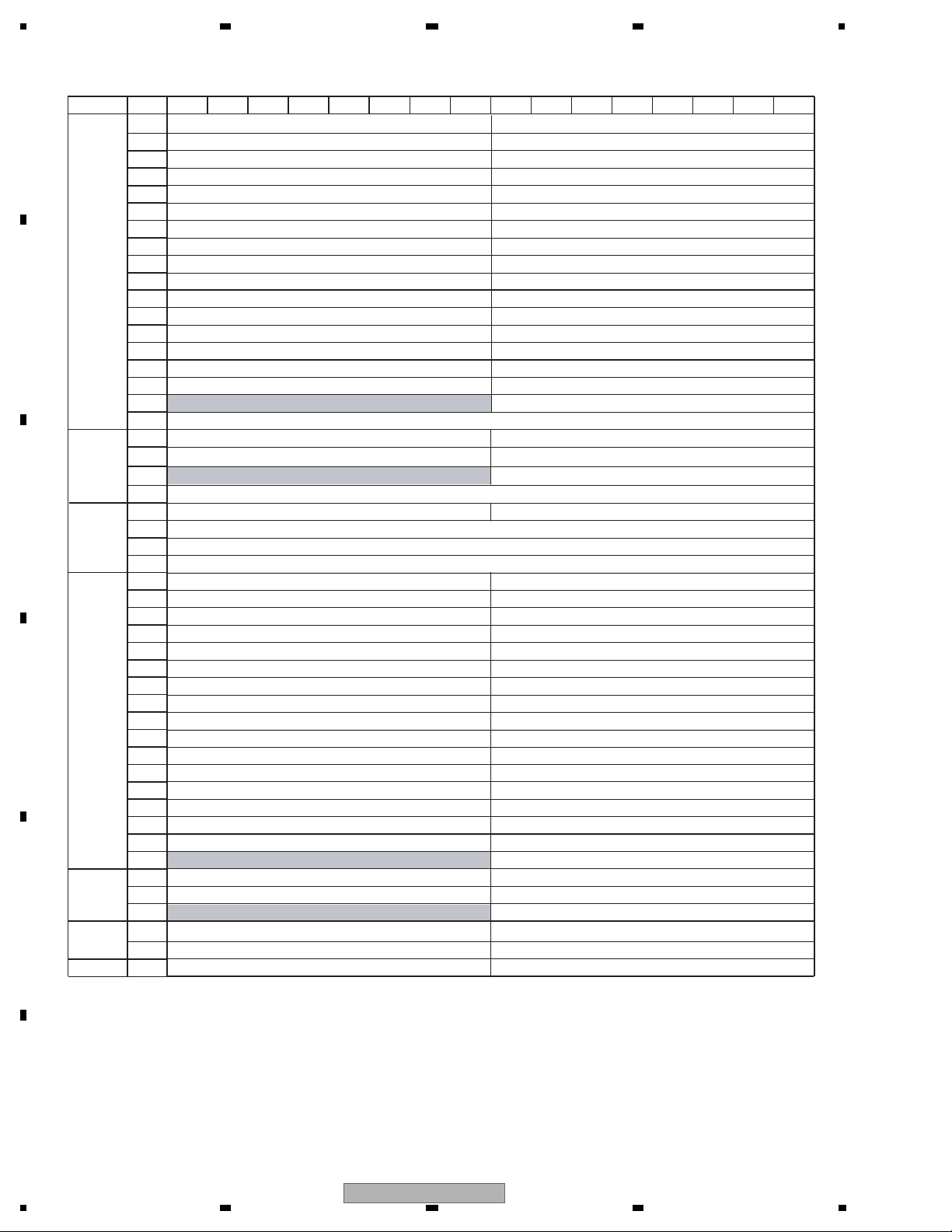
1234
ADDRESS
A
Tou c h
correction value
(Factory
shipment value)
B
Tou c h
outermost
circumference
correction value
(Factory
shipment value)
C
D
E
Tou c h
outermost
circumference
correction value
Tou c h
correction
coordinates
(User calibration
value)
Tou c h
outermost
circumference
value
(User calibration
value)
AD correction
touch
Others
Bit15 Bit14 Bit13 Bit12 Bit11 Bit10 Bit9 Bit8 Bit7 Bit6 Bit5 Bit4 Bit3 Bit2 Bit1 Bit0
34h
35h
36h
37h
38h
39h
3Ah
3Bh
3Ch
3Dh
3Eh
3Fh
40h
41h
42h
43h
44h
45h
46h
47h
48h
49h
4Ah
4Bh
4Ch
4Dh
4Eh
4Fh
50h
51h
52h
53h
54h
55h
56h
57h
58h
59h
5Ah
5Bh
5Ch
5Dh
5Eh
5Fh
60h
61h
62h
63h
64h
Outermost circumference X min coordinate value for correction Outermost circumference Y min coordinate value for correction
Touch panel X coordinate 1 Touch panel Y coordinate 1
Touch panel X coordinate 2 Touch panel Y coordinate 2
Touch panel X coordinate 3 Touch panel Y coordinate 3
Touch panel X coordinate 4 Touch panel Y coordinate 4
Touch panel X coordinate 5 Touch panel Y coordinate 5
Touch panel X coordinate 6 Touch panel Y coordinate 6
Touch panel X coordinate 7 Touch panel Y coordinate 7
Touch panel X coordinate 8 Touch panel Y coordinate 8
Touch panel X coordinate 9 Touch panel Y coordinate 9
Touch panel X coordinate 10 Touch panel Y coordinate 10
Touch panel X coordinate 11 Touch panel Y coordinate 11
Touch panel X coordinate 12 Touch panel Y coordinate 12
Touch panel X coordinate 13 Touch panel Y coordinate 13
Touch panel X coordinate 14 Touch panel Y coordinate 14
Touch panel X coordinate 15 Touch panel Y coordinate 15
Touch panel X coordinate 16 Touch panel Y coordinate 16
Don't care
Checksum
Outermost circumference X min
Outermost circumference X max Outermost circumference Y max
Don't care
Checksum
Outermost circumference X max coordinate value for correction
Outermost circumference Y max coordinate value for correction
Checksum
(USER)Touch panel X coordinate 1 (USER)Touch panel Y coordinate 1
(USER)Touch panel X coordinate 2 (USER)Touch panel Y coordinate 2
(USER)Touch panel X coordinate 3 (USER)Touch panel Y coordinate 3
(USER)Touch panel X coordinate 4 (USER)Touch panel Y coordinate 4
(USER)Touch panel X coordinate 5 (USER)Touch panel Y coordinate 5
(USER)Touch panel X coordinate 6 (USER)Touch panel Y coordinate 6
(USER)Touch panel X coordinate 7 (USER)Touch panel Y coordinate 7
(USER)Touch panel X coordinate 8 (USER)Touch panel Y coordinate 8
(USER)Touch panel X coordinate 9 (USER)Touch panel Y coordinate 9
(USER)Touch panel X coordinate 10 (USER)Touch panel Y coordinate 10
(USER)Touch panel X coordinate 11 (USER)Touch panel Y coordinate 11
(USER)Touch panel X coordinate 12 (USER)Touch panel Y coordinate 12
(USER)Touch panel X coordinate 13 (USER)Touch panel Y coordinate 13
(USER)Touch panel X coordinate 14 (USER)Touch panel Y coordinate 14
(USER)Touch panel X coordinate 15 (USER)Touch panel Y coordinate 15
(USER)Touch panel X coordinate 16 (USER)Touch panel Y coordinate 16
Don't care
(USER)Outermost circumference X min
(USER)Outermost circumference X max
Don't care
Touch AD correction value X coordinates Touch AD correction value Y coordinates
(USER)Touch AD correction value X coordinates (USER)Touch AD correction value Y coordinates
EEPROM completion EJECT lock status value
Touch panel calibration adjustment result
Outermost circumference Y min
Touch panel outermost circumference adjustment result
(USER)Touch panel outermost circumference adjustment result
(USER)Outermost circumference Y min
(USER)Outermost circumference Y max
(USER)Touch panel outermost circumference adjustment result
F
84
1234
AVH-P5900DVD/XN/UC
Page 85
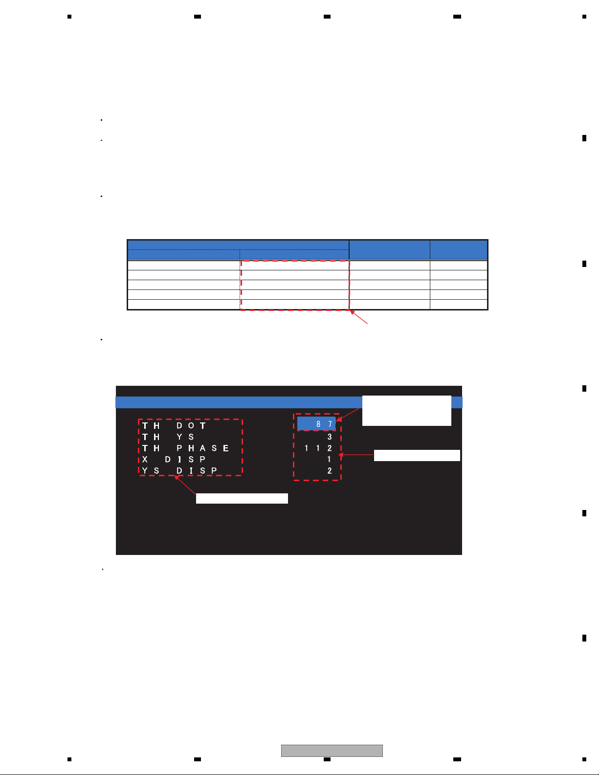
5 678
8.6 MONITOR TEST MODE
[Outline]
It is a mode used to adjust each preset value stored in the EEPROM for storing the preset values.
The adjusted values are stored in the EEPROM for storing the preset values.
[Method for Mode IN]
The method for Mode IN varies depending on the operational environment.
When operated as a unit
Reset the monitor micro computer while the [STEST1] terminal is set to Low and the [EPRTEST] terminal is set to Low.
When operated as a product
Reset the monitor micro computer while the [STEST1] terminal is set to High and the [EPRTEST] terminal is set to Low.
Or, turn the power ON while pressing DISP key and FLIP DOWN key.
[Basic explanation on each menu]
In the "setting content", adjustment range, initial value, and displayed character string of the items preset in each
menu are described.
[Example) Setting content]
Setting item
Content
Displayed character string
Dot search threshold TH DOT 0-255 112
YS search threshold TH YS 0-4 3
Phase search threshold TH PHASE 0-255 112
X disp X DISP 0-63 32
YS disp YS DISP 0-4 2
Adjustment range Initial value
A
B
Character string displayed on the screen.
In the "display specifications", the screen actually displayed under each menu is explained.
Display example is shown below for explanation.
[Example) Display specifications]
< L I N E 3 >
Setting item is displayed.
The item being selected
↓
by ↓ keys is painted
out by the blue cursor.
Display of preset value.
Cursor color
When accessing normally to EEPROM:
The cursor color will change blue
→
red → blue.
(The bule color continues for the convenience of the display cycle.But it is not an error.)
When accessing abnormally to EEPROM(error):
The cursor color will stay red (blue
Note) When a value is changed continuously, the cursor color may change blue
→
red → red) even if the key is released.
→
red → red → ... → blue.
But it is not an error.
(The red color continues for the convenience of the display cycle.)
C
D
E
56
AVH-P5900DVD/XN/UC
F
7
8
85
Page 86
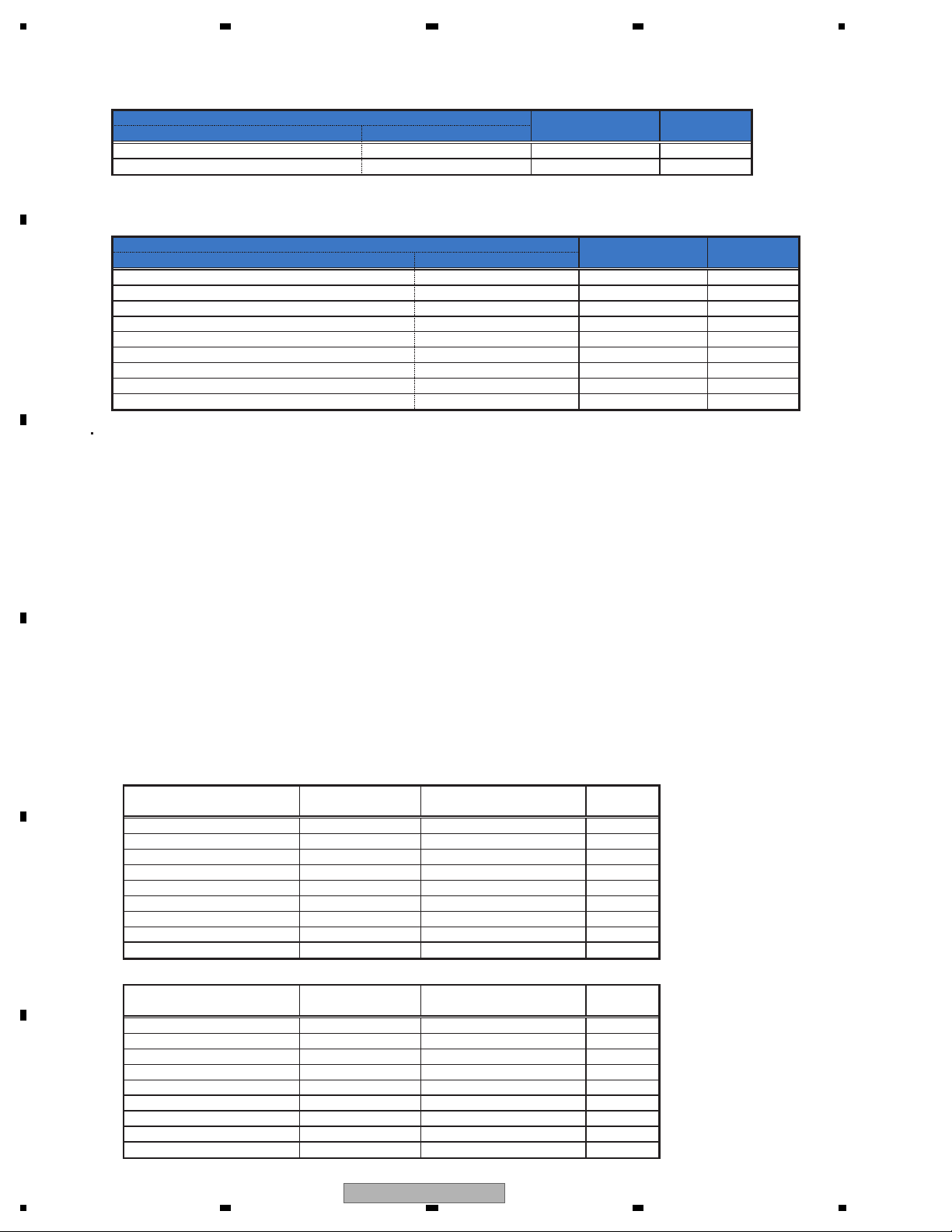
1234
[Flicker adjustment menu]
[Setting content]
A
Content
Setting item
Displayed character string
COM DCCommon inverted output center value 920-255
Adjustment range
Initial value
[Line adjustment 1 menu]
[Setting content]
Setting item
Content
Displayed character string
Bright BRIGHT
RGB simultaneous contrast(SA0C[D7-0])
B
Common inverted output amplitude adjusted value
R output DC offset(SA1A[D11-8])
G output DC offset(SA1C[D11-8])
B output DC offset(SA1E[D11-8])
Main Y contrast(SA0F[D5-0])
CONTRAST
COM AMP AJ
ROUT BIAS
GOUT BIAS
BOUT BIAS
RGB CNTRST
Sub Y contrast(SA13[D5-0]) CMP CNTRST 0-63 26
Dither bit(SA0D[D15]) DITHER BIT 0-1
The bright value is determined by the image quality setting table based on the user setting step and
the common inverted output amplitude adjusted value (COM AMPAJ).
This bright value controls the output of [DACDI] of the monitor micro computer terminal.
Supplement 1)
When the bright value is changed in the test mode, however, it will not be reflected in the user
setting step value.
C
Supplement 2) In the test mode during monitor unit operation, the user setting step will not be reflected in
the bright value calculation.
Adjustment range Initial value
0-255 150
0-255
0-255
0-15
0-15
0-15
0-63
168
150
8
8
8
34
0(OFF)
Note 1... The "black density (=bright)" adjustment by the user is accomplished only by controlling
the common inverted output amplitude, and the brightness of the double window IC is not used.
Note 2... The content of bright and of RGB simultaneous contrast are reference values (adjustable though)
only when adjusting other items, and are not stored in the EEPROM.
Note 3...
Be careful as the content of R(G/B) output DC offset, main Y contrast and sub Y contrast are different
between the displayed values (EEPROM written values) and the register setting values in
the double window IC.
(Because the relationship between the double window IC register value and the screen output
value is not linear, there is a need for conversion by software.)
D
The cases where the displayed value (EEPROM written values) and the register setting values in
the double window IC are different are summarized below.
[R(G/B) output DC offset]
Displayed value (=adjusted value)
(DEC)
15
14 14 0110
:
9 9 0001
8 8 0000 (TYP)
E
77
:
1 1 1001
0 0 1000 (MIN)
[Main Y contrast, sub Y contrast]
Displayed value (=adjusted value)
(DEC)
63 63
62 62 011110
:
33 33 000001
32 32 000000 (TYP)
F
31 31 111111
:
1 1 100001
0 0 100000 (MIN)
EEPROM written value
Double window IC register value
(DEC) (BIN)
15 0111 (MAX)
::
::
E2PROM written value
Double window IC register value
(DEC) (BIN)
:
:
11111
011111 (MAX)
:
:
86
AVH-P5900DVD/XN/UC
1234
Page 87
5 678
[Line adjustment 2 menu]
[Setting content]
Content
RGB & YS horizontal positioning(SA2B[D15-8]) 63
Displayed character string
Setting item
Adjustment range
0-255DOT H POSIT
YS sampling phase 1(SA2D[D15-12]) YS SAMPL 0-15 12
AD sampling phase B(SA2D[D11-8]) B SAMPL 0-15 12
AD sampling phase G(SA2D[D7-4]) G SAMPL 0-15 12
AD sampling phase R(SA2D[D3-0]) R SAMPL 0-15 12
YS internal delay adjustment(SA2F[D3-0]) YS DELAY 0-15 12
Note 1... Be careful as the displayed value (EEPROM written value) and the register setting values in
the double window IC
are different for the following items.
(Because the relationship between the double window IC register value and the screen output
value is not linear, there is a need for conversion by software.)
YS sampling phase 1
AD sampling phase B
AD sampling phase G
AD sampling phase R
YS internal delay adjustment
Initial value
The cases where the displayed value (EEPROM written values) and the register setting values in
the double window IC are different are summarized below.
[YS sampling phase 1, AD sampling phase B/G/R, YS internal delay adjustment]
Displayed value (=adjusted value)
(DEC)
15 15 0111 (MAX)
14 14 0110
:
9 9 0001
8 8 0000 (TYP)
7 7 1111
:::
1 1 1001
0 0 1000 (MIN)
E2PROM written value
Double window IC register value
(DEC) (BIN)
::
A
B
C
[Line adjustment 3 menu]
[Setting content]
Content
Dot search threshold TH DOT 0-255 87
YS search threshold
Phase search threshold TH PHASE 0-255 112
X disp X DISP 0-63 1
YS disp YS DISP 0-4 2
[Line adjustment 4 menu]
[Setting content]
Content
Main horizontal enhancer gain(SA10[D13-12]) M H GAIN 0-3 0
Main horizontal enhancer limiter(SA10[D11-10]) M H LIMIT 0-3 0
Main horizontal enhancer f0(SA10[D8]) M H F0 0-1 0
Main vertical enhancer gain(SA10[D7-6]) M V GAIN 0-3 0
Main vertical enhancer return(SA10[D5-4]) M V ORI 0-3 0
Main vertical enhancer corering(SA10[D3-2]) M V CORE 0-3 0
Setting item
Displayed character string
Setting item
Adjustment range
TH YS 0-4 3
Displayed character string
Adjustment range Initial value
D
Initial value
E
F
56
AVH-P5900DVD/XN/UC
7
8
87
Page 88
1234
[Line adjustment 5 menu]
[Setting content]
A
Content
Sub horizontal enhancer gain(SA10[D13-12]) S H GAIN 0-3 0
Sub horizontal enhancer limiter(SA10[D11-10]) S H LIMIT 0-3 1
Sub horizontal enhancer f0(SA10[D8]) S H F0 0-1 1
Sub vertical enhancer gain(SA10[D7-6]) S V GAIN 0-3 0
Sub vertical enhancer return(SA10[D5-4]) S V ORI 0-3 1
Sub vertical enhancer corering(SA10[D3-2]) S V CORE 0-3 2
Setting item
Displayed character string
Adjustment range
Initial value
[Line adjustment 6 menu]
B
C
[Setting content]
Content
Displayed character string
Brightness R(SA0C[D13-8]) BRIGHT R 0-63 16
Brightness G(SA0D[D13-8]) BRIGHT G 0-63 16
Brightness B(SA0E[D13-8]) BRIGHT B 0-63 16
γ correction ON/OFF(SA1A[D15]) GAMMA OFF
Setting item
RGB simultaneous ? 1 inflection point(SA1A[D5-0])
RGB simultaneous ? 2 inflection point(SA1B[D12-8])
RGB simultaneous ? 3 inflection point(SA1B[D4-0])
RGB simultaneous ? inclination A(SA1A[D14-12])
RGB simultaneous ? inclination B(SA1B[D15-13])
RGB simultaneous ? inclination C(SA1B[D7-5])
GAMMA 1 0-63 0
GAMMA 2 0-31 4
GAMMA 3 0-31 1
GAMMASLP A 0-7 4
GAMMASLP B 0-7 1
GAMMASLP C
Note 1... Be careful as the displayed value (EEPROM written value) and the register setting values in
the double window IC
are different for the following items.
(Because the relationship between the double window IC register value and the screen output
value is not linear, there is a need for conversion by software.)
Brightness R
Brightness G
Brightness B
Adjustment range Initial value
0-7 1
The cases where the displayed value (EEPROM written values) and the register setting values in
the double window IC are different are summarized below.
D
E
[Brightness R/G/B]
Displayed value (=adjusted value)
(DEC)
63 63
62 62 011110
:::
33
32 32 000000 (TYP)
31 31
:::
1 1 100001
0 0 100000 (MIN)
E2PROM written value
Double window IC register value
(DEC) (BIN)
33 000001
011111 (MAX)
111111
[Line adjustment 7 menu]
[Setting content]
Content
Displayed character string
Main PLL0(SA24[D15-8])
Setting item
Main PLL1(SA24[D7-0])
Main PLL2(SA25[D15-8])
Main PLL3(SA25[D7-0])
F
MAIN PLL1 0-255 13
MAIN PLL2 0-255 204
MAIN PLL3 0-255 4
Adjustment range
0-255MAIN PLL0
Initial value
158
88
AVH-P5900DVD/XN/UC
1234
Page 89
5 678
[Line adjustment 8 menu]
[Setting content]
Content
During TV, sub PLL0(SA26[D15-8])
During TV, sub PLL1(SA26[D7-0])
Other, sub PLL0(SA27[D15-8])
Other, sub PLL1(SA27[D7-0])
During TV, sub PLL2(SA28[D15-8])
During TV, sub PLL3(SA28[D7-0])
Other, sub PLL2(SA29[D15-8])
Other, sub PLL3(SA29[D7-0])
[Line adjustment 9 menu]
[Setting content]
Content
SA46[D15-8]
SA46[D7-0]
SA47[D15-8]
SA47[D7-0]
SA48[D15-8]
SA48[D7-0]
SA49[D15-8]
SA49[D7-0]
SA4A[D15-8]
SA4A[D7-0]
Setting item
Setting item
Displayed character string
Displayed character string
SUB PLL0 TV
SUB PLL1 TV
SUB PLL0
SUB PLL1
SUB PLL2 TV
SUB PLL3 TV
SUB PLL2
SUB PLL3
Adjustment range Initial value
0-255 140
0-255 136
0-255 140
0-255 141
0-255 100
0-255 68
0-255 152
0-255 107
Adjustment range Initial value
SA46H UPPER 0-255 2
SA46H LOWER 0-255 0
SA47H UPPER 0-255 0
SA47H LOWER 0-255 0
SA48H UPPER 0-255 0
SA48H LOWER 0-255 0
SA49H UPPER 0-255 0
SA49H LOWER 0-255 0
SA4AH UPPER 0-255 0
SA4AH LOWER 0-255 0
A
B
C
[Line adjustment 10 menu]
[Setting content]
Content
SA4B[D15-8]
SA4B[D7-0]
SA4C[D15-8]
SA4C[D7-0]
SA4D[D15-8]
SA4D[D7-0]
SA4E[D15-8]
SA4E[D7-0]
SA4F[D15-8]
SA4F[D7-0]
Setting item
Displayed character string
Adjustment range Initial value
SA4BH UPPER 0-255 0
SA4BH LOWER 0-255 0
SA4CH UPPER 0-255 0
SA4CH LOWER 0-255 0
SA4DH UPPER 0-255 0
SA4DH LOWER 0-255 0
SA4EH UPPER 0-255 0
SA4EH LOWER 0-255 0
SA4FH UPPER 0-255 0
SA4FH LOWER 0-255 0
D
E
56
AVH-P5900DVD/XN/UC
F
7
8
89
Page 90
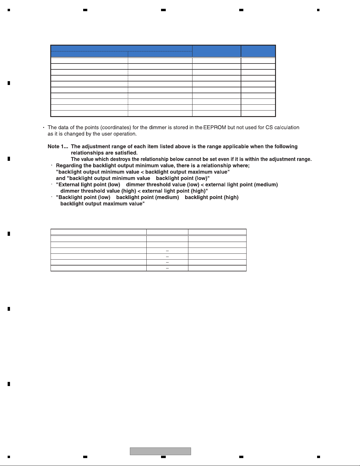
1234
[Dimmer parameter setting menu]
[Setting content]
A
Content Displayed character string
Backlight output max value BL MAX 0x00-0xFF C4
Backlight output min value BL MIN 0x00-0xFE 59
Dimmer threshold value (high) REF H 0x01-0xFE C0
Dimmer threshold value (low) REF L 0x00-0xFD 60
External light point (high) LUM H 0x02-0xFF E2
External light point (medium) LUM M 0x01-0xFE 87
External light point (low) LUM L 0x00-0xFD 52
Backlight point (high) BL H 0x00-0xFF C4
Backlight point (medium) BL M 0x00-0xFF C4
Backlight point (low) BL L 0x00-0xFF 68
B
<
C
=
<
=
Setting item
<
=
<
=
Adjustment range Initial value
<
=
<
=
<
=
<
=
[Operational specifications]
Operational description Main unit key Remote controller key
Main page select -
Main page select +
Selection cursor upward movement
Selection cursor downward movement
Item content adjustment
D
E
Item content adjustment
PGM(TA) BAND/ESC
DISP BACK
←
↓
↓
→
F
90
1234
AVH-P5900DVD/XN/UC
Page 91
5 678
8.7 CALIBRATION TEST
[Mode IN method]
After pressing [PGM(TA)+OPEN/CLOSE], press RESET and START. Then the screen will change to
[touch panel adjustment mode].
[Menu types for mode]
Calibration test mode consists of the following menu.
(By clicking each menu, you can read the explanation for each menu.)
TOP menu
Outermost circumference Inspection
16 points adjustment
Coordinate inspection
Calibration verification
Data initialization
0. Explanation of the TOP menu
[Operational specifications]
Operational
description
Menu
Remote controller
key
MENU_ENTER
determination
Selection cursor
up movement
Selection cursor
down movement
A
B
C
Select the menu desired to be adjusted using the up/down key ( ), then press ENTER key to enter
into the selected menu.
Note 1) Calibration menu can be selected only when adjustment of the outermost circumference has been
completed normally.
[Display specifications]
Adjustment completed mark
[ U P , D O W N
] : C u r s o r m o v e m e n t
Flicker initialized state
[ A . M E N U ] : M e n u s e l e c t i o n
[ A C C O F F ] : E n d o f t e s t
D
E
Operational specifications are displayed
AVH-P5900DVD/XN/UC
56
F
7
8
91
Page 92
1234
Conditions for lighting of the adjustment complete mark “ ”.
A
Outermost circumference inspection :
In case the outermost circumference inspection has been completed normally.
16 points adjustment :
In case the calibration has been completed normally.
Conditions for the adjustment complete mark “ ” to go out
Outermost circumference inspection :
In case the outermost circumference inspection has never been performed.
In case the EEPROM initialization has been performed.
In case the adjustment value has been initialized.
B
16 points adjustment :
In case the 16 points adjustment has never been performed.
In case the EEPROM initialization has been performed.
In case the adjustment value has been initialized.
1. Set up TP effective range
[Outline]
C
panel screen.
When exiting the menu screen by pressing ENTER key, the captured value is stored in the EEPROM.
Furthermore, when storing the value, checking is made as to whether the value is within the range or not.
If the value is within the range, OK is displayed, and X/Y upper and lower limit value and normal ending information,
total of 5 byte data, are written in the EEPROM. (In or out of the range check is conducted according to the
[Table of allowable range of setting value] shown below.)
In the following cases, however, NG will be displayed without storing the EEPROM captured value.
When the set value is outside of the range. (When the value exceeded the [Table of allowable range of setting
value] below.)
Outermost circumference value of X and Y is obtained by tracing the outermost circumference of the touch
D
However, "adjustment NG information" (1 byte) is written into the EEPROM.
When writing into the EEPROM failed.
The transition of the state for the above described outermost circumference inspection is outlined below.
OK (normal ending)
Outermost
circumference
inspection in
process
E
Outermost circumference
inspection completed
EEPROM writing
in process
Adjustment error
EEPROM writing error
Press ENTER key
TOP menu
F
92
1234
AVH-P5900DVD/XN/UC
Page 93
5 678
Refer to the "Memory item list and EEPROM" for the stored area of the setting value in the EEPROM. Initial value and
setting value allowable range are as shown below.
[Table of BEFORE initial value]
Coordinate Minimum value Maximum value
X 43 247
Y 50 238
[Table of setting value allowable range]
Coordinate Minimum value Maximum value
X 0~72 205~255
Y 0~80 205~255
[Display specifications]
Outermost circumference inspection in process
[Table of AFTER initial value]
Coordinate Minimum value Maximum value
X 90 180
Y 90 180
A
B
C
[ A . M E N U ] :
X/Y information of [MIN] and [MAX] of the outermost circumference are displayed.
[BEFOR] indicates the value stored in the EEPROM.
[AFTER] indicates MIN/MAX of the A/D value currently captured.
When ended normally.
[ A . M E N U ]
D
E
56
AVH-P5900DVD/XN/UC
F
7
8
93
Page 94
1234
The data written are as follows.
Upper limit value and lower limit value of X.
Upper limit value and lower limit value of Y.
A
Adjustment OK information.
When the captured value is outside of the allowable range.
B
[ A . M E N U ]
C
Adjustment NG information.
[Key operation specifications]
The data written is as follows.
Operational
description
Remote controller
key
To TOP menu MENU_ENTER
2. Set up calibration
D
[Outline]
Touch the cursor [+] displayed on the screen. When correctly touched, the cursor will disappear, and the next
cursor will appear. Calibration is conducted by repeating this process 16 times. When the 17th point has been
finally touched, setting information for the 16 points and the normal ending information, total of 17 byte data,
are written into the EEPROM, and the screen returns to the TOP menu.
In the following cases, however, NG will be displayed without storing the EEPROM captured value.
When the menu is exited before touching the 17th point.
However, ’adjustment NG information’ (1 byte) is written into the EEPROM.
When writing into the EEPROM failed.
E
The transition of the state for the above described 16 points adjustment is outlined below.
OK (normal ending)
16 points
adjustment in
process
16 points adjustment
completed
F
94
1234
EEPROM writing
in process
AVH-P5900DVD/XN/UC
Adjustment error
EEPROM writing error
Press ENTER key
TOP menu
Page 95

5 678
Refer to the material titled [Memory item list and EEPROM] for the stored area of the setting value in the EEPROM.
[Display specifications]
A
16 points adjustment in process
B
C
When ended normally.
[ A . M E N U ]
The data written are as follows.
X coordinate (16 points)
Y coordinate (16 points)
[Key operation specifications]
Operational
description
To TOP menu MENU_ENTER
D
E
Remote controller
key
F
56
AVH-P5900DVD/XN/UC
7
8
95
Page 96
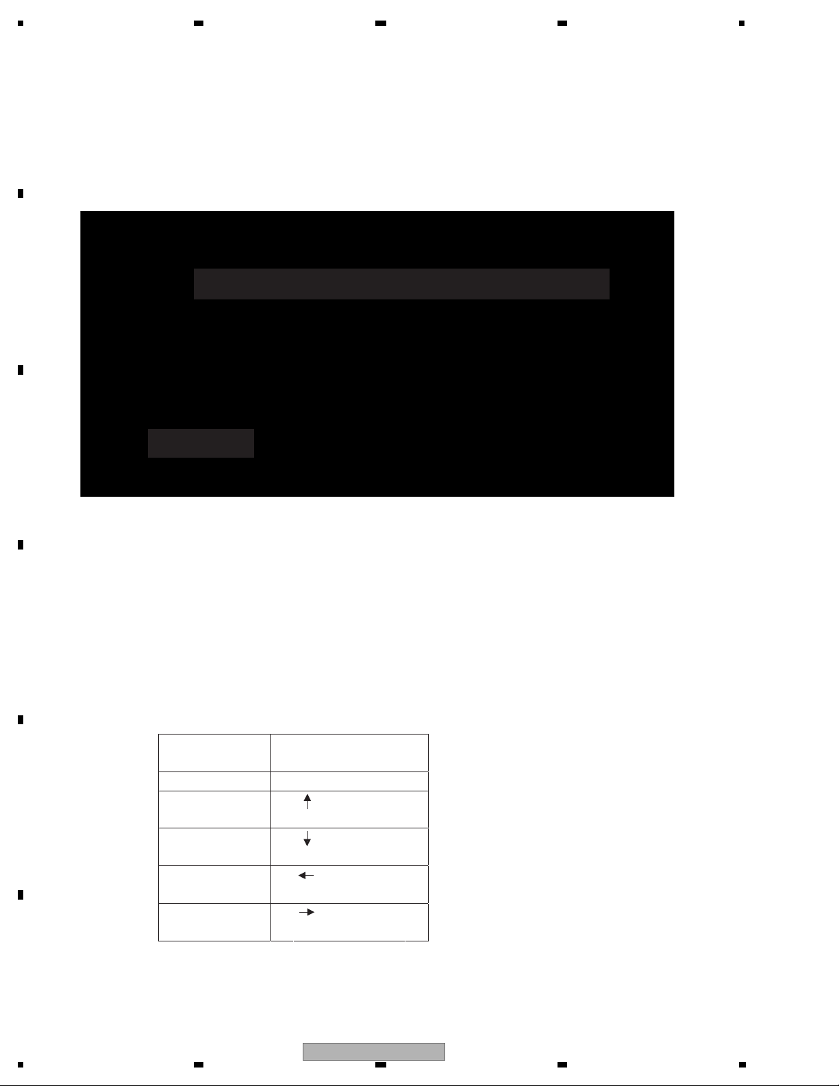
1234
3. TP coordinates test
[Outline]
A
Coordinate before and after the correction when the touch panel is touched is displayed, and the operation is verified.
Furthermore, the cursor can be moved by using the up/down/left/right keys, and the coordinate of the cursor center
is displayed.
The cursor is displayed in red at the positions where the cursor was displayed during 16 points adjustment.
[Display specifications]
B
Display is
made in HEX.
C
AD : AD data value (X direction, Y direction), representing the coordinate of the point pressed, is displayed.
VD E2P : VD value (the value registered at the time of circumference setting) preset in the EEPROM.
VD : VD value currently being pressed.
NORMAL : The coordinate (X direction, Y direction), which is the result of normalizing the AD data value currently
being pressed within the effective range, is displayed.
[ A . M E N U ]
D
CALIBRATION : The coordinate (X direction, Y direction), which is the result of applying the correction by calibration
to the normalized coordinate, is displayed.
[Key operation specifications]
Operational
description
Remote controller
key
To TOP menu MENU_ENTER
E
Cursor upward
movement
Cursor downward
movement
Cursor leftward
movement
Cursor rightward
movement
F
96
1234
AVH-P5900DVD/XN/UC
Page 97

5 678
[Calibration verification]
[Outline]
■ Touch the center of the "+" cursor displayed on the screen. When touched correctly, the cursor will disappear,
and the next cursor will be displayed.
By repeating this 16 times, corrected value for each "+" point is obtained.
The information are written into the EEPROM as a data of 16 times. The screen will return to the top menu.
[Display specifications]
"+" changes into red when coordinates to touch are outside the range.
A
B
C
■
When terminated normally. (After pressing the 16th point.)
[Key operation specifications]
Operational description Remote controller key
To top menu MENU_ENTER
D
E
56
AVH-P5900DVD/XN/UC
F
7
8
97
Page 98
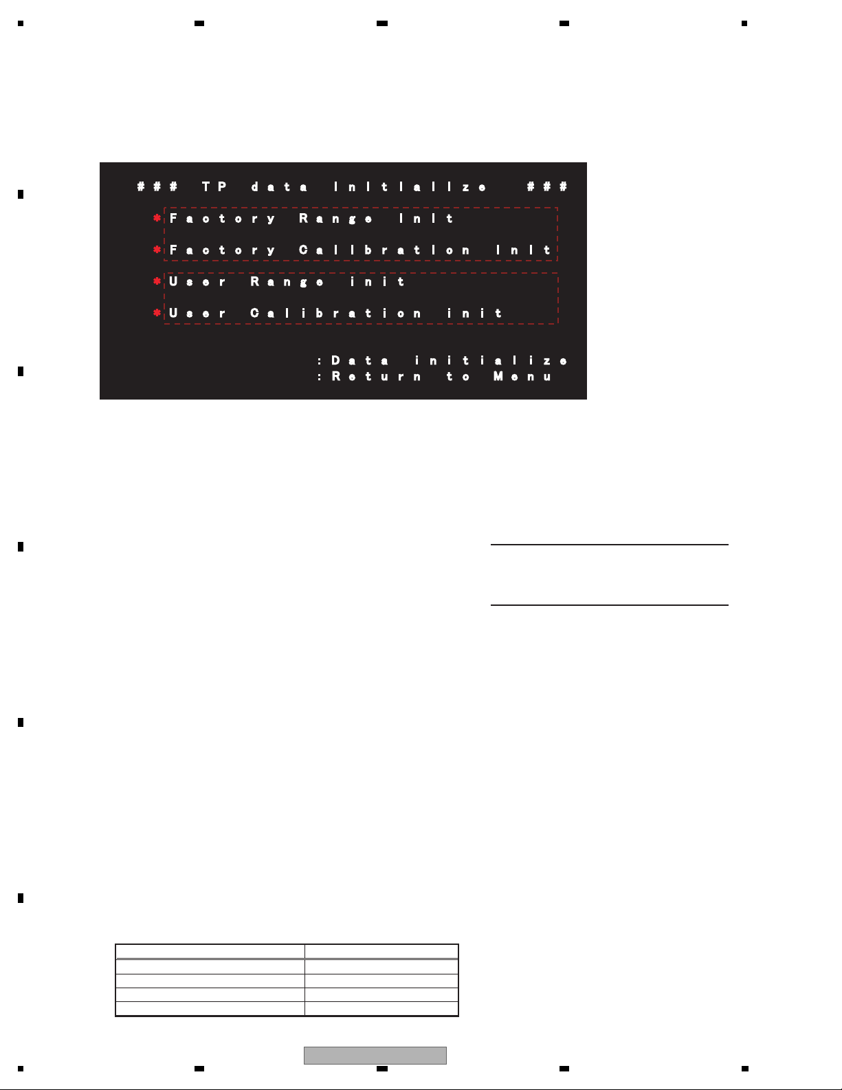
1234
■
■
■
■
■
■
■
■
[Data initialization]
[Outline]
■ Result of outermost circumference inspection and of calibration inspection (corrected value) are returned to
A
their initial values.
As for the initialized items, the initial values are written into the EEPROM and the adjustment information is cleared.
[Display specifications]
B
[B A C K ]
[A. M E N E ]
■ Conditions for the adjustment completion mark (*) to be lighted up.
(The mark will be lighted up if one of the multiple conditions is met.)
C
When the outermost circumference inspection of the calibration for line has been completed normally.
When the calibration inspection for line has been completed normally.
When the outermost circumference inspection of calibration for line has been completed normally.
When the outermost circumference inspection of the user calibration has been completed normally.
When the calibration inspection for line has been completed normally.
When the calibration inspection of the user calibration has been completed normally.
D
(The mark will go out if one of the multiple conditions is met.)
When the above mentioned lighting conditions are not applicable.
When the adjusted value has been initialized (Data initialize).
When the EEPROM has been initialized.
When the above mentioned lighting conditions are not applicable.
When the adjusted value has been initialized (Data initialize).
When the EEPROM has been initialized.
When the above mentioned lighting conditions are not applicable.
E
When the adjusted value has been initialized (Data initialize).
When the EEPROM has been initialized.
When the above mentioned lighting conditions are not applicable.
When the adjusted value has been initialized (Data initialize).
When the EEPROM has been initialized.
Outermost circumference inspection
16 point adjustment
User outermost circumference inspection
(Because the writing is made to both the Factory region and the User region, the user side will also be treated as adjusted.)
User 16 point adjustment
(Because the writing is made to both the Factory region and the User region, the user side will also be treated as adjusted.)
■ Conditions for the adjustment completion mark (*) to go out.
Outermost circumference inspection
16 point adjustment
User outermost circumference inspection
User 16 point adjustment
[Key operation specifications]
Operational description Remote controller key
Determination of initializing item BACK
F
Selected cursor up movement
Selected cursor down movement ↓
To top menu MENU_ENTER
98
1234
AVH-P5900DVD/XN/UC
↓
Page 99

5 678
A
B
C
D
E
56
AVH-P5900DVD/XN/UC
F
7
8
99
Page 100
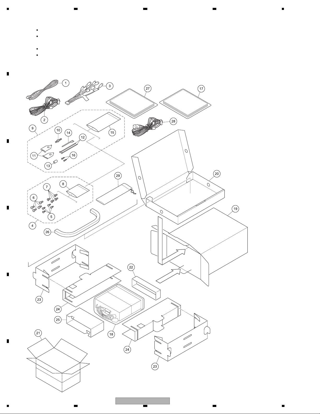
1234
N
9. EXPLODED VIEWS AND PARTS LIST
OTES : Parts marked by " * " are generally unavailable because they are not in our Master Spare Parts List.
The > mark found on some component parts indicates the importance of the safety factor of the part.
A
Therefore, when replacing, be sure to use parts of identical designation.
Screw adjacent to mark on the product are used for disassembly.
For the applying amount of lubricants or glue, follow the instructions in this manual.
(In the case of no amount instructions,apply as you think it appropriate.)
9.1 PACKING
B
""
C
D
E
F
100
1234
AVH-P5900DVD/XN/UC
 Loading...