

Philips PCA8581CT-F6, PCA8581T-F6, PCA8581T-F6L, PCF8581CT-F4 Datasheet

DATA SH EET
Product specification
Supersedes data of 1996 Aug 19
File under Integrated Circuits, IC12
1997 Apr 02
INTEGRATED CIRCUITS
PCA8581; PCA8581C
128 × 8-bit EEPROM with I
2
C-bus
interface

1997 Apr 02 2
Philips Semiconductors Product specification
128 × 8-bit EEPROM with I2C-bus interface
PCA8581; PCA8581C
CONTENTS
1 FEATURES
2 GENERAL DESCRIPTION
3 QUICK REFERENCE DATA
4 ORDERING INFORMATION
5 BLOCK DIAGRAM
6 PINNING
7 CHARACTERISTICS OF THE I2C-BUS
7.1 Bit transfer
7.2 Start and stop conditions
7.3 System configuration
7.4 Acknowledge
7.5 I2C-bus protocol
8 LIMITING VALUES
9 HANDLING
10 DC CHARACTERISTICS
11 AC CHARACTERISTICS
12 APPLICATION INFORMATION
12.2 Application example
12.2 Slave address
12.3 Diode protection
13 PACKAGE OUTLINES
14 SOLDERING
14.1 Introduction
14.2 DIP
14.2.1 Soldering by dipping or by wave
14.2.2 Repairing soldered joints
14.3 SO
14.3.1 Reflow soldering
14.3.2 Wave soldering
14.3.3 Repairing soldered joints
15 DEFINITIONS
16 LIFE SUPPORT APPLICATIONS
17 PURCHASE OF PHILIPS I2C COMPONENTS

1997 Apr 02 3
Philips Semiconductors Product specification
128 × 8-bit EEPROM with I2C-bus interface
PCA8581; PCA8581C
1 FEATURES
• Operating supply voltage:
– 4.5 to 5.5 V (PCA8581)
– 2.5 to 6.0 V (PCA8581C)
• Integrated voltage multiplier and timer for writing
(no external components required)
• Automatic erase before write
• Low standby current; maximum 10 µA
• 8-byte page write mode
• Serial input/output bus (I2C-bus)
• Address by 3 hardware address pins
• Automatic word address incrementing
• Designed for minimum 10000 write cycles per byte
• 10 years minimum non-volatile data retention
• Infinite number of read cycles
• Pin and address compatibility to PCF8570C and
PCF8582
• Operating ambient temperature: −25 to +85 °C.
2 GENERAL DESCRIPTION
The PCA8581 and PCA8581C are low power CMOS
EEPROMs with standard and wide operating voltages:
4.5 to 5.5 V (PCA8581)
2.5 to 6.0 V (PCA8581C).
In the following text, the generic term ‘PCA8581’ is used to
refer to both types in all packages except when otherwise
specified.
The PCA8581 is organized as 128 words of 8-bytes.
Addresses and data are transferred serially via a two-line
bidirectional bus (I2C-bus). The built-in word address
register is incremented automatically after each written or
read data byte. All bytes can be read in a single operation.
Up to 8 bytes can be written in one operation, reducing the
total write time per byte. Three address pins, A0, A1 and
A2 are used to define the hardware address, allowing the
use of up to 8 devices connected to the bus without
additional hardware.
3 QUICK REFERENCE DATA
4 ORDERING INFORMATION
SYMBOL PARAMETER CONDITIONS MIN. MAX. UNIT
V
DD
supply voltage
PCA8581 4.5 5.5 V
PCA8581C 2.5 6.0 V
I
DD
supply current (standby) f
SCL
= 0 Hz − 10 µA
T
amb
operating ambient temperature −25 +85 °C
T
stg
storage temperature without EEPROM retention −65 +150 °C
with EEPROM retention −65 +85 °C
TYPE
NUMBER
PACKAGE
NAME DESCRIPTION VERSION
PCA8581P DIP8 plastic dual in-line package; 8 leads (300 mil) SOT97-1
PCA8581CP DIP8 plastic dual in-line package; 8 leads (300 mil) SOT97-1
PCA8581T SO8 plastic small outline package; 8 leads; body width 3.9 mm SOT96-1
PCA8581CT SO8 plastic small outline package; 8 leads; body width 3.9 mm SOT96-1
1997 Apr 02 4
Philips Semiconductors Product specification
128 × 8-bit EEPROM with I2C-bus interface
PCA8581; PCA8581C
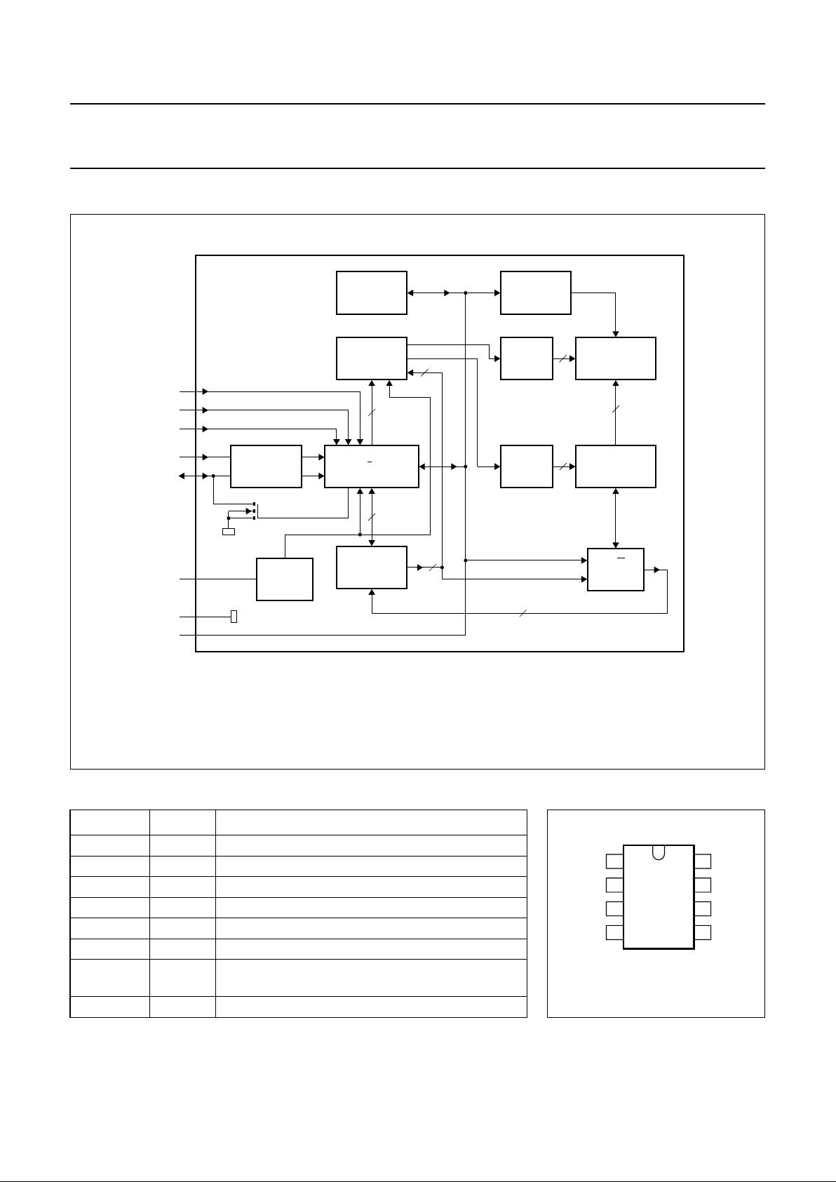
5 BLOCK DIAGRAM
Fig.1 Block diagram.
handbook, full pagewidth
MLB887
TIMER
WORD
ADDRESS
REGISTER
SHIFT
REGISTER
POWER
ON
RESET
INPUT
FILTER
VOLTAGE
MULTIPLIER
ROW
SELECT
MEMORY
CELL
ARRAY
COLUMN
SELECT
MULTIPLEXER
R/W
CONTROL
I C BUS
CONTROL
2
6
5
SCL
SDA
3
A2
2
A1
1
A0
8
V
DD
4
V
SS
7
TEST
PCA8581
PCA8581C
7
8
6 PINNING
SYMBOL PIN DESCRIPTION
A0 1 hardware address input 0
A1 2 hardware address input 1
A2 3 hardware address input 2
V
SS
4 negative supply
SDA 5 serial data input/output
SCL 6 serial clock input
TEST 7 test output can be connected to V
SS
, VDD or left
open-circuit
V
DD
8 positive supply
Fig.2 Pin configuration.
page
1
2
3
4
8
7
6
5
MLB888
PCA8581
PCA8581C
SCL
SDA
A2
A1
A0
V
DD
V
SS
TEST

1997 Apr 02 5
Philips Semiconductors Product specification
128 × 8-bit EEPROM with I2C-bus interface
PCA8581; PCA8581C
7 CHARACTERISTICS OF THE I2C-BUS
The I2C-bus is for bidirectional, two-line communication
between different ICs or modules. The two lines are a
serial data line (SDA) and a serial clock line (SCL). Both
lines must be connected to a positive supply via a pull-up
resistor. Data transfer may be initiated only when the bus
is not busy.
7.1 Bit transfer
One data bit is transferred during each clock pulse.
The data on the SDA line must remain stable during the
HIGH period of the clock pulse as changes in the data line
at this time will be interpreted as a control signal.
Fig.3 Bit transfer.
MBA607
data line
stable;
data valid
change
of data
allowed
SDA
SCL
7.2 Start and stop conditions
Both data and clock lines remain HIGH when the bus is not busy. A HIGH-to-LOW transition of the data line, while the
clock is HIGH is defined as the start condition (S). A LOW-to-HIGH transition of the data line while the clock is HIGH is
defined as the stop condition (P).
Fig.4 Definition of START and STOP conditions.
MBA608
SDA
SCL
P
STOP condition
SDA
SCL
S
START condition

1997 Apr 02 6
Philips Semiconductors Product specification
128 × 8-bit EEPROM with I2C-bus interface
PCA8581; PCA8581C
7.3 System configuration
A device generating a message is a ‘transmitter’, a device receiving a message is the ‘receiver’. The device that controls
the message is the ‘master’ and the devices which are controlled by the master are the ‘slaves’.
Fig.5 System configuration.
MBA605
MASTER
TRANSMITTER /
RECEIVER
SLAVE
RECEIVER
SLAVE
TRANSMITTER /
RECEIVER
MASTER
TRANSMITTER
MASTER
TRANSMITTER /
RECEIVER
SDA
SCL
7.4 Acknowledge
The number of data bytes transferred between the start
and stop conditions from transmitter to receiver is
unlimited. Each byte of eight bits is followed by an
acknowledge bit. The acknowledge bit is a HIGH level
signal put on the bus by the transmitter during which time
the master generates an extra acknowledge related clock
pulse. A slave receiver which is addressed must generate
an acknowledge after the reception of each byte. Also a
master receiver must generate an acknowledge after the
reception of each byte that has been clocked out of the
slave transmitter.
The device that acknowledges must pull down the SDA
line during the acknowledge clock pulse, so that the SDA
line is stable LOW during the HIGH period of the
acknowledge related clock pulse (set-up and hold times
must be taken into consideration). A master receiver must
signal an end of data to the transmitter by not generating
an acknowledge on the last byte that has been clocked out
of the slave. In this event the transmitter must leave the
data line HIGH to enable the master to generate a stop
condition.
Fig.6 Acknowledgement on the I2C-bus.
handbook, full pagewidth
MBA606 - 1
START
condition
S
SCL FROM
MASTER
DATA OUTPUT
BY TRANSMITTER
DATA OUTPUT
BY RECEIVER
clock pulse for
acknowledgement
1
2
8
9
 Loading...