

Philips PCF8570P-F5, PCF8570T-F5, PCF8570U-10 Datasheet

DATA SH EET
Product specification
Supersedes data of 1997 Sep 02
File under Integrated Circuits, IC12
1999 Jan 06
INTEGRATED CIRCUITS
PCF8570
256 × 8-bit static low-voltage RAM
with I
2
C-bus interface

1999 Jan 06 2
Philips Semiconductors Product specification
256 × 8-bit static low-voltage RAM with
I
2
C-bus interface
PCF8570
CONTENTS
1 FEATURES
2 APPLICATIONS
3 GENERAL DESCRIPTION
4 QUICK REFERENCE DATA
5 ORDERING INFORMATION
6 BLOCK DIAGRAM
7 PINNING
8 CHARACTERISTICS OF THE I2C-BUS
8.1 Bit transfer
8.2 Start and stop conditions
8.3 System configuration
8.4 Acknowledge
8.5 I2C-bus protocol
9 LIMITING VALUES
10 HANDLING
11 DC CHARACTERISTICS
12 AC CHARACTERISTICS
13 APPLICATION INFORMATION
13.1 Application example
13.2 Slave address
13.3 Power-saving mode
14 PACKAGE OUTLINES
15 SOLDERING
15.1 Introduction
15.2 Through-hole mount packages
15.2.1 Soldering by dipping or by solder wave
15.2.2 Manual soldering
15.3 Surface mount packages
15.3.1 Reflow soldering
15.3.2 Wave soldering
15.3.3 Manual soldering
15.4 Suitability of IC packages for wave, reflow and
dipping soldering methods
16 DEFINITIONS
17 LIFE SUPPORT APPLICATIONS
18 PURCHASE OF PHILIPS I2C COMPONENTS
1999 Jan 06 3
Philips Semiconductors Product specification
256 × 8-bit static low-voltage RAM with
I
2
C-bus interface
PCF8570
1 FEATURES
• Operating supply voltage 2.5 to 6.0 V
• Low data retention voltage; minimum 1.0 V
• Low standby current; maximum 15 µA
• Power-saving mode; typical 50 nA
• Serial input/output bus (I2C-bus)
• Address by 3 hardware address pins
• Automatic word address incrementing
• Available in DIP8 and SO8 packages.
2 APPLICATIONS
• Telephony:
– RAM expansion for stored numbers in repertory
dialling (e.g. PCD33xxA applications)
• General purpose RAM for applications requiring
extremely low current and low-voltage RAM retention,
such as battery or capacitor-backed.
• Radio, television and video cassette recorder:
– channel presets
• General purpose:
– RAM expansion for the microcontroller families
PCD33xxA, PCF84CxxxA, P80CLxxx and most other
microcontrollers.
3 GENERAL DESCRIPTION
The PCF8570 is a low power static CMOS RAM,
organized as 256 words by 8-bits.
Addresses and data are transferred serially via a two-line
bidirectional bus (I2C-bus). The built-in word address
register is incremented automatically after each written or
read data byte. Three address pins, A0, A1 and A2 are
used to define the hardware address, allowing the use of
up to 8 devices connected to the bus without additional
hardware.
4 QUICK REFERENCE DATA
5 ORDERING INFORMATION
SYMBOL PARAMETER CONDITIONS MIN. MAX. UNIT
V
DD
supply voltage 2.5 6.0
I
DD
supply current (standby) f
SCL
=0Hz − 15 µA
I
DDR
supply current (power-saving mode) T
amb
=25°C − 400 nA
T
amb
operating ambient temperature −40 +85 °C
T
stg
storage temperature −65 +150 °C
TYPE
NUMBER
PACKAGE
NAME DESCRIPTION VERSION
PCF8570P DIP8 plastic dual in-line package; 8 leads (300 mil) SOT97-1
PCF8570T SO8 plastic small outline package; 8 leads; body width 7.5 mm SOT176-1

1999 Jan 06 4
Philips Semiconductors Product specification
256 × 8-bit static low-voltage RAM with
I
2
C-bus interface
PCF8570
6 BLOCK DIAGRAM
Fig.1 Block diagram.
handbook, full pagewidth
MLB928
WORD
ADDRESS
REGISTER
SHIFT
REGISTER
POWER
ON
RESET
INPUT
FILTER
ROW
SELECT
MEMORY
CELL
ARRAY
COLUMN
SELECT
MULTIPLEXER
R/W
CONTROL
I C BUS
CONTROL
2
6
5
SCL
SDA
3
A2
2
A1
1
A0
8
V
DD
4
V
SS
7
TEST
PCF8570
7
8
7 PINNING
SYMBOL PIN DESCRIPTION
A0 1 hardware address input 0
A1 2 hardware address input 1
A2 3 hardware address input 2
V
SS
4 negative supply
SDA 5 serial data input/output
SCL 6 serial clock input
TEST 7 Input for power-saving mode (see section
“Power-saving mode”). Also used as a test output
during manufacture. TEST should be tied to V
SS
during normal operation.
V
DD
8 positive supply
Fig.2 Pin configuration.
age
1
2
3
4
8
7
6
5
MLB929
PCF8570
SCL
SDA
A2
A1
A0
V
DD
V
SS
TEST
1999 Jan 06 5
Philips Semiconductors Product specification
256 × 8-bit static low-voltage RAM with
I
2
C-bus interface
PCF8570
8 CHARACTERISTICS OF THE I2C-BUS
The I2C-bus is for bidirectional, two-line communication
between different ICs or modules. The two lines are a
serial data line (SDA) and a serial clock line (SCL). Both
lines must be connected to a positive supply via a pull-up
resistor. Data transfer may be initiated only when the bus
is not busy.
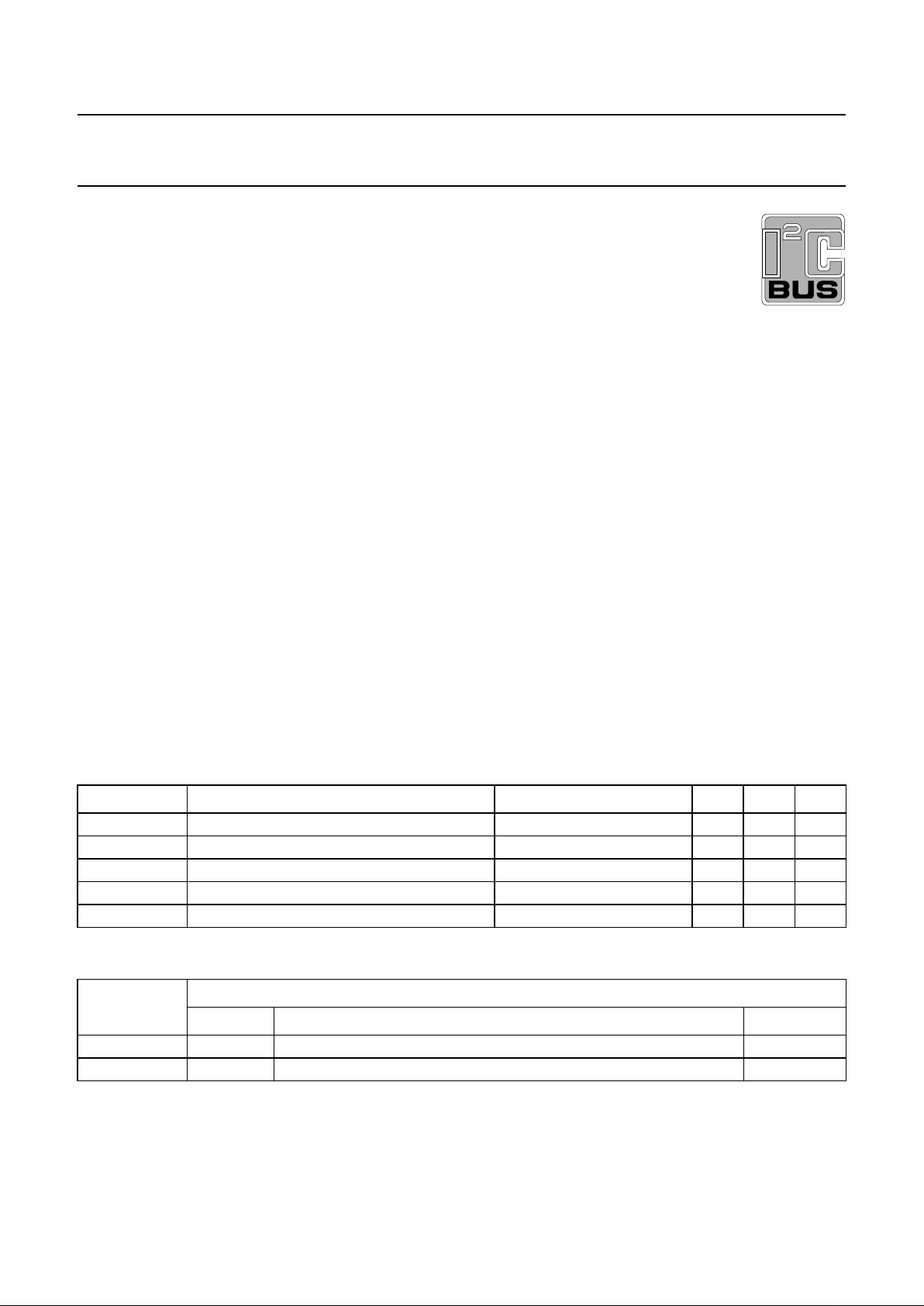
8.1 Bit transfer
One data bit is transferred during each clock pulse.
The data on the SDA line must remain stable during the
HIGH period of the clock pulse as changes in the data line
at this time will be interpreted as a control signal.
Fig.3 Bit transfer.
MBA607
data line
stable;
data valid
change
of data
allowed
SDA
SCL
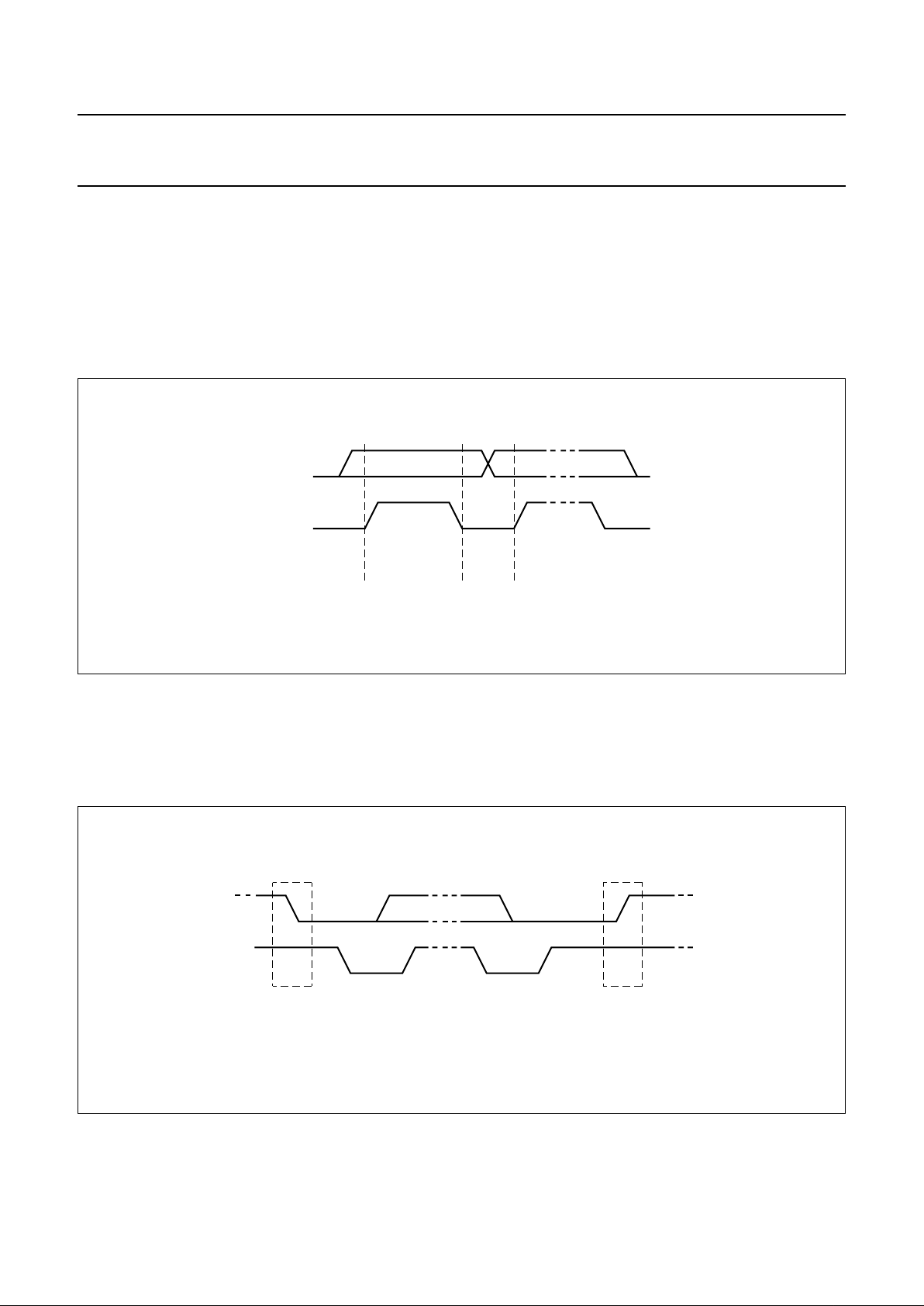
8.2 Start and stop conditions
Both data and clock lines remain HIGH when the bus is not busy. A HIGH-to-LOW transition of the data line, while the
clock is HIGH is defined as the start condition (S). A LOW-to-HIGH transition of the data line while the clock is HIGH is
defined as the stop condition (P).
Fig.4 Definition of start and stop conditions.
MBA608
SDA
SCL
P
STOP condition
SDA
SCL
S
START condition
1999 Jan 06 6
Philips Semiconductors Product specification
256 × 8-bit static low-voltage RAM with
I
2
C-bus interface
PCF8570
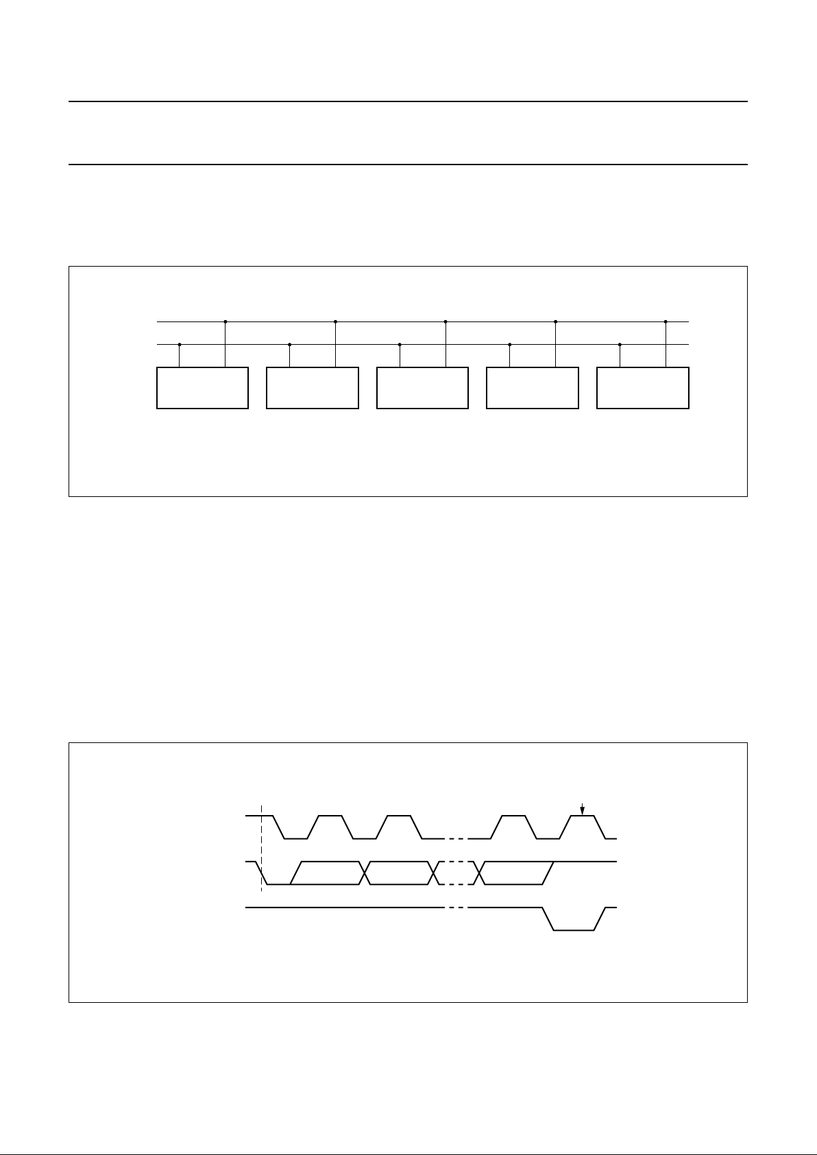
8.3 System configuration
A device generating a message is a ‘transmitter’, a device receiving a message is the ‘receiver’. The device that controls
the message is the ‘master’ and the devices which are controlled by the master are the ‘slaves’.
Fig.5 System configuration.
MBA605
MASTER
TRANSMITTER /
RECEIVER
SLAVE
RECEIVER
SLAVE
TRANSMITTER /
RECEIVER
MASTER
TRANSMITTER
MASTER
TRANSMITTER /
RECEIVER
SDA
SCL
8.4 Acknowledge
The number of data bytes transferred between the start
and stop conditions from transmitter to receiver is
unlimited. Each byte of eight bits is followed by an
acknowledge bit. The acknowledge bit is a HIGH level
signal put on the bus by the transmitter during which time
the master generates an extra acknowledge related clock
pulse. A slave receiver which is addressed must generate
an acknowledge after the reception of each byte. Also a
master receiver must generate an acknowledge after the
reception of each byte that has been clocked out of the
slave transmitter.
The device that acknowledges must pull down the SDA
line during the acknowledge clock pulse, so that the SDA
line is stable LOW during the HIGH period of the
acknowledge related clock pulse (set-up and hold times
must be taken into consideration). A master receiver must
signal an end of data to the transmitter by not generating
an acknowledge on the last byte that has been clocked out
of the slave. In this event the transmitter must leave the
data line HIGH to enable the master to generate a stop
condition.
Fig.6 Acknowledgement on the I2C-bus.
handbook, full pagewidth
MBA606 - 1
START
condition
S
SCL FROM
MASTER
DATA OUTPUT
BY TRANSMITTER
DATA OUTPUT
BY RECEIVER
clock pulse for
acknowledgement
1
2
8
9
 Loading...