

Philips N74ALS257N, N74ALS258DB, N74ALS258N, N74ALS258D, N74ALS257D Datasheet
74ALS257/74ALS258
Data selector/multiplexer
Product specification
IC05 Data Handbook
1991 Feb 08
INTEGRATED CIRCUITS
Philips Semiconductors Product specification
74ALS257/74ALS258Data selector/multiplexer
74ALS257 Quad 2-input data selector, non-inverting (3-State)
74ALS258 Quad 2-input data selector, inverting (3-State)
2
1991 Feb 08 853–1 130 01670
DESCRIPTION
The 74ALS257 is a quad 2-input multiplexer which selects 4 bits of
data from one of two sources under the control of a common select
input (S). The output enable input (OE
) is active when Low. When
OE
is High, all of the outputs (Yn) are forced to a High impedance
state (3-State) regardless of all other input conditions.
Moving data from two registers to a common output bus is a typical
use of the 74ALS257. The state of the select input determines the
particular register from which data comes.
The device is the logic implementation of 4-pole, 2-position switch
where the position of the switch is determined by the logic levels
supplied to the select input. The 74ALS258 is similar but has
inverting outputs (Y
n).
TYPE
TYPICAL
PROPAGATION DELAY
TYPICAL
SUPPLY CURRENT
(TOTAL)
74ALS257 7.0ns 7mA
74ALS258 7.0ns 7mA
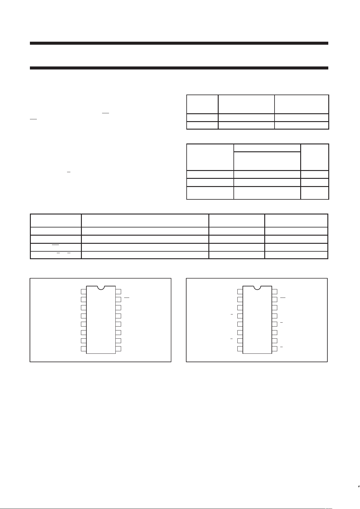
ORDERING INFORMATION
ORDER CODE
DESCRIPTION COMMERCIAL RANGE
V
CC
= 5V ±10%,
T
amb
= 0°C to +70°C
DRAWING
NUMBER
16-pin plastic DIP 74ALS257N, 74ALS258 SOT38-4
16-pin plastic SO 74ALS257D, 74ALS258D SOT109-1
16-pin plastic SSOP
Type II
74ALS257DB, 74ALS258DB SOT338-1
INPUT AND OUTPUT LOADING AND FAN-OUT TABLE
PINS DESCRIPTION
74ALS (U.L.)
HIGH/LOW
LOAD VALUE
HIGH/LOW
Ina, Inb, Inc, Ind Data inputs 1.0/1.0 20µA/0.1mA
S Select input 1.0/1.0 20µA/0.1mA
OE Enable input 1.0/1.0 20µA/0.1mA
Ya – Yd, Ya – Yd Data outputs 20/240 0.4mA/24mA
NOTE: One (1.0) ALS unit load is defined as: 20µA in the High state and 0.1mA in the Low state.
PIN CONFIGURATION – 74ALS257
16
15
14
13
12
11
107
6
5
4
3
2
1
Yb
V
CC
Yd
I0c
I1c
I1d
OE
I0d
S
I0a
I1b
I1a
Ya
I0b
98GND Yc
SF00673
PIN CONFIGURATION – 74ALS258
16
15
14
13
12
11
107
6
5
4
3
2
1
Y
b
V
CC
Yd
I0c
I1c
I1d
OE
I0d
S
I0a
I1b
I1a
Y
a
I0b
98GND Yc
SC00079
Philips Semiconductors Product specification
74ALS257/74ALS258Data selector/multiplexer
1991 Feb 08
3
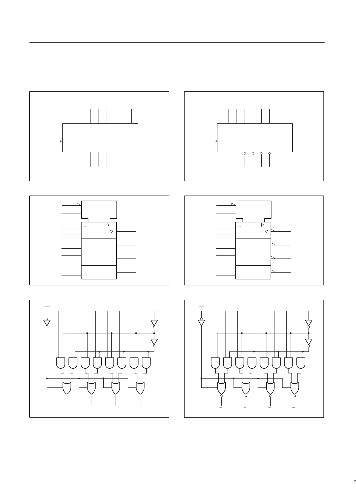
LOGIC SYMBOL – 74ALS257
VCC = Pin 16
GND = Pin 8
SF00674
1
15
S
OE
2356111014
I0a I1a I0b I1b I0c I1c I0d
Ya Yb Yc Yd
47912
13
I1d
LOGIC SYMBOL – 74ALS258
VCC = Pin 16
GND = Pin 8
SC00080
1
15
S
OE
2356111014
I0a I1a I0b I1b I0c I1c I0d
Ya Yb Yc Yd
47912
13
I1d
IEC/IEEE SYMBOL – 74ALS257
SF00675
2
1
15
EN
1
G1
3
4
1
MUX
5
6
7
10
11
9
13
14
12
IEC/IEEE SYMBOL – 74ALS258
SC00081
2
1
15
EN
1
G1
3
4
1
MUX
5
6
7
10
11
9
13
14
12
LOGIC DIAGRAM – 74ALS257
OE I0a I1a I0b I1b I0c I1c I0d I1d S
152356111014131
Ya Yb Yc Yd
47912
V
CC
= Pin 16
GND = Pin 8
SC00082
LOGIC DIAGRAM – 74ALS258
OE I0a I1a I0b I1b I0c I1c I0d I1d S
152356111014131
Y
aYbYcYd
47912
V
CC
= Pin 16
GND = Pin 8
SC00083
Philips Semiconductors Product specification
74ALS257/74ALS258Data selector/multiplexer
1991 Feb 08
4
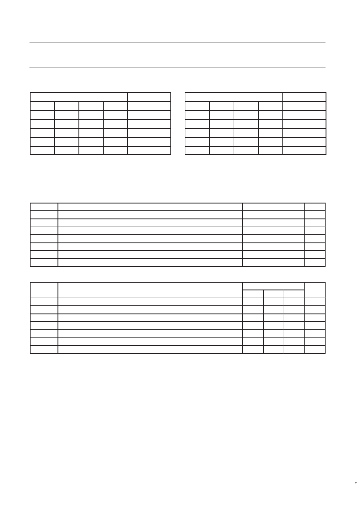
FUNCTION T ABLE – 74ALS257
INPUTS OUTPUT
OE S I0n I1n Yn
H X X X Z
L L L X L
L L H X H
L H X L L
L H X H H
H = High voltage level
L = Low voltage level
X = Don’t care
Z = High impedance “off” state
FUNCTION T ABLE – 74ALS258
INPUTS OUTPUT
OE S I0n I1n Yn
H X X X Z
L L L X H
L L H X L
L H X L H
L H X H L
H = High voltage level
L = Low voltage level
X = Don’t care
Z = High impedance “off” state
ABSOLUTE MAXIMUM RATINGS
(Operation beyond the limit set forth in this table may impair the useful life of the device.
Unless otherwise noted these limits are over the operating free air temperature range.)
SYMBOL
PARAMETER RATING UNIT
V
CC
Supply voltage –0.5 to +7.0 V
V
IN
Input voltage –0.5 to +7.0 V
I
IN
Input current –30 to +5 mA
V
OUT
Voltage applied to output in High output state –0.5 to V
CC
V
I
OUT
Current applied to output in Low output state 48 mA
T
amb
Operating free-air temperature range 0 to +70 °C
T
stg
Storage temperature range –65 to +150 °C
RECOMMENDED OPERATING CONDITIONS
LIMITS
SYMBOL
PARAMETER
MIN NOM MAX
UNIT
V
CC
Supply voltage 4.5 5.0 5.5 V
V
IH
High-level input voltage 2.0 V
V
IL
Low-level input voltage 0.8 V
I
IK
Input clamp current –18 mA
I
OH
High-level output current –2.6 mA
I
OL
Low-level output current 24 mA
T
amb
Operating free-air temperature range 0 +70 °C
 Loading...