

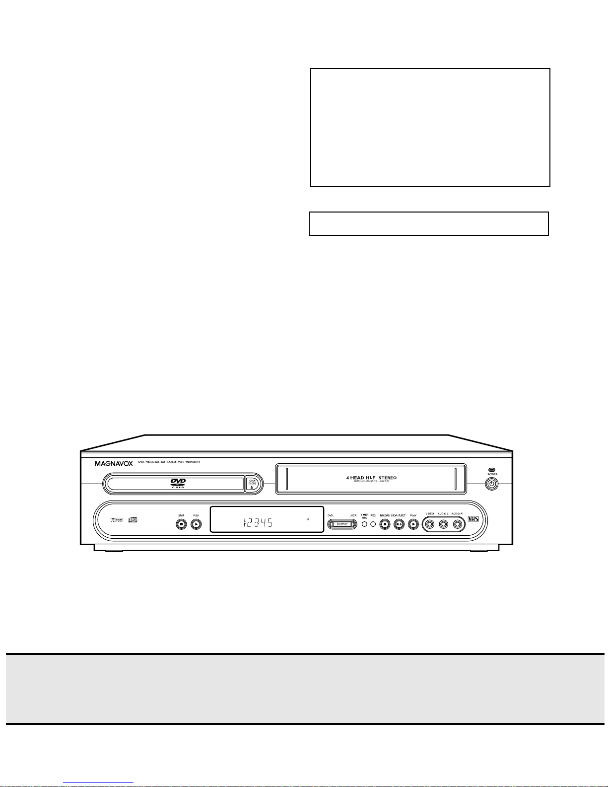
MANUAL 5881 Digital Video Disc Player & Video Cassette Recorder MAGNAVOX MDV530VR/17
Philips Consumer Electronics Company
A Division of Philips Electronics North America Corporation
Technical Service Data
Service So luti on s Grou p
Technical Publications Dept.
P.O. Box 555, 401 E. Old Andrew Johnson Hwy.
Jefferson City,TN 37760
Sec. 1A: Main Section
( MDV530VR/17 )
Specifications
Operating Instructions
Adjustment Procedures
Schematic Diagrams and CBA’s
Exploded Views
Cabinet & Electrical Parts Lists
Sec. 2: Deck Mechanism Secti o n
Digital Video Disc Player &
Video Cassette Recorder
MANUAL 5888
Service Manual
MAGNAVOX
Model: MDV530VR/17
Digital Video Disc Player & Video Cassette Recor der
First Issue: 3/03
2003 Philips Consumer Electronics Company
Philips Consumer Electronics Company
A Division of Philips Electronics North America Corporation
MANUAL 5888
Technical Service Data
Service So luti on s Grou p
Technical Publications Dept.
P.O. Box 555, 401 E. Old Andrew Johnson Hwy.
Jefferson City,TN 37760
Sec. 1A: Main Section
( MDV530VR/17 )
Specifications
Operating Instructions
Adjustment Procedures
Schematic Diagrams and CBA’s
Exploded Views
Cabinet & Electrical Parts Lists
Digital Video Disc Player &
Video Cassette Recorder
Service Manual
Digital Video Disc Player & Video Cassette Recor der
First Issue: 3/03
2003 Philips Consumer Electronics Company
MAGNAVOX
Model: MDV530VR/17

IMPORTANT SAFETY NOTICE
Proper service and repair is important to the safe, reliable operation of all
Philips Consumer Electronics Com pany** Equipment. The service pr ocedures
recommended by Philips and described in this service manual are effective
methods of performing service operations. Some of these service operations
require the use of tools specially designed for the purpose. The special tools
should be used when and as recommended.
It is important to note that this manual contains various CAUTIONS and
NOTICES which should be carefully read in order to minimize the risk of personal injury to service personnel. The possibility exists that improper service
methods may damage the equipment. It also is important to understand that
these CAUTIONS and NOTICES ARE NOT EXHAUSTIVE. Philips could not
possibly know, evaluate and advise the service trade of all conceivable ways
in which service might be done or of the possible hazardous consequences of
each way. Consequently, Philips has not undertaken any such broad evaluation. Accordingly, a servicer who uses a service procedure or tool which is
not recommended by Philips must first satisfy himself thoroughly that neither
his safety nor the safe operation of the equipment will be jeopardized by the
service method selected.
** Hereafter throughout this manual, Philips Consumer Electronics Company
will be referred to as Philips.
WARNING
Critical components having special safety characteristics are identified
with a # by the Ref. No. in the parts list and enclosed within a broken
line* (where several critical components are grouped in one area) along
with the safety symbol # on the schematics or exploded views.
Use of substitute replacement parts which do not have the same specifie d
safety characteristics may create shock, fire, or other hazards.
Under no circumstances should the original design be modified or altered
without written permission from Philips. Philips assumes no liability,
express or implied, arising out of any unauthorized modification of
design. Servicer assumes all liability.
* Broken Line
Manufactured under license from Dolby Laboratories. "Dolby"
and the double-D symbol are trademarks of Dolby Laboratories.

TABLE OF CONTENTS
[ Main Section ]
Page
SPECIFICATIONS . . . . . . . . . . . . . . . . . . . . . . . . . . . . . . . . . . . . . . . . . . . . . . . . . . . . . . . . . . . . . . . . . . . . . . . 1-1-1
LASER BEAM SAFETY PRECAUTIONS. . . . . . . . . . . . . . . . . . . . . . . . . . . . . . . . . . . . . . . . . . . . . . . . . . . . . . 1-2-1
IMPORTANT SAFETY PRECAUTIONS. . . . . . . . . . . . . . . . . . . . . . . . . . . . . . . . . . . . . . . . . . . . . . . . . . . . . . . 1-3-1
STANDARD NOTES FOR SERVICING . . . . . . . . . . . . . . . . . . . . . . . . . . . . . . . . . . . . . . . . . . . . . . . . . . . . . . . 1-4-1
PREPARATION FOR SERVICING . . . . . . . . . . . . . . . . . . . . . . . . . . . . . . . . . . . . . . . . . . . . . . . . . . . . . . . . . . . 1-5-1
OPERATING CONTROLS AND FUNCTIONS. . . . . . . . . . . . . . . . . . . . . . . . . . . . . . . . . . . . . . . . . . . . . . . . . . 1-6-1
REMOTE CONTROL OPERATION . . . . . . . . . . . . . . . . . . . . . . . . . . . . . . . . . . . . . . . . . . . . . . . . . . . . . . . . . . 1-7-1
CABINET DISASSEMBLY INSTRUCTIONS . . . . . . . . . . . . . . . . . . . . . . . . . . . . . . . . . . . . . . . . . . . . . . . . . . . 1-8-1
ELECTRICAL ADJUSTMENT INSTRUCTIONS . . . . . . . . . . . . . . . . . . . . . . . . . . . . . . . . . . . . . . . . . . . . . . . . 1-9-1
Adjustment Points and Test Points . . . . . . . . . . . . . . . . . . . . . . . . . . . . . . . . . . . . . . . . . . . . . . . . . . . . . . . . 1-9-2
FIRMWARE RENEWAL MODE . . . . . . . . . . . . . . . . . . . . . . . . . . . . . . . . . . . . . . . . . . . . . . . . . . . . . . . . . . . . . 1-10-1
BLOCK DIAGRAM
Servo/System Control Block Diagarm. . . . . . . . . . . . . . . . . . . . . . . . . . . . . . . . . . . . . . . . . . . . . . . . . . . . . . 1-11-1
Video Block Diagarm. . . . . . . . . . . . . . . . . . . . . . . . . . . . . . . . . . . . . . . . . . . . . . . . . . . . . . . . . . . . . . . . . . . 1-11-3
Audio Block Diagram. . . . . . . . . . . . . . . . . . . . . . . . . . . . . . . . . . . . . . . . . . . . . . . . . . . . . . . . . . . . . . . . . . . 1-11-5
Hi-Fi Block Diagram. . . . . . . . . . . . . . . . . . . . . . . . . . . . . . . . . . . . . . . . . . . . . . . . . . . . . . . . . . . . . . . . . . . . 1-11-7
Power Supply Block Diagram . . . . . . . . . . . . . . . . . . . . . . . . . . . . . . . . . . . . . . . . . . . . . . . . . . . . . . . . . . . . 1-11-9
DVD System Control/Servo Block Diagram. . . . . . . . . . . . . . . . . . . . . . . . . . . . . . . . . . . . . . . . . . . . . . . . . . 1-11-11
Digital Signal Process Block Diagram. . . . . . . . . . . . . . . . . . . . . . . . . . . . . . . . . . . . . . . . . . . . . . . . . . . . . . 1-11-13
DVD Video/Audio Block Diagram . . . . . . . . . . . . . . . . . . . . . . . . . . . . . . . . . . . . . . . . . . . . . . . . . . . . . . . . . 1-11-15
SCHEMATIC DIAGRAM/CBA’S AND TEST POINTS
Main 1/8 Schematic Diagram Parts Location Guide . . . . . . . . . . . . . . . . . . . . . . . . . . . . . . . . . . . . . . . . . . . 1-12-2
Main 1/8 Schematic Diagram . . . . . . . . . . . . . . . . . . . . . . . . . . . . . . . . . . . . . . . . . . . . . . . . . . . . . . . . . . . . 1-12-3
Main 2/8 Schematic Diagram . . . . . . . . . . . . . . . . . . . . . . . . . . . . . . . . . . . . . . . . . . . . . . . . . . . . . . . . . . . . 1-12-5
Main 2/8 Schematic Diagram Parts Location Guide . . . . . . . . . . . . . . . . . . . . . . . . . . . . . . . . . . . . . . . . . . . 1-12-7
Main 3/8 Schematic Diagram Parts Location Guide . . . . . . . . . . . . . . . . . . . . . . . . . . . . . . . . . . . . . . . . . . . 1-12-8
Main 3/8 Schematic Diagram . . . . . . . . . . . . . . . . . . . . . . . . . . . . . . . . . . . . . . . . . . . . . . . . . . . . . . . . . . . . 1-12-9
Main 4/8 Schematic Diagram . . . . . . . . . . . . . . . . . . . . . . . . . . . . . . . . . . . . . . . . . . . . . . . . . . . . . . . . . . . . 1-12-11
Main 4/8 Schematic Diagram Parts Location Guide . . . . . . . . . . . . . . . . . . . . . . . . . . . . . . . . . . . . . . . . . . . 1-12-13
Main 5/8 Schematic Diagram Parts Location Guide . . . . . . . . . . . . . . . . . . . . . . . . . . . . . . . . . . . . . . . . . . . 1-12-14
Main 5/8 Schematic Diagram . . . . . . . . . . . . . . . . . . . . . . . . . . . . . . . . . . . . . . . . . . . . . . . . . . . . . . . . . . . . 1-12-15
Main 6/8 Schematic Diagram/Parts Location Guide . . . . . . . . . . . . . . . . . . . . . . . . . . . . . . . . . . . . . . . . . . . 1-12-17
Main 7/8 Schematic Diagram/Parts Location Guide . . . . . . . . . . . . . . . . . . . . . . . . . . . . . . . . . . . . . . . . . . . 1-12-19
Main 8/8 Schematic Diagram . . . . . . . . . . . . . . . . . . . . . . . . . . . . . . . . . . . . . . . . . . . . . . . . . . . . . . . . . . . . 1-12-21
Main 8/8 Schematic Diagram Parts Location Guide . . . . . . . . . . . . . . . . . . . . . . . . . . . . . . . . . . . . . . . . . . . 1-12-23
Function Schematic Diagram/Parts Location Guide . . . . . . . . . . . . . . . . . . . . . . . . . . . . . . . . . . . . . . . . . . . 1-12-24
Main CBA Top View <BH9400F01013A> . . . . . . . . . . . . . . . . . . . . . . . . . . . . . . . . . . . . . . . . . . . . . . . . . . . 1-12-25
Main CBA Bottom View <BH9400F01013A> . . . . . . . . . . . . . . . . . . . . . . . . . . . . . . . . . . . . . . . . . . . . . . . . 1-12-27
Main CBA Parts Location Guide . . . . . . . . . . . . . . . . . . . . . . . . . . . . . . . . . . . . . . . . . . . . . . . . . . . . . . . . . . 1-12-29
Function CBA & DVD OP/CL CBA Top/Bottom View . . . . . . . . . . . . . . . . . . . . . . . . . . . . . . . . . . . . . . . . . . 1-12-31
Power Supply Schematic Diagram . . . . . . . . . . . . . . . . . . . . . . . . . . . . . . . . . . . . . . . . . . . . . . . . . . . . . . . . 1-12-33
Power Supply Schematic Diagram/CBA Parts Location Guide. . . . . . . . . . . . . . . . . . . . . . . . . . . . . . . . . . . 1-12-35
Power Supply CBA Top/Bottom View <BH9400F01021A,B> . . . . . . . . . . . . . . . . . . . . . . . . . . . . . . . . . . . . 1-12-37
Power Supply CBA Top/Bottom View <BH9400F01022A,B> . . . . . . . . . . . . . . . . . . . . . . . . . . . . . . . . . . . . 1-12-39
DVD Main 1/3 Schematic Diagram . . . . . . . . . . . . . . . . . . . . . . . . . . . . . . . . . . . . . . . . . . . . . . . . . . . . . . . . 1-12-41
IC101 Voltage Chart . . . . . . . . . . . . . . . . . . . . . . . . . . . . . . . . . . . . . . . . . . . . . . . . . . . . . . . . . . . . . . . . . . . 1-12-43
DVD Main 2/3 Schematic Diagram . . . . . . . . . . . . . . . . . . . . . . . . . . . . . . . . . . . . . . . . . . . . . . . . . . . . . . . . 1-12-45
DVD Main 3/3 Schematic Diagram . . . . . . . . . . . . . . . . . . . . . . . . . . . . . . . . . . . . . . . . . . . . . . . . . . . . . . . . 1-12-47
WAVEFORMS . . . . . . . . . . . . . . . . . . . . . . . . . . . . . . . . . . . . . . . . . . . . . . . . . . . . . . . . . . . . . . . . . . . . . . . . . . 1-13-1
WIRING DIAGRAM (VCR SECTION) . . . . . . . . . . . . . . . . . . . . . . . . . . . . . . . . . . . . . . . . . . . . . . . . . . . . . . . . 1-14-1
WIRING DIAGRAM (DVD SECTION). . . . . . . . . . . . . . . . . . . . . . . . . . . . . . . . . . . . . . . . . . . . . . . . . . . . . . . . . 1-14-3
SYSTEM CONTROL TIMING CHARTS. . . . . . . . . . . . . . . . . . . . . . . . . . . . . . . . . . . . . . . . . . . . . . . . . . . . . . . 1-15-1
IC PIN FUNCTION . . . . . . . . . . . . . . . . . . . . . . . . . . . . . . . . . . . . . . . . . . . . . . . . . . . . . . . . . . . . . . . . . . . . . . . 1-16-1
LEAD IDENTIFICATIONS. . . . . . . . . . . . . . . . . . . . . . . . . . . . . . . . . . . . . . . . . . . . . . . . . . . . . . . . . . . . . . . . . . 1-17-1
ELECTRICAL PARTS LIST . . . . . . . . . . . . . . . . . . . . . . . . . . . . . . . . . . . . . . . . . . . . . . . . . . . . . . . . . . . . . . . . 1-18-1
EXPLODED VIEWS . . . . . . . . . . . . . . . . . . . . . . . . . . . . . . . . . . . . . . . . . . . . . . . . . . . . . . . . . . . . . . . . . . . . . . 1-19-1
MECHANICAL PARTS LIST. . . . . . . . . . . . . . . . . . . . . . . . . . . . . . . . . . . . . . . . . . . . . . . . . . . . . . . . . . . . . . . . 1-20-1

SPECIFICATIONS
< VCR Section >
Description Unit Minimum Nominal Maximum Remark
1. Video
1-1. Video Output (PB) Vp-p 0.8 1.0 1.2 SP Mode
1-2. Video Output (R/P) Vp-p 0.8 1.0 1.2
1-3. Video S/N Y (R/P) dB 40 48 SP Mode
1-4. Video Color S/N AM (R/P) dB 38 44 SP Mode
1-5. Video Color S/N PM (R/P) dB 36 40 SP Mode
1-6. Resolution (R/P) Line 220 240 SP Mode
2. Servo
2-1. Jitter Low (R/P) µsec 0.05 0.15 SP Mode
2-2. Wow & Flutter (R/P) % 0.15 0.35 SP Mode
3. Normal Audio
3-1. Output (PB) dBV -10 -6 -2 SP Mode
3-2. Output (R/P) dBV -10 -6 -2 SP Mode
3-3. S/N (R/P) dB 40 44 SP Mode
3-4. Distortion (R/P) % 1.5 5.0 SP Mode
3-5. Freq. Response (R/P) at 100Hz dB -9.5 -3.5 2.5 SP Mode
(-20dB ref. 1kHz) at 8kHz dB -6.5 -0.5 5.5 SP Mode
4. Tuner
4-1. Video output (E-E) Vp-p 0.8 1.0 1.2 E-E Mode
4-2. Video S/N (E-E) dB 40 46 E-E Mode
4-3. Audio output (E-E) dBV -10 -6 -2 E-E Mode
4-4. Audio S/N (E-E) dB 40 44 E-E Mode
5. Hi-Fi Audio
5-1. Output (PB) dBV -12 -8 -4 SP Mode
5-2. Output (R/P) dBV -12 -8 -4 SP Mode
5-3. S/N (A WTD) dB 70 SP Mode
5-4. Freq. Response at 20Hz dB -4 0 +4 SP Mode
at 20kHz dB -4 0 +4 SP Mode
Other Specifications
Operating Temperature
Relative Humidity
Power Requirements
Power Consumption
Dimensions
Weight
: 41°F ( 5°C ) to 104°F ( 40°C )
: 30% to 80%
: AC 120 V, 60 Hz
: 24 W
: 17-1/8” (W) x 3-7/8” (H) x 10-1/2” (D)
/ 435 mm (W) x 99 mm (H) x 266 mm (D)
: 8.8 lbs. (4.0 kg)
Test Tape ..... VFMS0001H6
Note: Nominal specs represent the desi gn spec s. All units should be able to approximate the se. Some will exceed
and some may drop slightly below these specs. Limit s pecs represent the ab solute worst conditi on that still might
be considered acceptable. In no case should a unit fail to meet limit specs.
1-1-1 H9460SP

< DVD Section >
ITEM CONDITIONS UNIT NOMINAL LIMIT
1. Video Output 75 ohm load Vpp 1.0 ± 0.1
2. Coaxial Digital Out 75 ohm load mVpp 500 ± 100
3. Audio (PCM)
3-1. Output Level 1kHz 0dB Vrms 2.0
3-2. S/N dB 120
3-3. Freq. Response
DVD fs=48kHz 20~22kHz dB ± 0.5
CD fs=44.1kHz 20~20 kHz dB ± 0.5
3-4. THD+N
DVD 1 kHz 0dB % 0.0025
CD 1 kHz 0dB % 0.003
NOTES:
1. All Items are measured without pre-emphasis unless otherwise specified.
2. Power supply : AC120 V 60 Hz
3. Load imp. : 100 K ohm
4. Room ambient : +25
°C
1-1-2 H9460SP

D
LASER BEAM SAFETY PRECAUTIONS
This DVD player uses a pickup that emits a laser beam.
Do not look directly at the l aser beam coming
from the pickup or allo w it t o str ike agai nst your
skin.
The laser beam is emitted from the locatio n shown in the figure. When ch ecking the laser d iode, be sure to keep
your eyes at least 30cm away from the pickup lens when the diode is tur ned on. Do not loo k directly at the laser
beam.
Caution: Use of controls an d adjustments, or doing pr ocedures other than th ose specified here in, may result in
hazardous radiation exposure.
rive Mecha Assembly
Laser Beam Radiation
Laser Pickup
Turntable
CAUTION
LASER RADIATION
WHEN OPEN. DO NOT
STARE INTO BEAM.
Location: Inside Top of DVD mechanism.
1-2-1 DVD_LASER

IMPORTANT SAFETY PRECAUTIONS
Product Safety Notice
Some electrical and mechanical parts have special
safety-related characteristics which are often not evident from visual inspection, nor can the protection they
give necessarily be obtained by replacing them with
components rated for higher voltage, wattage, etc.
Parts that have special safety characteristics are identified by a # on schematics and in parts lists. Use of a
substitute replacement that does not have the same
safety characteristics as the recommended replacement par t might create shock, fire, and/or other h azards. The Product’s Safety is under review
continuously and new instructions are issued whenever appropriate. Prior to shipment from the factory,
our products are carefully inspected to confirm with
the recognized product safety and electrical codes of
the countries in which they are to be sold. However, in
order to maintain such compli ance, it is equall y impor tant to implement the following precautions when a set
is being serviced.
Precautions during Servicing
A. Parts identified by the # symbol are critical for
safety. Replace only with part number specified.
B. In addition to safety, other parts and assemblies
are specified for conformance with regulations
applying to spurious radiation. These must also be
replaced only with specified re pla ce men ts.
Examples: RF converters, RF cables, noise blocking capacitors, and noise blocking filters, etc.
C. Use specified internal wiring. Note especially:
1)Wires covered with PVC tubing
2)Double insulated wires
3)High voltage leads
D. Use specified insulating materials for hazardous
live parts. Note especially:
1)Insulation tape
2)PVC tubing
3)Spacers
4)Insulators for transistors
E. When replacing AC primary side components
(transformers, power cord, etc.), wrap ends of
wires securely about the terminals before soldering.
F. Observe that the wires do not conta ct heat produc -
ing parts (heats inks, oxide metal fil m resis tors, fusible resistors, etc.).
G. Check that replaced wires do not contact sharp
edges or pointed parts.
H. When a power cord has been replaced, check that
5 - 6 kg of force in any direction will not loosen it.
I. Also check areas surrounding repair ed locations.
J. Be careful that foreign objects (screws, solder
droplets, etc.) do not remain inside the set.
K. Crimp type wire connector
The power transformer uses cri mp type con nector s
which connect the power cord and the primary side
of the transformer. When replacing the transformer,
follow these steps carefully and precisely to prevent
shock hazards.
Replacement procedure
1)Remove the old connector by cutting the wires at a
point close to the connector.
Important: Do not re-use a connector. (Discard it.)
2)Strip about 15 mm of the insulation from the ends
of the wires. If the wires are stranded, twist the
strands to avoid frayed conductors.
3)Align the lengths of the wires to be connected.
Insert the wires fully into the connector.
4)Use a crimping tool to crimp the metal sleeve at its
center. Be sure to crimp fully to t he complete closure of the tool.
L. When connecting or disconnecting the internal
connectors, first, disc onnect the AC plug from the
AC outlet.
1-3-1 DVD_SFN1
r
e)
Safety Check afte r Servicing
Examine the area surrounding the repaired location for
damage or deteri oration. Observe that screws, par ts,
and wires have been returned to their original positions. Afterwards, do the following tests and confirm
the specified values to verify compliance with safety
standards.
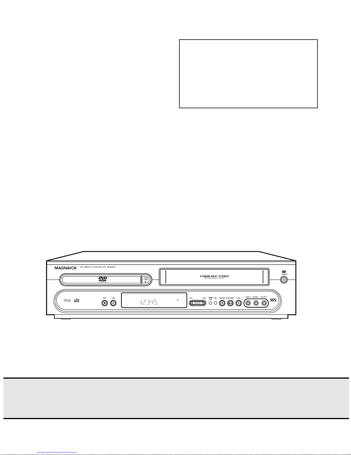
1. Clearance Distance
When replacing primary circuit components, confirm
specified clearanc e distance (d ) and (d’) be tween soldered terminals, and between terminals and surrounding metallic parts. (See Fig. 1)
Table 1 : Ratings for selected area
AC Line Voltage Clearance Distance (d) (d’)
Chassis or Secondary Conducto
Primary Circuit Terminals
dd'
120 V
Note: This table is unofficial and for reference only.
Be sure to confirm the precise values.
2. Leakage Current Test
Confirm the specified (or lower) leakage current
between B (earth ground, power cord plug prongs)
and externally exposed accessible parts (RF terminals, antenna terminals, video and audio input and
output terminals, microphone jacks, earphone jacks,
etc.) is lower than or equal to the specified value in the
table below.
Measuring Method (Power ON) :
Insert load Z between B (earth ground, power cord
plug prongs) and exposed accessible parts. Use an
AC voltmeter to measure across the ter minals of load
Z. See Fig. 2 and the following table.
Table 2: Leakage current ratings for selected areas
AC Line Voltage Load Z Leakage Current (i) Earth Ground (B) to:
120 V
≥ 3.2mm (0.126 inches)
0.15µF CAP. & 1.5kΩ RES.
Connected in parallel
Exposed Accessible Part
Z
1.5k
i≤0.5mA Peak Exposed accessible parts
0.15 F
Earth Ground
B
Power Cord Plug Prongs
AC Voltmeter
(High Impedanc
Fig. 1
Fig. 2
Note: This table is unofficial and for reference only. Be sure to confirm the precise values.
1-3-2 DVD_SFN1
STANDARD NOTES FOR SERVICING
O
P
P
Circuit Board Indications
a. The output pin of the 3 pin Regulator ICs is indi-
cated as shown.
Top View
Input
ut
b. For other ICs, pin 1 and every fifth pin are indicated
as shown.
In
in 1
c. The 1st pin of every ma le c on nec tor i s indi ca ted a s
shown.
in 1
Bottom View
5
10
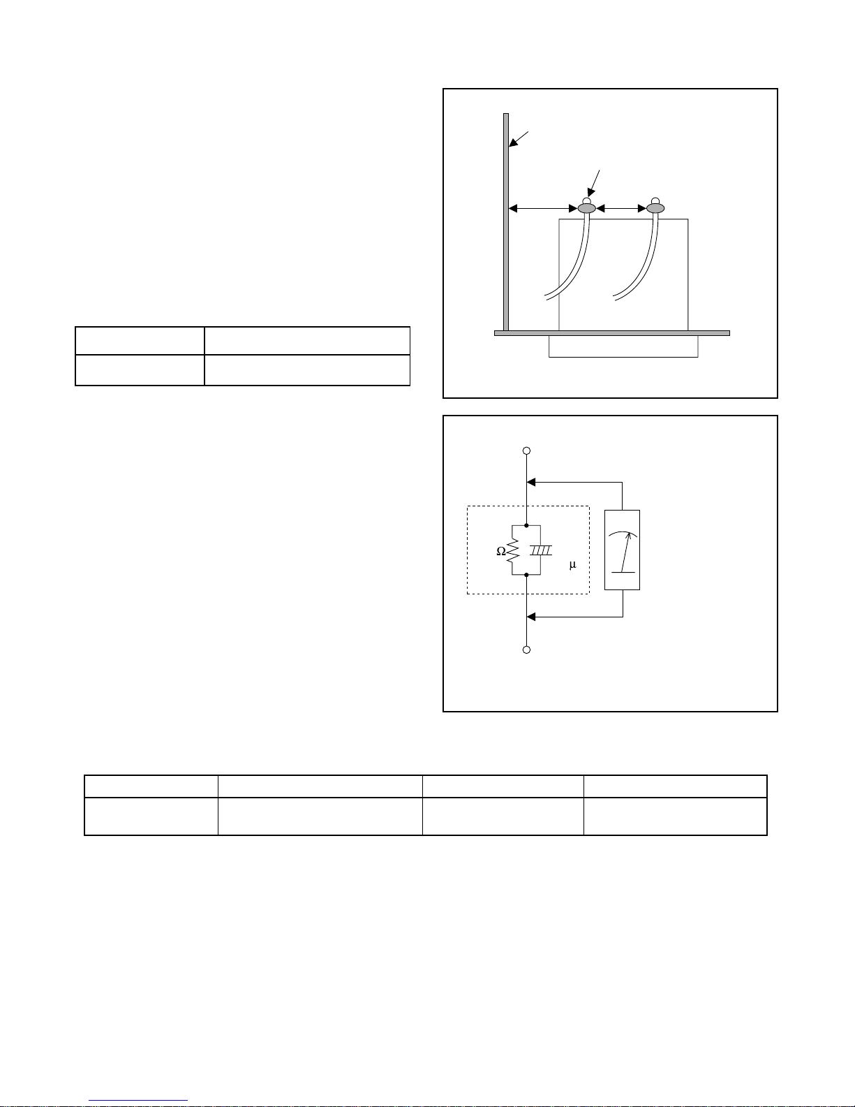
How to Remove / Install Flat Pack-IC
1. Removal
With Hot-Air Flat Pack-IC Desoldering Machine:.
(1) Prepare the hot-air flat pack-IC desoldering
machine, then apply hot air to the Flat Pack-IC
(about 5 to 6 seconds). (Fig. S-1-1)
Fig. S-1-1
(2) Remove the flat pack-IC with tweezers while apply-
ing the hot air.
(3) Bottom of the flat pack-IC i s fixed with glue to the
CBA; when rem oving enti re flat pa ck-IC, first apply
soldering iron to ce nter of the flat pack-IC and hea t
up. Then remove (glue will be melted). (Fig. S-1-6)
(1) Release the flat pack-IC from th e CBA usin g twee-
zers. (Fig. S-1-6)
Caution:
Instructions for Connectors
1. When you conn ect or disconn ect t he FFC (Flexible
Foil Connector) cable, be sure to first disconnect
the AC cord.
2. FFC (Flexible Foil Connector) cable should be
inserted parallel into the connector, not at an angle.
FFC Cable
Connector
CBA
* Be careful to avoid a short circuit.
1. D o not supply hot air to the chip par ts around the
flat pack-IC for over 6 seconds because damage to
the chip parts may occur. Put masking tape around
the flat pack-IC to protect other parts from damage.
(Fig. S-1-2)
2. The flat pack-IC on the CBA is affixed with glue, so
be careful not to brea k or damage the foil of each
pin or the solder lands under the IC when removing
it.
Hot-air
Flat Pack-IC
Desoldering
CBA
Masking
Tape
Tweezers
Machine
Flat Pack-IC
Fig. S-1-2
1-4-1 DVD_NOTE
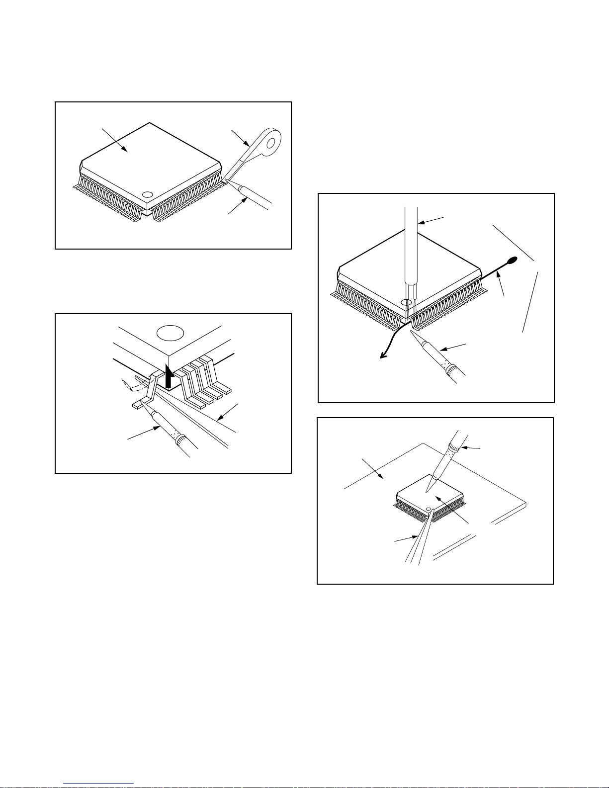
With Soldering Iron:
F
F
S
rp
or
n
(1)Using desoldering braid, remove the sol der from al l
pins of the flat pack-IC. When you use solder flux
which is applied to all pins of the flat pack-IC, you
can remove it easily. (Fig. S-1-3)
lat Pack-IC
Desoldering Braid
(4) Bottom of the flat pack-IC i s fixed with glue to the
CBA; when rem oving enti re flat pa ck-IC, first apply
soldering iron to ce nter of the flat pack-IC and hea t
up. Then remove (glue will be melted). (Fig. S-1-6)
(5) Release the flat pack-IC from th e CBA usin g twee-
zers. (Fig. S-1-6)
Note:
When using a solder ing iron, care must be taken
to ensure that the flat pack-IC is not bei ng held by
glue. When the flat pack-IC is removed from the
CBA, handle it gently beca use it may be damaged
if force is applied.
Soldering Iron
Hot Air Blower
Fig. S-1-3
(2) Lift each lead of the flat pack-IC upward one by
one, using a shar p pin or wire to which s older will
not adhere (iron wi re). When he ating the pins, us e
a fine tip soldering iron or a hot air desoldering
machine. (Fig. S-1-4)
Iron Wire
Soldering Iron
To Solid
Mounting Point
Fig. S-1-5
Sha
Pin
ine Tip
oldering Iron
Fig. S-1-4
CBA
Fine Tip
Soldering Iro
(3)B ottom of the flat pack-IC is fixed with glue to the
CBA; when removing entire flat pack-IC, first apply
soldering iron to c en ter of the flat pack-IC and heat
up. Then remove (glue will be melted). (Fig. S-1-6)
(4)Re lease the fl at pack-IC from the CBA using twee-
zers. (Fig. S-1-6)
Tweezers
Flat Pack-IC
With Iron Wire:
(1)Using desoldering braid, remove the sol der from al l
Fig. S-1-6
pins of the flat pack-IC. When you use solder flux
which is applied to all pins of the flat pack-IC, you
can remove it easily. (Fig. S-1-3)
(2) Affix the wire to a workbench or solid mounting
point, as shown in Fig. S-1-5.
(3) While heating the pins using a fine tip soldering
iron or hot air blower, pull up the wire as the solde r
melts so as to lift the IC leads from the CBA contact
pads as shown in Fig. S-1-5
1-4-2 DVD_NOTE
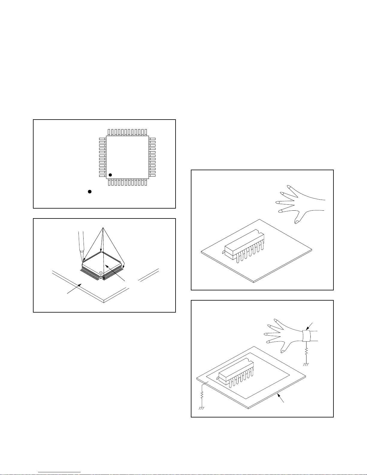
2. Installation
P
i
d
(1) Using desoldering braid, remove the solder from
the foil of each pin of the flat pack-IC on the CBA
so you can install a replacement fla t pack-IC more
easily.
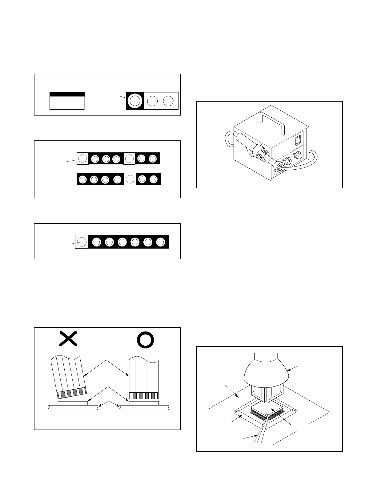
(2) The “I” mark on the flat pack-IC indicates pin 1.
(See Fig. S-1-7.) Be s ure this mark matches the 1
on the PCB when positioni ng for installation. Then
presolder the four cor ners of the fl at pack-IC. (See
Fig. S-1-8.)
(3)Solder all pins of the flat pack-IC. Be sure that none
of the pins have solder bridges.
Example :
in 1 of the Flat Pack-IC
s indicated by a " " mark.
Fig. S-1-7
Instructions for Handling
Semi-conductors
Electrostatic breakdown of the semi-conductors may
occur due to a potential di fference caused by electrostatic charge during unpacking or repair work.
1. Ground for Human Body
Be sure to wear a groun ding band (1M Ω) that is properly grounded to re move any static electr ici ty that may
be charged on the body.
2. Ground for Workbench
(4) Be sure to place a conductive sheet or copper plate
with proper grounding (1MΩ) on the workbench or
other surface, where the semi-conductors are to be
placed. Because the static electricity charge on
clothing will not escape thr ough the body grounding band, be careful t o avoid contacting semi-conductors with your clothing.
< Incorrect >
CBA
Presolder
Flat Pack-IC
Fig. S-1-8
CBA
< Correct >
Grounding Ban
1MΩ
CBA
1MΩ
Conductive Sheet or
Copper Plate
1-4-3 DVD_NOTE
PREPARATION FOR SERVICING
How to Enter the Service Mode
About Optical Sensors
Caution:
An optical sensor system is used for the Tape Start
and End Sensors on this equipment. Carefully read
and follow the instructions below. Otherwise the unit
may operate erratically.
What to do for preparation
Insert a tap e into the Deck Mechan ism Assembly and
press the PLAY button. The tape will be loaded into
the Deck Mechanism Assembly. Make sure the power
is on, TP502 (SENSOR INHIBITION) to GND. This will
stop the function of Tape Start Sensor, Tap e E nd Sen sor and Reel Sensors. (If these TPs are connected
before plugging in the unit, the function of the sens ors
will stay valid.) See Fig. 1.
Q503
Q504
TP502
S-INH
Fig. 1
Note: Because the Tape End Sensors are inactive, do
not run a tape all the way to the start or the en d of the
tape to avoid tape damage.
1-5-1 H9400PFS
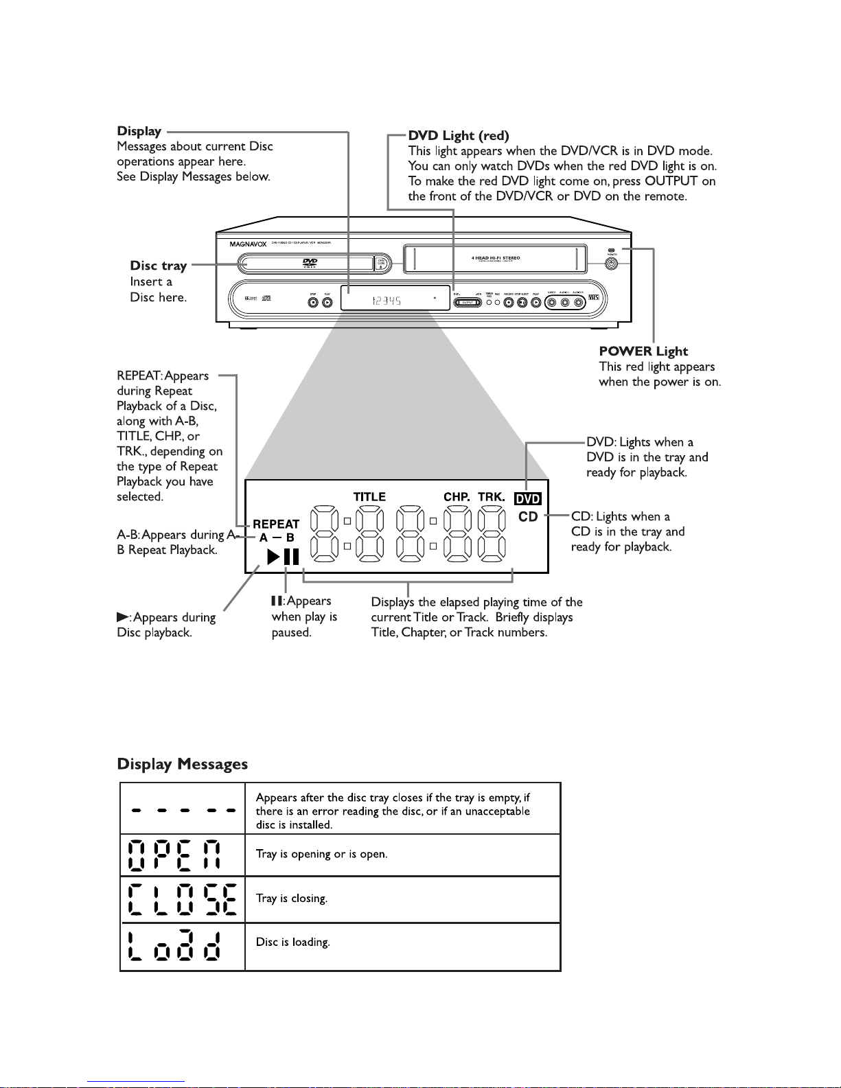
OPERATING CONTROLS AND FUNCTIONS
1-6-1 H9460IB

1-6-2 H9460IB
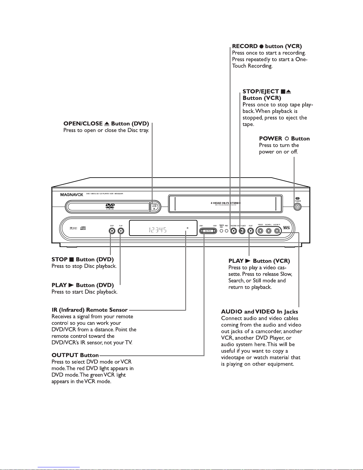
1-6-3 H9460IB
1-6-4 H9460IB
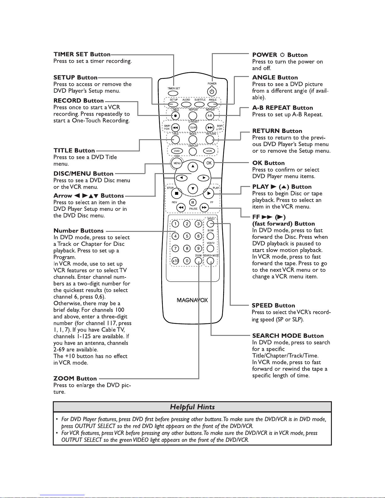
REMOTE CONTROL OPERATION
1-7-1 H9460IBR

1-7-2 H9460IBR
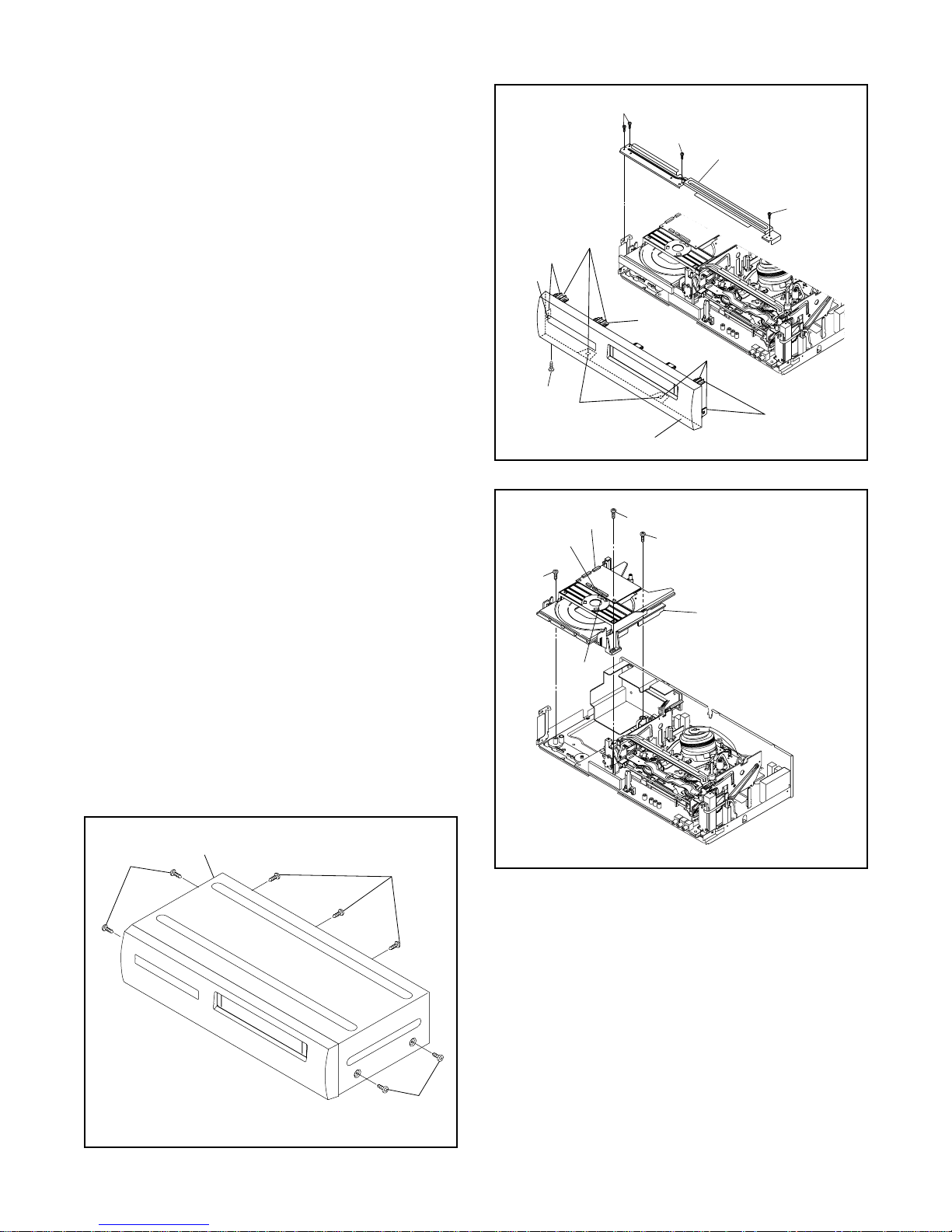
CABINET DISASSEMBLY INSTRUCTIONS
1. Disassembly Flowchart
This flowchart indicates the disassembly steps to gain
access to item(s) to be ser vic ed. When reasse mbling,
follow the steps in reverse order. Bend, route, and
dress the cables as they were originally.
[1] Top Cover
[2] Front
Assembly
[16] Side
Bracket
[5] DVD Main
CBA Unit
[13] DVD OP/CL
CBA
[12] Main CBA
[14] Function
CBA
[3] Top Bracket
[4] DVD Mecha
Assembly
[6] Rear Unit
[10] VCR
Chassis Unit
[15] Deck
Pedestal
[9] Rear Panel
[8] PCB Bracket
[7] Power
Supply CBA
[11] Deck
Assembly
2. Disassembly Method
REMOVAL
ID/
LOC.
PART
No.
[1] Top Cover D1 7(S-1) -
Front
[2]
Assembly
Top
[3]
Bracket
DVD
[4]
Mecha
Assembly
DVD Main
[5]
CBA Unit
REMOVE/*UNHOOK/
Fig.
UNLOCK/RELEASE/
No.
UNPLUG/DESOLDER
D2 (S-3), *7(L-1)
D2 4(S-2) -
3(S-4), *CN401,
D3
*CN302, *CN601
2(S-5), *CN201,
D4
*CN301
Note
1
1-1
1-2
-
2
2-1
2-2
2-3
3
REMOVAL
ID/
LOC.
No.
[7]
[8]
[9]
PART
Power
Suppy CBA
PCB
Brackt
Rear Panel
REMOVE/*UNHOOK/
Fig.
UNLOCK/RELEASE/
No.
UNPLUG/DESOLDER
D6 4(S-8) -
D6 3(S-9) -
D6 ---------- -
Note
VCR
[10]
Chassis
D7 5(S-10), 4(S-11) -
Unit
Deck
[11]
Assembly
D8 Desolder, 2(S-12) 4,5
[12] Main CBA D8 ---------- -
DVD OP/
[13]
[14]
[15]
[16]
↓
(1)
CL CBA
Function
CBA
Deck
Pedestal
Side
Bracket
↓
(2)
D8 ---------- -
D8 ---------- -
D9 7(S-13) -
D9 (S-14) -
↓
(3)
↓
(4)
↓
(5)
Note:
(1): Identification (location) No. of parts in the figures
(2):Name of the part
(3):Figure Number for reference
(4): Identification of parts to be removed, unhooked,
unlocked, released, unplugged, unclamped, or
desoldered.
P=Spring, L=Locking Tab, S=Screw,
CN=Connector
*=Unhook, Unlock, Release, Unplug, or Desolder
e.g. 2(S-2) = two Screws (S-2),
2(L-2) = two Locking Tabs (L-2)
(5): Refer to “Reference Notes.”
[6] Rear Unit D5
5(S-6), 3(S-7),
CN1005
-
1-8-1 H9460DC
Reference Notes
(
(
ly
CAUTION 1: Locking Tabs (L -1) are fra gile. Be caref ul
not to break them.
1-1. Remove Screw (S-3).
1-2. Release seven Locking Tabs (L-1) (to do this, first
release five Locking Tabs (A) at the side and top,
and then release two Locking Tabs (B) at the bottom.)
CAUTION 2: Electrostatic breakdown of the laser
diode in the optical system block may occur as a
potential difference caused by electrostatic charge
accumulated on cloth, human body etc., during
unpacking or repair work.
To avoid damage of pickup follow next procedures.
2-1. Slide the pickup unit as shown in Fig. D4.
2-2. Short the three short lands of FPC cable with sol-
der before removing the FFC cable (CN301) from
it. If you disconnect the FFC ca ble (CN301), the
laser diode of pickup will be destroyed. (Fig. D4)
2-3. Disconnect Connector (CN201). Remove two
Screws (S-5) and lift the DVD Main CBA Unit.
(Fig. D4)
CAUTION 3: When reassembling, confirm the FFC
cable (CN301) is conne cted compl etely. Then remove
the solder from the three short lands of FPC cable.
(Fig. D4)
4. When re ass em bling, s old er wire j ump er s a s s hown
in Fig. D8.
5. Before installing the Deck Assembly, be sure to
place the pin of LD-SW on M ain CBA as shown in
Fig. D8. Then, install the Deck Assembly while
aligning the hole of Cam Gear with the pin of LDSW, the shaft of Cam Gear with the hole of LD -S W
as shown in Fig. D8.
(L-1)
(A)
L-1)
(S-3)
(B)
[2] Front Assembly
CN601
CN302
S-4)
CN401
(S-2)
(S-2)
[3] T op Bracket
(S-2)
(A)
(L-1)
(A)
Fig. D2
(S-4)
(S-4)
[4] DVD Mecha Assemb
[1] T op Cover
(S-1)
Fig. D3
(S-1)
(S-1)
Fig. D1
1-8-2 H9460DC
(S-5)
6)
)
l
(
0)
CN301
CN201
(S-5)
[5] DVD Main
(S-9)
CBA Unit
[9] Rear Pane
(S-8)
[8] PCB Bracket
[7] Power Supply CBA
DVD Mecha
(S-8)
Fig. D6
A
Slide
[6] Rear Unit
B
Pickup Unit
View for A
Short the three short
lands by soldering
View for B
(S-7)
CN1005
(S-6)
Fig. D4
(S-7)
(S-
(S-10)
S-11)
[10] VCR Chassis Unit
(S-11)
(S-11)
(S-10)
(S-11)
(S-1
Fig. D7
(S-7
Fig. D5
1-8-3 H9460DC
FE Head
[11] Deck
Assembly
Desolder
Lead with
blue stripe
[13] DVD OP/CL CBA
(S-12)
[14] Function CBA
Cylinder Assembly
AC Head
Assembly
[12] Main CBA
(S-12)
Desolder
[11] Deck Assembly
Shaft
Hole
LD-SW
Lead with
blue stripe
Pin
SW507
LD-SW
[12] Main CBA
Cam Gear
Hole
Pin
[12] Main CBA
From
AC Head
Assembly
From
Capstan
Motor
Assembly
From
Cylinder
Assembly
Printing side
Desolder
Lead with
blue stripe
Desolder
BOTT OM VIEW
Lead connections of Deck Assembly and Main CBA
From
FE Head
Lead with
white stripe
Fig. D8
1-8-4 H9460DC
[15] Deck Pedestal
D
(S-13)
(S-14)
[16] Side
Bracket
(S-13)
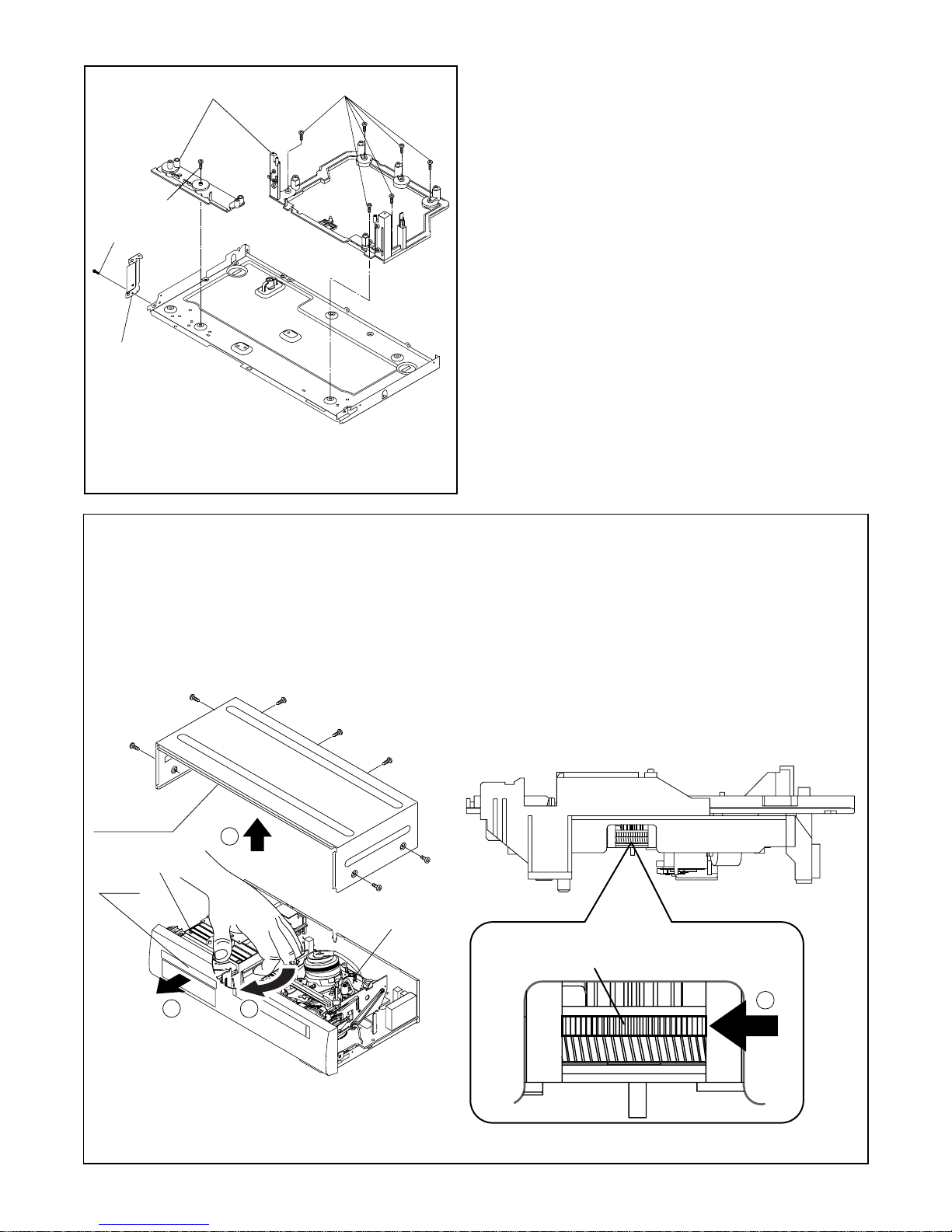
HOW TO MANUAL EJECT
Fig. D9
1. Remove the Top Case.
2. Rotate this roulette in the direction of the arrow as
shown below.
Top Cover
1
VD Mecha
Tray
Deck Assembly
Rotate this roulette in
3
2
the direction of the arrow
2
1-8-5 H9460DC
ELECTRICAL ADJUSTMENT INSTRUCTIONS
e
2
)
C
C
c
General Note: "CBA" is an abbreviation for
"Circuit Board Assembly."
NOTE:
1.Electric al adjust ments are required a fter repla cing
circuit components and ce rtain mechanical par ts.
It is impor tant to do these adjustments only afte r
all repairs and replacements have been completed. Also, do not attempt these adjustments
unless the proper equipment is available.
2.To perform these alignment / confi rmation procedures, make sure that the tracking control is set in
the center position: P ress ei ther "CHA NNEL L5??" or
"CHANNEL K" button on th e front panel first , then
the "PLAY" button on the front panel.
H1
H2
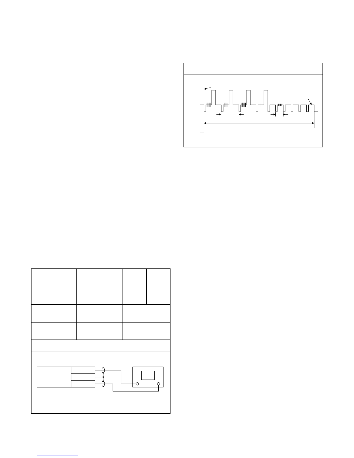
Figure 1
EXT. Syncronize Trigger Point
1.0H
Switching Pulse
6.5H
V-Syn
0.5H
Test Equipment Required
1.Oscilloscope: Dual-trace with 10:1 probe,
V-Range: 0.001~50V/Div.,
F-Range: DC~AC-20MHz
2.Alignment Tape (VFMS0001H6)
Head Switching Po sition Adjustment
Purpose:
To determine the Head Switching point during
playback.
Symptom of Mi sadjustm e n t:
May cause Head Switching noise or ver tical jitter
in the picture.
Test point Adj.Point Mode Input
TP751(V-OUT)
TP302(RF-SW)
GND
Tape
VR501
(Switching Point)
(MAIN CBA)
Measurement
Equipment
PLAY
(SP)
Spec.
Reference Notes:
Playback the Alignment tape and adjust VR501 so that
the V-sync front edge of the CH1 video output waveform is at the 6.5H(412 .7µs) del ayed position from the
rising edge of the CH2 head switching pulse waveform.
-----
VFMS0001H6 Oscilloscope
Connections of Measurement Equipment
TP751
Main CBA
GND
TP302
6.5H±1H
(412.7µs±60µs)
Oscilloscop
CH1 CH
Trig. (+
1-9-1 H9460EA
D
t
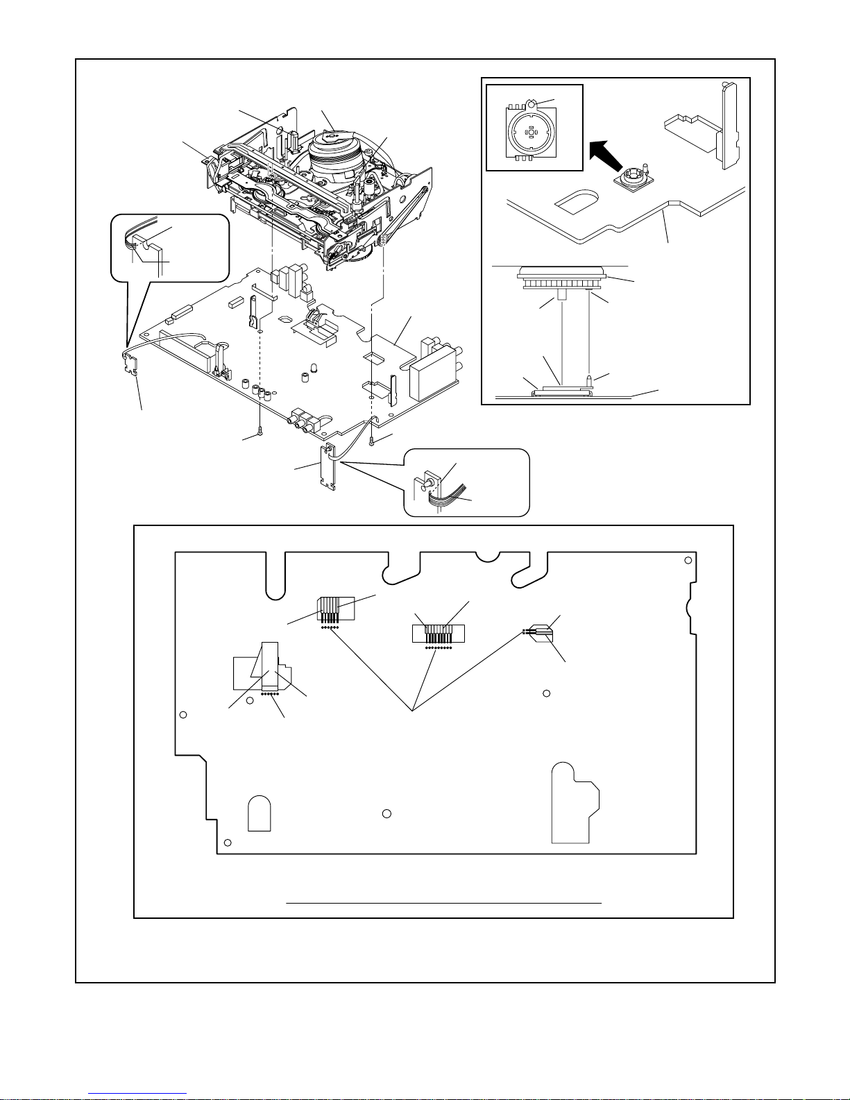
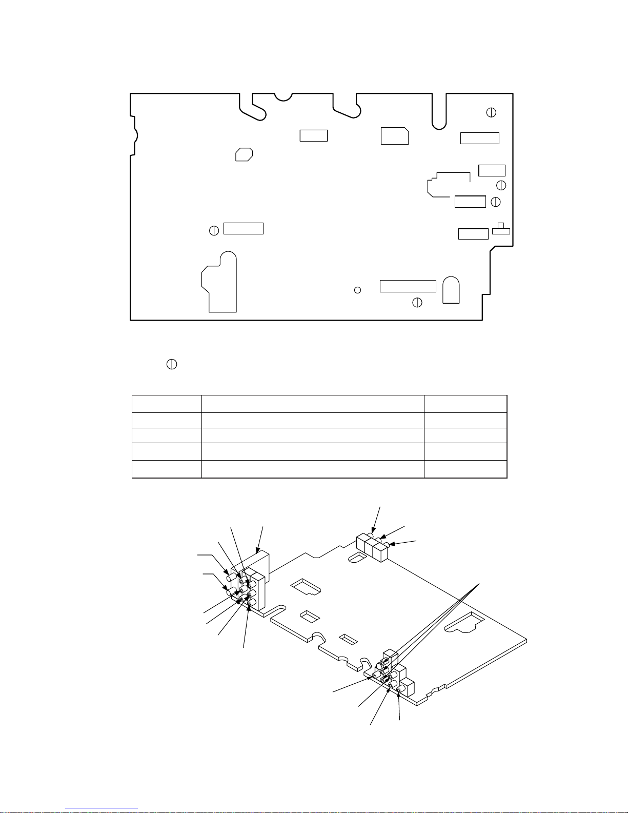
Adjustment Points and Test Points
Main CBA Top View
TP302
RF-SW
TP751
V-OUT
TP513
CTL
TP301
C-PB
VR501
SW-P
TP502
SENS-INH
TEST POINT INFORMATION
: Indicates a test point with a jumper wire across a hole in the PCB.
TEST POINTS NOT USED IN ELECTRICAL ADJUSTMENTS
Test Point
TP301
TP302
TP513
TP502
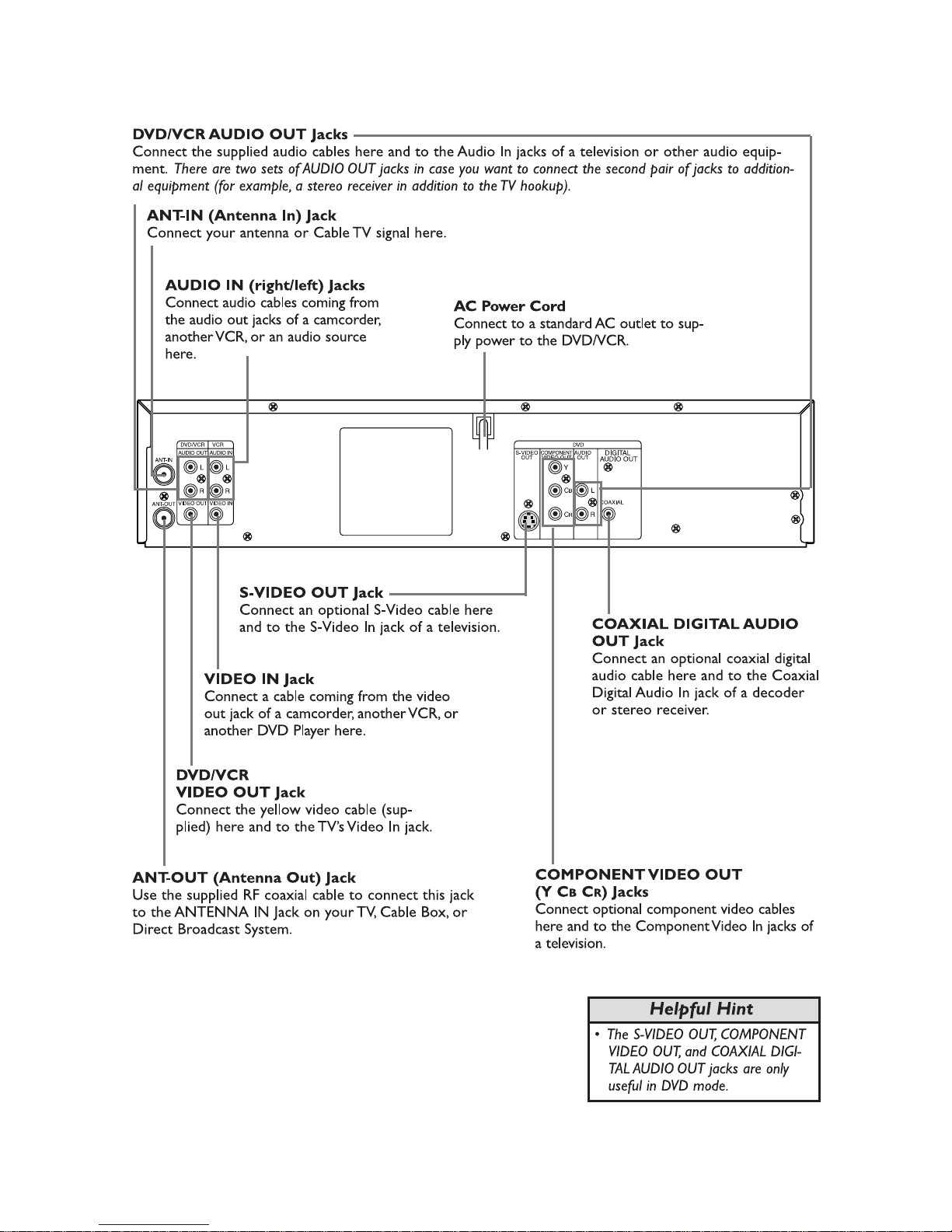
DVD/VCR Audio L In
DVD/VCR Audio L Out
Antenna In
Antenna Out
VD/VCR Audio R Out
DVD/VCR Video Out
DVD/VCR Audio R In
DVD/VCR Video In
Used in: Page No.
Mechanical Alignment Procedures
Mechanical Alignment Procedures
Mechanical Alignment Procedures
Preparation for Servicing
DVD/VCR Audio R In
Tuner Unit
2-3-3, 2-3-4
2-3-3, 2-3-4
2-3-3
1-5-1
DVD/VCR Audio L In
DVD/VCR Video In
Componen
Video Out
S-Video Out
DVD Audio L Out
DVD Audio R Out
1-9-2 H9460EA
Digital Audio Out

FIRMWARE RENEWAL MODE
F
e
F
e)
F
e)
1. Turn the power on and remove the disc on the tray.
2. To put the DVD p layer into version up mode, press
[9], [8], [7], [6], and [SEARCH MO DE] buttons on
the remote control unit in that order. The tray will
open automatically.
Fig. a appears on the screen and Fig. b appears on
the VFD.
F/W Version Up Mode
Please insert a DISC
for F/W Version Up.
EXIT: POWER
Fig. a Version Up Mode Screen
ig. b VFD in Version Up Mod
The DVD player can also enter the version up
mode with the tray open. In this case, Fig. a will be
shown on the screen while the tray is open.
3. Load the disc for version up.
4. The DVD player enters the F/W version up mode
automatically. Fig. c appears on the screen and
Fig. d appears on the VFD.
F/W Version Up Mode
VERSION : ********
Reading...(*2)
5. A fter programming is fini shed, the tray opens au tomatically. Fig. e appears on the screen and the
checksum in (*3) of Fig. e appears on the VFD.
(Fig. f)
F/W Version Up Mode
VERSION : ********
Completed
SUM : 7abc (*3)
Fig. e Completed Program Mode Screen
ig. f VFD upon Finishing the Programming Mode (Exampl
At this time, no buttons are available.
6. Unplug the AC cord from the AC outlet. Then plug it
again.
7. Turn the power on by pressing the power button
and the tray will close.
8. Press [1], [2], [3], [4], and [DISPLAY] buttons on the
remote control unit in that order.
Fig. g appears on the screen.
model: ****** Ver: **** Region: **
1: VFD TEST
2: TT REPEAT PLAY
3: EEPROM CLEAR
4: MEASUREMENT SERVO
5: DISC READ CHECK
6: MECHA CHECK
7: DISC INFO
8: ERROR RATE
EXIT: POWERRETURN: -----
EXIT: POWER
Fig. c Programming Mode Screen
ig. d VFD in Programming Mode (Exampl
The appearance shown in (*2) of Fig. c is
described as follows:
AppearanceNo. State
Reading... Sending files into the memory
1
Erasing... Erasing previous version data
2
Programming...
3 Writing new version data
Fig. g
9. Press [3] button on the remote control unit.
Fig. h appears on the screen.
model: ****** Ver: **** Region: **
TEST 3: EEPROM CLEAR
EEPROM CLEAR: OK
EXIT: POWERRETURN: -----
Fig. h
10.To finish this mode, press [POWER] button.
1-10-1 H9460TEST
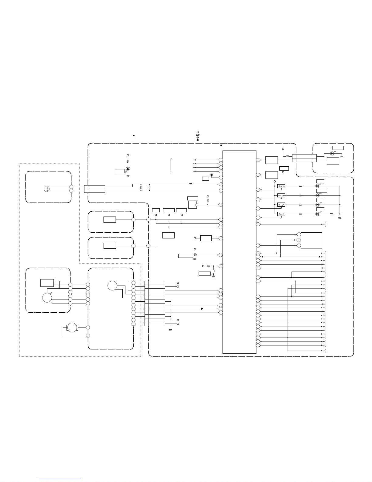
M
M
LOADING
MOTOR
CYLINDER ASSEMBLY
SENSOR CBA
SENSOR CBA
CAPSTAN MOTOR
DRUM
MOTOR
PG
SENSOR
CONTROL
HEAD
CL504
CL502
CN504
AC HEAD ASSEMBLY
MAIN CBA
KEY- 2
RF-SW
C-FG
C-CONT
D-PFG
ST-S
T-REEL
C-F/R
KEY- 1
D-V SYNC
C-SYNC
V-ENV
REMOTE-VIDEO
CTL(+)
RESET
C-ROTA
D-REC-H
D-REC-H
D-PB-L
RECSAF-SW
PG-DELAY
A-MUTE-H
A-MUTE-H
A-MUTE-H
RF-SW
D-V SYNC
C-SYNC
V-ENV
TRICK-H
C-ROTA
END-S
IC501
(SERVO/SYSTEM CONTROL)
5
47
56
CTL
58
CTL(-)
57
28
49
69
62
3
20
27
65
18
78
64
19
41
11
2
24
7
66
67
LM-FWD/REV
21
D-CONT29
(DECK ASSEMBLY)
Servo/System Control Block Diagram
BLOCK DIAGRAMS <VCR SECTION>
END-S
T-REEL
T-REEL
ST-S
ST-S
Q504
Q503
Q501
RESET
Q506
SW-POINT
AL+5V
VR501
TIMER+5V
TP506
TP505
END-S
TP507
D-PB-L
TRICK-H
SP/LP/SLP
14SP/LP/SLP
P-ON-L
22
P-ON-L
P-DOWN-L
1
P-DOWN-L
H-A-SW
79
H-A-SW
H-A-COMP
80
H-A-COMP
46
OUTPUT-SELECT
D-PB-L
D-REC-H
SW511
REC SW
FROM/TO
VIDEO BLOCK
TO AUDIO
BLOCK
FROM/TO
Hi-Fi AUDIO
BLOCK
1-11-1 1-11-2 H9460BLS
CLOCK
DATA
TU701(TUNER UNIT)
23
INSEL/ST-SL
INSEL/ST-SL
16
11
12
VCR/TV5
DVD-IND 71
TIMER-IND 75
REC-IND
72
D567 DVD
D566 VCR
D564 TIMER
POWER
D565
CL508CL509
D561
REC
AL+5V
Q563
Q565
Q566
Q567
LD-SW68
AL+12V
AL+5V
VCR-IND 70
AL+5V
SW512
AL+12V
AL+15V
P-ON+5V
LD-SW
AL+5V
D555
S-LED
FROM/TO POWER
SUPPLY BLOCK
TO DVD SYSTEM
CONTROL BLOCK
DIAGRAM
IIC-BUS SCL
IIC-BUS SDA
12
13IIC-BUS SCL
77
VCR/TV
IIC-BUS SDA
NORMAL-H
ST/SAP-MODE
61
59
Hi-Fi-H-SW
Hi-Fi/NOR-IN
ST/SAP-IN
Hi-Fi-H-SW
25
KEY
SWITCH
KEY
SWITCH
KEY
SWITCH
TP502
P-ON+9V
S-INH
M
CAPSTAN
MOTOR
5 CTL(+)
6 CTL(-)
1 AL+12V
2 P-ON+5V
3 C-FG
4
C-F/R
5
C-CONT
6
GND
7
LM-FWD/REV
8
D-CONT
9
D-PFG
10
GND
11
AL+12V
12
AL+15V
TP513
CTL
OUTPUT-SELECT
OUTPUT-SELECT
OUTPUT-SELECT
DVD-POWER
DVD POWER
26
TO DVD SYSTEM
CONTROL BLOCK
DIAGRAM
<DVD SECTION>
2 2KEY-1
1 1POWER-LED
FUNCTION CBA
FROM/TO DVD SYSTEM
CONTROL BLOCK
DIAGRAM
<DVD SECTION>
REMOTE-VIDEO
DISPLAY-CLK
6
DISPLAY-CLK
DISPLAY-DATA
8
DISPLAY-DATA
DISPLAY-ENA
9
DISPLAY-ENA
" " = SMD
NOTE FOR WIRE CONNECTORS:
1. PREFIX SYMBOL "CN" MEANS CONNECTOR.
(CAN DISCONNECT AND RECONNECT.)
2. PREFIX SYMBOL "CL" MEANS WIRE-SOLDER
HOLES OF THE PCB.
(WIRE IS SOLDERED DIRECTLY.)
TEST POINT INFORMATION
:INDICATES A TEST POINT WITH A JUMPER WIRE ACROSS A HOLE IN THE PCB.
:USED TO INDICATE A TEST POINT WITH A COMPONENT LEAD ON FOIL SIDE.
:USED TO INDICATE A TEST POINT WITH NO TEST PIN.
:USED TO INDICATE A TEST POINT WITH A TEST PIN.

L
R
LUMINANCE
SIGNAL PROCESS
MAIN CBA
Video Block Diagram
VIDEO (R)-1 HEAD
VIDEO (L)-1 HEAD
1-11-3 1-11-4 H9460BLV
(DECK ASSEMBLY)
V(R)-1
V-COM
V(L)-1
CL253
1
2
3
V(L)-2
V-COM
V(R)-2
4
5
6
JK751
V-OUT
Q391
Q760
TU701
VIDEO IN
VCR
DVD
OUTPUT-SELECT
VIDEO OUT
TP751
V-OUT
6
18
JK752
REAR
V-IN
JK753
FRONT
V-IN
V-AGC
TUNER
REAR
IC302 (SW)
FRONT
R P
R
P
SYNC
SEPA
FBC
Y/C
MIX
CCD 1H
DELAY
R
P
DOC YNR Y/C COMB
CHROMINANCE
SIGNAL PROCESS
IC301
(Y/C PROCESS)
REC VIDEO SIGNAL PB VIDEO SIGNAL DVD VIDEO SIGNAL MODE: SP/REC
13
88
89
90
91
42
6dB
AMP
ENV
DET
AGC
AMP
HPF
FROM/TO
SERVO/SYSTEM
CONTROL BLOCK
DIAGRAM
FROM/TO
SERVO/SYSTEM
CONTROL BLOCK
DIAGRAM
CYLINDER ASSEMBLY
R
L
RF-SW
RF-SW
93
V-ENV
H-A-SW
H-A-COMP
H-A-COMP
TP302
WF2
WF1
VIDEO (L)-2 HEAD
VIDEO (R)-2 HEAD
TP301
C-PB
BUFFER
D-V SYNC
C-SYNC
SW CTL
SP/LP/SLP
SP/LP/SLP
C-ROTA
D-V SYNC
C-ROTA
34
14
71
39
59
73
TRICK-H
TRICK
INSEL/ST-SL
INSEL2
74
45 47 49 44
Q301
BUFFER
WF3
40
38
15
94
82
83
84
85
SP
LP/EP
16
D-REC-H
REC/EE/PB
D-PB-L
11
D-REC-H
IC751
(OUTPUT SELECT)
15
1
2
9 10 11
FROM
SERVO/SYSTEM
CONTROL BLOCK
DIAGRAM
DVD-VIDEO
FROM DVD
VIDEO/AUDIO
BLOCK DIAGRAM
<DVD SECTION>
" " = SMD
NOTE FOR WIRE CONNECTORS:
1. PREFIX SYMBOL "CN" MEANS CONNECTOR.
(CAN DISCONNECT AND RECONNECT.)
2. PREFIX SYMBOL "CL" MEANS WIRE-SOLDER
HOLES OF THE PCB.
(WIRE IS SOLDERED DIRECTLY.)
TEST POINT INFORMATION
:INDICATES A TEST POINT WITH A JUMPER WIRE ACROSS A HOLE IN THE PCB.
:USED TO INDICATE A TEST POINT WITH A COMPONENT LEAD ON FOIL SIDE.
:USED TO INDICATE A TEST POINT WITH NO TEST PIN.
:USED TO INDICATE A TEST POINT WITH A TEST PIN.
1
3
7
2
OSD CHARACTER
MIX
38
40
IC501
(OSD)
35

TU701
SIF
Audio Block Diagram
MOD-A
REC
AMP
7
6
AUTO
BIAS
99
P-ON+5V
P-ON+5V
Q421
BIAS
OSC
Q422
Q423 (PB=ON)
Q424
(PB=ON)
Q425
SWITCHING
D-REC OFF
4
EQ
AMP
LINE
AMP
MUTE
96
SP/LP-ON
P
R
ALC
(AUDIO PROCESS) 76
80
78
TUNER
REAR
FRONT
2
15
4 A-PB/REC
CL504
3 A-COM
1 AE-H
2 AE-H/FE-H
AUDIO
HEAD
AUDIO
ERASE
HEAD
AC HEAD ASSEMBLY
FE HEAD
(DECK ASSEMBLY)
1 FE-H
2 FE-H-GND
CL501
1-11-5 1-11-6 H9460BLA
MAIN CBA
PB-AUDIO SIGNAL REC-AUDIO SIGNAL Mode : SP/REC
16
11 12
D-REC-H
D-REC-H
REC/EE/PB
A-MUTE-H
D-PB-L
FROM
SERVO/SYSTEM
CONTROL BLOCK
DIAGRAM
FULL
ERASE
HEAD
IC301
SIF
MOD-A
A-IN (R)-F
A-IN (L)-F
A-IN (L)
A-IN (R)
A-OUT (R)
A-OUT (L)
N-A-OUT
N-A-IN
JK752
A-IN (R)
A-IN (L)
JK754
A-IN (L)-F
JK755
A-IN (R)-F
FROM/TO Hi-Fi AUDIO
BLOCK DIAGRAM
FROM DVD VIDEO/
AUDIO BLOCK
DIAGRAM
<DVD SECTION>
FRONT
REAR
IC751
(OUTPUT SELECT)
DVD-A(L)
DVD-A(R)
98
1
100
2
3
TP753
A-OUT (R)
TP754
A-OUT (L)
SW CTL
DVD
VCR
DVD
VCR
JK751
A-OUT (R)
A-OUT (L)
JK756
A-OUT (R)
A-OUT (L)
9 10 11
5
3
12
13
Q760
14
4
OUTPUT-SELECT
FROM SERVO/SYSTEM
CONTOL BLOCK
DIAGRAM
DVD AUDIO SIGNAL
" " = SMD
NOTE FOR WIRE CONNECTORS:
1. PREFIX SYMBOL "CN" MEANS CONNECTOR.
(CAN DISCONNECT AND RECONNECT.)
2. PREFIX SYMBOL "CL" MEANS WIRE-SOLDER
HOLES OF THE PCB.
(WIRE IS SOLDERED DIRECTLY.)
TEST POINT INFORMATION
:INDICATES A TEST POINT WITH A JUMPER WIRE ACROSS A HOLE IN THE PCB.
:USED TO INDICATE A TEST POINT WITH A COMPONENT LEAD ON FOIL SIDE.
:USED TO INDICATE A TEST POINT WITH NO TEST PIN.
:USED TO INDICATE A TEST POINT WITH A TEST PIN.

57
48 47
13 14
69
74
71
73
6
7
9
12
R-CH
INSEL
L-CH
INSEL
NOR
SW
SERIAL
DATA
DECODER
OUTPUT
SELECT
VCO
LPF
L-CH BPF
R-CH
PNR
PILOT
DET
CONT
STEREO
PLL
STEREO
FILTER
SAP
FILTER
SAP
DET
SIF
DEMOD
SAP
DEMOD
L-R
DEMOD
ST/SAP
SW
MATRIX
L-CH
PNR
LIM DEV
COMP
SW
NOISE
VCO
LPF
LIM DEV
COMP
COMP
DC
SW
NOISE
dBX
DEC
ENV
DET
MODE
OUT
RIPPLE
FILTER
DO
DET
MATRIX
R-CH BPF
P
R
R
L
P
R
HOLD
PULSE
NOISE
DET
ALC
34 33
23
4
80
2
78
37
38
54
77
1
39
26
24
27
SIF
A-IN(R)
A-IN(L)
N-A-OUT
A-IN(R)-F
A-IN(L)-F
DVD-A(L)
DVD-A(R)
LIM
49
MUTE
A-OUT (L)
MOD-A
A-OUT (R)
N-A-IN
Hi-Fi-H-SW
A-MUTE-H
NORMAL-H
40
ST/SAP-MODE
FROM/TO
AUDIO BLOCK
IIC-BUS SDA
IIC-BUS SCL
P-ON+9V
TO SERVO/SYSTEM
CONTROL BLOCK
Hi-Fi
AUDIO
(R) HEAD
Hi-Fi
AUDIO
(L) HEAD
CYLINDER
ASSEMBLY
MAIN CBA
Hi-Fi-A(R) 7
Hi-Fi-COM 8
Hi-Fi-A(L) 9
CL253
IC451 (MTS/ SAP/ Hi-Fi AUDIO PROCESS/ Hi-Fi HEAD AMP)
Hi-Fi Audio Block Diagram
H9460BLH1-11-7 1-11-8
REC-AUDIO SIGNALPB-AUDIO SIGNAL Mode : SP/REC
PILOT
CANCEL
FROM/TO
AUDIO BLOCK
FROM DVD
AUDIO BLOCK
<DVD SECTION>
FROM/TO
SERVO/ SYSTEM
CONTROL BLOCK
FROM
SERVO/SYSTEM
CONTROL BLOCK
62 63
DVD AUDIO SIGNAL
11
" " = SMD
NOTE FOR WIRE CONNECTORS:
1. PREFIX SYMBOL "CN" MEANS CONNECTOR.
(CAN DISCONNECT AND RECONNECT.)
2. PREFIX SYMBOL "CL" MEANS WIRE-SOLDER
HOLES OF THE PCB.
(WIRE IS SOLDERED DIRECTLY.)
TEST POINT INFORMATION
:INDICATES A TEST POINT WITH A JUMPER WIRE ACROSS A HOLE IN THE PCB.
:USED TO INDICATE A TEST POINT WITH A COMPONENT LEAD ON FOIL SIDE.
:USED TO INDICATE A TEST POINT WITH NO TEST PIN.
:USED TO INDICATE A TEST POINT WITH A TEST PIN.

A V
AC1001
F1001
1A 250V
LINE
FILTER
L1001
D1001 - D1004
BRIDGE
RECTIFIER
2
4
Q1001
Q1003
Q1008
8
7
1
23
4
IC1001
ERROR
VOLTAGE DET
HOT
T001
Q055
Q052
Q057
Q056
JUNCTION
CBA
POWER SUPPLY CBA
MAIN CBA
IC1006
(SHUNT REGULATOR)
REG
F
HOT CIRCUIT. BE CAREFUL.
20
19
18
17
16
15
14
13
12
11
Q1006
Q1005
Q1011
1 EV+1.5V
2 EV+1.5V
3 EV+1.5V
4 EV+3.3V
5 EV+3.3V
13 DVD-P-ON+5V
14 EV+9V
15 EV+9V
17 DVD-P-ON+3.3V
19 PWRCON
IC1004
+3.3V REG.
IC1002
+1.5V REG.
CN1001
Q1004
P-ON-L
P-ON+5V
DVD-P-ON+12V
-FL
P-DOWN-L
AL+15V
F2
F1
EV+3.3V
DVD-P-ON+3.3V
AL+33V
P-ON+9V
AL-24V
AL+12V
TIMER+5V
AL+5V
DVD-P-ON+5V
NOTE :
The voltage for parts in hot circuit is measured using
hot GND as a common terminal.
CAUTION
FOR CONTINUED PROTECTION AGAINST FIRE HAZARD,
REPLACE ONLY WITH THE SAME TYPE FUSE.
ATTENTION : POUR UNE PROTECTION CONTINUE LES RISQES
D'INCELE N'UTILISER QUE DES FUSIBLE DE MEMO TYPE.
RISK OF FIRE
-REPLACE FUSE AS MARKED.
"This symbol means fast operating fuse."
"Ce symbole reprèsente un fusible à fusion rapide."
A V
F
1 1AL+44V
2 2P-DOWN-L
3 3AL+12V
5 5AL+5V
7 7AL-24V
1
2
3
5
7
1 1AL+2.35V
3 3AL+4V
6 6F1
7 7F2
CL1004 CN1005
1
2
3
5
7
9
11
14
15
9
11
14
15
CN1003
CN1005 CN1003
CL1002
CL1006 CL1007
TO DVD MAIN
CBA UNIT
CN401
Power Supply Block Diagram
H9460BLP1-11-9 1-11-10
NOTE FOR WIRE CONNECTORS:
1. PREFIX SYMBOL "CN" MEANS CONNECTOR.
(CAN DISCONNECT AND RECONNECT.)
2. PREFIX SYMBOL "CL" MEANS WIRE-SOLDER
HOLES OF THE PCB.
(WIRE IS SOLDERED DIRECTLY.)
CAUTION !
Fixed voltage ( or Auto voltage selectable ) power supply circuit is used in this unit.
If Main Fuse (F001) is blown, check to see that all components in the power supply
circuit are not defective before you connect the AC plug to the AC power supply.
Otherwise it may cause some components in the power supply circuit to fail.

DVD System Control/Servo Block Diagram
H9460BLSD
1-11-11
1-11-12
59
27
7
8
3
15
10
14
26
1
2
3
4
6
23
5
17
18
12
11
14
13
15
16
25
24
FP-STB
55
FP-DIN 54
61
REMOTE-DVD
53
FP-CLK
CN401
CN1001
2
28
1
REMOTE
SENSOR
RM2001
1G
7G
~
~
a
STB
REMOTE-VIDEO
DISPLAY-CLK
DISPLAY-DATA
DISPLAY-ENA
DIN
CLK
GRID
FIP
SEGMENT
FIP502
IC571
DVD MAIN CBA UNIT
MAIN CBA
DRIVE CBA
(FRONT PANEL CONTROL)
IC301
(SERVO DRIVE)
IC451
(CLOCK GENERATOR)
BLOCK DIAGRAMS<DVD SECTION>
16
h
i
IC202
(OP AMP)
12 14
CN3002 CN301
FG CBA
FG
SENSOR
M
SLED
MOTOR
M
SPINDLE
MOTOR
IC101
(MICRO CONTROLLER)
+
-+
-
+
-
+
-
+
-
+
-
+
-
SLED
MOTOR
DRIVE
FOCUS
ACTUATOR
DRIVE
1/4
1/4
PLL2
X451
MULTI
PLL
X'TAL
OSC
36.864MHz
OSC
SPINDLE
MOTOR
DRIVE
TRACKING
ACTUATOR
DRIVE
EXT CLOCK
CLK33M
BE CLOCK
172
170
150
TRAY-OUT
TRAY-IN
FG-IN
97
SLD70
SPDL71
TRACKING
DRIVE
152
FOCUS DRIVE
60
66
TO
DVD VIDEO/ AUDIO
BLOCK DIAGRAM
51
ADAC-MD
50 ADAC-MC
96 ADAC-ML
ADAC-MC
ADAC-ML
PCM-SCLK
95
DVD-A-MUTE
ADAC-MD
DVD-A-MUTE
1792FSEL
RESET68
RESET
IC461
5 4
+3.3V
TRAY-OUT
TRAY-IN
FOCUS SERVO SIGNAL TRACKING SERVO SIGNAL
SLED SERVO SIGNAL SPINDLE SERVO SIGNAL
3SP(+)
4SP(-)
5TRAY-OUT
6TRAY-IN
7GND
8SL(-)
9SL(+)
1FG-IN
FROM/TO SERVO
/SYSTEM CONTROL
BLOCK DIAGRAM
<VCR SECTION>
DVD-POWER
OUTPUT-SELECT
FROM SERVO
/SYSTEM CONTROL
BLOCK DIAGRAM
<VCR SECTION>
CN302
CN2001
CL2002
CL2003
PLAY
STOP
POWER
OPEN
/CLOSE
Q2001
SW2001
DVD
OPEN
/CLOSE
DVD
OPEN/CLOSE CBA
SW2002
STOP
SW2003
PLAY
48
47
62
94
FS(+) 18
FS(-) 19
TS(+) 20
TS(-) 17
CN201
FSTS
PICK-UP
UNIT
FP-STB
1616
FP-DIN 1818
FP-CLK
2121
REMOTE-DVD 2222
PLAY 11
OPEN/CLOSE
22
STOP 22
POWER 33
OPEN/CLOSE 44
OUT-SEL
2020
23
17
~
7
14
~
OUT-SEL
" " = SMD
NOTE FOR WIRE CONNECTORS:
1. PREFIX SYMBOL "CN" MEANS CONNECTOR.
(CAN DISCONNECT AND RECONNECT.)
2. PREFIX SYMBOL "CL" MEANS WIRE-SOLDER
HOLES OF THE PCB.
(WIRE IS SOLDERED DIRECTLY.)

Digital Signal Process Block Diagram
H9460BLD
1-11-14
C 6
D 7
A 8
B 5
F 10
E 2
DVD-LD 14
CD-LD 12
PD-MONI 13
CN201
CN201
IC201
(SW)
IC105 (LATCH)
IC102 (SDRAM) IC101 (MICRO CONTROLLER)
CD/DVD
PICK UP
UNIT
DETECTOR
CD/DVD 9
Q251,Q252
CD DVD
AMP
Q253,Q254
AMP
4
1 3
6
GND(DVD-PD)
15
GND(CD-PD)
16
GND(LD)
11
RF
SIGNAL
PROCESS
CIRCUIT
DVD/CD
FORMATTER
AUDIO
I/F
VIDEO
I/F
NTSC/PAL
ENCODER
DMA
BCU
INST.
ROM
32BIT
CPU
DATA
ROM
INTERRUPT
CONTROLLER
WATCH DOG
TIMER
CPU
I/F
TIMER
DECODER
I/F
CPU
I/F
READ
MEMORY
DATA
ROM
DSP
DECODER
PIXEL
OPERATION
I/O
PROCESSOR
INST.
ROM
DATA
ROM
INST.
ROM
DATA
ROM
INST.
ROM
SERIAL
D/A
GENERAL
I/O
INTERRUPT
CONTROLLER
TIMER
WATCH DOG
TIMER
32BIT CPU
STREAM
I/F
EXTERNAL
MEMORY
I/F
SDRAM
ECC
UMAC
124
125
122
123
128
129
126
127
131
130
133
132
134
78
DEBUG
BCU
INST
CACHE
D TYPE
LATCH
DATA
CACHE
D/A
D/A
D/A
TO DVD
VIDEO
/AUDIO
BLOCK
DIAGRAM
158
164
Y
C
Cr
Cb
VIDEO-Y
VIDEO-C
VIDEO-Cr
VIDEO-Cb
TO DVD
VIDEO
/AUDIO
BLOCK
DIAGRAM
181
SPDIF
175
PCM-BCK
176
PCM-DATA0
174
PCM-LRCLK
161
160
EXT ADT (0-15), EXT ADR (16-19)
EXT ADT (0-15), EXT ADR (16-19)
EXT ADT (0-7)
EXT ADT (8-15)
EXT ADR (0-7)
EXT ADR (0-15)
EXT ADR (8-15)
SDRAM DATA(0-31)SDRAM DATA(0-31)
SDRAM ADDRESS(0-10)SDRAM ADDRESS(0-10)
2
9
~
12
19
~
210
235
~
IC104 (LATCH)
D TYPE
LATCH
2
9
~
12
19
~
2
13
184
205
247
256
~~~
2
13
31
56
74
85
~~~
IC103 (FLASH ROM)
FLASH
ROM
29
36
38
45
~~
DVD MAIN CBA UNIT
DATA(VIDEO/AUDIO) SIGNAL DVD VIDEO SIGNAL
DATA(AUDIO) SIGNAL
24
27
60
66
~~
EXT ADT (0-15)
EXT ADR (16-19)
~
1
9
16
25
48
~
135
1-11-13
" " = SMD

DVD Video / Audio Block Diagram
H9460BLVD
1-11-15 1-11-16
IC601 (AUDIO DAC)
7
8
12
11
DIGITAL
AUDIO OUT
JK1202
AMP
Q1351
IC1201
Q1203
Q1201
Q1202
VREF
+3.3V
(AMP)
CN601 CN1601
11 11DVD-A(L)
1313DVD-A(R)
12 12
DVD-A(L)-MUTE
14 14
DVD-A(R)-MUTE
10 10
DVD-A-MUTE
1
2
3
13
14
15
16
FROM
DVD
SYSTEM
CONTROL
/SERVO
BLOCK
DIAGRAM
FROM
DIGITAL
SIGNAL
PROCESS
BLOCK
DIAGRAM
SERIAL
PORT
SERIAL
CONTROL
4X/8X
OVERSAMPLING
DIGITAL FILTER
/FUNCTION
CONTROLLER
ENPHANCED
MULTI-LEVEL
DELTA-SIGMA
MODULATOR
DAC
LPF+AMP
L-CH
R-CH
LPF+AMP
DAC
ZERO DETECT
SYSTEM CLOCK
1
2
6
7
5
DVD-A(L)
DVD-A(R)
PCM-BCK
SPDIF
PCM-DATA0
PCM-LRCLK
ADAC-MD
ADAC-MC
ADAC-ML
PCM-SCLK
MAIN CBADVD MAIN CBA UNIT
DVD AUDIO SIGNALDATA(AUDIO) SIGNAL
1616SPDIF
A-MUTE
+3.3V
Q1204
WF9
3
WF7
WF8
CN601
5 5VIDEO-Y
7 7VIDEO-C
3 3VIDEO-Cb
1 1VIDEO-Cr
VIDEO-Y
VIDEO-C
VIDEO-Cb
VIDEO-Cr
JK1401
S-VIDEO OUT
CN1601
3 4
2
1
IC1402 (VIDEO DRIVER)
18
4dB
AMP
2dB
AMP
LPF DRIVER
Y
C
21
2dB
AMP
DRIVER
4dB
AMP
2dB
AMP
LPF DRIVER
15
4dB
AMP
2dB
AMP
LPF DRIVER
9
13
4dB
AMP
2dB
AMP
LPF DRIVER
11
VIDEO-Cb
OUT
VIDEO-Y
OUT
VIDEO-Cr
OUT
JK1403
6
2
23
FROM DIGITAL
SIGNAL PROCESS
BLOCK DIAGRAM
DVD VIDEO SIGNAL
WF4
WF5
WF6
TO
Hi-Fi AUDIO
BLOCK
DIAGRAM
<VCR
SECTION>
DVD-VIDEO TO VIDEO
BLOCK DIAGRAM
<VCR SECTION>
" " = SMD

SCHEMATIC DIAGRAMS / CBA’S AND TEST POINTS
1
T
b
ts
<
>
(
or
Standard Notes
Notes:
1. D o not use the par t number shown on these draw-
WARNING
Critical comp onents having sp ecial safety characte ristics are identified with a # by the Ref. No. in the parts
list and enclosed w ithin a broken line (where several
critical components are grouped in one area) along
with the safety symbol # on the schematics or
exploded views.
Use of substitute replacement parts which do not have
the same specified safety characteristics may create
shock, fire or other hazards.
Under no circumstances s hould the ori ginal desi gn be
modified or altered without written permission from
Philips Consumer Electronics Company. Philips
assumes no lia bility, express or implied, arising ou t of
any unauthorized modification of design. Servicer
assumes all liability.
* Broken Line :
Capacitor Temperature Markings
Mark
(B)
Capacity
change rate
±10%
Standard
Temperature
temperature
20°C -25~+85°C
range
ings for ordering. The correct part number is shown
in the parts list, and may be slightly different or
amended since these drawings were prepared.
2. To maintain original function and reliability of
repaired units, use only original replacem ent parts
which are listed with their part numbers in the parts
list section of the service manual.
3. Prefix symbol "CN" means "connector" (can disconnect and reconnect).
Prefix symbol "CL" m ean s " wir e-s old er hol es of the
PCB" (wire is soldered directly).
4. How to read converged lines.
-D3
Distinction Area
Line Number
(1 to 3 digits)
3
AREA D3
2
1
AREA B1
1-D3
ABCD
1-B1
Examples:
(1)."1-D3" means that line number "1" goes to area
"D3."
(2)."1-B1" means that line number "1" goes to area
"B1."
5. All resistance values are indicated in ohms
(F) +30 - 80% 20°C –25~+85°C
(SR)
±15%
20°C –25~+85°C
6. Resistor wattages are 1/4W or 1/6W unless other-
(K=10
3
, M=106).
wise specified.
(Z)
±22.5%
Capacitors and transistor s are represent ed by the following symbols.
20°C –25~+85°C
7. All capacitance values are indicated in µF
-6
(P=10
µF).
8. All voltages are DC voltages unless otherwise
specified.
9. Voltage indications PLAY and REC modes on the
schematics are as shown below.
< PCB Symbols >
(Top View) (Bottom View)
+
Electrolytic Capacitor
Bottom View)
Transistor or Digital Transistor
E C B
(Top View)
NPN Transistor
E C B
(Top View)
NPN Digital Transistor
E C B
(Top View)
(Top View)
PNP Transist
E C B
PNP Digital
Transistor
E C B
he same voltage for
oth PLAY & STOP modes
The same voltage for
both PLAY, REC & DVD
modes
< DVD Section >
231
5.0
<
VCR Section >
5.0
Schematic Diagram Symbols
Digital Transistor
5.0
(2.5)
Indicates that the voltage
is not consistent here.
231
5.0
(2.5)
< >
Indicates that the voltage
is not consistent here.
Unit: Vol
PLAY mode
STOP mode
PLAY mode
REC mode
DVD mode
1-12-1 SC_01

S
Main 1/8 Schematic Diagram Parts Location Guide
Ref No. Position Ref No. Position
CAPACITORS
C023 E-4 R503 D-1
C502 B-1 R504 D-1
C505 D-1 R507 D-3
C507 D-1 R508 D-3
C508 D-3 R511 E-4
C509 E-3 R517 E-4
C511 D-3 R518 E-4
C512 D-3 R521 C-4
C514 D-3 R523 D-4
C515 D-3 R524 C-4
C521 E-3 R525 B-3
C522 E-4 R526 B-4
C523 C-4 R527 B-3
C525 C-4 R528 B-3
C527 E-4 R529 E-1
C529 D-4 R530 B-2
C530 D-4 R537 A-3
C531 C-4 R542 A-1
C532 C-4 R543 A-2
C533 C-4 R544 B-4
C534 C-4 R545 C-2
C535 C-4 R546 C-2
C536 C-4 R551 D-2
C537 B-4 R610 C-1
CONNECTORS
CL501 A-4 R 614 D-2
CL502 F-4 R616 D-4
CL504 A-4 R 618 B-2
DIODES
D501 E-4 R626 C-1
D510 F-3 R640 E-2
D555 A-1
ICS
IC501 C-3
COILS
L501 A-1
L502 E-3 X501 D-3
TRANSISTORS
Q501 D-1
Q506 A-3 TP505 B-3
RESISTORS
R502 D-1
RESISTORS
R611 D-2
R619 B-2
SWITCHES
SW511 A-2
VARIABLE RESISTORS
VR501 B-4
CRYSTAL OSCILLATOR
X502 D-3
TEST PO I NTS
TP513 B-4
1-12-2

Main 1/8 Schematic Diagram < VCR Section >
1-12-3
1-12-4
H9460SCM1
“ “ = SMD
THE SAME VOLTAGE FOR BOTH
PLAY , REC & D VD MODES.
INDICATES THA T THE VOL TAGE
IS NOT CONSISTENT HERE.
PLAY MODE
REC MODE
1
2
3
5.0
5.0
(2.5)
<5.0>
~
DVD MODE
IC501 KEY VOLTAGE CHART
KEY 1 (67PIN) KEY 2 (66 PIN)
0.00 ~ 0.51V REW OUTPUT
0.51 ~ 0.92V POWER STOP/EJECT
0.92 ~ 1. 27V - ---- ------ PLAY
1.27 ~ 1. 61V - ---- ---- -- -----------
1.61 ~ 1. 98V - ---- ---- -- -----------
1.98 ~ 2. 39V - ---- ------ S-INH
2.39 ~ 2. 90V - ---- ---- -- -----------
2.90 ~ 3. 60V - ---- ---- -- -----------
3.60 ~ 4. 30V - ---- ---- -- -----------
4.30 ~ 5.00V KEY OFF KEY OFF
Pin No.
Voltage

Main 2/8 Schematic Diagram < VCR Section >
1-12-5
1-12-6
H9460SCM2
“ “ = SMD
THE SAME VOLTAGE FOR BOTH
PLAY , REC & D VD MODES.
INDICATES THA T THE VOL TAGE
IS NOT CONSISTENT HERE.
PLAY MODE
REC MODE
1
2
3
5.0
5.0
(2.5)
<5.0>
~
DVD MODE

Main 2/8 Schematic Diagram Parts Location Guide
Ref No. Position Ref No. Position
CAPACITORS RESISTORS
C540 K-1 R566 H-3
C550 J-4 R567 H-3
C571 K-2 R568 H-3
C572 K-2 R570 I-3
C574 K-2 R571 J-3
C701 I-1 R572 K-3
C703I-1R573I-3
C704 H-1 R574 I-3
C708 H-1 R575 I-3
C709 H-1 R576 I-3
CONNECTORS
CL509 G-4 R590 I-4
DIODES
D502 H-3 R594 H-4
D564 H-2 R600 G-3
D565 H-2 R602 G-3
D566 I-2 R603 G-3
D567 I-2 R605 G-3
ICS
IC571 J-3 R704 H-1
COILS
L701 H-1 R706 H-1
TRANSISTORS
Q503 L-1 R2033 G-3
Q504 L-1 R2041 G-3
Q563 H-3 R2042 H-3
Q565 H-3
Q566 I-3 SW502 H-4
Q567 I-3 SW503 I-4
RESISTORS
R467 I-1 SW505 H-4
R531 K-2 SW512 J-1
R532 J-2
R533 J-2FIP502J-4
R534 J-2 TU701 H-2
R535 J-2
R536 J-2 TP502 I-4
R540 K-2 TP506 K-1
R541 K-2 TP507 K-1
R561 H-4
R583 I-4
R593 H-4
R701 H-1
R705 H-1
R2025 G-3
SWITCHES
SW504 I-4
MISCELLANEOUS
TEST PO I NTS
1-12-7

Main 3/8 Schematic Diagram Parts Location Guide
S
Ref No. Position Ref No. Position Ref No. Position
RESISTORSCAPACITORS CAPACITORS
C253 N-2 C409 N-2 R323 R-3
C255 N-2 C410 N-2 R324 R-3
C256 N-4 C411 N-1 R326 Q-3
C257 N-4 C413 O-1 R327 Q-4
C308 P-1 C415 O-1 R328 P-4
C309 P-1 C417 O-1 R329 Q-4
C310 O-1 C418 O-1 R331 P-4
C311 P-2 C419 O-1 R332 P-4
C312 Q-1 C421 N-1 R341 P-1
C314 Q-1 C422 N-1 R342 P-1
C315 Q-1 C423 N-1 R343 Q-4
C320 Q-2 C424 N-1 R357 Q-2
C321 Q-2 C425 M-1 R370 Q-1
C322 Q-2 R371 R-1
C324 Q-3 CL253 M-4 R391 Q-1
C325 Q-3 R392 Q-1
C326 Q-3 IC301 N-2 R395 P-1
C328 Q-4 IC302 Q-2 R397 P-1
C329 Q-4 R401 O-4
C330 Q-4 L251 N-4 R402 O-4
C331 Q-4 L303 N-4 R407 O-4
C332 P-4 L304 N-4 R408 N-2
C333 P-4 L421 N-1 R409 N-2
C335 P-4 L422 M-1 R410 N-2
C336 P-4 R411 N-2
C337 P-4 Q301 Q-3 R412 N-2
C339 P-4 Q302 Q-4 R413 N-2
C340 P-4 Q391 P-1 R414 O-1
C341 O-4 Q421 N-1 R415 O-1
C344 P-4 Q422 N-1 R416 O-1
C345 P-4 Q423 N-1 R417 O-1
C346 P-4 Q424 N-1 R418 O-1
C347 P-4 Q425 N-1 R419 O-1
C348 O-4 R421 N-2
C349 O-4 JC02 O-1 R422 N-1
C352 Q-3 JC03 O-1 R424 N-1
C353 P-4 R253 N-2 R425 N-1
C354 Q-3 R254 N-2 R426 N-1
C370 Q-1 R303 O-1 R428 N-1
C371 Q-1 R304 P-1 R429 N-1
C391 Q-1 R305 P-1 R430 O-4
C392 Q-1 R306 P-1 R431 N-4
C401 O-4 R309 P-1
C404 O-4 R311 P-1 X301 P-4
C405 N-4 R312 Q-1
C406 O-4 R313 Q-1 TP301 O-1
C408 N-2 R322 Q-3 TP302 P-1
CONNECTORS
ICS
COILS
TRANSISTORS
RESISTORS
CRYSTAL OSCILLATOR
TEST PO I NTS
1-12-8

“ “ = SMD
1-12-9
1-12-10
H9460SCM3
Main 3/8 Schematic Diagram < VCR Section >
THE SAME VOLTAGE FOR BOTH
PLAY , REC & D VD MODES.
INDICATES THA T THE VOL TAGE
IS NOT CONSISTENT HERE.
PLAY MODE
REC MODE
1
2
3
5.0
5.0
(2.5)
<5.0>
~
DVD MODE

Main 4/8 Schematic Diagram < VCR Section >
1-12-11
1-12-12
H9460SCM4
“ “ = SMD
THE SAME VOLTAGE FOR BOTH
PLAY , REC & D VD MODES.
INDICATES THA T THE VOL TAGE
IS NOT CONSISTENT HERE.
PLAY MODE
REC MODE
1
2
3
5.0
5.0
(2.5)
<5.0>
~
DVD MODE

Main 4/8 Schematic Diagram Parts Location Guide
Ref No. Position Ref No. Position
CAPACITORS
C438 S-3 C489 S-3
C439 U-2 C491 S-3
C440 S-3 C492 S-3
C441 U-2 C493 S-3
C448 T-2 C494 S-3
C449 T-2 C495 T-4
C451 T-1 C496 S-3
C452 T-2 C498 S-2
C453 T-2 C499 S-2
C454 U-2
C455 U-2 IC451 S-2
C456 U-2
C457 U-2 L451 V-3
C458 U-2
C459 V-2 R451 T-2
C460 V-2 R452 T-2
C461 V-2 R455 T-2
C462 V-2 R456 T-2
C463 V-3 R457 V-2
C465 V-3 R458 V-3
C466 V-3 R459 V-3
C467 V-3 R462 T-4
C470 V-4 R463 S-3
C471 U-4 R464 S-3
C472 U-4 R468 S-2
C473 U-4 R469 S-2
C474 U-4 R470 S-2
C475 U-4 R471 S-2
C476 U-4 R472 V-3
C477 T-4 R480 S-3
C478 T-4 R481 S-2
C479 T-4 R482 U-1
C480 T-4 R483 U-1
C481 T-4 R484 S-3
C483 T-4 R485 S-2
C484 T-4 R486 U-2
C485 T-4 R487 U-2
C486 T-4
C487 S-4 TP452 V-3
C488 T-3
CAPACITORS
ICS
COILS
RESISTORS
TEST PO I NTS
1-12-13

Main 5/8 Schematic Diagram Parts Location Guide
Ref No. Position Ref No. Position Ref No. Position
CAPACITORS
C1201 X-1 D1301 Y-2 R1233 X-2
C1202 X-1 R1235 Y-1
C1205 Y-1 IC1201 Y-1 R1236 Y-1
C1206 Y-1 IC1402 Z-3 R1237 Y-1
C1207 Y-1 R1238 Y-1
C1208 Y-1 L1350 Z-2 R1239 Y-1
C1221 Y-1 L1351 BB-1 R1240 Y-1
C1222 Y-1 L1401 AA-2 R1245 Y-1
C1223 Z-1 L1441 AA-2 R1351 AA-1
C1224 Z-1 L1442 AA-2 R1352 AA-1
C1245 Y-1 L1461 AA-2 R1353 AA-1
C1246 X-1 L1481 AA-2 R1354 AA-1
C1247 Y-1 L1521 Y-2 R1355 AA-1
C1249 Y-1 R1356 BB-1
C1350 AA-1 Q1201 Z-1 R1371 X-2
C1351 AA-2 Q1202 Z-1 R1392 X-2
C1353 AA-1 Q1203 Z-1 R1396 Y-2
C1354 AA-1 Q1204 Z-1 R1397 Y-2
C1355 Z-1 Q1351 AA-1 R1402 AA-3
C1358 AA-1 Q1385 Y-2 R1421 Y-2
C1394 Y-2 R1422 AA-2
C1395 Y-2 R1203 X-1 R1441 Y-3
C1402 AA-3 R1204 X-1 R1442 AA-2
C1421 Y-3 R1205 X-1 R1443 AA-2
C1422 AA-2 R1206 Y-1 R1461 Y-3
C1441 Y-3 R1207 Y-1 R1462 AA-2
C1442 AA-2 R1208 Y-1 R1481 Y-3
C1461 Y-3 R1209 Y-1 R1482 AA-2
C1462 AA-2 R1210 Y-1 R1612 Y-2
C1481 Y-3 R1211 Y-1
C1482 AA-2 R1212 Y-1 JK1202 BB-1
C1523 Y-3 R1221 Y-1 JK1401 AA-2
C1524 Z-3 R1222 Y-1 JK1403 AA-2
C1531 Y-2 R1223 Z-1
C1532 Y-2 R1224 Z-1
CONNECTORS
CN1601 X-3 R 1226 Z-1
DIODES
ICS
COILS
TRANSISTORS
RESISTORS
R1225 Z-1
RESISTORS
MISCELLANEOUS
1-12-14

Main 5/8 Schematic Diagram < VCR Section >
1-12-15
1-12-16
H9460SCM5
“ “ = SMD
THE SAME VOLTAGE FOR BOTH
PLAY , REC & D VD MODES.
INDICATES THA T THE VOL TAGE
IS NOT CONSISTENT HERE.
PLAY MODE
REC MODE
1
2
3
5.0
5.0
(2.5)
<5.0>
~
DVD MODE

Main 6/8 Schematic Diagram < VCR Section >
1-12-17
1-12-18
H9460SCM6
MAIN 6/ 8 S c hematic Diagram
Parts Location G uide
Ref No. Position
C751 EE-2
C752 FF-2
C762 DD-3
C766 EE-3
C772 EE-2
C773 EE-2
C777 EE-3
D702 CC-4
IC751 DD-4
Q760 CC-3
R453 DD-1
R454 DD-1
R465 DD-1
R466 DD-1
R751 EE-2
R752 EE-1
R753 EE-1
R777 EE-3
R778 EE-3
R779 EE-4
R780 DD-4
JK751 FF-2
JK752 FF-1
JK753 FF-1
JK754 FF-1
JK755 FF-1
JK756 FF-2
TP751 EE-2
TP753 EE-2
TP754 EE-2
TEST POINTS
CAPACITORS
DIODES
RESISTORS
ICS
TRANSISTORS
MISCELLANEOUS
“ “ = SMD
THE SAME VOLTAGE FOR BOTH
PLAY , REC & D VD MODES.
INDICATES THA T THE VOL TAGE
IS NOT CONSISTENT HERE.
PLAY MODE
REC MODE
1
2
3
5.0
5.0
(2.5)
<5.0>
~
DVD MODE

Main 7/8 Schematic Diagram < VCR Section >
1-12-19
1-12-20
H9460SCM7
MAIN 7/8 Schem a tic Diagram
Parts Location Guide
Ref No. Position
C2002 JJ-2
C2004 KK-1
C2012 KK-1
CL2002 GG-4
CL2003 GG-4
CN2001 GG-3
D2010 JJ-2
L2001 KK-2
Q2001 II-2
R2001 II-3
R2002 II-3
R2003 II-3
R2005 KK-2
R2006 II-3
R2028 KK-2
R2031 JJ-2
R2062 II-2
R2064 II-2
SW2001 GG-4
SW2002 II-2
SW2003 II-2
RM2001 KK-2
RESISTORS
SWITCHES
MISCELLANEOUS
CAPACITORS
CONNECTORS
DIODES
COILS
TRANSISTORS
“ “ = SMD
THE SAME VOLTAGE FOR BOTH
PLAY , REC & D VD MODES.
INDICATES THA T THE VOL TAGE
IS NOT CONSISTENT HERE.
PLAY MODE
REC MODE
1
2
3
5.0
5.0
(2.5)
<5.0>
~
DVD MODE

Main 8/8 Schematic Diagram < VCR Section >
1-12-21
1-12-22
H9460SCM8
“ “ = SMD
THE SAME VOLTAGE FOR BOTH
PLAY , REC & D VD MODES.
INDICATES THA T THE VOL TAGE
IS NOT CONSISTENT HERE.
PLAY MODE
REC MODE
1
2
3
5.0
5.0
(2.5)
<5.0>
~
DVD MODE

Main 8/8 Schematic Diagram Parts Location Guide
Ref No. Position Ref No. Position
CAPACITORS
C051 PP-3 Q056 QQ-3
C053 PP-3 Q057 PP-3
C060 PP-3 Q1004 PP-1
C1015 MM-4 Q1005 NN-2
C1038 OO-1 Q1006 OO-2
C1039 NN-3 Q1011 NN-1
C1040 NN-3
C1042 MM-1 R056 PP-4
C1070 MM-3 R057 QQ-3
C1071 NN-2 R058 PP-3
CONNECTORS
CN1001 MM-3 R 061 PP-3
CN1003 MM-4 R 062 PP-3
DIODES
D019 PP-3 R073 QQ-4
D052 PP-3 R075 QQ-4
D071 PP-3 R087 QQ-4
D080 PP-3 R088 QQ-4
D081 PP-3 R090 OO-3
D100 OO-1 R091 OO-3
D101 OO-1 R702 QQ-4
D701 QQ-4 R1002 NN-3
D1030 OO-1 R1013 NN-4
D1035 NN-3 R1025 NN-2
D1036 NN-3 R1040 MM-4
D1037 NN-3 R1042 MM-4
D1038 NN-3 R1044 NN-2
D1040 OO-2 R1059 MM-2
D1041 OO-2 R1068 PP-1
D1058 PP-1 R1076 N N-2
ICS
IC1002 NN-3 R1078 NN-3
IC1004 OO-1 R1080 QQ-1
COILS
L1009 OO-1 R1086 NN-3
L1010 OO-2 R1090 NN-1
TRANSISTORS
Q052 QQ-4 R2050 MM-1
Q055 PP-3 R2060 MM-1
TRANSISTORS
RESISTORS
R060 OO-3
R063 PP-3
R1077 PP-1
R1085 NN-3
R1091 NN-1
1-12-23

Function Schematic Diagram < VCR Section >
1
Note:
*
When it is necessary to replace one or more of the following Diodes,
all one should be replaced: D561.
FUNCT ION Schematic Diagram
Par t s Loc at ion Guide
Ref No. Position
CONNECTORS
CL508 A-1
DIODES
D561 B-1
RESISTORS
R584 B-2
SWITCHES
SW501 B-1
H9460SCF
1-12-24

SW-P
VR501
CTL
TP513
RF-SW
TP302
WF2
C-PB
TP301
WF3
V-OUT
TP751
WF1
S-INH
TP502
1-12-25 1-12-26
Main CBA Top View
BH9400F01013A
BHB300F01014-A
BHB300F01014-B
Sensor CBA Top View

1-12-27
Main CBA Bottom View
BH9400F01013A
1-12-28

1-12-29 1-12-30
Main CBA Parts Location Guide
Ref No. Position Ref No. Position Ref No. Position Ref No. Position Ref No. Position
Q1201 A-4 R412 C-3 R528 D-1 R1025 A-3 R2001 A-1
Q1202 A-4 R413 C-3 R529 D-3 R1040 A-1 R2002 A-1
Q1203 A-3 R414 C-3 R530 C-1 R1042 A-4 R2003 A-1
Q1204 A-2 R415 C-3 R531 D-1 R1044 A-3 R2005 B-1
Q1351 A-4 R416 D-3 R532 E-1 R1059 B-2 R2006 A-1
Q1385 A-2 R417 D-3 R533 E-2 R1068 A-3 R2025 A-1
Q2001 A-1 R418 D-3 R534 E-2 R1076 B-2 R2028 B-1
R419 D-3 R535 E-2 R1077 A-3 R2031 B-1
JC02 C-3 R421 C-4 R536 E-2 R1078 B-1 R2033 A-1
JC03 B-3 R422 C-4 R537 C-1 R1080 B-2 R2041 A-1
R056 C-4 R424 C-3 R540 D-1 R1085 B-4 R2042 A-1
R057 C-4 R425 B-3 R541 B-1 R1086 B-4 R2050 A-2
R058 E-3 R426 D-3 R542 C-2 R1090 A-4 R2060 A-1
R060 C-4 R428 C-4 R543 B-1 R1091 A-4 R2062 A-1
R061 C-4 R429 C-4 R544 E-2 R1203 A-3 R2064 A-1
R062 C-4 R430 C-3 R545 C-1 R1204 A-3
R063 C-4 R431 C-3 R546 C-1 R1205 A-3 SW502 C-1
R073 C-4 R451 B-3 R551 C-2 R1206 A-3 SW503 D-1
R075 C-4 R452 B-3 R561 E-1 R120 7 A-3 SW504 D-1
R087 E-3 R453 B-3 R566 C-1 R1208 A-3 SW505 C-1
R088 E-3 R454 B-3 R567 C-1 R1209 A-3 SW511 B-1
R090 D-3 R455 B-3 R568 C-1 R1210 A-3 SW512 E-1
R091 D-3 R456 B-3 R570 C-1 R1211 A-3 SW2002 A-1
R253 C-3 R457 B-3 R571 A-1 R121 2 A-3 SW2003 A-1
R254 C-3 R458 C-3 R572 A-1 R1221 A-3
R303 D-3 R459 C-3 R573 C-1 R1222 A-3 VR501 E-2
R304 D-3 R462 B-2 R574 C-1 R1223 A-3
R305 D-3 R463 B-2 R575 C-1 R1224 A-3 X301 C-3
R306 D-3 R464 B-2 R576 C-1 R1225 A-4 X501 D-2
R309 D-3 R465 B-2 R583 D-1 R1226 A-4 X502 D-1
R311 D-3 R466 B-2 R590 D-1 R1233 A-3
R312 D-3 R467 B-4 R593 C-1 R1235 A-2 FIP502 B-1
R313 C-3 R468 B-3 R594 C-1 R1236 A-2 JK751 E-4
R322 C-2 R469 B-3 R600 A-1 R1237 A-3 JK752 E-4
R323 C-2 R470 B-3 R602 B-2 R1238 A-2 JK753 D-1
R324 C-2 R471 B-3 R603 B-1 R1239 A-2 JK754 E-1
R326 C-2 R472 C-2 R605 A-1 R1240 A-2 JK755 E-1
R327 C-2 R480 B-2 R610 C-2 R1245 A-3 JK756 A-4
R328 C-2 R481 B-3 R611 D-2 R1351 A-4 JK1202 A-4
R329 C-2 R482 B-3 R614 D-1 R1352 A-4 JK1401 B-4
R331 C-2 R483 B-3 R616 D-1 R1353 A-4 JK1403 B-4
R332 C-3 R484 B-3 R618 C-1 R1354 A-4 RM2001 C-1
R341 D-3 R485 B-3 R619 C-1 R1355 A-4 TU701 E-3
R342 D-3 R486 B-3 R626 C-1 R1356 A-4
R343 C-3 R487 B-3 R640 B-1 R1371 A-3 TP301 B-2
R357 C-3 R502 C-1 R701 E-4 R1392 A-2 TP302 E-3
R370 D-4 R503 C-1 R702 C-4 R1396 A-2 TP452 B-3
R371 D-4 R504 C-1 R704 E-4 R1397 A-2 TP502 D-2
R391 E-4 R507 D-2 R705 E-4 R1402 B-4 TP505 B-2
R392 E-4 R508 D-1 R706 E-3 R1421 A-3 TP506 E-3
R395 E-4 R511 D-1 R751 E-4 R1422 B-4 TP507 B-3
R397 E-4 R517 D-1 R752 E-4 R1441 A-3 TP513 E-3
R401 C-3 R518 D-2 R753 D-1 R1442 B-4 TP751 E-4
R402 C-3 R521 D-1 R777 B-3 R1443 B-4 TP753 E-4
R407 C-3 R523 D-1 R778 B-3 R1461 A-3 TP754 E-4
R408 C-4 R524 D-1 R779 B-2 R1462 B-4
R409 C-3 R525 D-1 R780 B-2 R1481 A-3
R410 C-4 R526 C-1 R1002 B-2 R1482 B-4
R411 C-4 R527 C-1 R1013 B-2 R1612 A-4
MISCELLANEOUS
RESISTORS
RESISTORS RESISTORS
TEST POINTS
VARIABLE RESISTOR
CRYSTAL OSCILLATORS
SWITCHES
TRANSISTORS RESISTORS RESISTORS
Ref No. Position Ref No. Position Ref No. Position Ref No. Position Ref No. Position
C023 E-3 C421 D-4 C511 D-2 C1354 A-4 D2010 A-2
C051 C-4 C422 C-3 C512 D-2 C1355 A-4
C053 E-3 C423 C-3 C514 D-1 C1358 A-4 IC301 C-3
C060 C-4 C424 B-3 C515 D-1 C1394 A-2 IC302 E-4
C253 C-3 C425 C-4 C521 E-3 C1395 A-2 IC451 C-3
C255 D-3 C438 B-2 C522 D-1 C1402 B-4 IC501 C-2
C256 C-3 C439 B-3 C523 D-3 C1421 A-3 IC571 A-1
C257 C-3 C440 B-3 C525 E-2 C1422 B-4 IC751 B-2
C308 C-3 C441 B-3 C527 D-1 C1441 A-3 IC1002 A-4
C309 C-3 C448 B-3 C529 C-1 C1442 B-4 IC1004 A-3
C310 C-3 C449 B-3 C530 D-1 C1461 A-3 IC1201 A-3
C311 C-3 C451 B-3 C531 D-1 C1462 B-4 IC1402 A-4
C312 C-3 C452 B-3 C532 D-1 C1481 A-3
C314 D-3 C453 B-3 C533 D-1 C1482 B-4 L251 C-3
C315 D-3 C454 B-3 C534 D-1 C1523 A-4 L303 C-2
C320 C-3 C455 B-3 C535 D-1 C1524 A-4 L304 C-3
C321 C-3 C456 B-3 C536 D-1 C1531 A-4 L421 B-3
C322 C-3 C457 B-3 C537 E-3 C1532 A-3 L422 D-4
C324 C-2 C458 B-3 C540 B-3 C2002 B-1 L451 C-3
C325 C-2 C459 B-3 C550 A-1 C2004 C-1 L501 E-1
C326 C-3 C460 C-3 C571 A-1 C2012 C-1 L502 E-3
C328 C-2 C461 B-1 C572 A-1 L701 E-4
C329 E-4 C462 B-3 C574 A-1 CL253 C-3 L1009 B-3
C330 C-3 C463 C-3 C701 E-4 CL501 B-3 L1010 C-4
C331 C-2 C465 C-3 C703 E-3 CL502 E-3 L1350 A-4
C332 C-2 C466 C-3 C704 E-4 CL504 D-3 L1351 A-4
C333 C-3 C467 C-3 C708 E-3 CL509 E-3 L1401 B-4
C335 C-3 C470 C-3 C709 E-3 CL2003 B-1 L1441 B-4
C336 C-3 C471 B-2 C751 E-4 CN1001 A-2 L1442 B-4
C337 C-3 C472 B-2 C752 E-4 CN1003 A-4 L1461 B-4
C339 C-2 C473 B-2 C762 E-3 CN1601 A-3 L1481 B-4
C340 C-2 C474 B-2 C766 B-2 CN2001 A-1 L1521 A-4
C341 C-2 C475 B-2 C772 A-4 L2001 B-1
C344 C-2 C476 B-2 C773 A-4 D019 C-4
C345 C-2 C477 B-2 C777 E-3 D052 C-4 Q052 C-4
C346 C-3 C478 B-2 C1015 B-3 D071 C-4 Q055 C-4
C347 C-3 C479 C-2 C1038 A-3 D080 C-4 Q056 C-4
C348 C-3 C480 B-3 C1039 A-3 D081 C-4 Q057 C-4
C349 C-3 C481 B-3 C1040 B-3 D100 B-3 Q301 C-2
C352 C-2 C483 B-2 C1042 A-3 D101 B-3 Q302 C-2
C353 C-2 C484 B-2 C1070 A-2 D501 D-1 Q391 E-4
C354 C-2 C485 B-2 C1071 A-2 D502 B-1 Q421 C-3
C370 E-4 C486 B-3 C1201 A-3 D510 B-2 Q422 B-3
C371 D-4 C487 B-3 C1202 A-3 D555 C-2 Q423 C-4
C391 E-4 C488 B-3 C1205 A-3 D564 C-1 Q424 C-4
C392 E-4 C489 B-2 C1206 A-3 D565 C-1 Q425 C-4
C401 C-3 C491 B-2 C1207 A-3 D566 C-1 Q501 C-1
C404 C-3 C492 B-2 C1208 A-3 D567 C-1 Q503 B-3
C405 C-3 C493 B-2 C1221 A-3 D701 C-4 Q504 E-3
C406 C-3 C494 B-2 C1222 A-3 D702 B-2 Q506 C-2
C408 C-3 C495 B-2 C1223 A-4 D1030 A-4 Q563 C-1
C409 C-3 C496 B-3 C1224 A-4 D1035 A-2 Q565 C-1
C410 C-3 C498 B-3 C1245 A-3 D1036 A-2 Q566 C-1
C411 C-3 C499 B-3 C1246 B-4 D1037 A-2 Q567 C-1
C413 D-3 C502 E-1 C1247 A-3 D1038 B-2 Q760 B-2
C415 D-3 C505 C-1 C1249 A-3 D1040 C-4 Q1004 B-3
C417 D-3 C507 B-1 C1350 A-4 D1041 B-3 Q1005 A-3
C418 D-3 C508 C-2 C1351 A-4 D1058 A-2 Q1006 A-3
C419 C-3 C509 C-2 C1353 A-4 D1301 A-2 Q1011 A-3
TRANSISTORS
DIODES
ICS
CONNECTORS
DIODES
COILS
CAPACITORS CAPACITORS CAPACITORS CAPACITORS

1-12-31
Function CBA Top View
BH9400F01013B
1-12-32
Function CBA Bottom View
DVD OP/CL CBA Top View DVD OP/CL CBA Bottom View
BH9400F01013C
FUNCTION CBA
Parts Location Guide
Ref No. Position
CL508 C-1
D561 C-1
R584 B-1
SW501 B-1
CONNECTORS
DIODES
RESISTORS
SWITCH

Power Supply Schematic Diagram < VCR Section >
1-12-33
1-12-34
H9460SCP
NOTE :
The voltage for parts in hot circuit is measured using
hot GND as a common terminal.
“ “ = SMD
A V
F
CAUTION
FOR CONTINUED PROTECTION AGAINST FIRE HAZARD,
REPLACE ONLY WITH THE SAME TYPE FUSE.
ATTENTION : POUR UNE PROTECTION CONTINUE LES RISQES
D'INCELE N'UTILISER QUE DES FUSIBLE DE MÊME TYPE.
RISK OF FIRE-REPLACE FUSE AS MARKED.
"This symbol means fast operating fuse."
"Ce symbole reprèsente un fusible à fusion rapide."
THE SAME VOLTAGE FOR BOTH
PLAY , REC & D VD MODES.
INDICATES THA T THE VOL TAGE
IS NOT CONSISTENT HERE.
PLAY MODE
REC MODE
1
2
3
5.0
5.0
(2.5)
<5.0>
~
DVD MODE
CAUTION !
Fixed voltage ( or Auto voltage selectable ) power supply circuit is used in this unit.
If Main Fuse (F1001) is blown, check to see that all components in the power supply
circuit are not defective before you connect the AC plug to the AC power supply.
Otherwise it may cause some components in the power supply circuit to fail.

1-12-35
1-12-36
Power Supply Schematic Diagram Parts Location Guide
Power Supply CBA Parts Location Guide
Ref No. Position Ref No. Position Ref No. Posi tion
C013 D-4 D030 D-4 R037 D-4
C017 D-4 D1001 B-4 R082 D-4
C018 D-4 D1002 B-4 R1004 C-3
C020 D-3 D1003 B-4 R1005 B-3
C021 D-3 D1004 B-4 R1006 B-3
C1001 A-4 D1006 C-3 R1008 B-3
C1002 D-3 D1007 B-2 R1010 B-3
C1003 C-3 D1008 D-2 R1011 C-3
C1004 B-3 D1010 D-3 R1019 D-1
C1005 C-3 D1011 C-3 R1020 D-1
C1006 A-3 D1012 C-3 R1021 D-1
C1007 D-2 D1016 D-2 R1022 D-1
C1008 C-3 D1017 D-1 R1023 D-1
C1013 B-2 D1018 B-2 R1024 D-1
C1014 D-2 D1020 D-2 R1029 B-3
C1018 D-2 D1022 B-2 R1032 B-2
C1021 D-1 D1024 B-2 R1034 B-2
C1022 D-1 D1025 B-2 R1035 B-2
C1029 B-2 D1031 D-2 R1036 B-2
C1032 B-2 D1032 D-2 R1037 B-2
C1033 B-1 R1038 B-2
IC1001 C-1 R1039 B-1
CL1002 E-4 IC1006 D-1 R1043 B-4
CL1004 E-4 R1095 D-1
CL1005 F-4 L003 B-4
CL1006 E-3 L009 D-3 AC1001 A-4
CL1007 E-3 L1001 A-4 F1001 A-4
L1007 D-2 GP1001 A-3
D013 D-4 L1020 D-2 SA1001 A-3
D015 D-4 T001 C-4
D016 D-3 Q1001 C-3
D018 D-3 Q1003 B-3
D020 B-3Q1008B-2
CAPACITORS
ICS
COILS
RESISTORS
CONNECTORS
DIODES
TRANSISTORS
MISCELLANEOUS
DIODES
Ref No. Position Ref No. Position Ref No. Position
C013 B-2 D1001 B-2 Q1008 A-2
C017 B-2 D1002 B-2
C018 C-2 D1003 B-2 R037 D-2
C020 C-2 D1004 B-2 R082 D-2
C021 C-2 D1006 A-2 R1004 A-2
C1001 B-2 D1007 A-2 R1005 A-2
C1002 C-2 D1008 B-1 R1006 A-2
C1003 B-2 D1010 B-1 R1008 B-2
C1004 A-1 D1011 B-2 R1010 A-2
C1005 B-2 D1012 C-2 R1011 A-2
C1006 A-2 D1016 B-1 R1019 C-1
C1007 C-1 D1017 C-1 R1020 B-1
C1008 A-2 D1018 A-1 R1021 B-1
C1013 A-2 D1020 B-1 R1022 B-1
C1014 C-2 D1022 A-2 R1023 B-1
C1018 C-2 D1024 B-1 R1024 B-1
C1021 B-1 D1025 B-1 R1029 A-2
C1022 B-1 D1031 C-2 R1032 B-1
C1029 A-2 D1032 C-2 R1034 A-2
C1032 A-2 R1035 A-1
C1033 A-2 IC1001 B-1 R1036 A-2
IC1006 B-1 R1037 A-2
CL1002 C-2 R1038 A-2
CL1006 C-1 L003 A-2 R1039 A-2
L009 C-2 R1043 B-2
D013 B-2 L1001 B-2 R1095 B-1
D015 B-2 L1007 C-1
D016 B-2 L1020 C-2 F1001 C-2
D018 C-2 GP1001 C-2
D020 A-2 Q1001 B-1 SA1001 B-2
D030 B-2 Q1003 A-2 T001 B-2
DIODES
MISCELLANEOUS
COILS
TRANSISTORS
RESISTORS
CONNECTORS
DIODESCAPACITORS
ICS
TRANSISTORS

L003
1-12-37
1-12-38
Power Supply CBA Top View
BH9400F01021A
Power Supply CBA Bottom View
NOTE :
The voltage for parts in hot circuit is measured
using hot GND as a common terminal.
BECAUSE A HOT CHASSIS GROUND IS PRESENT IN THE POWER
SUPPLY CIRCUIT , AN ISOLATION TRANSFORMER MUST BE USED.
ALSO , IN ORDER TO HAVE THE ABILITY TO INCREASE THE INPUT
SLOWLY , WHEN TROUBLESHOOTING THIS TYPE POWER SUPPLY
CIRCUIT , A VARIABLE ISOLATION TRANSFORMER IS REQUIRED.
A V
F
CAUTION
FOR CONTINUED PROTECTION AGAINST FIRE HAZARD,
REPLACE ONLY WITH THE SAME TYPE FUSE.
ATTENTION : POUR UNE PROTECTION CONTINUE LES RISQES
D'INCELE N'UTILISER QUE DES FUSIBLE DE MÊME TYPE.
RISK OF FIRE-REPLACE FUSE AS MARKED.
"This symbol means fast operating fuse."
"Ce symbole reprèsente un fusible à fusion rapide."
CAUTION !
Fixed voltage ( or Auto voltage selectable ) power supply circuit is used in this unit.
If Main Fuse (F1001) is blown, check to see that all components in the power supply
circuit are not defective before you connect the AC plug to the AC power supply.
Otherwise it may cause some components in the power supply circuit to fail.
NOTE :
Either BH9400F01021, BH9400F01022
is used for the Power Supply CBA in this S/M.
Junction CBA Top View Junction CBA Bottom View
BH9400F01021B
NOTE :
Either BH9400F01021, BH9400F01022
is used for the Junction CBA in this S/M.

L003
1-12-39
1-12-40
Power Supply CBA Top View
BH9400F01022A
Power Supply CBA Bottom View
NOTE :
The voltage for parts in hot circuit is measured
using hot GND as a common terminal.
BECAUSE A HOT CHASSIS GROUND IS PRESENT IN THE POWER
SUPPLY CIRCUIT , AN ISOLATION TRANSFORMER MUST BE USED.
ALSO , IN ORDER TO HAVE THE ABILITY TO INCREASE THE INPUT
SLOWLY , WHEN TROUBLESHOOTING THIS TYPE POWER SUPPLY
CIRCUIT , A VARIABLE ISOLATION TRANSFORMER IS REQUIRED.
A V
F
CAUTION
FOR CONTINUED PROTECTION AGAINST FIRE HAZARD,
REPLACE ONLY WITH THE SAME TYPE FUSE.
ATTENTION : POUR UNE PROTECTION CONTINUE LES RISQES
D'INCELE N'UTILISER QUE DES FUSIBLE DE MÊME TYPE.
RISK OF FIRE-REPLACE FUSE AS MARKED.
"This symbol means fast operating fuse."
"Ce symbole reprèsente un fusible à fusion rapide."
CAUTION !
Fixed voltage ( or Auto voltage selectable ) power supply circuit is used in this unit.
If Main Fuse (F1001) is blown, check to see that all components in the power supply
circuit are not defective before you connect the AC plug to the AC power supply.
Otherwise it may cause some components in the power supply circuit to fail.
NOTE :
Either BH9400F01021, BH9400F01022
is used for the Power Supply CBA in this S/M.
Junction CBA Top View Junction CBA Bottom View
BH9400F01022B
NOTE :
Either BH9400F01021, BH9400F01022
is used for the Junction CBA in this S/M.

DVD Main 1/3 Schematic Diagram < DVD Section >
H9460SCD1
“ “ = SMD
THE SAME VOLTAGE FOR
BOTH PLAY & STOP MODES.
INDICATES THA T THE VOL TAGE
IS NOT CONSISTENT HERE.
PLAY MODE
STOP MODE
1
2
3
5.0
5.0
(2.5)
~
1-12-41 1-12-42

1-12-43 1-12-44
IC101 VOLTAGE CHART
PIN.NO PLAY STOP PIN.NO PLAY STOP PIN.NO PLAY STOP PIN.NO PLAY STOP
1 3.33.3332.22.9650.10.1973.43.4
2 ~ ~ 34 ~ ~ 661.22.5981.61.6
3 ~ ~ 35 ~ ~ 671.61.699 0 0
4 0 0 36 ~ ~ 68 3.4 3.4 100 ----- ----5 ~ ~ 37 ~ ~ 69 0 0 101 ----- ----6 ~ ~ 38 0.3 0.5 70 1.7 1.7 102 ----- ----7 3.3 3.3 39 0.1 0.1 71 2.4 1.7 103 ----- ----8 ~ ~ 40 ~ ~ 72 ----- ----- 104 3.3 3.3
9 ~ ~ 41 ~ ~ 73 ----- ----- 105 0.9 0.9
10 ~ ~ 42 3.3 3.3 74 ----- ----- 106 0 0
11 0 0 43 0 0 75 3.4 3.4 107 0.8 0.8
12 ~ ~ 44 ~ ~ 76 ----- ----- 108 1.6 1.6
13 ~ ~ 45 ~ ~ 77 ----- ----- 109 2.1 2.1
14 3.3 3.3 46 2.0 2.6 78 0.1 0.1 110 2.6 2.6
15 1.5 1.5 47 3.3 3.4 79 3.3 3.3 111 2.0 2.0
16 0 0 48 3.2 3.4 80 0 0 112 0.7 0.9
17 3.4 3.4 49 ----- ----- 81 ----- ----- 113 2.1 2.1
18 3.4 3.4 50 3.4 3.4 82 ----- ----- 114 1.8 1.8
19 ~ ~ 51 3.4 3.4 83 ----- ----- 115 1.4 1.4
20 ~ ~ 52 ----- ----- 84 ----- ----- 116 0.3 0.3
21 ~ ~ 53 3.4 3.4 85 ----- ----- 117 1.6 1.6
22 ~ ~ 54 3.4 3.4 86 ----- ----- 118 3.3 3.3
23 3.3 3.3 55 3.3 3.3 87 ----- ----- 119 0 0
24 0 0 56 3.3 3.3 88 ----- ----- 120 1.9 1.9
25 0.4 0.4 57 0 0 89 ----- ----- 121 1.9 1.9
26 0.9 0.6 58 0 0 90 ----- ----- 122 2.4 2.4
27 ~ ~ 59 3.3 3.3 91 3.3 3.3 123 2.4 2.4
28 ~ ~ 60 3.4 3.4 92 1.7 1.5 124 2.4 2.4
29 3.3 3.3 61 3.1 3.1 93 0 0 125 2.4 2.4
30 0 0 62 3.2 3.4 94 ----- ----- 126 2.0 2.0
31 ~ ~ 63 3.4 3.4 95 3.4 0.1 127 2.0 2.0
32 ~ ~ 64 ----- ----- 96 3.4 3.4 128 2.0 2.0
PIN.NO PLAY STOP PIN.NO PLAY STOP PIN.NO PLAY STOP PIN.NO PLAY STOP
129 2.0 2.0 161 0.5 0.5 193 ~ ~ 225 1.9 1.9
130 2.2 2.2 162 1.4 1.4 194 0 0 226 3.3 3.3
131 2.3 2.3 163 ----- ----- 195 3.3 3.3 227 ~ ~
132 0.4 0.1 164 0.9 0.9 196 ~ ~ 228 ~ ~
133 1.2 0.4 165 3.3 3.3 197 ~ ~ 229 ~ ~
134 0.4 0.1 166 1.5 1.5 198 0 0 230 0 0
135 0.2 0.2 167 0 0 199 ~ ~ 231 ----- ----136 2.3 2.3 168 2.1 2.1 200 ~ ~ 232 3.3 3.3
137 1.7 1.7 169 0 0 201 ~ ~ 233 3.3 3.3
138 0 0 170 0.8 0.8 202 3.3 3.3 234 1.6 1.6
139 1.7 1.7 171 3.3 3.3 203 ~ ~ 235 ~ ~
140 1.7 1.7 172 1.6 1.6 204 ~ ~ 236 0 0
141 1.7 1.7 173 ----- ----- 205 ~ ~ 237 1.7 1.7
142 1.7 1.7 174 1.8 1.8 206 0 0 238 3.0 3.0
143 0.5 0.5 175 1.7 1.7 207 2.4 3.5 239 3.3 3.3
144 1.6 1.6 176 1.4 0.1 208 2.4 2.1 240 3.3 3.3
145 3.3 3.3 177 0 0 209 3.3 3.3 241 0 0
146 0 0 178 ----- ----- 210 ~ ~ 242 3.2 3.2
147 ----- ----- 179 ----- ----- 211 0 0 243 2.4 2.1
148 ----- ----- 180 ----- ----- 212 ~ ~ 244 1.5 1.5
149 3.3 3.3 181 1.7 1.7 213 1.5 1.5 245 0 0
150 1.7 1.7 182 3.3 3.3 214 ~ ~ 246 2.4 2.1
151 0 0 183 0 0 215 0 0 247 ~ ~
152 1.7 1.7 184 ~ ~ 216 ~ ~ 248 0 0
153 3.3 3.3 185 ~ ~ 217 ~ ~ 249 ~ ~
154 1.4 1.4 186 1.5 1.5 218 3.3 3.3 250 3.3 3.3
155 0 0 187 ~ ~ 219 ~ ~ 251 ~ ~
156 2.2 2.2 188 ~ ~ 220 ~ ~ 252 ~ ~
157 3.3 3.3 189 3.3 3.3 221 0 0 253 ~ ~
158 0.7 0.7 190 ~ ~ 222 1.5 1.5 254 0 0
159 0 0 191 ~ ~ 223 1.9 1.9 255 ~ ~
160 0.5 0.5 192 ~ ~ 224 0 0 256 ~ ~

DVD Main 2/3 Schematic Diagram < DVD Section >
1-12-45
1-12-46
H9460SCD2
“ “ = SMD
THE SAME VOLTAGE FOR
BOTH PLAY & STOP MODES.
INDICATES THA T THE VOL TAGE
IS NOT CONSISTENT HERE.
PLAY MODE
STOP MODE
1
2
3
5.0
5.0
(2.5)
~

DVD Main 3/3 Schematic Diagram < DVD Section >
1-12-47
1-12-48
H9460SCD3
“ “ = SMD
THE SAME VOLTAGE FOR
BOTH PLAY & STOP MODES.
INDICATES THA T THE VOL TAGE
IS NOT CONSISTENT HERE.
PLAY MODE
STOP MODE
1
2
3
5.0
5.0
(2.5)
~

WAVEFORMS
1-13-1 H9460WF
WF 1
WF3
WF1
V-OUT E-E
10usec 50mV x 10
UPPER
WF2
WF2
LOWER
V-OUT 0.1V x 10
RF-SW 0.5V x 10
50usec
C-PB 10mV x 10
RF-SW 0.5V x 10
5msec
(TP751 of Main CBA)
(TP751 of Main CBA)
(TP302 of Main CBA)
UPPER
LOWER
(TP302 of Main CBA)
(TP301 of Main CBA)

WAVEFORMS
1-13-2 H9460WF
WF7
AUDIO-L
Pin 11 of CN1601
1V 0.5msec
WF8
AUDIO-R
Pin 13 of CN1601
1V
WF9
SPDIF
Pin 16 of CN1601
1V 0.1µsec
WF4 Pin 5 of CN1601
WF6 Pin 21 of IC1402
WF5 Pin 7 of CN1601
VIDEO-Y 0.2V 20µsec
VIDEO-C 0.2V 20µsec
VIDEO-CVBS 0.5V 20µsec

WIRING DIAGRAM < VCR SECTION >
H9460WI1-14-1 1-14-2
AC HEAD ASSEMBLY
AUDIO HEAD
AUDIO
ERASE HEAD
CONTROL HEAD
MLOADING
MOTOR
CYLINDER ASSEMBLY
AE-H
1
AE-H/FE-H2
A-COM3
A-PB/REC4
CTL(+)5
CTL(-)
6
Hi-Fi-A(R)7
Hi-Fi-COM8
Hi-Fi-A(L)9
V-COM5
V(R)-26
V(R)-11
V-COM2
V(L)-2
3 V(L)-1
4
P-ON+5V
1 AL+12V
2
C-F/R
3 C-FG
4
C-CONT5
GND
6
LM-FWD/REV
7
D-CONT8
D-PFG9
GND
10
AL+12V
11
AL+15V12
AE-H/FE-H1
FE-H GND2
CL501
CL502
CL504
CL253
CL509 CL508
CL2003 CL2002
CN1003 CN1005 CL1002
CL1006
CL1004
CL1007
EV+1.5V
EV+1.5V
EV+3.3V
EV+1.5V
EV+3.3V
GND
GND
GND
GND
GND
1
2
3
4
5
6
7
8
9
10
CN1001
GND
GND
EV+9V
DVD-P-ON+5V
EV+9V
DVD-P-ON+3.3V
FP-DIN
PWRCON
OUT-SEL
11
12
13
14
15
16
17
18
19
20
GND
VODEO-Cr
GND
VIDEO-Cb
VIDEO-Y
GND
VIDEO-C
GND
GND
DVD-A-MUTE
1
2
3
4
5
6
7
8
9
10
CN1601
DVD-A(L)-MUTE
DVD-A(L)
DVD-A(R)-MUTE
DVD-A(R)
AUDIO+5V
SPDIF
11
12
13
14
15
16
REMOTE-DVD
21
22
CAPSTAN MOTOR
FULL
ERASE HEAD
FE HEAD
VIDEO
(R)1
HEAD
VIDEO
(L)1
HEAD
VIDEOINAUDIO
IN (R)
AUDIO
IN (L)
FRONT
VIDEO
(L)2
HEAD
VIDEO
(R)2
HEAD
Hi-Fi AUDIO
(R) HEAD
Hi-Fi AUDIO
(L) HEAD
M
DRUM
MOTOR
PG
SENSOR
MAIN CBA
(BH9400F01013A)
(DECK ASSEMBLY)
SENSOR CBA
(BHB300F01014)
FUNCTION CBA
(BH9400F01013B)
DVD OPEN/CLOSE CBA
(BH9400F01013C)
SENSOR CBA
(BHB300F01014)
POWER SUPPLY CBAJUNCTION CBA
BH9400F01021A
/BH9400F01022A
TO WIRING
DIAGRAM
<DVD SECTION>
TO DVD
MAIN CBA
UNIT CN401
TO DVD
MAIN CBA
UNIT CN601
ANT-IN
ANT-OUT
VIDEO
OUT
AUDIO
IN (R)
AUDIO
IN (L)
VIDEO
IN
AUDIO
OUT (R)
AUDIO
OUT (L)
VIDEO-YVIDEO-Cr VIDEO-Cb
AUDIO
OUT (R)
S-VIDEO
OUT
AUDIO
OUT (L)
REAR
DIGITAL
AUDIO OUT
1AL+44V
2P-DOWN-L
3AL+12V
4GND
5AL+5V
6GND 6 GND
7AL-24V
8NU
9AL+2.35V
10GND
11AL+4V
12GND
13GND
14F1
15F2
1 AL+44V
2 P-DOWN-L
3 AL+12V
4 GND
5 AL+5V
7 AL-24V
8 NU
1 AL+2.35V
2 GND
3 AL+4V
4 GND
5 GND
6 F1
7 F2
POWER-LED
1 1
KEY-1
2 2
GND
3 3
GND
1 1
OPEN/CLOSE
2 2
1
2
3
4
5
6
7
1
2
3
4
5
6
7
8
1
2
3
4
5
6
7
8
9
10
11
12
13
14
15
STOP
PLAY
OPEN/CLOSE
POWER
1
2
3
4
CN2001
TO DVD
MAIN CBA
UNIT CN302
NOTE FOR WIRE CONNECTORS:
1. PREFIX SYMBOL "CN" MEANS CONNECTOR.
(CAN DISCONNECT AND RECONNECT.)
2. PREFIX SYMBOL "CL" MEANS WIRE-SOLDER
HOLES OF THE PCB.
(WIRE IS SOLDERED DIRECTLY.)
FP-CLK
FP-STB
AC CORD
M
CAPSTAN
MOTOR
BH9400F01021B
/BH9400F01022B

DVD MECHA
1-14-3
1-14-4
WIRING DIAGRAM < DVD SECTION >
DVD MAIN CBA UNIT
H9460WID
CN401
CN601
(NO CONNECTION)
TO WIRING
DIAGRAM
<VCR SECTION>
TO MAIN CBA
CN1001
TO MAIN CBA
CN1601
PICK UP UNIT
CN201
1
GND
4
VREF
3
DVD-P-ON+5V
10
F
2 E
6 C
5 B
7
D
8 A
13
PD-MONI
14
DVD-LD
11
GND(LD)
15
GND(DVD-PD)
17
TS(-)
18
FS(+)
19
FS(-)
20
TS(+)
16
GND(CD-PD)
12
CD-LD
9
CD/DVD
FSTS
DETECTOR
11
2
3
5
6
4
7
CN204
1
ANALOG-MONITOR
2 GND
CN301
1
2
3
4
TRAY-OUT
TRAY-IN
GND
5
6
SP(-)
7
SP(+)
8 SL(-)
9 SL(+)
FG-IN
TRAY-IN
DRIVE CBA
FG CBA
FG
SENSOR
TRAY-OUT
M
SLED
MOTOR
M
SPINDLE
MOTOR
EV+1.5V
EV+1.5V
EV+3.3V
EV+1.5V
EV+3.3V
GND
GND
GND
GND
GND
1
2
3
4
5
6
7
8
9
10
GND
GND
EV+9V
DVD-P-ON+5V
EV+9V
FP-STB
DVD-P-ON+3.3V
FP-DIN
PWRCON
OUT-SEL
11
12
13
14
15
16
17
18
19
20
GND
VODEO-Cr
GND
VIDEO-Cb
VIDEO-Y
GND
VIDEO-C
GND
GND
DVD-A-MUTE
1
2
3
4
5
6
7
8
9
10
DVD-A(L)-MUTE
DVD-A(L)
DVD-A(R)-MUTE
DVD-A(R)
AUDIO+5V
SPDIF
11
12
13
14
15
16
REMOTE-DVD
FP-CLK
21
22
STOP
PLAY
OPEN/CLOSE
POWER
CN302
TO MAIN CBA
CN2001
1
2
3
4
DVD-P-ON+3.3V
NOTE FOR WIRE CONNECTORS:
1. PREFIX SYMBOL "CN" MEANS CONNECTOR.
(CAN DISCONNECT AND RECONNECT.)
2. PREFIX SYMBOL "CL" MEANS WIRE-SOLDER
HOLES OF THE PCB.
(WIRE IS SOLDERED DIRECTLY.)

SYSTEM CONTROL TIMING CHARTS
[ VCR Section ]
Mode SW : LD-SW
LD-SW Position de tection
A/D Input voltage Limit
(Calculated voltage)
3.76V~4.50V
(4.12V)
4.51V~5.00V
(5.00V)
0.00V~0.25V
(0.00V)
1.06V~1.50V
(1.21V)
0.66V~1.05V
(0.91V)
1.99V~2.60V
(2.17V)
1.51V~1.98V
(1.80V)
3.20V~3.75V
(3.40V)
0.26V~0.65V
(0.44V)
4.51V~5.00V
(5.00V)
2.61V~3.19V
(2.97V)
Symbol
EJ
CL
SB
TL
FB
SF
SM
AU
AL
SS
RS
Note:
Note:
EJ RS: Loading FWD (LM-FWD/REV “H”)
RS EJ: Loading REV (LM-FWD/REV “L”)
Stop (A) = Loading
Stop (B) = Unloading
Note:
Symbol Loading St at u s
EJ Eject
CL Eject ~ REW Reel
SB REW Reel ~ Stop(B)
TL Stop(B) ~ Brake Cancel
FB Brake Cancel ~ FF / REW
SF FF / REW ~ Stop(M), (FF / REW)
SM Stop(M), (FF / REW) ~ Stop(A)
AU Stop(A) ~ Play / REC
AL Play / REC ~ Still / Slow
SS Still / Slow ~ RS (REW Search)
RS RS (REW Search)
1-15-1 H9460TI

Still/Slow Control
1
F
(
P
2
7
7
Frame Advance Timing Chart
1) SP Mode
8 RF-SW
The first rise of RF-SW after a rise in F-AD signal
-AD
Internal Signal)
C-DRIVE
"L" "L"
AT
"H"
"Z"
"H"
Stop detection (T2)
Acceleration Detection (T1)
B CTL
7 C-F/R
ST
BL
20ms
Slow Tracking Value
Reversal Limit Value
9 H-A-SW
8 ROTA
STILL FRAME ADVANCE STILL
Fig. 1
1-15-2 H9460TI

2) LP/SLP Mode
C
e
18 RF-SW
F-AD
(Internal Signal)
The first rise of RF-SW after a rise in F-AD signal
AT
-DRIVE
"H"
"L" "L"
"Z"
"H"
Stop detection (T2)
Acceleration Detection (T1)
PB CTL
27 C-F/R
ST
Slow Tracking Value
BL
20ms
Reversal Limit Valu
79 H-A-SW
78 ROTA
STILL STILL
FRAME ADVANCE
Fig. 2
1-15-3 H9460TI

L
D
R
A-MUTE-H
2
2
2
7
2
2
7
S
2
P-ON
4
7
D-REC-H
TV/VCR
DISPLAY
3
D-PB
OTATION
7
RUM
C-F/R
C-DRIVE
M-FWD "M"
/REV
1
CL/SS
EJ
AU
RS
SF
SM
TL
FB
AL
SB
74
LD-SW
PIN NO.
1. EJECT (POWER OFF) -> CASSETTE IN (POWER ON) -> STOP(B) -> STOP(A) -> PLAY -> RS -> FS -> PLAY -> STILL -> PLAY -> STOP(A)
1.2S
0.2S
0.4S
20mS
"Z"
0.2S
0.2S
0.2S
0.2S
TL
SF
AU
AU
AU
CLEJ
SB
TL SB
FB
SM
SM
SMSF AL AL RS AU AL SS AU AL SM
EJECT
CASS.LOAD
LD-FWD
0.2S
LD-REV
0.7S
LD-FWD
0.4S
LD-FWD
0.2S
LD-REV
0.2S
LD-FWD
0.5S
LD-REV
STOP(A)
LD-FWD
PLAY
ST-S/
END-S
"OFF"
PLAY
ON
ON
POWER
-OFF
0.1S
STOP
PLAY RS
2.5S (4H)
0.2S
0.2S
1.5S (2H)
0.8S
0.3S
0.2S
0.2S
40mS
FS
PLAY STOPPLAY
(SLOW)
STILL
1.0S
0.2S
0.5S
0.8S (2H)
1.2S (4H)
40mS
Refer to STILL/
SLOW TIMING
CHART Fig. 1, 2.
0.4S
20m
Fig. 3
0.2S
0.3S
0.3S
SS
AL
AL
SS
AU
LD-FWD
RS
LD-REV
0.2S
LD-FWD
FS
PLAY
LD-FWD
STILL(SLOW)
LD-REV
0.2S
LD-FWD
PLAY
LD-REV
STOP(A)
REW
FF
PLAY
PAUSE
(SLOW)
PLAY
STOP
/EJECT
1-15-4 H9460TI

L
D
R
A-MUTE-H
2
2
2
7
2
2
7
2
P-ON
4
7
TV/VCR
DISPLAY
D-REC-H
3
D-PB
OTATION
7
RUM
C-F/R
C-DRIVE
M-FWD "M"
/REV
1
CL/SS
EJ
AU
RS
SF
SM
TL
FB
AL
SB
74
LD-SW
PIN NO.
2. STOP(A) -> FF -> STOP(A) -> REW -> STOP(A) -> REC -> PAUSE -> PAUSE or REC -> STOP(A) -> EJECT
0.4S
0.4S
0.4S
20mS
20mS
"Z"
0.2S
0.2S
0.2S
0.2S
0.2S
SM SF FB SM AU AU SS
FB SF AU AUFB SF
TL TL SMSM SF SFAL AL SM AL AL ALAU AU SM TL SB EJRS RSSM
SF FB SM
AU
SS SS SF
AL AL AUSS FB CL
STOP(A)
LD-REV
0.2S
LD-FWD
FF
REV
1.0S
LD-FWD
0.5S
LD-REV
STOP(A)
LD-REV
0.2S
LD-FWD
REW
LD-REV
1.0S
LD-FWD
0.5S
LD-REV
STOP(A)
LD-FWD
REC
LD-FWD
2.5S Short REV
LD-REV
0.2S
LD-FWD
REC PAUSE
REC
LD-FWD
1.5S
LD-REV
0.2S
LD-FWD
0.5S
LD-REV
FF
STOP
/EJECT
REW
STOP
/EJECT
REC
PAUSE
REC or
PAUSE
STOP
/EJECT
ON
ON
STOP
STOPFF
REW STOP
REC
RECREC PAUSE STOP
1.0S
1.2S
40mS
40mS
40mS
20mS
0.1S
0.2S
STOP(A)
LD-REV
0.2S
LD-REV
0.5S
0.2S
0.5S
CASS. UNLD
EJECT
STOP
/EJECT
ST-S/
END-S
"ON"
Fig. 4
1-15-5 H9460TI

[ DVD Section ]
T
T
Tracking Drive
(
(TP302)
ray Close ~ Play / Play ~ Tray Open
Tray OUT
(TL220)
Tray IN
(TL221)
Sled Drive
(TP303)
Disc Drive
(TP301)
3.3V
0V
3.3V
0V
1.65V
0V
1.65V
0V
Tray
Close
Disc
Rotation
Play
Disc
Stop
Tray
Open
Focus Drive
(TP304)
1.65V
0V
racking Drive
TP302)
1.65V
0V
1-15-6 H9460TI

IC PIN FUNCTION DESCRIPTIONS
[ VCR Section ]
IC501( SERVO / SYSTEM CONTROL IC )
“H” ≥ 4.5V, “L” ≤ 1.0V
Pin
IN/
No.
OUT
1IN
2IN
3IN
45IN
6OUT
7OUT
8OUT
9OUT
10 -
OUT
11
IN/
12
OUT
OUT
13
14 OUT
15 -
16 OUT
17 18 OUT
19 OUT
20 IN
Signal
Name
P-DOWN -LPower Voltage Down
REC-SAFSW
T-REEL
N.U. Not Used
REMOTEVIDEO
DISPLAYCLK
A-MUTE-H
DISPLAYDATA
DISPLAYENA
N.U. Not Used
TRICK-H
IIC-BUS-
SDA
IIC-BUS-
SCL
SP/LP/
SLP
N.U. Not Used
INSEL/
ST-SL
N.U. Not Used
RF-SW
D-V SYNC
RESET
Function
Detector Signal
Recording Safety
SW Detect (With
Record tab = ”L”/
With out Record tab
= ”H”)
Take Up Reel
Rotation Signal
Remote Control
Sensor
7seg. Driver IC Clock
Control Output
Signal
Audio Mute Control
Signal (Mute = “H”)
7seg. Driver IC Data
Control Output
Signal
7seg. Driver IC
Enable Control
Output Signal
Special Playback=
“H”
IIC BUS Control Data
IIC BUS Control
Clock
Top Speed Select
Signal (SP=”L”/
LP=”Z”/SLP=”H”)
Input Selector
Control Signal
(EE/Rec)/Still/Slow
(Playback)
Video Head
Switching Pulse
Dummy
V-sync Output
System Reset
Signal (Reset=”L”)
Active
Level
H/L
PULSE
H/L
H/L
H/Z/L
H/L
H/L
H/Z/L
H/Hi-z
H/L
H/Hi-z
H
/L
Pin
IN/
No.
OUT
21 OUT
22 OUT
L
-
L
L
-
-
-
L
23 OUT
24 OUT
25 OUT
OUT
26
27 OUT
28 OUT
29 OUT
30 -
31 32 OUT
33 IN
34
35 IN
36 OUT
37 IN
38 OUT
39 40 IN
41 IN
42 43 IN
44 OUT
45 OUT
Signal
Name
LM-FWD/
REV
P-ON-L
D-PB-L
D-REC-H
HiFi-H-SW
DVD-
POWER
C-F/R
C-CONT
D-CONT
N.U. Not Used
VDD VDD
OSCO
OSCI
-
VSS
XI
XO
SXI
VIDEOOUT
Vss2 Vss2
VIDEO-IN
C-SYNC
VDD2 VDD2
AFCC
AFCLPF
INSEL-2 Input Select
Loading Motor
FWD/ REV Output
Power On Signal to
Low
Playback Instruction
Signal
Delayed Record
Signal
HiFi Audio Head
Switching Pulse
DVD Power
Control Signal
Capstan Motor FWD/
REV Control Signal
(FWD=”L”/REV=”H”)
Capstan Motor
Control Signal
Drum Motor Control
Signal
Main Clock Output
14.31818MHz
Main Clock Input
14.31818MHz
VSS
Sub Clock Input
32.768 MHz
Sub Clock Output
32.768 MHz
Operation Mode
Selecting Input
Signal
Composite Video
Signal Output
Composite Video
Signal Input
Composite
Synchronized Pulse
Low Path Filter Input
Signal For AFC
Low Path Filter
Output Signal For
AFC
Function
Active
Level
H/Z/L
L
L
H
H/L
H
H/L
PWM
PWM
-
-
-
-
-
-
-
-
-
PULSE
-
-
-
H/L
1-16-1 H9460PIN

Pin
IN/
No.
OUT
OUT
46
47 IN
48 -
49 IN
50 51 OUT
52 IN
53 -
54 IN
55 -
IN/
56
OUT
IN/
57
OUT
58 OUT
59 IN
IN
60
61 IN
62 IN
63 IN
64 IN
65 IN
66 IN
67 IN
68 IN
69 IN
Signal
Name
OUTPUTSELECT
D-PFG
Function
Output Select
Drum PG/FG Input
Signal
N.U. Not Used
Capstan Motor
C-FG
Rotation Detection
Pulse
AFG GND
VRO
VRI
Servo Standard
Voltage Output
Servo Standard
Voltage Input
AVss AVSS
CTLA CTL Amp. AC GND
AVDD AVDD
CTL (+)
CTL (-)
CTL
Playback/Record
Control Signal (+)
Playback/Record
Control Signal (-)
Amp. Output Control
Signal for Test Point
HiFi/NOR-INAudio Mode Input
HiFi=”L”/ Normal=”H”
POWMONITOR
ST/SAP-IN
END-S
DVD Power Monitor
Signal (P-off="L", Pon="H")
Tuner Stereo/Sap
Detector Signal Input
Tape End Position
Detect Signal
Automatic
AFC
Frequency Control
Signal
Video
V-ENV
Envelope
Comparator Signal
Video Head
PGDELAY
Switching Pulse
Signal Adjusted
Voltage
KEY-2
KEY-1
A/D Key Data Signal
2
A/D Key Data Signal
1
Deck Mode Position
LD-SW
Detector
Signal
Tape Start Position
ST-S
Detector
Signal
Active
Level
H/L
PULSE
-
PULSE
-
-
-
-
-
-
-
-
-
A/D
H/L
A/D
A/D
A/D
A/D
A/D
A/D
A/D
A/D
A/D
Pin
IN/
No.
OUT
70 OUT
71 OUT
72 OUT
73 -
74 75 OUT
Signal
Name
VCR-IND
DVD-IND
REC-IND
Function
VCR Mode LED
Signal Output
DVD Mode LED
Signal Output
REC Mode LED
Signal Output
N.U. Not Used
N.U. Not Used
TIMER-
IND
“TIMER” LED Signal
Output
RF Conv. Output
76 OUT
CONV-SW
Channel Switching
Signal 3ch=”Hi-z”,
4ch=”L”
RF Conv. ON/OFF
77 OUT
VCR/TV
Signal (TV="L"/
VCR="H")
78 OUT
79 OUT
80 IN
C-ROTA
H-A-SW
H-ACOMP
Color Phase Rotary
Changeover SIgnal
Video Head Amp
Switching Pulse
Head Amp
Comparator
Signal
Notes:
Abbreviation for Active Level:
PWM -----Pulse Wide Modulation
A/D--------Analog - Digital Converter
Active
Level
H/L
H/L
H/L
-
-
H/L
Hi-z/L
H/L
H/L
H/L
H/L
1-16-2 H9460PIN

[ DVD Section ]
IC571 [ PT6313-S-TP ]
Pin
In/Out
No.
1 In CLK
2 In STB
3 - NU
4 - NU
5 - VSS
6 - VDD
7 Out a
8 Out b
9 Out c
10 Out d
11 Out e
12 In f
13 In g
14 Out h
Signal
Name
Name Function
Clock Input
Serial Interface Strobe
Not Used
Not Used
GND
Power Supply
Segment Output
15 - VEE
16 Out i
17
18 6G
19 5G
Out
20 4G
21 3G
22 2G
23 1G
24 - VDD
25 - VSS
26 In OSC
27 - NU
28 In DIN
7G
Pull Down Level
Segment Output
Grid Output
Power Supply
GND
Oscillator Input
Not Used
Serial Data Input
1-16-3 H9460PIN

e
2
2
LEAD IDENTIFICATIONS
2SA1175(J,H,F)
KTA1267(GR,Y)
BA1F4M-T
KTA1266(GR)
KTC3193(Y)
KTC3199(Y,GR,BL)
2SC2785(J,H,F,K)
2SC1815-BL(TPE2)
2SC1815-Y(TPE2)
2SC1815-GR(TPE2)
2SC2120-Y(TPE2)
KTC3203(Y)
2SA1015-GR(TPE2)
KTC3198(Y,GR)
2SK3543
BA7654F-E
NJM4558D
KIA4558P
8 5
KRC103M
KRA103M
1 4
GDS
E C B
E C B
SC536NF(NG)-NPA-AT
PT6313-S-TP
28
15
LTV-817(B,C)-F
A
K
80
C
E
81
LA71091M
51
50
E C B
KIA431-AT
KIA431A-AT
TL431A-TA
RAK
MID-32A22
PT204-6B-12
C
E
1
MM1622XJBE
24
1
80
61
14
13
12
TC4053BF(N)
BU4053BCF
16
1
QSZAB0RMS006
LA72670M
60
1
41
20
100
1
31
30
9
PQ070XF01SZ
8
1234
40
Note:
A: Anode
K: Cathode
E: Emitter
C: Collector
B: Base
21
R: Referenc
S: Source
G: Gate
D: Drain
1-17-1 H9460LE

ELECTRICAL PARTS LIST
PRODUCT SAFETY NOTE: Products marked with a
# have special characteristics important to safety.
Before replacing any of thes e components, read carefully the product safety notice in this service manual.
Don't degrade the safety of the product through
improper servicing.
To order parts call the TOLL FREE Philips Sales
Center number: 1 - 800 - 851 - 8885
(In Canada) 1 - 800 - 363 - PART.
1 - 800 - 535 - 3715 (Fax).
NOTES:
1. Parts that are not assigned part numbers
(---- --- ----- or blank) are not normally av ailable.
2. “ ● ”=SMD
3. LED Type:
When it is necessary to replace one or more of the
following diodes, all four should be replaced: D564,
D565, D566, and D567 on the Main CBA.
DVD MAIN CBA UNIT
Ref. No. Description ID No. Part No.
DVD MAIN CBA UNIT N79PMGUP
MCV CBA
Ref. No. Description ID No. Part No.
MCV CBA
Consists of the following:
MAIN CBA (MCV-A)
FUNCTION CBA (MCV -B)
DVD OPEN/CL OSE CBA (MCV - C
SENSOR CBA
MAIN CBA
Ref. # Description ID No. Part No.
MAIN CBA (MCV-A)
Consists of the following:
CAPACITORS
C023 ELECTROL YTIC CAP. 100µF/25V ±20% orCE1EMASDL101 4835 124 47033
C051 ELECTROL YTIC CAP. 10µF/16V ±20% H7CE1CMAVSL100 4835 124 47268
C053 ELECTROL YTIC CAP. 100µF/6.3V ±20% orCE0KMASDL101 4835 124 47165
C060 CERAMIC CAP.(AX) 0.1µF/25V ±10% (B) CCA1EKT0B104 4835 122 47682
C253 ELECTROL YTIC CAP. 1µF/50V ±20% H7 CE1JMAVSL1R0 4835 124 47014
●
C255 CHIP CERAMIC CAP .(MELF) 0.01µF/16V
C256 ELECTROL YTIC CAP. 47µF/6.3V ±20% H7CE0KMAVSL470 4835 124 47265
●
C257 CHIP CERAMIC CAP. 0.1µF/50V +80/-
ELECTROLYTIC CAP. 100µF/25V ±20% CE1EMASTL101 4835 124 97082
ELECTROLYTIC CAP. 100µF/6.3V ±20% CE0KMASTL101 4835 124 47263
+80/-20% (F) or
CHIP CERAMIC CAP .(MELF) 0.01µF/16V
+80/-20% (F)
20% (F) or
CHIP CERAMIC CAP. 0.1µF/25V +80/-
20% (F) or
CHIP CERAMIC CAP. 0.1µF/50V +80/-
20% (F) or
CHIP CERAMIC CAP. 0.1µF/25V +80/-
20% (F) or
CHIP CERAMIC CAP. 0.1µF/50V +80/-
20% (FZ)
0VSA13609
--------------
--------------
-------------0VSA13627
--------------
CZM1CZB0F103 4835 122 87647
CZM1CZ30F103
CHD1JZB0F104 4835 122 87645
CHD1EZB0F104 4835 122 87213
CHD1JZ30F104
CHD1EZ30F104 4835 122 87213
CHD1JZ3FZ104
Ref. # Description ID No. Part No.
C308 ELECTROL YTIC CAP. 1µF/50V ±20% H7 CE1JMAVSL1R0 4835 124 47014
C309 ELECTROL YTIC CAP. 47µF/6.3V ±20% H7CE0KMAVSL470 4835 124 47265
●
C310 CHIP CERAMIC CAP. 0.1µF/50V +80/-
●
C311 CHIP CERAMIC CAP . 390pF/50V ±5%
C312 ELECTROL YTIC CAP. 1µF/50V ±20% H7 CE1JMAVSL1R0 4835 124 47014
●
C314 CHIP CERAMIC CAP.(MELF) 100pF/50V
●
C315 CHIP CERAMIC CAP.(MELF) 100pF/50V
C320 ELECTROL YTIC CAP. 22µF/6.3V ±20% H7CE0KMAVSL220
C321 ELECTROL YTIC CAP. 1µF/50V ±20% H7 CE1JMAVSL1R0 4835 124 47014
C322 ELECTROL YTIC CAP. 1µF/50V ±20% H7 CE1JMAVSL1R0 4835 124 47014
C324 ELECTROL YTIC CAP. 1µF/50V ±20% H7 CE1JMAVSL1R0 4835 124 47014
C325 ELECTROL YTIC CAP. 1µF/50V ±20% H7 CE1JMAVSL1R0 4835 124 47014
C326 ELECTROL YTIC CAP. 22µF/6.3V ±20% H7CE0KMAVSL220
●
C328 CHIP CERAMIC CAP .(MELF) 0.01µF/16V
●
C329 CHIP CERAMIC CAP .(MELF) 0.01µF/16V
●
C330 CHIP CERAMIC CAP .(MELF) 0.01µF/16V
●
C331 CHIP RES.(1608) 1/10W 0 Ω or RRXAZB5Z0000 ---- --- -----
●
C332 CHIP CERAMIC CAP. 0.01µF/50V ±10%
C333 ELECTROL YTIC CAP. 1µF/50V ±20% H7 CE1JMAVSL1R0 4835 124 47014
●
C335 CHIP CERAMIC CAP. 0.1µF/50V +80/-
●
C336 CHIP CERAMIC CAP. 0.047µF/50V ±10%
C337 ELECTROL YTIC CAP. 47µF/6.3V ±20% H7CE0KMAVSL470 4835 124 47265
C339 ELECTROL YTIC CAP. 1µF/50V ±20% H7 CE1JMAVSL1R0 4835 124 47014
C340 ELECTROL YTIC CAP. 1µF/50V ±20% H7 CE1JMAVSL1R0 4835 124 47014
●
C341 CHIP CERAMIC CAP. 0.01µF/50V ±10%
20% (F) or
CHIP CERAMIC CAP. 0.1µF/25V +80/-
20% (F) or
CHIP CERAMIC CAP. 0.1µF/50V +80/-
20% (F) or
CHIP CERAMIC CAP. 0.1µF/25V +80/-
20% (F) or
CHIP CERAMIC CAP. 0.1µF/50V +80/-
20% (FZ)
(CH) or
CHIP CERAMIC CAP. 390pF/50V ±5%
(CH) or
CHIP CERAMIC CAP. 390pF/50V ±5%
(CG)
±5% (SL) or
CHIP CERAMIC CAP .(MELF) 100pF/50V
±5% (SL)
±5% (SL) or
CHIP CERAMIC CAP .(MELF) 100pF/50V
±5% (SL)
+80/-20% (F) or
CHIP CERAMIC CAP .(MELF) 0.01µF/16V
+80/-20% (F)
+80/-20% (F) or
CHIP CERAMIC CAP .(MELF) 0.01µF/16V
+80/-20% (F)
+80/-20% (F) or
CHIP CERAMIC CAP .(MELF) 0.01µF/16V
+80/-20% (F)
CHIP RES.(1608) 1/10W 0 Ω RRXAZR5Z0000 4835 111 37215
(B) or
CHIP CERAMIC CAP. 0.01µF/50V ±10%
(B)
20% (F) or
CHIP CERAMIC CAP. 0.1µF/25V +80/-
20% (F) or
CHIP CERAMIC CAP. 0.1µF/50V +80/-
20% (F) or
CHIP CERAMIC CAP. 0.1µF/25V +80/-
20% (F) or
CHIP CERAMIC CAP. 0.1µF/50V +80/-
20% (FZ)
(B) or
CHIP CERAMIC C AP. 0.047µF/25V ±10%
(B) or
CHIP CERAMIC C AP. 0.047µF/50V ±10%
(B) or
CHIP CERAMIC C AP. 0.047µF/25V ±10%
(B)
(B) or
CHD1JZB0F104 4835 122 87645
CHD1EZB0F104 4835 122 87213
CHD1JZ30F104
CHD1EZ30F104 4835 122 87213
CHD1JZ3FZ104
CHD1JJBCH391
CHD1JJ3CH391
CHD1JJ3CG391
CZM1JJBSL101
CZM1JJ3SL101
CZM1JJBSL101
CZM1JJ3SL101
CZM1CZB0F103 4835 122 87647
CZM1CZ30F103
CZM1CZB0F103 4835 122 87647
CZM1CZ30F103
CZM1CZB0F103 4835 122 87647
CZM1CZ30F103
CHD1JKB0B103 4835 122 87255
CHD1JK30B103 4835 122 87255
CHD1JZB0F104 4835 122 87645
CHD1EZB0F104 4835 122 87213
CHD1JZ30F104
CHD1EZ30F104 4835 122 87213
CHD1JZ3FZ104
CHD1JKB0B473 4835 122 87162
CHD1EKB0B473 4835 122 87185
CHD1JK30B473
CHD1EK30B473 4835 122 87185
CHD1JKB0B103 4835 122 87255
20030220 1-18-1 H9460EL

Ref. # Description ID No. Part No.
CHIP CERAMIC CAP. 0.01µF/50V ±10%
(B)
CHD1JK30B103 4835 122 87255
C344 ELECTROL YTIC CAP. 1µF/50V ±20% H7 CE1JMAVSL1R0 4835 124 47014
●
C345 CHIP CERAMIC CAP. 0.01µF/50V ±10%
(B) or
CHIP CERAMIC CAP. 0.01µF/50V ±10%
(B)
CHD1JKB0B103 4835 122 87255
CHD1JK30B103 4835 122 87255
C346 ELECTROL YTIC CAP. 1µF/50V ±20% H7 CE1JMAVSL1R0 4835 124 47014
C347 ELECTROL YTIC CAP. 1µF/50V ±20% H7 CE1JMAVSL1R0 4835 124 47014
●
C348 CHIP CERAMIC CAP . 0.047µF/50V ±10%
●
C349 CHIP CERAMIC CAP . 0.047µF/50V ±10%
●
C352 CHIP CERAMIC CAP . 0.047µF/50V ±10%
●
C353 CHIP CERAMIC CAP. 0.01µF/50V ±10%
●
C354 CHIP CERAMIC CAP. 68pF/50V ±5%
●
C370 CHIP CERAMIC CAP .(MELF) 0.01µF/16V
●
C371 CHIP CERAMIC CAP .(MELF) 0.01µF/16V
(B) or
CHIP CERAMIC C AP. 0.047µF/25V ±10%
(B) or
CHIP CERAMIC C AP. 0.047µF/50V ±10%
(B) or
CHIP CERAMIC C AP. 0.047µF/25V ±10%
(B)
(B) or
CHIP CERAMIC C AP. 0.047µF/25V ±10%
(B) or
CHIP CERAMIC C AP. 0.047µF/50V ±10%
(B) or
CHIP CERAMIC C AP. 0.047µF/25V ±10%
(B)
(B) or
CHIP CERAMIC C AP. 0.047µF/25V ±10%
(B) or
CHIP CERAMIC C AP. 0.047µF/50V ±10%
(B) or
CHIP CERAMIC C AP. 0.047µF/25V ±10%
(B)
(B) or
CHIP CERAMIC CAP. 0.01µF/50V ±10%
(B)
(CH) or
CHIP CERAMIC CAP. 68pF/50V ±5%
(CH) or
CHIP CERAMIC CAP. 68pF/50V ±5%
(CG)
+80/-20% (F) or
CHIP CERAMIC CAP .(MELF) 0.01µF/16V
+80/-20% (F)
+80/-20% (F) or
CHIP CERAMIC CAP .(MELF) 0.01µF/16V
+80/-20% (F)
CHD1JKB0B473 4835 122 87162
CHD1EKB0B473 4835 122 87185
CHD1JK30B473
CHD1EK30B473 4835 122 87185
CHD1JKB0B473 4835 122 87162
CHD1EKB0B473 4835 122 87185
CHD1JK30B473
CHD1EK30B473 4835 122 87185
CHD1JKB0B473 4835 122 87162
CHD1EKB0B473 4835 122 87185
CHD1JK30B473
CHD1EK30B473 4835 122 87185
CHD1JKB0B103 4835 122 87255
CHD1JK30B103 4835 122 87255
CHD1JJBCH680
CHD1JJ3CH680 4835 122 87057
CHD1JJ3CG680 4835 122 87057
CZM1CZB0F103 4835 122 87647
CZM1CZ30F103
CZM1CZB0F103 4835 122 87647
CZM1CZ30F103
C391 ELECTROL YTIC CAP. 100µF/10V ±20% H7CE1AMAVSL101 4822 124 40178
C392 ELECTROL YTIC CAP. 470µF/6.3V ±20% orCE0KMASDL471 4835 124 47239
ELECTROLYTIC CAP. 470µF/6.3V ±20% CE0KMASTL471 4835 124 47239
●
C401 CHIP CERAMIC CAP. 0.1µF/50V +80/-
20% (F) or
CHIP CERAMIC CAP. 0.1µF/25V +80/-
20% (F) or
CHIP CERAMIC CAP. 0.1µF/50V +80/-
20% (F) or
CHIP CERAMIC CAP. 0.1µF/25V +80/-
20% (F) or
CHIP CERAMIC CAP. 0.1µF/50V +80/-
20% (FZ)
CHD1JZB0F104 4835 122 87645
CHD1EZB0F104 4835 122 87213
CHD1JZ30F104
CHD1EZ30F104 4835 122 87213
CHD1JZ3FZ104
C404 ELECTROL YTIC CAP. 22µF/6.3V ±20% H7CE0KMAVSL220
C405 ELECTROL YTIC CAP. 33µF/6.3V ±20% H7CE0KMAVSL330 4835 124 47169
●
C406 CHIP CERAMIC CAP .(MELF) 0.01µF/16V
+80/-20% (F) or
CHIP CERAMIC CAP .(MELF) 0.01µF/16V
+80/-20% (F)
CZM1CZB0F103 4835 122 87647
CZM1CZ30F103
C408 ELECTROL YTIC CAP. 4.7µF/25V ±20% H7CE1EMAVSL4R7
●
C409 CHIP CERAMIC CAP.(MELF) 6800pF/
●
C410 CHIP CERAMIC CAP. 0.1µF/50V +80/-
16V ±10% (Y) or
CHIP CERAMIC CAP.(MELF) 6800p F/
16V ±10% (Y)
20% (F) or
CHIP CERAMIC CAP. 0.1µF/25V +80/-
20% (F) or
CHIP CERAMIC CAP. 0.1µF/50V +80/-
20% (F) or
CZM1CKB0Y682
CZM1CK30Y682
CHD1JZB0F104 4835 122 87645
CHD1EZB0F104 4835 122 87213
CHD1JZ30F104
Ref. # Description ID No. Part No.
CHIP CERAMIC CAP. 0.1µF/25V +80/20% (F) or
CHIP CERAMIC CAP. 0.1µF/50V +80/-
●
C411 CHIP CERAMIC CAP.(MELF) 2200pF/
●
C413 CHIP CERAMIC CAP. 0.012µF/50V ±10%
20% (FZ)
35V ±10% (Y) or
CHIP CERAMIC CAP.(MELF) 2200p F/
35V ±10% (Y) or
CHIP CERAMIC CAP. 2200pF/50V ±10%
(B) or
CHIP CERAMIC CAP. 2200pF/50V ±10%
(B)
(B) or
CHIP CERAMIC C AP. 0.012µF/50V ±10%
(B)
CHD1EZ30F104 4835 122 87213
CHD1JZ3FZ104
CZM1GKB0Y222 4835 122 87649
CZM1GK30Y222
CHD1JKB0B222
CHD1JK30B222 4835 122 87207
CHD1JKB0B123
CHD1JK30B123
C415 ELECTROL YTIC CAP. 10µF/16V ±20% H7CE1CMAVSL100 4835 124 47268
●
C417 CHIP CERAMIC CAP.(MELF) 1000pF/
●
C418 CHIP CERAMIC CAP . 2700pF/50V ±10%
●
C419 CHIP CERAMIC CAP. 0.01µF/50V ±10%
35V ±10% (Y) or
CHIP CERAMIC CAP.(MELF) 1000p F/
35V ±10% (Y)
(B) or
CHIP CERAMIC CAP. 2700pF/50V ±10%
(B)
(B) or
CHIP CERAMIC CAP. 0.01µF/50V ±10%
(B)
CZM1GKB0Y102 4835 122 87648
CZM1GK30Y102
CHD1JKB0B272 4835 122 87098
CHD1JK30B272 4835 122 87098
CHD1JKB0B103 4835 122 87255
CHD1JK30B103 4835 122 87255
C421 ELECTROL YTIC CAP. 47µF/6.3V ±20% H7CE0KMAVSL470 4835 124 47265
C422 ELECTROL YTIC CAP. 47µF/6.3V ±20% H7CE0KMAVSL470 4835 124 47265
C423 ELECTROL YTIC CAP. 220µF/6.3V ±20% H7CE0KMAVSL221 4835 124 47168
C424 CERAMIC CAP . 470pF/100V ±10% (B) CCD2AKS0B471 4835 122 47691
C425 FILM CAP.(P) 0.018µF/100V ±5% or CMA2AJS00183 4835 121 47665
FILM CAP .(P) 0.018µF/50V ±5% CA1J183MS029 4822 121 42701
C438 ELECTROL YTIC CAP. 4.7µF/25V ±20% H7CE1EMAVSL4R7
C439 ELECTROL YTIC CAP. 4.7µF/25V ±20% H7CE1EMAVSL4R7
C440 ELECTROL YTIC CAP. 0.1µF/50V ±20% H7CE1JMA VSLR10
C441 ELECTROL YTIC CAP. 0.1µF/50V ±20% H7CE1JMA VSLR10
C448 ELECTROL YTIC CAP. 4.7µF/50V ±20% H7CE1JMAVSL4R7 4835 124 97061
C449 ELECTROL YTIC CAP. 4.7µF/50V ±20% H7CE1JMAVSL4R7 4835 124 97061
C451 ELECTROL YTIC CAP. 47µF/16V ±20% H7CE1CMAVSL 470
C452 ELECTROL YTIC CAP. 1µF/50V ±20% H7 CE1JMAVSL1R0 4835 124 47014
C453 ELECTROL YTIC CAP. 10µF/16V ±20% H7CE1CMAVSL100 4835 124 47268
C454 ELECTROL YTIC CAP. 1µF/50V ±20% H7 CE1JMAVSL1R0 4835 124 47014
C455 ELECTROL YTIC CAP. 22µF/6.3V ±20% H7CE0KMAVSL220
C456 ELECTROL YTIC CAP. 10µF/16V ±20% H7CE1CMAVSL100 4835 124 47268
C457 ELECTROL YTIC CAP. 4.7µF/25V ±20% H7CE1EMAVSL4R7
●
C458 CHIP CERAMIC CAP. 0.01µF/50V ±10%
(B) or
CHIP CERAMIC CAP. 0.01µF/50V ±10%
(B)
CHD1JKB0B103 4835 122 87255
CHD1JK30B103 4835 122 87255
C459 ELECTROL YTIC CAP. 22µF/6.3V ±20% H7CE0KMAVSL220
●
C460 CHIP CERAMIC CAP.(MELF) 4700pF/
●
C461 CHIP CERAMIC CAP .(MELF) 0.01µF/16V
●
C462 CHIP CERAMIC CAP. 0.01µF/50V ±10%
●
C463 CHIP CERAMIC CAP. 0.1µF/25V ±10%
16V ±10% (Y) or
CHIP CERAMIC CAP.(MELF) 4700p F/
16V ±10% (Y)
+80/-20% (F) or
CHIP CERAMIC CAP .(MELF) 0.01µF/16V
+80/-20% (F)
(B) or
CHIP CERAMIC CAP. 0.01µF/50V ±10%
(B)
(B) or
CHIP CERAMIC CAP. 0.1µF/16V ±10%
(B) or
CZM1CKB0Y472 4835 122 87646
CZM1CK30Y472
CZM1CZB0F103 4835 122 87647
CZM1CZ30F103
CHD1JKB0B103 4835 122 87255
CHD1JK30B103 4835 122 87255
CHD1EKB0B104
CHD1CKB0B104
20030220 1-18-2 H9460EL

Ref. # Description ID No. Part No.
CHIP CERAMIC CAP. 0.1µF/25V ±10%
(B) or
CHIP CERAMIC CAP. 0.1µF/16V ±10%
(B)
CHD1EK30B104
CHD1CK30B104 4835 122 87634
C465 ELECTROL YTIC CAP. 4.7µF/25V ±20% H7CE1EMAVSL4R7
C466 ELECTROL YTIC CAP. 220µF/6.3V ±20% H7CE0KMAVSL221 4835 124 47168
●
C467 CHIP CERAMIC CAP . 0.022µF/50V ±10%
C470 CERAMIC CAP .(AX) 0.1 µF/50V +80/-20%
(B) or
CHIP CERAMIC C AP. 0.022µF/25V ±10%
(B) or
CHIP CERAMIC C AP. 0.022µF/50V ±10%
(B) or
CHIP CERAMIC C AP. 0.022µF/25V ±10%
(B)
(F)
CHD1JKB0B223 4835 122 87209
CHD1EKB0B223 4835 122 87152
CHD1JK30B223 4835 122 87209
CHD1EK30B223 4835 122 87152
CCA1JZTFZ104 4835 122 47731
C471 ELECTROL YTIC CAP. 22µF/6.3V ±20% H7CE0KMAVSL220
●
C472 CHIP CERAMIC CAP.(MELF) 4700pF/
●
C473 CHIP CERAMIC CAP. 0.01µF/50V ±10%
16V ±10% (Y) or
CHIP CERAMIC CAP.(MELF) 4700p F/
16V ±10% (Y)
(B) or
CHIP CERAMIC CAP. 0.01µF/50V ±10%
(B)
CZM1CKB0Y472 4835 122 87646
CZM1CK30Y472
CHD1JKB0B103 4835 122 87255
CHD1JK30B103 4835 122 87255
C474 ELECTROL YTIC CAP. 4.7µF/25V ±20% H7CE1EMAVSL4R7
C475 ELECTROL YTIC CAP. 10µF/16V ±20% H7CE1CMAVSL100 4835 124 47268
C476 ELECTROL YTIC CAP. 1µF/50V ±20% H7 CE1JMAVSL1R0 4835 124 47014
C477 ELECTROL YTIC CAP. 2.2µF/50V ±20% H7CE1JMAVSL2R2 4835 124 47049
C478 ELECTROL YTIC CAP. 1µF/50V ±20% H7 CE1JMAVSL1R0 4835 124 47014
●
C479 CHIP CERAMIC CAP . 0.022µF/50V ±10%
(B) or
CHIP CERAMIC C AP. 0.022µF/25V ±10%
(B) or
CHIP CERAMIC C AP. 0.022µF/50V ±10%
(B) or
CHIP CERAMIC C AP. 0.022µF/25V ±10%
(B)
CHD1JKB0B223 4835 122 87209
CHD1EKB0B223 4835 122 87152
CHD1JK30B223 4835 122 87209
CHD1EK30B223 4835 122 87152
C480 ELECTROL YTIC CAP. 1µF/50V ±20% H7 CE1JMAVSL1R0 4835 124 47014
C481 ELECTROL YTIC CAP. 1µF/50V ±20% H7 CE1JMAVSL1R0 4835 124 47014
●
C483 CHIP CERAMIC CAP. 0.1µF/50V +80/-
20% (F) or
CHIP CERAMIC CAP. 0.1µF/25V +80/-
20% (F) or
CHIP CERAMIC CAP. 0.1µF/50V +80/-
20% (F) or
CHIP CERAMIC CAP. 0.1µF/25V +80/-
20% (F) or
CHIP CERAMIC CAP. 0.1µF/50V +80/-
20% (FZ)
CHD1JZB0F104 4835 122 87645
CHD1EZB0F104 4835 122 87213
CHD1JZ30F104
CHD1EZ30F104 4835 122 87213
CHD1JZ3FZ104
C484 ELECTROL YTIC CAP. 2.2µF/50V ±20% H7CE1JMAVSL2R2 4835 124 47049
C485 ELECTROL YTIC CAP. 4.7µF/25V ±20% H7CE1EMAVSL4R7
C486 ELECTROL YTIC CAP. 1µF/50V ±20% H7 CE1JMAVSL1R0 4835 124 47014
C487 ELECTROL YTIC CAP. 4.7µF/25V ±20% H7CE1EMAVSL4R7
●
C488 CHIP CERAMIC CAP . 1µF/10V +80/-20%
(F) or
CHIP CERAMIC CAP. 1µF/10V +80/-20%
(F)
CHD1AZB0F105 4835 122 87639
CHD1AZ30F105 4835 122 87639
C489 ELECTROL YTIC CAP. 1µF/50V ±20% H7 CE1JMAVSL1R0 4835 124 47014
C491 ELECTROL YTIC CAP. 4.7µF/25V ±20% H7CE1EMAVSL4R7
C492 ELECTROL YTIC CAP. 22µF/16V ±20% H7CE1CMAVSL220 4835 124 47175
C493 ELECTROL YTIC CAP. 4.7µF/25V ±20% H7CE1EMAVSL4R7
C494 ELECTROL YTIC CAP. 22µF/16V ±20% H7CE1CMAVSL220 4835 124 47175
●
C495 CHIP CERAMIC CAP .(MELF) 0.01µF/16V
+80/-20% (F) or
CHIP CERAMIC CAP .(MELF) 0.01µF/16V
+80/-20% (F)
CZM1CZB0F103 4835 122 87647
CZM1CZ30F103
C496 ELECTROL YTIC CAP. 4.7µF/25V ±20% H7CE1EMAVSL4R7
C498 ELECTROL YTIC CAP. 4.7µF/25V ±20% H7CE1EMAVSL4R7
Ref. # Description ID No. Part No.
C499 ELECTROL YTIC CAP. 4.7µF/25V ±20% H7CE1EMAVSL4R7
C502 ELECTROL YTIC CAP. 220µF/6.3V ±20% H7CE0KMAVSL221 4835 124 47168
C505 ELECTROL YTIC CAP. 22µF/10V ±20% H7CE1AMAVSL220
C507 ELECTROL YTIC CAP. 1µF/50V ±20% H7 CE1JMAVSL1R0 4835 124 47014
●
C508 CHIP CERAMIC CAP. 0.022µF/50V ±10%
(B) or
CHIP CERAMIC C AP. 0.022µF/25V ±10%
(B) or
CHIP CERAMIC C AP. 0.022µF/50V ±10%
(B) or
CHIP CERAMIC C AP. 0.022µF/25V ±10%
(B)
CHD1JKB0B223 4835 122 87209
CHD1EKB0B223 4835 122 87152
CHD1JK30B223 4835 122 87209
CHD1EK30B223 4835 122 87152
C509 ELECTROL YTIC CAP. 220µF/6.3V ±20% H7CE0KMAVSL221 4835 124 47168
●
C511 CHIP CERAMIC CAP. 22pF/50V ±5%
●
C512 CHIP CERAMIC CAP. 22pF/50V ±5%
●
C514 CHIP CERAMIC CAP.(MELF) 22pF/50V
●
C515 CHIP CERAMIC CAP.(MELF) 18pF/50V
(CH) or
CHIP CERAMIC CAP. 22pF/50V ±5%
(CH) or
CHIP CERAMIC CAP. 22pF/50V ±5%
(CG)
(CH) or
CHIP CERAMIC CAP. 22pF/50V ±5%
(CH) or
CHIP CERAMIC CAP. 22pF/50V ±5%
(CG)
±5% (SL) or
CHIP CERAMIC CAP.(MELF) 22pF/ 50V
±5% (SL)
±5% (SL) or
CHIP CERAMIC CAP.(MELF) 18pF/ 50V
±5% (SL) or
CHIP CERAMIC CAP. 18pF/50V ±5%
(CH) or
CHIP CERAMIC CAP. 18pF/50V ±5%
(CH) or
CHIP CERAMIC CAP. 18pF/50V ±5%
(CG)
CHD1JJBCH220
CHD1JJ3CH220 4835 122 87049
CHD1JJ3CG220
CHD1JJBCH220
CHD1JJ3CH220 4835 122 87049
CHD1JJ3CG220
CZM1JJBSL220 4835 122 87653
CZM1JJ3SL220
CZM1JJBSL180
CZM1JJ3SL180
CHD1JJBCH180
CHD1JJ3CH180
CHD1JJ3CG180
C521 ELECTROL YTIC CAP. 47µF/25V ±20% H7CE1EMAVSL470 4835 124 47084
●
C522 CHIP CERAMIC CAP . 4700pF/50V ±10%
●
C523 CHIP CERAMIC CAP.(MELF) 100pF/50V
●
C525 CHIP CERAMIC CAP . 4700pF/50V ±10%
●
C527 CHIP CERAMIC CAP. 0.047µF/50V ±10%
●
C529 CHIP CERAMIC CAP. 0.022µF/50V ±10%
(B) or
CHIP CERAMIC CAP. 4700pF/50V ±10%
(B)
±5% (SL) or
CHIP CERAMIC CAP .(MELF) 100pF/50V
±5% (SL)
(B) or
CHIP CERAMIC CAP. 4700pF/50V ±10%
(B)
(B) or
CHIP CERAMIC C AP. 0.047µF/25V ±10%
(B) or
CHIP CERAMIC C AP. 0.047µF/50V ±10%
(B) or
CHIP CERAMIC C AP. 0.047µF/25V ±10%
(B)
(B) or
CHIP CERAMIC C AP. 0.022µF/25V ±10%
(B) or
CHIP CERAMIC C AP. 0.022µF/50V ±10%
(B) or
CHIP CERAMIC C AP. 0.022µF/25V ±10%
(B)
CHD1JKB0B472 4835 122 87326
CHD1JK30B472 4835 122 87326
CZM1JJBSL101
CZM1JJ3SL101
CHD1JKB0B472 4835 122 87326
CHD1JK30B472 4835 122 87326
CHD1JKB0B473 4835 122 87162
CHD1EKB0B473 4835 122 87185
CHD1JK30B473
CHD1EK30B473 4835 122 87185
CHD1JKB0B223 4835 122 87209
CHD1EKB0B223 4835 122 87152
CHD1JK30B223 4835 122 87209
CHD1EK30B223 4835 122 87152
C530 ELECTROL YTIC CAP. 1µF/50V ±20% H7 CE1JMAVSL1R0 4835 124 47014
C531 ELECTROL YTIC CAP. 10µF/16V ±20% H7CE1CMAVSL100 4835 124 47268
C532 ELECTROL YTIC CAP. 10µF/16V ±20% H7CE1CMAVSL100 4835 124 47268
C533 ELECTROL YTIC CAP. 47µF/6.3V ±20% H7CE0KMAVSL470 4835 124 47265
●
C534 CHIP CERAMIC CAP. 0.1µF/25V ±10%
(B) or
CHIP CERAMIC CAP. 0.1µF/16V ±10%
(B) or
CHIP CERAMIC CAP. 0.1µF/25V ±10%
(B) or
CHD1EKB0B104
CHD1CKB0B104
CHD1EK30B104
20030220 1-18-3 H9460EL

Ref. # Description ID No. Part No.
CHIP CERAMIC CAP. 0.1µF/16V ±10%
(B)
CHD1CK30B104 4835 122 87634
C535 ELECTROL YTIC CAP. 22µF/10V ±20% H7CE1AMAVSL220
●
C536 CHIP CERAMIC CAP . 1000pF/50V ±10%
●
C537 CHIP CERAMIC CAP . 1000pF/50V ±10%
●
C540 CHIP CERAMIC CAP .(MELF) 0.01µF/16V
(B) or
CHIP CERAMIC CAP. 1000pF/50V ±10%
(B)
(B) or
CHIP CERAMIC CAP. 1000pF/50V ±10%
(B)
+80/-20% (F) or
CHIP CERAMIC CAP .(MELF) 0.01µF/16V
+80/-20% (F)
CHD1JKB0B102 4835 122 87443
CHD1JK30B102 4835 122 87153
CHD1JKB0B102 4835 122 87443
CHD1JK30B102 4835 122 87153
CZM1CZB0F103 4835 122 87647
CZM1CZ30F103
C550 ELECTROL YTIC CAP. 22µF/50V ±20% H7CE1JMAVSL 220
●
C571 CHIP CERAMIC CAP. 0.1µF/25V ±10%
(B) or
CHIP CERAMIC CAP. 0.1µF/16V ±10%
(B) or
CHIP CERAMIC CAP. 0.1µF/25V ±10%
(B) or
CHIP CERAMIC CAP. 0.1µF/16V ±10%
(B)
CHD1EKB0B104
CHD1CKB0B104
CHD1EK30B104
CHD1CK30B104 4835 122 87634
C572 ELECTROL YTIC CAP. 100µF/6.3V H7 CE0KMAVSL101 4835 124 47127
●
C574 CHIP CERAMIC CAP . 4700pF/50V ±10%
(B) or
CHIP CERAMIC CAP. 4700pF/50V ±10%
(B)
CHD1JKB0B472 4835 122 87326
CHD1JK30B472 4835 122 87326
C701 ELECTROL YTIC CAP. 0.47µF/50V ±20% orCE1JMASDLR47 4835 124 47155
ELECTROLYTIC CAP. 0.47µF/50V ±20% CE1JMASTLR47 4835 124 47155
C703 ELECTROL YTIC CAP. 100µF/6.3V ±20% orCE0KMASDL101 4835 124 47165
ELECTROLYTIC CAP. 100µF/6.3V ±20% CE0KMASTL101 4835 124 47263
●
C704 CHIP CERAMIC CAP. 0.1µF/50V +80/-
20% (F) or
CHIP CERAMIC CAP. 0.1µF/25V +80/-
20% (F) or
CHIP CERAMIC CAP. 0.1µF/50V +80/-
20% (F) or
CHIP CERAMIC CAP. 0.1µF/25V +80/-
20% (F) or
CHIP CERAMIC CAP. 0.1µF/50V +80/-
20% (FZ)
CHD1JZB0F104 4835 122 87645
CHD1EZB0F104 4835 122 87213
CHD1JZ30F104
CHD1EZ30F104 4835 122 87213
CHD1JZ3FZ104
C708 ELECTROL YTIC CAP. 0.22µF/50V ±20% orCE1JMASDLR22 4835 124 47107
ELECTROLYTIC CAP. 0.22µF/50V ±20% CE1JMASTLR22 4835 124 47107
C709 ELECTROL YTIC CAP. 1µF/50V ±20% or CE1JMASDL1R0 4835 124 47305
ELECTROLYTIC CAP. 1µF/50V ±20% CE1JMASTL1R0 4835 124 47014
●
C751 CHIP CERAMIC CAP.(MELF) 2200pF/
●
C752 CHIP CERAMIC CAP.(MELF) 2200pF/
35V ±10% (Y) or
CHIP CERAMIC CAP.(MELF) 2200p F/
35V ±10% (Y) or
CHIP CERAMIC CAP. 2200pF/50V ±10%
(B) or
CHIP CERAMIC CAP. 2200pF/50V ±10%
(B)
35V ±10% (Y) or
CHIP CERAMIC CAP.(MELF) 2200p F/
35V ±10% (Y) or
CHIP CERAMIC CAP. 2200pF/50V ±10%
(B) or
CHIP CERAMIC CAP. 2200pF/50V ±10%
(B)
CZM1GKB0Y222 4835 122 87649
CZM1GK30Y222
CHD1JKB0B222
CHD1JK30B222 4835 122 87207
CZM1GKB0Y222 4835 122 87649
CZM1GK30Y222
CHD1JKB0B222
CHD1JK30B222 4835 122 87207
C762 ELECTROL YTIC CAP. 4.7µF/50V ±20% H7CE1JMASSL4R7 4835 124 47403
●
C766 CHIP CERAMIC CAP .(MELF) 0.01µF/16V
+80/-20% (F) or
CHIP CERAMIC CAP .(MELF) 0.01µF/16V
+80/-20% (F)
CZM1CZB0F103 4835 122 87647
CZM1CZ30F103
C772 ELECTROL YTIC CAP. 4.7µF/50V ±20% H7CE1JMASSL4R7 4835 124 47403
C773 ELECTROL YTIC CAP. 4.7µF/50V ±20% H7CE1JMASSL4R7 4835 124 47403
C777 ELECTROL YTIC CAP. 4.7µF/50V ±20% H7CE1JMASSL4R7 4836 124 47403
C1015 ELECTROL YTIC CA P. 220µF/6.3V ±20% orCE0KMASDL221 4835 124 47168
ELECTROLYTIC CAP. 220µF/6.3V ±20% CE0KMASTL221 4835 124 47168
C1038 ELECTROL YTIC CA P. 470µF/6.3V ±20% orCE0KMASDL471 4835 124 47239
Ref. # Description ID No. Part No.
ELECTROLYTIC CAP. 470µF/6.3V ±20% CE0KMASTL471 4835 124 47239
●
C1039 CHIP CERAMIC CAP. 0.1µF/50V +80/-
20% (F) or
CHIP CERAMIC CAP. 0.1µF/25V +80/-
20% (F) or
CHIP CERAMIC CAP. 0.1µF/50V +80/-
20% (F) or
CHIP CERAMIC CAP. 0.1µF/25V +80/-
20% (F) or
CHIP CERAMIC CAP. 0.1µF/50V +80/-
20% (FZ)
CHD1JZB0F104 4835 122 87645
CHD1EZB0F104 4835 122 87213
CHD1JZ30F104
CHD1EZ30F104 4835 122 87213
CHD1JZ3FZ104
C1040 ELECTROL YTIC CA P. 100µF/6.3V H7 CE0KMAVSL101 4835 124 47127
C1042 ELECTROL YTIC CA P. 220µF/6.3V ±20% H7CE0KMAVSL221 4835 124 47168
●
C1070 CHIP CERAMIC CAP. 0.01µF/50V ±10%
●
C1071 CHIP CERAMIC CAP. 0.01µF/50V ±10%
(B) or
CHIP CERAMIC CAP. 0.01µF/50V ±10%
(B)
(B) or
CHIP CERAMIC CAP. 0.01µF/50V ±10%
(B)
CHD1JKB0B103 4835 122 87255
CHD1JK30B103 4835 122 87255
CHD1JKB0B103 4835 122 87255
CHD1JK30B103 4835 122 87255
C1201 ELECTROL YTIC CA P. 10µF/16V ±20% H7CE1CMASSL100 4835 124 47268
C1202 ELECTROL YTIC CA P. 10µF/16V ±20% H7CE1CMASSL100 4835 124 47268
●
C1205 CHIP CERAMIC CAP. 220pF/50V ±5%
●
C1206 CHIP CERAMIC CAP. 220pF/50V ±5%
●
C1207 CHIP CERAMIC CAP. 47pF/50V ±5%
●
C1208 CHIP CERAMIC CAP. 47pF/50V ±5%
(CH) or
CHIP CERAMIC CAP. 220pF/50V ±5%
(CH) or
CHIP CERAMIC CAP. 220pF/50V ±5%
(CG)
(CH) or
CHIP CERAMIC CAP. 220pF/50V ±5%
(CH) or
CHIP CERAMIC CAP. 220pF/50V ±5%
(CG)
(CH) or
CHIP CERAMIC CAP. 47pF/50V ±5%
(CH) or
CHIP CERAMIC CAP. 47pF/50V ±5%
(CG)
(CH) or
CHIP CERAMIC CAP. 47pF/50V ±5%
(CH) or
CHIP CERAMIC CAP. 47pF/50V ±5%
(CG)
CHD1JJBCH221 4835 122 87137
CHD1JJ3CH221 4835 122 87137
CHD1JJ3CG221
CHD1JJBCH221 4835 122 87137
CHD1JJ3CH221 4835 122 87137
CHD1JJ3CG221
CHD1JJBCH470 4835 122 87148
CHD1JJ3CH470 4835 122 87148
CHD1JJ3CG470 4835 122 87034
CHD1JJBCH470 4835 122 87148
CHD1JJ3CH470 4835 122 87148
CHD1JJ3CG470 4835 122 87034
C1221 ELECTROL YTIC CA P. 10µF/16V ±20% H7CE1CMASSL100 4835 124 47268
C1222 ELECTROL YTIC CA P. 10µF/16V ±20% H7CE1CMASSL100 4835 124 47268
●
C1223 CHIP CERAMIC CAP. 1000pF/50V ±10%
●
C1224 CHIP CERAMIC CAP. 1000pF/50V ±10%
●
C1245 CHIP CERAMIC CAP. 0.1µF/50V +80/-
●
C1246 CHIP CERAMIC CAP. 0.1µF/50V +80/-
(B) or
CHIP CERAMIC CAP. 1000pF/50V ±10%
(B)
(B) or
CHIP CERAMIC CAP. 1000pF/50V ±10%
(B)
20% (F) or
CHIP CERAMIC CAP. 0.1µF/25V +80/-
20% (F) or
CHIP CERAMIC CAP. 0.1µF/50V +80/-
20% (F) or
CHIP CERAMIC CAP. 0.1µF/25V +80/-
20% (F) or
CHIP CERAMIC CAP. 0.1µF/50V +80/-
20% (FZ)
20% (F) or
CHIP CERAMIC CAP. 0.1µF/25V +80/-
20% (F) or
CHIP CERAMIC CAP. 0.1µF/50V +80/-
20% (F) or
CHIP CERAMIC CAP. 0.1µF/25V +80/-
20% (F) or
CHIP CERAMIC CAP. 0.1µF/50V +80/-
20% (FZ)
CHD1JKB0B102 4835 122 87443
CHD1JK30B102 4835 122 87153
CHD1JKB0B102 4835 122 87443
CHD1JK30B102 4835 122 87153
CHD1JZB0F104 4835 122 87645
CHD1EZB0F104 4835 122 87213
CHD1JZ30F104
CHD1EZ30F104 4835 122 87213
CHD1JZ3FZ104
CHD1JZB0F104 4835 122 87645
CHD1EZB0F104 4835 122 87213
CHD1JZ30F104
CHD1EZ30F104 4835 122 87213
CHD1JZ3FZ104
C1247 ELECTROL YTIC CA P. 470µF/6.3V ±20% orCE0KMASDL471 4835 124 47239
ELECTROLYTIC CAP. 470µF/6.3V ±20% CE0KMASTL471 4835 124 47239
20030220 1-18-4 H9460EL

Ref. # Description ID No. Part No.
C1249 ELECTROL YTIC CA P. 47µF/16V ±20% H7CE1CMAVSL 470
●
C1350 CHIP CERAMIC CAP. 0.47µF/10V ±10%
●
C1351 CHIP CERAMIC CAP. 0.1µF/25V ±10%
●
C1353 CHIP CERAMIC CAP. 0.47µF/10V ±10%
●
C1354 CHIP CERAMIC CAP. 100pF/50V ±5%
●
C1355 CHIP RES.(1608) 1/10W 0 Ω or RRXAZB5Z0000 ---- --- -----
(B) or
CHIP CERAMIC CAP. 0.47µF/10V ±10%
(B)
(B) or
CHIP CERAMIC CAP. 0.1µF/16V ±10%
(B) or
CHIP CERAMIC CAP. 0.1µF/25V ±10%
(B) or
CHIP CERAMIC CAP. 0.1µF/16V ±10%
(B)
(B) or
CHIP CERAMIC CAP. 0.47µF/10V ±10%
(B)
(CH) or
CHIP CERAMIC CAP. 100pF/50V ±5%
(CH) or
CHIP CERAMIC CAP. 100pF/50V ±5%
(CG)
CHD1AKB0B474
CHD1AK30B474 4835 122 87633
CHD1EKB0B104
CHD1CKB0B104
CHD1EK30B104
CHD1CK30B104 4835 122 87634
CHD1AKB0B474
CHD1AK30B474 4835 122 87633
CHD1JJBCH101 4835 122 87193
CHD1JJ3CH101 4835 122 87193
CHD1JJ3CG101
CHIP RES.(1608) 1/10W 0 Ω RRXAZR5Z0000 4835 111 37215
●
C1358 CHIP CERAMIC CAP. 9pF/50V ±0.5%
(CH)or
CHIP CERAMIC CAP. 9pF/50V ±0.5%
(CH)
CHD1JDBCH9R0
CHD1JD3CH9R0
C1394 ELECTROL YTIC CA P. 47µF/6.3V ±20% H7CE0KMASSL470 4835 124 47154
C1395 ELECTROL YTIC CA P. 470µF/6.3V ±20% orCE0KMASDL471 4835 124 47239
ELECTROLYTIC CAP. 470µF/6.3V ±20% CE0KMASTL471 4835 124 47239
C1402 PCB JUMPER D0.6-P5.0 JW5.0T ---- --- -----
●
C1421 CHIP CERAMIC CAP. 0.01µF/50V ±10%
●
C1422 CHIP CERAMIC CAP. 0.1µF/25V ±10%
●
C1441 CHIP CERAMIC CAP. 0.33µF/10V ±10%
(B) or
CHIP CERAMIC CAP. 0.01µF/50V ±10%
(B)
(B) or
CHIP CERAMIC CAP. 0.1µF/16V ±10%
(B) or
CHIP CERAMIC CAP. 0.1µF/25V ±10%
(B) or
CHIP CERAMIC CAP. 0.1µF/16V ±10%
(B)
(B) or
CHIP CERAMIC CAP. 0.33µF/10V ±10%
(B)
CHD1JKB0B103 4835 122 87255
CHD1JK30B103 4835 122 87255
CHD1EKB0B104
CHD1CKB0B104
CHD1EK30B104
CHD1CK30B104 4835 122 87634
CHD1AKB0B334
CHD1AK30B334
C1442 ELECTROL YTIC CA P. 470µF/6.3V ±20% orCE0KMASDL471 4835 124 47239
ELECTROLYTIC CAP. 470µF/6.3V ±20% CE0KMASTL471 4835 124 47239
C1461 ELECTROL YTIC CA P. 1µF/50V ±20% H7 CE1JMAVSL1R0 4835 124 47014
C1462 ELECTROL YTIC CA P. 470µF/6.3V ±20% orCE0KMASDL471 4835 124 47239
ELECTROLYTIC CAP. 470µF/6.3V ±20% CE0KMASTL471 4835 124 47239
C1481 ELECTROL YTIC CA P. 1µF/50V ±20% H7 CE1JMAVSL1R0 4835 124 47014
C1482 ELECTROL YTIC CA P. 470µF/6.3V ±20% orCE0KMASDL471 4835 124 47239
ELECTROLYTIC CAP. 470µF/6.3V ±20% CE0KMASTL471 4835 124 47239
●
C1523 CHIP CERAMIC CAP. 0.1µF/50V +80/-
20% (F) or
CHIP CERAMIC CAP. 0.1µF/25V +80/-
20% (F) or
CHIP CERAMIC CAP. 0.1µF/50V +80/-
20% (F) or
CHIP CERAMIC CAP. 0.1µF/25V +80/-
20% (F) or
CHIP CERAMIC CAP. 0.1µF/50V +80/-
20% (FZ)
CHD1JZB0F104 4835 122 87645
CHD1EZB0F104 4835 122 87213
CHD1JZ30F104
CHD1EZ30F104 4835 122 87213
CHD1JZ3FZ104
C1524 ELECTROL YTIC CA P. 100µF/6.3V H7 CE0KMAVSL101 4835 124 47127
●
C1531 CHIP CERAMIC CAP. 0.01µF/50V ±10%
(B) or
CHIP CERAMIC CAP. 0.01µF/50V ±10%
(B)
CHD1JKB0B103 4835 122 87255
CHD1JK30B103 4835 122 87255
C1532 ELECTROL YTIC CA P. 22µF/6.3V ±20% H7CE0KMAVSL220
●
C2002 CHIP CERAMIC CAP. 1000pF/50V ±10%
(B) or
CHIP CERAMIC CAP. 1000pF/50V ±10%
(B)
CHD1JKB0B102 4835 122 87443
CHD1JK30B102 4835 122 87153
Ref. # Description ID No. Part No.
C2004 ELECTROL YTIC CA P. 100µF/6.3V H7 CE0KMAVSL101 4835 124 47127
●
C2012 CHIP CERAMIC CAP. 0.1µF/50V +80/-
20% (F) or
CHIP CERAMIC CAP. 0.1µF/25V +80/-
20% (F) or
CHIP CERAMIC CAP. 0.1µF/50V +80/-
20% (F) or
CHIP CERAMIC CAP. 0.1µF/25V +80/-
20% (F) or
CHIP CERAMIC CAP. 0.1µF/50V +80/-
20% (FZ)
CHD1JZB0F104 4835 122 87645
CHD1EZB0F104 4835 122 87213
CHD1JZ30F104
CHD1EZ30F104 4835 122 87213
CHD1JZ3FZ104
CONNECTORS
CN1001 FMN CONNECTOR, SIDE 22P 22FMN-
STRK
CN1003 CONNECTOR BASE, 15P TUC-P15P-B1 J3TUA15TG001
CN1601 FMN CONNECTOR, TOP 16P 16FMN-
CN2001 FMN CONNECTOR, TOP 4P 04FMN-
BTK
BTRK
JCFNG22JG004
JCFNG16JG001
JCFNG04JG002
DIODES
D019 RECTIFIER DIODE RL201 NDQZ000RL201
D052 ZENER DIODE DZ-10BSBT265 or NDTB00DZ10BS
ZENER DIODE MTZJT-7710B QDTB00MTZJ10 4835 130 37956
D071 PCB JUMPER D0.6-P7.5 J W7.5T
D080 RECTIFIER DIODE 1N4005 NDQZ001N4005 4835 130 37047
D081 RECTIFIER DIODE 1N4005 NDQZ001N4005 4835 130 37047
D100 SWITCHING DIODE 1N4148M or NDTZ01N4148M 4835 130 37048
SWITCHING DIODE 1SS133(T -77) QDTZ001SS133 4835 130 37235
D101 SWITCHING DIODE 1N4148M or NDTZ01N4148M 4835 130 37048
SWITCHING DIODE 1SS133(T -77) QDTZ001SS133 4835 130 37235
D501 SWITCHING DIODE 1N4148M or NDTZ01N4148M 4835 130 37048
SWITCHING DIODE 1SS133(T -77) QDTZ001SS133 4835 130 37235
D502 SWITCHING DIODE 1N4148M or NDTZ01N4148M 4835 130 37048
SWITCHING DIODE 1SS133(T -77) QDTZ001SS133 4835 130 37235
D510 SWITCHING DIODE 1N4148M or NDTZ01N4148M 4835 130 37048
SWITCHING DIODE 1SS133(T -77) QDTZ001SS133 4835 130 37235
D555 LED MIE-534A2 or NPZZM1E534A2
LED SIR-563ST3F P or QPQPS1R563ST 4835 130 87163
LED SIR-563ST3F Q QPQQS1R563ST 4835 130 87162
D701 ZENER DIODE D Z-33B SDT2 65 or NDTD00DZ3 3BS
ZENER DIODE MTZJT-7733D QDTD00MTZJ33 4835 130 37694
D702 ZENER DIODE DZ-6.8BSBT265 or NDTB0DZ6R8BS 4835 130 38027
ZENER DIODE MTZJT-776.8B QDTB0MTZJ6R8 4835 130 37881
D1030 PCB JUMPER D0.6-P5.0 JW5.0T ---- --- ----D1033 RECTIFIER DIODE 1N4005 NDQZ001N4005 4835 130 37047
D1035 RECTIFIER DIODE 1N4005 NDQZ001N4005 4835 130 37047
D1036 RECTIFIER DIODE 1N4005 NDQZ001N4005 4835 130 37047
D1037 RECTIFIER DIODE 1N4005 NDQZ001N4005 4835 130 37047
D1038 SCHOTTKY BARRIER DIODE SB140 or NDQZ000SB140 4835 130 37894
SCHOTTKY BARRIER D IODE ER B81-
004
AERB81004*** 4835 130 37233
D1040 PCB JUMPER D0.6- P7 .5 JW7.5T
D1041 PCB JUMPER D0.6-P10.0 JW10.0T ---- --- ----D1058 RECTIFIER DIODE 1N4005 NDQZ001N4005 4835 130 37047
D1301 ZENER DIODE DZ-5.6BSBT265 or NDTB0DZ5R6BS 4835 130 38026
ZENER DIODE MTZJT-775.6B QDTB0MTZJ5R6 4835 130 37329
D2010 PCB JUMPER D0.6-P5.0 JW5.0T ---- --- -----
LED EXCLUSIVE(A)
D564 LED(RED) 204HD/E NPQZ00204HDE
D565 LED(RED) 204HD/E NPQZ00204HDE
D566 LED(GREEN) 204-10GD/S957 NPQZ10GDS957
D567 LED(RED) 204HD/E NPQZ00204HDE
LED EXCLUSIVE(B)
D564 LED(RED) LTL-4211N NPQZL TL4211N 4835 130 87155
D565 LED(RED) LTL-4211N NPQZL TL4211N 4835 130 87155
D566 LED(GREEN) LTL-4231N NPQZLTL4231N 4835 130 87156
D567 LED(RED) LTL-4211N NPQZL TL4211N 4835 130 87155
ICS
IC301 IC, VIDEO/AUDIO/SIGNAL PROCESS/
HEAD AMP LA71091M
IC302 IC,SWITCHING BA7654F-E2 QSZBA0TRM051
IC451 IC, MTS/SAP/Hi-Fi AUDIO PROCESS/Hi-
Fi HEAD AMP LA72670M
QSZBA0RSY012 4835 209 47583
QSZBA0RSY034
20030220 1-18-5 H9460EL

Ref. # Description ID No. Part No.
IC501 IC, SYSTEM CONTROL MICROPRO-
IC571 FIP DRIVER IC PT6313-S-TP NSZBA0TG2006
IC751 IC, OUTPUT SELECT TC4053BF(N) or QSMBA0STS002 4835 209 47549
IC1002 IC, +1.5V REGULATOR PQ070XF01SZ QSZBA0SSH026
IC1004 IC, +3.3V REGULATOR PQ070XF01SZ QSZBA0SSH026
IC1201 IC, AMP KIA4558P or NSZBA0SJY004
IC1402 IC, VIDEO DRIVER (6CH) MM1622XJBE QSZBA0TMM085
CESSOR 8BIT MN101D08EFD1
IC, OUTPUT SELECT BU4053BCF QSMDA0SRM010
IC, AMP NJM4558D QSZBA0SJR006 4835 209 47544
QSZAB0RMS006
COILS
L251 INDUCTOR 22µH-K-26T LLAXKATTU220 4835 157 57641
L303 INDUCTOR 100µH-K-26T LLAXKA TTU101 4835 157 57369
L304 CHOKE COIL 47µH-K LLBD00PKV007 4835 157 58208
L421 INDUCTOR 47µH-K-5FT LLARKBSTU470 4835 157 57375
L422 PCB JUMPER D0.6-P5.0 JW5.0T ---- --- ----L451 PCB JUMPER D0.6-P5.0 JW5.0T ---- --- ----L501 PCB JUMPER D0.6-P5.0 JW5.0T ---- --- ----L502 CHOKE COIL 47µH-K LLBD00PKV007 4835 157 58208
L701 INDUCTOR 4.7µH-K-26T LLAXKA TTU4R7 4835 157 57374
L1009 PCB JUMPER D0.6-P5.0 JW5.0T ---- --- ----L1010 PCB JUMPER D0.6-P5.0 JW5.0T ---- --- ----L1350 INDUCTOR 100µH-K-26T LLAXKATTU101 4835 157 57369
L1351 INDUCTOR 0.47µH-K-26T LLAXKA TTUR47 4835 157 58018
●
L1401 CHIP RES.(1608) 1/10W 0 Ω or RRXAZB5Z0000 ---- --- -----
●
L1441 CHIP RES.(1608) 1/10W 0 Ω or RRXAZB5Z0000 ---- --- -----
●
L1442 CHIP RES.(1608) 1/10W 0 Ω or RRXAZB5Z0000 ---- --- -----
●
L1461 CHIP RES.(1608) 1/10W 0 Ω or RRXAZB5Z0000 ---- --- -----
●
L1481 CHIP RES.(1608) 1/10W 0 Ω or RRXAZB5Z0000 ---- --- -----
L1521 INDUCTOR 47µH-K-5FT LLARKBSTU470 4835 157 57375
L2001 INDUCTOR 100µH-K-26T LLAXKATTU101 4835 157 57369
CHIP RES.(1608) 1/10W 0 Ω RRXAZR5Z0000 4835 111 37215
CHIP RES.(1608) 1/10W 0 Ω RRXAZR5Z0000 4835 111 37215
CHIP RES.(1608) 1/10W 0 Ω RRXAZR5Z0000 4835 111 37215
CHIP RES.(1608) 1/10W 0 Ω RRXAZR5Z0000 4835 111 37215
CHIP RES.(1608) 1/10W 0 Ω RRXAZR5Z0000 4835 111 37215
TRANSISTORS
Q052 SWITCHING P-ON+5V KRC103M "NPN" orNQSZ0KRC103M 4835 130 47909
Q055 SWITCHING P-ON+9V KTC3198(Y)
Q056 SWITCHING P-ON+5V KTC3203(Y)
Q057 TIMER +5V REGULAT OR KTC3199(BL)
Q301 BUFFUR KTA1266(GR) "PNP" or NQS40KTA1266 4835 130 47422
Q302 BUFFUR KTC3193(Y) "NPN" NQSY0KTC3193 4835 130 48016
Q391 BUFFUR KTA1266(GR) "PNP" or NQS40KTA1266 4835 130 47422
Q421 SWITCHING KT A1266(GR) "PNP" or NQS40KTA1266 4835 130 47422
Q422 BIAS OSC KTC3203(Y) "NPN" or NQSY0KTC3203 4835 130 48126
Q423 SWITCHING PB-ON KTC3198(Y) "NPN" orNQSY0KTC3198
SWITCHING P-ON+5V BA1F4M-T QQSZ00BA1F4M 4835 130 48204
"NPN" or
SWITCHING P-ON+9V KTC 3198(GR)
"NPN" or
SWITCHING P-ON+9V 2SC536NF-NPA-
AT "NPN" or
SWITCHING P-ON+9V 2SC536NG-NPA-
AT "NPN"
"NPN" or
SWITCHING P-ON+5V 2SC2120-
Y(TPE2) "NPN"
"NPN" or
TIMER +5V REGULATOR 2SC2785(K)
"NPN" or
TIMER +5V REGULATOR 2SC1815-
BL(TPE2) "NPN"
BUFFUR 2SA1015-GR(TPE2) "PNP" QQS102SA1015 4835 130 47399
BUFFUR 2SA1015-GR(TPE2) "PNP" QQS102SA1015 4835 130 47399
SWITCHING 2SA1015-GR(TPE2) "PNP" QQS102SA1015 4835 130 47399
BIAS OSC 2SC2120-Y(TPE2) "NPN" QQSY02SC2120 4835 130 48047
SWITCHING PB-ON KTC3198(GR)
"NPN" or
SWITCHING PB-ON 2SC536NF-NPA-AT
"NPN" or
SWITCHING PB-ON 2SC536NG-NPA-A T
"NPN"
NQSY0KTC3198
NQS40KTC3198 4835 130 47946
QQSFC536NNPA 4835 130 48202
QQSGC536NNPA 4835 130 48203
NQSY0KTC3203 4835 130 48126
QQSY02SC2120 4835 130 48047
NQS50KTC3199 4835 130 47914
QQSK02SC2785 4835 130 47722
QQS202SC1815 4835 130 47358
NQS40KTC3198 4835 130 47946
QQSFC536NNPA 4835 130 48202
QQSGC536NNPA 4835 130 48203
Ref. # Description ID No. Part No.
Q424 SWITCHING PB-ON KTC3198(Y) "NPN" orNQSY0KTC3198
SWITCHING PB-ON KTC31 98(GR)
"NPN" or
SWITCHING PB-ON 2SC536NF-NPA-A T
"NPN" or
SWITCHING PB-ON 2SC536NG-NPA-A T
Q425 SWITCHING D-REC-OFF KRA103M
Q501 RESET KTC3199(BL) "NPN" or NQS50KTC3199 4835 130 47914
Q506 T AKEUP REEL SENSOR PT204-6B -12 or NPWZT2046B12 4835 130 48222
Q563 LED DRIVE KTC3199(Y) "NPN" or NQSY0KTC3199 4835 130 47914
Q565 LED DRIVE KTC3199(Y) "NPN" or NQSY0KTC3199 4835 130 47914
Q566 LED DRIVE KTC3199(Y) "NPN" or NQSY0KTC3199 4835 130 47914
Q567 LED DRIVE KTC3199(Y) "NPN" or NQSY0KTC3199 4835 130 47914
Q760 SWITCHING KRC103M "NPN" or NQSZ0KRC103M 4835 130 47909
Q1004 SWITCHING P-ON+5V KTC3203(Y)
Q1005 SWITCHING DVD P-ON KTC3199(Y)
Q1006 SWITCHING D VD P- ON+ 12V
Q1011 SWITCHING DVD P-ON+3.3V
"NPN"
"PNP" or
SWITCHING D-REC-OFF BN1F4M-T QQSZ00BN1F4M 4835 130 48201
RESET 2SC2785(K) "NPN" or QQSK02SC2785 4835 130 47722
RESET 2SC1815-BL(TPE2) "NPN" QQS202SC1815 4835 130 47358
T AKEUP REEL SENSOR MID-32A22 NPWZM1D32A22 4835 130 48231
LED DRIVE KTC3199(GR) "NPN" or NQS10KTC3199 4835 130 47914
LED DRIVE 2SC2785(J) "NPN" or QQSJ02SC2785 4835 130 47722
LED DRIVE 2SC2785(H) "NPN" or QQSH02SC2785 4835 130 47722
LED DRIVE 2SC2785(F) "NPN" or QQSF02SC2785 4835 130 47722
LED DRIVE 2SC1815-Y(TPE2) "NPN" or QQSY02SC1815 4835 130 47076
LED DRIVE 2SC1815-GR(TPE2) "NPN" QQS102SC1815 4835 130 47358
SWITCHING BA1F4M-T QQSZ00BA1F4M 4835 130 48204
"NPN" or
SWITCHING P-ON+5V 2SC2120Y(TPE2)
"NPN"
"NPN" or
SWITCHING DVD P-ON KTC3199(GR)
"NPN" or
SWITCHING DVD P-ON 2SC2785(J)
"NPN" or
SWITCHING DVD P-ON 2SC2785(H)
"NPN" or
SWITCHING DVD P-ON 2SC2785(F)
"NPN" or
SWITCHING DVD P-ON 2SC1815-
Y(TPE2) "NPN" or
SWITCHING DVD P-ON 2SC1815-
GR(TPE2) "NPN"
KTA1267(Y) "PNP" or
SWITCHING DVD P-ON+12V
KTA1267(GR) "PNP" or
SWITCHING DVD P-ON+12V
2SA1175(J) "PNP" or
SWITCHING DVD P-ON+12V
2SA1175(H) "PNP" or
SWITCHING DVD P-ON+12V
2SA1175(F) "PNP"
KTC3203(Y) "NPN" or
SWITCHING DVD P-ON+3.3V 2SC2120-
Y(TPE2) "NPN"
NQS40KTC3198 4835 130 47946
QQSFC536NNPA 4835 130 48202
QQSGC536NNPA 4835 130 48203
NQSZ0KRA103M 4835 130 47907
NQSY0KTC3203 4835 130 48126
QQSY02SC2120 4835 130 48047
NQSY0KTC3199 4835 130 47914
NQS10KTC3199 4835 130 47914
QQSJ02SC2785 4835 130 47722
QQSH02SC2785 4835 130 47722
QQSF02SC2785 4835 130 47722
QQSY02SC1815 4835 130 47076
QQS102SC1815 4835 130 47358
NQSY0KTA1267 4835 130 47913
NQS10KTA1267 4835 130 47913
QQSJ02SA1175 4835 130 47645
QQSH02SA1175 4835 130 47645
QQSF02SA1175 4835 130 47645
NQSY0KTC3203 4835 130 48126
QQSY02SC2120 4835 130 48047
20030220 1-18-6 H9460EL

Ref. # Description ID No. Part No.
Q1201 SWITCHING A-MUTE KTC3199(Y)
"NPN" or
SWITCHING A-MUTE KTC3199(GR)
"NPN" or
NQSY0KTC3199 4835 130 47914
NQS10KTC3199 4835 130 47914
SWITCHING A-MUTE 2SC2785(J) "NPN" orQQSJ02SC2785 4835 130 47722
SWITCHING A-MUTE 2SC2785(H)
"NPN" or
QQSH02SC2785 4835 130 47722
SWITCHING A-MUTE 2SC2785(F) "NPN" orQQSF02SC2785 4835 130 47722
SWITCHING A-MUTE 2SC1815-Y(TPE2)
"NPN" or
SWITCHING A-MUTE 2SC1815-
Q1202 SWITCHING A-MUTE KTC3199(Y)
GR(TPE2) "NPN"
"NPN" or
SWITCHING A-MUTE KTC3199(GR)
"NPN" or
QQSY02SC1815 4835 130 47076
QQS102SC1815 4835 130 47358
NQSY0KTC3199 4835 130 47914
NQS10KTC3199 4835 130 47914
SWITCHING A-MUTE 2SC2785(J) "NPN" orQQSJ02SC2785 4835 130 47722
SWITCHING A-MUTE 2SC2785(H)
"NPN" or
QQSH02SC2785 4835 130 47722
SWITCHING A-MUTE 2SC2785(F) "NPN" orQQSF02SC2785 4835 130 47722
SWITCHING A-MUTE 2SC1815-Y(TPE2)
"NPN" or
SWITCHING A-MUTE 2SC1815GR(TPE2) "NPN"
Q1203 SWITCHING A-MUTE KTA1266(GR)
Q1204 SWITCHING A-MUTE KTA1266(GR)
"PNP" or
SWITCHING A-MUTE 2SA1015-
GR(TPE2) "PNP"
"PNP" or
SWITCHING A-MUTE 2SA1015-
GR(TPE2) "PNP"
QQSY02SC1815 4835 130 47076
QQS102SC1815 4835 130 47358
NQS40KTA1266 4835 130 47422
QQS102SA1015 4835 130 47399
NQS40KTA1266 4835 130 47422
QQS102SA1015 4835 130 47399
Q1351 AMP KTC3199(Y) "NPN" or NQSY0KTC3199 4835 130 47914
AMP KTC3199(GR) "NPN" or NQS10KTC3199 4835 130 47914
AMP 2SC2785(J) "NPN" or QQSJ02SC2785 4835 130 47722
AMP 2SC2785(H) "NPN" or QQSH02SC2785 4835 130 47722
AMP 2SC2785(F) "NPN" or QQSF02SC2785 4835 130 47722
AMP 2SC1815-Y(TPE2) "NPN" or QQSY02SC1815 4835 130 47076
AMP 2SC1815-GR(TPE2) "NPN" QQS102SC1815 4835 130 47358
Q1385 +5V REGULATOR KTC3199(Y) "NPN" or NQSY0KTC3199 4835 130 47914
+5V REGULATOR KTC3199(GR) "NPN" orNQS10KTC3199 4835 130 47914
+5V REGULATOR 2SC2785(J) "NPN" or QQSJ02SC2785 4835 130 47722
+5V REGULATOR 2SC2785(H) "NPN" or QQSH02SC2785 4835 130 47722
+5V REGULATOR 2SC2785(F) "NPN" or QQSF02SC2785 4835 130 47722
+5V REGULATOR 2SC1815-Y(TPE2)
"NPN" or
+5V REGULATOR 2SC1815-GR(TPE2)
"NPN"
QQSY02SC1815 4835 130 47076
QQS102SC1815 4835 130 47358
Q2001 INVERTER KRC103M "NPN" or NQSZ0KRC103M 4835 130 47909
INVERTER BA1F4M-T QQSZ00BA1F4M 4835 130 48204
RESISTORS
R056 CARBON RES. 1/4W 1k Ω ±5% RCX4JATZ0102 4835 110 57025
R057 CARBON RES. 1/6W 150 Ω ±5% or RCX6JATZ0151 4835 111 37167
●
R058 CHIP RES.(1608) 1/10W 180 Ω ±5% or RRXAJB5Z0181 4835 111 17509
R060 CARBON RES. 1/4W 470 Ω ±5% RCX4JA TZ0471 4835 110 57167
R061 CARBON RES. 1/6W 1.2k Ω ±5% or RCX6JA TZ0122 4835 110 57126
R062 CARBON RES. 1/6W 5.6k Ω ±5% or RCX6JA TZ0562 4835 111 37199
R063 PCB JUMPER D0.6-P5.0 JW5.0T ---- --- ----R073 CARBON RES. 1/4W 10k Ω ±5% RCX4JA TZ0103 4835 110 57026
R075 CARBON RES. 1/6W 4.7k Ω ±5% or RCX6JA TZ0472 4835 111 37194
R087 CARBON RES. 1/6W 8.2k Ω ±5% or RCX6JA TZ0822 4835 111 37209
R088 CARBON RES. 1/4W 10k Ω ±5% RCX4JA TZ0103 4835 110 57026
R090 CARBON RES. 1/4W 270 Ω ±5% RCX4JA TZ0271 4835 110 57041
R091 CARBON RES. 1/4W 270 Ω ±5% RCX4JA TZ0271 4835 110 57041
●
R253 CHIP RES.(1608) 1/10W 47k Ω ±5% or RRXAJB5Z0473 4835 111 17408
CARBON RES. 1/4W 150 Ω ±5% RCX4JATZ0151 4835 110 57031
CHIP RES.(1608) 1/10W 180 Ω ±5% RRXAJR5Z0181 4835 111 17509
CARBON RES. 1/4W 1.2 k Ω ±5% RCX4JATZ0122 4835 110 57027
CARBON RES. 1/4W 5.6 k Ω ±5% RCX4JATZ0562 4835 110 57304
CARBON RES. 1/4W 4.7 k Ω ±5% RCX4JATZ0472 4836 110 57051
CARBON RES. 1/4W 8.2 k Ω ±5% RCX4JATZ0822 4835 110 57264
CHIP RES.(1608) 1/10W 47k Ω ±5% RRXAJR5Z0473 4835 111 37427
Ref. # Description ID No. Part No.
●
R254 CHIP RES.(1608) 1/10W 2.7k Ω ±5% or RRXAJB5Z0272 4835 111 17255
CHIP RES.(1608) 1/10W 2.7k Ω ±5% RRXAJR5Z0272 4835 111 37243
●
R303 CHIP RES.(1608) 1/10W 47k Ω ±5% or RRXAJB5Z0473 4835 111 17408
CHIP RES.(1608) 1/10W 47k Ω ±5% RRXAJR5Z0473 4835 111 37427
●
R304 CHIP RES.(1608) 1/10W 47k Ω ±5% or RRXAJB5Z0473 4835 111 17408
CHIP RES.(1608) 1/10W 47k Ω ±5% RRXAJR5Z0473 4835 111 37427
●
R305 CHIP RES.(1608) 1/10W 47k Ω ±5% or RRXAJB5Z0473 4835 111 17408
CHIP RES.(1608) 1/10W 47k Ω ±5% RRXAJR5Z0473 4835 111 37427
●
R306 CHIP RES.(1608) 1/10W 18k Ω ±5% or RRXAJB5Z0183 4835 111 17396
CHIP RES.(1608) 1/10W 18k Ω ±5% RRXAJR5Z0183 4835 111 37232
●
R309 CHIP RES.(1608) 1/10W 15k Ω ±5% or RRXAJB5Z0153 4835 111 17153
CHIP RES.(1608) 1/10W 15k Ω ±5% RRXAJR5Z0153 4835 111 37458
●
R311 CHIP RES.(1608) 1/10W 4.7k Ω ±5% or RRXAJB5Z0472 4835 111 17166
CHIP RES.(1608) 1/10W 4.7k Ω ±5% RRXAJR5Z0472 4835 111 37426
●
R312 CHIP RES.(1608) 1/10W 1.2k Ω ±5% or RRXAJB5Z0122 4835 111 17394
CHIP RES.(1608) 1/10W 1.2k Ω ±5% RRXAJR5Z0122 4835 111 37222
●
R313 CHIP RES.(1608) 1/10W 100k Ω ±5% or RRXAJB5Z0104 4835 111 17147
CHIP RES.(1608) 1/10W 100k Ω ±5% RRXAJR5Z0104 4835 111 37434
●
R322 CHIP RES.(1608) 1/10W 5.6M Ω ±5% or RRXAJB5Z0565 4835 111 17644
CHIP RES.(1608) 1/10W 5.6M Ω ±5% RRXAJR5Z0565
●
R323 CHIP RES.(1608) 1/10W 100k Ω ±5% or RRXAJB5Z0104 4835 111 17147
CHIP RES.(1608) 1/10W 100k Ω ±5% RRXAJR5Z0104 4835 111 37434
●
R324 CHIP RES.(1608) 1/10W 82k Ω ±5% or RRXAJB5Z0823 4835 111 17173
CHIP RES.(1608) 1/10W 82k Ω ±5% RRXAJR5Z0823
●
R326 CHIP RES.(1608) 1/10W 2.2k Ω ±5% or RRXAJB5Z0222 4835 111 17156
CHIP RES.(1608) 1/10W 2.2k Ω ±5% RRXAJR5Z0222 4835 111 37234
●
R327 CHIP RES.(1608) 1/10W 4.7k Ω ±5% or RRXAJB5Z0472 4835 111 17166
CHIP RES.(1608) 1/10W 4.7k Ω ±5% RRXAJR5Z0472 4835 111 37426
●
R328 CHIP RES.(1608) 1/10W 680k Ω ±5% or RRXAJB5Z0684 4835 111 17414
CHIP RES.(1608) 1/10W 680k Ω ±5% RRXAJR5Z0684
●
R329 CHIP RES.(1608) 1/10W 0 Ω or RRXAZB5Z0000 ---- --- -----
CHIP RES.(1608) 1/10W 0 Ω RRXAZR5Z0000 4835 111 37215
●
R331 CHIP RES.(1608) 1/10W 2.2k Ω ±5% or RRXAJB5Z0222 4835 111 17156
CHIP RES.(1608) 1/10W 2.2k Ω ±5% RRXAJR5Z0222 4835 111 37234
●
R332 CHIP RES.(1608) 1/10W 8.2k Ω ±5% or RRXAJB5Z0822 4835 111 17416
CHIP RES.(1608) 1/10W 8.2k Ω ±5% RRXAJR5Z0822 4835 111 37448
●
R341 CHIP RES.(1608) 1/10W 4.7k Ω ±5% or RRXAJB5Z0472 4835 111 17166
CHIP RES.(1608) 1/10W 4.7k Ω ±5% RRXAJR5Z0472 4835 111 37426
●
R342 CHIP RES.(1608) 1/10W 4.7k Ω ±5% or RRXAJB5Z0472 4835 111 17166
CHIP RES.(1608) 1/10W 4.7k Ω ±5% RRXAJR5Z0472 4835 111 37426
●
R343 CHIP RES.(1608) 1/10W 1.8k Ω ±5% or RRXAJB5Z0182 4835 111 17154
CHIP RES.(1608) 1/10W 1.8k Ω ±5% RRXAJR5Z0182 4835 111 37231
R357 PCB JUMPER D0.6-P5.0 JW5.0T ---- --- -----
●
R370 CHIP RES.(1608) 1/10W 150 Ω ±5% or RRXAJB5Z0151 4835 111 17151
CHIP RES.(1608) 1/10W 150 Ω ±5% RRXAJR5Z0151 4835 111 37334
●
R371 CHIP RES.(1608) 1/10W 150 Ω ±5% or RRXAJB5Z0151 4835 111 17151
CHIP RES.(1608) 1/10W 150 Ω ±5% RRXAJR5Z0151 4835 111 37334
R391 CARBON RES. 1/4W 560 Ω ±5% RCX4JA TZ0561 4835 110 57052
R392 CARBON RES. 1/4W 560 Ω ±5% RCX4JA TZ0561 4835 110 57052
R395 PCB JUMPER D0.6-P5.0 JW5.0T ---- --- -----
●
R397 CHIP RES.(1608) 1/10W 220 Ω ±5% or RRXAJB5Z0221 4835 111 17397
CHIP RES.(1608) 1/10W 220 Ω ±5% RRXAJR5Z0221 4835 111 37371
●
R401 CHIP RES.(1608) 1/10W 6.8k Ω ±5% or RRXAJB5Z0682 4835 111 17413
CHIP RES.(1608) 1/10W 6.8k Ω ±5% RRXAJR5Z0682 4835 111 37272
●
R402 CHIP RES.(1608) 1/10W 8.2k Ω ±5% or RRXAJB5Z0822 4835 111 17416
CHIP RES.(1608) 1/10W 8.2k Ω ±5% RRXAJR5Z0822 4835 111 37448
●
R407 CHIP RES.(1608) 1/10W 2.2M Ω ±5% or RRXAJB5Z0225 4835 111 17514
CHIP RES.(1608) 1/10W 2.2M Ω ±5% RRXAJR5Z0225 4835 111 17514
●
R408 CHIP RES.(1608) 1/10W 6.8k Ω ±5% or RRXAJB5Z0682 4835 111 17413
CHIP RES.(1608) 1/10W 6.8k Ω ±5% RRXAJR5Z0682 4835 111 37272
●
R409 CHIP RES.(1608) 1/10W 3.3k Ω ±5% or RRXAJB5Z0332 4835 111 17162
CHIP RES.(1608) 1/10W 3.3k Ω ±5% RRXAJR5Z0332 4835 111 17162
●
R410 CHIP RES.(1608) 1/10W 6.8k Ω ±5% or RRXAJB5Z0682 4835 111 17413
CHIP RES.(1608) 1/10W 6.8k Ω ±5% RRXAJR5Z0682 4835 111 37272
●
R411 CHIP RES.(1608) 1/10W 1.8k Ω ±5% or RRXAJB5Z0182 4835 111 17154
CHIP RES.(1608) 1/10W 1.8k Ω ±5% RRXAJR5Z0182 4835 111 37231
●
R412 CHIP RES.(1608) 1/10W 2.2k Ω ±5% or RRXAJB5Z0222 4835 111 17156
CHIP RES.(1608) 1/10W 2.2k Ω ±5% RRXAJR5Z0222 4835 111 37234
●
R413 CHIP RES.(1608) 1/10W 10k Ω ±5% or RRXAJB5Z0103 4835 111 27027
20030220 1-18-7 H9460EL

Ref. # Description ID No. Part No.
CHIP RES.(1608) 1/10W 10k Ω ±5% RRXAJR5Z0103 4835 111 37216
●
R414 CHIP RES.(1608) 1/10W 8.2k Ω ±5% or RRXAJB5Z0822 4835 111 17416
CHIP RES.(1608) 1/10W 8.2k Ω ±5% RRXAJR5Z0822 4835 111 37448
●
R415 CHIP RES.(1608) 1/10W 12k Ω ±5% or RRXAJB5Z0123 4835 111 17148
CHIP RES.(1608) 1/10W 12k Ω ±5% RRXAJR5Z0123
●
R416 CHIP RES.(1608) 1/10W 330k Ω ±5% or RRXAJB5Z0334 4835 111 17404
CHIP RES.(1608) 1/10W 330k Ω ±5% RRXAJR5Z0334
●
R417 CHIP RES.(1608) 1/10W 150 Ω ±5% or RRXAJB5Z0151 4835 111 17151
CHIP RES.(1608) 1/10W 150 Ω ±5% RRXAJR5Z0151 4835 111 37334
●
R418 CHIP RES.(1608) 1/10W 18k Ω ±5% or RRXAJB5Z0183 4835 111 17396
CHIP RES.(1608) 1/10W 18k Ω ±5% RRXAJR5Z0183 4835 111 37232
●
R419 CHIP RES.(1608) 1/10W 910 Ω ±5% or RRXAJB5Z0911
CHIP RES.(1608) 1/10W 910 Ω ±5% RRXAJR5Z0911
●
R421 CHIP RES.(1608) 1/10W 1k Ω ±5% or RRXAJB5Z0102 4835 111 17068
CHIP RES.(1608) 1/10W 1k Ω ±5% RRXAJR5Z0102 4835 111 17068
●
R422 CHIP RES.(1608) 1/10W 22k Ω ±5% or RRXAJB5Z0223 4835 111 17287
CHIP RES.(1608) 1/10W 22k Ω ±5% RRXAJR5Z0223 4835 111 37441
R424 CARBON RES. 1/6W 47k Ω ±5% or RCX6JA TZ0473 4835 110 57189
CARBON RES. 1/4W 47k Ω ±5% RCX4JA TZ0473 4835 110 57189
R425 CARBON RES. 1/6W 100 Ω ±5% or RCX6JATZ0101 4835 111 37161
CARBON RES. 1/4W 100 Ω ±5% RCX4JATZ0101 4836 110 57003
R426 CARBON RES. 1/6W 820 Ω ±5% or RCX6JATZ0821 4835 110 57059
CARBON RES. 1/4W 820 Ω ±5% RCX4JATZ0821 4835 110 57059
●
R428 CHIP RES.(1608) 1/10W 10k Ω ±5% or RRXAJB5Z0103 4835 111 27027
CHIP RES.(1608) 1/10W 10k Ω ±5% RRXAJR5Z0103 4835 111 37216
●
R429 CHIP RES.(1608) 1/10W 10k Ω ±5% or RRXAJB5Z0103 4835 111 27027
CHIP RES.(1608) 1/10W 10k Ω ±5% RRXAJR5Z0103 4835 111 37216
●
R430 CHIP RES.(1608) 1/10W 0 Ω or RRXAZB5Z0000 ---- --- -----
CHIP RES.(1608) 1/10W 0 Ω RRXAZR5Z0000 4835 111 37215
●
R431 CHIP RES.(1608) 1/10W 0 Ω or RRXAZB5Z0000 ---- --- -----
CHIP RES.(1608) 1/10W 0 Ω RRXAZR5Z0000 4835 111 37215
●
R451 CHIP RES.(1608) 1/10W 12k Ω ±5% or RRXAJB5Z0123 4835 111 17148
CHIP RES.(1608) 1/10W 12k Ω ±5% RRXAJR5Z0123
●
R452 CHIP RES.(1608) 1/10W 4.7k Ω ±5% or RRXAJB5Z0472 4835 111 17166
CHIP RES.(1608) 1/10W 4.7k Ω ±5% RRXAJR5Z0472 4835 111 37426
●
R453 CHIP RES.(1608) 1/10W 47k Ω ±5% or RRXAJB5Z0473 4835 111 17408
CHIP RES.(1608) 1/10W 47k Ω ±5% RRXAJR5Z0473 4835 111 37427
●
R454 CHIP RES.(1608) 1/10W 8.2k Ω ±5% or RRXAJB5Z0822 4835 111 17416
CHIP RES.(1608) 1/10W 8.2k Ω ±5% RRXAJR5Z0822 4835 111 37448
●
R455 CHIP RES.(1608) 1/10W 47k Ω ±5% or RRXAJB5Z0473 4835 111 17408
CHIP RES.(1608) 1/10W 47k Ω ±5% RRXAJR5Z0473 4835 111 37427
●
R456 CHIP RES.(1608) 1/10W 8.2k Ω ±5% or RRXAJB5Z0822 4835 111 17416
CHIP RES.(1608) 1/10W 8.2k Ω ±5% RRXAJR5Z0822 4835 111 37448
●
R457 CHIP RES.(1608) 1/10W 470 Ω ±5% or RRXAJB5Z0471 4835 111 17263
CHIP RES.(1608) 1/10W 470 Ω ±5% RRXAJR5Z0471 4835 111 37259
●
R458 CHIP RES.(1608) 1/10W 2.7k Ω ±5% or RRXAJB5Z0272 4835 111 17255
CHIP RES.(1608) 1/10W 2.7k Ω ±5% RRXAJR5Z0272 4835 111 37243
●
R459 CHIP RES.(1608) 1/10W 22k Ω ±5% or RRXAJB5Z0223 4835 111 17287
CHIP RES.(1608) 1/10W 22k Ω ±5% RRXAJR5Z0223 4835 111 37441
●
R462 CHIP RES.(1608) 1/10W 4.7k Ω ±5% or RRXAJB5Z0472 4835 111 17166
CHIP RES.(1608) 1/10W 4.7k Ω ±5% RRXAJR5Z0472 4835 111 37426
●
R463 CHIP RES.(1608) 1/10W 47k Ω ±5% or RRXAJB5Z0473 4835 111 17408
CHIP RES.(1608) 1/10W 47k Ω ±5% RRXAJR5Z0473 4835 111 37427
●
R464 CHIP RES.(1608) 1/10W 8.2k Ω ±5% or RRXAJB5Z0822 4835 111 17416
CHIP RES.(1608) 1/10W 8.2k Ω ±5% RRXAJR5Z0822 4835 111 37448
●
R465 CHIP RES.(1608) 1/10W 47k Ω ±5% or RRXAJB5Z0473 4835 111 17408
CHIP RES.(1608) 1/10W 47k Ω ±5% RRXAJR5Z0473 4835 111 37427
●
R466 CHIP RES.(1608) 1/10W 8.2k Ω ±5% or RRXAJB5Z0822 4835 111 17416
CHIP RES.(1608) 1/10W 8.2k Ω ±5% RRXAJR5Z0822 4835 111 37448
●
R467 CHIP RES.(1608) 1/10W 10k Ω ±5% or RRXAJB5Z0103 4835 111 27027
CHIP RES.(1608) 1/10W 10k Ω ±5% RRXAJR5Z0103 4835 111 37216
●
R468 CHIP RES.(1608) 1/10W 470 Ω ±5% or RRXAJB5Z0471 4835 111 17263
CHIP RES.(1608) 1/10W 470 Ω ±5% RRXAJR5Z0471 4835 111 37259
●
R469 CHIP RES.(1608) 1/10W 1k Ω ±5% or RRXAJB5Z0102 4835 111 17068
CHIP RES.(1608) 1/10W 1k Ω ±5% RRXAJR5Z0102 4835 111 17068
●
R470 CHIP RES.(1608) 1/10W 470 Ω ±5% or RRXAJB5Z0471 4835 111 17263
CHIP RES.(1608) 1/10W 470 Ω ±5% RRXAJR5Z0471 4835 111 37259
●
R471 CHIP RES.(1608) 1/10W 1k Ω ±5% or RRXAJB5Z0102 4835 111 17068
CHIP RES.(1608) 1/10W 1k Ω ±5% RRXAJR5Z0102 4835 111 17068
Ref. # Description ID No. Part No.
●
R472 CHIP RES.(1608) 1/10W 0 Ω or RRXAZB5Z0000 ---- --- -----
CHIP RES.(1608) 1/10W 0 Ω RRXAZR5Z0000 4835 111 37215
●
R480 CHIP RES.(1608) 1/10W 47k Ω ±5% or RRXAJB5Z0473 4835 111 17408
CHIP RES.(1608) 1/10W 47k Ω ±5% RRXAJR5Z0473 4835 111 37427
●
R481 CHIP RES.(1608) 1/10W 5.6k Ω ±5% or RRXAJB5Z0562 4835 111 17168
CHIP RES.(1608) 1/10W 5.6k Ω ±5% RRXAJR5Z0562 4835 111 37376
●
R482 CHIP RES.(1608) 1/10W 47k Ω ±5% or RRXAJB5Z0473 4835 111 17408
CHIP RES.(1608) 1/10W 47k Ω ±5% RRXAJR5Z0473 4835 111 37427
●
R483 CHIP RES.(1608) 1/10W 5.6k Ω ±5% or RRXAJB5Z0562 4835 111 17168
CHIP RES.(1608) 1/10W 5.6k Ω ±5% RRXAJR5Z0562 4835 111 37376
●
R484 CHIP RES.(1608) 1/10W 47k Ω ±5% or RRXAJB5Z0473 4835 111 17408
CHIP RES.(1608) 1/10W 47k Ω ±5% RRXAJR5Z0473 4835 111 37427
●
R485 CHIP RES.(1608) 1/10W 15k Ω ±5% or RRXAJB5Z0153 4835 111 17153
CHIP RES.(1608) 1/10W 15k Ω ±5% RRXAJR5Z0153 4835 111 37458
●
R486 CHIP RES.(1608) 1/10W 47k Ω ±5% or RRXAJB5Z0473 4835 111 17408
CHIP RES.(1608) 1/10W 47k Ω ±5% RRXAJR5Z0473 4835 111 37427
●
R487 CHIP RES.(1608) 1/10W 15k Ω ±5% or RRXAJB5Z0153 4835 111 17153
CHIP RES.(1608) 1/10W 15k Ω ±5% RRXAJR5Z0153 4835 111 37458
●
R502 CHIP RES.(1608) 1/10W 2.2k Ω ±5% or RRXAJB5Z0222 4835 111 17156
CHIP RES.(1608) 1/10W 2.2k Ω ±5% RRXAJR5Z0222 4835 111 37234
●
R503 CHIP RES.(1608) 1/10W 820 Ω ±5% or RRXAJB5Z0821 4835 111 17415
CHIP RES.(1608) 1/10W 820 Ω ±5% RRXAJR5Z0821 4835 111 37466
●
R504 CHIP RES.(1608) 1/10W 100k Ω ±5% or RRXAJB5Z0104 4835 111 17147
CHIP RES.(1608) 1/10W 100k Ω ±5% RRXAJR5Z0104 4835 111 37434
●
R507 CHIP RES.(1608) 1/10W 0 Ω or RRXAZB5Z0000 ---- --- -----
CHIP RES.(1608) 1/10W 0 Ω RRXAZR5Z0000 4835 111 37215
●
R508 CHIP RES.(1608) 1/10W 0 Ω or RRXAZB5Z0000 ---- --- -----
CHIP RES.(1608) 1/10W 0 Ω RRXAZR5Z0000 4835 111 37215
●
R511 CHIP RES.(1608) 1/10W 39k Ω ±5% or RRXAJB5Z0393 4835 111 37255
CHIP RES.(1608) 1/10W 39k Ω ±5% RRXAJR5Z0393 4835 111 37255
●
R517 CHIP RES.(1608) 1/10W 10k Ω ±5% or RRXAJB5Z0103 4835 111 27027
CHIP RES.(1608) 1/10W 10k Ω ±5% RRXAJR5Z0103 4835 111 37216
●
R518 CHIP RES.(1608) 1/10W 220k Ω ±5% or RRXAJB5Z0224 4835 111 17398
CHIP RES.(1608) 1/10W 220k Ω ±5% RRXAJR5Z0224 4835 111 37235
●
R521 CHIP RES.(1608) 1/10W 1k Ω ±5% or RRXAJB5Z0102 4835 111 17068
CHIP RES.(1608) 1/10W 1k Ω ±5% RRXAJR5Z0102 4835 111 17068
●
R523 CHIP RES.(1608) 1/10W 2.2k Ω ±5% or RRXAJB5Z0222 4835 111 17156
CHIP RES.(1608) 1/10W 2.2k Ω ±5% RRXAJR5Z0222 4835 111 37234
●
R524 CHIP RES.(1608) 1/10W 10k Ω ±5% or RRXAJB5Z0103 4835 111 27027
CHIP RES.(1608) 1/10W 10k Ω ±5% RRXAJR5Z0103 4835 111 37216
R525 CARBON RES. 1/4W 10k Ω ±5% RCX4JA TZ0103 4835 110 57026
●
R526 CHIP RES.(1608) 1/10W 1k Ω ±5% or RRXAJB5Z0102 4835 111 17068
CHIP RES.(1608) 1/10W 1k Ω ±5% RRXAJR5Z0102 4835 111 17068
●
R527 CHIP RES.(1608) 1/10W 1k Ω ±5% or RRXAJB5Z0102 4835 111 17068
CHIP RES.(1608) 1/10W 1k Ω ±5% RRXAJR5Z0102 4835 111 17068
R528 CARBON RES. 1/4W 10k Ω ±5% RCX4JA TZ0103 4835 110 57026
●
R529 CHIP RES.(1608) 1/10W 1k Ω ±5% or RRXAJB5Z0102 4835 111 17068
CHIP RES.(1608) 1/10W 1k Ω ±5% RRXAJR5Z0102 4835 111 17068
●
R530 CHIP RES.(1608) 1/10W 1k Ω ±5% or RRXAJB5Z0102 4835 111 17068
CHIP RES.(1608) 1/10W 1k Ω ±5% RRXAJR5Z0102 4835 111 17068
R531 CARBON RES. 1/6W 4.7k Ω ±2% or RCX6GA TZ0472 4835 111 37194
CARBON RES. 1/4W 4.7 k Ω ±2% RCX4GATZ0472 4835 110 57278
R532 CARBON RES. 1/6W 1.5k Ω ±2% or RCX6GA TZ0152 4835 111 37306
CARBON RES. 1/4W 1.5 k Ω ±2% RCX4GATZ0152 4835 110 57186
R533 CARBON RES. 1/6W 22k Ω ±2% or RCX6GATZ0223 4835 111 37177
CARBON RES. 1/4W 22k Ω ±2% RCX4GATZ0223 4835 110 57283
R534 CARBON RES. 1/6W 470 Ω ±2% or RCX6GATZ0471 4835 110 57167
CARBON RES. 1/4W 470 Ω ±2% RCX4GATZ0471 4835 110 57167
R535 CARBON RES. 1/6W 10k Ω ±2% or RCX6GATZ0103 4835 111 37163
CARBON RES. 1/4W 10k Ω ±2% RCX4GATZ0103 4835 110 57214
R536 CARBON RES. 1/6W 3.6k Ω ±2% or RCX6GA TZ0362 4835 110 57373
CARBON RES. 1/4W 3.6 k Ω ±2% RCX4GATZ0362 4835 110 57373
●
R537 CHIP RES.(1608) 1/10W 33k Ω ±5% or RRXAJB5Z0333 4835 111 17403
CHIP RES.(1608) 1/10W 33k Ω ±5% RRXAJR5Z0333 4835 111 37248
●
R540 CHIP RES.(1608) 1/10W 390k Ω ±5% or RRXAJB5Z0394 4835 111 17406
CHIP RES.(1608) 1/10W 390k Ω ±5% RRXAJR5Z0394 4835 111 37256
●
R541 CHIP RES.(1608) 1/10W 390k Ω ±5% or RRXAJB5Z0394 4835 111 17406
CHIP RES.(1608) 1/10W 390k Ω ±5% RRXAJR5Z0394 4835 111 37256
R542 CARBON RES. 1/4W 270 Ω ±5% RCX4JA TZ0271 4835 110 57041
20030220 1-18-8 H9460EL

Ref. # Description ID No. Part No.
●
R543 CHIP RES.(1608) 1/10W 4.7k Ω ±5% or RRXAJB5Z0472 4835 111 17166
CHIP RES.(1608) 1/10W 4.7k Ω ±5% RRXAJR5Z0472 4835 111 37426
●
R544 CHIP RES.(1608) 1/10W 18k Ω ±5% or RRXAJB5Z0183 4835 111 17396
CHIP RES.(1608) 1/10W 18k Ω ±5% RRXAJR5Z0183 4835 111 37232
●
R545 CHIP RES.(1608) 1/10W 10k Ω ±5% or RRXAJB5Z0103 4835 111 27027
CHIP RES.(1608) 1/10W 10k Ω ±5% RRXAJR5Z0103 4835 111 37216
●
R546 CHIP RES.(1608) 1/10W 10k Ω ±5% or RRXAJB5Z0103 4835 111 27027
CHIP RES.(1608) 1/10W 10k Ω ±5% RRXAJR5Z0103 4835 111 37216
●
R551 CHIP RES.(1608) 1/10W 10k Ω ±5% or RRXAJB5Z0103 4835 111 27027
CHIP RES.(1608) 1/10W 10k Ω ±5% RRXAJR5Z0103 4835 111 37216
R561 CARBON RES. 1/6W 820 Ω ±5% or RCX6JATZ0821 4835 110 57059
CARBON RES. 1/4W 820 Ω ±5% RCX4JATZ0821 4835 110 57059
R566 CARBON RES. 1/6W 220 Ω ±5% or RCX6JATZ0221 4835 111 37175
CARBON RES. 1/4W 220 Ω ±5% RCX4JATZ0221 4835 110 57037
R567 CARBON RES. 1/6W 3.9k Ω ±5% or RCX6JA TZ0392 4835 111 37188
CARBON RES. 1/4W 3.9 k Ω ±5% RCX4JATZ0392 4835 110 57049
R568 CARBON RES. 1/6W 220 Ω ±5% or RCX6JATZ0221 4835 111 37175
CARBON RES. 1/4W 220 Ω ±5% RCX4JATZ0221 4835 110 57037
R570 CARBON RES. 1/6W 3.9k Ω ±5% or RCX6JA TZ0392 4835 111 37188
CARBON RES. 1/4W 3.9 k Ω ±5% RCX4JATZ0392 4835 110 57049
R571 CARBON RES. 1/6W 10 Ω ±5% or RCX6JA TZ0100 4835 111 37159
CARBON RES. 1/4W 10 Ω ±5% RCX4JA TZ0100 4836 110 57002
●
R572 CHIP RES.(1608) 1/10W 100k Ω ±5% or RRXAJB5Z0104 4835 111 17147
CHIP RES.(1608) 1/10W 100k Ω ±5% RRXAJR5Z0104 4835 111 37434
R573 CARBON RES. 1/6W 150 Ω ±5% or RCX6JATZ0151 4835 111 37167
CARBON RES. 1/4W 150 Ω ±5% RCX4JATZ0151 4835 110 57031
R574 CARBON RES. 1/6W 330 Ω ±5% or RCX6JATZ0331 4835 111 37184
CARBON RES. 1/4W 330 Ω ±5% RCX4JATZ0331 4835 110 57045
R575 CARBON RES. 1/6W 3.9k Ω ±5% or RCX6JA TZ0392 4835 111 37188
CARBON RES. 1/4W 3.9 k Ω ±5% RCX4JATZ0392 4835 110 57049
R576 CARBON RES. 1/6W 3.9k Ω ±5% or RCX6JA TZ0392 4835 111 37188
CARBON RES. 1/4W 3.9 k Ω ±5% RCX4JATZ0392 4835 110 57049
●
R583 CHIP RES.(1608) 1/10W 4.7k Ω ±5% or RRXAJB5Z0472 4835 111 17166
CHIP RES.(1608) 1/10W 4.7k Ω ±5% RRXAJR5Z0472 4835 111 37426
●
R590 CHIP RES.(1608) 1/10W 1k Ω ±5% or RRXAJB5Z0102 4835 111 17068
CHIP RES.(1608) 1/10W 1k Ω ±5% RRXAJR5Z0102 4835 111 17068
●
R593 CHIP RES.(1608) 1/10W 1.8k Ω ±5% or RRXAJB5Z0182 4835 111 17154
CHIP RES.(1608) 1/10W 1.8k Ω ±5% RRXAJR5Z0182 4835 111 37231
●
R594 CHIP RES.(1608) 1/10W 1.8k Ω ±5% or RRXAJB5Z0182 4835 111 17154
CHIP RES.(1608) 1/10W 1.8k Ω ±5% RRXAJR5Z0182 4835 111 37231
●
R600 CHIP RES.(1608) 1/10W 5.1k Ω ±5% or RRXAJB5Z0512
CHIP RES.(1608) 1/10W 5.1k Ω ±5% RRXAJR5Z0512 4835 111 37264
●
R602 CHIP RES.(1608) 1/10W 5.1k Ω ±5% or RRXAJB5Z0512
CHIP RES.(1608) 1/10W 5.1k Ω ±5% RRXAJR5Z0512 4835 111 37264
●
R603 CHIP RES.(1608) 1/10W 8.2k Ω ±5% or RRXAJB5Z0822 4835 111 17416
CHIP RES.(1608) 1/10W 8.2k Ω ±5% RRXAJR5Z0822 4835 111 37448
●
R605 CHIP RES.(1608) 1/10W 8.2k Ω ±5% or RRXAJB5Z0822 4835 111 17416
CHIP RES.(1608) 1/10W 8.2k Ω ±5% RRXAJR5Z0822 4835 111 37448
●
R610 CHIP RES.(1608) 1/10W 10k Ω ±5% or RRXAJB5Z0103 4835 111 27027
CHIP RES.(1608) 1/10W 10k Ω ±5% RRXAJR5Z0103 4835 111 37216
●
R611 CHIP RES.(1608) 1/10W 10k Ω ±5% or RRXAJB5Z0103 4835 111 27027
CHIP RES.(1608) 1/10W 10k Ω ±5% RRXAJR5Z0103 4835 111 37216
●
R614 CHIP RES.(1608) 1/10W 10k Ω ±5% or RRXAJB5Z0103 4835 111 27027
CHIP RES.(1608) 1/10W 10k Ω ±5% RRXAJR5Z0103 4835 111 37216
R616 CARBON RES. 1/4W 10k Ω ±5% RCX4JA TZ0103 4835 110 57026
R618 CARBON RES. 1/4W 10k Ω ±5% RCX4JA TZ0103 4835 110 57026
●
R619 CHIP RES.(1608) 1/10W 10k Ω ±5% or RRXAJB5Z0103 4835 111 27027
CHIP RES.(1608) 1/10W 10k Ω ±5% RRXAJR5Z0103 4835 111 37216
●
R626 CHIP RES.(1608) 1/10W 10k Ω ±5% or RRXAJB5Z0103 4835 111 27027
CHIP RES.(1608) 1/10W 10k Ω ±5% RRXAJR5Z0103 4835 111 37216
●
R640 CHIP RES.(1608) 1/10W 3.9k Ω ±5% or RRXAJB5Z0392 4835 111 17129
CHIP RES.(1608) 1/10W 3.9k Ω ±5% RRXAJR5Z0392 4835 111 37254
●
R701 CHIP RES.(1608) 1/10W 330 Ω ±5% or RRXAJB5Z0331 4835 111 17402
CHIP RES.(1608) 1/10W 330 Ω ±5% RRXAJR5Z0331 4835 111 37443
R702 CARBON RES. 1/4W 1.8k Ω ±5% RCX4JATZ0182 4835 110 57033
●
R704 CHIP RES.(1608) 1/10W 1k Ω ±5% or RRXAJB5Z0102 4835 111 17068
CHIP RES.(1608) 1/10W 1k Ω ±5% RRXAJR5Z0102 4835 111 17068
●
R705 CHIP RES.(1608) 1/10W 1k Ω ±5% or RRXAJB5Z0102 4835 111 17068
CHIP RES.(1608) 1/10W 1k Ω ±5% RRXAJR5Z0102 4835 111 17068
Ref. # Description ID No. Part No.
●
R706 CHIP RES.(1608) 1/10W 0 Ω or RRXAZB5Z0000 ---- --- -----
CHIP RES.(1608) 1/10W 0 Ω RRXAZR5Z0000 4835 111 37215
●
R751 CHIP RES.(1608) 1/10W 75 Ω ±5% or RRXAJB5Z0750 4835 111 17131
CHIP RES.(1608) 1/10W 75 Ω ±5% RRXAJR5Z0750 4835 111 17131
●
R752 CHIP RES.(1608) 1/10W 75 Ω ±5% or RRXAJB5Z0750 4835 111 17131
CHIP RES.(1608) 1/10W 75 Ω ±5% RRXAJR5Z0750 4835 111 17131
●
R753 CHIP RES.(1608) 1/10W 75 Ω ±5% or RRXAJB5Z0750 4835 111 17131
CHIP RES.(1608) 1/10W 75 Ω ±5% RRXAJR5Z0750 4835 111 17131
R777 CARBON RES. 1/6W 27k Ω ±5% or RCX6JA TZ0273 4835 111 37182
CARBON RES. 1/4W 27k Ω ±5% RCX4JA TZ0273 4835 111 37182
R778 CARBON RES. 1/4W 10k Ω ±5% RCX4JA TZ0103 4835 110 57026
R779 CARBON RES. 1/6W 330 Ω ±5% or RCX6JATZ0331 4835 111 37184
CARBON RES. 1/4W 330 Ω ±5% RCX4JA TZ0331 4835 110 57045
R780 CARBON RES. 1/6W 47k Ω ±5% or RCX6JA TZ0473 4835 110 57189
CARBON RES. 1/4W 47k Ω ±5% RCX4JA TZ0473 4835 110 57189
R1002 CARBON RES. 1/4W 180 Ω ±5% RCX4JATZ0181 4835 110 57219
R1013 CARBON RES. 1/4W 1k Ω ±5% RCX4JATZ0102 4835 110 57025
R1025 CARBON RES. 1/4W 10k Ω ±5% RCX4JA TZ0103 4835 110 57026
R1040 PCB JUMPER D0.6-P5.0 JW5.0T ---- --- ----R1042 CARBON RES. 1/6W 5.6 Ω ±5% or RCX6JATZ05R6 4835 110 57246
CARBON RES. 1/4W 5.6 Ω ±5% RCX4JATZ05R6 4835 110 57246
●
R1044 CHIP RES.(1608) 1/10W 220k Ω ±5% or RRXAJB5Z0224 4835 111 17398
CHIP RES.(1608) 1/10W 220k Ω ±5% RRXAJR5Z0224 4835 111 37235
●
R1059 CHIP RES.(1608) 1/10W 10k Ω ±5% or RRXAJB5Z0103 4835 111 27027
CHIP RES.(1608) 1/10W 10k Ω ±5% RRXAJR5Z0103 4835 111 37216
R1068 CARBON RES. 1/4W 1k Ω ±5% RCX4JATZ0102 4835 110 57025
●
R1076 CHIP RES.(1608) 1/10W 22k Ω ±5% or RRXAJB5Z0223 4835 111 17287
CHIP RES.(1608) 1/10W 22k Ω ±5% RRXAJR5Z0223 4835 111 37441
R1077 CARBON RES. 1/4W 1.8k Ω ±5% RCX4JATZ0182 4835 110 57033
R1078 CARBON RES. 1/4W 180 Ω ±5% RCX4JATZ0181 4835 110 57219
●
R1080 CHIP RES.(1608) 1/10W 0 Ω or RRXAZB5Z0000 ---- --- -----
CHIP RES.(1608) 1/10W 0 Ω RRXAZR5Z0000 4835 111 37215
●
R1085 CHIP RES.(1608) 1/10W 3.9k Ω ±5% or RRXAJB5Z0392 4835 111 17129
CHIP RES.(1608) 1/10W 3.9k Ω ±5% RRXAJR5Z0392 4835 111 37254
●
R1086 CHIP RES.(1608) 1/10W 10k Ω ±5% or RRXAJB5Z0103 4835 111 27027
CHIP RES.(1608) 1/10W 10k Ω ±5% RRXAJR5Z0103 4835 111 37216
●
R1090 CHIP RES.(1608) 1/10W 3.9k Ω ±5% or RRXAJB5Z0392 4835 111 17129
CHIP RES.(1608) 1/10W 3.9k Ω ±5% RRXAJR5Z0392 4835 111 37254
●
R1091 CHIP RES.(1608) 1/10W 2.2k Ω ±5% or RRXAJB5Z0222 4835 111 17156
CHIP RES.(1608) 1/10W 2.2k Ω ±5% RRXAJR5Z0222 4835 111 37234
●
R1203 CHIP RES.(1608) 1/10W 0 Ω or RRXAZB5Z0000 ---- --- -----
CHIP RES.(1608) 1/10W 0 Ω RRXAZR5Z0000 4835 111 37215
●
R1204 CHIP RES.(1608) 1/10W 0 Ω or RRXAZB5Z0000 ---- --- -----
CHIP RES.(1608) 1/10W 0 Ω RRXAZR5Z0000 4835 111 37215
●
R1205 CHIP RES.(1608) 1/10W 20k Ω ±1% or RRXAFB5H2002
CHIP RES.(1608) 1/10W 20k Ω ±1% or RRXAFB5Z2002
CHIP RES.(1608) 1/10W 20k Ω ±1% or RRXAFR5H2002
CHIP RES.(1608) 1/10W 20k Ω±1% RRXAFR5Z2002
●
R1206 CHIP RES.(1608) 1/10W 20k Ω ±1% or RRXAFB5H2002
CHIP RES.(1608) 1/10W 20k Ω ±1% or RRXAFB5Z2002
CHIP RES.(1608) 1/10W 20k Ω ±1% or RRXAFR5H2002
CHIP RES.(1608) 1/10W 20k Ω±1% RRXAFR5Z2002
●
R1207 CHIP RES.(1608) 1/10W 8.2k Ω ±5% or RRXAJB5Z0822 4835 111 17416
CHIP RES.(1608) 1/10W 8.2k Ω ±5% RRXAJR5Z0822 4835 111 37448
●
R1208 CHIP RES.(1608) 1/10W 8.2k Ω ±5% or RRXAJB5Z0822 4835 111 17416
CHIP RES.(1608) 1/10W 8.2k Ω ±5% RRXAJR5Z0822 4835 111 37448
●
R1209 CHIP RES.(1608) 1/10W 30k Ω ±1% or RRXAFB5H3002
CHIP RES.(1608) 1/10W 30k Ω ±1% or RRXAFB5Z3002
CHIP RES.(1608) 1/10W 30k Ω ±1% or RRXAFR5H3002
CHIP RES.(1608) 1/10W 30k Ω±1% RRXAFR5Z3002
●
R1210 CHIP RES.(1608) 1/10W 30k Ω ±1% or RRXAFB5H3002
CHIP RES.(1608) 1/10W 30k Ω ±1% or RRXAFB5Z3002
CHIP RES.(1608) 1/10W 30k Ω ±1% or RRXAFR5H3002
CHIP RES.(1608) 1/10W 30k Ω ±1% RRXAFR5Z3002
●
R1211 CHIP RES.(1608) 1/10W 0 Ω or RRXAZB5Z0000 ---- --- -----
CHIP RES.(1608) 1/10W 0 Ω RRXAZR5Z0000 4835 111 37215
●
R1212 CHIP RES.(1608) 1/10W 0 Ω or RRXAZB5Z0000 ---- --- -----
CHIP RES.(1608) 1/10W 0 Ω RRXAZR5Z0000 4835 111 37215
●
R1221 CHIP RES.(1608) 1/10W 100k Ω ±5% or RRXAJB5Z0104 4835 111 17147
20030220 1-18-9 H9460EL

Ref. # Description ID No. Part No.
CHIP RES.(1608) 1/10W 100k Ω ±5% RRXAJR5Z0104 4835 111 37434
●
R1222 CHIP RES.(1608) 1/10W 100k Ω ±5% or RRXAJB5Z0104 4835 111 17147
CHIP RES.(1608) 1/10W 100k Ω ±5% RRXAJR5Z0104 4835 111 37434
●
R1223 CHIP RES.(1608) 1/10W 470 Ω ±5% or RRXAJB5Z0471 4835 111 17263
CHIP RES.(1608) 1/10W 470 Ω ±5% RRXAJR5Z0471 4835 111 37259
●
R1224 CHIP RES.(1608) 1/10W 470 Ω ±5% or RRXAJB5Z0471 4835 111 17263
CHIP RES.(1608) 1/10W 470 Ω ±5% RRXAJR5Z0471 4835 111 37259
●
R1225 CHIP RES.(1608) 1/10W 1k Ω ±5% or RRXAJB5Z0102 4835 111 17068
CHIP RES.(1608) 1/10W 1k Ω ±5% RRXAJR5Z0102 4835 111 17068
●
R1226 CHIP RES.(1608) 1/10W 1k Ω ±5% or RRXAJB5Z0102 4835 111 17068
CHIP RES.(1608) 1/10W 1k Ω ±5% RRXAJR5Z0102 4835 111 17068
●
R1233 CHIP RES.(1608) 1/10W 0 Ω or RRXAZB5Z0000 ---- --- -----
CHIP RES.(1608) 1/10W 0 Ω RRXAZR5Z0000 4835 111 37215
●
R1235 CHIP RES.(1608) 1/10W 2.2k Ω ±5% or RRXAJB5Z0222 4835 111 17156
CHIP RES.(1608) 1/10W 2.2k Ω ±5% RRXAJR5Z0222 4835 111 37234
●
R1236 CHIP RES.(1608) 1/10W 2.2k Ω ±5% or RRXAJB5Z0222 4835 111 17156
CHIP RES.(1608) 1/10W 2.2k Ω ±5% RRXAJR5Z0222 4835 111 37234
●
R1237 CHIP RES.(1608) 1/10W 2.2k Ω ±5% or RRXAJB5Z0222 4835 111 17156
CHIP RES.(1608) 1/10W 2.2k Ω ±5% RRXAJR5Z0222 4835 111 37234
●
R1238 CHIP RES.(1608) 1/10W 2.2k Ω ±5% or RRXAJB5Z0222 4835 111 17156
CHIP RES.(1608) 1/10W 2.2k Ω ±5% RRXAJR5Z0222 4835 111 37234
●
R1239 CHIP RES.(1608) 1/10W 100k Ω ±5% or RRXAJB5Z0104 4835 111 17147
CHIP RES.(1608) 1/10W 100k Ω ±5% RRXAJR5Z0104 4835 111 37434
●
R1240 CHIP RES.(1608) 1/10W 100k Ω ±5% or RRXAJB5Z0104 4835 111 17147
CHIP RES.(1608) 1/10W 100k Ω ±5% RRXAJR5Z0104 4835 111 37434
●
R1245 CHIP RES.(1608) 1/10W 10 Ω ±5% or RRXAJB5Z0100 4835 111 17393
CHIP RES.(1608) 1/10W 10 Ω ±5% RRXAJR5Z0100 4835 111 17393
●
R1351 CHIP RES.(1608) 1/10W 1.8k Ω ±5% or RRXAJB5Z0182 4835 111 17154
CHIP RES.(1608) 1/10W 1.8k Ω ±5% RRXAJR5Z0182 4835 111 37231
●
R1352 CHIP RES.(1608) 1/10W 2.2k Ω ±5% or RRXAJB5Z0222 4835 111 17156
CHIP RES.(1608) 1/10W 2.2k Ω ±5% RRXAJR5Z0222 4835 111 37234
●
R1353 CHIP RES.(1608) 1/10W 2.2k Ω ±5% or RRXAJB5Z0222 4835 111 17156
CHIP RES.(1608) 1/10W 2.2k Ω ±5% RRXAJR5Z0222 4835 111 37234
●
R1354 CHIP RES.(1608) 1/10W 220 Ω ±5% or RRXAJB5Z0221 4835 111 17397
CHIP RES.(1608) 1/10W 220 Ω ±5% RRXAJR5Z0221 4835 111 37371
●
R1355 CHIP RES.(1608) 1/10W 75 Ω ±5% or RRXAJB5Z0750 4835 111 17131
CHIP RES.(1608) 1/10W 75 Ω ±5% RRXAJR5Z0750 4835 111 17131
●
R1356 CHIP RES.(1608) 1/10W 100k Ω ±5% or RRXAJB5Z0104 4835 111 17147
CHIP RES.(1608) 1/10W 100k Ω ±5% RRXAJR5Z0104 4835 111 37434
●
R1371 CHIP RES.(1608) 1/10W 0 Ω or RRXAZB5Z0000 ---- --- -----
CHIP RES.(1608) 1/10W 0 Ω RRXAZR5Z0000 4835 111 37215
R1392 CARBON RES. 1/ 4W 1k Ω ±5% RCX4JATZ0102 4835 110 57025
●
R1396 CHIP RES.(1608) 1/10W 1k Ω ±5% or RRXAJB5Z0102 4835 111 17068
CHIP RES.(1608) 1/10W 1k Ω ±5% RRXAJR5Z0102 4835 111 17068
●
R1397 CHIP RES.(1608) 1/10W 100 Ω ±5% or RRXAJB5Z0101 4835 111 37432
CHIP RES.(1608) 1/10W 100 Ω ±5% RRXAJR5Z0101 4835 111 37432
●
R1402 CHIP RES.(1608) 1/10W 0 Ω or RRXAZB5Z0000 ---- --- -----
CHIP RES.(1608) 1/10W 0 Ω RRXAZR5Z0000 4835 111 37215
●
R1421 CHIP RES.(1608) 1/10W 75 Ω ±1% or RRXAFB5H75R0
CHIP RES.(1608) 1/10W 75 Ω ±1% or RRXAFB5Z75R0
CHIP RES.(1608) 1/10W 75 Ω ±1% or RRXAFR5H75R0
CHIP RES.(1608) 1/10W 75 Ω ±1% RRXAFR5Z75R0
●
R1422 CHIP RES.(1608) 1/10W 75 Ω ±5% or RRXAJB5Z0750 4835 111 17131
CHIP RES.(1608) 1/10W 75 Ω ±5% RRXAJR5Z0750 4835 111 17131
●
R1441 CHIP RES.(1608) 1/10W 75 Ω ±1% or RRXAFB5H75R0
CHIP RES.(1608) 1/10W 75 Ω ±1% or RRXAFB5Z75R0
CHIP RES.(1608) 1/10W 75 Ω ±1% or RRXAFR5H75R0
CHIP RES.(1608) 1/10W 75 Ω ±1% RRXAFR5Z75R0
●
R1442 CHIP RES.(1608) 1/10W 75 Ω ±5% or RRXAJB5Z0750 4835 111 17131
CHIP RES.(1608) 1/10W 75 Ω ±5% RRXAJR5Z0750 4835 111 17131
●
R1443 CHIP RES.(1608) 1/10W 75 Ω ±5% or RRXAJB5Z0750 4835 111 17131
CHIP RES.(1608) 1/10W 75 Ω ±5% RRXAJR5Z0750 4835 111 17131
●
R1461 CHIP RES.(1608) 1/10W 36 Ω ±1% or RRXAFB5H36R0
CHIP RES.(1608) 1/10W 36 Ω ±1% or RRXAFB5Z36R0
CHIP RES.(1608) 1/10W 36 Ω ±1% or RRXAFR5H36R0
CHIP RES.(1608) 1/10W 36 Ω ±1% RRXAFR5Z36R0
●
R1462 CHIP RES.(1608) 1/10W 75 Ω ±5% or RRXAJB5Z0750 4835 111 17131
CHIP RES.(1608) 1/10W 75 Ω ±5% RRXAJR5Z0750 4835 111 17131
●
R1481 CHIP RES.(1608) 1/10W 36 Ω ±1% or RRXAFB5H36R0
Ref. # Description ID No. Part No.
CHIP RES.(1608) 1/10W 36 Ω ±1% or RRXAFB5Z36R0
CHIP RES.(1608) 1/10W 36 Ω ±1% or RRXAFR5H36R0
CHIP RES.(1608) 1/10W 36 Ω ±1% RRXAFR5Z36R0
●
R1482 CHIP RES.(1608) 1/10W 75 Ω ±5% or RRXAJB5Z0750 4835 111 17131
CHIP RES.(1608) 1/10W 75 Ω ±5% RRXAJR5Z0750 4835 111 17131
●
R1612 CHIP RES.(1608) 1/10W 10k Ω ±5% or RRXAJB5Z0103 4835 111 27027
CHIP RES.(1608) 1/10W 10k Ω ±5% RRXAJR5Z0103 4835 111 37216
●
R2001 CHIP RES.(1608) 1/10W 10k Ω ±5% or RRXAJB5Z0103 4835 111 27027
CHIP RES.(1608) 1/10W 10k Ω ±5% RRXAJR5Z0103 4835 111 37216
●
R2002 CHIP RES.(1608) 1/10W 10k Ω ±5% or RRXAJB5Z0103 4835 111 27027
CHIP RES.(1608) 1/10W 10k Ω ±5% RRXAJR5Z0103 4835 111 37216
●
R2003 CHIP RES.(1608) 1/10W 10k Ω ±5% or RRXAJB5Z0103 4835 111 27027
CHIP RES.(1608) 1/10W 10k Ω ±5% RRXAJR5Z0103 4835 111 37216
●
R2005 CHIP RES.(1608) 1/10W 6.8k Ω ±5% or RRXAJB5Z0682 4835 111 17413
CHIP RES.(1608) 1/10W 6.8k Ω ±5% RRXAJR5Z0682 4835 111 37272
●
R2006 CHIP RES.(1608) 1/10W 10k Ω ±5% or RRXAJB5Z0103 4835 111 27027
CHIP RES.(1608) 1/10W 10k Ω ±5% RRXAJR5Z0103 4835 111 37216
●
R2025 CHIP RES.(1608) 1/10W 0 Ω or RRXAZB5Z0000 ---- --- -----
CHIP RES.(1608) 1/10W 0 Ω RRXAZR5Z0000 4835 111 37215
●
R2028 CHIP RES.(1608) 1/10W 10k Ω ±5% or RRXAJB5Z0103 4835 111 27027
CHIP RES.(1608) 1/10W 10k Ω ±5% RRXAJR5Z0103 4835 111 37216
●
R2031 CHIP RES.(1608) 1/10W 22k Ω ±5% or RRXAJB5Z0223 4835 111 17287
CHIP RES.(1608) 1/10W 22k Ω ±5% RRXAJR5Z0223 4835 111 37441
●
R2033 CHIP RES.(1608) 1/10W 0 Ω or RRXAZB5Z0000 ---- --- -----
CHIP RES.(1608) 1/10W 0 Ω RRXAZR5Z0000 4835 111 37215
●
R2041 CHIP RES.(1608) 1/10W 0 Ω or RRXAZB5Z0000 ---- --- -----
CHIP RES.(1608) 1/10W 0 Ω RRXAZR5Z0000 4835 111 37215
●
R2042 CHIP RES.(1608) 1/10W 3.3k Ω ±5% or RRXAJB5Z0332 4835 111 17162
CHIP RES.(1608) 1/10W 3.3k Ω ±5% RRXAJR5Z0332 4835 111 17162
●
R2050 CHIP RES.(1608) 1/10W 10k Ω ±5% or RRXAJB5Z0103 4835 111 27027
CHIP RES.(1608) 1/10W 10k Ω ±5% RRXAJR5Z0103 4835 111 37216
●
R2060 CHIP RES.(1608) 1/10W 5.6k Ω ±5% or RRXAJB5Z0562 4835 111 17168
CHIP RES.(1608) 1/10W 5.6k Ω ±5% RRXAJR5Z0562 4835 111 37376
●
R2062 CHIP RES.(1608) 1/10W 0 Ω or RRXAZB5Z0000 ---- --- -----
CHIP RES.(1608) 1/10W 0 Ω RRXAZR5Z0000 4835 111 37215
●
R2064 CHIP RES.(1608) 1/10W 0 Ω or RRXAZB5Z0000 ---- --- -----
CHIP RES.(1608) 1/10W 0 Ω RRXAZR5Z0000 4835 111 37215
SWITCHES
SW502 TACT SWITCH KSM0614B or SST0101HH013 4835 276 17282
T ACT SWITCH SKQSAF001A or SST0101AL041 4835 276 17282
T ACT SWITCH TC-1104(H=9.5) SST0101DNG01
SW503 TACT SWITCH KSM0614B or SST0101HH013 4835 276 17282
T ACT SWITCH SKQSAF001A or SST0101AL041 4835 276 17282
T ACT SWITCH TC-1104(H=9.5) SST0101DNG01
SW504 TACT SWITCH KSM0614B or SST0101HH013 4835 276 17282
T ACT SWITCH SKQSAF001A or SST0101AL041 4835 276 17282
T ACT SWITCH TC-1104(H=9.5) SST0101DNG01
SW505 TACT SWITCH KSM0614B or SST0101HH013 4835 276 17282
T ACT SWITCH SKQSAF001A or SST0101AL041 4835 276 17282
T ACT SWITCH TC-1104(H=9.5) SST0101DNG01
SW511 LEAF SWITCH MXS01830MVP0 SSC0101MCE03
SW512 ROTARY MODE SWITCH SSS-50MD SSR0106KB002 4835 276 17352
SW2002 TA CT SWITCH KSM0614B or SST0101HH013 4835 276 17282
T ACT SWITCH SKQSAF001A or SST0101AL041 4835 276 17282
T ACT SWITCH TC-1104(H=9.5) SST0101DNG01
SW2003 TA CT SWITCH KSM0614B or SST0101HH013 4835 276 17282
T ACT SWITCH SKQSAF001A or SST0101AL041 4835 276 17282
T ACT SWITCH TC-1104(H=9.5) SST0101DNG01
MISCELLANEOUS
2B11 SHIELD ASSEMBLY 0VM413279
2B15 BUSH, LED(F) 0VM409508
2B33 HEATSINK 0VM414786
2L013 SCREW, S-TIGHT M3X8 BIND +
CHROME
FIP502 V.F.D. 7-BT-292GN or TVFD150FT010
V .F.D. 20U29100SAN TVFD150FT007
●
JC02 CHIP RES.(1608) 1/10W 0 Ω or RRXAZB5Z0000 ---- --- -----
CHIP RES.(1608) 1/10W 0 Ω RRXAZR5Z0000 4835 111 37215
●
JC03 CHIP RES.(1608) 1/10W 0 Ω or RRXAZB5Z0000 ---- --- -----
GBMS3080
20030220 1-18-10 H9460EL

Ref. # Description ID No. Part No.
JK751 RCA JACK MSP-213V1-324 PBSN JXRL030L Y064
JK752 RCA JACK MSP-213V3-324 PBSN JYRL030L Y021
JK753 RCA JACK(YELLOW) MSP-281V4-B JXRL010L Y003 4835 265 97402
JK754 RCA JACK(WHITE) MSP-281V1-B JXRL010LY005 4835 265 97401
JK755 RCA JACK(RED) MSP-281V3-A JYRL010LY002 4835 265 97426
JK756 RCA JACK MSP-382V-12 PBSN JXRL020L Y063
JK1202 RCA JACK(BLACK) MSP-281V2-B JXRL010LY062
JK1401 S TYPE JACK MDC-050V-2.4 JXEL040LY001 4835 265 97507
JK1403 RCA JACK MSP-213V1-652 PBSN JXRL030LY061
RM2001 REMOTE RECEIVER MIM-93M6D KF or USESJRSUNT01 4835 210 27058
TP301 PCB JUMPER D0.6-P10.0 JW10.0T ---- --- ----TP302 PCB JUMPER D0.6-P16.0 JW16.0T
TP452 PCB JUMPER D0.6- P6 .5 JW6.5T
TP502 PCB JUMPER D0.6-P5.0 JW5.0T ---- --- ----TP505 PCB JUMPER D0.6-P5.0 JW5.0T ---- --- ----TP506 PCB JUMPER D0.6-P14.0 JW14.0T
TP507 PCB JUMPER D0.6- P7 .5 JW7.5T
TP513 PCB JUMPER D0.6-P10.0 JW10.0T ---- --- ----TP751 PCB JUMPER D0.6-P10.0 JW10.0T ---- --- ----TP753 PCB JUMPER D0.6- P7 .5 JW7.5T
TP754 PCB JUMPER D0.6- P7 .5 JW7.5T
TU701 TUNER UNIT VH025AP or UTUNNTUSP024
VR501 CARBON P.O.T. 100k Ω B VRCB104HH014 4835 100 97191
W011 FFC CABLE, 22P FFC/P1.00/250 WX1H9400-011
W014 FFC CABLE, 16P FFC/P1.00/220 WX1H9400-014
W017 FFC CABLE, 4P FFC/P1.00/210 WX1H9400-017
X301 CRYST AL OSCILLATOR
X501 CRYST AL OSCILLATOR 14.31818MHz FXD146LDS003 4835 242 77305
X502 CRYST AL OSCILLATOR
CHIP RES.(1608) 1/10W 0 Ω RRXAZR5Z0000 4835 111 37215
REMOTE RECEIVER PIC-37042LU USESJRSKK033 4835 210 27058
TUNER UNIT TMZH2-001A or UTUNNTUAL030
TUNER UNIT TMZH2-010A UTUNNTUAL034
3.579545MHz(20PPM) or
CRYSTAL OSCILLA TO R
3.579545MHz(20PPM) or
CRYSTAL OSCILLA TO R
3.579545MHz(20PPM) or
CRYSTAL OSCILLA TO R
3.579545MHz(20PPM)
32.768kHz(20PPM) or
CRYSTAL OSCILLA TO R
32.768kHz(20PPM)
FXC355LLN003 4835 242 77093
FXC355LCHE01 4835 242 77093
FXC355LDS001 4835 242 77093
FXC355LDYN01
FXC323LQUA01 4835 242 77091
FXC323LDS002 4835 242 77091
FUNCTION CBA
Ref. # Description ID No. Part No.
FUNCTION CBA (MCV -B)
Consists of the following:
----------
DIODES
D561 LED(RED) 204HD/E NPQZ00204HDE
D561 LED(RED) LTL-4211N NPQZLTL4211N 4835 130 87155
LED EXCLUSIVE(A)
LED EXCLUSIVE(B)
RESISTORS
●
R584 CHIP RES.(1608) 1/10W 0 Ω or RRXAZB5Z0000 ---- --- -----
CHIP RES.(1608) 1/10W 0 Ω RRXAZR5Z0000 4835 111 37215
SWITCHES
SW501 TACT SWITCH KSM0614B or SST0101HH013 4835 276 17282
T ACT SWITCH SKQSAF001A or SST0101AL041 4835 276 17282
T ACT SWITCH TC-1104(H=9.5) SST0101DNG01
MISCELLANEOUS
2B13 BUSH, LED(E) 0VM408832
W004 P ARALLEL WIRE, 3P AWG26#2651/
P2.0/125
WX1H9400-004
DVD OPEN/CLOSE CBA
Ref. # Description ID No. Part No.
DVD OPEN/CL OSE CBA (MCV - C)
Consists of the following:
SWITCHES
----------
Ref. # Description ID No. Part No.
SW2001 TA CT SWITCH KSM0614B or SST0101HH013 4835 276 17282
T ACT SWITCH SKQSAF001A or SST0101AL041 4835 276 17282
T ACT SWITCH TC-1104(H=9.5) SST0101DNG01
MISCELLANEOUS
W003 P ARALLEL WIRE, 2P AWG26#2651/
P2.0/100
WX1H9400-003
SENSOR CBA
Ref. # Description ID No. Part No.
SENSOR CBA
Consists of the following:
0VSA13627
TRANSISTORS
Q503 END-S PT204-6B-12 or NPWZT2046B12 4835 130 48222
Q504 ST-S PT204-6B-12 or NPWZT2046B12 4835 130 48222
END-S MID-32A22 NPWZM1D32A22 4835 130 48231
ST -S MID-32A22 NPWZM1D32A22 4835 130 48231
PSV CBA
Ref.
# Description ID No. Part No.
No.
PSV CBA
Consists of the following
POWER SUPPLY CBA(PSV-A)
JUNCTION CBA(PSV -B)
PO WE R SUPPLY CBA
Ref. # Description ID No. Part No.
POWER SUPPLY CBA(PSV-A)
Consists of the following
CAPACITORS
C013 ELECTROL YTIC CAP. 10µF/50V ±20% H7CE1JMASSL100 4835 124 47202
C017 CERAMIC CAP. YV +80/-20% 0 .01µF/
C018 ELECTROL YTIC CAP. 470µF/25V ±20% orCE1EMASDL471 4835 124 47044
C020 ELECTROL YTIC CAP. 1000µF/16V ±20% orCE1CMZPDL102 4835 124 47005
C021 ELECTROL YTIC CAP. 470µF/10V ±20% orCE1AMASDL471 4835 124 47286
C1001 # METALLIZED FILM CAP. 0.022µF/275V
C1002 ELECTROL YTIC CA P. 22µF/50V ±20% or CE1JMASDL220 4835 124 47051
C1003 CERAMIC CAP . 0.01µF/500V ±10% (B) CCD2JKP0B103 4835 122 47423
C1004 ELECTROL YTIC CA P. 220µF/200V ±20% CA2D221S6008 4835 124 47022
C1005 CERAMIC CAP. 120pF/500V ±10% (B) CCD2JKP0B121 4835 122 47408
C1006 # SAFETY CAP. 3300pF/250V or CCG2EMA0F332 4835 125 97024
C1007 ELECTROL YTIC CA P. 1000µF/6.3V
C1008 CERAMIC CAP. 220pF/500V ±10% (B) CCD2JKP0B221 4835 122 47031
C1013 CERAMIC CAP.(AX) 3300pF/16V ±10%
C1014 ELECTROL YTIC CA P. 470µF/25V ±20% orCE1EMASDL471 4835 124 47044
C1018 ELECTROL YTIC CA P. 100µF/10V ±20% H7CE1AMAVSL101 4822 124 40178
●
C1021 CHIP CERAMIC CAP. 0.01µF/50V ±10%
●
C1022 CHIP CERAMIC CAP. 5600pF/50V ±10%
50V
ELECTROLYTIC CAP. 470µF/25V ±20% CE1EMASTL471
ELECTROLYTIC CAP. 1000 µF/16V ±20% CE1CMZPTL102 4835 124 47005
ELECTROLYTIC CAP. 470µF/10V ±20% CE1AMASTL471 4835 124 47286
±10% or
# MET ALLIZED FILM CAP. 0.022µF/275V
±10% or
# MET ALLIZED FILM CAP. 0.022µF/250V
±10%
ELECTROLYTIC CAP. 22µF/50V ±20% CE1JMASTL220 4835 124 47051
# SAFETY CAP. 3300pF/250V CCD2EMA0E332
±20% or
ELECTROLYTIC CAP. 1000 µF/6.3V
±20%
(X)
ELECTROLYTIC CAP. 470µF/25V ±20% CE1EMASTL471
(B)
(B)
0VSA13758
--------------
--------------
----------
CCD1JZSYV103 4835 122 37011
CT2E223HJE13
CT2E223HJE05
CT2E223DC011 4835 121 47513
CE0KMASDL102 4835 124 47203
CE0KMASTL102 4835 124 47203
CCA1CKT0X332
CHD1JK30B103 4835 122 87255
CHD1JK30B562
20030220 1-18-11 H9460EL

Ref. # Description ID No. Part No.
C1029 CERAMIC CAP.(AX) 5600pF/16V ±10%
C1032 ELECTROL YTIC CA P. 10µF/16V ±20% H7CE1CMAVSL100 4835 124 47268
C1033 CERAMIC CAP. YV +80/-20% 0.022µF/
(X)
50V
CCA1CKT0X562
CCD1JZSYV223 4835 122 47013
DIODES
D013 RECTIFIER DIODE BA157 or NDQZ000BA157 4835 130 37052
D015 SCHOTTKY BARRIER DIODE SB360 NDQZ000SB360
D016 SCHOTTKY BARRIER DIODE SB340 NDQZ000SB340 4835 130 37887
D018 ZENER DIODE DZ-8.2BSAT265 or NDT A0DZ8R2 BS
D020 PCB JUMPER D0.6-P5.0 JW5.0T ---- --- ----D030 RECTIFIER DIODE BA157 or NDQZ000BA157 4835 130 37052
D1001 RECTIFIER DIODE 1N4005 NDQZ001N4005 4835 130 37047
D1002 RECTIFIER DIODE 1N4005 NDQZ001N4005 4835 130 37047
D1003 RECTIFIER DIODE 1N4005 NDQZ001N4005 4835 130 37047
D1004 RECTIFIER DIODE 1N4005 NDQZ001N4005 4835 130 37047
D1006 PCB JUMPER D0.6-P5.0 JW5.0T ---- --- ----D1007 CARBON RES. 1/4W J 68k Ω RCX4JA TZ0683 4835 110 57168
D1008 SCHOTTKY BARRIER DIODE SB140 or NDQZ000SB140 4835 130 37894
D1010 RECTIFIER DIODE BA157 or NDQZ000BA157 4835 130 37052
D1011 RECTIFIER DIODE BA158 or NDQZ000BA158 4835 130 37976
D1012 SWITCHING DIODE 1N4148M or NDTZ01N4148M 4835 130 37048
D1016 RECTIFIER DIODE FR101 NDWZ000FR101
D1017 ZENER DIODE DZ-20BSBT265 or NDTB00DZ20BS 4835 130 38032
D1018 SWITCHING DIODE 1N4148M or NDTZ01N4148M 4835 130 37048
D1020 SCHOTTKY BARRIER DIODE SB340 NDQZ000SB340 4835 130 37887
D1022 SWITCHING DIODE 1N4148M or NDTZ01N4148M 4835 130 37048
D1024 SWITCHING DIODE 1N4148M or NDTZ01N4148M 4835 130 37048
D1025 SWITCHING DIODE 1N4148M or NDTZ01N4148M 4835 130 37048
D1031 PCB JUMPER D0.6-P5.0 JW5.0T ---- --- ----D1032 PCB JUMPER D0.6-P5.0 JW5.0T ---- --- -----
FAST RECOVERY DIODE ERA18-04 QDPZ0ERA1804 4835 130 37641
ZENER DIODE MTZJT-778.2A QDTA0MTZJ8R2 4835 130 37963
FAST RECOVERY DIODE ERA18-04 QDPZ0ERA1804 4835 130 37641
SCHOTTKY BARRIER DIODE ER B81004
FAST RECOVERY DIODE ERA18-04 QDPZ0ERA1804 4835 130 37641
RECTIFIER DIODE ERA22-10 QDPZ0ERA2210 4835 130 37978
SWITCHING DIODE 1SS133(T -77) QDTZ001SS133 4835 130 37235
ZENER DIODE MTZJT-7720B QDTB00MTZJ20 4835 130 37965
SWITCHING DIODE 1SS133(T -77) QDTZ001SS133 4835 130 37235
SWITCHING DIODE 1SS133(T -77) QDTZ001SS133 4835 130 37235
SWITCHING DIODE 1SS133(T -77) QDTZ001SS133 4835 130 37235
SWITCHING DIODE 1SS133(T -77) QDTZ001SS133 4835 130 37235
AERB81004*** 4835 130 37233
ICS
IC1001 # IC, ERROR V OLTAGE DET L TV -817B-F or NPEB0LTV817F 4835 130 37977
# IC, ERROR VOL TAGE DET LTV-817C-F NPEC0LTV817F 4835 130 37977
IC1006 IC, SHUNT REGULATOR KIA431-A T or NSZLA0TJY001 4835 209 88194
IC, SHUNT REGULATOR TL431A-TA or NSZBA0TQ2003
IC, SHUNT REGULATOR KIA431A-AT NSZBA0TJY018
COILS
L003 BEAD CORE B16 RH 3.5X10X1.3 XL03010XM001
L009 CHOKE COIL 47µH-K LLBD00PKV007 4835 157 58208
L1001 # LINE FILTER 27MH TLF14CB2730R4 or LLBG00ZTU034
# LINE FILTER 27MH CSA-LF199A LLBG00ZSA008
L1007 CHOKE COIL 47µH-K LLBD00PKV007 4835 157 58208
L1020 CHOKE COIL 47µH-K LLBD00PKV007 4835 157 58208
TRANSISTORS
Q1001 SWITCHING 2SK3543 QFWZ02SK3543 4835 130 48229
Q1003 SWITCHING CONTROL KTC3199(Y)
Q1008 SWITCHING CONTROL KTC3199(Y)
"NPN"
"NPN"
NQSY0KTC3199 4835 130 47914
NQSY0KTC3199 4835 130 47914
RESISTORS
R037 CARBON RES. 1/4W 1.8k Ω ±5% RCX4JATZ0182 4835 110 57033
R082 CARBON RES. 1/4W 1.8k Ω ±5% RCX4JATZ0182 4835 110 57033
R1004 MET AL O XIDE FILM RES . 2W 82k Ω
±5% or
METAL O XIDE FILM RES. 2W 82k Ω
±5%
RN02JZLZ0823
RN02JZQZ0823
Ref. # Description ID No. Part No.
R1005 CARBON RES. 1/4W 1M Ω ±5% RCX4JATZ0105 4835 110 57272
R1006 CARBON RES. 1/4W 1M Ω ±5% RCX4JATZ0105 4835 110 57272
R1008 CARBON RES. 1/4W 1k Ω ±5% RCX4JATZ0102 4835 110 57025
R1010 CARBON RES. 1/6W 22k Ω ±5% or RCX6JATZ0223 4835 111 37177
R1011 MET AL O XIDE FILM RES . 1W 0.68 Ω
●
R1019 CHIP RES.(1608) 1/10W 2.2k Ω ±1% or RRXAFR5H2201
●
R1020 CHIP RES.(1608) 1/10W 1.5k Ω ±5% RRXAJR5Z0152 4835 111 37437
●
R1021 CHIP RES.(1608) 1/10W 1k Ω ±5% RRXAJR5Z0102 4835 111 17068
●
R1022 CHIP RES.(1608) 1/10W 4.7k Ω ±5% RRXAJR5Z0472 4835 111 37426
●
R1023 CHIP RES.(1608) 1/10W 2k Ω ±1% or RRXAFR5H2001
●
R1024 CHIP RES.(1608) 1/10W 33k Ω ±5% RRXAJR5Z0333 4835 111 37248
R1029 CARBON RES. 1/6W 150k Ω ±5% or RCX6JATZ0154 4835 111 37316
R1032 CARBON RES. 1/6W 3.3k Ω ±5% or RCX6JA TZ0332 4835 111 37185
R1034 CARBON RES. 1/4W 680k Ω ±5% RCX4JATZ0684 4835 110 57227
R1035 CARBON RES. 1/4W 1k Ω ±5% RCX4JATZ0102 4835 110 57025
R1036 CARBON RES. 1/6W 100k Ω ±5% or RCX6JATZ0104 4835 110 57068
●
R1037 CHIP RES.(1608) 1/10W 10k Ω ±5% RRXAJR5Z0103 4835 111 37216
R1038 CARBON RES. 1/6W 100k Ω ±5% or RCX6JATZ0104 4835 110 57068
R1039 CARBON RES. 1/6W 470k Ω ±5% or RCX6JATZ0474 4835 110 57225
R1043 META L O XIDE FI LM RES . 1W 2. 7 Ω ±5% orRN01JZLZ02R7
●
R1095 CHIP RES.(1608) 1/10W 0 Ω RRXAZR5Z0000 4835 111 37215
CARBON RES. 1/4W 22k Ω ±5% RCX4JA TZ0223 4835 110 57038
±5% or
METAL O XIDE FILM RES. 1W 0.68 Ω
±5%
CHIP RES.(1608) 1/10W 2.2k Ω ±1% RRXAFR5Z2201
CHIP RES.(1608) 1/10W 2k Ω ±1% RRXAFR5Z2001
CARBON RES. 1/4W 150k Ω ±5% RCX4JA TZ0154 4835 110 57206
CARBON RES. 1/4W 3.3 k Ω ±5% RCX4JATZ0332 4835 110 57046
CARBON RES. 1/4W 100k Ω ±5% RCX4JA TZ0104 4835 110 57185
CARBON RES. 1/4W 100k Ω ±5% RCX4JA TZ0104 4835 110 57185
CARBON RES. 1/4W 470k Ω ±5% RCX4JA TZ0474 4835 110 57225
METAL O XIDE FILM RES. 1W 2.7 Ω ±5% RN01JZQZ02R7
RN01R68ZU001
RN01R68KE009
MISCELLANEOUS
AC1001 # AC CORD A0A0280-007 or WAC0172L TE04 4835 321 17153
# AC CORD PB8K9F9110A-057 WAC0172LW008 4835 321 17153
F1001 # FUSE SIC 1A 250V UC/T or PAGG20CW3102
# FUSE 1A/250V P AGG20CAG102 4835 253 97152
FH1001 FUSE HOLDER MSF-015 XH01Z00L Y001
FH1002 FUSE HOLDER MSF-015 XH01Z00L Y001
GP1001 # GAP. FNR-G3.10D FAZ000LD6005 4835 252 27025
SA1001 # SURGE ABSORBER PVR- 10D471KB or NVQZ10D471KB
# SURGE ABSORBER CNR-10D471K NVQZR10D471K 4835 252 27024
T001 # SWITCHING TRANSFOMER CS A-
W001 P ARALLEL WIRE, 8P AWG26#2651/
W002 P ARALLEL WIRE, 7P AWG26#2651/
SW0230C
P2.0/65
P2.0/50
L TT00CPSA140
WX1H9400-001
WX1H9400-002
JUNCTION CBA
Ref. # Description ID No. Part No.
JUNCTION CBA(PSV-B)
Consists of the following
CONNECTORS
CN1005 CONNECTOR, 15P TUC-P15X-B1 JCTUS15TG001
----------
20030220 1-18-12 H9460EL

EXPLODED VIEWS
Cabinet
1-19-1 1-19-2 H9460CEX
A10
A4
AC1001
2L062
2L062
2L081
2L081
2L081
2L061
2L061
A3
2L051
2L032
2L051
2B2
2B16
2L032
2B3
2L011
2B7
2L041
2L041
2L041
2L041
2L041
A2
2L041
2L041
2B18
1B2
2L021
2L021
2L021
L1-A
L1-B
A20
2L011
2L011
2L011
2L011
2B1
2L033
2L033
Function CBA
2L054
2L054
2L091
2L012
2B11
Main CBA
A
B
C
DVD Main
CBA Unit
See Electrical Parts List
for parts with this mark.
Some Ref. Numbers are
not in sequence.
2B15
2B15
W011
W014
W017
W003
W004
2B13
1B1
2L071
2L071
2L071
2L071
2L071
C'
A'
B'
2B33
2L013
A1X
2L034
A29
A29
Sensor CBA
Sensor CBA
DVD OP/CL CBA
2B6
RM2001
F1001
Power Supply CBA
Junction CBA
2L052
2L031
W002
W001
2L031
2L052
2B40
2L082

Packing
S2
S3
X43
STOP
X17
X23
IMPO
S2
X22
SERVICE
X1
X20 X5 X2X3
MAGNAVOX
X4
S2
A16
A14
A15
S2
Unit
2B36
A14
S1
1-19-3 H9460PEX

MECHANICAL PARTS LIST
PRODUCT SAFETY NOTE: Products marked with a
# have special characteristics important to safety.
Before replacing any of thes e components, read carefully the product safety notice in this service manual.
Don't degrade the safety of the product through
improper servicing.
NOTE: Parts that are not assigned part numbers
(---- --- ----- or blank) are not normally available.
To order parts call the TOLL FREE Philips Sales
Center number: 1 - 800 - 851 - 8885
(In Canada) 1 - 800 - 363 - PART.
1 - 800 - 535 - 3715 (Fax).
Ref. # Description ID No. Part No.
A1X FRONT ASSEMBLY 0VM204044
A2 TOP COVER 0VM101208
A3 CHASSIS(E4+U27) 0VM101207
A4 PANEL, REAR 0VM204025
A10 # LABEL, RATING ---------A14 LABEL, BAR CODE ---------A15 LABEL, IMPORT ANT ---------A16 REGISTRATION CARD 0VMN03333
A20 P ANEL, TRA Y 0VM203941
A29 FOOT K7010UA 0VM403657A 4835 462 17018
1B1 DECK ASSEMBLY N1660FL
1B2 DVD MECHA 0838 N79F0GVM
2B1 DECK PEDEST AL-1 0VM101201-1
2B2 TOP BRACKET 0VM203252A
2B3 SIDE BRACKET 0VM305013
2B6 DECK PEDEST AL-2 0VM101201-2
2B7 DECK PEDEST AL-3 0VM101201-3
2B16 TAPE, H IMELON 0VM413956
2B18 FIBER, TOP CASE HC460ED 0VM412906
2B36 LABEL, EAS ---------2B40 INSULATOR 0VM305872
2L011 SCREW, S-TIGHT M3X8 BIND +
2L012 SCREW, S-TIGHT M3X8 BIND +
2L021 SCREW, S-TIGHT M3X26 H9400UD 0VM414507
2L031 SCREW, S-TIGHT M3X5 BIND HEAD+ GBMS3050 ---- --- ----2L032 SCREW, S-TIGHT M3X5 BIND HEAD+ GBMS3050 ---- --- ----2L033 SCREW, S-TIGHT M3X5 BIND HEAD+ GBMS3050 ---- --- ----2L034 SCREW, S-TIGHT M3X6 BIND HEAD+ GBMS3060
2L041 SCREW, C-TIGHT M3X5 BIND HEAD + GBCC3050
2L051 SCREW, P-TIGHT M3X6 BIND HEAD+ GBMP3060 ---- --- ----2L052 SCREW, P-TIGHT M3X6 BIND HEAD+ GBMP3060 ---- --- ----2L054 SCREW, P-TIGHT M3X6 BIND HEAD+ GBMP3060 ---- --- ----2L061 SCREW, B-TIGHT M3X8 BIND HEAD + GBKB3080
2L062 SCREW, B-TIGHT M3X8 BIND HEAD + GBKB3080
2L071 SCREW, P-TIGHT M3X10 WASHER
2L081 SCREW, S-TIGHT M3X5 BIND HEAD + GBKS3050
2L082 SCREW, S-TIGHT M3X5 BIND HEAD + GBKS3050
2L091 SCREW, P-TIGHT M3X8 BIND HEAD+ GBCP3080 ---- --- -----
CHROME
CHROME
HEAD+
PACKING
S1 GIFT BOX CART ON 0VM306145
S2 STYROFOAM(2) 0VM203377C
S3 UNIT, BA G 0VM411683
ACCESSORIES
X1 REMOTE CONTROL UNIT NA504UD 4835 218 37349
X2 DRY BATTERY R6P/2S or XB0M451T0001 4835 138 17012
GBMS3080
GBMS3080
GCMP3100
Ref. # Description ID No. Part No.
DRY BA TTERY ES-GR6M-C XB0M571GLP01 4835 138 17012
X3 RF CABLE 2.5C-2V WPZ0901TM002 4835 321 17157
X4 ACCESSORY BAG H3600UD T=0.03 0VM409454
X5 AV CORD TSCKA-Y/RW100 or WPZ0102TM015 4835 321 17148
AV CORD RCA(M*2)TO RCA(M*2) WPZ0102LTE01
X17 QUICK USE GUIDE 0VMN03697 8239 300 26711
X20 # OWNER'S MANUAL 0VMN03481 00IB 841 2E001
X22 SERVICE LOCA TION MAP 0VMN0 3463
X23 # IMPORTANT SAFEG U ARD 0VMN01910
X43 STOP SHEET 0VMN03201
20030220 1-20-1 H9460CA

Philips Consumer Electronics Company
A Division of Philips Electronics North America Corporation
Service Solutions Group
Philips Consumer Electronics Company
Service Solutions Group
Techni c al Public ations Dept.
P.O. Box 555, 401 E. Old Andrew Johnson Hwy.
Jefferson City,TN 37760

Philips Consumer Electronics Company
A Division of Philips Electronics North America Corporation
Service Solutions Group
Philips Consumer Electronics Company
Service Solutions Group
Techni c al Public ations Dept.
P.O. Box 555, 401 E. Old Andrew Johnson Hwy.
Jefferson City,TN 37760

MANUAL 5888 Digital Video Disc Player & Video Cassette Recorder MAGNAVOX MDV530VR/17
 Loading...