

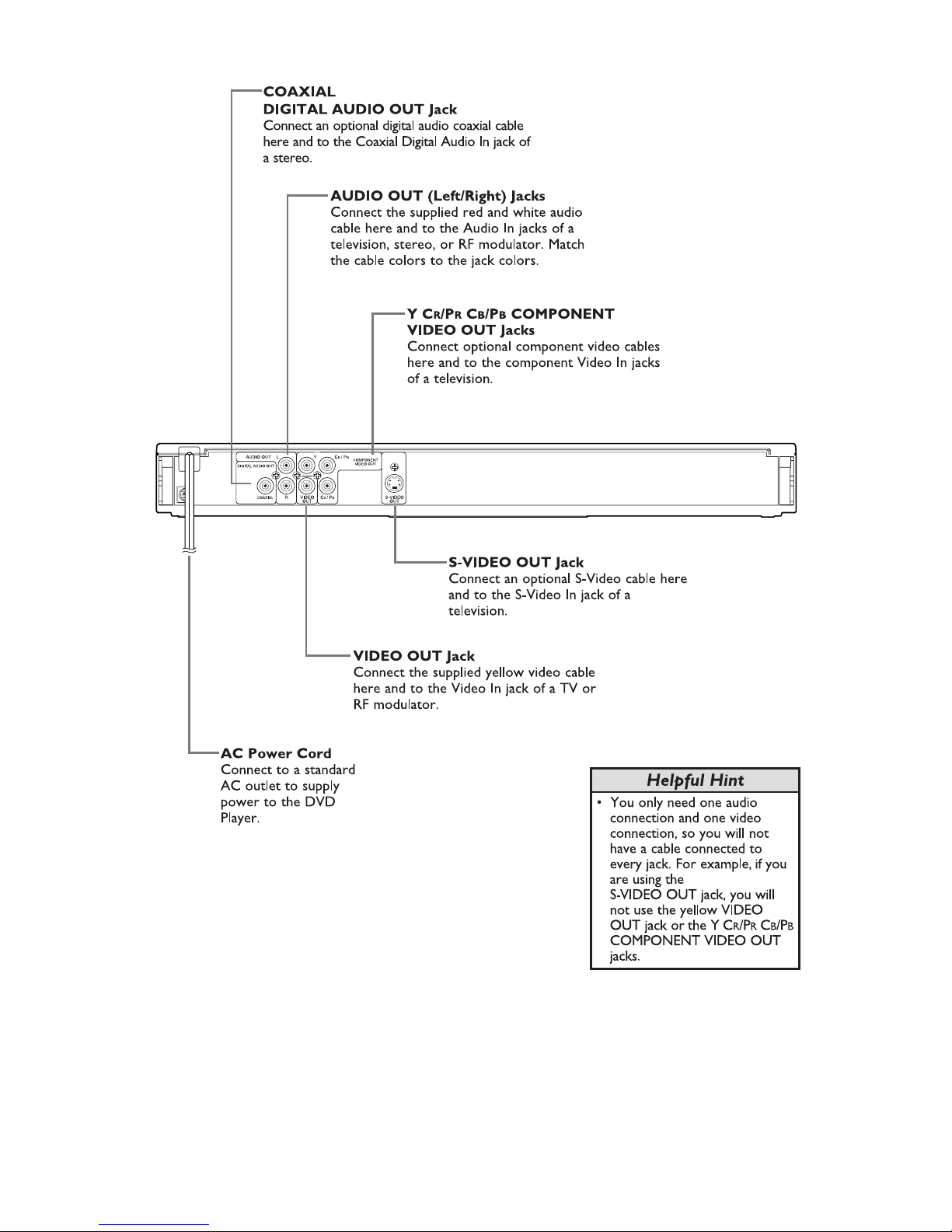
Contents
Chapter
Technical Specifications
Schematic Diagrams and CBA's
Exploded Views
Mechanical and Electrical Parts Lists
Survey of versions:
Published by FU-KC 0506 Service AV Systems Printed in The Netherlands Subject to modification
/17 NTSC
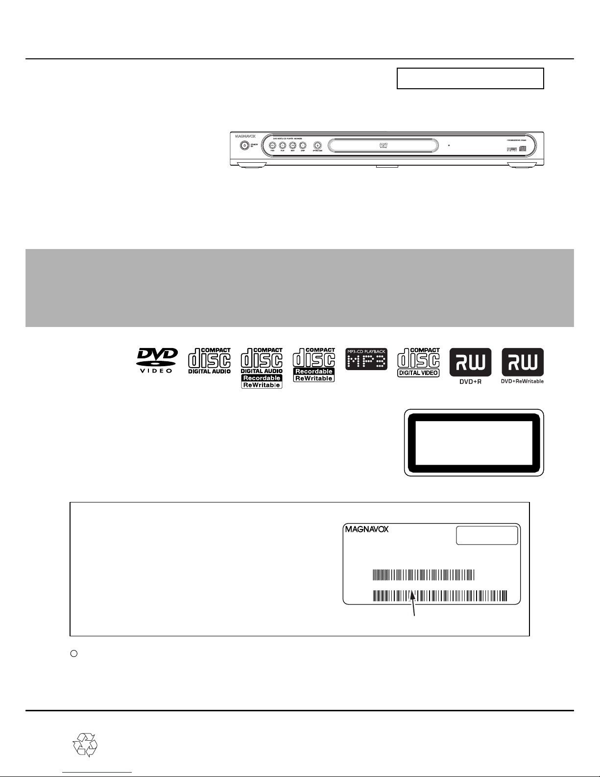
DVD Player MDV456/17
c Copyright 2005 Philips Consumer Electronics B.V. Eindhoven, The Netherlands.
All rights reserved. No part of this publication may be reproduced, stored in a retrieval
system or transmitted, in any form or by any means, electronic, mechanical, photocopying,
or otherwise without the prior permission of Philips.
CLASS 1 LASER PRODUCT
KLASSE 1 LASER PRODUKT
KLASS 1 LASER APPARAT
CLASSE 1 PRODUIT LASER
EN 3139 785 30990
Second Generation
Service Manual
Service
Service
Service
This service manual is for MDV456/17 Second
Generation model, which are different from
previous generation MDV456/17 model.
For Second Generation models, the serial
number should begin with LN2Bxxxxxxxxxx.
Refer to the rating label illustration on the right.
Rating label
SERIAL NO.
LN2Bxxxxxxxxxx
MODEL NO. MDV456/17
MODEL NO. MDV456/17
DISTRIBUTED BY
Philips Consumer Electronics North America,
Knoxville, Tennessee 37914-1810 U.S.A
DVD PLAYER
E6170UD
MANUFACTURED:D
JANUARY, 2005
Serial number
Service Information only

TABLE OF CONTENTS
LASER BEAM SAFETY PRECAUTIONS . . . . . . . . . . . . . . . . . . . . . . . . . . . . . . . . . . . . . . . . . . . . . . . . . . . . 1-1-1
IMPORTANT SAFETY PRECAUTIONS. . . . . . . . . . . . . . . . . . . . . . . . . . . . . . . . . . . . . . . . . . . . . . . . . . . . . . 1-2-1
STANDARD NOTES FOR SERVICING . . . . . . . . . . . . . . . . . . . . . . . . . . . . . . . . . . . . . . . . . . . . . . . . . . . . . . 1-3-1
OPERATING CONTROLS AND FUNCTIONS . . . . . . . . . . . . . . . . . . . . . . . . . . . . . . . . . . . . . . . . . . . . . . . . . 1-4-1
SIGNAL NAME ABBREVIATIONS. . . . . . . . . . . . . . . . . . . . . . . . . . . . . . . . . . . . . . . . . . . . . . . . . . . . . . . . . . 1-5-1
CABINET DISASSEMBLY INSTRUCTIONS . . . . . . . . . . . . . . . . . . . . . . . . . . . . . . . . . . . . . . . . . . . . . . . . . . 1-6-1
HOW TO INITIALIZE THE DVD PLAYER . . . . . . . . . . . . . . . . . . . . . . . . . . . . . . . . . . . . . . . . . . . . . . . . . . . . 1-7-1
FIRMWARE RENEWAL MODE . . . . . . . . . . . . . . . . . . . . . . . . . . . . . . . . . . . . . . . . . . . . . . . . . . . . . . . . . . . . 1-8-1
BLOCK DIAGRAMS. . . . . . . . . . . . . . . . . . . . . . . . . . . . . . . . . . . . . . . . . . . . . . . . . . . . . . . . . . . . . . . . . . . . . 1-9-1
SCHEMATIC DIAGRAMS / CBA'S AND TEST POINTS . . . . . . . . . . . . . . . . . . . . . . . . . . . . . . . . . . . . . . . . 1-10-1
WAVEFORMS . . . . . . . . . . . . . . . . . . . . . . . . . . . . . . . . . . . . . . . . . . . . . . . . . . . . . . . . . . . . . . . . . . . . . . . . 1-11-1
WIRING DIAGRAM . . . . . . . . . . . . . . . . . . . . . . . . . . . . . . . . . . . . . . . . . . . . . . . . . . . . . . . . . . . . . . . . . . . . 1-12-1
SYSTEM CONTROL TIMING CHARTS. . . . . . . . . . . . . . . . . . . . . . . . . . . . . . . . . . . . . . . . . . . . . . . . . . . . . 1-13-1
IC PIN FUNCTION DESCRIPTIONS . . . . . . . . . . . . . . . . . . . . . . . . . . . . . . . . . . . . . . . . . . . . . . . . . . . . . . . 1-14-1
LEAD IDENTIFICATIONS . . . . . . . . . . . . . . . . . . . . . . . . . . . . . . . . . . . . . . . . . . . . . . . . . . . . . . . . . . . . . . . 1-15-1
NOT IN USE....................... . . . . . . . . . . . . . . . . . . . . . . . . . . . . . . . . . . . . . . . . . . . . . . . . . . . . . . . . . . . . . . 1-16-1
EXPLODED VIEWS . . . . . . . . . . . . . . . . . . . . . . . . . . . . . . . . . . . . . . . . . . . . . . . . . . . . . . . . . . . . . . . . . . . . 1-17-1
NOT IN USE........................ . . . . . . . . . . . . . . . . . . . . . . . . . . . . . . . . . . . . . . . . . . . . . . . . . . . . . . . . . . . . . 1-18-1
Manufactured under license from Dolby Laboratories.
“Dolby” and the double-D symbol are trademarks of Dolby Laboratories.

1-1-1 E6NLSP
LASER BEAM SAFETY PRECAUTIONS
This DVD player uses a pickup that emits a laser beam.
The laser beam is emitted from the location shown in the figure. When checking the laser diode, be sure to keep
your eyes at least 30 cm away from the pickup lens when the diode is turned on. Do not look directly at the laser
beam.
CAUTION: Use of controls and adjustments, or doing procedures other than those specified herein, may result in
hazardous radiation exposure.
Location: Top of DVD mechanism.
Do not look directly at the laser beam coming
from the pickup or allow it to strike against your
skin.
Drive Mecha Assembly
Laser Beam Radiation
Laser Pickup
Turntable
LASER RADIATION
WHEN OPEN. DO NOT
STARE INTO BEAM.
CAUTION

1-2-1 DVDN_ISP
IMPORTANT SAFETY PRECAUTIONS
Product Safety Notice
Some electrical and mechanical parts have special
safety-related characteristics which are often not
evident from visual inspection, nor can the protection
they give necessarily be obtained by replacing them
with components rated for higher voltage, wattage,
etc. Parts that have special safety characteristics are
identified by a # on schematics and in parts lists. Use
of a substitute replacement that does not have the
same safety characteristics as the recommended
replacement part might create shock, fire, and/or other
hazards. The Product’s Safety is under review
continuously and new instructions are issued
whenever appropriate. Prior to shipment from the
factory, our products are carefully inspected to confirm
with the recognized product safety and electrical
codes of the countries in which they are to be sold.
However, in order to maintain such compliance, it is
equally important to implement the following
precautions when a set is being serviced.
Precautions during Servicing
A. Parts identified by the # symbol are critical for
safety. Replace only with part number specified.
B. In addition to safety, other parts and assemblies
are specified for conformance with regulations
applying to spurious radiation. These must also be
replaced only with specified replacements.
Examples: RF converters, RF cables, noise
blocking capacitors, and noise blocking filters, etc.
C. Use specified internal wiring. Note especially:
1) Wires covered with PVC tubing
2) Double insulated wires
3) High voltage leads
D. Use specified insulating materials for hazardous
live parts. Note especially:
1) Insulation tape
2) PVC tubing
3) Spacers
4) Insulators for transistors
E. When replacing AC primary side components
(transformers, power cord, etc.), wrap ends of
wires securely about the terminals before
soldering.
F. Observe that the wires do not contact heat
producing parts (heat sinks, oxide metal film
resistors, fusible resistors, etc.).
G. Check that replaced wires do not contact sharp
edges or pointed parts.
H. When a power cord has been replaced, check that
5 - 6 kg of force in any direction will not loosen it.
I. Also check areas surrounding repaired locations.
J. Be careful that foreign objects (screws, solder
droplets, etc.) do not remain inside the set.
K. Crimp type wire connector
The power transformer uses crimp type
connectors which connect the power cord and the
primary side of the transformer. When replacing
the transformer, follow these steps carefully and
precisely to prevent shock hazards.
Replacement procedure
1) Remove the old connector by cutting the wires
at a point close to the connector.
Important: Do not re-use a connector.
(Discard it.)
2) Strip about 15 mm of the insulation from the
ends of the wires. If the wires are stranded,
twist the strands to avoid frayed conductors.
3) Align the lengths of the wires to be connected.
Insert the wires fully into the connector.
4) Use a crimping tool to crimp the metal sleeve at
its center. Be sure to crimp fully to the complete
closure of the tool.
L. When connecting or disconnecting the internal
connectors, first, disconnect the AC plug from the
AC outlet.
1-2-2 DVDN_ISP
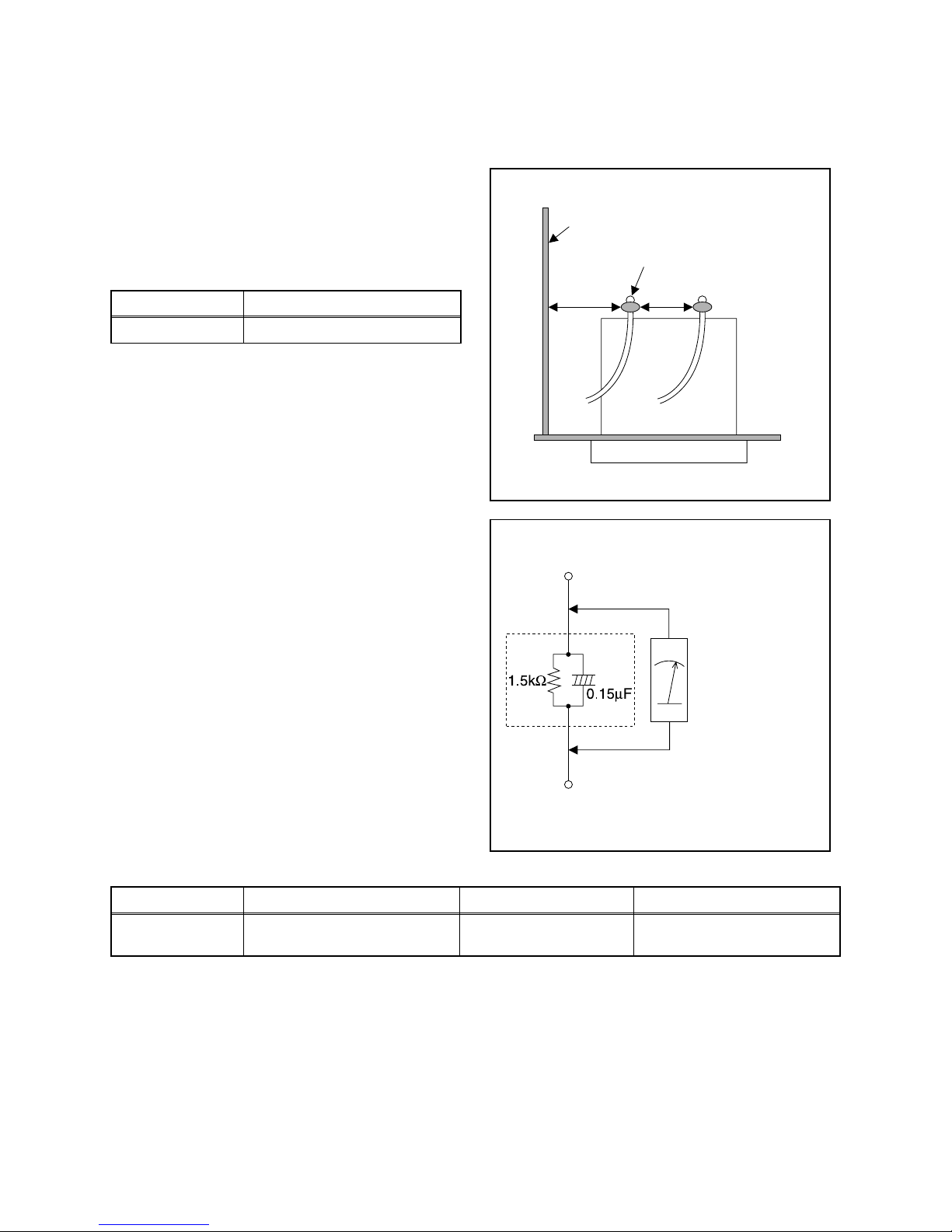
Safety Check after Servicing
Examine the area surrounding the repaired location for damage or deterioration. Observe that screws, parts, and
wires have been returned to their original positions. Afterwards, do the following tests and confirm the specified
values to verify compliance with safety standards.
1. Clearance Distance
When replacing primary circuit components, confirm
specified clearance distance (d) and (d’) between
soldered terminals, and between terminals and
surrounding metallic parts. (See Fig. 1)
Table 1: Ratings for selected area
Note: This table is unofficial and for reference only. Be
sure to confirm the precise values.
2. Leakage Current Test
Confirm the specified (or lower) leakage current
between B (earth ground, power cord plug prongs) and
externally exposed accessible parts (RF terminals,
antenna terminals, video and audio input and output
terminals, microphone jacks, earphone jacks, etc.) is
lower than or equal to the specified value in the table
below.
Measuring Method (Power ON):
Insert load Z between B (earth ground, power cord plug
prongs) and exposed accessible parts. Use an AC
voltmeter to measure across the terminals of load Z.
See Fig. 2 and the following table.
Table 2: Leakage current ratings for selected areas
Note: This table is unofficial and for reference only. Be sure to confirm the precise values.
AC Line Voltage Clearance Distance (d), (d’)
120 V ≥ 3.2 mm (0.126 inches)
AC Line Voltage Load Z Leakage Current (i) Earth Ground (B) to:
120 V
0.15 µF CAP. & 1.5 kΩ RES.
Connected in parallel
i ≤ 0.5 mA Peak Exposed accessible parts
Chassis or Secondary Conductor
dd'
Primary Circuit Terminals
Fig. 1
AC Voltmeter
(High Impedance)
Exposed Accessible Part
B
Earth Ground
Power Cord Plug Prongs
Z
Fig. 2
1-3-1 DVDN_PC_SN
STANDARD NOTES FOR SERVICING
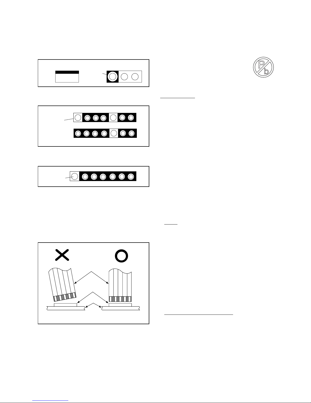
Circuit Board Indications
1. The output pin of the 3 pin Regulator ICs is
indicated as shown.
2. For other ICs, pin 1 and every fifth pin are
indicated as shown.
3. The 1st pin of every male connector is indicated as
shown.
Instructions for Connectors
1. When you connect or disconnect the FFC (Flexible
Foil Connector) cable, be sure to first disconnect
the AC cord.
2. FFC (Flexible Foil Connector) cable should be
inserted parallel into the connector, not at an
angle.
Pb (Lead) Free Solder
When soldering, be sure to use the Pb free solder.
IDENTIFICATION:
Regardless of special logo (not always
indicated)
One must treat all sets from 1.1.2005
onwards, according next rules.
Important note:
In fact also products a little older can
also be treated in this way as long as you avoid mixing
solder-alloys (leaded/ lead-free). So best to always
use SAC305 and the higher temperatures belong to
this.
Due to lead-free technology some rules have to be
respected by the workshop during a repair:
• Use only lead-free solder alloy Philips SAC305 with
order code 0622 149 00106. If lead-free solderpaste is required, please contact the manufacturer
of your solder-equipment. In general use of solderpaste within workshops should be avoided because
paste is not easy to store and to handle.
• Use only adequate solder tools applicable for lead-
free solder alloy. The solder tool must be able
• To reach at least a solder-temperature of 400°C,
• To stabilize the adjusted temperature at the solder-
tip
• To exchange solder-tips for different applications.
• Adjust your solder tool so that a temperature around
360°C
- 380°C is reached and stabilized at the
solder joint. Heating-time of the solder-joint should
not exceed ~ 4 sec. Avoid temperatures above
400°C otherwise wear-out of tips will rise drastically
and flux-fluid will be destroyed. To avoid wear-out of
tips switch off un-used equipment, or reduce heat.
• Mix of lead-free solder alloy / parts with leaded
solder alloy / parts is possible but PHILIPS
recommends strongly to avoid mixed solder alloy
types (leaded and lead-free). If one cannot avoid,
clean carefully the solder-joint from old solder alloy
and re-solder with new solder alloy (SAC305).
• Use only original spare-parts listed in the Service-
Manuals. Not listed standard-material (commodities)
has to be purchased at external companies.
• Special information for BGA-ICs:
- always use the 12nc-recognizable soldering
temperature profile of the specific BGA (for desoldering always use highest lead-free temperature
profile, in case of doubt)
- lead free BGA-ICs will be delivered in so-called
'dry-packaging' (sealed pack including a silica gel
pack) to protect the IC against moisture. After
opening, dependent of MSL-level seen on indicatorlabel in the bag, the BGA-IC possibly still has to be
baked dry. This will be communicated via AYS-
Top View
Out
In
Bottom View
Input
5
10
Pin 1
Pin 1
FFC Cable
Connector
CBA
* Be careful to avoid a short circuit.
1-3-2 DVDN_PC_SN
website.
Do not re-use BGAs at all.
• For sets produced before 1.1.2005, containing
leaded soldering-tin and components, all needed
spare-parts will be available till the end of the
service-period. For repair of such sets nothing
changes.
• On our website
www.atyourservice.ce.Philips.com
you find more
information to:
• BGA-de-/soldering (+ baking instructions)
• Heating-profiles of BGAs and other ICs used in
Philips-sets
You will find this and more technical information within
the “magazine”, chapter “workshop news”.
For additional questions please contact your local
repair-helpdesk.
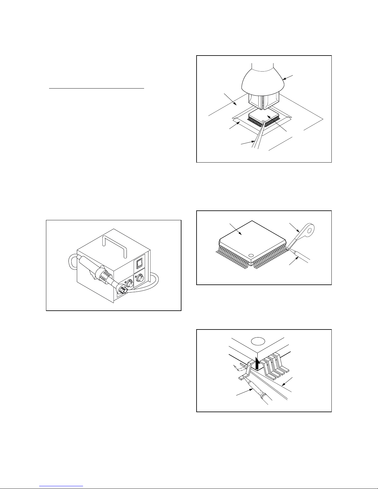
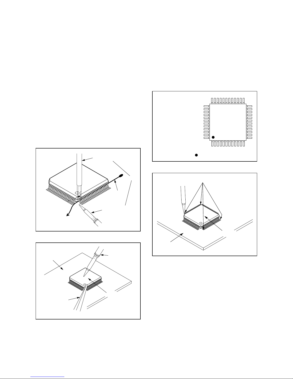
How to Remove / Install Flat Pack-IC
1. Removal
With Hot-Air Flat Pack-IC Desoldering Machine:
1. Prepare the hot-air flat pack-IC desoldering
machine, then apply hot air to the Flat Pack-IC
(about 5 to 6 seconds). (Fig. S-1-1)
2. Remove the flat pack-IC with tweezers while
applying the hot air.
3. Bottom of the flat pack-IC is fixed with glue to the
CBA; when removing entire flat pack-IC, first apply
soldering iron to center of the flat pack-IC and heat
up. Then remove (glue will be melted). (Fig. S-1-6)
4. Release the flat pack-IC from the CBA using
tweezers. (Fig. S-1-6)
CAUTION:
1. The Flat Pack-IC shape may differ by models. Use
an appropriate hot-air flat pack-IC desoldering
machine, whose shape matches that of the Flat
Pack-IC.
2. Do not supply hot air to the chip parts around the
flat pack-IC for over 6 seconds because damage
to the chip parts may occur. Put masking tape
around the flat pack-IC to protect other parts from
damage. (Fig. S-1-2)
3. The flat pack-IC on the CBA is affixed with glue, so
be careful not to break or damage the foil of each
pin or the solder lands under the IC when
removing it.
With Soldering Iron:
1. Using desoldering braid, remove the solder from
all pins of the flat pack-IC. When you use solder
flux which is applied to all pins of the flat pack-IC,
you can remove it easily. (Fig. S-1-3)
2. Lift each lead of the flat pack-IC upward one by
one, using a sharp pin or wire to which solder will
not adhere (iron wire). When heating the pins, use
a fine tip soldering iron or a hot air desoldering
machine. (Fig. S-1-4)
3. Bottom of the flat pack-IC is fixed with glue to the
CBA; when removing entire flat pack-IC, first apply
soldering iron to center of the flat pack-IC and heat
up. Then remove (glue will be melted). (Fig. S-1-6)
4. Release the flat pack-IC from the CBA using
tweezers. (Fig. S-1-6)
Fig. S-1-1
Hot-air
Flat Pack-IC
Desoldering
Machine
CBA
Flat Pack-IC
Tweezers
Masking
Tape
Fig. S-1-2
Flat Pack-IC
Desoldering Braid
Soldering Iron
Fig. S-1-3
Fine Tip
Soldering Iron
Sharp
Pin
Fig. S-1-4
1-3-3 DVDN_PC_SN
With Iron Wire:
1. Using desoldering braid, remove the solder from
all pins of the flat pack-IC. When you use solder
flux which is applied to all pins of the flat pack-IC,
you can remove it easily. (Fig. S-1-3)
2. Affix the wire to a workbench or solid mounting
point, as shown in Fig. S-1-5.
3. While heating the pins using a fine tip soldering
iron or hot air blower, pull up the wire as the solder
melts so as to lift the IC leads from the CBA
contact pads as shown in Fig. S-1-5.
4. Bottom of the flat pack-IC is fixed with glue to the
CBA; when removing entire flat pack-IC, first apply
soldering iron to center of the flat pack-IC and heat
up. Then remove (glue will be melted). (Fig. S-1-6)
5. Release the flat pack-IC from the CBA using
tweezers. (Fig. S-1-6)
Note: When using a soldering iron, care must be
taken to ensure that the flat pack-IC is not
being held by glue. When the flat pack-IC is
removed from the CBA, handle it gently
because it may be damaged if force is applied.
2. Installation
1. Using desoldering braid, remove the solder from
the foil of each pin of the flat pack-IC on the CBA
so you can install a replacement flat pack-IC more
easily.
2. The “●” mark on the flat pack-IC indicates pin 1.
(See Fig. S-1-7.) Be sure this mark matches the 1
on the PCB when positioning for installation. Then
presolder the four corners of the flat pack-IC. (See
Fig. S-1-8.)
3. Solder all pins of the flat pack-IC. Be sure that
none of the pins have solder bridges.
To Solid
Mounting Point
Soldering Iron
Iron Wire
or
Hot Air Blower
Fig. S-1-5
Fine Tip
Soldering Iron
CBA
Flat Pack-IC
Tweezers
Fig. S-1-6
Example :
Pin 1 of the Flat Pack-IC
is indicated by a " " mark.
Fig. S-1-7
Presolder
CBA
Flat Pack-IC
Fig. S-1-8
1-3-4 DVDN_PC_SN
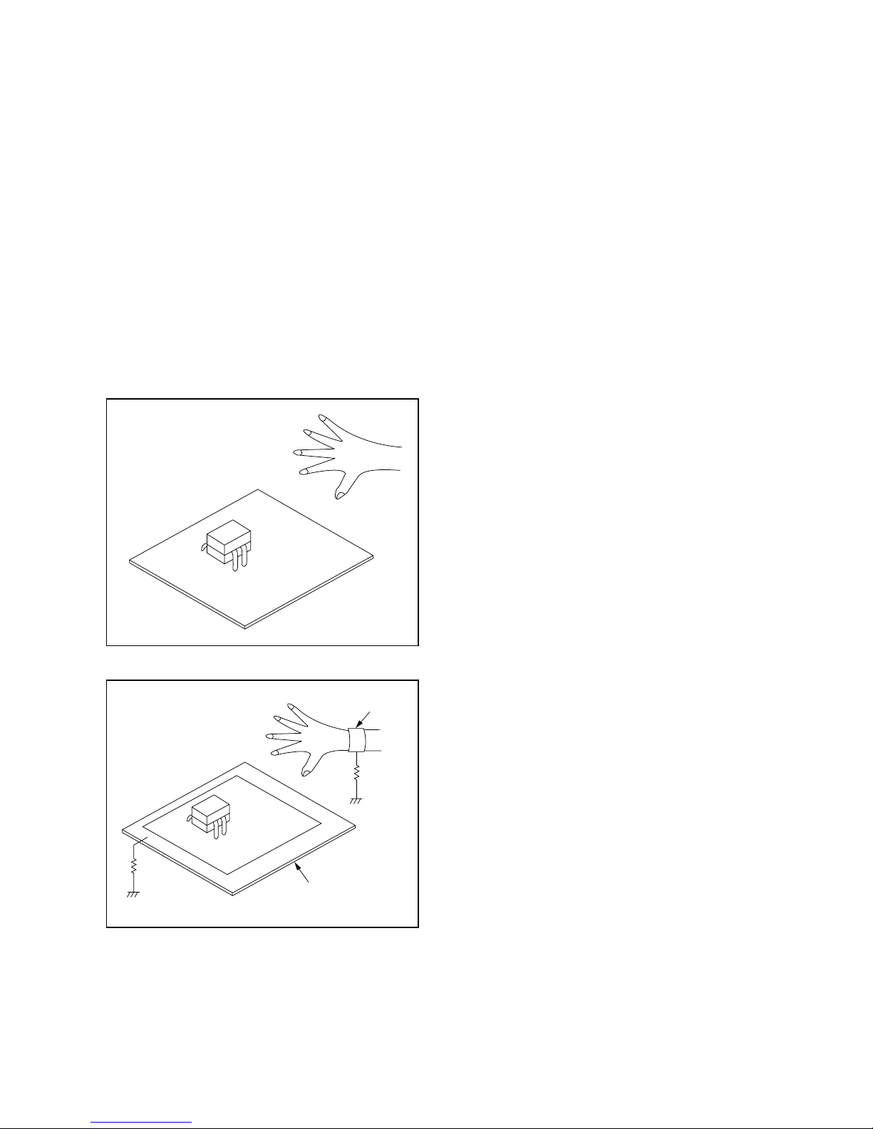
Instructions for Handling Semiconductors
Electrostatic breakdown of the semi-conductors may
occur due to a potential difference caused by
electrostatic charge during unpacking or repair work.
1. Ground for Human Body
Be sure to wear a grounding band (1 MΩ) that is
properly grounded to remove any static electricity that
may be charged on the body.
2. Ground for Workbench
Be sure to place a conductive sheet or copper plate
with proper grounding (1 MΩ) on the workbench or
other surface, where the semi-conductors are to be
placed. Because the static electricity charge on
clothing will not escape through the body grounding
band, be careful to avoid contacting semi-conductors
with your clothing.
<Incorrect>
CBA
Grounding Band
Conductive Sheet or
Copper Plate
1MΩ
1MΩ
<Correct>
CBA
1-4-1 E6170IB
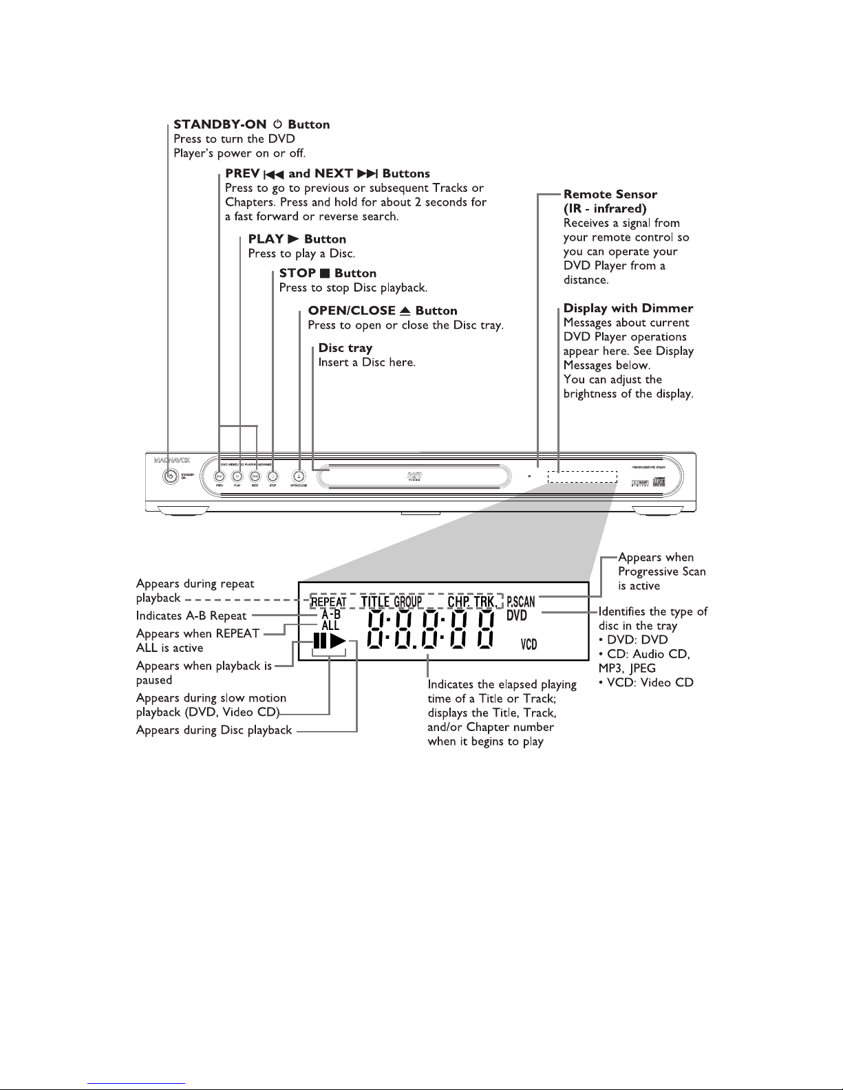
OPERATING CONTROLS AND FUNCTIONS
1-4-2 E6170IB
1-4-3 E6170IB
1-4-4 E6170IB
1-5-1 E6170SNA
SIGNAL NAME ABBREVIATIONS
Signal Name Function
-FL FIP Drive Power Supply
AUDIO(L) Audio (L) Signal
AUDIO(R) Audio (R) Signal
AUDIO(R)MUTE
Audio (R) Mute Control Signal
AUDIO+5V +5V at Audio Signal
AUDIO-GND Audio Ground Signal
EV+1.2V +1.2V Power Supply
EV+10V +10V Power Supply
EV+3.3V +3.3V Power Supply
EV+5V +5V Power Supply
F1 Filament Power Supply 1
F2 Filament Power Supply 2
FP-CLK Clock Input
FP-DIN Serial Data Input
FP-DOUT Serial Data Output
FP-STB Serial Interface Strobe
I/P-SW
Interlace/Progressive Detector
Signal
K1 Key Data 1 Input
K2 Key Data 2 Input
KEY-1 Key Souce-1
KEY-2 Key Souce-2
KEY-3 Key Souce-3
KEY-4 Key Souce-4
OSC Oscillator Input
P-ON+3.3V +3.3V at Power-On Signal
P-ON+5V +5V at Power-On Signal
P-ON+9V +9V at Power-On Signal
PWRCON Power Down
REMOTE Remote Control Signal
SPDIF
Digital Audio Interface Format
Signal
VDD Power Supply
VEE Pull Down Level
VIDEO-C
C (chrominance) Component Video
Signal
VIDEO-Cb/Pb Cb/Pb Component Video Signal
VIDEO-Cr/Pr Cr/Pr Component Video Signal
VIDEO-Y(I/P)
Y (luminance) Component Video
Signal (Interlace/Progressive)
VSS GND

1-6-1 E6170DC
CABINET DISASSEMBLY INSTRUCTIONS
1. Disassembly Flowchart
This flowchart indicates the disassembly steps to gain
access to item(s) to be serviced. When reassembling,
follow the steps in reverse order. Bend, route, and
dress the cables as they were originally.
2. Disassembly Method
Note:
(1) Identification (location) No. of parts in the figures
(2) Name of the part
(3) Figure Number for reference
(4) Identification of parts to be removed, unhooked,
unlocked, released, unplugged, unclamped, or
desoldered.
P = Spring, L = Locking Tab, S = Screw,
CN = Connector
* = Unhook, Unlock, Release, Unplug, or Desolder
e.g. 2(S-2) = two Screws (S-2),
2(L-2) = two Locking Tabs (L-2)
(5) Refer to “Reference Notes.”
About tightening screws
When tightening screws, tighten them with the
following torque.
Reference Notes
1. CAUTION 1: Locking Tabs (L-1), (L-2) and (L-3)
are fragile. Be careful not to break them.
1) Release four Locking Tabs (L-1). Then, release
three Locking Tabs (L-2).
2) Release three Locking Tabs (L-3). Then
remove the Front Assembly.
2. CAUTION 2: Electrostatic breakdown of the laser
diode in the optical system block may occur as a
potential difference caused by electrostatic charge
accumulated on cloth, human body etc, during
unpacking or repair work.
To avoid damage of pickup follow next procedures.
1) Short the three short lands of FPC cable with
solder before removing the FFC cable (CN201)
from it. If you disconnect the FFC cable
(CN201), the laser diode of pickup will be
destroyed. (Fig. D4)
2) Disconnect Connectors (CN301), (CN401) and
(CN601). Remove two Screws (S-3A) and (S3B) and lift the DVD Main CBA Unit. (Fig. D4)
3. CAUTION 3: When reassembling, confirm the
FFC cable (CN201) is connected completely. Then
remove the solder from the three short lands of
FPC cable. (Fig. D4)
ID/
Loc.
No.
Part
Removal
Fig.
No.
Remove/*Unhook/
Unlock/Release/
Unplug/Desolder
Note
[1] Top Case D1 3(S-1) -
[2]
Front
Assembly
D2
*4(L-1), *3(L-2),
*3(L-3)
1
[3]
Reinforce
Plate
D3 2(S-2) -
[4]
DVD M a i n
CBA Unit
D4
(S-3A), (S-3B),
*CN201, *CN301,
*CN401, *CN601
2
[5] DVD Mecha
D4
D5
4(S-4)
2
3
[6] AV CBA D6 (S-5), 4(S-6), *2(L-4) -
[7]
Function
CBA
D6 *CN2001 -
↓
(1)
↓
(2)
↓
(3)
↓
(4)
↓
(5)
[1] Top Case
[2] Front Assembly
[3] Reinforce Plate
[4] DVD Main CBA Unit
[5] DVD Mecha [6] AV CBA
[7] Function CBA
Screws Torque
(S-1), (S-2), (S-3A), (S-4),
(S-5), (S-6)
0.45 ± 0.05 N·m
(S-3B) 0.38 ± 0.04 N·m
(S-1)
[1] Top Case
Fig. D1

1-6-2 E6170DC
[2] Front Assembly
(L-2)
(L-3)
(L-1)
(L-1)
Fig. D2
Fig. D3
(S-2)
(S-2)
[3] Reinforce Plate
[4] DVD Main
CBA Unit
CN201
CN301
CN401
CN601
A
(S-3B)
(S-3A)
Fig. D4
View for A
Short the three short lands by soldering.
(Either of two places.)
Connector
[5] DVD Mecha
(S-4)
(S-4)
(S-4)
Fig. D5

1-6-3 E6170DC
3. How to Eject Manually
1. Turn the unit over.
2. Insert the shaft less than a diameter of 3 mm (e.g. screwdriver) straightly into the opening as shown.
3. Turn the shaft along with the opening clockwise.
4. Repeat steps 2 and 3 until the tray will open.
5. Pull the tray slowly with a hand.
[7] Function CBA
[6] AV CBA
(S-5)
(S-6)
CN2001
(L-4)
Fig. D6
B
Front
View for B
Turn the shaft along with
the opening clockwise.
Rear
Opening
Shaft
(e.g. screwdriver)

1-7-1 E6170INT
HOW TO INITIALIZE THE DVD PLAYER
To put the program back at the factory-default,
initialize the DVD player as the following procedure.
1. Press [1], [2], [3], [4], and [DISPLAY] buttons on
the remote control unit in that order.
Fig. a appears on the screen.
2. Press [CLEAR] button on the remote control unit.
Fig. b appears on the screen.
When “OK” appears on the screen, the factory
default will be set. Then the firmware renewal
mode is complete.
3. To exit this mode, press [STANDBY-ON y] button.
MODEL : *******
Version
: *.**
Region
: *
EXIT: POWEREEPROM CLEAR : CLEAR
Fig. a
"
*******
" differ depending on the models.
MODEL : *******
Version
: *.**
Region
: *
EEPROM CLEAR : OK
EXIT: POWEREEPROM CLEAR : CLEAR
"
*******
" differ depending on the models.
Fig. b

1-8-1 E6170FW
FIRMWARE RENEWAL MODE
1. Turn the power on and remove the disc on the tray.
2. To put the DVD player into version up mode, press
[9], [8], [7], [6], and [SEARCH MODE] buttons on
the remote control unit in that order. The tray will
open automatically.
Fig. a appears on the screen and Fig. b appears
on the VFD.
The DVD player can also enter the version up
mode with the tray open. In this case, Fig. a will be
shown on the screen while the tray is open.
3. Load the disc for version up.
4. The DVD player enters the F/W version up mode
automatically. Fig. c appears on the screen and
Fig. d appears on the VFD. If you enter the F/W for
different models, “Disc Error” will appear on the
screen, then the tray will open automatically.
The appearance shown in (*1) of Fig. c is
described as follows:
5. After programming is finished, the tray opens
automatically. Fig. e appears on the screen and
the checksum in (*2) of Fig. e appears on the VFD.
(Fig. f)
At this time, no buttons are available.
6. Remove the disc on the tray.
7. Unplug the AC cord from the AC outlet. Then plug
it again.
8. Turn the power on by pressing the
[STANDBY-ON y] button and the tray will close.
9. Press [1], [2], [3], [4], and [DISPLAY] buttons on
the remote control unit in that order.
Fig. g appears on the screen.
10. Press [CLEAR] button on the remote control unit.
Fig. h appears on the screen.
When “OK” appears on the screen, the factory
default will be set. Then the firmware renewal
mode is complete.
11. To exit this mode, press [STANDBY-ON y] button.
No. Appearance State
1 Reading... Sending files into the memory
2 Erasing... Erasing previous version data
3 Programming... Writing new version data
F/W Version Up Mode Model No : *******
VERSION : *.**
Please insert a DISC
for F/W Version Up.
EXIT: POWER
"
*******
" differ depending on the models.
Fig. a Version Up Mode Screen
Fig. b VFD in Version Up Mode
VERSION : ************.ab6
Reading...
F/W Version Up Mode Model No : *******
VERSION : *.**
Fig. c Programming Mode Screen
"
*******
" differ depending on the models.
(*1)
Fig. d VFD in Programming Mode (Example)
VERSION : ************.ab6
Completed
SUM : 7ABC
F/W Version Up Mode
Model No : *******
VERSION : *.**
"
*******
" differ depending on the models.
Fig. e Completed Program Mode Screen
(*2)
Fig. f VFD upon Finishing the Programming Mode (Example)
MODEL : *******
Version
: *.**
Region
: *
EXIT: POWEREEPROM CLEAR : CLEAR
Fig. g
"
*******
" differ depending on the models.
MODEL : *******
Version
: *.**
Region
: *
EEPROM CLEAR : OK
EXIT: POWEREEPROM CLEAR : CLEAR
"
*******
" differ depending on the models.
Fig. h

1-9-1
E6170BLS
BLOCK DIAGRAMS
System Control / Servo Block Diagram
82
FP-STB
60
FP-DIN
61
FP-DOUT
67
REMOTE
59
FP-CLK
CN401
IC301
(SERVO DRIVE)
2120221923
CN301
M
SLED
MOTOR
M
SPINDLE
MOTOR
IC101
(MICRO CONTROLLER)
+
-
+
-
+
-
+
-
+
-
+
-
+
-
SLED
MOTOR
DRIVE
FOCUS
ACTUATOR
DRIVE
SPINDLE
MOTOR
DRIVE
TRACKING
ACTUATOR
DRIVE
147
TRAY-IN
SLD
75
SPDL
76
TRACKING
DRIVE
148
FOCUS DRIVE
66
FS(+)
FS(-)
TS(+)
TS(-)
57
ADAC-MD
56 ADAC-MC
86 ADAC-ML
ADAC-MC
ADAC-ML
PCM-SCLK
88
ADAC-MD
163
PCM-SCLK
TRAY-IN
3SP(+)
4SP(-)
5TRAY-IN
6GND
7SL(-)
8SL(+)
VREF
CN1001
2
28
27
1
12
789
10
11
REMOTE
SENSOR
RM2001
1G
7G
~
23
17
~
a/KEY-1
b/KEY-2
c/KEY-3
d/KEY-4
e
K1
K2
FP-STB
FP-DIN
FP-DOUT
FP-CLK
GRID FIP
SEGMENT
FL2001
IC2001
(FRONT PANEL CONTROL)
131416
3
4
f
g
h
i
KEY
MATRIX
CN2001 CN2101
FP-STB 23
FP-DIN 22
FP-DOUT 24
FP-CLK 21
REMOTE 25
RESET73
RESET
IC462
1 3
+3.3V
IC202
(OP AMP)
15
16
14
13
12
11
17
18
23
645
312
25
24
27
26
81
SL-AMP
143
SP-ROT
+3.3V
146
FD-OFST
139
TD-OFST
RESET
IC461
2 1
+3.3V
TO DIGITAL SIGNAL
PROCESS BLOCK
DIAGRAM
TO
VIDEO/ AUDIO
BLOCK DIAGRAM
DRIVE CBA
DVD MAIN CBA UNIT AV CBA
FUNCTION CBA
1
2
6
7
5
3
13
14
12
KEY-1 5
KEY-2 3
KEY-3 4
KEY-4 6
K2 1
K1 2
53461
2
183
I/P-SW
I/P-SW
AUDIO-MUTE
AUDIO-MUTE
*1
140
SL-ADS
“ “ = SMD
NOTE FOR WIRE CONNECTORS:
1. PREFIX SYMBOL "CN" MEANS CONNECTOR.
(CAN DISCONNECT AND RECONNECT.)
2. PREFIX SYMBOL "CL" MEANS WIRE-SOLDER
HOLES OF THE PCB.
(WIRE IS SOLDERED DIRECTLY.)
1 NOTE:
Either IC461 or IC462 is used for DVD MAIN CBA UNIT.

1-9-2
E6170BLD
Digital Signal Process Block Diagram
C16
D18
A17
B15
E14
F12
DVD-LD 8
CD-LD 10
PD-MONI 7
CN201
CN201
CN201
IC201
(SW)
IC503 (SDRAM) IC101 (MICRO CONTROLLER)
FS
FS(+)
CD/DVD
FS(-)
TS(+)
TS(-)
TS
DETECTOR
CD/DVD 19
Q251,Q252
CD DVD
AMP
Q253,Q254
AMP
4
1 3
6
GND(DVD-PD)
6
GND(CD-PD)
5
GND(LD)
9
RF
SIGNAL
PROCESS
CIRCUIT
DVD/CD
FORMATTER
AUDIO
I/F
VIDEO
I/F
NTSC/PAL
ENCODER
DMA
BCU
INST.
ROM
32BIT
CPU
DATA
RAM
INTERRUPT
CONTROLLER
WATCH DOG
TIMER
CPU
I/F
TIMER
DECODER
I/F
CPU
I/F
READ
MEMORY
DATA
RAM
DSP
DECODER
I/O
PROCESSOR
INST.
ROM
DATA
RAM
INST.
ROM
SERIAL
D/A
GENERAL
I/O
INTERRUPT
CONTROLLER
TIMER
WATCH DOG
TIMER
REMOTE
CONTROL
32BIT CPU
STREAM
I/F
EXTERNAL
MEMORY
I/F
SDRAM
ECC
UMAC
114
115
116
117
132
131
134
133
129
130
126
124
125
123
83
DEBUG
BCU
INST.
CACHE
DATA
CACHE
D/A
D/A
D/A
149
158
Y(I/P)
C
Cr/Pr
Cb/Pb
VIDEO-Y(I/P)
VIDEO-C
VIDEO-Cr/Pr
VIDEO-Cb/Pb
177
SPDIF
170
PCM-BCK
171
PCM-DATA
169
PCM-LRCLK
152
151
23~51
SDRAM DATA(0-15)
SDRAM ADDRESS(0-11)
SDRAM ADDRESS(0-11)
217
238
~
1
18
252
256
~~
2
134253
~~
IC103 (FLASH ROM)
FLASH
ROM
293638
45
~
~
DATA(VIDEO/AUDIO) SIGNAL VIDEO SIGNAL
DATA(AUDIO) SIGNAL
222629
35
~~
EXT MEMORY DATA (0-15)
~
1
9
162548
~
192~212
EXT ADR (0-19)
SDRAM DATA(0-15)
PICK-UP
UNIT
TO SYSTEM
CONTROL/SERVO
BLOCK DIAGRAM
DVD MAIN CBA UNIT
TO
VIDEO
/AUDIO
BLOCK
DIAGRAM
TO
VIDEO
/AUDIO
BLOCK
DIAGRAM
FS(+) 2
FS(-) 3
TS(+) 1
TS(-) 4
“ “ = SMD
NOTE FOR WIRE CONNECTORS:
1. PREFIX SYMBOL "CN" MEANS CONNECTOR.
(CAN DISCONNECT AND RECONNECT.)
2. PREFIX SYMBOL "CL" MEANS WIRE-SOLDER
HOLES OF THE PCB.
(WIRE IS SOLDERED DIRECTLY.)

1-9-3
E6170BLV
Video / Audio Block Diagram
IC601 (AUDIO DAC)
15
14
16
JK1404
IC1201
Q1201
Q1202
+5V
(AMP)
CN601 CN1601
13 13AUDIO(L)
15
15
AUDIO(R)
14 14
AUDIO(R)-MUTE
AUDIO(L)-
OUT
768
432
5
AUDIO
SERIAL
PORT
SERIAL
CONTROL
PORT
4X/8X
OVERSAMPLING
DIGITAL FILTER
/FUNCTION
CONTROLLER
ENHANCED
MULTI-LEVEL
DELTA-SIGMA
MODULATOR
DAC
LPF+AMP
L-CH
R-CH
LPF+AMP
DAC
ZERO DETECT
SYSTEM CLOCK
MANAGER
1
2
7
5
AUDIO(R)-
OUT
PCM-BCK
SPDIF
PCM-DATA
PCM-LRCLK
ADAC-MD
ADAC-MC
ADAC-ML
PCM-SCLK
18
18
SPDIF
AUDIO-MUTE
+3.3V
Q1204
3
88VIDEO-Y(I/P)
10 10VIDEO-C
66VIDEO-Cb/Pb
44VIDEO-Cr/Pr
VIDEO-Y(I/P)
VIDEO-C
VIDEO-Cb/Pb
VIDEO-Cr/Pr
JK1401
S-VIDEO OUT
3 4
2
1
YC
CN601 CN1601
AUDIO SIGNALDATA(AUDIO) SIGNAL
VIDEO SIGNAL
TO
SYSTEM
CONTROL
/SERVO
BLOCK
DIAGRAM
TO
DIGITAL
SIGNAL
PROCESS
BLOCK
DIAGRAM
TO DIGITAL
SIGNAL PROCESS
BLOCK DIAGRAM
DVD MAIN CBA UNIT AV CBA
VIDEO OUT
(COMPOSITE)
VIDEO-Cb/Pb
OUT
VIDEO-Y
OUT
VIDEO-Cr/Pr
OUT
JK1404
6
AMP
Q1351
JK1202
IC1402 (VIDEO DRIVER)
18
4dB
AMP
2dB
AMP
LPF DRIVER
21
2dB
AMP
DRIVER
4dB
AMP
2dB
AMP
LPF DRIVER
15
4dB
AMP
2dB
AMP
LPF DRIVER
9
13
4dB
AMP
2dB
AMP
LPF DRIVER
11
6
2
23
MUTE
3
2
2
I/P-SW
I/P-SW
DIGITAL
AUDIO OUT
(COAXIAL)
WF1 WF2
WF3
WF6
WF4 WF5
“ “ = SMD
NOTE FOR WIRE CONNECTORS:
1. PREFIX SYMBOL "CN" MEANS CONNECTOR.
(CAN DISCONNECT AND RECONNECT.)
2. PREFIX SYMBOL "CL" MEANS WIRE-SOLDER
HOLES OF THE PCB.
(WIRE IS SOLDERED DIRECTLY.)

1-9-4
E6170BLP
Power Supply Block Diagram
IC1006
(SHUNT REGULATOR)
AC1001
AC CORD
F1001
LINE
FILTER
L1001
D1001, D1002
D1004, D1005
Q1003
2
4
7
3
4
IC1001
ERROR
VOLTAGE DET
T1001
11
12
131514
16
17
18
SWITCHING
SWITCHING
CONTROL
1
2
6
BRIDGE
RECTIFIER
HOT
HOT CIRCUIT. BE CAREFUL.
D1003
RECTIFIER
D1030
RECTIFIER
D1016
RECTIFIER
Q1016
Q1005
Q1011
Q1015
Q1002
CN1001
Q1004
-FL
EV+5V
F1
P-ON+9V
EV+3.3V
P-ON+5V
4,5
EV+1.2V
6,7,8
EV+3.3V
11,12
EV+10V10P-ON+5V9P-ON+3.3V20PWRCON
D1006
SCHOTTKY
BARRIER
SCHOTTKY
BARRIER
D1008
F2
AV CBA
TO CN401
Q1031
1A 250V
3
+1.2V
REG.
IC1002
3
1
2
A V
F
REG
312
NOTE FOR WIRE CONNECTORS:
1. PREFIX SYMBOL "CN" MEANS CONNECTOR.
(CAN DISCONNECT AND RECONNECT.)
2. PREFIX SYMBOL "CL" MEANS WIRE-SOLDER
HOLES OF THE PCB.
(WIRE IS SOLDERED DIRECTLY.)
CAUTION !
Fixed voltage ( or Auto voltage selectable ) power supply circuit is used in this unit.
If Main Fuse(F1001)is blown , check to see that all components in the power supply
circuit are not defective before you connect the AC plug to the AC power supply.
Otherwise it may cause some components in the power supply circuit to fail.
NOTE:
The voltage for parts in hot circuit is measured using
hot GND as a common terminal.
"Ce symbole reprèsente un fusible à fusion rapide."
CAUTION !
For continued protection against fire hazard,
replace only with the same type fuse.
ATTENTION : Pour une protection continue les risqes
d'Incele n'utiliser que des fusible de même type.
Risk of fire-replace fuse as marked.
"This symbol means fast operating fuse."
A V
F

1-10-1 E6N_PC_SC
SCHEMATIC DIAGRAMS / CBA’S AND TEST POINTS
Standard Notes
WARNING
Many electrical and mechanical parts in this chassis
have special characteristics. These characteristics
often pass unnoticed and the protection afforded by
them cannot necessarily be obtained by using
replacement components rated for higher voltage,
wattage, etc. Replacement parts that have these
special safety characteristics are identified in this
manual and its supplements; electrical components
having such features are identified by the mark “#” in
the schematic diagram and the parts list. Before
replacing any of these components, read the parts list
in this manual carefully. The use of substitute
replacement parts that do not have the same safety
characteristics as specified in the parts list may create
shock, fire, or other hazards.
Capacitor Temperature Markings
Capacitors and transistors are represented by the
following symbols.
Notes:
1. Do not use the part number shown on these
drawings for ordering. The correct part number is
shown in the parts list, and may be slightly
different or amended since these drawings were
prepared.
2. To maintain original function and reliability of
repaired units, use only original replacement parts
which are listed with their part numbers in the
parts list section of the service manual.
3. How to read converged lines.
Examples:
1) “1-D3” means that line number “1” goes to area
“D3”.
2) “1-B1” means that line number “1” goes to area
“B1”.
4. All resistance values are indicated in ohms
(K = 10
3
, M = 106).
5. Resistor wattages are 1/6W unless otherwise
specified.
6. All capacitance values are indicated in µF
(P = 10
-6
µF).
7. All voltages are DC voltages unless otherwise
specified.
8. Voltage indications for PLAY and STOP modes on
the schematics are as shown below.
Mark
Capacity
change rate
Standard
temperature
Temperature
range
(B)
±10% 20°C -25~+85°C
(F)
±30 - 80% 20°C –25~+85°C
(SR)
±15% 20°C –25~+85°C
(Y)
±22.5% 20°C –25~+85°C
3
2
1
ABCD
1-B1
1-D3
AREA D3
AREA B1
1-D3
Distinction Area
Line Number
(1 to 3 digits)
2
3
1
5.0
(2.5)
5.0
The same voltage for
both PLAY & STOP modes
Indicates that the voltage
is not consistent here.
PLAY mode
STOP mode
(Unit: Volt)
(Top View) (Bottom View)
(Bottom View)
Electrolytic Capacitor
+
Transistor or Digital Transistor
NPN Transistor
PNP Transistor
NPN Digital Transistor
PNP Digital
Transistor
(Top View)
(Top View)
E C B
E C B
Digital Transistor
< PCB Symbols >
< Schematic Diagram Symbols >
E C B
(Top View)
(Top View)
E C B
E C B

AV 1/3 Schematic Diagram Parts Location Guide
1-10-2
Ref No. Position Ref No. Position Ref No. Position
C1001 A-4 D1024 B-1 R1019 C-1
C1003 B-4 D1030 C-3 R1020 C-1
C1004 A-3 D1046 D-2 R1021 C-1
C1005 B-3 D1047 E-2 R1022 C-1
C1006 A-3 D1048 C-3 R1023 C-1
C1007 C-3 D1053 D-3 R1025 D-3
C1009 D-2 D1054 D-1 R1029 A-2
C1010 B-3 D1055 D-2 R1032 B-1
C1013 B-2 D1058 E-1 R1035 B-1
C1014 C-3 D1059 E-4 R1043 B-4
C1017 B-2 D1073 B-2 R1044 D-3
C1018 C-2 D2045 D-3 R1059 E-1
C1021 C-2 R1061 C-4
C1022 C-1 IC1001 B-1 R1062 C-4
C1029 B-2 IC1002 D-4 R1067 D-1
C1034 E-4 IC1006 C-1 R1068 D-2
C1035 C-3 R1069 E-3
C1036 C-1 L1001 A-4 R1072
E-4
C1037 D-2 L1007 C-3 R1073
D-3
C1038 C-3 L1009 C-3 R1074 C-4
C1039
D-4
R1075 D-3
C1047
C-3
Q1002
D-2
R1076 D-4
C1048
C-3
Q1003
B-2
R1078 D-4
C1049
C-4
Q1004
D-3
R1079 C-2
Q1005
D-2
R1080 E-1
CN1001 F-4 Q1011
D-1
R1081 C-1
Q1015
D-2
R1083 E-2
D1001 A-4 Q1016
E-2
R1084 D-2
D1002 A-4 Q1031
B-3
R1085 D-2
D1003 C-4 R1086 E-1
D1004 A-4 R1002 C-4 R1091 E-2
D1005 A-4 R1004 B-4 R1095 E-4
D1006 C-3 R1005 B-3
D1008
C-3 R1006 B-3 AC1001 A-4
D1011 B-3
R1008 B-3 F1001 A-4
D1012 B-2
R1010 B-2 SA100 A-3
D1016 C-3 R1011 B-3 T1001 B-4
D1017 C-2
R1015 B-2
D1018 B-1 R1016 B-2
TRANSISTORS
DIODES
RESISTORS
MISCELLANEOUS
CONNECTOR
DIODES RESISTORS
ICS
CAPACITORS
COILS

E6170SCAV1
AV 1/3 Schematic Diagram
CAUTION !
Fixed voltage ( or Auto voltage selectable ) power supply circuit is used in this unit.
If Main Fuse(F1001)is blown , check to see that all components in the power supply
circuit are not defective before you connect the AC plug to the AC power supply.
Otherwise it may cause some components in the power supply circuit to fail.
NOTE:
The voltage for parts in hot circuit is measured using
hot GND as a common terminal.
"Ce symbole reprèsente un fusible à fusion rapide."
CAUTION !
For continued protection against fire hazard,
replace only with the same type fuse.
ATTENTION : Pour une protection continue les risqes
d'Incele n'utiliser que des fusible de même type.
Risk of fire-replace fuse as marked.
"This symbol means fast operating fuse."
A V
F
Voltage indications for PLAY and STOP modes
on the Schematic Diagrams are as shown below:
1
2
3
5.0
(2.5)
~
5.0
The same voltage for
both PLAY & STOP modes.
Indicates that the voltage
is not consistent here.
PLAY mode
STOP mode
“ “ = SMD
1-10-3

E6170SCAV2
AV 2/3 Schematic Diagram
Voltage indications for PLAY and STOP modes
on the Schematic Diagrams are as shown below:
1 2 3
5.0
(2.5)
~
5.0
The same voltage for
both PLAY & STOP modes.
Indicates that the voltage
is not consistent here.
PLAY mode
STOP mode
“ “ = SMD
1-10-4

AV 2/3 Schematic Diagram Parts Location Guide
1-10-5
Ref No. Position Ref No. Position Ref No. Position
C1201 H-1 C1531 H-3 R1224 J-1
C1202 G-1 C1532 H-3 R1225 J -1
C1205 H-1 C1533 I-3 R1226 J-1
C1206 H-1 C1534 H-3 R1227 K-3
C1207 I-1 R1228 K-2
C1208 H-2 CN1601 G-3 R1240 I-1
C1221 I-1 R1245 G-2
C1222 I-1 D1301 H-2 R1351 J-4
C1223 J-1 R1352 J-4
C1224 J-1 IC1201 H-2 R1353 J-4
C1245 H-1 IC1402 I-3 R1354 K-4
C1246 H-1 R1355 K-4
C1247 H-1 L1350 J-4 R1356 K-4
C1249 H-1 L1351 K-4 R1392
H-2
C1351 J-4 L1521 H-3 R1396
H-2
C1352 K-4 L1522 H-3 R1397
H-2
C1394
H-2
R1402
K-3
C1395
G-2
Q1201
J-1
R1421
H-3
C1396 G-3 Q1202
J-1
R1422
K-3
C1397 G-3
Q1204 I-1
R1441
H-3
C1402 J-3
Q1351 K-4
R1442
K-3
C1421 H-3
Q1352 H-2
R1443
K-3
C1422 J-3 R1461
H-3
C1441 H-3 R1205 H-1 R1462
K-3
C1442 J-3 R1206 H-1 R1481
H-3
C1461 H-3 R1207 H-1 R1482 K-3
C1462 J-3 R1208 H-1 R1613 H-3
C1481 H-3 R1209 H-1
C1482 J-3 R1210 H-2 JK1202 L-4
C1490 G-2 R1221 I-1 JK1401 L-3
C1522 H-3 R1222 J-1 JK1404 L-3
C1524 H-3 R1223 J-1
RESISTORS
MISCELLANEOUS
ICS
COILS
TRANSISTORS
CAPACITORS
CONNECTOR
RESISTORS
DIODE
CAP ACITORS

1-10-6
AV 3/3 & Function Schematic Diagram Parts Location Guide
Ref No. P os ition
C2001 M-1
C2002 P-3
C2003 O-3
C2004 O-2
C2031 O-1
C2032 O-1
CN2001 P-2
D2041 P-2
D2042 P-2
D2043 P-2
D2044 P-2
IC2001 O-2
L2031
O-1
R2001 N-2
R2002 O-3
R2012 N-1
R2013 M-3
R2014 M-2
R2015 M-3
R2016 M-3
R2031 O-1
R2032 O-1
R2033 O-1
R2041 O-2
R2042 O-2
R2043 P-2
R2044 P-2
FL2001 M-4
RM2001 P-1
COIL
RESISTORS
MISCELLANEOUS
CAPACITORS
CONNECTOR
DIODES
IC
AV 3/3 SCHEMATIC DIAGRAM
PARTS LOCATION GUIDE
Ref No. P os ition
CN2101 Q-2
SW2102 Q-2
SW2104 Q-2
SW2105 Q-2
SW2106 Q-2
SW2107 Q-2
SW2108 Q-2
FUNCTION SCHE MATIC DIA GRA M
PARTS LOCATION GUIDE
CONNECTOR
SWI TCHES

E6170SCAV3
Voltage indications for PLAY and STOP modes
on the Schematic Diagrams are as shown below:
1
2
3
5.0
(2.5)
~
5.0
The same voltage for
both PLAY & STOP modes.
Indicates that the voltage
is not consistent here.
PLAY mode
STOP mode
“ “ = SMD
7G 6G 5G 4G 3G 2G 1G
a
b
c
d
e
f
g
c
d
e
ff
g
c
d
e
f
g
c
d
e
f
g
c
d
e
f
g
c
d
e
f
g
h
ii
ababababa
b
FL2001 MATRIX CHART
REPEAT
TITLE
GROUP
VCR
CHP
REC
SACD
TRK
ALL
B
PSCAN
DVD
P
M
HD
V
CD
A
A
5G 4G 3G 2G 1G
7G
6G
a
d
g
c
b
ef
f
i
i
REPEAT
TITLE
GROUP
VCR
CHP
REC
SACD
TRK
A
ALL
B
PSCAN
DVD
PM
HDVCD
A
AV 3/3 & Function Schematic Diagram
1-10-7

FUNCTION CBA Top View
FUNCTION CBA Bottom View
BE6140F01012-B
FUNCTI ON CBA PART S LOCA TI ON GUIDE
Ref No. Posi tion Ref No. P osi tion
CN2101 D-1 SW2105 B-1
SW2106 C-1
SW2102 A -1 SW2107 C-1
SW2104 B -1 SW2108 C-1
CONNECT OR S WITCHES
SWI TCHES
AV CBA Parts Location Guide
Ref No. Position Ref No. Position Ref No. Position Ref No. Position
C1001 C-1 C1533 C-3 Q1002 A-1 R1208 C-2
C1003 B -1 C1534 C-2 Q1003 B-1 R1209 C-2
C1004 C-1 C2001 A-2 Q1004 A-1 R1210 C-2
C1005 B -1 C2002 A-2 Q1005 A-1 R1221 C-2
C1006 C-2 C2003 A-2 Q1011 A-2 R1222 C-2
C1007 A -1 C2004 A-2 Q1015 A-1 R1223 C-2
C1009 B -2 C2031 A-3 Q1016 A-1 R1224 C-2
C1010 B -1 C2032 A-2 Q1031 B-1 R1225 C-2
C1013 B -2 Q1201 C-2 R1226 C-2
C1014 A -1 CN1001 B-2 Q1202 C-2 R1227 C-2
C1017 B -1 CN1601 C-2 Q1204 C-2 R1228 C-2
C1018 B -1 CN2001 A-2 Q1351 C-2 R1240 C-2
C1021 B -1 Q1352 B-2 R1245 B -2
C1022 B -2 D1001 C-1 R1351 C-2
C1029 B -1 D1002 C-1 R1002 B-2 R1352 C-2
C1034 A -1 D1003 B-1 R1004 B-1 R1353 C-2
C1035 B -1 D1004 C-1 R1005 B-1 R1354 C-2
C1036 B -2 D1005 C-1 R1006 B-1 R1355 C-2
C1037 B -2 D1006 B-1 R1008 B-1 R1356 C-2
C1038 A -1 D1008 B-1 R1010 C-2 R1392 B-2
C1039 B -1 D1011 B-1 R1011 C-1 R1396 B-2
C1047 B -1 D1012 C-1 R1015 B-2 R1397 B-2
C1048 A -1 D1016 B-1 R1016 B-2 R1402 C-2
C1049 B -1 D1017 B-1 R1019 A-1 R1421 C-2
C1201 C-2 D1018 B-2 R1020 B -2 R1422 C-3
C1202 C-2 D1024 B-1 R1021 B -2 R1441 C-2
C1205 C-2 D1030 B-1 R1022 B -2 R1442 C-3
C1206 C-2 D1046 A-1 R1023 B -1 R1443 C-2
C1207 C-2 D1047 A-2 R1025 A -1 R1461 C-2
C1208 C-2 D1048 B-1 R1029 B -1 R1462 C-2
C1221 C-2 D1053 A-1 R1032 B -2 R1481 C-2
C1222 C-2 D1054 A-1 R1035 B -2 R1482 C-2
C1223 C-2 D1055 A-1 R1043 B -1 R1613 B-2
C1224 C-2 D1058 A-3 R1044 A -1 R2001 A-2
C1245 C-2 D1059 A-2 R1059 A -1 R2002 A-2
C1246 C-2 D1073 C-1 R1061 B-1 R2012 A-2
C1247 C-2 D1301 B-2 R1062 B -1 R2013 A-2
C1249 C-2 D2041 A-2 R1067 A -1 R2014 A-2
C1351 C-2 D2042 A-2 R1068 A -1 R2015 A-2
C1352 C-2 D2043 A-2 R1069 A -1 R2016 A-2
C1394 B -2 D2044 A-2 R1072 A-1 R2031 A -3
C1395 B -2 D2045 A-1 R1073 A-1 R2032 A -3
C1396 C-2 R1074 A-1 R2033 A-3
C1397 B -2 IC1001 B-2 R1075 A-1 R2041 A-2
C1402 C-2 IC1002 A-1 R1076 A-1 R2042 A-2
C1421 C-2 IC1006 B-2 R1078 B-2 R2043 A-2
C1422 C-3 IC1201 C-2 R1079 B-1 R2044 A-2
C1441 C-2 IC1402 C-3 R1080 A-1
C1442 C-3 IC2001 A-2 R1081 A-1 A C1001 C-1
C1461 C-2 R1083 A-1 F1001 C-1
C1462 C-3 L1001 C-1 R1084 A-1 FL2001 A-2
C1481 C-2 L1007 A-1 R1085 B -1 JK1202 C-2
C1482 C-2 L1009 A-1 R1086 A -1 JK1401 C-3
C1490 C-2 L1350 B-2 R1091 A -2 JK1404 C-2
C1522 C-3 L1351 C-2 R1095 A-2 RM2001 A-3
C1524 C-3 L1521 C-3 R1205 C-2 SA100 C-1
C1531 C-2 L1522 C-2 R1206 C-2 T1001 B -1
C1532 C-2 L2031 A-2 R1207 C-2
COILS
MISCELLANEOUS
RESISTORS
CAPACITORS CAPACITORS
CONNECTORS
DIODES
ICS
TRANSISTORS
RESISTORS
1-10-8

AV CBA Top View
CAUTION !
Fixed voltage ( or Auto voltage selectable ) power supply circuit is used in this unit.
If Main Fuse(F1001)is blown , check to see that all components in the power supply
circuit are not defective before you connect the AC plug to the AC power supply.
Otherwise it may cause some components in the power supply circuit to fail.
NOTE:
The voltage for parts in hot circuit is measured using
hot GND as a common terminal.
"Ce symbole reprèsente un fusible à fusion rapide."
CAUTION !
For continued protection against fire hazard,
replace only with the same type fuse.
ATTENTION : Pour une protection continue les risqes
d'Incele n'utiliser que des fusible de même type.
Risk of fire-replace fuse as marked.
"This symbol means fast operating fuse."
A V
F
BE6140F01012-A1-10-9

WF2
PIN 10 OF
CN1601
WF1
PIN 8 OF
CN1601
WF3
C1402
PLUS LEAD
WF4
PIN 13 OF
CN1601
WF5
PIN 15 OF
CN1601
WF6
PIN 18 OF
CN1601
AV CBA Bottom View
CAUTION !
Fixed voltage ( or Auto voltage selectable ) power supply circuit is used in this unit.
If Main Fuse(F1001)is blown , check to see that all components in the power supply
circuit are not defective before you connect the AC plug to the AC power supply.
Otherwise it may cause some components in the power supply circuit to fail.
NOTE:
The voltage for parts in hot circuit is measured using
hot GND as a common terminal.
"Ce symbole reprèsente un fusible à fusion rapide."
CAUTION !
For continued protection against fire hazard,
replace only with the same type fuse.
ATTENTION : Pour une protection continue les risqes
d'Incele n'utiliser que des fusible de même type.
Risk of fire-replace fuse as marked.
"This symbol means fast operating fuse."
A V
F
BE6140F01012-A1-10-10

E6170SCD1
DVD Main 1/3 Schematic Diagram
Voltage indications for PLAY and STOP modes
on the Schematic Diagrams are as shown below:
1 2 3
5.0
(2.5)
~
5.0
The same voltage for
both PLAY & STOP modes.
Indicates that the voltage
is not consistent here.
PLAY mode
STOP mode
“ “ = SMD
1-10-11
1 NOTE:
Either IC461 or IC462 is used for DVD MAIN CBA UNIT.

E6170SCD2
DVD Main 2/3 Schematic Diagram
Voltage indications for PLAY and STOP modes
on the Schematic Diagrams are as shown below:
1 2 3
5.0
(2.5)
~
5.0
The same voltage for
both PLAY & STOP modes.
Indicates that the voltage
is not consistent here.
PLAY mode
STOP mode
“ “ = SMD
1-10-12

1-10-13
IC101 Voltage Chart
PIN.NO PLAY STOP PIN.NO PLAY STOP PIN.NO PLAY STOP PIN.NO PLAY STOP
1 ~ ~ 33 ~ ~ 65 ----- ----- 97 ----- -----
2 ~ ~ 343.43.4663.43.5983.43.4
3 0 0 35 0 0 673.23.2990.90.8
4 ~ ~ 36 ~ ~ 68 ----- ----- 100 0 0
5 ~ ~ 37 ~ ~ 69 3.4 3.4 101 2.4 2. 4
6 3. 4 3. 4 38 0.4 0.3 70 3.4 3. 4 102 2.2 2. 2
7 ~ ~ 39 ~ ~ 71 ----- ----- 103 1.9 1. 9
8 ~ ~ 40 ~ ~ 72 1.4 2.7 104 0.4 0. 3
9 0 0 41 ~ ~ 73 3.5 3.5 105 0 0
10 ~ ~ 42 ~ ~ 74 0 0 106 1. 7 1. 7
11 ~ ~ 43 ~ ~ 75 1.7 1. 8 107 3.4 3.4
12 3.4 3.4 44 1.3 1.3 76 2. 3 1.8 108 ----- -----
13 ~ ~ 45 ~ ~ 77 ----- ----- 109 ----- -----
14 ~ ~ 46 ~ ~ 78 ----- ----- 110 1.9 1.9
15 ~ ~ 47 ~ ~ 79 ----- ----- 111 1.9 1.9
16 0 0 48 3.4 3.4 80 3.4 0 112 1.7 1.7
17 ~ ~ 49 0 0 81 0. 1 0.1 113 1. 7 1. 7
18 ~ ~ 50 ~ ~ 82 2.8 2. 8 114 1.7 1.7
19 3.4 3.4 51 ~ ~ 83 0. 1 0.1 115 1.7 1. 7
20 0 0 52 0.8 0.8 84 3.4 3.4 116 1.7 1.7
21 1.6 1.6 53 ----- ----- 85 0.1 0 .1 11 7 1.7 1. 7
22 3.4 3.4 54 ----- ----- 86 3.6 3 .4 11 8 3.4 3. 4
23 ~ ~ 55 ----- ----- 87 0 0 119 2.0 2. 0
24 ~ ~ 56 3.4 3. 4 88 3.5 0.1 120 1.7 1. 7
25 ~ ~ 57 3.5 3. 5 89 1.3 1.3 121 1.5 1. 5
26 1.3 1.3 58 3.4 3.4 90 ----- ----- 122 0 0
27 ~ ~ 59 3. 4 3.4 91 ----- ----- 123 0.3 0.1
28 3.4 3.4 60 3.4 3.4 92 ----- ----- 124 1. 1 0.1
29 0 0 61 3.5 3.5 93 0 0 125 0.3 0.1
30 ~ ~
62 3.4 3.4
94 ----- ----- 126 0.1 0. 1
31 ~ ~
63 0 0
95 ----- ----- 127 2.3 2. 3
32 ~ ~
64 0 0
96 ----- ----- 128 1.7 1. 7
PIN.NO PLAY STOP PIN.NO PLAY STOP PIN.NO PLAY STOP PIN.NO PLAY STOP
129 2.3 2.3 161 3.4 3.4 193 ~ ~ 225 3.4 3.4
130 2.3 2.3 162 0 0 194 ~ ~ 226 ~ ~
131 2.3 2.3 163 1.8 1.8 195 ~ ~ 227 ~ ~
132 2.4 2.3 164 0 0 196 3.4 3.4 228 ~ ~
133 2.4 2.4 165 1.7 1.8 197 ~ ~ 229 0 0
134 2.4 2.4 166 1.7 1.7 198 ~ ~ 230 ~ ~
135 2.3 2.3 167 3.4 3.4 199 ~ ~ 231 3.4 3.4
136 2.3 2.3 168 0 0 200 ~ ~ 232 1.3 1.6
137 2.3 2.3 169 1.8 1.8 201 0 0 233 ~ ~
138 2.3 2.3 170 1.7 1.7 202 3.4 3. 4 234 1.9 2. 3
139 1.7 1.7 171 1.3 0.1 203 ~ ~ 235 0 0
140 1.7 1.7 172 1.3 1.3 204 ~ ~ 236 1.3 1.3
141 3.4 3.4 173 0 0 205 0 0 237 ~ ~
142 1. 3 1.3 174 ----- ----- 206 ~ ~ 23 8 ~ ~
143 2. 1 1.7 175 ----- ----- 207 ~ ~ 2 39 3.4 3. 4
144 2. 2 2.2 176 ----- ----- 208 ~ ~ 2 40 3.4 3. 3
145 0 0 177 1.8 1.7 209 3. 4 3.4 241 1.9 1. 9
146 1.7 1.7 178 3.4 3.5 210 ~ ~ 242 0 0
147 1.8 1.7 179 0 0 211 ~ ~ 243 1.9 1.9
148 1. 7 1.7 180 ----- ----- 212 ~ ~ 2 44 3.4 3. 3
149 0. 6 0.5 181 ----- ----- 213 0 0 245 3.4 3.4
150 3. 4 3.4 182 ----- ----- 214 ----- ----- 246 3. 4 3.4
151 0. 5 0.5 183 3. 4 3.4 215 ----- ----- 247 0 0
152 0. 5 0.5 184 ----- ----- 216 3 .4 3.4 248 3. 3 3.4
153 1. 4 1.3 185 ----- ----- 217 ~ ~ 2 49 3.2 3
154 1. 4 1.3 186 ----- ----- 218 0 0 250 0 0
155 2. 4 2.4 187 ----- ----- 219 1 .3 1.3 251 3. 2 3.0
156 ----- ----- 188 ----- ----- 220 ~ ~ 2 52 ~ ~
157 0 0 189 ----- ----- 221 ~ ~ 2 53 0 0
158 0.9 0.9 190 3.4 3.5 222 0 0 254 ~ ~
159 3.4 3.4 191 0 0 223 ~ ~ 255 3.4 3.4
160 0 0 192 ~ ~ 224 ~ ~ 256 ~ ~
~ : V olta ge is not cons ist ent ----- : Not us ed Unit : Volt s

E6170SCD3
DVD Main 3/3 Schematic Diagram
Voltage indications for PLAY and STOP modes
on the Schematic Diagrams are as shown below:
1 2 3
5.0
(2.5)
~
5.0
The same voltage for
both PLAY & STOP modes.
Indicates that the voltage
is not consistent here.
PLAY mode
STOP mode
“ “ = SMD
1-10-14

E6170WF
WAVEFORMS
1-11-1
WF6
WF1
WF3
WF4
WF5
WF2
NOTE:
Input
CD: 1kHz PLAY
(WF4~WF6)
DVD: POWER ON (STOP) MODE
(WF1~WF3)
Pin 18 of CN1601
Pin 8 of CN1601
C1402 PLUS LEAD
Pin 13 of CN1601
Pin 15 of CN1601
Pin 10 of CN1601
2020µ
s0.1V
0.1V
VIDEO-Y
VIDEO-Y
VIDEO-C
VIDEO-C
0.1V
0.1V
2020µ
s
VIDEO-CVBS
VIDEO-CVBS
0.5V
0.5V
2020µ
s
AUDIO(L)
AUDIO(L)
1V
1V
0.5ms
0.5ms
AUDIO(R)
AUDIO(R)
1V
1V
0.5ms
0.5ms
SPDIF
SPDIF
1V
1V
0.1
0.1
µ
s

E6170WI
1-12-1
WIRING DIAGRAM
AUDIO(L)-
OUT
AUDIO(R)-
OUT
VIDEO OUT
(COMPOSITE)
DIGITAL
AUDIO OUT
(COAXIAL)
S-VIDEO
OUT
CN201CN301
TRAY-IN
EV+1.2V 24
EV+1.2V 35
EV+3.3V 57
EV+3.3V 68
P-ON+3.3V 79
P-ON+5V 810
EV+10V 911
EV+10V 1012
GND 1113
GND 1214
GND 1315
GND 1416
GND 1517
GND 1618
GND 1719
PWRCON 1820
FP-CLK 1921
FP-DIN 2022
FP-STB 2123
FP-DOUT 2224
REMOTE
2325
CN401
CN1001
CN2001 CN2101
EV+3.3V 46
K2 11K1 22KEY-2 33KEY-3 44KEY-1 55KEY-4 6
6
FS
TS
DETECTOR
7 9 11 2 3 6 5
M
SLED
MOTORMSPINDLE
MOTOR
4
AV CBA
FUNCTION CBA
DVD MAIN CBA UNIT
(CN1001 is soldered directly to the PCB.)
CN2101 is soldered
directly to the PCB.
DRIVE CBA
DVD MECHA
PICK UP UNIT
SP(+)
3
SP(-)
4
TRAY-IN
5
GND
6
SL(-)
7
SL(+)
8
FS(-)
3
TS(-)
4
GND(CD-PD)
5
GND(DVD-PD)
6
PD-MONI
7
DVD-LD
8
TS(+)
1
FS(+)
2
GND
11
F
12
VREF
13
E
14
B
15
C
16
GND(LD)
9
CD-LD
10
A
17
D
18
CD/DVD
19
P-ON+5V
20
AC CORD
VIDEO-Y
OUT
VIDEO-Cb/Pb
OUT
VIDEO-Cr/Pr
OUT
VIDEO-C 1010
GND 99
VIDEO-Y(I/P) 88
CN601
CN1601
AUDIO(R) 1515
AUDIO-GND 1111
AUDIO-GND 1212
AUDIO(L) 1313
AUDIO(R)-MUTE
1414
(CN1601 is soldered directly to the PCB.)
AUDIO+5V 1616
AUDIO+5V 1717
SPDIF 1818
GND 77
VIDEO-Cb/Pb 66
GND 55
VIDEO-Cr/Pr 44
ASPECT(NU) 33
I/P-SW 22
NOTE FOR WIRE CONNECTORS:
1. PREFIX SYMBOL "CN" MEANS CONNECTOR.
(CAN DISCONNECT AND RECONNECT.)
2. PREFIX SYMBOL "CL" MEANS WIRE-SOLDER
HOLES OF THE PCB.
(WIRE IS SOLDERED DIRECTLY.)

1-13-1 E6NTI
SYSTEM CONTROL TIMING CHARTS
Tray IN
(TL221)
Sled Drive
(TP303)
Disc Drive
(TP301)
Focus Drive
(TP304)
Tracking Drive
(TP302)
0V
3.3V
0V
1.65V
0V
0V
0V
1.65V
1.65V
1.65V
Tray Close ~ Play / Play ~ Tray Open
Tr ay
Close
Disc
Rotation
Play
Disc
Stop
Tr ay
Open

1-14-1 E6170PIN
IC PIN FUNCTION DESCRIPTIONS
IC2001 (FRONT PANEL CONTROL)
Pin
No.
IN/
OUT
Signal
Name
Function
1 IN FP-CLK Clock Input
2 IN FP-STB Serial Interface Strobe
3 IN K1 Key Data 1 Input
4 IN K2 Key Data 2 Input
5- VSS GND
6 - VDD Power Supply
7OUTa / KEY-1
Segment Output / Key
Source-1
8OUTb / KEY-2
Segment Output / Key
Source-2
9OUTc / KEY-3
Segment Output / Key
Source-3
10 OUT d / KEY-4
Segment Output / Key
Source-4
11
OUT
e
Segment Output
12 f
13 g
14 h
15 - VEE Pull Down Level
16 OUT i Segment Output
17
OUT
7G
Grid Output
18 6G
19 5G
20 4G
21 3G
22 2G
23 1G
24 - VDD Power Supply
25 - VSS GND
26 IN OSC Oscillator Input
27 OUT FP-DOUT Serial Data Output
28 IN FP-DIN Serial Data Input

1-15-1 E6170LE
LEAD IDENTIFICATIONS
28
15
14
1
E C B E C B
A
K
C
E
K A R
GDS
8
5
4
1
123
24
13
12
1
Note:
A: Anode
K: Cathode
E: Emitter
C: Collector
B: Base
R: Reference
G: Gate
D: Drain
S: Source
KIA4558P/P
RC4580IP
UTC4558
PT6313-S-TP
2SA1015-Y(TPE2)
2SC2120-Y(TPE2)
KTA1266(Y)
KTC3198(Y)
KTC3203(Y)
KRA110M
KTA1267(Y)
KTC3199(GR)
LTV-817B-F
LTV-817C-F
PS2561A-1(W)
FAN431AZXA
KIA431-AT
2SK3498
EL817B
EL817C
LD1117SC-R
1: GND
2: Vout
3: Vin
MM1622XJBE

1-17-1 E6170CEX
EXPLODED VIEWS
Cabinet
A25
2L081
2B5
2L081
See Electrical Parts List
for parts with this mark.
Some Ref. Numbers are
not in sequence.
A15
A13
A13
A21
AC1001
2L041
2L041
F1001
2L105
JK1202
JK1401
JK1404
2L021
2L021
FUNCTION CBA
DVD MAIN CBA UNIT
AV CBA
2L021
2L021
2L011
2L011
2L011
2L105
2L031
1B1
2B1
A16
A1X

1-17-2 E6170PEX
Packing
PROTECT
MAGNAVOX
IMPORTANT
X17
X33
A27
X10
X5
X2
X1
X4
S2
S4
Unit
S2
S1
A22
A22
(A27)
A28
 Loading...