

Philips FTT1010-M-TG, FTT1010-M-IG, FTT1010-M-HG, FTT1010-M-EG Datasheet

IMAGE SENSORS
FTT1010-M
Frame Transf er CCD Image Sensor
Product specification 1999 September 21
File under Image Sensors
Philips
Semiconductors
TRAD
Philips Semiconductors Product specification
g
Frame Transfer CCD Image Sensor FTT1010-M
• 1-inch optical format
• 1M active pixels (1024H x 1024V)
• Progressive scan
• Excellent anti-blooming
• V ariable electr onic shuttering
• Square pixel structure
• H and V binning
• 100% optical fill factor
• High dynamic range (>72dB)
Description
• High sensitivity
• Low dark current and fixed pattern noise
• Low read-out noise
• Data rate up to 2 x 40 MHz
• Mirrored and split read-out
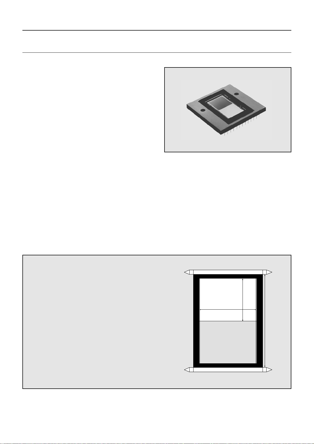
The FTT 1010-M is a monochrome progressive-scan frame-transfer
image sensor offering 1K x 1K pixels at 30 frames per second through
a single output buffer. The combination of high speed and a high
linear dynamic range (>12 true bits at room temperature without
cooling) makes this device the perf ect solution for high-end real time
medical X-ray, scientific and industrial applications. A second output
can either be used for mirrored images, or can be read out
simultaneously with the other output to double the frame rate. The
device structure is shown in figure 1.
Device structure
Optical size: 12.288 mm (H) x 12.288 mm (V)
Chip size: 14.572 mm (H) x 26.508 mm (V)
Pixel size: 12 µm x 12 µm
Active pixels: 1024 (H) x 1024 (V)
Total no. of pixels: 1072 (H) x 1030 (V)
Optical black pixels: Left: 20 Right: 20
Timing pixels: Left: 4 Right: 4
Dummy register cells: Left: 7 Right: 7
Optical black lines: Bottom: 6 Top: 6
Figure 1 - Device structure
1999 September 2
ZY
4
20
WX
Output
amplifier
7
6 black lines
Image Section
1024 active pixels
Storage Section
6 black lines
Output re
ister
1024
active
lines
4
20
2060
lines
71072 cells

Philips Semiconductors Product specification
Frame Transfer CCD Image Sensor FTT1010-M
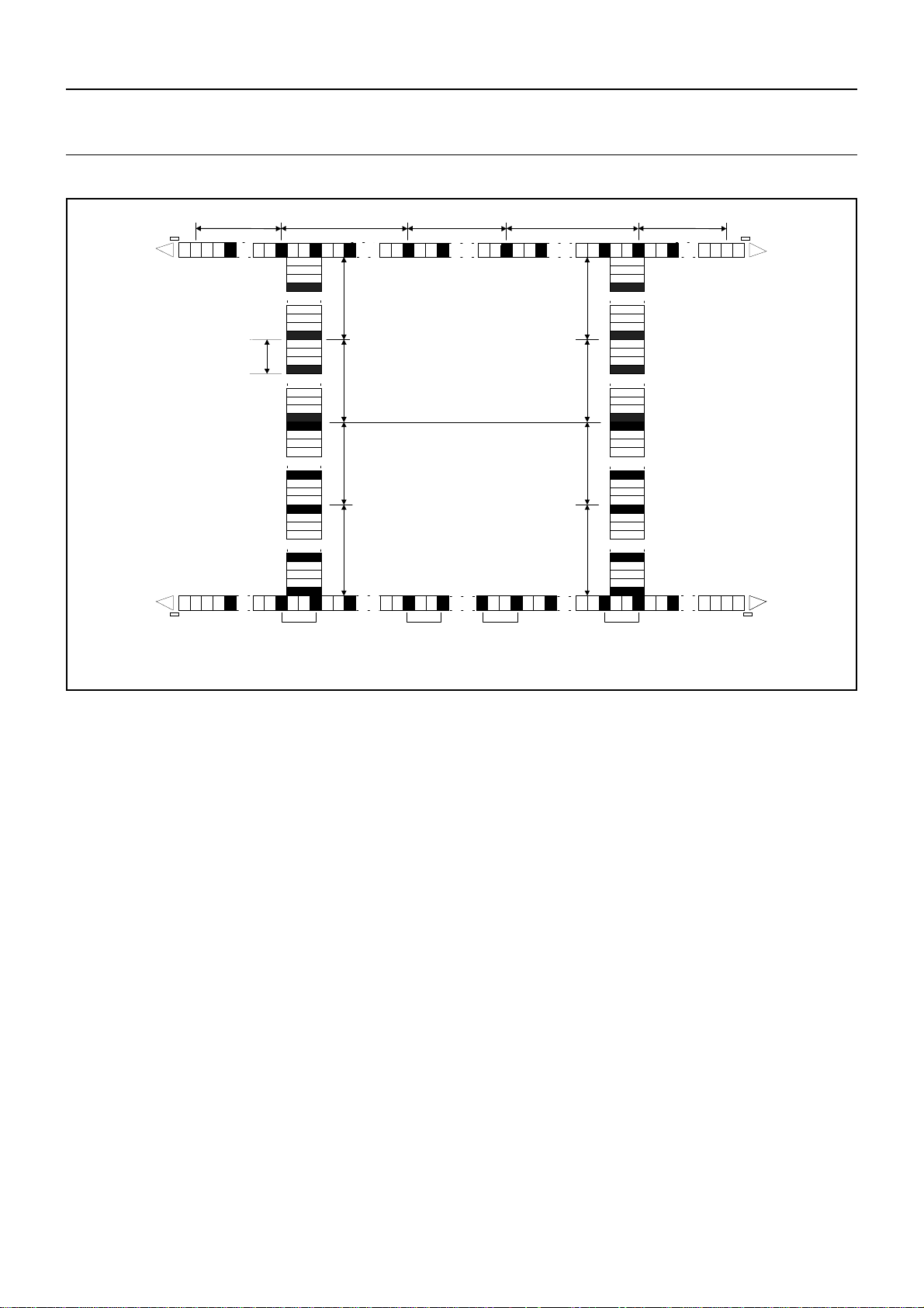
Architecture of the FTT1010-M
The FTT1010-M consists of a shielded storage section and an open
image section. Both sections are electronically the same and have
the same cell structure with the same properties. The only diff erence
between the two sections is the optical light shield.
The optical centres of all pixels in the image section form a square
grid. The charge is generated and integrated in this section. Output
registers are located below the storage section. The output amplifiers
Y and Z are not used in Frame Transfer mode and should be
connected as not-used amplifiers.
After the integration time the charge collected in the image section
is shifted to the storage section. The charge is read out line by line
through the lower output register.
IMAGE SECTION
The left and the right half of each output register can be controlled
independently. This enables either single or multiple read-out.
During vertical transpor t the C3 gates separate the pixels in the
register. The letters W, X, Y and Z are used to define the four
quadrants of the sensor. The central C3 gates of both registers are
part of the W and Z quadrants of the sensor.
Both upper and lower registers can be used for vertical binning.
Both registers also have a summing gate at each end that can be
used for horizontal binning. Figure 2 shows the detailed internal
structure.
Image diagonal (active video only)
Aspect ratio
Active image width x height
Pixel width x height
Geometric fill factor
Image clock pins
Capacity of each clock phase
Number of active lines
Number of black reference lines
Number of dummy black lines
Total number of lines
Number of active pixels per line
Number of overscan (timing) pixels per line
Number of black reference pixels per line
Total number of pixels per line
Storage width x height
Cell width x height
Storage clock phases
Capacity of each clock phase
Number of cells per line
Number of lines
17.38 mm
1:1
12.288 x 12.288 mm
12x12 µm
2
100%
A1, A2, A3, A4
2.5nF per pin
1024
2
4
1030
1024
8 (2x4)
40 (2x20)
1072
STORAGE SECTION
12.864 x 12.360 mm
12x12 µm
2
B1, B2, B3, B4
2.5nF per pin
1072
1030
2
2
OUTPUT REGISTERS
Output buffers (three-stage source foll ower)
Number of registers
Number of dummy cells per register
Number of register cells per register
Output register horizontal transport clock pins
Capacity of each C-clock phase
Overlap capacity between neighbouring C-clocks
Output register Summing Gates
Capacity of each SG
Reset Gate clock phases
Capacity of each RG
4 (one on each corner)
2 (one above, one below)
14 (2x7)
1072
C1, C2, C3
60pF per pin
20pF
4 pins (SG)
15pF
4 pins (RG)
15pF
1999 September 3
Philips Semiconductors Product specification
)
Frame Transfer CCD Image Sensor FTT1010-M
RD
RGRG
OUT_Z
(not used) (not used
SG: summing gate
OG: output gate
RG: reset gate
RD: reset dr ain
OUT_W
OG
SG
RG
RD
7 dummy
pixels
C3 C3 C3 C3 C3 C3 C3 C3 C3C3 C3
One Pixel
C3 C3 C3C3 C3 C3 C3C3 C3 C3 C3
20 black & 4
timing columns
C1C1SG C2OG C2 C2 C1 C2 C1 C2 C1 C2 C1 C2 C2C1 C1 C2 C1 C2 C1 C2 C1 C2 C1 SG OGC1 C3
A1 A1
A2
A3
A4
A1
A2
A3
A4
A1
A2
A3
A4
A1
A2
A3A3
A4
B2
B3
B4
A1
B1
B2
B3
B4
B1
B2
B3
B4
B1
B2
B3
B4
B1
C1C1C2 C2 C2 C1 C2 C1 C2C1 C3
column
1
6 black
lines
1K active
images lines
1K storage
lines
6 black lines
1K image 20 black & 4 timing
pixels
IMAGE
FT CCD
STORAGE
C1C2 C2 C1
C2 C1 C2 C2C1 C1
column
24 + 1
C3
column
24 + 1K
columns
A2
A3
A4
A1
A2
A3
A4
A1
A2
A3
A4
A1
A2
A3
A4
B1B1
B2
B3
B4
A1
B1
B2
B3
B4
B1
B2
B3
B4
B1
B2
B3
B4
B1
C2
C1
column
24 + 1K + 24
7 dummy
pixels
C1 C2
C1 SG
RD
OUT_Y
OUT_X
OG
RD
RG
RG
A1, A2, A3, A4: clocks of image section B1, B2, B3, B4: clocks of storage section C1, C2, C3: clocks of horizontal registers
Figure 2 - Detailed internal structure
1999 September 4
Philips Semiconductors Product specification
Frame Transfer CCD Image Sensor FTT1010-M
Specifications
ABSOLUTE MAXIMUM RATINGS
GENERAL:
storage temperature
ambient temperature during operation
voltage between any two gates
DC current through any clock phase (absolute value)
OUT current (no short circuit protection)
VOLTAGES IN RELAT ION TO VPS:
VNS, SFD, RD
VCS, SFS
all other pins
VOLTAGES IN RELAT ION TO VNS:
SFD, RD
VCS, SFS, VPS
all other pins
2
VNS
VPS
SFD
SFS
VCS
OG
RD
DC CONDITIONS
3
N substrate
P substrate
Source Follower Drain
Source Follower Source
Current Source
Output Gate
Reset Drain
1
MIN. MAX. UNIT
-55
-40
-20
-0.2
0
-0.5
-8
-5
-15
-30
-30
+80
+60
+20
+2.0
10
+30
+5
+25
+0.5
+0.5
+0.5
°C
°C
V
µA
mA
V
V
V
V
V
V
MIN. [V] TYPICAL [V] MAX . [V] MAX. [m A]
18
1
16
-
-5
4
13
24
3
20
0
0
6
15.5
28
7
24
3
8
18
15
15
4.5
1
-
-
-
AC CLOCK LEVEL CONDITIONS
2
MIN. TYPICAL MAX. UNIT
IMAGE CLOCKS:
A-clock amplitude during integration and hold
A-clock amplitude during vertical trans port (duty cycle=5/8)
A-clock low level
Charge Reset (CR) level on A-clock
5
4
8
10
-5
10
14
0
-5
V
V
V
V
STORAGE CLOCKS:
B-clock amplitude during hold
B-clock amplitude during vertical trans port (duty cycle=5/8)
8
10
10
14
V
V
OUTPUT REGISTER CLOCKS:
C-clock amplitude (duty cycle during hor. trans port = 3/6)
C-clock low level
Summing Gate (SG) amplitude
Summing Gate (SG) low level
4.75
2
5
3.5
10
3.5
5.25
10
V
V
V
V
OTHER CLOCKS:
Reset Gate (RG) amplitude
Reset Gate (RG) low level
Charge Reset (CR) pulse on Nsub
1
During Charge Reset it is allowed to exceed maximum rating levels (see note5).
2
All voltages in relation to SFS.
3
To set the VNS voltage for optimal Vertical Anti-Blooming (VAB), it should be adjustable between minimum and maximum values.
4
Three-level cloc k is preferred for maximum charge; the s wing during vertical transport should be 4V higher than the voltage during integration.
A two level clock (typically 10V) can be used if a lower maximum charge handling capacity is allowed.
5
Charge Reset can be achieved in two ways:
5
5
0
10
3
10
10
10
V
V
V
• The typical CR level is applied to all image clocks simultaneously (preferred).
• The typical A-clock low le vel is applied to all image cloc ks; f or proper CR, an additional Charge Reset pulse on VNS is required. This will also aff ect
the charge handling capacity in the storage areas.
1999 September 5
Philips Semiconductors Product specification
Frame Transfer CCD Image Sensor FTT1010-M
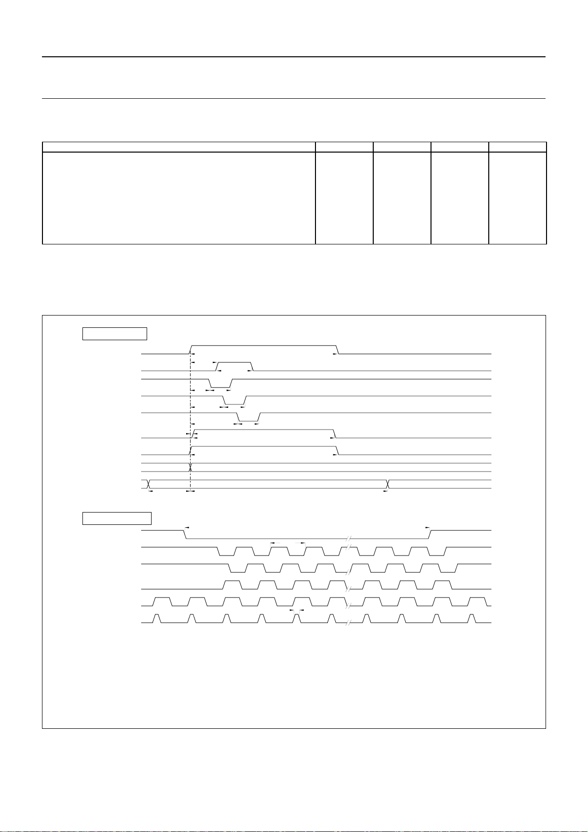
Timing diagrams (for default operation)
AC CHARACTERISTICS MIN. TYPICAL MAX. UNIT
Horizontal frequency (1/Tp)
Vertical frequency
Charge Reset (CR) time
Rise and fall times: image clocks (A)
1
Tp = 1 clock period
2
Duty cycle = 50% and phase shift of the C clocks is 120 degrees.
1
storage clocks (B)
register clocks (C)
summing gate (SG)
reset gate (RG)
0
0
2
10
2
10
3
3
3
18
450
5
20
20
5
5
5
40
1000
1/6 Tp
1/6 Tp
1/6 Tp
MHz
kHz
µs
ns
ns
ns
ns
ns
Line Timing
SSC
B1
B2
B3
B4
CR
AHigh
VD
BLC
Pixel Timing
SSC
C1
C2
C3
SG
RG
Tp = 1 clock period = 1 / 18MHz = 55.56ns
Pixel output sequence: 7 dumm y, 20 black, 4 timing, 1024 active, 4 timing, 20 black Line Time: 1184 x Tp = 65.7µs
* During AHigh = H the phiA high level is increased from 10V to 14V
H
L
H
L
H
L
H
L
H
L
H
L
H
*
L
H
L
H
L
30Tp
19Tp
14Tp
15Tp
24Tp
Tp2
34Tp
H
L
H
L
H
L
H
L
H
L
H
L
105Tp
25Tp
15Tp
15Tp
Tp101
Tp105
141Tp
1079 pixels
1Tp
Tp / 6
VD: Frame pulse
CR: Charge Reset
BLC: Black Level Clamp
B1 to B4: Vertical storage clocks
Figure 3 - Line and pixel timing diagrams
1999 September 6
C1 to C3: Horizontal register clocks
SSC: Start-Stop C-clocks
SG: Summing gate
RG: Reset gate
 Loading...