

Panasonic WJHD-500-B Service manual
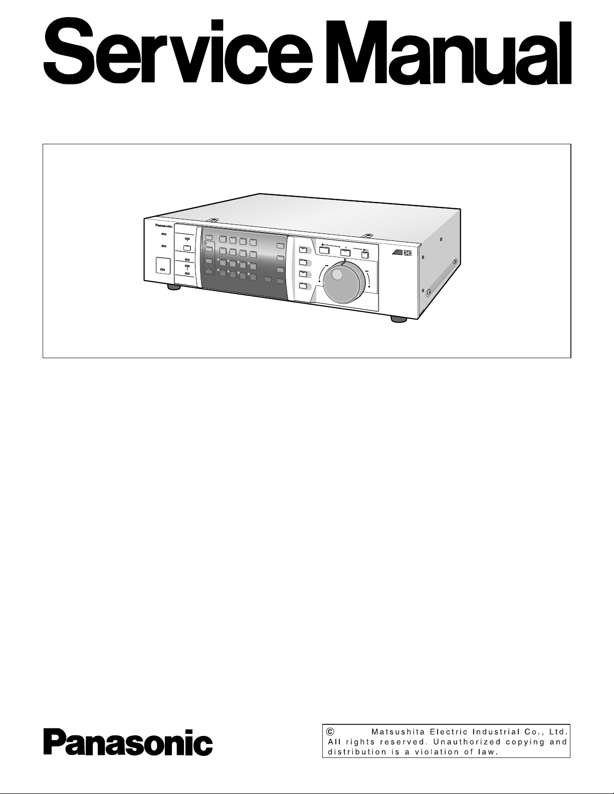
WJ-HD500B
ORDER NO. AVS0303489C8
Digital Disk Recorder
REMOTO
ALARM
GROUP
SELECT
PLAY PPAUSE
REV
FWD
INDEX
ALARM SEARCH
DISPLA
Y
ALARM
RESET
ALARM
SUSPEND
HDD
FULL
TIMER
OPRATE
Digital Disk
Recorder
WJ-HD
500
B
LOCK
SPOT
MULTISCREEN
MULTISCREEN
SELECT
EL-ZOOM
REC REVIEW
REC STOP
1
2
3
4
5
6
7
8
9
10
11
12
13
14
15
16
SET
+
-
FS
16
SPECIFICATIONS
General
Power Source : 220 - 240 V AC, 50 Hz
Power Consumption : 55 W
Ambient Operating Temperature : +5°C - +45°C (41°F - 113°F)
Ambient Operating Humidity : Less than 85 %
Dimensions : 420 mm (W) x 88 mm (H) x 350 mm (D) [16-9/16” (W) x 3-7/16” (H) x 13-3/4” (D)]
Weight : 8 kg (17.6 lbs.)
Input and Output
Video Input : 1.0 V[p-p] / 75 Ω Composite video signal with 75 ΩAutomatic Termination / Looping through (x16)
Video Output : 1.0 V[p-p] / 75 Ω Composite video signal / Looping through (x16)
Spot Output : 1.0 V[p-p] / 75 Ω Composite video signal (x1)
Multiscreen Output : 1.0 V[p-p] / 75 Ω Composite video signal (x1)
Gen-lock Output : Black burst signal 0.43 V[p-p] / 75 Ω
Audio Input : –10 dB unbalanced, RCA standard jack
Audio Output : –10 dB unbalanced, RCA standard jack
Extension Storage Port : SCSI Interface 50-pin Half Pitch D-sub connector (x1)
Copy Port : SCSI Interface 50-pin Half Pitch D-sub connector (x1)
Control Port : 25-pin Full Pitch D-sub connector (x1)
Alarm Port : 25-pin Full Pitch D-sub connector (x1)
Data Port : RS-485 6-conductor modular jack (RJ-11)
Remote Port : For Exclusive Remote Controller, serial interface (RJ-11)
Serial Port : RS-232C 9-pin Full Pitch D-sub connector
10/100BASE-T Port : 10Base-T and 100Base-TX, 8-conductor modular jack (RJ-45)
(Installed Optional Network Board)
Weight and dimensions shown are approximate.
Specifications are subject to change without notice.
2003
This service information is designed for experienced repair technicians only and is not designed for use by the
general public.
It does not contain warnings or cautions to advise non-technical individuals of potential dangers in attempting to
service a product.
Products powered by electricity should be serviced or repaired only by experienced professional technicians. Any
attempt to service or repair the product or products dealt with in this service information by anyone else could
result in serious injury or death.
Y
WARNING
STANDARD ACCESSORIES
AC Power Cord ......................................................... 2 pc.
Rack Mounting Bracket ............................................. 2 pcs.
Screw for Rack Mounting Bracket (M4x10) ............... 4 pcs.
Absorber .................................................................... 4 pcs.
Sleeve ....................................................................... 4 pcs.
Earth Lug ................................................................... 1 pc.
Hard Disk Fixing Screw ............................................. 4 pcs.
CAUTION
RISK OF ELECTRIC SHOCK
DO NOT OPEN
CAUTION:
TO REDUCE THE RISK OF ELECTRIC SHOCK,
DO NOT REMOVE COVER (OR BACK). NO USER
SERVICEABLE PARTS INSIDE.
REFER SERVICING TO QUALIFIED SERVICE
PERSONNEL.
IMPORTANT SAFETY NOTICE
There are special components used in this equipment which are important for safety. These parts are indicated
by the ” Y ” mark on the schematic diagram and the replacement parts list. It is essential that these critical
parts should be replaced with manufacturer's specified parts to prevent X-radiation, shock, fire, or other hazards.
Do not modify the original design without permission of manufacture.
This symbol warns the user that uninsulated voltage within
the unit may have sufficient magnitude to cause electric
shock. Therefore, it is dangerous to make any kind of contact
with any inside part of this unit.
This symbol alerts the user that important literature concerning
the operation and maintenance of this has been included.
Therefore, it should be read carefully in order to avoid
any problems.
Warning
The lithium battery in this equipment must only be
replaced by qualified personnel. When necessary,
contact your local Panasonic supplier.
CAUTION
Danger of explosion if battery is incorrectly replaced.
Replace only with the same or equivalent type recommended
by the equipment manufacturer. Discard used batteries
according to manufacturer's instructions.

CONTENTS
Major Operating Controls and Their Functions . . . . . . . . . . . . . . . . . . . . . . . . . . . . . . . . . . . . . . . . . . . . . . . . 1-1
DIP Switch Setting . . . . . . . . . . . . . . . . . . . . . . . . . . . . . . . . . . . . . . . . . . . . . . . . . . . . . . . . . . . . . . . . . . . . . . . . 2-1
Adjustment Procedure . . . . . . . . . . . . . . . . . . . . . . . . . . . . . . . . . . . . . . . . . . . . . . . . . . . . . . . . . . . . . . . . . . . . . 2-2
Location of Test Points and Adjusting Controls . . . . . . . . . . . . . . . . . . . . . . . . . . . . . . . . . . . . . . . . . . . . . . . 2-8
Wiring Diagram . . . . . . . . . . . . . . . . . . . . . . . . . . . . . . . . . . . . . . . . . . . . . . . . . . . . . . . . . . . . . . . . . . . . . . . . . . . 3-1
Block Diagram
Main Board (1/10) . . . . . . . . . . . . . . . . . . . . . . . . . . . . . . . . . . . . . . . . . . . . . . . . . . . . . . . . . . . . . . . . . . . . . . . 3-2
Main Board (2/10) . . . . . . . . . . . . . . . . . . . . . . . . . . . . . . . . . . . . . . . . . . . . . . . . . . . . . . . . . . . . . . . . . . . . . . . 3-3
Main Board (3/10) . . . . . . . . . . . . . . . . . . . . . . . . . . . . . . . . . . . . . . . . . . . . . . . . . . . . . . . . . . . . . . . . . . . . . . . 3-4
Main Board (4/10)/(5/10) . . . . . . . . . . . . . . . . . . . . . . . . . . . . . . . . . . . . . . . . . . . . . . . . . . . . . . . . . . . . . . . . . . 3-5
Main Board (6/10)/Rear Board . . . . . . . . . . . . . . . . . . . . . . . . . . . . . . . . . . . . . . . . . . . . . . . . . . . . . . . . . . . . . . 3-6
Main Board (7/10) . . . . . . . . . . . . . . . . . . . . . . . . . . . . . . . . . . . . . . . . . . . . . . . . . . . . . . . . . . . . . . . . . . . . . . . 3-7
Main Board (8/10)/(9/10)/BNC Board . . . . . . . . . . . . . . . . . . . . . . . . . . . . . . . . . . . . . . . . . . . . . . . . . . . . . . . . . 3-8
Main Board (8/10)/(10/10) . . . . . . . . . . . . . . . . . . . . . . . . . . . . . . . . . . . . . . . . . . . . . . . . . . . . . . . . . . . . . . . . . 3-9
Analog Board . . . . . . . . . . . . . . . . . . . . . . . . . . . . . . . . . . . . . . . . . . . . . . . . . . . . . . . . . . . . . . . . . . . . . . . . . 3-10
Front Board/LED Board . . . . . . . . . . . . . . . . . . . . . . . . . . . . . . . . . . . . . . . . . . . . . . . . . . . . . . . . . . . . . . . . . 3-11
Motion Detector Board . . . . . . . . . . . . . . . . . . . . . . . . . . . . . . . . . . . . . . . . . . . . . . . . . . . . . . . . . . . . . . . . . . . 3-12
Schematic Diagram
Main Board (1/10) . . . . . . . . . . . . . . . . . . . . . . . . . . . . . . . . . . . . . . . . . . . . . . . . . . . . . . . . . . . . . . . . . . . . . . . 4-1
Main Board (2/10) . . . . . . . . . . . . . . . . . . . . . . . . . . . . . . . . . . . . . . . . . . . . . . . . . . . . . . . . . . . . . . . . . . . . . . . 4-2
Main Board (3/10) . . . . . . . . . . . . . . . . . . . . . . . . . . . . . . . . . . . . . . . . . . . . . . . . . . . . . . . . . . . . . . . . . . . . . . . 4-3
Main Board (4/10) . . . . . . . . . . . . . . . . . . . . . . . . . . . . . . . . . . . . . . . . . . . . . . . . . . . . . . . . . . . . . . . . . . . . . . . 4-4
Main Board (5/10) . . . . . . . . . . . . . . . . . . . . . . . . . . . . . . . . . . . . . . . . . . . . . . . . . . . . . . . . . . . . . . . . . . . . . . . 4-5
Main Board (6/10) . . . . . . . . . . . . . . . . . . . . . . . . . . . . . . . . . . . . . . . . . . . . . . . . . . . . . . . . . . . . . . . . . . . . . . . 4-6
Main Board (7/10) . . . . . . . . . . . . . . . . . . . . . . . . . . . . . . . . . . . . . . . . . . . . . . . . . . . . . . . . . . . . . . . . . . . . . . . 4-7
Main Board (8/10)/BNC Board . . . . . . . . . . . . . . . . . . . . . . . . . . . . . . . . . . . . . . . . . . . . . . . . . . . . . . . . . . . . . . 4-8
Main Board (9/10) . . . . . . . . . . . . . . . . . . . . . . . . . . . . . . . . . . . . . . . . . . . . . . . . . . . . . . . . . . . . . . . . . . . . . . . 4-9
Main Board (10/10) . . . . . . . . . . . . . . . . . . . . . . . . . . . . . . . . . . . . . . . . . . . . . . . . . . . . . . . . . . . . . . . . . . . . . 4-10
Analog Board (1/2) . . . . . . . . . . . . . . . . . . . . . . . . . . . . . . . . . . . . . . . . . . . . . . . . . . . . . . . . . . . . . . . . . . . . . . 4-11
Analog Board (2/2) . . . . . . . . . . . . . . . . . . . . . . . . . . . . . . . . . . . . . . . . . . . . . . . . . . . . . . . . . . . . . . . . . . . . . . 4-12
Rear Board (1/2) . . . . . . . . . . . . . . . . . . . . . . . . . . . . . . . . . . . . . . . . . . . . . . . . . . . . . . . . . . . . . . . . . . . . . . . 4-13
Rear Board (2/2) . . . . . . . . . . . . . . . . . . . . . . . . . . . . . . . . . . . . . . . . . . . . . . . . . . . . . . . . . . . . . . . . . . . . . . . 4-14
Front Board/LED Board . . . . . . . . . . . . . . . . . . . . . . . . . . . . . . . . . . . . . . . . . . . . . . . . . . . . . . . . . . . . . . . . . . 4-15
Power Board . . . . . . . . . . . . . . . . . . . . . . . . . . . . . . . . . . . . . . . . . . . . . . . . . . . . . . . . . . . . . . . . . . . . . . . . . . 4-16
Motion Detector Board (1/2) . . . . . . . . . . . . . . . . . . . . . . . . . . . . . . . . . . . . . . . . . . . . . . . . . . . . . . . . . . . . . . . 4-17
Motion Detector Board (2/2) . . . . . . . . . . . . . . . . . . . . . . . . . . . . . . . . . . . . . . . . . . . . . . . . . . . . . . . . . . . . . . . 4-18
Conductor View
Main Board (Component Side View)/BNC Board . . . . . . . . . . . . . . . . . . . . . . . . . . . . . . . . . . . . . . . . . . . . . . . 5-1
Main Board (Pattern Side View) . . . . . . . . . . . . . . . . . . . . . . . . . . . . . . . . . . . . . . . . . . . . . . . . . . . . . . . . . . . . . 5-2
Analog Board . . . . . . . . . . . . . . . . . . . . . . . . . . . . . . . . . . . . . . . . . . . . . . . . . . . . . . . . . . . . . . . . . . . . . . . . . . . 5-3
Rear Board . . . . . . . . . . . . . . . . . . . . . . . . . . . . . . . . . . . . . . . . . . . . . . . . . . . . . . . . . . . . . . . . . . . . . . . . . . . . . 5-4
Power Board . . . . . . . . . . . . . . . . . . . . . . . . . . . . . . . . . . . . . . . . . . . . . . . . . . . . . . . . . . . . . . . . . . . . . . . . . . . 5-5
Front Board/LED Board . . . . . . . . . . . . . . . . . . . . . . . . . . . . . . . . . . . . . . . . . . . . . . . . . . . . . . . . . . . . . . . . . . . 5-6
Motion Detector Board . . . . . . . . . . . . . . . . . . . . . . . . . . . . . . . . . . . . . . . . . . . . . . . . . . . . . . . . . . . . . . . . . . . . 5-7
Exploded View . . . . . . . . . . . . . . . . . . . . . . . . . . . . . . . . . . . . . . . . . . . . . . . . . . . . . . . . . . . . . . . . . . . . . . . . . . . . 6-1
Replacement Parts List . . . . . . . . . . . . . . . . . . . . . . . . . . . . . . . . . . . . . . . . . . . . . . . . . . . . . . . . . . . . . . . . . . . . 7-1
– 1-1 –
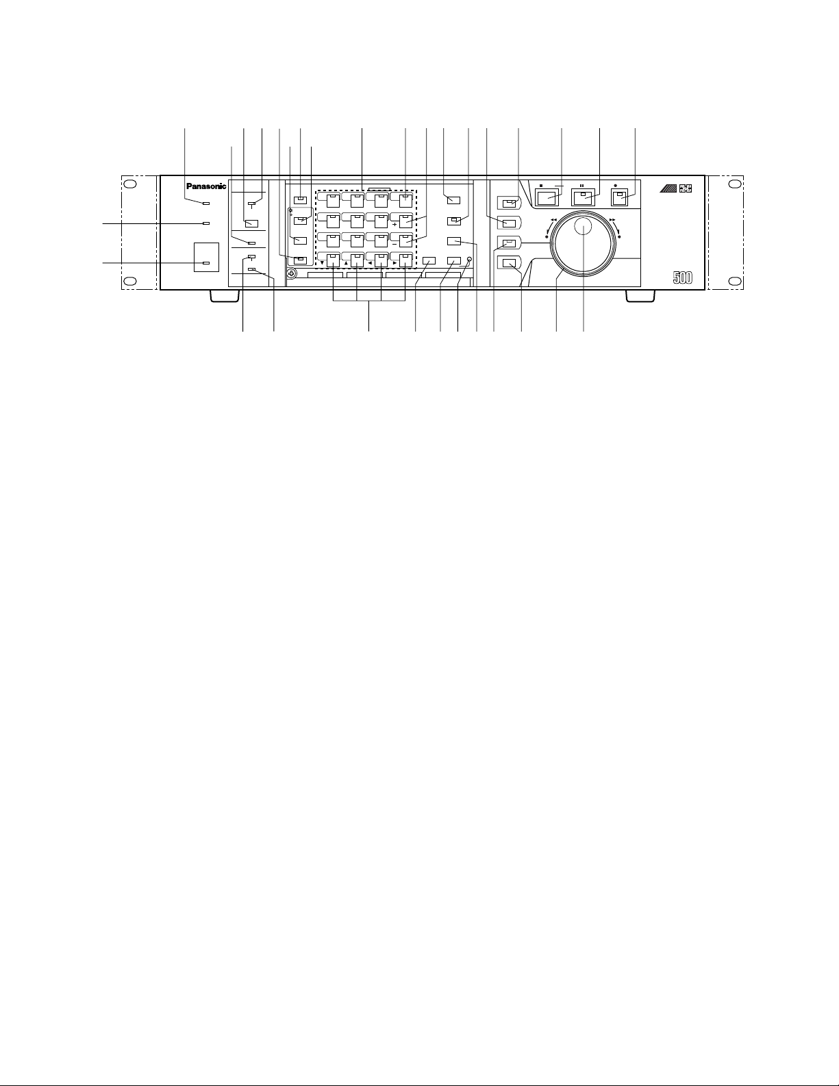
MAJOR OPERATING CONTROLS AND THEIR FUNCTIONS
REMOTE
TIMER
OPERATE
FULL
HDD
SEQUENCE
SET
LOCK
ALARM
ALARM
RESET
ALARM
SUSPEND
MULTISCREEN
SELECT
SETUP
/ESC
GROUP
SELECT
SPOT
MULTISCREEN
DAYLIGHT SAVINGS
EL-ZOOM
COPY
REC PREVIEW
INDEX
STOP BPLAY/ PAUSE REC
FWDREV
ALARM SEARCH
DISPLAY
REC STOP
1 2 3 4
13 14 15 16
9 10 11 12
5 6 7 8
Digital Disk
Recorder
WJ-HD B
FS
16
q
w
etyu!0 !1
rio
!3
!4 !5 !6 !7 !8 !9 @0
!2
@1@3@4@5@6 @2@7@8@9#0#1
q Operate Indicator (OPERATE)
Is on when the power of the WJ-HD500B Digital Disk
Recorder is turned on.
w Timer Indicator (TIMER)
Lights to indicate when the TIMER is set to INT (internal
timer) in the setup menu.
e Remote Indicator (REMOTE)
Lights to indicate when the Disk Recorder is controlled
by an outboard device via the Serial or 10/100BASE-T
port on the rear of the Disk Recorder.
r Alarm Suspend Indicator (ALARM SUSPEND)
Lights to indicate that the alarm suspension mode is
selected.
t Alarm Reset Button (ALARM RESET)
This button cancels an activated alarm.
Pressing this button will reset the alarm and return the
system to the condition before the alarm function was
activated.
y Alarm Indicator (ALARM)
This indicator blinks to indicate that an alarm condition
exists.
It changes to a steady light when the alarm is reset automatically.
To turn the indicator off, press the ALARM RESET button.
u Sequence Button (SEQUENCE)
Runs the assigned sequence on the selected monitor
screen for the specified duration.
During the sequence, pressing this button will pause the
sequence that is being run on the monitor screen.
The LED indicates the status as follows.
On: Sequence is being run.
Blinking: Sequence is in pause mode.
i Multiscreen Selection Button
(MULTISCREEN SELECT)
Selects the multiscreen pattern to be displayed on the
Multiscreen Monitor that is connected to the MULTI
SCREEN OUT on the rear of the Recorder.
Pressing this button will toggle the display on the monitor screen as shown below.
4 → 7 → 9 → 10 → 13 → 16 → 4 screen segments
o Monitor Selection Button (SPOT / MULTISCREEN)
Selects to control the display on the screen for either the
Spot or Multiscreen Monitor.
Pressing this button will toggle the indicator in the button
on and off to indicate the selected monitor as shown
below.
On: Indicates the Spot monitor is selected.
Off: Indicates the Multiscreen monitor is selected.
!0 Lock Button (LOCK)
Toggles to enable or disable the button lock function on
both front panels of the Disk Recorder and Remote
Controller.
The LED indicates the status as shown below.
On: The button lock is enabled.
Off: The button lock is disabled.
While On, the button lock will be released only if the preset password is entered in the password inquiry window.
!1 Numeric Buttons (1 - 16)
These buttons are used for numeric input into the system such as the video selection, password, etc.
The indicator in the button lights up to indicate as shown
below.
Green: The input is displayed on the monitor.
Yellow: The input is displayed on the monitor and
recorded on the Hard Disk.
Orange: The input is recorded on the Hard Disk (no dis-
play).
■ Front View

– 1-2 –
!2 Set Button (SET)
During the setup, this button is used to display a submenu in the setup menu if the item has its own setting
menu.
!3 Increment /Decrement Button (+, -)
These buttons are used to zoom in and out the zoomed
image presently displayed on the Multiscreen Monitor.
During the setup, these buttons are used to select the
item parameter in the setup menu.
!4 Recording Stop Button (REC STOP)
Pressing this button will stop the recording.
!5 Recording Preview Button (REC PREVIEW)
Use this button to display the playback image with the
live images on the Multiscreen Monitor.
The LED indicates the status as shown below.
On: The selected playback image is displayed
Blinking: Prompts you to select the numeric button for
displaying the playback image.
!6 Index Button (INDEX)
Displays the all record list (list and thumbnail) or alarm
and emergency list depending on the status of the
ALARM SEARCH button.
!7 Group Selection Button (GROUP SELECT)
Selects the camera group from among group 1, 2, 3 and
4.
The LED will light while any of the groups is selected.
!8 Stop Button (STOP)
Pressing this button will stop the playback.
!9 Playback / Pause Button (PLAY/PAUSE)
Pressing this button will start the playback.
During playback, pressing this button will pause the
playback.
The indicator in the button lights to indicate as shown
below.
On: Indicates that the playback mode is selected.
Blinking: Indicates that the pause mode is selected.
@0 Record Button (REC)
Pressing this button will start the recording manually
when the Timer parameter is set to OFF in the setup
menu.
The indicator in the button lights up to indicate that the
recording mode is selected.
@1 JogDial
Rotate in paused playback to move forward or backward
to the next recorded image.
It is also used to select the recording number when the
recorded list is displayed on the monitor.
@2 Shuttle Ring
Rotate in playback or paused playback to search the
recorded images forward or backward at variable speed.
@3 Display Button (DISPLAY)
Pressing this button will display the recording list with
the search editing area to find the record to be played
back.
@4 Alarm Search Button (ALARM SEARCH)
Selects either the list of alarm (REC+ALM) and emergency recordings or all recordings to be displayed on the
Multiscreen Monitor.
The LED indicates the status of selection as shown
below.
On: Search records for alarm (REC+ALM) and emer-
gency recordings.
Off: Search records for all recordings.
@5 Electronic Zoom Button (EL-ZOOM)
This button is used to zoom an image presently displayed in a single spot on the Multiscreen Monitor.
@6 Daylight Savings Button (DAYLIGHT SAVINGS)
The DAYLIGHT SAVINGS button is recessed inside the
front panel opening. Pressing this button will shift the
internal clock to the summer time or vice versa.
@7 Copy Button (COPY)
Copies the selected images on to the DVD-RAM disk
when the system is equipped the DVD Extension Unit.
@8 Setup / Escape Button (SETUP/ESC)
This button is used in the Disk Recorder’s Setup operation. Pressing this button for two seconds or more will
open the Disk Recorder’s Setup menu on the screen of
the Multiscreen Monitor. During the setup, press this button to return to the previous setup menu.
@9 Direction Buttons (CDA B)
These buttons are used to select an area for a zoomed
image displayed on the Multiscreen Monitor.
During the setup, these buttons are used to move the
cursor position in the setup menu of the Disk Recorder.
C: Downward
D: Upward
A: Left
B: Right
#0 Full Indicator (FULL)
Lights to indicate when the available recording space of
the Disk Recorder (HDD) is running low.
#1 Hard Disk Drive Indicator (HDD)
Lights to indicate when the Hard Disk is activated.
– 1-3 –
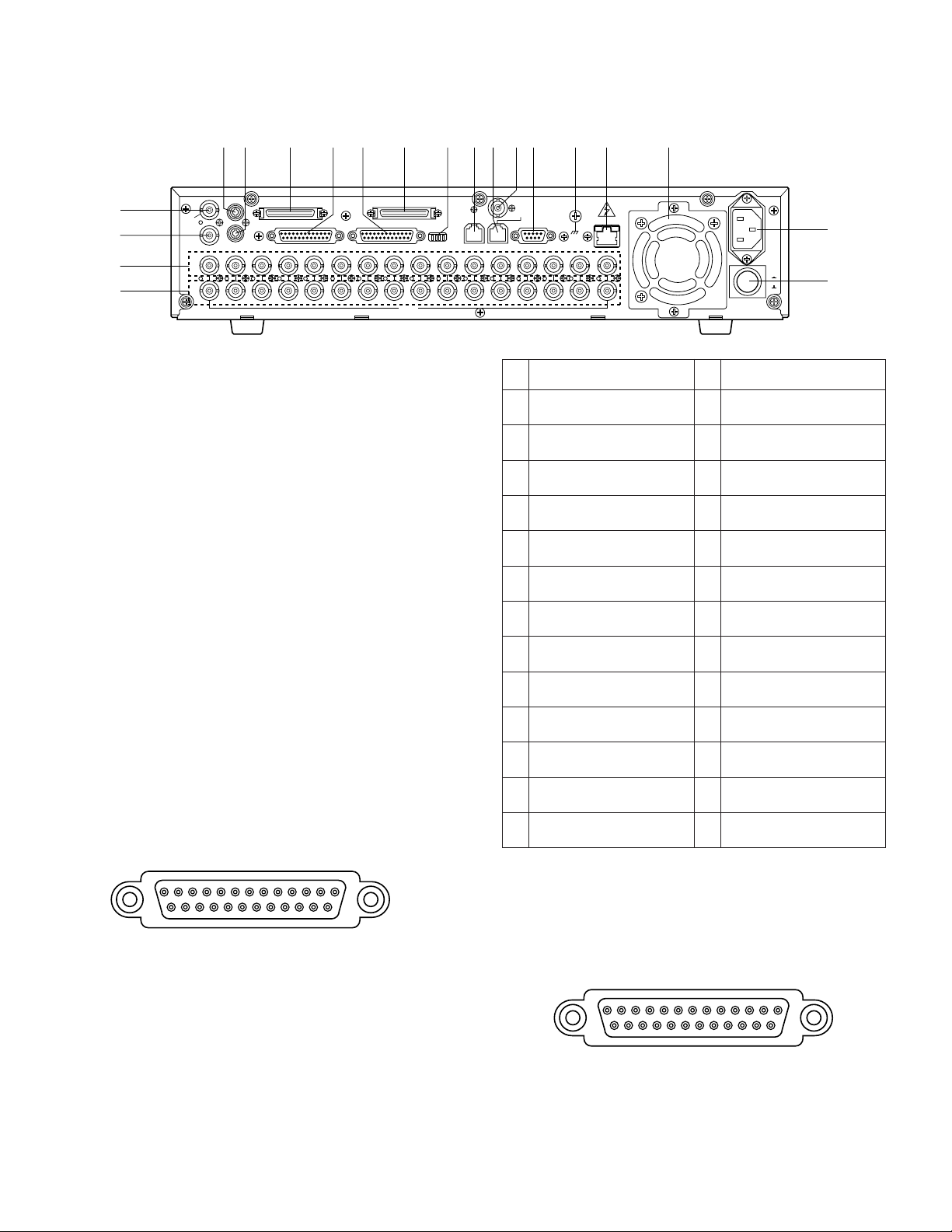
16161515141413131212111110109988776655443 2231
1
SIGNAL GND
10/100
BASE-T
SPOT
OUT
IN EXT STORAGE COPY
CONTROL ALARM
VIDEO
MODE
DATA
REMOTE(WV-CU50)
GEN-LOCK OUT
SERIAL
POWER
ON
AC
IN
OFF
IN
OUT
OUT
MULTI SCREEN OUT
AUDIO
$1
^0
$2
%9
$3 $4 $5 $6 $7 $8 $9 %0 %1 %2%3 %4 %5 %6
%7
%8
■ Rear View
$1 Multiscreen Output Connector (MULTI SCREEN
OUT)
The video output signal for the Multiscreen Monitor is
provided via this connector.
It can be displayed as the video input in a multiscreen
mode (4, 7, 9, 10, 13,16 screen segments).
It also displays the Recorder’s playback images.
Pressing the SETUP/ESC button for two seconds or
more will automatically select the Multiscreen Monitor
and display the Disk Recorder’s Setup menu.
$22 Spot Output Connector (SPOT OUT)
The video output signal for the Spot Monitor is provided
via this connector.
Displaying the Disk Recorder’s playback is disabled.
$3 Audio Input Connector (AUDIO IN)
For audio input from an external device, if applicable.
$4 Audio Output Connector (AUDIO OUT)
For audio output to an external device, if applicable.
$5 Extension Storage Port (EXT STORAGE)
For connecting the optional Extension Unit.
$6 Control Port (CONTROL)
The port has the functions listed below. Make connections to these pins as needed for operating your system.
The pin assignment of the port is shown below.
$7 Alarm Port (ALARM)
This port accepts the alarm input from the associated
alarm sensors through either Normally Open or Normally
Closed contacts.
The pin assignment of the port is shown below.
CONTROL
1
13
14
25
Designation
Pin
No.
1
2
3
4
5
6
7
8
9
10
11
12
13
Group Recording Output
Manual Recording Output
Emergency Recording
Output
Sequence Timing Output
DVD Remain Space
Output
HDD Remain Space
Output
Thermal Error Input
(Extension 1)
Thermal Error Input
(Extension 2)
Thermal Error Input
(Extension 3)
Thermal Error Input
(Extension 4)
Thermal Error Input
(Extension 5)
Thermal Error Input
(Extension 6)
Thermal Error Input (DVD
Unit)
Pin
No.
14
15
16
17
18
19
20
21
22
23
24
25
Designation
Disk Recorder Error
Output
Ground
Ground
Power Failure Detect Input
Power Failure Proceeding
Output
Power Failure Process
Completion Output
Ground
Emergency Recording
Input
Time Adjustment Output
Daylight Savings Select
Time Adjustment Input
Ground
1
14
13
25
ALARM

– 1-4 –
$8 Copy Port (COPY)
For connecting the optional DVD Extension Unit.
$9 Mode Selector (MODE)
Selects data termination for PS
•
Data system expansion.
%0 Data Port (DATA)
Exchanges control data with the external device with
PS
•
Data (Panasonic Security Data) mode.
%1 Remote Port [REMOTE (WV-CU50)]
This port is provided for controlling the Disk Recorder
with the optional WV-CU50 Remote Controller.
To connect to the controller, use a 6-conductor modular
cable supplied as an accessory with the controller.
%2 Gen-lock Output Connector (GEN-LOCK OUT)
This connector is used to connect an external system for
synchronization.
To record images at maximum recording rate, for example 50 fps, connect this output to the cameras to synchronize the system.
%3 Serial Port (SERIAL)
For connecting a Personal Computer.
%4 Signal Ground Terminal (SIGNAL GND)
%5 10/100BASE-T Port (Optional)
An optional Network Board can be installed in the Disk
Recorder.
This port is used to exchange control data with Ethernet
via an Ethernet Hub.
%6 Cooling Fan
Prevents the temperature of the Recorder from rising,
Do not block the ventilation opening on the cover.
%7 AC Inlet Socket (AC IN)
Plug the power cord (supplied as a standard accessory)
into this socket and connect it to an AC outlet.
%8 Power Switch (POWER ON/OFF)
This switch turns the power of the Disk Recorder on and
off.
%9 Video Output Connectors (VIDEO OUT 1 - 16)
The video signal connected to the Video Input
Connector (VIDEO IN) is looped through these connectors with an automatic 75 Ω termination.
^0 Video Input Connectors (VIDEO IN 1 - 16)
These connectors accept either a colour or B/W composite video signal from the camera.
Pin
No.
Designation
1
2
3
4
5
6
7
8
9
10
11
12
13
Alarm Input 1
Alarm Input 2
Alarm Input 3
Alarm Input 4
Sequence Timing Input
Alarm Reset Output
Ground
Alarm Recover Input
Alarm Output
Alarm Input 10
Alarm Input 11
Alarm Input 12
Alarm Input 13
Pin
No.
14
15
16
17
18
19
20
21
22
23
24
25
Designation
Ground
Alarm Input 5
Alarm Input 6
Alarm Input 7
Alarm Input 8
Alarm Input 9
Ground
+5 V Output (0.2 A)
Recording Timer Select
Input
Alarm Input 14
Alarm Input 15
Alarm Input 16
– 2-1 –
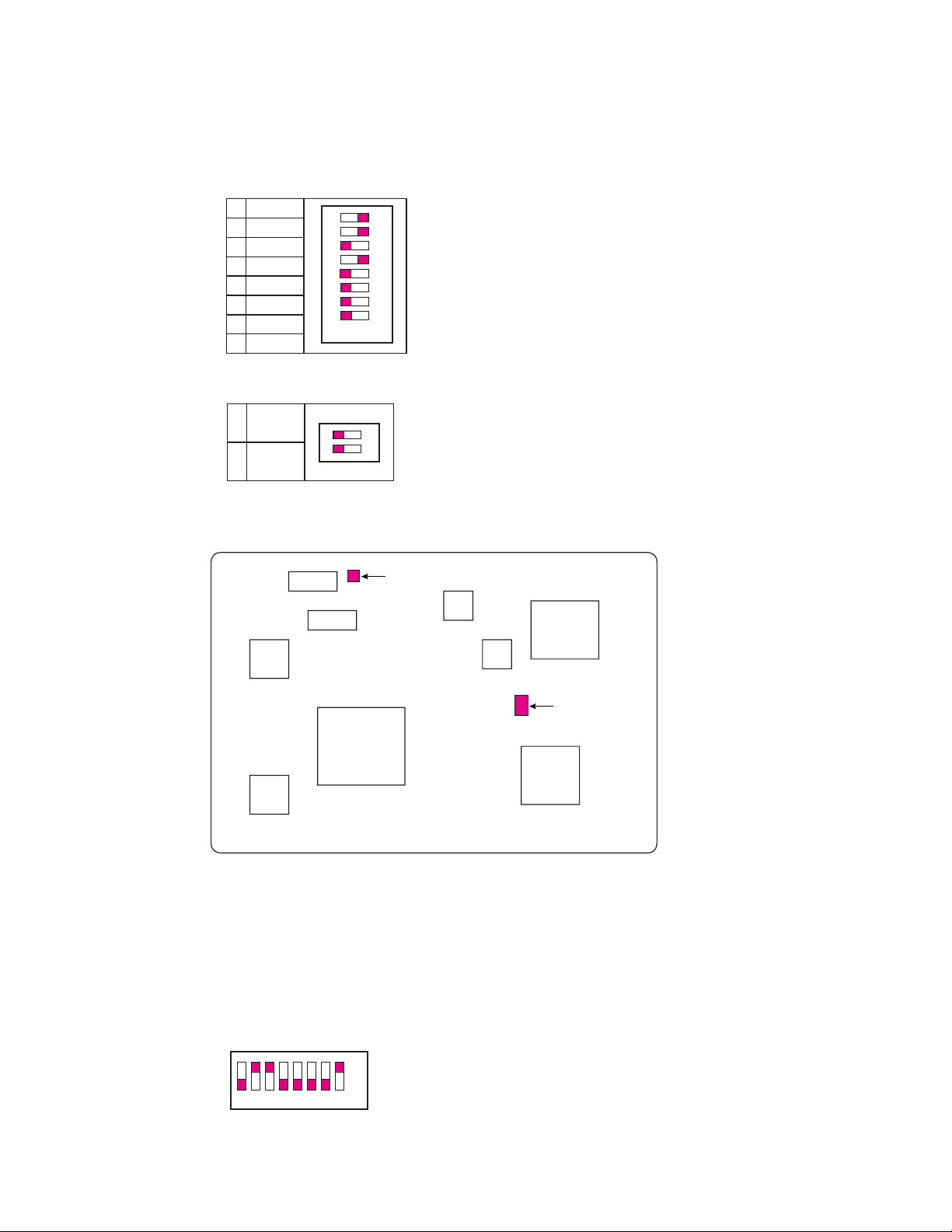
DIP SWITCH SETTING
SW23 SETTING
Fig. 1
Fig. 2
SW1 SETTING
1 ON
2 ON
3 OFF
4 ON
5 OFF
6 OFF
7 OFF
8 OFF
SW400 SETTING
1 OFF
2 OFF
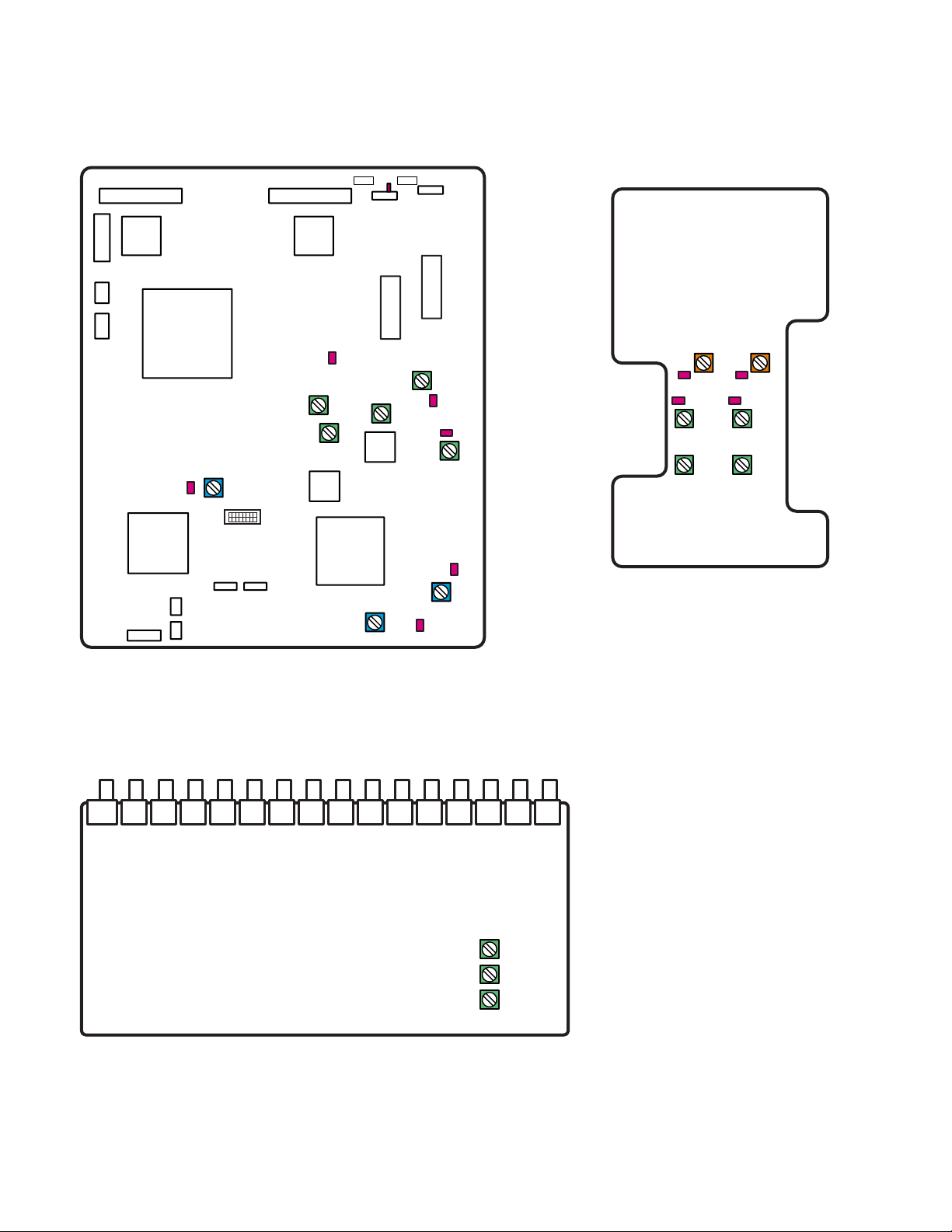
SWITCH LOCATION
Rear Side
Front Side
Main Board
SW400
SW23
O
N
O
N
1
2
3
4
5
6
7
8
1
2
12345678
ON
OFF
SCSI-IDE BOARD
MAIN BOARD
8 When replacing the SCSI-IDE Board, confirm that the #2, #3 and #8 of Dip Switch (SW1) on the SCSI-IDE Board
are set to ON position as shown in Fig. 2.
8 When replacing the Main Board Ass'y or Dip Switches on the Main Board, set SW23 and SW400 as shown in Fig. 1.
– 2-2 –
ADJUSTMENT PROCEDURE
1. Test Equipments Required
8
The following Test Equipments are required for adjustment of the Digital Disk Recorder WJ-HD500B.
8
Digital Voltmeter
8
Frequency Counter
8
Oscilloscope
8
Underscanned Colour Video Monitor
8
Video Signal Generator (Colour Bar Signal)
8
Ceramic Screwdriver
8
Extension Cable A (Part No. : V0EA1311AN) as shown in
Fig. 1-1.
Fig 1-1
8
Extension Cable B (Part No. : V0JA0010AN) as shown in
Fig. 1-2.
Fig 1-2
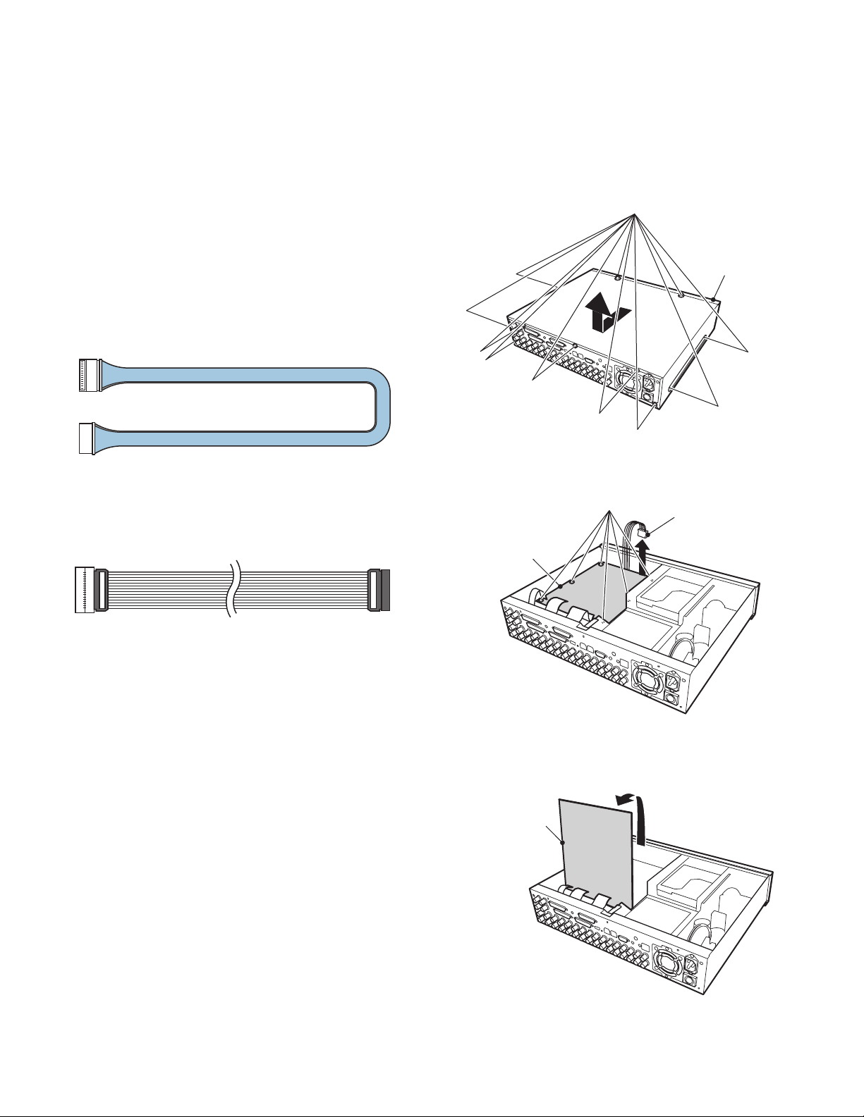
2. Disassembling Procedure for
Adjustment
8
Referring to Fig. 2-1, remove eleven screws that secure
the Top Cover and remove the Top Cover.
Fig. 2-1
8
Referring to Fig. 2-2, remove six screws that secure the
Main Board and disconnect CN403 on the Main Board.
Fig. 2-2
8
Referring to Fig. 2-3, turn over the Main Board with the
front side up.
Fig 2-3
To Front Board CN403
To Main Board CN403
Remove eleven screws.
Top Cover
Remove six screws.
Main Board
CN403
Analog Board CN501 Motion Detector Board CN601
Analog Board CN502 Motion Detector Board CN101
Main Board
– 2-3 –
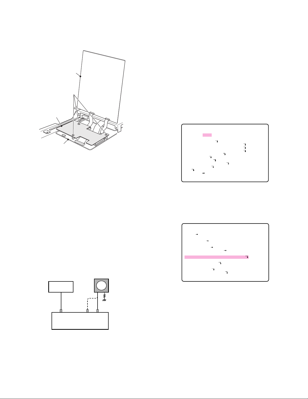
8
Referring to Fig. 2-4, remove three screws that secure the
Motion Detector Board and remove the Motion Detector
Board.
Fig 2-4
8
Connect the Extension Cable A between CN403 on the
Main Board and CN403 on the Front Board.
8
Connect the Extension Cable B between CN501 on the
Analog Board and CN601 on the Motion Detector Board.
8
Connect the Extension Cable B between CN502 on the
Analog Board and CN101 on the Motion Detector Board.
3. Connection and Setting Up for
Adjustment
3.1. Connection
8
Fig. 3-1 shows the connecting diagram for adjustment of
the WJ-HD500B.
Fig 3-1
8
Connect the Underscanned Colour Video Monitor to the
Multiscreen Output Connector or Gen-lock Output
Connector on the Rear Panel of the WJ-HD500B.
8
Terminate the input terminal of the Underscanned Colour
Video Monitor with 75 Ω.
8
Connect the Video Signal Generator to the Video Input
Connector on the Rear Panel of the WJ-HD500B.
8
Connect the probe of the Oscilloscope, the Frequency
Counter and the Digital Voltmeter at the desired Test Point
in each adjustment step.
3.2. Setting Up
8
Turn on the power.
8
Press the Setup/Escape Button (SET UP/ESC) for two
seconds or more, and the WJ-HD500 SETUP menu as
shown in Fig. 3-2 will appear on the monitor screen.
Fig 3-2
8
Move the cursor to SYSTEM SETUP by pressing the
Direction Buttons (D or C), then press the Set Button
(SET). The SYSTEM SETUP menu as shown in Fig. 3-3
will appear on the monitor screen.
Fig 3-3
8
Move the cursor to USER DEFINED SETUP by pressing
the Direction Buttons (D or C).
Main Board
Remove three screws.
Motion Detector
Board
Analog Board
WJ-HD500 SETUP *.**
TIMER OFF
REC SETUP
COMMON SETUP
*MANUAL WITHOUT AUDIO
*TIMER WITHOUT AUDIO
*EMERGENCY WITHOUT AUDIO
MULTIPLEXER SETUP
ALARM SETUP
DISPLAY SETUP
COMMUNICATION SETUP
SYSTEM SETUP
DVD
LANGUAGE ENGLISH
Underscanned
Colour Video Monitor
Video Signal
Generator
75 Ω
VIDEO IN
GEN-LOCK
OUT
WJ-HD500B
MULTISCREEN
OUT
9 SYSTEM SETUP
CLOCK JAN 1.00 0:00
TIME ADJUSTING OFF
SET TIME 0:00
AUTO KEY LOCK OFF
PASSWORD ALL
OPERATION
BUZZER ON
USER DEFINED SETUP
DISK MANAGEMENT
ERROR REPORT
SYSTEM INFORMATION
*****
*****
*LOAD
8
Select SAVE by pressing the Increment/Decrement
Buttons (+ or –), then press the Set Button (SET). The
USER DEFINED SETUP menu as shown in Fig. 3-4 will
appear on the monitor screen.
Fig 3-4
8
Select YES by pressing the Direction Buttons (A or B),
then press the Set Button (SET) to save the settings currently made as the user defined settings.
8
When the saving is completed, press the Setup/Escape
Button (SET UP/ESC) then the display will return to the
SYSTEM SETUP menu as shown in Fig. 3-3.
8
Press the Setup/Escape Button (SET UP/ESC) to return to
the WJ-HD500 SETUP menu as shown in Fig. 3-5.
Fig 3-5
8
Move the cursor to TIMER by pressing the Direction
Buttons (D or C).
8
Select INT by pressing the Increment/Decrement Buttons
(+ or –) as shown in Fig. 3-5.
8
Move the cursor to COMMON SETUP by pressing the
Direction Buttons (D or C), then press the Set Button
(SET).
8
The COMMON SETUP menu as shown in Fig. 3-6 will
appear on the monitor screen.
Fig 3-6
8
Move the cursor to CAMERA ASSIGNMENT by pressing
the Direction Buttons (D or C), then press the Set Button
(SET). The GROUP SETUP (CAMERA ASSIGNMENT)
menu as shown in Fig. 3-7 will appear on the monitor
screen.
Fig 3-7
8
Move the cursor to the Group editing area for the CAM 1
by pressing the Direction Buttons (D or C).
8
Set the Group Number to 1 by pressing the
Increment/Decrement Buttons (+ or –) as shown in Fig. 3-7.
8
Set the Group Number of the rest of Cameras to the number other than 1 by the same procedure as above.
8
Press the Setup/Escape Button (SET UP/ESC) twice to
return to the WJ-HD500 SETUP menu as shown in Fig. 3-
5.
8
Move the cursor to TIMER by pressing the Direction
Buttons (D or C).
8
Select WITHOUT AUDIO by pressing the
Increment/Decrement Buttons (+ or –), then press the Set
Button (SET). The TIMER REC SETUP menu as shown
in Fig. 3-8 will appear on the monitor screen.
– 2-4 –
9-2 USER DEFINED SETUP
SAVE USER DEFINED SETUP
YES NO
1 COMMON SETUP
REC QUALITY
FIELD/FRAME FIELD
COLOUR MODE COLOUR STD
CAMERA GENLOCK OFF
GROUP SETUP
CAMERA ASSIGNMENT
TITLE
TITLE EMBEDDED OFF
TIME EMBEDDED OFF
THUMBNAIL 8
PLAYBACK MODE ALL
SHUTTLE SPEED LOW
HDD DISKEND STOP
[SET]:EXECUTE
WJ-HD500 SETUP *.**
TIMER OFF
REC SETUP
COMMON SETUP
*MANUAL WITHOUT AUDIO
*TIMER WITHOUT AUDIO
*EMERGENCY WITHOUT AUDIO
MULTIPLEXER SETUP
ALARM SETUP
DISPLAY SETUP
COMMUNICATION SETUP
SYSTEM SETUP
DVD
LANGUAGE ENGLISH
1-1 GROUP SETUP(CAMERA ASSIGNMENT)
CAM GROUP CAM GROUP
1 1 9 1
2 1 10 1
3 1 11 1
4 1 12 1
5 1 13 1
6 1 14 1
7 1 15 1
8 1 16 1
– 2-5 –
Fig 3-8
8
Move the cursor to the Program editing area of SUNDAY
in the menu by pressing the Direction Buttons (D or C).
8
Set the Program Timer to --- (OFF) by pressing the
Increment/Decrement Buttons (+ or –) as shown in Fig. 3-8.
8
Set the Program Timer of MONDAY - SATURDAY to ---
(OFF) by the same procedure as above.
8
Move the cursor to the Program editing area of DAILY in
the menu by pressing the Direction Buttons (D or C).
8
Set the Program Timer to PROG1 by pressing the
Increment/Decrement Buttons (+ or –) as shown in Fig. 3-8.
8
Press the Set Button (SET), and the PROG1 setting menu
as shown in Fig. 3-9 will appear on the monitor screen.
Fig 3-9
8
Move the cursor to the START time editing area of NO.1
by the Direction Buttons (A, B, D or C).
8
Set the time to start the recording to 0:00 by the
Increment/Decrement Buttons (+ or –) as shown in Fig. 3-9.
8
Move the cursor to the END time editing area of NO.1 by
the Direction Buttons (A or B).
8
Set the time to end the recording to 24:00 by the
Increment/Decrement Buttons (+ or –) as shown in Fig 3-9.
8
Move the cursor to the Recording Mode editing area for
Group 2 (G2) by pressing the Direction Buttons (A or B).
8
Set the Recording Mode to – (disable) by pressing the
Increment/Decrement Buttons (+ or –) as shown in Fig. 3-9.
8
Set the Recording Mode of Group 3 (G3) and Group 4
(G4) to – (disable) by the same procedure as above.
8
Move the cursor to the Recording Mode editing area for
Group 1 (G1) by pressing the Direction Buttons (A or B).
8
Set the Recording Mode to M/S by pressing the
Increment/Decrement Buttons (+ or –) as shown in Fig. 3-9.
8
Press the Set Button (SET), and the M/S setting menu as
shown in Fig. 3-10 will appear on the monitor screen.
Fig 3-10
8
Move the cursor to the REC RATE in the menu by pressing the Direction Buttons (D or C).
8
Set the Recording Rate to 15FPS by pressing the
Increment/Decrement Buttons (+ or –) as shown in Fig. 3-
10.
8
Move the cursor to the PRE PICTURES by pressing the
Direction Buttons (D or C).
8
Set the number of the pre-recording image to the value
other than 0 by pressing the Increment/Decrement
Buttons (+ or –) as shown in Fig. 3-10.
8
Press the Setup /Escape Button (SET UP/ESC) three
times to return to the WJ-HD500 SETUP menu as shown
in Fig. 3-5.
8
Move the cursor to ALARM SETUP by pressing the
Direction Buttons (D or C), then press the Set Button
(SET). The ALARM SETUP menu as shown in Fig. 3-11
will appear on the monitor screen.
Fig 3-11
8
Move the cursor to VIDEO LOSS by pressing the
Direction Buttons (D or C).
8
Select OFF by pressing the Increment/Decrement Buttons
(+ or –) as shown in Fig. 3-11.
8
Move the cursor to VIDEO MOTION DETECTION by
pressing the Direction Buttons (D or C).
8
Select OFF by pressing the Increment/Decrement Buttons
(+ or –) as shown in Fig. 3-11.
3 TIMER REC SETUP(WITHOUT AUDIO)
PROGRAM
SUNDAY --MONDAY --TUESDAY --WEDNESDAY --THURSDAY --FRIDAY --SATURDAY --DAILY PROG1
TIMER SPECIAL DAY
EXT REC MODE ---
3-1 PROG1(WITHOUT AUDIO)
NO START END G1 G2 G3 G4
1 0:00 6:00 T/L T/L T/L T/L
RATE 6.2 6.2 1 8.3
2 6:00 12:00 M/S - O/S O/S
RATE 12.5 5 1
3 12:00 18:00 M/S M/S M/S M/S
RATE 5 2.1 2.1 5
4 18:00 24:00 O/S M/S - M/S
RATE 12.5 6.2 6.2
SET TOTAL REC RATE ON EACH TABLE
G1+G2+G3+G4= UNDER 50FPS
3-1-1-1 PROG1-NO1-G1 REC SETUP
M/S(EVENT : MULTI SHOT)
TRIGGER ACTION REC+ALM
REC MODE
REC RATE 15FPS
QUALITY SUPER FINE
PRE PICTURES 15
xxx.x/CAM
POST PICTURES 60
DYNAMIC REC OFF
AUTO COPY OFF
6 ALARM SETUP
TERMINAL TRIGGER SETUP
AUTO RESET OFF
ALARM OUTPUT 2S
ALARM BUZZER 2S
VIDEO LOSS ON
VIDEO MONITOR DETECTION OFF
VMD AREA SETUP
ALARM MODE MULTI OUTPUT SPOT
SPOT OUTPUT SPOT

– 2-6 –
8
Press the Setup/Escape Button (SET UP/ESC) for two
seconds or more to close the setup menu and to return to
the normal screen.
8
Confirm that the Yellow LED of Numeric Button 1 only
lights up.
Note: After finishing the adjustment, load the user defined
settings saved before the adjustment.
4. Adjustment Procedure
8
Refer to the Location of the Test Points and
Adjusting Controls on the page 2-8.
3 Main Board
(1). Real Time Clock Frequency Adjustment
Test Point: TP21 (REAL TIME CLK) Main Board
Adjust: CT21 (REAL TIME CLK) Main Board
8
Connect the Frequency Counter to TP21.
8
Adjust CT21 to obtain 32768.5 Hz ± 0.03 Hz.
Note: This Adjustment should be done within 2 minutes
after the power is turned on.
(2). Frame Memory Controller Frequency Adjustment
Test Point: TP801 (FRAME MEMORY CLK) Main Board
Adjust: CT801 (FRAME MEMORY CLK) Main Board
8
Connect the Frequency Counter to TP801.
8
Adjust CT801 to obtain 27 MHz ± 100 Hz.
(3). Audio PLL Adjustment
Test Point: TP802 (PLL) Main Board
Adjust: CT802 (PLL) Main Board
8
Connect the Digital Voltmeter to TP802.
8
Adjust CT802 to obtain 1.65 V ± 0.1 V.
(4). Multiscreen Output Level Adjustment
Test Point: Multiscreen Output Connector Rear Panel
Adjust: VR751 (MULTI OUT) Main Board
8
Connect the terminated Oscilloscope with 75Ω to the
Multiscreen Output Connector.
8
Adjust VR751 so that the H-Sync Level becomes 300 mV
± 15 mV as shown in Fig. 4-1.
Fig 4-1
(5). Record Output Level Adjustment
Test Point: Gen-lock Output Connector Rear Panel
Adjust: VR701 (REC OUT) Main Board
8
Supply the Colour Bar signal to the Video Input Connector
1.
8
Set the position of the SW11 on the Main Board to SUB
side.
8
Connect the terminated Oscilloscope with 75 Ω to Genlock Output Connector.
8
Adjust VR701 so that the H-Sync Level becomes 300 mV
± 15 mV as shown in Fig. 4-1.
(6). Decoder Clamp Level Adjustment
Test Point: TP601 (CLAMP-1) Main Board
TP602 (CLAMP-2) Main Board
TP603 (CLAMP-3) Main Board
Adjust: VR551 (CLAMP-1) Main Board
VR601 (CLAMP-2) Main Board
VR651 (CLAMP-3) Main Board
8
Connect the Digital Voltmeter to TP601.
8
Adjust VR551 to obtain 0.60 V ± 0.02 V.
8
Change the connection of the Digital Voltmeter to TP602.
8
Adjust VR601 to obtain 0.60 V ± 0.02 V.
8
Change the connection of the Digital Voltmeter to TP603.
8
Adjust VR651 to obtain 0.60 V ± 0.02 V.
3 Analog Board
(7). Decoder 1 and 2 Input Level Adjustment
Test Point: Gen-lock Output Connector Rear Panel
Adjust: VR611 (DECODER-1) Analog Board
VR621 (DECODER-2) Analog Board
8
Supply the Stairstep signal (5 Steps, Chroma off) to the
Video Input Connector 1.
8
Confirm the Position of SW11 on Main Board is SUB side.
8
Connect the terminated Oscilloscope with 75Ω to the Genlock Output Connector.
300 mV ± 15 mV
– 2-7 –
8
Adjust VR611 and VR621 so that the 700 mV portion of the
Stairstep signals becomes 700 mV ± 15 mV as shown in
Fig. 4-2.
Fig 4-2
(8). Decoder 3 Input Level Adjustment
Test Point: Multiscreen Output Connector Rear Panel
Adjust: VR631 (DECODER-3) Analog Board
8
Supply the Stairstep signal (5 Steps, Chroma off) to the
Video Input Connector 1.
8
Connect the terminated Oscilloscope with 75Ω to the
Multiscreen Output Connector.
8
Press the Numeric Button 1.
8
Adjust VR631 so that the 700 mV portion of the Stairstep
signal becomes 700 mV ± 15 mV as shown in Fig. 4-2.
3 Motion Detector Board
8
Set the #5 and #8 of SW23 on the Main Board to ON position as shown in Fig. 4-3.
Fig 4-3
8
Turn on the power.
(9). G/L PLL DC Adjustment
Test Point: TP601 (G/L PLL DC-1)
Motion Detector Board
TP602 (G/L PLL DC-2)
Motion Detector Board
Adjust: L607 (G/L PLL DC-1)
Motion Detector Board
L608 (G/L PLL DC-2)
Motion Detector Board
8
Supply the Ramp signal to the Video Input Connector 1.
8
Connect the Digital Voltmeter to TP601.
8
Adjust L607 to obtain 2.5 V ± 0.1 V.
8
Connect the Digital Voltmeter to TP602.
8
Adjust L608 to obtain 2.5 V ± 0.1 V.
(10). Pedestal Adjustment
Test Point: TP101 (Y-1) Motion Detector Board
TP201 (Y-2) Motion Detector Board
Adjust: VR101 (Y.PED-1) Motion Detector Board
VR201 (Y.PED-2) Motion Detector Board
8
Supply the White Raster signal to the Video Input
Connector 1.
8
Set the #1 of SW601 on the Motion Detector Board to ON
position as shown in Fig. 4-4.
Fig 4-4
8
Set the Luminance Level of input signal to 0 mV.
8
Connect the Digital Voltmeter to TP101.
8
Adjust VR101 to obtain 0.7 V ± 0.1 V.
8
Connect the Digital Voltmeter to TP201.
8
Adjust VR201 to obtain 0.7 V ± 0.1 V.
(11). Y Level Adjustment
Test Point: TP101 (Y-1) Motion Detector Board
TP201 (Y-2) Motion Detector Board
Adjust: VR102 (Y.GAIN-1) Motion Detector Board
VR202 (Y.GAIN-2) Motion Detector Board
8
Supply the White Raster signal to the Video Input
Connector 1.
8
Set the Luminance Level of input signal to 700 mV.
8
Connect the Digital Voltmeter to TP101.
8
Adjust VR102 to obtain 2.4 V ± 0.2 V.
8
Connect the Digital Voltmeter to TP201.
8
Adjust VR202 to obtain 2.47 V ± 0.2 V.
3
After completing the adjustment
8
Load the user defined settings saved before the adjustment.
8
Set the #1 and #2 of SW601 on the Motion Detector Board
to OFF position as shown in Fig. 4-5.
Fig 4-5
700 mV portion
700 mV ±15 mV
ON
OFF
12345678
SW23
ON
OFF
12
SW601
ON
OFF
12
SW601
– 2-8 –
LOCATION OF TEST POINTS AND ADJUSTING CONTROLS
MAIN BOARD (COMPONENT SIDE)
REAR SIDE
CN351 CN301
VR551
(CLAMP-1)
(REC OUT)
(REAL TIME CLK)
TP21
CT21
(REAL TIME CLK)
SW23
VR701
SW11
TP601
(CLAMP-1)
VR751
(MULTI OUT)
SUBSPOT
VR601
(CLAMP-2)
TP602
(CLAMP-2)
TP603
(CLAMP-3)
VR651
(CLAMP-3)
(FRAME MEMORY CLK)
TP801
MOTION DETECTOR
BOARD
(COMPONENT SIDE)
L607
(G/L PLL DC -1)
L608
(G/L PLL DC-2)
TP601
FRONT SIDE
(G/L PLL DC-1)
TP101
(Y-1)
VR101
(Y.PED-1)
VR102
(Y.GAIN-1)
TP602
(G/L PLL DC-2)
TP201
(Y-2)
VR201
(Y.PED-2)
VR202
(Y.GAIN-2)
REAR SIDE
CT802
(PLL)
CT801
CN403
(FRAME MEMORY CLK)
FRONT SIDE
ANALOG BOARD (COMPONENT SIDE)
REAR SIDE
TP802
(PLL)
VR611
(DECODER-1)
VR621
(DECODER-2)
VR631
(DECODER-3)
FRONT SIDE
ANALOG BOARD
(COMPONENT SIDE VIEW)
(COMPONENT SIDE VIEW)
FRONT BOARD
LED
BOARD
MAIN
BOARD
BNC
BOARD
(COMPONENT SIDE VIEW)
(COMPONENT SIDE VIEW)
POWER
BOARD
(COMPONENT SIDE VIEW)
REAR BOARD
SCSI-IDE
BOARD
(COMPONENT SIDE VIEW)
(COMPONENT SIDE VIEW)
MOTION DETECTOR BOARD
(PATTERN SIDE VIEW)
CN404
CN13
CN11
CN351
CN402
CN14
CN15
CN301
E1
CN12
CN700
CN403
CN402
CN12
CN701
CN14
CN17
CN702
CN15
CN16
CN13
CN11
CN403
CN801
CN11
CN4
CN2
E11
CN1
AC IN
MO1
COOLING FAN
MO2
COOLING FAN
HDD
CN2
CN1
CN3
CN10
CN9 CN8
COPY EXT STORAGE
E105 JHD500L01A
E113
JHD500L09B
E117
JHD50EL14A
L103
J0KF00000018
E110 JHD500L06A
E108 JHD500L04A
E104 K9ZZ00000754
L101
J0KD00000029
L102
J0KD00000029
E103 K9ZZ00000753
E109 JHD500L05A
E1 HD500ABNC
E119
K1PA50D00002
E118
K1PA50D00001
E112 JHD500L08B
E114 JHD500L11B
E115 JHD500L12B
E116 JHD500L13A
CN801 ELYD09V505
E107 JHD500L03A
E106
JHD500L02A
E111 JHD500L07A
CN601
CN101
CN501 CN502
TO
MAIN
CHASSIS
– 3-1 –
WIRING DIAGRAM
– 3-2 –
MAIN BOARD (1/10)
12V
5V
A5V
3.3V
3.3V
1
3
4
6
7
CN14
AUDATA0
AUDATA1
AUDATA2
AUDATA3
AUDSYNC
TCK
TMS
TRST
TDI
TDO
ASEBRKAK
RESET
AUDCK
2
3
4
5
6
9
10
11
12
13
14
16
18
CN25 OPEN
POWEROFF
1
CN15
C9996
C9997
C9999
C9998
V12
IN OUT
V5D
V5A
V3D
TP15
TP16
TP17
IC11(b) IC11(a)
3
43 4
b
IC22(b) IC23
IC21
REGULATOR
IC32 CPU
ADJ
1
5
4
V3D1 (3/10)
NMI (6/10)
FPVPLY (10/10)
FPVREC (9//10)
FPIREC (9/10)
FPIPLY (10/10)
STIRQ (4/10)
SPCIRQ (5/10)
INTJ1 (10//10)
INTJ0 (9/10)
INTFC1 (10//10)
INTFC0 (9/10)
I2CIRQ (2/10)
485IRQ (6/10)
232IRQ (6/10)
UPSIRQ ( 6/10)
MDIRQ (3/10)
TXD1 (4/10)
RXD1 (4/10)
3RESET (2,3,6/10)
5RESET (2,8-10/10)
IC24
RESET PULSE
GENERATOR
IC58(a) D-FF
3
7
VCCRTC VCC
VINVOUT
2
4
#NMI
160
176
12
11
10
9
8
140
141
142
143
178
179
180
185
186
187
188
126
IRQ5
IRQ4
IRQ3
IRQ2
IRQ1
IRQ0
#PTD0 (7/10)
190
PTD0
PINT11
PINT10
PINT9
PINT8
PINT6
PINT5
PINT4
PINT3
PINT2
PINT1
PINT0
PTG7
BUSYO
6217
PTG0
PTG1
PTG2
PTG3
PTE7
135
133
131
130
AUD0
AUD1
AUD2
AUD3
139
137
136
138
120
TCK
TMS
TRST
TDI
TDO
94
166
128
PTG5
TXD1
RXD1
101
100
96
123
87
#CS5
#CS4
#CS0
#WAIT
#BS
CKIO
#CS3
RD/#WR
#RD
CKE
#RAS3L
#CASL
DQMUU/WE3
DQMUL/WE2
DQMLU/WE1
DQMLL/WE0
EXTAL
XTAL2
EXTAL2
TXD2
PTJ7
RXD2
CTL1
CTL2
CTL3
CTL5
CTL6
CTL7
CTL8
CTL9
CTL10
CTL11
99
93
88
105
106
108
92
91
90
89
BRK-AK
172
193
124
RTC
IC25
N2HRST (4/10)
8
1
2
4
e
IC22(d) IC23
9
8
IC22(e)
11
10
9
d
8
#RESETP
#RESETM
PTE6
PTE1
PTE2
IC23
IC22(a)
IC56
21
1
2
3
Q41
11
10
#
RES
VSA
V/
#
RES
7
6
116
119
118
1A
1B
2Y
1Y
2B
2A
IC57 (a)
MONOSTABLE MULTIVIBRATOR
A1Q1
#Q1
SW7
7
6
6
7
5
4
Q#QD
CK
2
3
5
6
IC58(b) D-FF
Q#QD
CK
12
11
9
8
ADJ
IC55
REGULATOR
V3D
1
53-56,58.60-68,70,72-78,80,82,84,86
13-18,20,22-26,28,30-32,34,36-44,46,48-52
A0-A25
D0-D31
#IRQOUT
PTL7
PTL6
PTL5
PTL4
PTL3
PTL2
PTL1
PTL0
Q21 D23
SW23
SW23
SW7
207
206
204
203
202
201
200
199
9SW7
SW6
SW5
10
11
12
13
14
15
16
V3D
A0-A13
ADR0-ADR25
D0-D31
A0,A1
A20-A23
20-26
29-35
DQ0-DQ15
#CS
#RAS
#CAS
#WE
DQMU
DQML
CLK
CKE
19
18
17
16
39
15
38
37
CTL1
CTL6
CTL7
CTL2
CTL8
CTL9
CTL5
IC36 SDRAM
2,4,5,7,8,10,11
13,42,44,45,47
48,50,51,53
A0-A13
20-26
29-35
DQ0-DQ15
#CS
#RAS
#CAS
#WE
DQMU
DQML
CLK
CKE
19
18
17
16
39
15
38
37
CTL1
CTL6
CTL7
CTL2
CTL10
CTL11
CTL5
IC37 SDRAM
IC33
ADR (0-25)
DAT (0-31)
CTL (1-26)
CS (0-30)
STRCS (4/10)
SPCACS (5/10)
SPCBCS (5/10)
CSGDB (2/10)
CSFMC0 (9/10)
CSFMC1 (10/10)
CSJPG0 (9/10)
CSJPG1 (10/10)
ETCRCS (6/10)
LEDCS (3/10)
RSTCS (3/10)
MBUF (2/10)
5BUF (2/10)
3BUF (3/10)
ABUF (3/10)
DIR (2,3/10)
5DIR (2/10)
SIRQCS (5/10)
PLDWE0 (2/10)
REARR0 (6/10)
REARR1 (6/10)
REARW0 (6/10)
REARW1 (6/10)
BUSYI (3/10)
PLDRD (2/10)
PALnNT (7/10-10/10)
CTXD (6/10)
CRXD (6/10)
3DAT2 (3/10)
FRNRST (3/10)
Q342,Q343
CT21
X22
IC49
X21
STWAIT (4/10)
2,4,5,7,8,10,11
13,42,44,45,47
48,50,51,53
26-30,32
ADR0,ADR1,ADR20-ADR23
33
34
35
40
65
19
43
45
BUSYO
46
47
48
49
CTL2
CTL3
CTL10
CTL11
20
22
23
24
97
98
CTL20
CTL21
CTL22
CTL23
CTL25
CTL26
11
SW7
SW6
SW5
53
55
56
51
52
10
9
38
88
66
162
RD/WR
RD
WE1
WE0
CS5
CS4
CS0
WAIT
BS
Y0
SRAMUB
SRAMLB
SRAMWR
FLASHWP
UDS
LDS
IN7
IN6
IN5
IN4
#RESET
OUT
LPF
3
4
5
168
158
174
156
TP21
1
2
a
IC49
9
10
c
IC49
4
5
6
8
b
IC31
1
2
a
IC31
4
5
b
IC31
12
13
11
3
3
6
8
d
IC31
IC411
9
10
c
HDDLED1
HDDLED2
1
2
TO
SCSI-IDE BOARD
. . . . . . . . . . . CN1
TO
FRONT BOARD
. . . . . . . CN403
HDD LED
FTXD
FRXD
FRNRST
FCONNECT
4
5
6
8
9
CN21
TDO
TDI
ISPEN
2
3
4
CN22
TMS
TCK
1
3
IC428
4
1
2
6
1
2
FLSHCS
SRAMCS
ROM1CS
ROM2CS
STRCS
SPCACS
SPCBCS
SIOCS
CSGDB
CSFMC0
CSFMC1
CSJPG0
CSJPG1
CPCS
I2CCS
WRGP0
RDGP0
RDGP1
RDGP2
MDCS
ETCRCS
NICRCS
NICWCS
SIRQCS
SICHSL
LEDCS
RSTCS
MBUF
5BUF
3BUF
ABUF
DIR
5DIR
TDO
TDI
#BSCAN
TMS
TCK
57
58
67
68
69
70
72
73
74
76
77
78
79
80
82
83
84
85
90
91
92
95
96
99
1
2
3
5
6
7
8
17
37
59
87
16
15
CS0
CS1
CS2
CS3
CS7
CS15
CS16
CS17
CS19
CS20
CS21
CS22
CS25
CS26
CS30
18
8
7
6
5
4
3
2
1
PINT12
PINT14
PINT15
PINT13
PTE0
151
AUDCK
1
2
3
4
5
6
7
8
NTSC
OFF
ON
OFF
ON
OFF
OFF
OFF
OFF
PAL
ON
ON
OFF
ON
OFF
OFF
OFF
OFF
TO
POWER
BOARD
. . . CN4
TO
ANALOG
BOARD
. . . CN15
CN404
CN403
RTC
V3DA
V3DA
IC22(f) IC23
13
12
13
f
12
V3DA
IC22(c) IC23
5
6
5
c
6
PLDTDI (7/10)
PLDTDO (7/10)
PLDTMS (7/10)
PLDTCK (7/10)
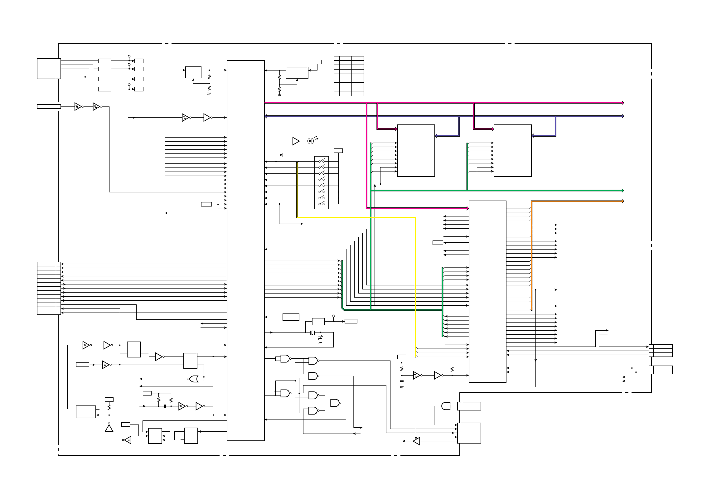
BLOCK DIAGRAM OF MAIN BOARD (1/10)
– 3-3 –
ADR21
ADR20
ADR9
ADR10
ADR11
ADR12
ADR13
ADR14
ADR15
ADR16
ADR17
DATA15
DATA7
DATA14
DATA6
DATA13
DATA5
DATA12
DATA4
ROM0CS
ADR19
ADR18
ADR8
ADR7
ADR6
ADR5
ADR4
ADR3
ADR2
ADR1
DATA0
DATA8
DATA1
DATA9
DATA2
DATA10
DATA3
DATA11
A1
A2
A3
A4
A5
A6
A7
A8
A9
A10
A11
A13
A14
A15
A16
A17
A18
A19
A20
B1
B2
B3
B4
B5
B6
B7
B8
B9
B10
B11
B13
B14
B15
B16
B17
B18
B19
B20
5DAT7
5DAT6
5DAT5
5DAT4
5DAT3
5DAT2
5DAT1
5DAT0
5ADR1
5RD
5WE0
CSGDB
INTGDB
RSTGDB
3
4
5
6
8
9
10
11
13
14
15
16
18
19
CN23
CN401
OPEN
MAIN BOARD (2/10)
ADR21
ADR20
ADR9
ADR10
ADR11
ADR12
ADR13
ADR14
ADR15
ADR16
ADR17
DATA15
DATA7
DATA14
DATA6
DATA13
DATA5
DATA12
DATA4
ROM1CS
ADR19
ADR18
ADR8
ADR7
ADR6
ADR5
ADR4
ADR3
ADR2
ADR1
DATA0
DATA8
DATA1
DATA9
DATA2
DATA10
DATA3
DATA11
A1
A2
A3
A4
A5
A6
A7
A8
A9
A10
A11
A13
A14
A15
A16
A17
A18
A19
A20
B1
B2
B3
B4
B5
B6
B7
B8
B9
B10
B11
B13
B14
B15
B16
B17
B18
B19
B20
CN24
1B1-1B8
DAT8-DAT15
DAT0-DAT7
13,14,16,17
19,20,22,23
2B1-2B8
1A1-1A8
2A1-2A8
1DIR
2DIR
1OE
2OE
1A1
1A2
1A3
1Y1
1Y2
1Y3
2A1
2A2
2A3
2Y1
2Y2
2Y3
4A1
4A2
4A3
4A4
4Y1
4Y2
4Y3
4Y4
1OE
2OE
3OE
4OE
3A4
3Y4
IC38
TRANSCEIVER
IC39
BUFFER
1
24
48
25
2,3,5,6,8,9,11,12
37,38,40,41
43,44,46,47
MDAT8-MDAT15
MDAT (0-15)
MADR (1-21)
ADR (0-25)
DAT (0-31)
CTL (1-26)
PLDRD (1/10)
PLDWE0 (1/10)
DIR (1/10)
MBUF (1/10)
CS (0-30)
MRD,MWE0,MRDWR
MCTL (20-22)
26,27,29,30
32,33,35,36
MDAT0-MDAT7
1A1
1A2
1A3
1A4
1Y1
1Y2
1Y3
1Y4
MADR16
MADR15
MADR14
MADR13
MADR12
MADR11
MADR10
MADR9
MADR8
MADR7
MADR6
MADR5
MADR4
MADR3
MADR2
MADR1
ADR16
ADR15
ADR14
ADR13
ADR12
ADR11
ADR10
ADR9
ADR8
ADR7
ADR6
ADR5
ADR4
ADR3
ADR2
ADR1
2A1
2A2
2A3
2A4
2Y1
2Y2
2Y3
2Y4
4A1
4A2
4A3
4A4
4Y1
4Y2
4Y3
4Y4
1OE
2OE
3OE
4OE
3A1
3A2
3A3
3A4
3Y1
3Y2
3Y3
3Y4
IC40
BUFFER
1A1-1A8
DAT8-DAT15
DAT0-DAT7
13,14,16,17
19,20,22,23
2A1-2A8
1A1
1A2
1A3
1A4
1A5
1A6
1A7
1A8
1B1
1B2
1B3
1B4
1B5
1B6
1B7
1B8
2A1
2A2
2A3
2A4
2A5
2A6
2A7
2A8
A0
SDA
SCL
CLK
#INT
#RESET
#WR
#CS
#RD
2B1
2B2
2B3
2B4
2B5
2B6
2B7
2B8
1DIR
2DIR
1OE
2OE
1B1-1B8
2B1-2B8
1DIR
2DIR
1OE
2OE
IC41
TRANSCEIVER
1A1-1A8
2A1-2A8
1B1-1B8
2B1-2B8
1DIR
2DIR
1OE
2OE
IC43
TRANSCEIVER
IC47
IC42
BUFFER
1
24
48
25
2,3,5,6,8,9,11,12
37,38,40,41
43,44,46,47
5DAT8-5DAT15
26,27,29,30
32,33,35,36
5DAT0-5DAT7
5DIR (1/10)
5BUF (1/10)
5RD (5,6/10)
5WE0 (6/10)
5RDWR (5/10)
UDS (5/10)
LDS (5/10)
WRGP0 (9/10)
SIOCS (6/10)
SICHSL (6/10)
1
48
25
24
2
3
5
8
9
11
19
20
22
23
1
48
25
24
17
47
46
44CTL2
ADR21
ADR20
ADR19
ADR18
ADR17
CTL20
CTL21
CTL22
32
41
40
38
47
46
44
43
41
40
38
37
36
35
33
32
30
29
27
26
30
29
27
26
MRD
MWE0
MRDWR
MCTL20
MCTL21
MCTL22
MADR20
MADR19
MADR18
MADR17
MADR21
2
3
5
6
8
9
11
12
13
14
16
17
19
20
22
23
1
24
48
25
V3D
1
24
48
25
V3D
5ADR1
17
19
20
22
23
5ADR21
5ADR20
5ADR19
5ADR18
5ADR17
13
14
16
2
3
5
6
8
9
11
12
47
46
44
43
41
40
38
37
36
35
33
32
30
29
27
26
CTL2
CS2
CS3
CS16
CS17
CS7
CS30
CTL25
CTL26
ADR21
ADR20
ADR19
ADR18
ADR17
ADR9-ADR16
ADR1-ADR8
37,38,40,41
43,44,46,47
26,27,29,30
32,33,35,36
2,3,5,6
8,9,11,12
13,14,16,17
19,20,22,23
5ADR9-5ADR16
5ADR1-5ADR8
5DAT0-5DAT7
7-9,11-15
18
17
16
5WE0
5CS16
5RD
DB0-DB7
5ADR1
Q39
D42
D43
Q40
6
2
3
1
5
19
5DAT (0-15)
CSGDB (1/10)
3RESET (1/10)
5ADR21
5ADR20
5ADR9
5ADR10
5ADR11
5ADR12
5ADR13
5ADR14
5ADR15
5ADR16
5ADR17
5DAT15
5DAT7
5DAT14
5DAT6
5DAT13
5DAT5
5DAT12
5DAT4
5ADR19
5ADR18
5ADR8
5ADR7
5ADR6
5ADR5
5ADR4
5ADR3
5ADR2
5ADR1
5DAT0
5DAT8
5DAT1
5DAT9
5DAT2
5DAT10
5DAT3
5DAT11
5ADR21
5ADR20
5ADR9
5ADR10
5ADR11
5ADR12
5ADR13
5ADR14
5ADR15
5ADR16
5ADR17
5DAT15
5DAT7
5DAT14
5DAT6
5DAT13
5DAT5
5DAT12
5DAT4
5ADR19
5ADR18
5ADR8
5ADR7
5ADR6
5ADR5
5ADR4
5ADR3
5ADR2
5ADR1
5DAT0
5DAT8
5DAT1
5DAT9
5DAT2
5DAT10
5DAT3
5DAT11
5DAT7
5DAT6
5DAT5
5DAT4
5DAT3
5DAT2
5DAT1
5DAT0
V3D
I2CSDA (7/10)
I2CSCL (7/10)
I2CCLK (4/10)
I2CIRQ (1/10)
5RESET (1/10)
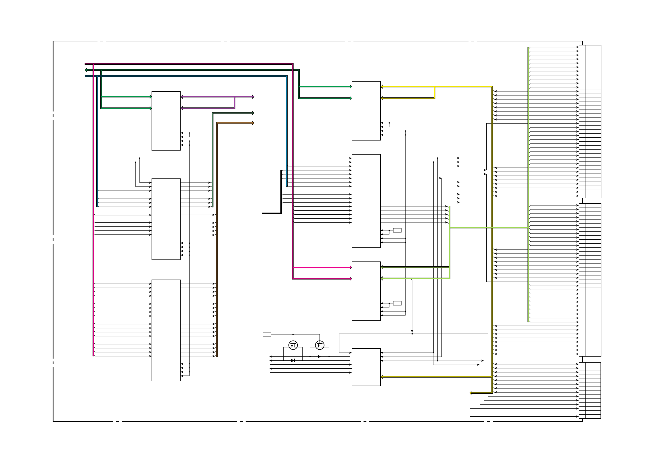
BLOCK DIAGRAM OF MAIN BOARD (2/10)
– 3-4 –
MAIN BOARD (3/10)
Q1
Q2
Q3
Q4
Q5
Q6
Q7
Q8
2
5
6
9
12
15
16
19
D1-D8
#RES
CLK
IC28 D-FF
STRST (4/10)
SRSTA (5/10)
SRSTB (5/10)
SIORST (6/10)
RSFMC0 (9/10)
RSFMC1 (10/10)
MDRST
3DAT8-3DAT15
3,4,7,8
13,14,17,18
1
11
Q1
Q2
Q3
Q4
Q5
Q6
Q7
Q8
2
5
6
9
12
15
16
19
D1-D8
#RES
CLK
IC29 D-FF
1A1-1A8
2A1-2A8
1B1-1B8
2,3,5,6
8,9,11,12
37,38,40,41
43,44,46,47
26,27,29,30
32,33,35,36
2B1-2B8
IC48
TRANSCEIVER
3RESET (1/10)
LEDCS (1/10)
MDAT (0-15)
MADR (1-21)
CS (0-30)
MRD,MWE0,MRDWR
MCTL (20-22)
RSTCS (1/10)
DEC0RS (7/10)
DEC1RS (7/10)
DEC2RS (7/10)
AUDRST (10/10)
FRNRST (1/10)
CNTRST (6/10)
NICRST (4/10)
3DAT0-3DAT7
3,4,7,8
13,14,17,18
1
11
3RESET
Q1
Q2
Q3
Q4
Q5
Q6
Q7
Q8
2
5
6
9
12
15
16
19
4
1
2
5
D1-D8
#RES
CLK
IC26 D-FF
Q29
D39 D38 D37 D36 D35 D34 D33 D32
Q28
Q26
Q24
Q22
3DAT8-3DAT15
3,4,7,8
13,14,17,18
1
11
Q1
Q2
Q3
Q4
Q5
Q6
Q7
Q8
2
5
6
9
12
15
16
19
D1-D8
#RES
CLK
IC27 D-FF
A0-A20 DQ0-DQ15
1-10,16-25,48
#CE
#OE
#WE
#WP
#RP
IC45
FLASH MEMORY
A0-A17 I/O1-I/O16
R/W
#OE
#LB
#UB
#CE
VDD
8
IC46 SRAM
D41
D40
Q38
3DAT0-3DAT7
3,4,7,8
13,14,17,18
1
11
D31 D30 D29 D28 D27 D26 D25 D24
1DIR
2DIR
1OE
2OE
IC50 BUFFER
1Y1
1Y2
1Y3
1Y4
1A1
1A2
1A3
1A4
2A1
2A2
2A3
2A4
3A1
3A2
3A3
3A4
4A1
4A2
4A3
4A4
2Y1
2Y2
2Y3
2Y4
3Y1
3Y2
3Y3
3Y4
4Y1
4Y2
4Y3
4Y4
1OE
2OE
3OE
4OE
37
36
35
33
32
31
30
28
27
26
25
24
23
22
20
19
18
17
16
15
13
12
11
10
9
7
5
MDRST
MDIRQ
EVPLY
MDCS
AWE0
ARD
AADR1
AADR3
AADR2
AADR5
AADR4
AADR7
AADR6
ADAT0
ADAT2
ADAT1
ADAT4
ADAT3
ADAT6
ADAT5
ADAT7
RDGP1
RDGP2
3RESET
RDGP0
CPCS
ECSPLY
CN13
13+
–
CN27
TO
LITHIUM BATTERY
TO
ANALOG
BOARD
. . . . CN13
13+
–
CN28
13,14,16,17
19,20,22,23
MDAT8-MDAT15 3DAT8-3DAT15
3DAT0-3DAT7MDAT0-MDAT7
47
46
44
43
41
40
38
37
MADR12
MADR11
MADR10
MADR9
MADR8
MADR7
MADR6
MADR5
MADR4
MADR3
MADR2
MADR1
36
35
33
32
30
29
27
26
MRD
MWE0
MRDWR
MADR13
1
24
48
25
1
48
25
24
2
3
5
6
8
9
11
12
13
14
16
17
3ADR10
3ADR9
3ADR8
3ADR7
3ADR6
3ADR5
3ADR4
3ADR3
3ADR2
3ADR1
19
20
22
23
DIR (1/10)
CTL23 (1/10)
BUSYI (1/10)
NICRST (4/10)
H2N2 (4/10)
H2N3 (4/10)
H2N4 (4/10)
ECSPLY (10/10)
3BUF (1/10)
3RD (9,10/10)
3WE0 (9,10/10)
3RDWR (6,9,10/10)
3DAT (0-15)
3ADR (1-10)
V3DI (1-10)
MADR1-MADR21
2-5,23-27
29-33,51-54
MADR1-MADR18
1
2
4
IC44
3RESET
CS1
MCTL22
MRD
MCTL21
MCTL20
26
28
11
14
CS0
MRD
MWE0
12
15
42
43
12
13
6,7,10,11,16,
17,20,21,34,
35,38,39,44,
45,48,49
29-36,38-45 MDAT0-MDAT15
3RESET
V5D
V3D
V3D
15
RY/#BY
1A1-1A7
2A1-2A8
1B1-1B7
2B1-2B8
IC51
TRANSCEIVER
1DIR
2DIR
1OE
2OE
3,5,6,8,
9,11,12
38,40,41
43,44,46,47
26,27,29,30
32,33,35,36
13,14,16,17
19,20,22,23
MADR1-MADR7 AADR1-AADR7
ADAT0-ADAT7MDAT0-MDAT7
1
24
48
25
IC53 BUFFER
1Y1
1Y2
1Y3
1A1
1A2
1A3
2
4
6
MRD
MWE0
CS19
CS20
CS21
CS22
11
13
15
17
2A1
2A2
2A3
2A4
2Y1
2Y2
2Y3
2Y4
IC59 BUFFER
Q2
7
D1
D2
D3
D4
CK
#1OE
#2OE
18
16
14
ARD
AWE0
CPCS
RDGP0
RDGP1
RDGP2
MDCS
9
7
5
3
1
19
DIR (1/10)
ABUF (1/10)
MDIRQ (1/10)
EVSPLY (10/10)
4
5
12
13
9
MDAT0
MDAT1
MDAT2
MDAT3
N2H1 (4/10)
N2H3 (4/10)
N2H4 (4/10)
IC60 BUFFER
5
2
9
12
Y1
Y2
Y3
Y4
#OE1
#OE2
#OE3
#OE4
A2
A1
A3
A4
1
4
10
13
3
6
8
11
MDAT0
MDAT1
MDAT2
MDAT3
CS26
CS25
MDAT0-MDAT3MDAT0-MDAT15
CS15
3RESET
RDGP1
RDGP2
RDGP0
CPCS
MDRST
MDCS
AWE0
ARD
CTL23
4
1
2
5
4
1
2
5
4
1
2
5
4
1
2
5
Q25
Q27
Q23
4
1
2
5
4
1
2
5
4
1
2
5
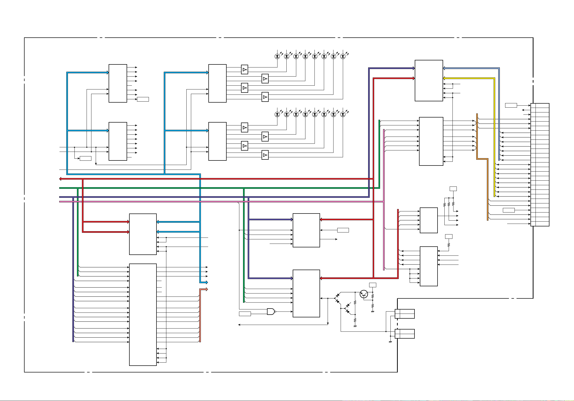
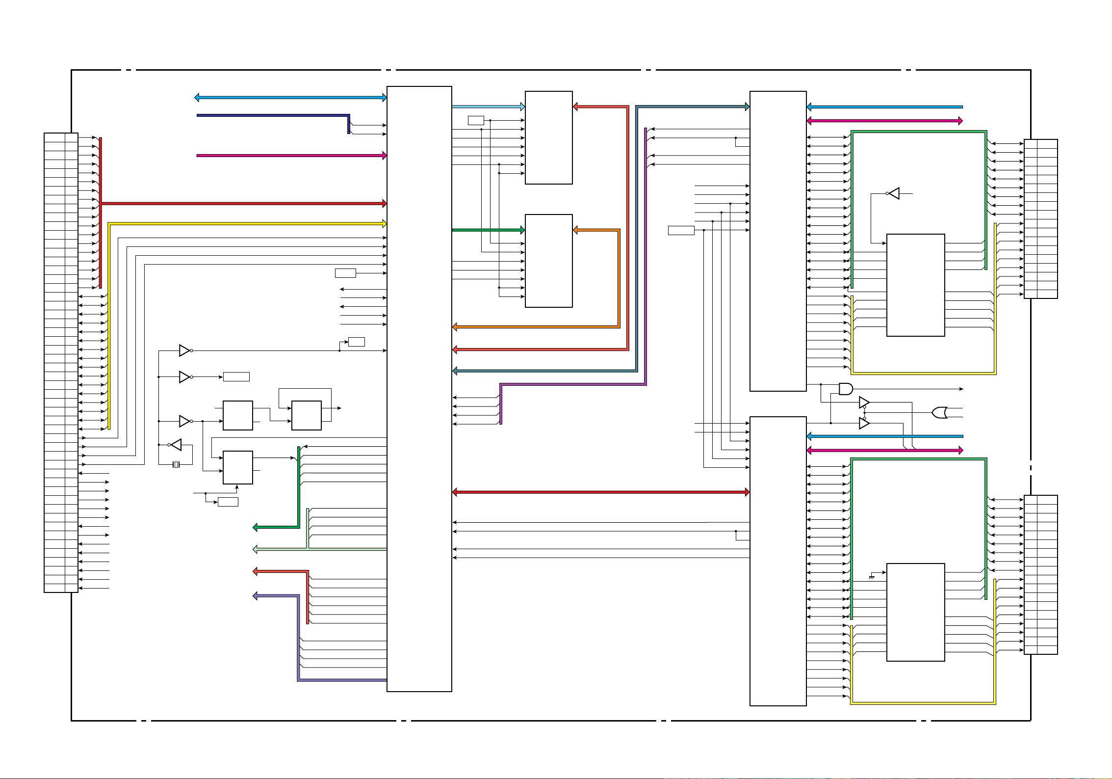
BLOCK DIAGRAM OF MAIN BOARD (3/10)
– 3-5 –
A2
B2
A3
B3
A4
B4
A5
B5
A7
B7
A8
B8
A9
B9
A10
B10
A12
B12
A13
B13
A14
B14
A15
B15
A16
B16
A18
B18
A19
B19
A20
B20
A21
B21
A23
B23
A24
B24
A25
B25
A27
B27
A28
B28
A29
B29
A30
B30
A31
B31
A32
B32
A1
A2
A3
A4
A5
A6
A7
A8
A9
A10
A11
A12
A13
A14
A15
A16
A17
A18
D0
D1
D2
D3
D4
D5
D6
D7
D8
D9
D10
D11
D12
D13
D14
D15
SWAIT
SWE
SRD
SCS
RXD1
TXD1
RA
RB
TA
TB
N2H1
N2H2
N2H3
N2H4
H2N1
H2N2
H2N3
H2N4
CN201
OPEN
IC201 GATE ARRAY
IC203 SDRAM
SPCACS (1/10)
SRSTA (3/10)
5RDWR (2/10)
LDS (2/10)
UDS (2/10)
STCLK
SPCBCS (1/10)
SRSTB (1/10)
CD0-CD15
3-6,292-295
297-302
259-264
269-274
276,277
20-26
29-35
A0-A13 DQ0-DQ15
MAL0-MAL13
MAH0-MAH13
MD16-MD31
MD0-MD15
DA0-DA15
DB0-DB15
61-65,67-72,80-84
88-92,97-109
32-35,43-56A1-A18
7,8,15-18,21-30
D0-D15
CA0-CA17
SCA0-SCA17
SCD0-SCD15
SWAIT
SWE
SRD
SCS
RESET
MCS0
RASL
CASL
MWEL
DQM
CLK
#CS
#RAS
#CAS
#WE
DQML
DQMU
38
19
18
17
16
15
39
288
290
291
289
253
RASH
CASH
MWEH
255
258
254
SDRWA
SDDSA
SDACKA
SDREQA
SDRWB
SDDSB
IREQ
CS
WAIT
FPB
FPA
ASCKB1
VB0-VB7
VA0-VA7
ASCKB2
AALAB1
AARAB2
ASTRBB1
ASTRBB2
129
135
127
130
128
131
ASCKB2
AB1
AB2
ASTBB1
ASTBB2
122
123
124
125
CAENB
CWEB
COEB
CBSYB
149
156
150
157
155
158
AA1
AA2
ASTBA1
ASTBA2
ASCKA1
ASCKA2
144
145
146
147
CAENA
CWEA
COEA
CBSYA
AALAA1
AARAA2
ASTRBA1
ASTRBA2
ASCKA1
ASCKA2
CKI
208,211-217
220-226,231
232-237,240-245
249-252
183-188,193-199
201,202,203
159-162,164-170,173-177 DA0-DA15
DB0-DB15
DMD0-DMD15
MD0-MD15
MD16-MD31
41
RD
WE
MDAT0-MDAT15
MDAT (0-15)
MRD,MWE0,MRDWR
MCTL (20-22)
MADR (1-18)
STIRQ (1/10)
STRCS (1/10)
STWAIT (1/10)
FPIPLY (10/10)
FPIREC (10/10)
IC212(a) D-FF IC212(b) D-FF
I2CCLK (2/10)
STRST (3/10)
TB485 (6/10)
TA485 (6/10)
TXD1 (1/10)
RXD1 (1/10)
RA485 (6/10)
RB485 (6/10)
N2H1 (3/10)
N2HRST (3/10)
N2H3 (3/10)
N2H4 (3/10)
NICRST (3/10)
H2N2 (3/10)
H2N3 (3/10)
H2N4 (3/10)
AB (1,2), ASTBB (1,2)
ASCKB (1,2)
CAENB,CWEB,COEB,CBSYB
JCB (0-7)
CAENA,CWEA,COEA,CBSYA
JCA (0-7)
AA (1,2),ASTBA (1,2)
ASCKA (1,2)
IC827
85
86
MRD
MWE0
MADR1-MADR18
RESET
CLK
36
59
60
31
74
79
87
93
126
148
STCLK
34
b
IC827
12
a
IC827
IC210
X201
56
CLK1
D1
5
#Q1
Q1
2
3
24
c
IC213(a) D-FF
CLK1
#R1
D1
5 ASCKB1
6
#Q1
Q1
2
3
CLK2
D2
9
8
#Q2
Q2
11
6
1
RESET
JCB0-JCB7 110-112,117-121
JCA0-JCA7 136-143
VAENA
VWEA
VOEA
VBSYA
CLK
IC202 SDRAM
20-26
29-35
A0-A13 DQ0-DQ15
CLK
#CS
#RAS
#CAS
#WE
DQML
DQMU
IC301
SCSI-3 PROTOCOL CONTROLLER
IC341 TERMINATOR
Q341
DMD0-DMD15
51,52,55,56
19,20,22-24,26-29,32-34,36-39
51,52,55,56
19,20,22-24,26-29,32-34,36-39
#CS0
#RESET
R/#W
#LDS
#UDS
SCLK
DMR/#W
#DMLDS
#DMUDS
#DACK
DREQ
101
90
103
104
105
106
74
75
76
78
91
92
94
95
96
97
99
100
89
87
86
85
84
83
81
80
79
STANDBY
SGLINE14
SGLINE13
SGLINE12
SGLINE11
SGLINE15
SGLINE16
SGLINE17
SGLINE18
SCNTA3
SCNTA2
38
19
18
17
16
15
39
2,4,5,7,8,10,11,13
42,44,45,47,48
50,51,53
1,3-5,7,9-11,13,14
138,139,141-144
1,3-5,7,9-11,13,14
138,139,141-144
2,4,5,7,8,10,11,13
42,44,45,47,48
50,51,53
MD0-MD15
DA0-DA15
MD16-MD31
178
179
180
182
SCNTA3
SCNTA2
SCNTA1
SCNTA0
SCNTB3
SCNTB2
204
205
26
27
28
29
30
31
32
33
34
41
43
44
45
46
47
48
49
50
DBA0
DBA1
DBA2
DBA3
DBA4
DBA5
DBA6
DBA7
LDBP
SCA8
SCA7
SCA6
SCA5
SCA4
SCA3
SCA2
SCA1
SCA0
CN301
26
27
28
29
30
31
32
33
34
41
43
44
45
46
47
48
49
50
DBB0
DBB1
DBB2
DBB3
DBB4
DBB5
DBB6
DBB7
LDBP
SCB8
SCB7
SCB6
SCB5
SCB4
SCB3
SCB2
SCB1
SCB0
CN351
135
133
132
129
130
48
127
46
44
42
54
A1-A4
A1-A4
D0-D15
#UDBP
#LDBP
#DB15
#DB14
#DB13
#DB12
#DB11
#DB10
#DB9
#DB8
#DB7
#DB6
#DB5
#DB4
#DB3
#DB2
#DB1
#DB0
#ATN
#BSY
#ACK
#RST
#MSG
#SEL
#C/D
#REQ
#I/O
SCNTA1
SCNTA0
48
127
46
44
42
54
#INT
IC351
SCSI-3 PROTOCOL
CONTROLLER
IC393
IC392
IC392
IC391
#CS0
#RESET
R/#W
#LDS
#UDS
SCLK
#INT
D0-D15
#UDBP
#LDBP
#DB15
#DB14
#DB13
#DB12
#DB11
#DB10
#DB9
#DB8
#DB7
#DB6
#DB5
#DB4
#DB3
#DB2
#DB1
#DB0
#ATN
#BSY
#ACK
#RST
#MSG
#SEL
#C/D
#REQ
#I/O
DMR/#W
#DMLDS
#DMUDS
#DACK
DREQ
135
133
132
129
130
SGLINE1
SGLINE2
SGLINE3
SGLINE4
SGLINE5
5ADR1-5ADR4
5DAT0-5DAT15
5ADR1-5ADR4
5DAT0-5DAT15
5DAT (0-15)
5DAT (0-15)
5ADR (1-21)
SPCIRQ (1/10)
TO
SCSI-IDE
BOARD
. . . . CN3
TO
EXTENSION
STORAGE
PORT
TO
COPY PORT
SIRQCS (1/10)
5RD (2/10)
TERM (6/10)
5ADR (1-21)
101
90
103
104
105
106
74
75
76
78
91
92
94
95
96
97
99
100
89
87
86
85
84
83
81
80
79
SGLINE10
SGLINE9
SGLINE8
SGLINE7
SGLINE6
DBA17
DBA16
DBA15
DBA14
DBA13
DBA12
DBA11
DBA10
DBA9
DBA8
DBA7
DBA6
DBA5
DBA4
DBA3
DBA2
DBA1
DBA0
DBB17
DBB16
DBB15
DBB14
DBB13
DBB12
DBB11
DBB10
DBB9
DBB8
DBB7
DBB6
DBB5
DBB4
DBB3
DBB2
DBB1
DBB0
SCA8
SCA7
SCA6
SCA5
SCA4
SCA3
SCA2
SCA1
SCA0
SCB8
SCB7
SCB6
SCB5
SCB4
SCB3
SCB2
SCB1
SCB0
1
5
7
8
9
10
11
SCA8
SCA7
SCA6
SCA5
SCA8
SCA7
SCA6
SCA5
SCA4
SCA3
SCA2
SCA1
SCA0
SCB8
SCB7
SCB6
SCB5
SCB4
SCB3
SCB2
SCB1
SCB0
2
3
4
23
22
21
20
DBA5
DBA6
DBA7
DBA16
18
17
16
15
14
SCA0
SCA1
SCA2
SCA3
SCA4
IC394 TERMINATOR
STANDBY
SGLINE14
SGLINE13
SGLINE12
SGLINE11
SGLINE15
SGLINE16
SGLINE17
SGLINE18
SGLINE1
SGLINE2
SGLINE3
SGLINE4
SGLINE5
SGLINE10
SGLINE9
SGLINE8
SGLINE7
SGLINE6
1
5
7
8
9
10
11
SCB8
SCB7
SCB6
SCB5
2
3
4
23
22
21
20
DBB5
DBB6
DBB7
DBB16
18
17
16
15
14
SCB0
SCB1
SCB2
SCB3
SCB4
DBA0
DBA1
DBA2
DBA3
DBA4
DBA5
DBA6
DBA7
DBA16
DBB0
DBB1
DBB2
DBB3
DBB4
DBB5
DBB6
DBB7
DBB16
50
50
4
1
62
1
1
2
4
7
35
2
a
b
MAIN BOARD (4/10)/(5/10)
5DAT0
5DAT1
VAENB
VWEB
VOEB
VBSYB
SCNTB1
SCNTB0
206
207
SDACKB
SDREQB
BLOCK DIAGRAM OF MAIN BOARD (4/10)/(5/10)

– 3-6 –
5DAT(0-15)
3DAT(0-15)
5ADR(1-21)
5RD (2/10)
3RDWR (3/10)
REARW0 (1/10)
REARW1 (1/10)
REARR0 (1/10)
REARR1 (1/10)
ETCRCS (1/10)
TA485,TB485,RA485,RB485 (4/10)
UPSIRQ (1/10)
3DAT3 (3/10,9/10,10/10)
NMI (1/10)
CTXD (1/10)
CRXD (1/10)
CNTRST (3/10)
5WE0 (2/10)
SIORST (3/10)
SIOCS (2/10)
485IRQ (1/10)
232IRQ (1/10)
SICHSL (2/10)
2-4,43-47
26-28
5DAT(0-7)
CONNECT
UPS
NMI
CTXD
CRXD
CNTRST
TERM
3DAT(0-7)
3ADR1
D0-D7
19
#RD1
16
#WR1
35
MR
11
#CS2
10
2
CS1
30
INTRPT
30
INTRPT
4
2
4
7
1
5
3
A0-A2
5ADR(1-3)
5DAT(0-7)
5ADR(1-3)
2-4,43-47
26-28
D0-D7
19
#RD1
16
#WR1
35
8
33
32
40
7
39
38
41
MR
11
#CS2
10
CS1
SOUT
#DTR
#RTS
#DCD
#DSR
#CTS
38
#CTS
#RI
SIN
5
7
11
6
8
9
10
12
DR1OUT
TXD
DTR
RTS
DCD
RXD
DSR
CTS
RI
TXD
CTXD
UPS
TERM
NMI
CRXD
CNTRST
CONNECT
DTR
RTS
DCD
RXD
DSR
CTS
RI
TXD
TXD
DTR
DTR
RTS
RTS
DCD
DCD
RXD
RXD
DSR
DSR
CTS
CTS
RI
RI
DR2OUT
DR3OUT
RX1IN
RX3IN
RX4IN
RX5IN
RX2IN
A0-A2
15
XOUT
14
XIN
14
XIN
12
#BAUDOUT
5
RCLK
33
#DTR
39
#DSR
12
#BAUDOUT
5
RCLK
IC431
S/P, P/S CONVERTER
IC430
S/P, P/S CONVERTER
25
DR1IN
23
DR2IN
19
DR3IN
24
RX1OUT
22
RX2OUT
21
RX3OUT
20
RX4OUT
18
RX5OUT
6
7
1
2
Q1
#Q1
5
4
B1
IC416
RS-232C I/F
IC429
IC419(a)
MONOSTABLE
MULTIVIBRATOR
8
SOUT
7
SIN
1
2
6
3
4
5
a
IC401
11
B2
10
Q2
IC419(b)
MONOSTABLE
MULTIVIBRATOR
9
Y
11
B
2
R
5
D
4
DE
IC418
RS485 DRIVER
2
5
4
6
8
3
10
9
2
1
A1
3
A2
4
A3
5
A4
6
A5
7
A6
8
A7
9
6
1
7
A8
1
DIR
19
2
5
3
G
11-18
B1-B8
IC425
TRANSCEIVER
13
10
6
3
14
11
5
2
4B
3B
2B
1B
4A
3A
2A
1A
12
4Y
9
3Y
7
2Y
4
15
1Y
OC
1
S
IC301
Q106
Q116
Q126
Q101
Q156
Q166
Q176
Q186
CN402 CN402
IC426
IC426
IC426
IC427
TERM (5/10)
11
B
12
13
11
1
8
d
b
IC401
IC401
IC401
8
9
10
c
12
A
2
R
RA485
TA485
TB485
RA485
RB485
RB485
TB485
TA485
IC417
RS485 RECEIVER
IC412
IC432
IC414
IC414
a
c
8
9
10
11
12
13
14
15
16
17
18
19
20
21
22
24
25
27
28
29
30
32
33
34
35
39
40
41
42
43
44
45
46
RDAT7
RDAT6
RDAT5
RDAT4
RDAT3
RDAT2
RDAT1
RDAT0
GND
RADR1
REARW0
REARW1
REARR0
REARR1
UPS
TERM
NMI
TA
TB
RA
RB
CTXD
CRXD
CNTRST
CCONNECT
DCD
DSR
RXD
RTS
TXD
CTS
DTR
RI
7
10
9
12
11
14
13
16
15
18
17
20
19
22
21
23
26
28
27
30
29
31
34
33
36
40
39
42
41
44
43
46
45
RDAT7
RDAT6
RDAT5
RDAT4
RDAT3
RDAT2
RDAT1
RDAT0
GND
RADR1
REARW0
REARW1
REARR0
REARR1
UPS
TERM
NMI
TA
TB
RA
RB
CTXD
CRXD
CNTRST
CCONNECT
DCD
DSR
RXD
RTS
TXD
CTS
DTR
RI
CN304
1
2
3
4
6
7
8
9
DCD
RXD
TXD
DTR
DSR
RTS
CTS
RI
a
c
b
a
b
IC427
CN302
1
2
3
4
TXD
RXD
CONNECT
RST
CN12
CN305
CN303
TO
MAIN
BOARD
. . CN12
9
7
5
3
1
AREC
APLY
ASEL
SUBSPTOUT
PLYOUT
CN301
IN
OUT
AUDIO
REMOTE
(WV-CU50)
DATA
SERIAL
MULTISCREEN OUT
SPOT OUT
2
3
4
5
RX(B)
RX(A)
TX(B)
TX(A)
CTXD
CRXD
CNTRST
CONNECT
CNTRST
CRXD
CONNECT
CTXD
TA
TB
RA
RB
RB
RA
TB
TA
SW302
27364
5
TERM
TERM
3ADR1
REARW0
REARW1
REARR0
REARR1
BD7
BD6
BD5
BD4
BD3
BD2
BD1
BD0
BD7
BD6
BD5
BD4
REARR1
3ADR1
AL16
AL15
AL14
AL13
AL8
AL7
AL6
AL5
AL16
AL15
AL14
AL13
AL8
AL7
AL6
AL5
13
10
6
3
14
11
5
2
4B
3B
2B
1B
4A
3A
2A
1A
12
4Y
9
3Y
7
2Y
4
15
1Y
OC
1
S
IC302
Q111
Q121
Q131
Q146
Q171
Q181
Q191
Q196
BD3
BD2
BD1
BD0
REARR1
3ADR1
AL12
AL11
AL10
AL9
AL4
AL3
AL2
AL1
AL12
AL11
AL10
AL9
AL4
AL3
AL2
AL1
13
10
6
3
14
11
5
2
4B
3B
2B
1B
4A
3A
2A
1A
12
4Y
9
3Y
7
2Y
4
15
1Y
OC
1
S
IC303
Q201
Q206
Q216
Q276
Q241
Q221
Q211
BD7
BD6
BD5
BD4
REARR0
3ADR1
OP21
OP16
OP15
PDET
EMI
TSUM
TAJI
OP21
OP16
OP15
PDET
EMI
TSUM
TAJI
13
10
6
3
14
11
5
2
4B
3B
2B
1B
4A
3A
2A
1A
12
4Y
9
3Y
7
2Y
4
15
1Y
OC
1
S
IC304
Q226
Q236
Q246
Q251
Q301
Q136
Q161
BD3
BD2
BD1
BD0
REARR0
3ADR1
OP14
OP13
OP12
OP11
OP14
OP13
OP12
OP11
SEL2
SEL1
15
12
10
7
5
2
4B
3B
2B
1B
4A
3A
14
4Y
13
3Y
11
2Y
6
4
1Y
1Y
3
9
OC
CK
IC305
IC306
Q151
Q252
Q231
Q296
Q266
BD5
BD4
BD3
BD2
BD1
BD0
REARW1
REOUT
ALOUT
TAJO
POUT
PST
EMO
REOUT
ALOUT
SEL2
SEL1
15
12
10
7
5
2
6
5
1
8
8
7
14
1
6
1
2
4B
3B
2B
1B
4A
3A
1
13
2
5
5
8
5
14
4Y
13
3Y
11
2Y
6
4
1Y
1Y
3
9
OC
CK
Q261
Q286
Q281
Q298
TP301
Q291
IC309(d)
Q302
IC308(d) IC308(a)
IC308(b),(c)
IC310
VR301
VR302
BD5
BD4
BD3
BD2
BD1
BD0
REARW0
HDD
DVD
REC4
REC3
REC2
REC1
TAJO
POUT
PST
EMO
HDD
DVD
REC4
REC3
REC2
REC1
Q271
Q141
CN101 ALARM PORTCN201 CONTROL PORT
AMP
IC309(b),(c)
IC309(a)
IC307
IC311
AMP
AMP
AMP
BIAS
MUTE
AMPAMP
BUFFER
REAR BOARDMAIN BOARD (6/10)
BLOCK DIAGRAM OF MAIN BOARD (6/10) / REAR BOARD
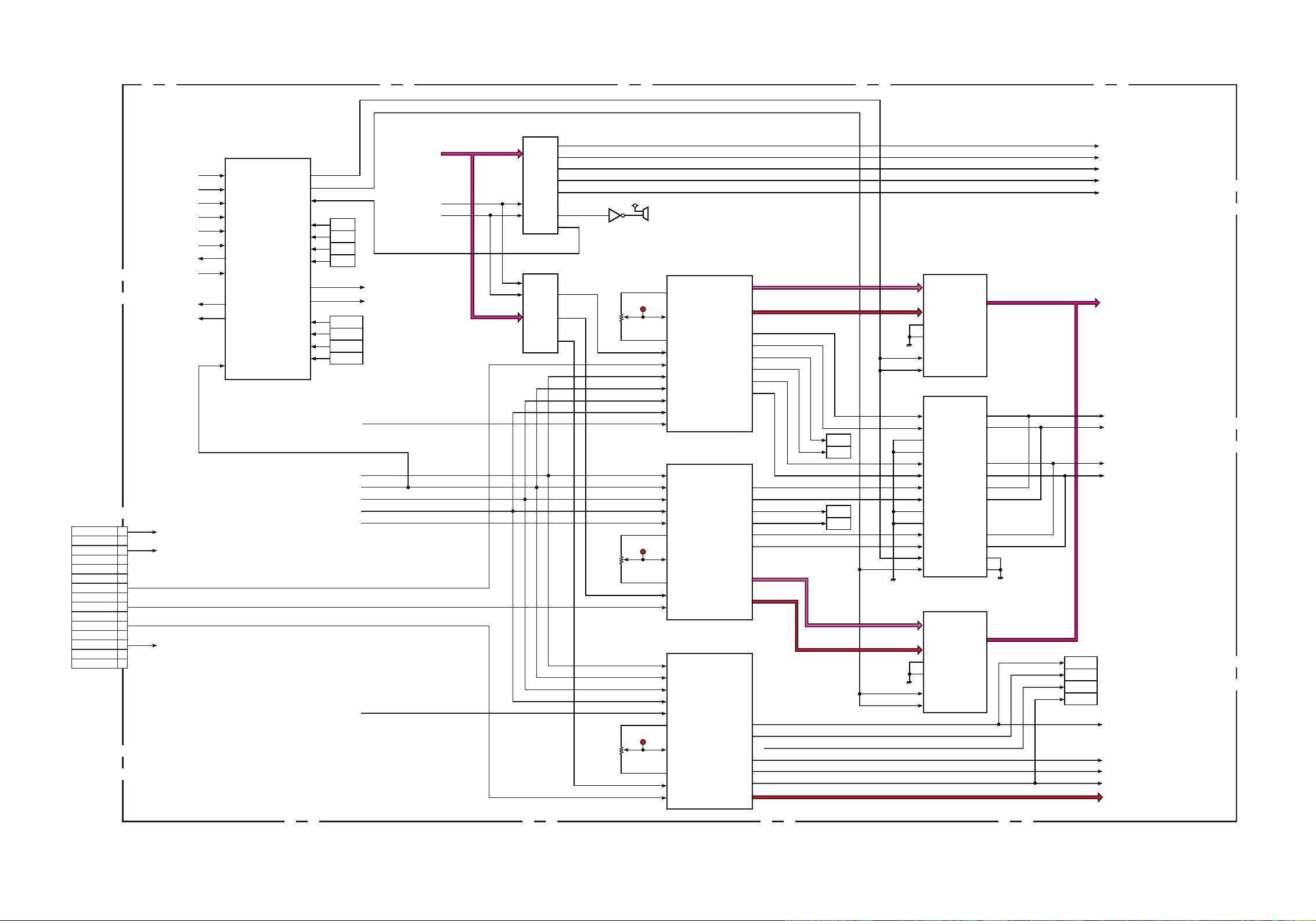
– 3-7 –
D1-D8
Q1
Q2
Q5
Q6
Q8
Q4
Q7
Q1
Q2
Q3
D1-D8
CLK
#RES
IC815
LATCH
V5D
Q801
BZ801
IC814
LATCH
IC601
A/D CONVERTER
IC551
A/D CONVERTER
CLK
#RES
2
5
12
15
19
9
16
2
5
6
23
VIN1
23
VIN1
89
M[2]
89
M[2]
17
VRCL1
13
VRB1
24
VRT1
TP602
VR601
89
M[2]
23
VIN1
80
CLKX2
28
MODE[1]
39
SCL
40
SDA
36
RESET-L
3,4,7,8,13,
14,17,18
5RESET (1/10)
PLYSEL (10/10)
DCKPLY (10/10)
DVVPLY (10/10)
DHVPLY (10/10)
DOEPLY (10/10)
DY(0-7) PLY,DC(0-7) PLY (10/10)
DY(0-7) REC,DC(0-7) REC (9/10)
MDSEL (10/10)
ASEL (10/10)
SPTMSK (10/10)
STPCNT (10/10)
5DAT (0-15)
5DAT(0-7)
5DAT(8-15)
WRGP0 (2/10)
DEC27M (9/10)
PALnNT (1/10)
I2CSCL (2/10)
I2CSDA (2/10)
DEC0RS (3/10)
DEC1RS (3/10)
DEC2RS (3/10)
CPOUT0 (8/10)
MDVA (8/10,10/10)
TO
ANALOG
BOARD
. . . CN11
3,4,7,8,13,
14,17,18
1
11
1
11
15
14
13
12
11
10
9
8
7
6
5
4
3
2
1
CPOUT0
AGND
CPOUT1
AGND
CPOUT2
AGND
REC1V
AGND
REC2V
AGND
MULTV
AGND
MDVA
AGND
AGND
CN11
IC651
A/D CONVERTER
80
CLKX2
28
MODE[1]
39
SCL
40
SDA
36
RESET-L
80
CLKX2
28
MODE[1]
39
SCL
40
SDA
36
RESET-L
17
VRCL1
13
VRB1
Y[0]-Y[7]
53-60
C[0]-C[7]
CLKXO
63-70
76
HSYNC-L
75
VSYNC-L
74
VVALID
73
HVALID
72
ODD/EVEN
71
CLKXO
76
HSYNC-L
75
VSYNC-L
74
VVALID
73
HVALID
72
ODD/EVEN
71
CLKXO
76
HSYNC-L
75
VSYNC-L
74
VVALID
73
HVALID
72
ODD/EVEN
71
Y[0]-Y[7]
53-60
Y[0]-Y[7]
C[0]-C[7]
53-60,63-70
C[0]-C[7]
63-70
24
VRT1
TP601
VR551
17
VRCL1
13
VRB1
24
VRT1
TP603
VR651
CPOUT1 (8/10)
IC552
BUFFER
2,3,5,6,
8,9,11,12
1
24
13,14,16,17,
19,20,22,23
2B1-2B8
1B1-1B8
1DIR
2DIR
1A1-1A8
2A1-2A8
26,27,29,30,32,
33,35-38,40,41,
43,44,46,47
25
#2OE
48
#1OE
2
3
5
6
8
9
13
14
16
17
19
20
IC691
BUFFER
1B1
1B2
1B3
1B4
1B5
1B6
2B1
2B2
2B3
2B4
2B5
2B6
1A1
1A2
1A5
1A6
2A1
2A2
2A5
2A6
47
46
41
40
36
35
30
29
48
#1OE
25
#2OE
1
24
1DIR
2DIR
IC602
BUFFER
2,3,5,6,
8,9,11,12
1
24
13,14,16,17,
19,20,22,23
2B1-2B8
1B1-1B8
1DIR
2DIR
1A1-1A8
2A1-2A8
26,27,29,30,32,
33,35-38,40,41,
43,44,46,47
25
#2OE
48
#1OE
MAIN BOARD (7/10)
DCKREC (9/10)
DHSREC (9/10)
DHVREC (9/10)
DOEREC (9/10)
IC828
PLD
1
40
PTD0
FPINT
FPVIDEO
CLK27M
TCK
TMS
TDO
TDI
DECSEL1
DECSEL2
DECSEL
V1
VVALID1
V2
VVALID2
3
5
8
28
32
4
NTPAL-P
10
#PTD0 (1/10)
FPIREC (9/10)
FPVREC (9/10)
E27REC (9/10)
PLDTCK (1/10)
DVSREC (9/10)
DVVREC (9/10)
PLDTMS (1/10)
PLDTDO (1/10)
HOUT-P
VOUT-P
14
DHSPLY (10/10)
16
DVSPLY (10/10)
PLDTDI (1/10)
35
33
47
20
21
23
24
27
26
H-P
V-P
CLK-P
ODD-P
9
12
29
11
PLDVIN
DOEPLY
DCKPLY
PLDHIN
D1VS
D1VV
D2VS
D2VV
DCKPLY
DOEPLY
PLDHIN
PLDVIN
D2VS
D2VV
D1VS
D1VV
VOUT
VVALID
BLOCK DIAGRAM OF MAIN BOARD (7/10)
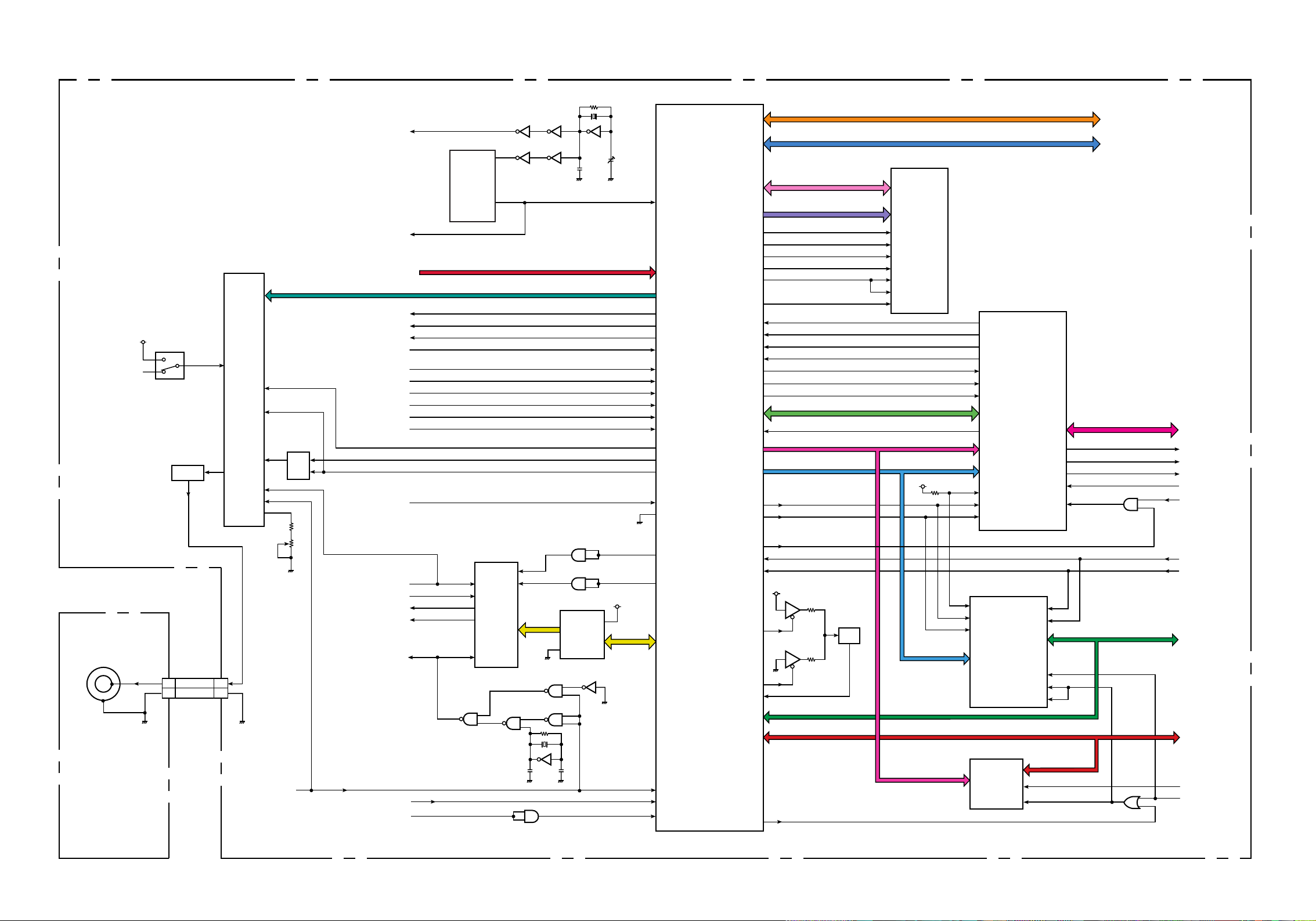
– 3-8 –
IC801
FRAME MEMORY CONTROL
IC803
JPEG ENCODER
IC802
FRAME MEMORY
IC804
TRANSCEIVER
IC818,Q802,
D801,CT802
IC805
IC808
IC819
IC822
1
3RDWR (3/10)
JD0REC-JD7REC
JD0REC-JD7REC
3DAT0-3DAT7
CSJPG0 (1/10)
3RD (3/10)
CBSYA (4/10)
INTJ0 (1/10)
COEA (4/10)
CWEA (4/10)
CAENA (4/10)
3WE0 (3/10)
3ADR(1-10)
3DAT(0-15)
JCA(0-7)
AA(1,2),ASTBA(1,2),ASCKA(1,2)
PCM (REC,SCK,LR,MCK)
2
11-18
1
A1-A8
B1-B8
48
25
#1OE
#2OE
30
35-38,40,41,
43,44,46,47
3ADR1-3ADR10
2A5
103-107
HA0-HA4
108
109
HRD
113
JPASS1
129
JWR
128
JCS
HWR
164
APLLV(UP)
2
5
163
6
3
1
7
a
b
APLLREF(DOWN)
165
AMCLK IN
151
157
155
JDCLK
JCLKEN
152
158
JDSYNC
JRESET
153
154
JSTOP
156
JCOMP
JEND
GEOS
190
189
FMWE
FMCAS
127
JACC
1A1-1A8,2A1,2A2
JA0REC-JA9REC
JA0REC-JA9REC
3ADR1-3ADR5
83-88,90-92,
94-99,102
HD0-HD15
3DAT0-3DAT15
VCO
DIR
G
19
4
2-9
IC806
TRANSCEIVER
IC810
IC811
IC811
IC811
IC811
VR701
IC756(b)
D-FF
IC701
D/A
CONVERTER
Q701,Q706
IC810
IC809
IC820
2-9
1
9
10
B1-B8
G
A1-A8
DIR
11-18
QCKD
5
19
11
IC807
OSD CONTROL
32
1-8
2
3
2
1
13
a
b
d
c
7
1
12
6
3
1
2
10
CN700
CN1
E1
9
8
4
4
5
AC
AD0-AD7
CS
31
SCK
9
VOUT
27
2-8,10-14,
17-20
VSY
51
VCLK
BUFFER
28
HSY
GD0-GD7
BD0-BD7
39
HOR
16
P2
26
P1
25
OSCIN
22
8
132-138,141
JDATA0-JDATA7
142-148,150
JPIXEL4-JPIXEL11
DQ0-DQ15
2,4,5,7,8,10,11,13,42,
44,45,47,48,50,51,53
A0-A13
#WE
#CAS
20-26,29-35
16
17
188
187
FMRAS
FMCS
#RAS
#CS
18
19
178
FMDQM
DQML
DQMU
15
185
FMCLK
CLK
38
39
209,212-219,
222-228
172-177
166-169
FMDQ0-FMDQ15
SAD1,SAD2,SSTRB1,
SSTRB2,SSCLK1,SSCLK2
AMCLK,ALRCLK
ASCLK,ASDIN
193-199,202-208
FMA0-FMA13
DATA0-DATA7
82-89
#END
V3D
12
CLKEN
61
DCLK
60
#RESET
56
#DSYNC
37
#EOS
34
#STOP
33
COMP
30
PIXEL4-PIXEL11
38-43,46,47
97
96
95
DC0-DC7,DY0-DY7
CLK54 IN
1
3,4,6,8-19,22
183
X1/CLK
5
CLK
EC0-EC7,EY0-EY7
DC(0-7) REC,DY(0-7) REC
EC(0-7) REC,EY(0-7) REC
FPVREC (1,7/10)
54MQ1 (10/10)
DEC27M (7/10)
FPIREC (1,4,7/10)
29-32,34-39,42-47
FPVIDEO (SOT)
7
FPINT
58
INTFC0 (1/10)
CSFMC0 (1/10)
HINT
110
OSDSW
15
52
RSTB
22
NTB
42
IR
EV
53
EH
54
5RESET (1/10)
OHOR1 (10/10)
WHITE1 (10/10)
CHAR1 (10/10)
ECLK27
55
EODDPL (10/10)
EXTODDIN
63
OSDCS
78
OSDOSC (10/10)
PALnNT (1/10)
OBLNK1 (10/10)
OSDSCK
79
AMODE
162
OSDD0-OSDD7
68-71,
74-77
OSDBLANK
82
NTSCPAL (TIN)
232
HCS
111
DOEREC (7/10)
DODD
23
DCKREC (7/10)
DCLK
24
DHSREC (7/10)
DHSYNC
25
DVSREC (7/10)
DVSYNC
26
DVVREC (7/10)
DVVALID
27
DHVREC (7/10)
DHVALID
28
ADDR0-ADDR9
1-10
1B1-1B7,2B1,2B2
2,3,5,6,
8,9,11-14
16
17
19
114-119,123-126
JADDR0-JADDR9
32
1
2
33
2A4
2A3
68
#CBUSY
4
99
#INT
64
#CAEN
67
#COE
66
#CWE
71-76,78,79
CODE0-CODE7
c
12
13
11
d
V5D
V3A
RSFMC0 (3/10)
SYSRESET
231
2
6
a
b
IC817
IC824
CT801
2
6
b
IC817
5
3
c
IC823
5
3
c
7
1
a
IC817
7
1
a
#RD
#WR
#CS
2B3
2B4
2B5
MAIN BOARD (8/10)/(9/10)
BNC BOARD
GENLOCK
GND
1
2
1
2
2,3
1
4
SW11
V5
BLOCK DIAGRAM OF MAIN BOARD (8/10)/(9/10) / BNC BOARD
 Loading...