

Panasonic WJ-FS109, WJ-FS116 Service Manual
SPECIFICATIONS
Power Source : 220 – 240 V AC 50 Hz
Power Consumption : 12 W
Camera Input (1-16)/(1-9)
∗: 1.0 V[p-p] /75 Ω 2:1 interlaced composite video signal
Playback Input : 1.0 V[p-p] /75 Ω composite video signal
Camera Switching Input : 1 RCA pin jack
Sampling Frequency : 4 fsc 17 MHz
Quantizing : 8 bit
Pixels : 720 x 544
Maximum Refreshing Rate : 4 fields/second
Camera Output (1-16)/(1-9)
∗: Looped through Camera Input, 75 Ω automatic termination
Recording Output : 1.0 V[p-p] composite video signal, Multiplexed with Camera ID
Monitor Output : 1.0 V[p-p] /75 Ω composite video signal
Buzzer : 1 Built in
Alarm/Remote Control : 25-pin D-sub Connector
Ambient Operating Temperature : –10°C - +50°C (14°F - 122°F)
Ambient Operating Humidity : Less than 90 %
Dimensions : 420 (W) x 44 (H) x 350 (D) mm [16-9/16” (W) x 1-3/4” (H) x 13-3/4” (D)]
Weight : 4 kg (8.8 lbs.)
Dimensions and weight are approximate.
Specifications are subject to change without notice.
Specifications marked with
∗apply to WJ-FS109.
STANDARD ACCESSORIES
Rack Mounting Bracket . . . . . . . . . . . . . . . . . . . . . . . . . 2 pcs.
Screws (M3 x 10) . . . . . . . . . . . . . . . . . . . . . . . . . . . . . 6 pcs.
Switch Protector . . . . . . . . . . . . . . . . . . . . . . . . . . . . . . 1 pc.
WJ-FS109/WJ-FS116
ORDER NO. AVS9911xxxC8
O
N
P
O
W
E
R
O
F
F
Video Multiplexer WJ-FS
109
FS
C 1999 Matsushita Communication Industrial Co., Ltd.
All rights reserved. Unauthorized copying and
distribution is a violation of law.
Video Multiplexer
This service information is designed for experienced repair technicians only and is not designed for use by the
general public.
It does not contain warnings or cautions to advise non-technical individuals of potential dangers in attempting to
service a product.
Products powered by electricity should be serviced or repaired only by experienced professional technicians. Any
attempt to service or repair the product or products dealt with in this service information by anyone else could
result in serious injury or death.
Y
WARNING
CAUTION
RISK OF ELECTRIC SHOCK
DO NOT OPEN
CAUTION:
TO REDUCE THE RISK OF ELECTRIC SHOCK,
DO NOT REMOVE COVER (OR BACK). NO USER
SERVICEABLE PARTS INSIDE.
REFER SERVICING TO QUALIFIED SERVICE
PERSONNEL.
This symbol warns the user that uninsulated voltage within
the unit may have sufficient magnitude to cause electric
shock. Therefore, it is dangerous to make any kind of contact
with any inside part of this unit.
This symbol alerts the user that important literature concerning
the operation and maintenance of this has been included.
Therefore, it should be read carefully in order to avoid
any problems.
There are special components used in this equipment which are important for safety. These parts are indicated
by the ” Y ” mark on the schematic diagram and the replacement parts list. It is essential that these critical
parts should be replaced with manufacturer's specified parts to prevent X-radiation, shock, fire, or other hazards.
Do not modify the original design without permission of manufacture.
IMPORTANT SAFETY NOTICE
CONTENTS
Major Operating Controls and Their Functions . . . . . . . . . . . . . . . . . . . . . . . . . . . . . . . . . . . . . . . . . . . . . . . . . . . . . . . . . . . . . . 1
Adjustment Procedure . . . . . . . . . . . . . . . . . . . . . . . . . . . . . . . . . . . . . . . . . . . . . . . . . . . . . . . . . . . . . . . . . . . . . . . . . . . . . . . . . . 4
Location of Test Points and Adjusting Controls . . . . . . . . . . . . . . . . . . . . . . . . . . . . . . . . . . . . . . . . . . . . . . . . . . . . . . . . . . . . . 6
WIRING Diagram . . . . . . . . . . . . . . . . . . . . . . . . . . . . . . . . . . . . . . . . . . . . . . . . . . . . . . . . . . . . . . . . . . . . . . . . . . . . . . . . . . . . . . . 7
Block Diagram
WJ-FS109 . . . . . . . . . . . . . . . . . . . . . . . . . . . . . . . . . . . . . . . . . . . . . . . . . . . . . . . . . . . . . . . . . . . . . . . . . . . . . . . . . . . . . . . . . . . 8
WJ-FS116 . . . . . . . . . . . . . . . . . . . . . . . . . . . . . . . . . . . . . . . . . . . . . . . . . . . . . . . . . . . . . . . . . . . . . . . . . . . . . . . . . . . . . . . . . . . 9
Schematic Diagram
Main Board (1/2)/D Sub Board . . . . . . . . . . . . . . . . . . . . . . . . . . . . . . . . . . . . . . . . . . . . . . . . . . . . . . . . . . . . . . . . . . . . . . . . . . . 10
Main Board (2/2)/BNC Board . . . . . . . . . . . . . . . . . . . . . . . . . . . . . . . . . . . . . . . . . . . . . . . . . . . . . . . . . . . . . . . . . . . . . . . . . . . . . 11
Front Board . . . . . . . . . . . . . . . . . . . . . . . . . . . . . . . . . . . . . . . . . . . . . . . . . . . . . . . . . . . . . . . . . . . . . . . . . . . . . . . . . . . . . . . . . . 13
Power Board . . . . . . . . . . . . . . . . . . . . . . . . . . . . . . . . . . . . . . . . . . . . . . . . . . . . . . . . . . . . . . . . . . . . . . . . . . . . . . . . . . . . . . . . . 14
Conductor View
Main Board/D Sub Board/BNC Board . . . . . . . . . . . . . . . . . . . . . . . . . . . . . . . . . . . . . . . . . . . . . . . . . . . . . . . . . . . . . . . . . . . . . . 12
Front Board . . . . . . . . . . . . . . . . . . . . . . . . . . . . . . . . . . . . . . . . . . . . . . . . . . . . . . . . . . . . . . . . . . . . . . . . . . . . . . . . . . . . . . . . . . 13
Power Board . . . . . . . . . . . . . . . . . . . . . . . . . . . . . . . . . . . . . . . . . . . . . . . . . . . . . . . . . . . . . . . . . . . . . . . . . . . . . . . . . . . . . . . . . 15
Exploded View . . . . . . . . . . . . . . . . . . . . . . . . . . . . . . . . . . . . . . . . . . . . . . . . . . . . . . . . . . . . . . . . . . . . . . . . . . . . . . . . . . . . . . . . . 16
Replacement Parts List . . . . . . . . . . . . . . . . . . . . . . . . . . . . . . . . . . . . . . . . . . . . . . . . . . . . . . . . . . . . . . . . . . . . . . . . . . . . . . . . . . 17
– 1 –
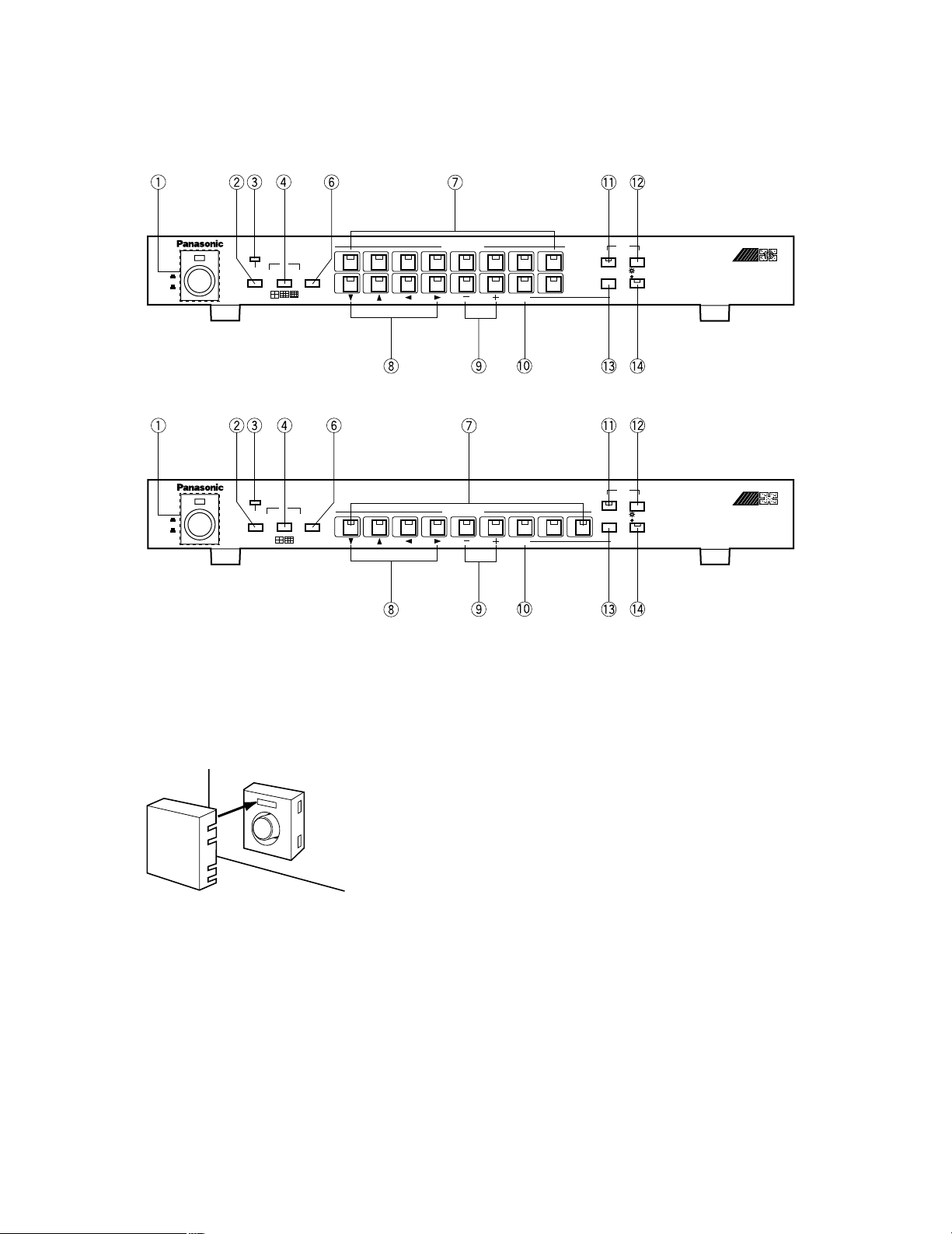
MAJOR OPERATING CONTROLS AND THEIR FUNCTIONS
1
POWER
CAMERA SELECT
SET
ON
OFF
Video Multiplexer WJ-FS
Simplex
SWITCH
PROTECTER
2 3 4 5 6 7 8
9 10 11 12 13 14 15 16
STILL
MENU
ESC
EL-ZOOM
FS
116
VTR
CAM
SEQ
ALARM
RESET
ALARM
VTR
MULTISCREEN
SELECT
VTR
1
POWER
CAMERA SELECT
SET
ON
OFF
Video Multiplexer WJ-FS
SWITCH
PROTECTER
2 3 4 5 6 7 8 9
STILL
MENU
ESC
FS
109
VTR
CAM
SEQ
MULTI SCREEN
SELECT
ALARM
RESET
ALARM
9
VTR
VTR
Simplex
EL-ZOOM
■ Front View
<WJ-FS116>
<WJ-FS109>
q Power Switch (POWER ON / OFF)
This switch turns the power of the video multiplexer on
or off. The LED lights up when the power is turned on.
Note: To prevent that the power of the video multiplexer
is turned off accidentally, install the supplied switch
protector as shown below.
SWITCH
PROTECTOR
wAlarm Reset Button (ALARM RESET)
This button resets the active Alarm mode. Pressing this
button turns off the Alarm indicator and replaces the
“Alarm” indication on the monitor screen with the camera
title.
e Alarm Indicator (ALARM)
This indicator (Red) blinks when an alarm is activated. It
changes to steady light when the auto-reset time has
elapsed or the alarm recovery signal is received from the
VTR. To turn the indicator off, press the ALARM RESET
button.
r Multiscreen Selection Button (MULTISCREEN
SELECT)
This button selects the multiscreen pattern for the monitor. Multiscreen is available only while the VTR is in
playback mode. Pressing this button repeatedly switches
patterns as follows:
VTR Playback Picture:
4→9→16→4 screen segments (WJ-FS116)
4→9→4 screen segments (WJ-FS109)
Notes:
• This button does not function in recording mode.
• When ON is selected for QUAD SHIFT on the MONITOR OUTPUT SETUP menu, the screen changes
by pressing this button as follows:
4A→4B→4C→4D→9→16 screen segments
(WJ-FS116)
4A→4B→9 screen segments (WJ-FS109)
The 4A screen is a compressed picture of channels
1 through 4, the 4B of channels 5 through 8, the 4C
of channels 9 through 12, and the 4D of channels 13
through 16. The 9-segment screen shows the pictures of channels 1 through 9 in a 3x3 pattern.
y Sequence Button (SEQ)
This button activates the sequence mode. In this mode,
a series of camera pictures is displayed in succession
on the monitor screen for the specified duration.

– 2 –
u Camera Selection Buttons (CAMERA SELECT)
These buttons select the camera for live picture or picture recorded on the tape. When the VTR is in playback
mode and the LED on the VTR/CAM Selection button is
on, these buttons select the specified camera picture
from the tape for display on the monitor. When the LED
is off, the buttons select the live picture of the specified
camera.
i Cursor Buttons (C, D, A, B)
These buttons move the cursor in the SETUP MENU of
the Video Multiplexer, or select an area for Electronic
Zooming.
C: Downward
D: Upward
A: Left
B: Right
o Increment/Decrement Buttons (–, +)
Electronic Zooming is operated with these buttons,
Zoom In with the + button and Zoom Out with the – but-
ton. During the setup, these buttons are used to select
parameters.
!0 Set Button (SET)
This button executes the selected parameter in the
setup menu, and opens a submenu for more detailed
settings. Menu items having a submenu are identified by
a return symbol at the end of the line.
!1 Still Button (STILL)
This button selects either still or moving mode for display
of the VTR playback on the monitor. Pressing a Camera
Selection button will display the corresponding picture
either in still or moving mode. When a still picture is displayed, the LED (Green) lights. Pressing the button
again restores the moving picture and turns off the LED.
Note: Please note that the tape continues running while
the picture is stilled. You may sometimes have to
rewind the tape to the desired position.
!2 Electric Zoom Button (EL-ZOOM)
This button specifies the zooming area in the playback
picture. Pressing this button displays the “+” sign representing the centre of the area to be enlarged. While the
“+” sign is displayed for 5 seconds, move the “+” sign
with the cursor buttons to the desired position and press
the Increment (+) button. The designated area is
enlarged.
To return to the normal picture press the Decrement (–)
or the EL-ZOOM button.
!3 MENU/ESC Button (MENU/ESC)
Pressing this button for 2 seconds or more opens the
Setup Menu of the Video Multiplexer. If pressed for less
than 1 second, it functions as the Escape button and
returns you to the previous menu.
To close the Setup menu when the setup is completed,
press the button for 2 seconds.
Notes:
• Make sure to distinguish between 1-second and 2second operation of this button.
• Opening the Setup menu does not affect the recording signal (REC OUT) output from the rear panel.
!4 VTR/Camera Selection Button (VTR/CAM)
This button selects either VTR playback or the camera
picture for display on the monitor. At the same time, it
disables or enables recording on the VTR, since the
connected VTR performs only playback or recording at a
time. The playback picture is displayed on the monitor if
you start playing back the VTR while the LED (Green) is
on. The camera picture is displayed on the monitor while
the LED is off. The camera picture is recorded on the
tape if you start the VTR recording.
Notes:
• If PLAYBACK AUTO is set to ON in the setup,
pressing this button is ignored, instead this button
follows the VTR status automatically. VTR is selected while playing back, and CAMERA is selected during non-playback mode of the VTR.
• There may be a delay of few seconds after switching
this button between VTR and CAMERA when PLAYBACK AUTO is ON.
• Blinking of the LED is a warning that the ID code is
missing in the playback signal. This may happen
when using certain VTR types. In this case, the playback picture goes straight to the monitor instead of
through the Video Multiplexer. As a result, the playback picture will not be recognizable unless only a
single channel is recorded throughout the tape.
– 3 –
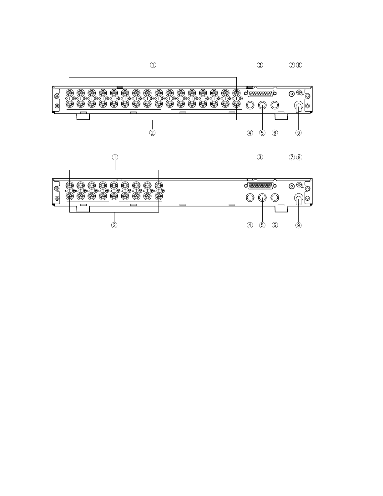
SIGNAL
GND
ALARM/REMOTE
OUT
IN
VIDEO
16 15 14 13 12 11 10 9 8
16 15 14 13 12 11 10 9 8
7654 21
76543321
PLAY IN
REC OUT
CAMERA
SW IN
MONITOR OUT
SIGNAL
GND
ALARM/REMOTE
OUT
IN
VIDEO
987 6 543 21
987 6 543 21
PLAY IN
REC OUT
CAMERA
SW IN
MONITOR OUT
■ Rear View
<WJ-FS116>
<WJ-FS109>
q Video Input Connectors (VIDEO IN)
These connectors accept a composite video signal from
a camera.
Note: If the input signals have a high jitter content, as in
the case of a VTR playback picture, it may not be
possible to synchronize this unit.
w Video Output Connectors (VIDEO OUT)
The video signals connected to the Video Input
Connectors (VIDEO IN) are looped through to these
connectors with an automatic 75 Ω termination.
e Alarm / Remote Control Connector (ALARM /
REMOTE)
This connector accepts the alarm signals from the associated alarm sensor units and the control signals from
the external system.
r Playback Input Connector (PLAY IN)
The playback signal from the time lapse VTR is supplied
to this connector.
t Record Output Connector (REC OUT)
The recording signal for the time lapse VTR is provided
via this connector.
y Monitor Output Connector (MONITOR OUT)
The video output signal for the monitor is provided via
this connector.
u Camera Switching Input Connector
(CAMERA SW IN)
The camera switching pulse from the time lapse VTR is
supplied to this connector.
The camera switching interval (Sequential Dwell Time)
can be synchronized with the time lapse mode set in the
associated time lapse VTR.
i Signal Ground Terminal (SIGNAL GND)
o Power Cord
– 4 –
ADJUSTMENT PROCEDURE
1. Test Equipments Required
8
The following Test Equipments are required for
adjustment of the Video Multiplexer WJ-FS109/WJ-FS116.
8
Underscanned Colour Video Monitor
8
Waveform Monitor
8
Video Signal Generator
Ramp Signal (without Carrier)
Sweep Signal or Multi Burst Signal (more than 10MHz)
8
Oscilloscope
8
Frequency Counter
8
Ceramic Screwdriver
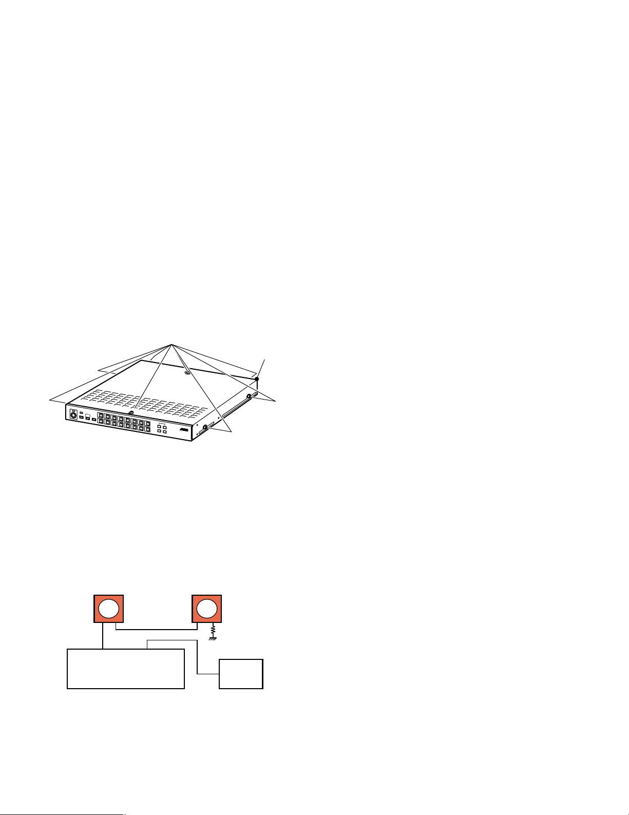
2. Disassembling Procedure for the Adjustment
8
Referring to Fig. 2-1, remove eight screws that secure the
Upper Cover and remove the Upper Cover.
Fig. 2-1
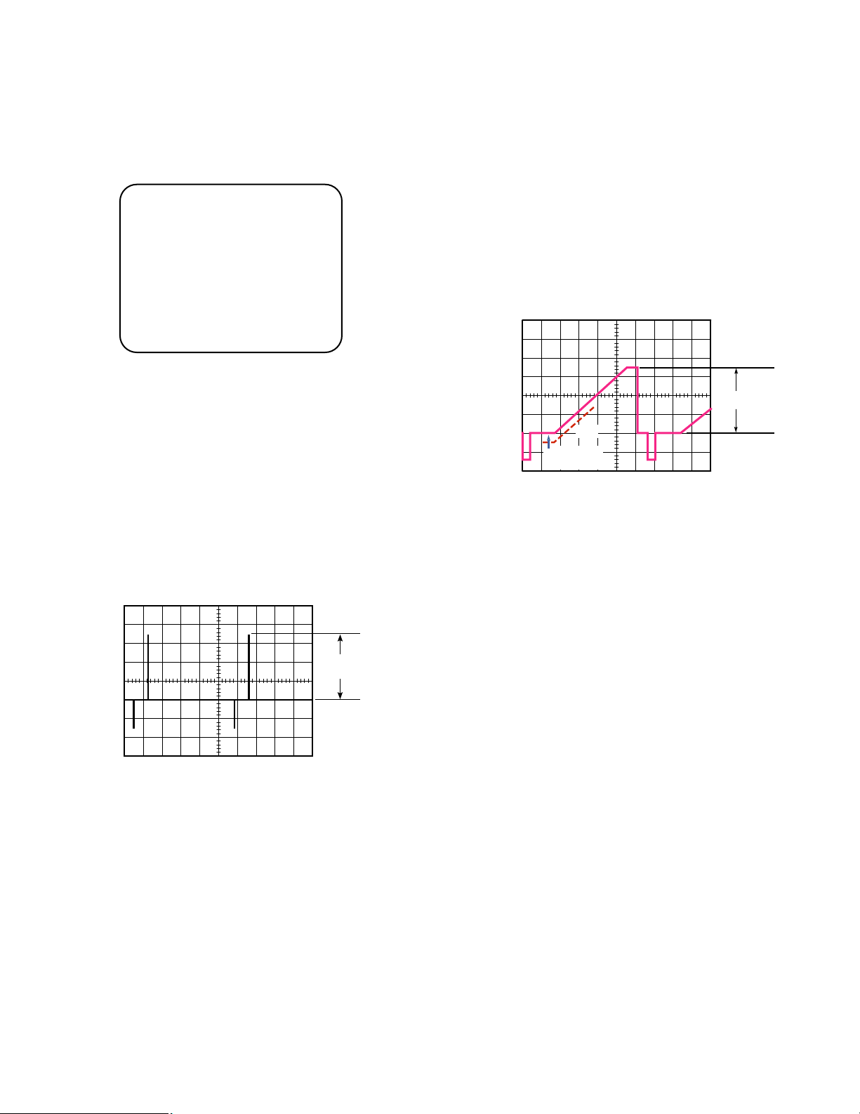
3. Connection and Setting up for Adjustment
3.1. Connection
8
Fig. 3-1 shows the connecting diagram for adjustment of
the WJ-FS109/WJ-FS116.
Fig 3-1
Remove eight screws.
Upper Cover
8
Connect the Underscanned Colour Video Monitor through
the Waveform Monitor to the Record Output Connector on
the Rear Panel of the WJ-FS109/WJ-FS116.
8
Terminate the input terminal of the Underscanned Colour
Video Monitor with 75 Ω.
8
Connect the Signal Generator to the Video Input
Connector 1 on the Rear Panel of the WJ-FS109/WJFS116.
8
Connect the probe of the Oscilloscope or Frequency
Counter at the desired Test Point in each adjustment step.
3.2. Setting Up
8
This adjustment should be done after 30 minutes warm up
of the WJ-FS109/WJ-FS116.
<Initial Setting>
8
Before start to adjust should be done with this Initial
Setting as follows:
8
Turn the Power Switch off.
8
Turn the Power Switch on while pressing the CURSOR
Button (
5), the DECREMENT Button (–) and MENU
Button simultaneously, all LEDs on the Front Panel are lit
and enter to the Initial Mode.
8
Turn the Power Switch off.
4. Adjustment Procedure
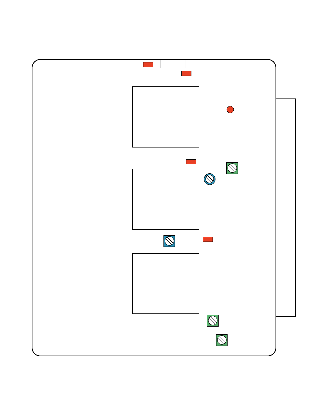
8
Refer to the Location of the Test Points and
Adjusting Controls on the page 6.
(1). 13.5MHz Frequency Adjustment
Test Point: TP505 (13.5MHz) Main Board
Adjust: CT500 (13.5MHz) Main Board
8
Disconnect all input signals from the WJ-FS109/WJFS116.
8
Connect the Frequency Counter to TP505 and TP307
(GND).
1
VIDEO IN
REC OUT
WJ-FS109/WJ-FS116
Video
Signal
Generator
Waveform
Monitor
Underscanned
Colour Video Monitor
75 Ω
– 5 –
8
Turn the Power Switch on while pressing the CURSOR
Button (
5), the INCREMENT Button (+) and MENU button
simultaneously, enter the Adjustment Mode and all LEDs
on the Front Panel are lit, and display the Adjustment
Menu as shown in Fig. 4-1.
Fig. 4-1
8
Adjust CT500 to obtain 13.500000 MHz ± 18 Hz.
(2). ID Level Adjustment
Test Point: Record Output Connector Rear Panel
Adjust: VR501 (ID LEVEL) Main Board
8
Connect the terminated Oscilloscope with 75Ω to the
Record Output Connector on the Rear Panel.
8
Trigger the oscilloscope at V rate.
8
Adjust VR501 so that the ID level becomes 700 ± 15 mVpp as shown in Fig. 4-2.
Fig. 4-2
(3). G/L PLL DC Level Adjustment
Test Point: TP508 (G/L PLL DC) Main Board
Adjust: L500 (G/L PLL DC) Main Board
8
Supply the Ramp signal to the Video Input Connector 1 on
the Rear Panel.
8
Connect the Oscilloscope to TP508.
8
Set the Input Selector of the Oscilloscope to DC Mode.
8
Adjust L500 to obtain 2.0 ± 0.3 V DC.
(4). Y Level Adjustment and Y Pedestal Adjustment
Test Point: Record Output Connector Rear Panel
Adjust: VR400 (Y-GAIN) Main Board
VR404 (Y-PEDESTAL) Main Board
8
Supply the Ramp signal to the Video Input Connector 1
on the Rear Panel.
8
Connect the terminated Oscilloscope with 75Ω to the
Record Output Connector on the Rear Panel.
8
Adjust VR404 so that the Luminance Pedestal level
becomes 0 mV as shown in Fig. 4-3.
8
Adjust VR400 so that the Luminance level becomes 700 ±
15 mVp-p as shown in Fig. 4-3.
Fig. 4-3
REC 01CH
700 ±
15 mVp-p
700 ± 15 mVp-p
(0 mV)
+ 7
– 0
NG
+ 7
– 0
– 6 –
VR400
(Y-GAIN)
VR501
(ID LEVEL)
VR404
(Y-PEDESTAL)
L500
(G/L PLL DC)
TP508
(G/L PLL DC)
TP505
(13.5MHz)
TP307
(GND)
TP701
(+5V)
TP700
(–5V)
CN700
CT500
(13.5MHz)
B N C
REAR SIDE
FRONT SIDE
MAIN BOARD (COMPONENT SIDE)
LOCATION OF TEST POINTS AND ADJUSTING CONTROLS
– 7 –
BNC BOARD
(Component Side)
DSUB BOARD
(Component Side)
MAIN BOARD
(Component Side)
FRONT BOARD
(Component Side)
POWER BOARD
(Component Side)
E1
18
E3
81
E1
121
E2
131
CN304
1113
CN301
12 1
CN302
CN700
CN300
13 1
15
81
CN717
18
14
CN303
114
E2
E1
13 1
CN1
15
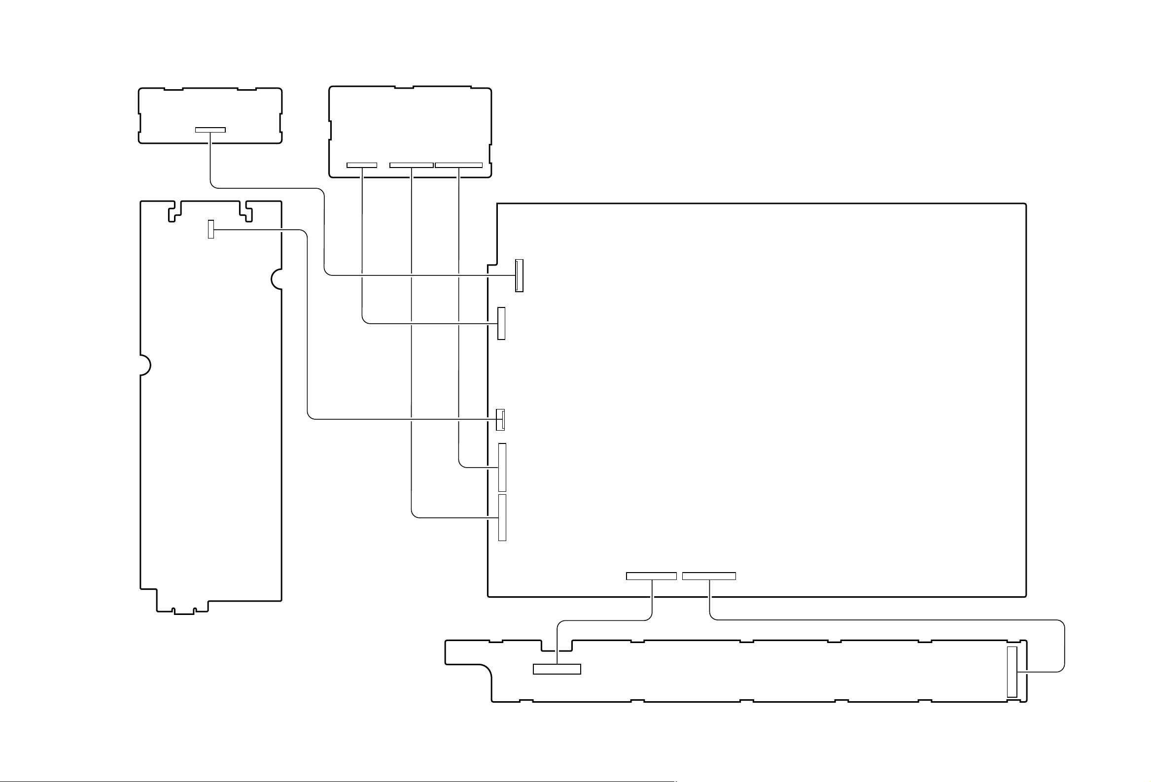
WIRING DIAGRAM
FS116C01A
FS916E01A
K1PA12C00001
K1PA14C00001
K1PA02C00002
K1PQ13D00001 (WJ-FS116)
K1PA06C00003 (WJ-FS109)
ELY322V513 (WJ-FS116)
ELY122V511 (WJ-FS109)
BUFFER
Q707
CN701
BUFFER
Q708
CN702
BUFFER
Q709
CN703
BUFFER
Q710
CN704
BUFFER
Q711
CN705
BUFFER
Q712
CN706
BUFFER
Q713
CN707
BUFFER
Q714
CN708
BUFFER
Q715
CN709
9
8
7
6
5
4
3
2
1
IC701 SELECTOR
3
013
COM
114
215
312
41
55
62
74
CH9
CH8
CH7
CH6
CH5
CH4
CH3
CH2
CH1
X
CH3
CH4
CH5
CH6
CH7
CH8
CH9
C
B
A
INH
9
10
11
6
DETA
DETB
DETC
IC703 SELECTOR
3
013
COM
114
215
312
41
55
62
74
Y
CH3
CH5
CH6
CH7
CH8
CH9
C
B
A
INH
9
10
11
6
14X
0X12
1X13
IC700(a)
SELECTOR
15Y
0Y2
1Y1
4
Z
0Z5
1Z3
IC700(b)
SELECTOR
RDSYNC
DETD
MOND
RECD
1
COM
A
07
16
5
MBLK
C
9
PHNL
11A
10B
PLAY
DRIVER
Q700-Q703
Q725
BUFFER
Q726-Q728
c
a
IC709
IC709
6
5
2
1
#HSYNC
20
#VSYNC
19
IC707 SWITCH
14X
0X12
1X13
IC710
SELECTOR
15Y
0Y2
1Y1
11A
10B
4Z
0Z5
1Z3
9C
BUFFER
Q406
CHDET
CH DETECTOR
IC708,Q704-Q706
AMP.
CLAMP
YB7
YB7
4FSC
4FSC
Q403-Q405
TRAP
L400,L401,
C423-C425,
R450,R451
VR400
(Y-GAIN)
VR404
(Y-PEDESTAL)
BUFFER
Q400,Q401
BUFFER
Q425
VIN
19
IC400
Y. A/D
CONVERTER
D0-D7
3-10
CLK
12
IC603
VIDEO SIGNAL
PROCESSOR
IC502
GATE ARRAY LOGIC
IC801
GATE ARRAY LOGIC
IC800
EEPROM
142-149
YIB0-YIB7
IC503 D-RAM
MA0-MA15
157-161,163,
165-174
2-5,7-10,
31-34,36-39
I/O0-I/O15
MMA0-MMA15
A0-A8
ADD0-ADD8
124-131,133
16-19,22-26
28
29
14
13
#UCAS
#LCAS
#RAS
#WE
#OE
27
IC504 D-RAM
MB0-MB15
135-146,148,
152-154
2-5,7-10,
31-34,36-39
I/O0-I/O15
MMB0-MMB15
A0-A8
16-19,22-26
28
29
14
13
#UCAS
#LCAS
#RAS
#WE
#OE
27
1
2
3
4
W4FSCB
56
201-208
A YCIN0-A YCIN7
DATA
DCLK
OE
#CS
IDSEP IN
PD0-PD7
AD0-AD4
PCSN
AD6
DOB0-DOB7
DATA
VCLK
nSTATUS
CONF_DONE
31-38
125
WVP
129
128
56
105
RHD
15
X500,
CT500 (13.5MHz)
D/A CONVERTER
YO0-YO7
66-73
Q504,R574-R590
MIX
Q505
RSYNC
61
VR501
(ID LEVEL)
RDSYNC
R SYNC
DRIVER
DRIVER
Q508
Q506
Q509,Q510
REC OUT1
IC302
MICROPROCESSOR
P20/DB0-P27/DB7
33-40
150
ADCKB
P00/AD0-P07/AD7
P10/AD8-P17/AD15
41-56
AN0-AN3
18-21
AD0-AD6
AD0
AD4
AD6
AD0-AD3
AD0-AD3,AD4M,AD6
93-98
PA0-PA4
PCSN
1
2
3
4
5
6
7
8
9
10
11
12
13
GND
GND
RECOVER IN
SEQ
ALARM OUT
SELECT2
ALARM10
ALARM14
ALARM11
ALARM15
ALARM12
ALARM16
ALARM13
CN302
To D-Sub Board
. . . . . . . . . . E2
81-88
PD0-PD7
DB0-DB7
8-10,13-17
PW0-PW7PW0-PW7
3,5,7,9,12,
14,16,18
A1-A4
B1-B4
YA1-YA4
YB1-YB4
2,4,6,8,11,
13,15,17
IC308
TRANSCEIVER
1
2
3
A0
A1
A2
IC306
3-8 DECODER
Y1
Y2
Y4
Y5
Y6
Y7
14
13
11
10
9
7
1
2
3
A0
A1
A2
IC307
3-8 DECODER
CS3
Y2
Y0
Y1
Y4
Y5
5
13
15
14
11
10
CS1
GA
GB
6
4
5
6
4
7
9
CS1
CS2
Y7
Y6
P36/#WR
58
P37/#RD
57
5V
#RD
#WR
RY1
RY2
RY4
RY5
RY6
IC705 SELECTOR
3
013
COM
114
215
312
41
55
62
74
Z
X
X
Z
CH2
CH1
CH3
CH4
CH5
CH6
CH7
CH8
CH9
Q723
Q729,Q603
C
B
A
INH
9
10
11
6
a
2
1
3
IC300
b
4
5
6
IC300
IC317
1
2
4
IC506
c
10
9
8
IC300
d
13
12
5
1
11
6
IC300
DETA
DETB
DETC
DETD
MONA
MONB
MONC
MOND
Y0WR
Y1WR
Y4WR
Y5WR
12
15
16
19
RECA
RECB
RECC
RECD
Y6WR
AD4R
AD4M
AD4F
AD6F
AD7F
AD5F
AD0-AD10 AD0-AD10
PW0-PW7
PW4-PW7
DB0-DB7
DB0-DB7DB0-DB7
DB0-DB7
#WR
#WR
AD7
AD4
AD6
AD7
AD5
AD4M
AD13
AD9
AD8
AD7
AD14
AD15
AD13
AD11
AD12
EA
1
EB
19
DO
CS
SK
DI
IC301
EEPROM
4
1
2
3
11
7
9
10
P70/SIN2
P74
P72/SCLK2
P71/SOUT2
IC309
VOLTAGE DETECTOR
BUFFER
Q300
Q724
27
#RESET
2
IN
OUT
6
7
Vcc
5V
SRESET CRESET
Y6WR
92
PWRN
I/O0-I/O8
11-13,15-19
IC304
D-RAM
A0-A10
3-10,21,24,25
#WR
#RD
RY1
CRESET
#WE
#DE
#OE1
#OE2
CK
Q4
Q5
Q6
Q7
IC316
LATCH
D4-D7
13,14,
17,18
11
27
22
20
26
1
2
3
4
5
6
7
8
9
10
11
12
ALARM1
GND
ALARM2
ALARM5
ALARM3
ALARM6
ALARM4
ALARM7
SELECT1
ALARM8
RECOVER OUT
ALARM9
CN301
To D-Sub Board
. . . . . . . . . . E1
1
2
3
4
5
6
7
8
9
10
11
12
13
14
+5V
PW0
PW1
PW2
GND
PW3
PW4
PW5
ALARM
Y4WR
Y0WR
GND
Y1WR
+5V
CN303
To Front Board
. . . . . . . . . . E1
1
2
3
4
5
6
7
8
9
10
11
12
13
GND
DB0
DB1
DB2
DB3
DB4
DB5
AD4
GND
AD6
AD7
SPLED
AD5
CN304
To Front Board
. . . . . . . . . . E2
1
2
3
4
5
6
1
2
4
5
7
8
1
2
3
4
5
6
PLAY IN
GND
REC OUT
GND
MONI OUT
GND
E1 CN717
CN1
Playback
Input
Connector
Record
Output
Connector
Monitor
Output
Connector
IC310 SELECTOR
2
Y04
A0
3B0
5
Y17
A1
6B1
11
Y29
A2
10B2
14
Y312
A3
13B3
OUT
1
15
SEL
IC311 SELECTOR
2
Y04
A0
3B0
5
Y17
A1
6B1
11
Y29
A2
10B2
14
Y312
A3
13B3
OUT
1
15
SEL
IC312 SELECTOR
IC715 DRIVER
2
Y04
A0
3B0
5
Y17
A1
6B1
11
Y29
A2
10B2
14
Y312
A3
13B3
OUT
1
15
18 2
SEL
AD7
RY4
AD7
RY4
AD7
RY5
RY2
DB0
DB1
DB2
DB3
DB4
DB5
DB6
DB7
DB0
DB5
DB1
DB2
DB3
AMP.
PHNL
5V
ALARM
Y4WR
Y0WR
Y1WR
AD6F
AD7F
SPLED
AD5F
AD4F
ROUT
PW0
PW1
PW2
PW3
PW4
PW5
PW0-PW5
FSC
RCOIN
33
MADD0-MADD8
CAS
119
RAS
123
WE
118
OE
117
Q301,Q303
SW300
DRIVER
Q302
CAMSW
ALAO
DRIVER
P77
ALARM
5
P76
15
P54/CONTR0
12CAMERA SW
GND
CN300
To D-Sub Board
. . . . . . . . . . E3
ALAO
PLAY
BUFFER
PBSYNCBUFFER
REC OUT
MONI OUT
REIN
SEQ
SEL2
AL10
AL14
AL11
AL15
AL12
AL16
AL13
AL1
AL2
AL5
AL3
AL6
AL4
AL7
SEL1
AL8
AL9
1
2
3
4
5
+5VA
GND
+5VD
GND
–5V
CN700
To Power Board
. . . . . . . . . . E1
+5VA
+5VD
–5V
AL1
AL5
AL2
AL6
AL3
AL7
AL4
AL8
AL9
AL13
AL10
AL14
AL11
AL15
AL12
AL16
SEL2
AL9
SEQ
REIN
SEL1
Q402
VIDEO IN
IC804
SYNC SEPARATOR
6
VC
VS
9
10
5
SYNC OUT
16
HOUT
DELAY AWPLLHD
RSYNC
PHNLWVP
AWPLLHD
IC805(f),(e)
10
13
PBHRL
16
P53/INT4
BUFFERCAMSW
17
P52/INT3
4
HIN
198
AWPLLHD
SRESET
77
RESET
187
234
A EN
B EN
VCO
RSCIN
47
RSCO
45
RSCOUT
48
RCOOUT
34
Q501,D502,
D503,X501
PLL
IC507,IC508,Q500,
Q507,D500,D501,
L500 (G/L PLL DC)
TP508 (G/L PLL DC)
TP701
TP700
A WCOIN
195
A WCOOUT
A CPOUT
A W4FSC
A WVCOD
196
183
185
199
a
IC805
2
1
d
IC805
IC606
IC605
IC604
8
9
e
11
10
d
IC405
8
9
IC405
b
3
4
IC805
c
5
6
IC805
5V
5V
5V
–5V
5V
5V
5V
193
A WSYNC
CHDET
28
P41
19
P50
RVP
41
RHDO
40
RVP
RHDI
42
BZ300
VIN1
VIN3
VIN2
5
1
3
7VOUT
2CONT1
4
CONT2
13
P56/DA1
24
P43/INT1
68
P84
67
P85
66
P86
65
P87
3
P60/AN0
2
P61/AN1
1
P62/AN2
80
P63/AN3
13
BLK2
16
VR
1
CLK
3
DATA
2
#CS
IC712
CHARACTER GENERATOR
8
P73/#SRDY2
4
#PCL
RECOUT
RECOUT1
MONI OUT
CRESET
FHAB
50
194
A WFHA
WFCKB
51
50
R4FSC
TP505 (13.5MHz)
R13M
65
SEPAID
191
131-138
109,110,
112,113,
115
116
WFHA
8
Y5WR
WE
7
CHSL
4
178
A VCOIN
181
A PLLVDD
138
VPINB
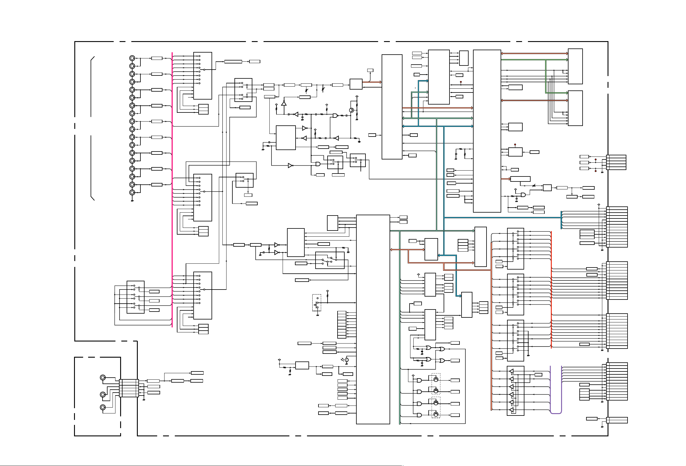
BLOCK DIAGRAM OF WJ-FS109
MAIN BOARD
18
P51/INT2
IDON
14
P55/CONTR1
PHNL
MBLK
12
4
Q305
DRIVER
P75
ROUT
6
P57/DA2
25
P42/INT0
RVP
IDON
76
IDON
SPLED
63
P31
12
Y6WR
PWRN
121
PBHRL
PBHRL
124
PBSYNC
PBSYNC
29
WVP
WVP
IDSEP OUT
10
RVP
14
RVP
R13M
20
A W27MO
175
W27M
17
Video
Input /
Output
Connectors
MONA
MONB
MONC
RECA
RECB
RECC
BNC BOARD
1
4
2
IC802
Q800
1
COM
A
07
16
5
1
4
2
16 4
1
19
DB4
14 6
DB3
12 8
DB2
911
DB1
713
DB0
DB5
DB4
DB3
DB2
DB1
DB0
DB0
DB1
DB2
DB3
DB4
DB5
1
3
2
b
IC317
4
6
5
c
IC317
10
8
9
d
IC317
13
11
12
Q307
Q306
4
2
3
5
1
6
4
2
3
5V
– 8 –
 Loading...