

Panasonic WJAVE-55 Service manual
SPECIFICATIONS
Source Input : x4 (SOURCE 1/4)
Video Input : 1.0 Vp-p/75Ω PAL composite signal, pin-jack
Y/C input: Y signal : 1.0 V[p-p]/75Ω, C signal : 0.3 V[p-p]/75Ω Mini Din 4-pin connector
Audio Input : –6 dBs 20 kΩ pin jack (L/R)
Character Input : x1 (TITLE) ; 10-pin connector for optional Character Generator WJ-TTL7
Recording Output : x1 (REC OUT )
Video Output : 1.0 Vp-p/75Ω PAL Composite signal, pin-jacks
Y/C Output : Y signal ; 1.0 V[p-p]/75Ω, C signal ; 0.3 V[p-p]/75Ω Mini Din 4-pin connector
Audio Output : –6 dBV/1 kΩ, pin jacks (L/R)
Preview Output :
Video Output : 1.0 Vp-p/75Ω PAL Composite signal, pin-jacks
Back Colour : White, Yellow, Cyan, Green, Magenta, Red, Blue,Black and Useable
Wipe Patterns : 157 patterns
Video Gain : Unity
S/N (typical) : Video 50 dB (composite), 50 dB (Y/C)
Audio ; 60 dB
Power Source : 220 - 240V AC, 50 Hz
Power Consumption : Approx 19W
Ambient Operating Temperature : 0°C - 40°C (32°F - 104°F)
Ambient Operating Humidity : Less than 90%
Dimensions: 420 (W) x 300 (H) x 88 (D) mm
Weight: 2.5 kg
Weight and dimensions indicated above are approximate.
Specifications are subject to change without notice.
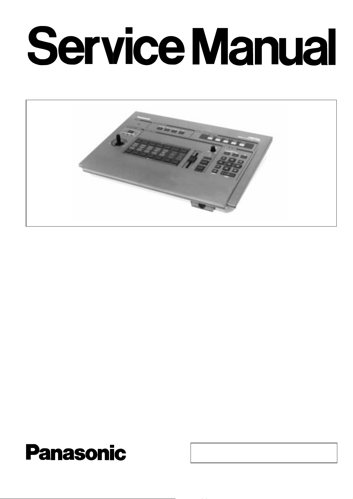
Digital AV Mixer
WJ-AVE55
ORDER NO. AVS9602118C8
C 1996 Matsushita Communication Industrial Co., Ltd.
All rights reserved. Unauthorized copying and
distribution is a violation of law.
This service information is designed for experienced repair technicians only and is not designed for use by the
general public.
It does not contain warnings or cautions to advise non-technical individuals of potential dangers in attempting to
service a product.
Products powered by electricity should be serviced or repaired only by experienced professional technicians. Any
attempt to service or repair the product or products dealt with in this service information by anyone else could
result in serious injury or death.
!
WARNING
CAUTION
RISK OF ELECTRIC SHOCK
DO NOT OPEN
CAUTION:
TO REDUCE THE RISK OF ELECTRIC SHOCK,
DO NOT REMOVE COVER (OR BACK). NO USER
SERVICEABLE PARTS INSIDE.
REFER SERVICING TO QUALIFIED SERVICE
PERSONNEL.
This symbol warns the user that uninsulated voltage within
the unit may have sufficient magnitude to cause electric
shock. Therefore, it is dangerous to make any kind of contact
with any inside part of this unit.
This symbol alerts the user that impotant literature concerning
the operation and maintenance of this has been included.
Therefore, it should be read carefully in order to avoid
any problems.
There are special components used in this equipment which are important for safety. These parts are indicated
by the ” Y ” mark on the schematic diagram and the replacement parts list. It is essential that these critical
parts should be replaced with manufacturer's specified parts to prevent shock, fire, or other hazards.
Do not modify the original design without permission of manufacture.
IMPORTANT SAFETY NOTICE
CONTENTS
MAJOR OPERATING CONTROLS AND THEIR FUNCTIONS........................................................................................... 1
SYSTEM CONNECTION ...................................................................................................................................................... 5
CIRCUIT DESCRIPTION
IC DESCRIPTION.............................................................................................................................................................. 6
ADJUSTMENT PROCEDURE..............................................................................................................................................27
LOCATION OF TEST POINTS AND ADJUSTING CONTROLS.........................................................................................30
APPEARANCE OF IC,TRANSISTOR AND DIODE.............................................................................................................31
CHIP COMPONENTS...........................................................................................................................................................32
BLOCK DIAGRAM
SWITCH BOARD...............................................................................................................................................................34
MAIN BOARD(1/2).............................................................................................................................................................35
MAIN BOARD(2/2).............................................................................................................................................................36
SCHEMATIC DIAGRAM
MAIN BOARD(2/2).............................................................................................................................................................38
MAIN BOARD(1/2).............................................................................................................................................................40
SWITCH BOARD...............................................................................................................................................................41
POWER BOARD................................................................................................................................................................41
CONDUCTOR VIEW
MAIN BOARD ....................................................................................................................................................................37
SWITCH BOARD...............................................................................................................................................................41
POWER BOARD................................................................................................................................................................41
EXPLODED VIEW ................................................................................................................................................................42
REPLACEMENT PARTS LIST.............................................................................................................................................43
Standard Accessory Optional Accessory
Power Cord 1 pc. Character Generator WJ-TTL7
1
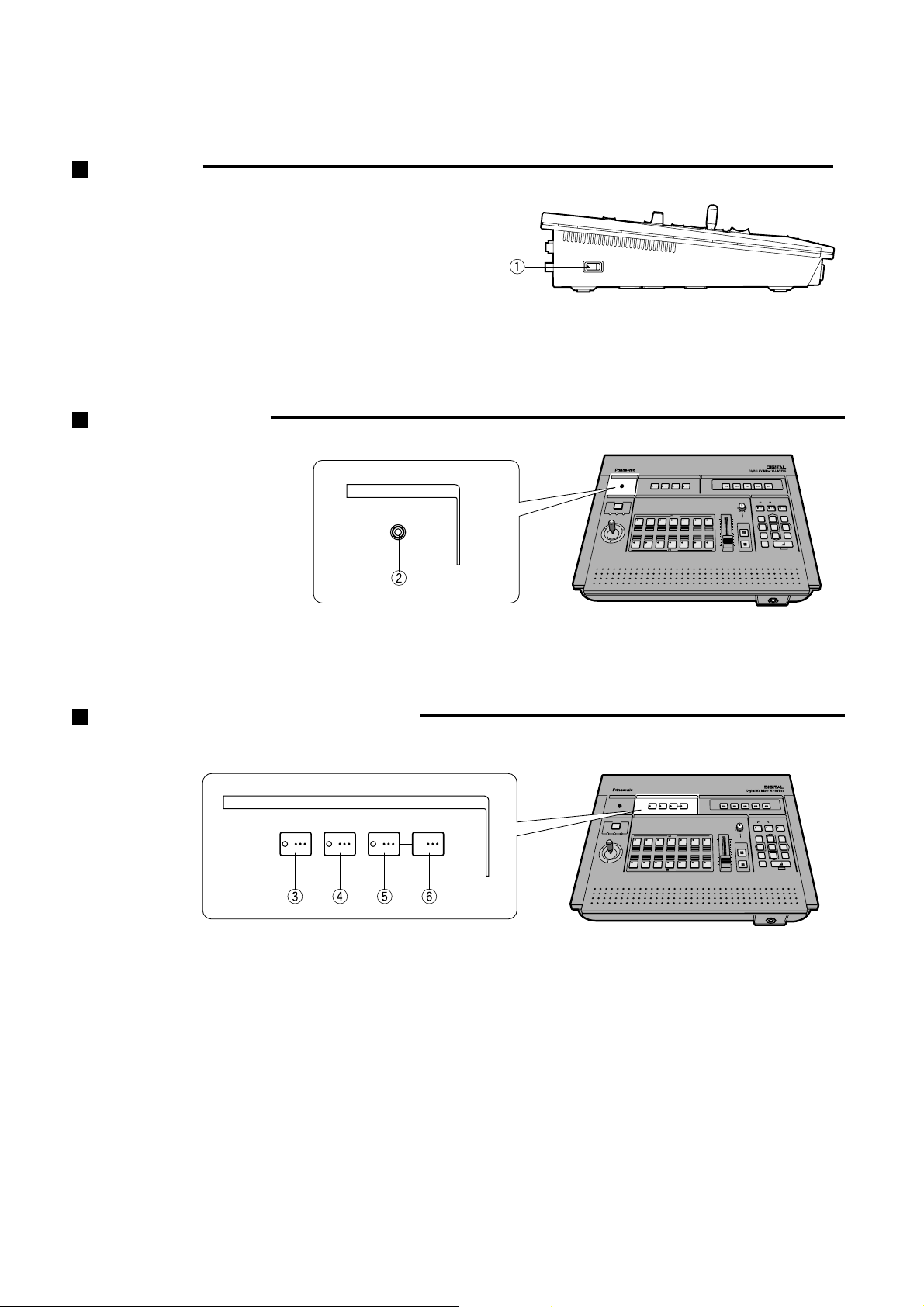
POWER Section
(2) Power Indicator
Side View
(1) Power Switch (POWER ON/OFF)
(3) Wipe / Mix Selection Button (WIPE/MIX)
Used to select either the Wipe or Mix Effect.
Lighting : shows the Wipe selection
Blinking : shows the Mix selection
(4) Luminance Key Button
Used to replace certain luminance of one picture with a
second picture.
TRANSITION SELECT Section
POWER
OFFON
POWER
TRANSITION SELECT
WIPE/MIX
LUM KEY CHROMA KEY
SET
(5) Chroma Key Button
Used to replace certain colour of one picture with a
second picture.
(6) Set Button
Used to select the position for the chroma function.
MAJOR OPERATING CONTROLS AND THEIR FUNCTIONS
2
ON SCREEN DISPLAY SETTING Section
ON SCREEN DISPLAY SETTING
WIPE EFFECT COL. FADE AUDIO
(7) Wipe Button (WIPE)
Used to display the Wipe menu on the preview monitor.
(8) Effect Button (EFFECT)
Used to display the Effect Setting menu on the preview
monitor.
(9) Colour Button (COL.)
Used to select the colour for the back screen or wipe
edge.
(10) Fade Button (FADE)
Used to display the Fade Setting menu on the preview
monitor.
(11) Audio Button (AUDIO)
Used to display the Audio Setting menu on the preview
monitor.
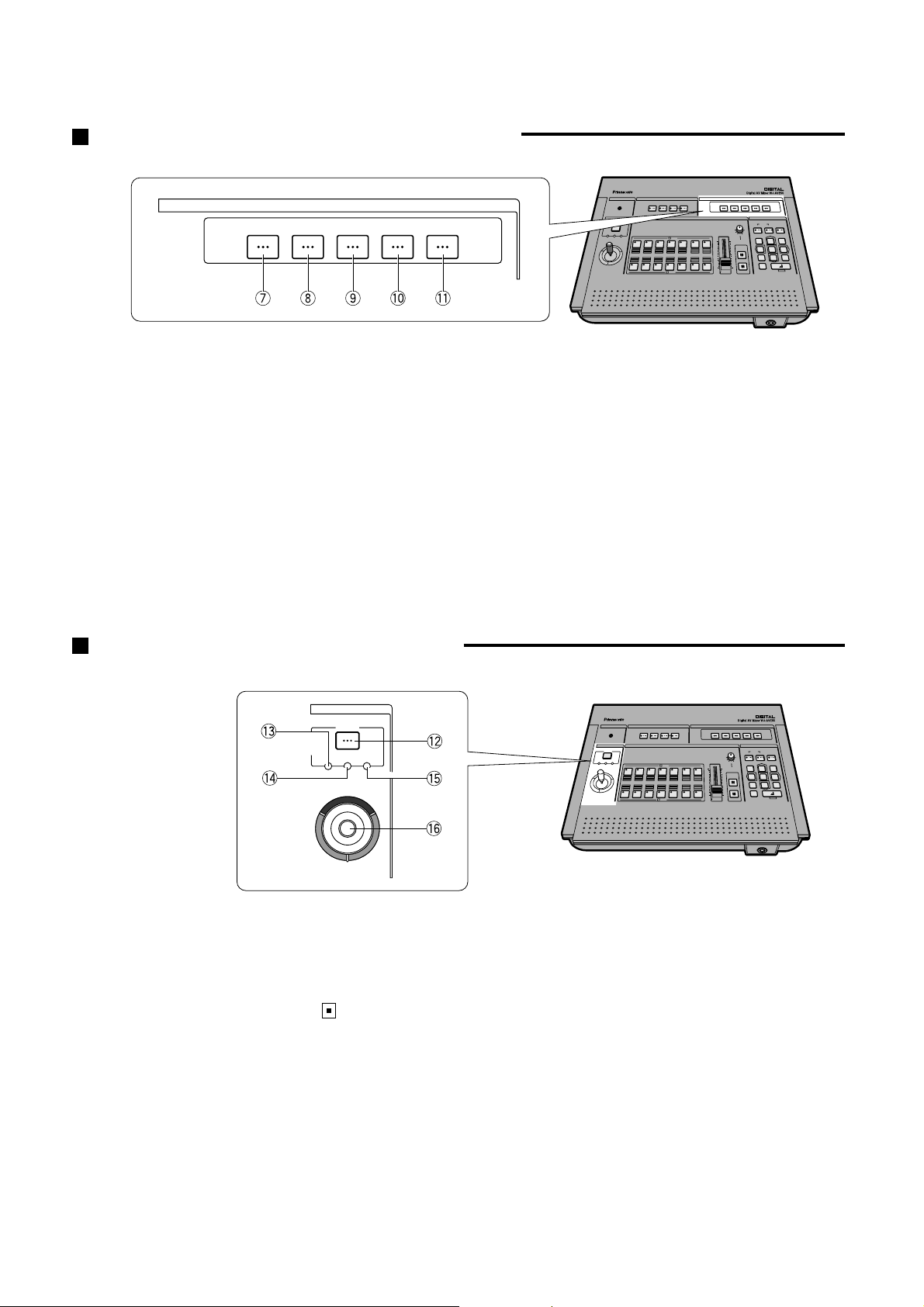
POSITION/COL. CORRECT Section
POSITION/COL.CORRECT
SELECT
POSITION GRABBER
SCENE
CORRECT
COL.
R
GB
(14) Scene Grabber Indicator (SCENE. GRA.)
(15) Colour Correct Indicator (COL CORRECT)
(16) Joystick Control
This joystick Control has two functions - setting the
position of the specified wipe pattern , moving the cursor for setting the chroma key and correcting the
Colour A-bus / B-bus.
(12) Select Button (SELECT)
Used to select the POSITION, SCENE GRABBER or
COL CORRECT.
Notes :
1. Scene Grabber is available in pattern.
2. When selecting the CHROMA ON mode and press
the desired Effect Output Button, colour correction
is available.
(13) Position Indicator (POSITION)
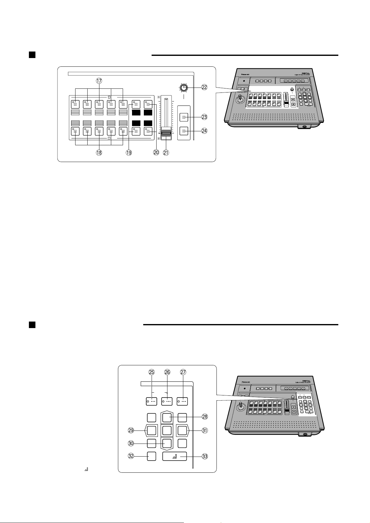
3
(20) Still Out Buttons (STILL)
An instant still or frozen image can be obtained by
pressing this button.
(21) Mix/Wipe Control (MIX WIPE EFFECT)
Mix and wipe can be performed by operating this control.
(22) Time Control (TIME)
For adjusting the transition time of Auto Fade Function
and Auto Take Function.
(23) Auto Fade Button (AUTO FADE)
Automatic fade can be executed according to the time
set by TIME Control.
(24) Auto Take Button (AUTO TAKE)
Automatic wipe or mix can be executed according to
the time set by TIME Control (22).
SOURCE SELECT Section
SOURCE SELECT
SOURCE1SOURCE2SOURCE3SOURCE4BACK
COL.
EFFECT STILL
A BUS
B BUS
AUTO FADE
AUTO TAKE
TIME
MIN MAX
14
2
8
(17) A-bus Selection Buttons (A)
SOURCE 1: Used to select Source 1 Audio/Video
Signals (35)(36)(37) supplied to the rear panel.
SOURCE 2: Used to select Source 2 Audio/Video
Signals (38)(39)(40) supplied to the rear panel.
SOURCE 3: Used to select Source 3 Audio/Video
Signals (41)(42)(43) supplied to the rear panel.
SOURCE 4: Used to select Source 4 Audio/Video
Signals (44)(45)(46) supplied to the rear panel.
BACK COL: Used to select the Back Colour.
(
18) B-bus Selection Buttons
Same selection can be available as mentioned in the Abus Selection buttons (17).
(19) Effect Out Buttons (EFFECT)
Used to supply the effect signal to the preview and Rec
Out connectors.
MODE SETTING Section
MODE SETTING
MEMORY CALL No.
EVENT
1 2 3
4 5 6
7 8 9
0
SELECT
/UNDO
(25) Event Memory Button (EVENT MEMORY)
Used to memorize the present status.
(26) Call Button (CALL)
Used to recall the
memorized status.
(27) Number Button (No.)
(28) Up Button
(29) Left Button
(30) Down Button
(31) Right Button
(32) SELECT/UNDO Button
(33) Enter Button ( )
4
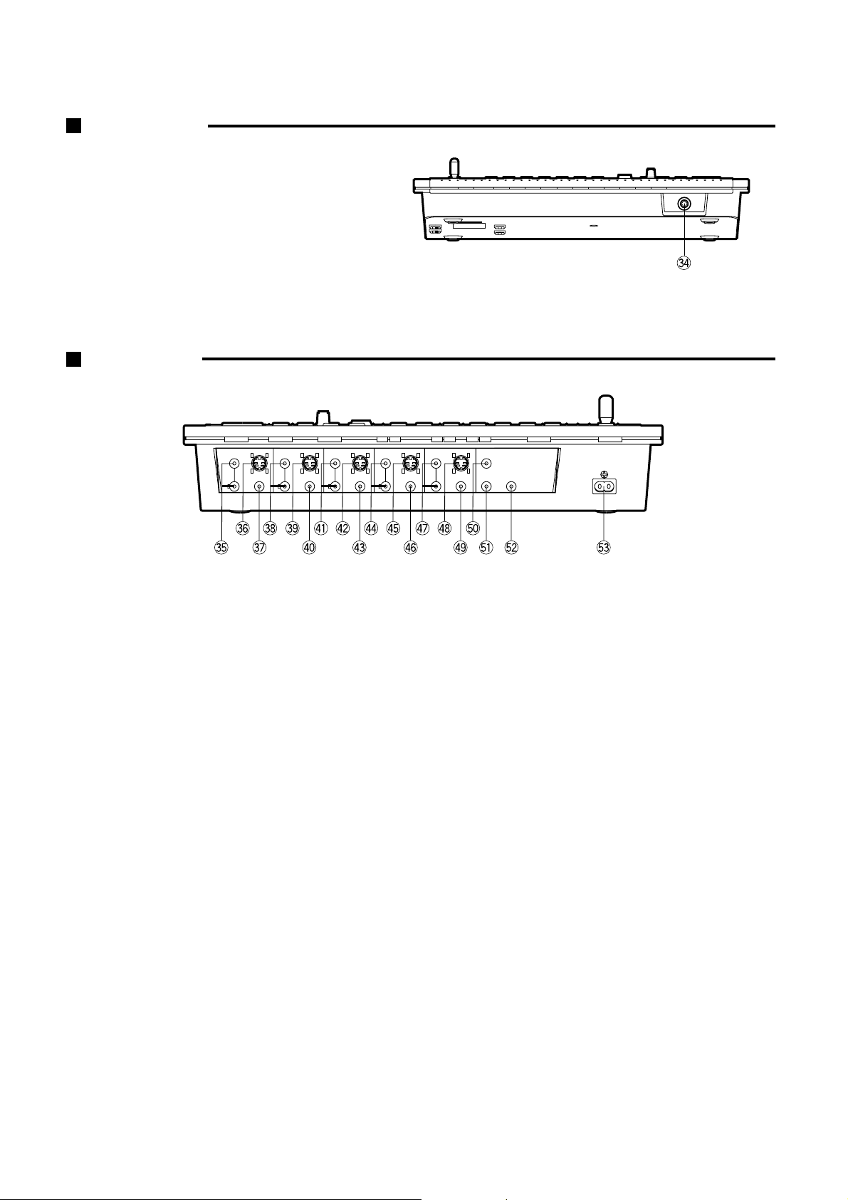
Front Panel
(34) Titler Connector (TITLE)
TITLE
Rear Panel
COMP
Y/C
SOURCE 1
AUDIO
L
R
COMP
Y/C
SOURCE 2
AUDIO
L
R
COMP
Y/C
SOURCE 3
AUDIO
L
R
COMP
Y/C
SOURCE 4
AUDIO
L
R
COMP
Y/C
REC OUT
AUDIO
L
R
SERIAL
GPI
PREVIEW
-AC IN
(35) Source 1 Audio Input Jack (SOURCE 1 AUDIO)
(36) Source 1 S-video Input Connector (Y/C)
(37) Source 1 Composite Video Signal Input Jack
(38) Source 2 Audio Input Jack (SOURCE 2 AUDIO)
(39) Source 2 S-video Input Connector (Y/C)
(40) Source 2 Composite Video Signal Input Jack
(41) Source 3 Audio Input Jack (SOURCE 3 AUDIO)
(42) Source 3 S-video Input Connector (Y/C)
(43) Source 3 Composite Video Signal Input Jack
(44) Source 4 Audio Input Jack (SOURCE 4 AUDIO)
(45) Source 4 S-video Input Connector (Y/C)
(46) Source 4 Composite Video Signal Input Jack
(47) Recording Out Audio Output Jack
(REC OUT AUDIO)
(48) Recording Out S-video Output Connector
(REC OUT Y/C)
(49) Recording Out Composite Video Signal
Output Jack
(50) GPI Connector (GPI)
Refer to the qualified service personnel or system
Installers for this connection.
(51) Preview Output Connector
Connect to video input connector of the preview monitor.
(52) Serial Connector (SERIAL)
Refer to the qualified service personnel or system
Installers for this connection.
(53) Power Socket (AC IN)
Connect the Power Cord (provided) to this socket.
5
SYSTEM CONNECTION
Q Composite (RCA-style) video and audio
W S-video (Y/C)
Types of Input and Output Jacks
Y/C
SOURCE 1
AUDIO
L
Q W
Preview Monitor
Output Monitor
Power
Cord
WJ-TTL7
L
R
AUDIO
SOURCE 1
Y/C
COMP
L
R
SOURCE 2
AUDIO
Y/C
COMP
L
R
SOURCE 3
AUDIO
SOURCE 4
AUDIO
L
Y/C
COMP
R
Y/C
COMP
REC OUT
Y/C
COMP
GPI
PREVIEW
SERIAL
-AC IN
AUDIO
L
R
6
2. Main Board
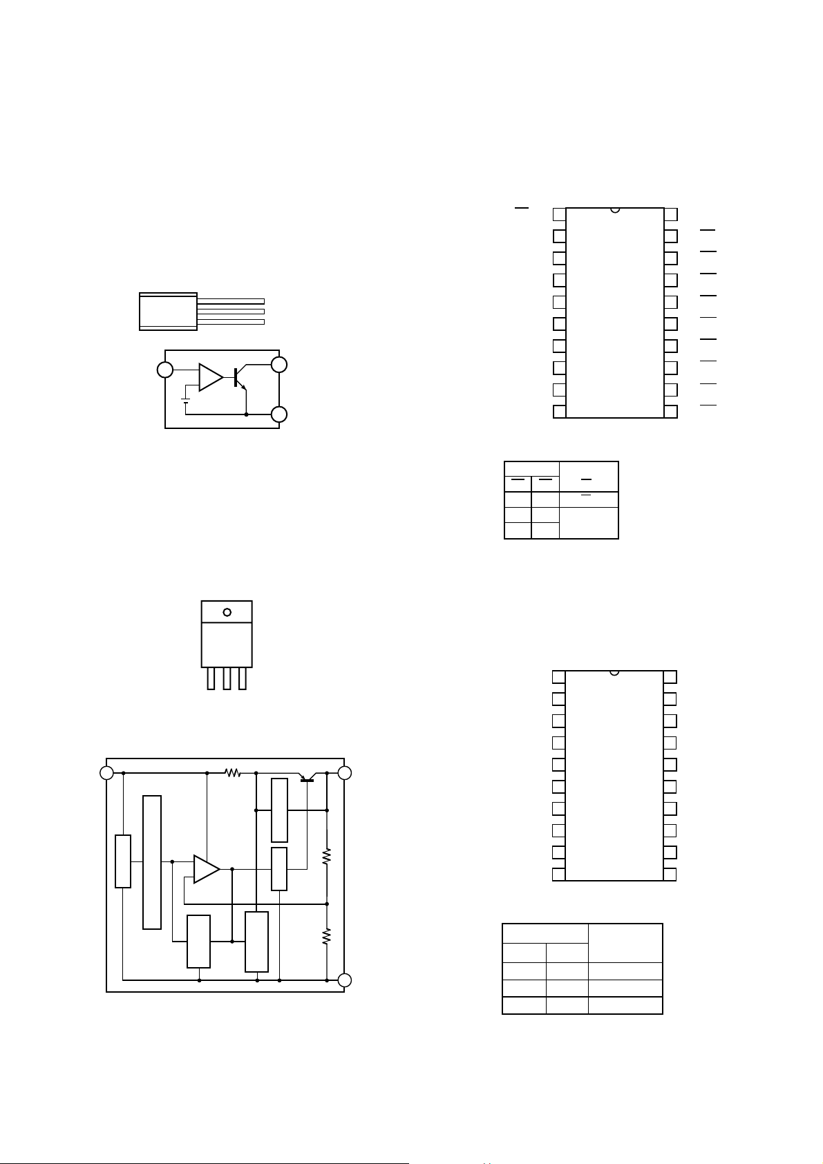
2.1. IC1 on the Main Board is using the Octal 3-State Bus
Buffers IC MC74HC541AF.
Description of this IC is as follows:
2.2. IC6 and IC7 on the Main Board are using the Octal 3-
State D-FFs IC MC74HC374AF.
Description of this IC is as follows:
IC Description
1. Power Board
1.1. IC2 on the Power Board is using the Variable Shunt
Regulator IC YWTA76431S.
Description of this IC is as follows:
1.2. IC1 on the Power Board is using the-3-terminal
Voltage Regulator IC YWUPC24M12HF.
Description of this IC is as follows:
CIRCUIT DESCRIPTION
1 Reference
2 Anode
3 Cathode
+
–
1
3
2
Reference
Cathode
Anode
Input 1
GND 2
Output 3
ASO Limiter
Starter
Reference Voltage Generator
Driver
Over-current
Protector
Over-heat
Protector
1
3
2
Error
Amp.
Input
Output
GND
E1 1
1A 2
2A 3
3A 4
4A 5
5A 6
6A 7
7A 8
20 Vcc
19 E2
18 1Y
17 2Y
16 3Y
15 4Y
14 5Y
13 6Y
(TOP VIEW)
E2
L
INPUTSYOUTPUT
: Don’t care.
Z : High Impedance
H
E1
L
H
A
Truth Table
8A 9
GND 10 11 8Y
12 7Y
Z
∗
∗
∗
1Q 2
1D 3
2D 4
2Q 5
3Q 6
3D 7
4D 8
20 Vcc
19 8Q
18 8D
17 7D
16 7Q
15 6Q
14 6D
13 5D
(TOP VIEW)
4Q 9
GND 10 11 EG
12 5Q
OE 1
INPUTS
FUNCTION
EG
Latch
Q = D
: Don’t care.
Truth Table
OE
HZ
Z : High Impedance
L
H
∗
∗
∗
∗
7
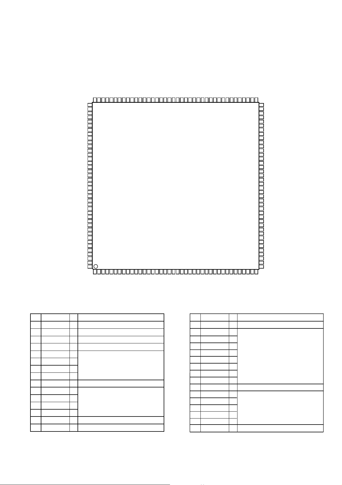
2.3. IC62 on the Main Board is using the 2-D Low Pass Filter HCMOS Gate Array Logic IC YWAJ0016.
Description of this IC is as follows:
Y3C 1
Vss 2
HPC 3
FS4 4
RECC0 5
RECC1 6
RECC2 7
RECC3 8
V
DD 9
RECC4 10
RECC5 11
RECC6 12
V
DD 25
SD0 26
SD1 27
SD2 28
SD3 29
SD4 30
Vss 31
PVWC0 32
PVWC1 33
PVWC2 34
PVWC3 35
VDD 36
RECY7 24
RECY6 23
RECY5 22
RECY4 21
RECY3 20
RECY2 19
RECY1 18
RECY0 17
V
DD 16
Y2C 15
Vss 14
RECC7 13
PVWC4 37
PVWC5 38
PVWC6 39
PVWC7 40
41 SPC
42 Vss
43 OS1
44 SD5
45 XHI
46 V
DD
47 PVWY0
48 PVWY1
49 PVWY2
50 PVWY3
51 PVWY4
52 PVWY5
53 PVWY6
54 PVWY7
55 Vss
56 V
DD
57 ASYNC
58 SYNC
59 HD
60 VD
61 VP
62 OSDB
63 OSDG
64 OSDR
65 OSD
66 ST
67 REG5
68 REG4
69 REG3
70 REG2
71 REG1
72 REG0
73 Vss
74 D7
75 D6
76 D5
77 D4
78 D3
79 D2
80 D1
81 D0
82 WPTST
83 TM2
84 TM1
85 TM0
86 PAL
87 MD1
88 MD0
89 SD6
90 WPO
91 V
DD
92 WP1/TD0
93 WP2/TD1
94 WP3/TD2
95 WP4/TD3
96 CH1/TD4
97 CH2/TD5
98 LMRST
99 CHO
100 V
DD
101 CH3/TD6
102 CH4/TD7
103 TD8
104 TD9
105 SD7
106 KBR
107 KBG
108 KBB
109 CHAR
110 SD8
111 AIN7
112 AIN6
113 AIN5
114 AIN4
115 AIN3
116 AIN2
117 AIN1
118 AIN0
119 SHGA
120 Vss
VDD 121
SHGB 122
BIN7 123
BIN6 124
BIN5 125
BIN4 126
BIN3 127
BIN2 128
BIN1 129
BIN0 130
Vss 131
DLC 132
DLY1 133
BGP 135
XBS0 136
TESTOUT 137
EXT0 138
SD9 139
SD10 140
TN 141
XBSI 142
XLS 143
ESY 144
EXT 145
V
DD 146
HS 147
DLY0 148
XH0 149
SD11 150
RST 151
VDD 134
RCLK 152
SD12 153
SD13 154
V
DD 155
YCLK 156
VPN 157
Vss 158
OSC2IN 159
V
DD 160
Pin Name I/O Description
1 Y3C
O Y3C signal output terminal.
2 Vss – Ground terminal.
Pin Name I/O Description
24 RECY7
O
25 V
DD – Power supply terminal.
3 HPC O HPC signal output terminal.
4 FS4 O
FS4 signal output terminal.
5 RECC0
O
7 RECC2
O
6 RECC1
O
8 RECC3 O
9 V
DD – Power supply terminal.
10 RECC4 O
11 RECC5
O
12 RECC6 O
26 SD0
I
27 SD1
I
28 SD2
I
29 SD3
I
18 RECY1
O
19 RECY2 O
20 RECY3 O
21 RECY4
O
22 RECY5
O
23 RECY6
O
17 RECY0 O
(TOP VIEW)
16 VDD – Power supply terminal.
13 RECC7 O
14 Vss
– Ground terminal.
15 Y2C O Y2C signal output terminal.
30 SD4 I
31 Vss – Ground terminal.
REC(Y) signal output terminals.
SD signal input terminals.
REC(C) signal output terminals.
REC(C) signal output terminals.
8
Pin Name I/O Description
32 PVWC0
O
Pin Name I/O Description
89 SD6
I SD signal input terminal.
90 CHOB
O CHOB signal output terminal.
33 PVWC1 O
34 PVWC2
O
35 PVWC3
O
37 PVWC4
O
36 Vss
– Ground terminal.
38 PVWC5 O
39 PVWC6
O
40 PVWC7
O
41 SPC O SPC signal output terminal.
42 V
DD – Power supply terminal.
91 V
DD – Power supply terminal.
92 WP1/TD0
I
93 WP2/TD1
I
94 WP3/TD2
I
83 TM2
I
84 TM1
I
85 TM0
I
86 PAL
I PAL signal input terminal.
87 MD1
I
88 MD0
I
82 WPTST I WPTST signal input terminal.
43 OS1I I OS signal input terminal
44 SD5
I SD signal input terminal.
45 XHI I XH signal input terminal.
95 WP4/TD3 I
46 VDD – Power supply terminal.
47 PVWY0 O
48 PVWY1
O
49 PVWY2 O
50 PVWY3 O
51 PVWY4 O
52 PVWY5
O
53 PVWY6 O
54 PVWY7 O
55 Vss – Ground terminal.
56 V
DD – Power supply terminal.
57 ASY O ASY signal output minals
58 SYC O SYC signal output terminas.
61 VP O VP signal output terminals.
59 HD O HD signal output terminal.
60 VD O VD signal output terminal.
62 OSDB I OSDB signal input terminal.
63 OSDG I OSDG signal input terminal.
64 OSDR I OSDR signal input terminal
65 OSD
I OSD signal input terminal.
66 ST I Strobe signal input terminal.
67 REG5
I
68 REG4 I
69 REG3
I
70 REG2 I
71 REG1 I
72 REG0 I
73 Vss
– Ground terminal.
74 DATA7
I
75 DATA6 I
76 DATA5 I
77 DATA4 I
78 DATA3
I
79 DATA2 I
80 DATA1 I
98 LMRST O LMRST signal output terminal.
100 VDD – Ground terminal.
96 CH1/TD4 I
97 CH2/TD5
I
99 CHOA O CHOA signal output terminal.
101 CH3/TD6 I
102 CH4/TD7 I
103 TD8
I
107 KBG I Green signal input terminal.
108 KBB
I Blue signal input terminal.
109 CHAR I Character signal input terminal.
110 SD8
I SD signal input terminal.
111 AIN7
I
104 TD9
I
105 SD7 I SD signal input treminal.
106 KBR
I Red signal input terminal.
115 AIN3 I
116 AIN2
I
117 AIN1 I
118 AIN0
I
119 SHGA
I SHGA signal input treminal.
112 AIN6
I
113 AIN5
I
114 AIN4
I
120 Vss – Ground terminal.
121 VDD I Power supply terminal.
123 BIN7 I
127 BIN5 I
128 BIN2
I
129 BIN1 I
131 Vss
– Ground terminal.
124 BIN6 I
125 BIN5 I
126 BIN4 I
81 DATA0 I
130 BIN0 I
Preview(C) signal output terminals.
Preview(C) signal output terminals.
Preview(Y) signal output terminals.
Register signal input terminals.
TM signal input terminals.
MD signal input terminals.
TD signal input terminals.
TD signal input terminals.
A signal input terminals.
122 SHGB
– SHGB signal input terminal.
B signal input terminals.
DATA signal input terminals.
9
Pin Name I/O Description
132 DLC
O DLC signal output terminal.
133 DLY1 O DLY1 signal output terminal.
134 V
DD – Power supply terminal.
135 BGP
O Burst Gate Pulse output terminal.
137 TESTOUT
O TEST signal output terminal.
136 XBSO
O XBSO signal output terminal.
138 EXT0
O External signal output terminal.
139 SD9
I
140 SD10
I
141 TN
I TN signal input terminal.
142 XBSI
I XBSI signal input terminal.
143 XLS I XLS signal input terminal.
144 XSY
I XSY signal input terminal.
145 EXT I External signal input terminal.
146 VDD – Power supply terminal.
147 HS O HS signal output terminal.
148 DLY0 I DLY0 signal input terminal.
149 XH0
O XH signal output terminal.
150 SD11 I SD signal input terminals.
151 RST
I RST signal input terminal.
152 RCLK
I Clock pulse input terminal.
153 SD12 I
154 SD13
I
155 VDD – Power supply terminal.
156 YCLK O
Clock pulse output terminal.
157 VPN O VPN signal output terminal.
158 Vss – Ground terminal.
159 OS2I I Oscillation signal input terminal.
160 VDD – Power supply terminal.
SD Data input terminals.
SD Data input terminals.
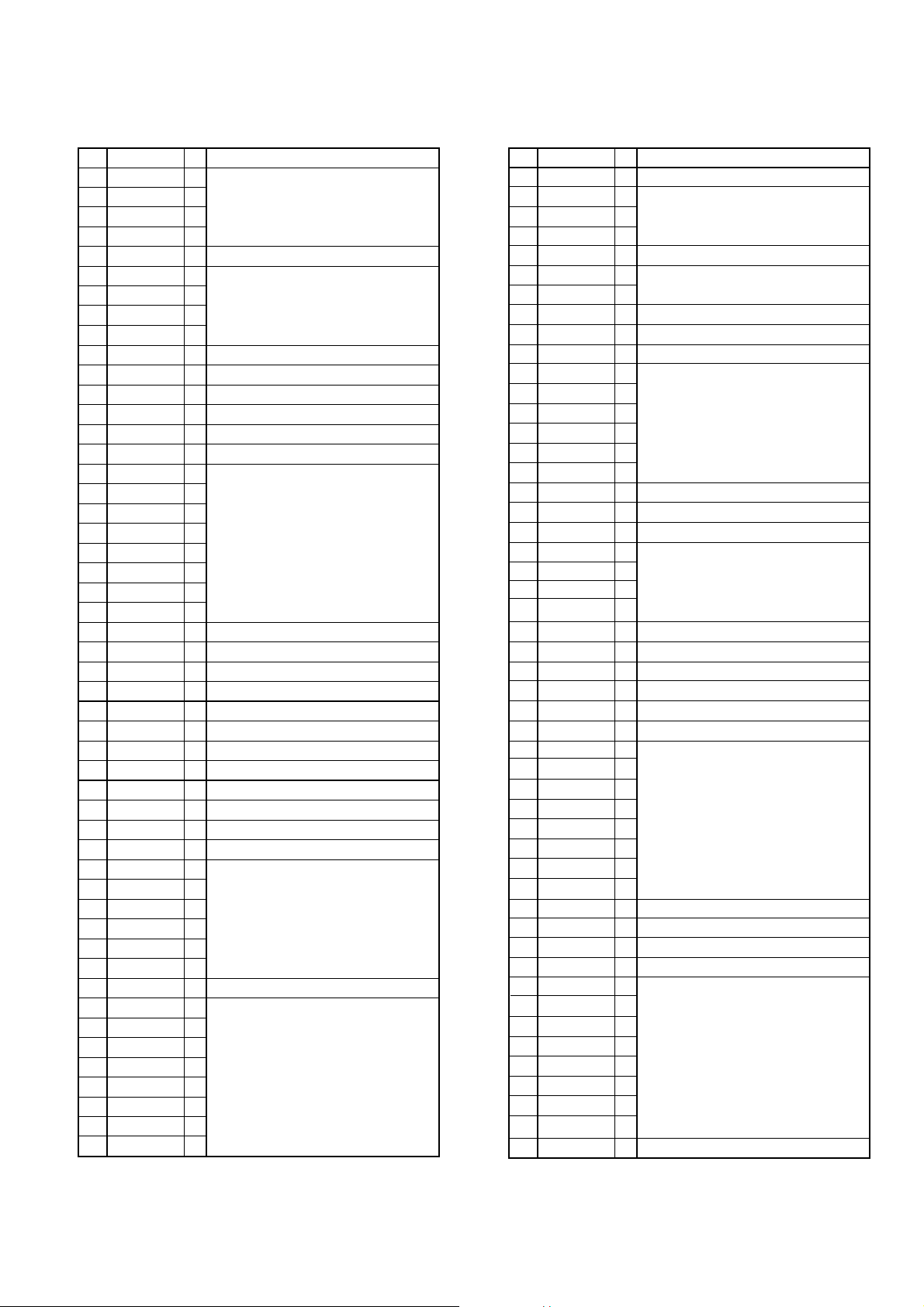
2.5. IC28, IC42 and IC59 on the Main Board are using the
PAL 1,135-word x 8-Bit FIFO High Speed Line Buffers
IC YWUPD42102G3.
Description of this IC is as follows:
(TOP VIEW)
DO0 1
DO1 2
DO2 3
DO3 4
RE 5
RSTR 6
GND 7
RCK 8
DO4 9
DO5 10
DO6 11
DO7 12 13 DI7
14 DI6
15 DI6
16 DI4
17 WCK
18 V
DD
19 RSTW
20 WE
21 DI3
22 DI2
23 DI1
24 DI0
Pin Name I/O Description
1 DO0
O
2 DO1
O
3 DO2
O
4 DO3 O
5 RE
I Read Enable signal input terminal.
6 RSTR
I Reset Read pulse input terminal.
7 GND
– Ground terminal.
8 RCK
I Read Clock pulse input terminal.
9 DO4
O
10 DO5
O
11 DO6
O
12 DO7
O
13 DI7
I
15 DI5
I
14 DI6
I
16 DI4
I
17 WCK I Write Clock pulse input terminal.
18 V
DD – Power supply terminal.
19 RSTW
I Reset Write Pulse input terminal.
20 WE
I Write Enable signal input terminal.
21 DI3
I
22 DI2
I
23 DI1
I
24 DI0
I
Data input terminals. (8-Bit)
Data input terminals. (8-Bit)
Data output terminals. (8-Bit)
Data output terminals. (8-Bit)
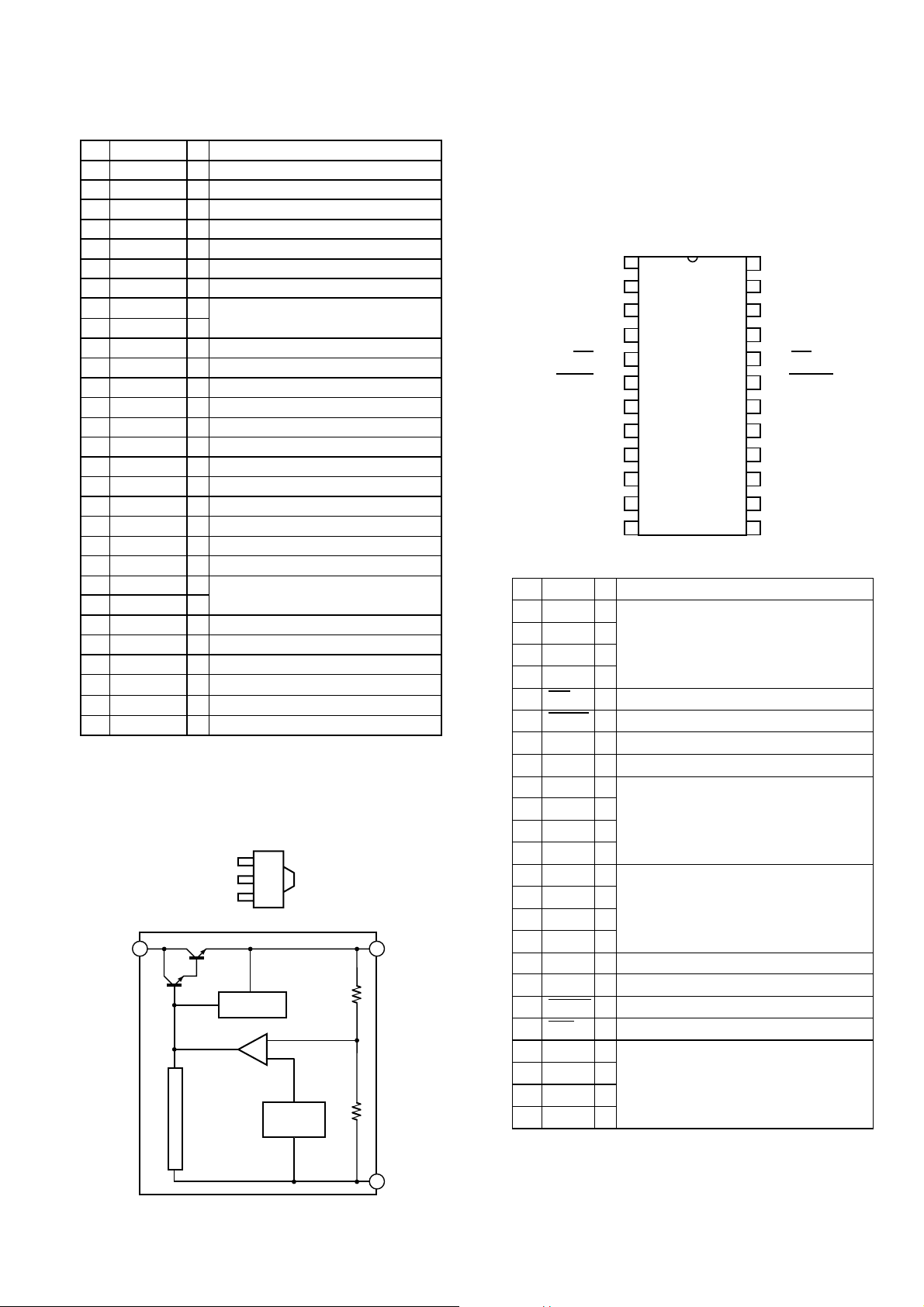
2.4. IC64 on the Main Board is using the 3-Terminal
Voltage Regulator IC YW78L09UATE2.
Description of these IC is as follows:
Output 1
GND 2
Input 3
Reference
Voltage
Generator
Over-current
Protector
Over-heat Protector
3
1
2
Error Amp.
Input
Output
GND
10
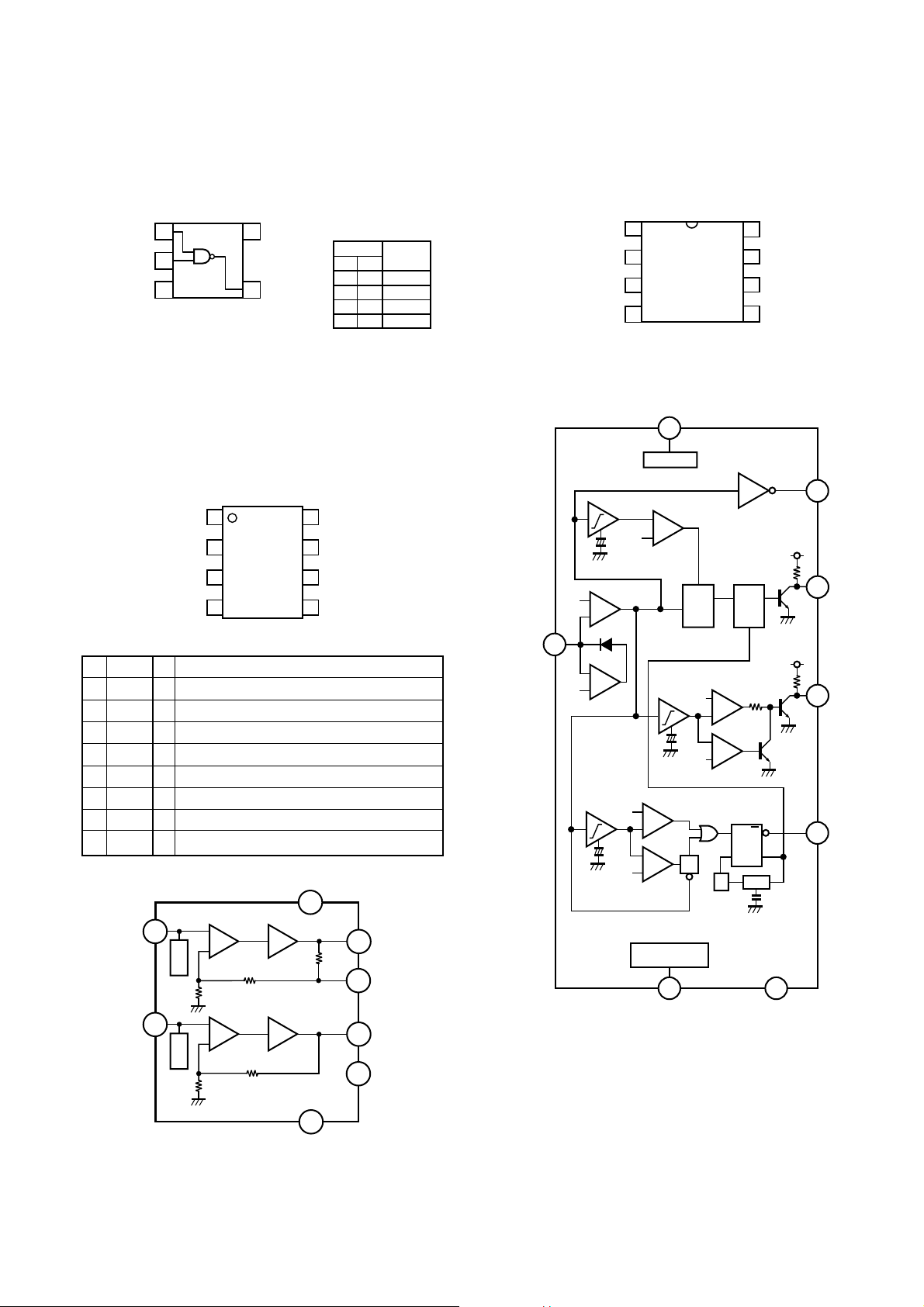
2.8. IC511 and IC512 on the Main Board are using the
Video Sync. Separator IC YWLM1881M.
Description of this IC is as follows:
2.6. IC12, IC47, IC49, and IC50 on the Main Board are
using the Single 2-Input AND Gate IC YWSC7S08F.
Description of this IC is as follows:
2.7. IC14 on the Main Board is using the Dual 6dB Video
Amplifier IC with 75Ω Driver YWNJM2268V.
Description of this IC is as follows:
5 Vcc
4 OUT
IN1 1
IN2 2
GND 3
(TOP VIEW)
Output
L
H
L
H
H
H
H
L
L
L
H
H
Truth Table
Inputs
IN1 IN2
75 Ω
Driver
6 dB
Amp.
6
3
4
VSAG1
GND
Vcc
BiasClamp
6 dB
Amp.
75 Ω
Driver
2.8K 2.8K
2.2K
750
7
2
8
1
5
8 VIN2
7 Vcc
6 N.C.
5 V
OUT2
V
IN1 1
GND 2
V
SAG1 3
V
OUT1 4
(TOP VIEW)
VIN1
V
IN2
V
OUT1
N.C.
V
OUT2
Pin Name I/O Description
1 V
IN1 I Input terminal for Amplifier 1.
2 GND
– Ground terminal.
3 VSAG1 – Sag compensation terminal for Amplifier 1.
4 V
OUT1 O Output terminal for Amplifier 1.
5 V
OUT2 O Output terminal for Amplifier 2.
7 Vcc
– Power supply terminal.
6 N.C.
– Non connection.
8 VIN2 I Input terminal for Amplifier 2.
1
2
3
4
8
7
6
5
Comp.
Sync
GND
V
CC
Odd/Even
Field Index
R
SET
(TOP VIEW)
Video In
Vertical
Sync
Burst/Back
Porch Clamp
R
SET GND
Video
In
V
CC
Comp.
Sync
Odd/
Even
Field
Index
Burst/
Back
Porch
Clamp
Vertical
Sync
VCC
VCC
8
2
1
3
6
+
–
–
+
VA
VB
V
+
–
V1
+
–
+
–
V2
V2
V1
CK
R
Q
CK
Q
D
D
–
+
+
–
SRQ
Q
1/8
OSC
Regulator
–
+
+
–
Capacitor Charge
Current
4
7
5
 Loading...