

Panasonic UNR6224, UNR6223, UNR6222, UNR6221 Datasheet
Transistors with built-in Resistor
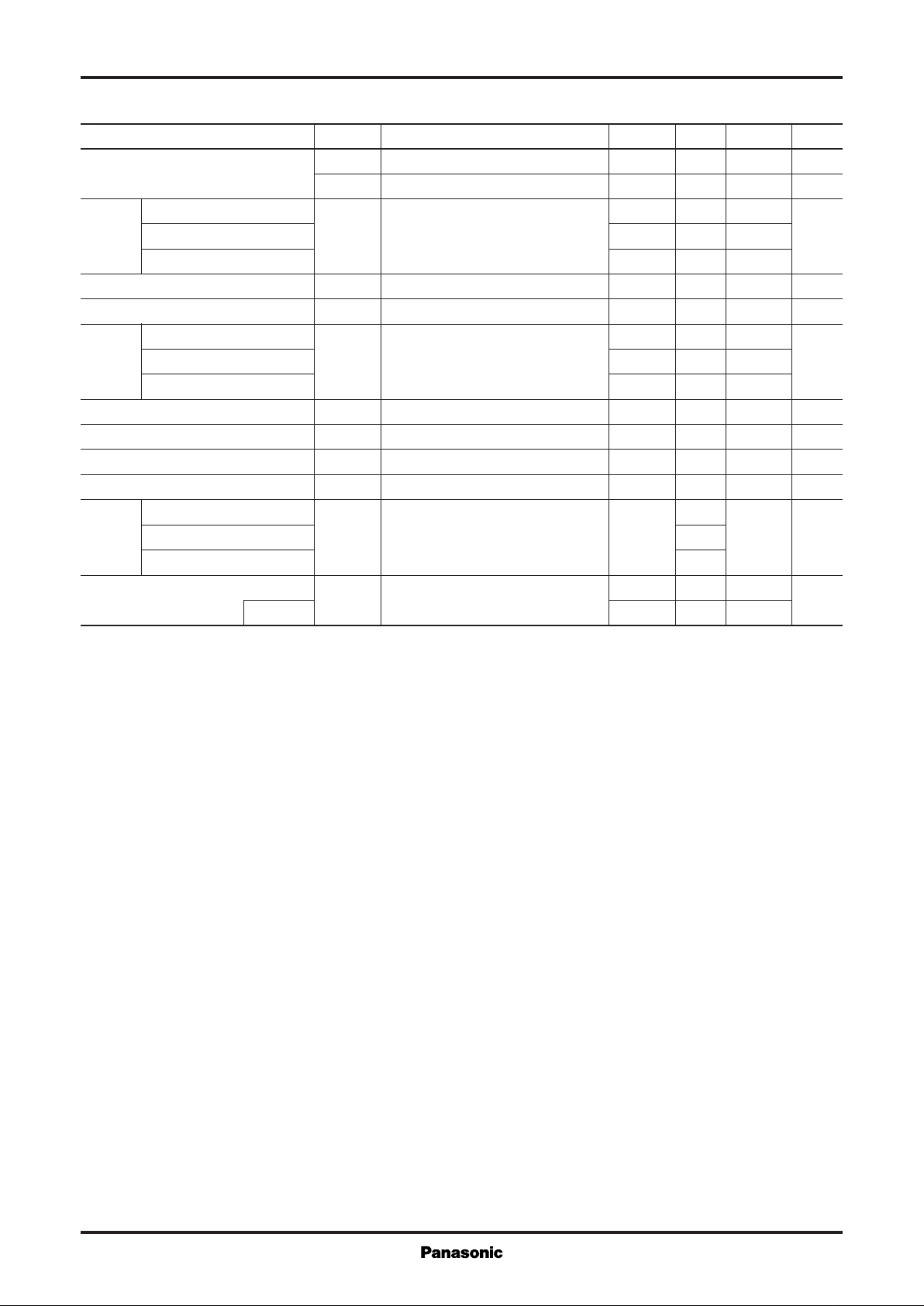
B
C
R1
R2
E
UN6221/6222/6223/6224
Silicon NPN epitaxial planer transistor
For digital circuits
Features
■
●
Costs can be reduced through downsizing of the equipment and
reduction of the number of parts.
●
MT-1 type package, allowing supply with the radial taping.
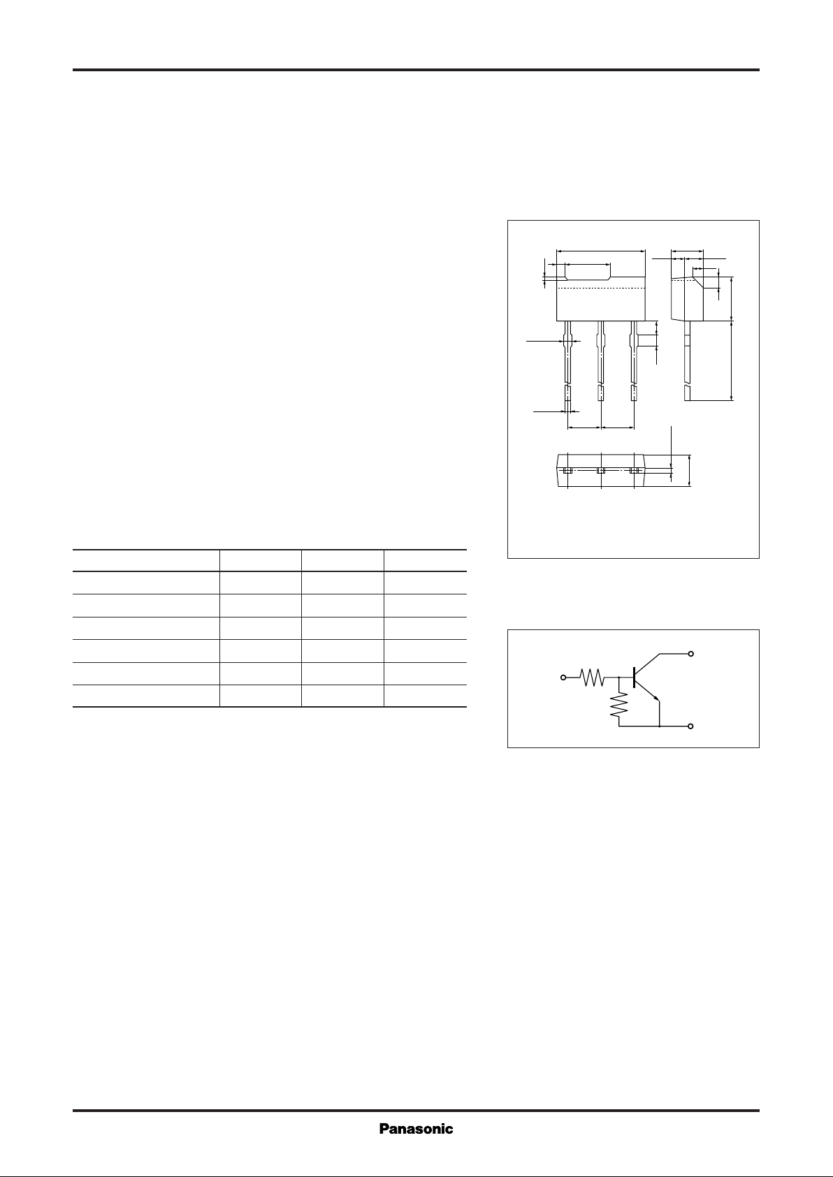
0.15
0.65 max.
0.7 4.0
6.9±0.1
1.05
±0.05
1.0
2.5±0.1
Unit: mm
(1.45)
0.8
0.8
3.5±0.114.5±0.5
Resistance by Part Number
■
(R1)(R
●
UN6221 2.2kΩ 2.2kΩ
●
UN6222 4.7kΩ 4.7kΩ
●
UN6223 10kΩ 10kΩ
●
UN6224 2.2kΩ 10kΩ
Absolute Maximum Ratings (Ta=25˚C)
■
Parameter Symbol Ratings Unit
Collector to base voltage V
Collector to emitter voltage
Collector current I
Total power dissipation P
Junction temperature T
Storage temperature T
CBO
V
CEO
C
T
j
stg
)
2
50 V
50 V
500 mA
600 mW
150 ˚C
–55 to +150 ˚C
+0.1
0.45
–0.05
2.5±0.5 2.5±0.5
123
Internal Connection
0.85
–0.05
+0.1
0.45
2.5±0.1
1 : Emitter
2 : Collector
3 : Base
MT -1 Type Pakage
1
Transistors with built-in Resistor UN6221/6222/6223/6224
Electrical Characteristics (Ta=25˚C)
■
Parameter Symbol Conditions min typ max Unit
Collector cutoff current
Emitter
cutoff
current
UN6221 5
UN6222 I
UN6223/6224 1
Collector to base voltage V
Collector to emitter voltage V
Forward
current
transfer
ratio
UN6221 40
UN6222 h
UN6223/6224 60
Collector to emitter saturation voltage V
Output voltage high level V
Output voltage low level V
Transition frequency f
Input
resistance
UN6221/6224 2.2
UN6222 R
UN6223 10
Resistance ratio
UN6224 0.17 0.22 0.27
I
CBO
I
CEO
EBO
CBO
CEO
FE
CE(sat)
OH
OL
T
1
R1/R
VCB = 50V, IE = 0 1 µA
VCE = 50V, IB = 0 1 µA
VEB = 6V, IC = 0 2 mA
IC = 10µA, IE = 0 50 V
IC = 2mA, IB = 0 50 V
VCE = 10V, IC = 100mA 50
IC = 100mA, IB = 5mA 0.25 V
VCC = 5V, VB = 0.5V, RL = 500Ω 4.9 V
VCC = 5V, VB = 3.5V, RL = 500Ω 0.2 V
VCB = 10V, IE = –50mA, f = 200MHz
200 MHz
(–30%) 4.7 (+30%) kΩ
0.8 1.0 1.2
2
2
 Loading...