

Panasonic UNR1231A, UNR1231 Datasheet
Transistors with built-in Resistor
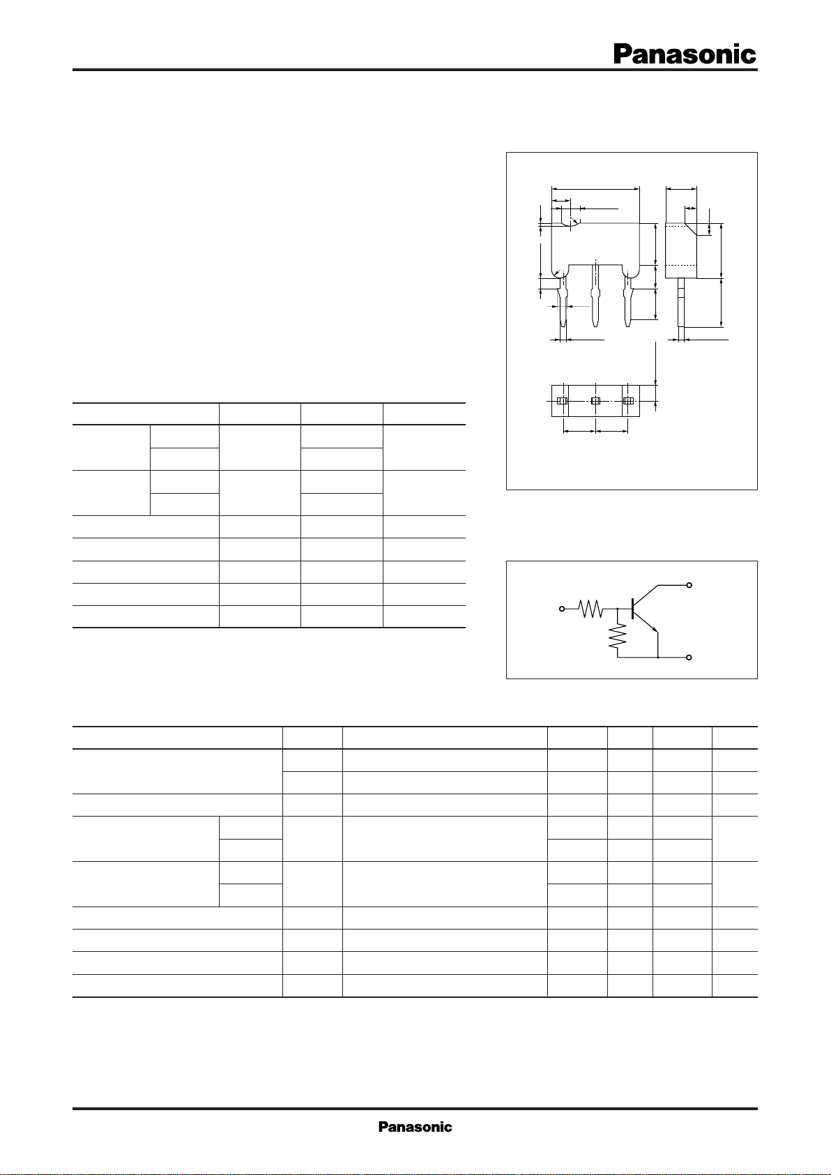
B
C
R1(1kΩ
)
R2
(
47kΩ
)
E
UN1231/1231A
Silicon NPN epitaxial planer transistor
For amplification of the low frequency
Features
■
●
High forward current transfer ratio hFE.
●
M type mold package.
●
Costs can be reduced through downsizing of the equipment and
reduction of the number of parts.
6.9±0.1
1.5
0.4
1.0±0.1
1.5 R0.9
R0.9
R0.7
0.85
0.55±0.1 0.45±0.05
3.5±0.1
2.0±0.2
2.4±0.21.25±0.05
Unit: mm
2.5±0.1
1.0
1.0
4.1±0.2 4.5±0.1
Absolute Maximum Ratings (Ta=25˚C)
■
Parameter Symbol Ratings Unit
Collector to
base voltage
Collector to
emitter voltage
UN1231
UN1231A 60
UN1231
UN1231A 50
Collector current I
Peak collector current I
V
CBO
V
CEO
C
CP
20
V
20
V
0.7 A
1.5 A
Total power dissipation PT* 1.0 W
Junction temperature T
Storage temperature T
j
stg
150 ˚C
–55 to +150 ˚C
* Printed circuit board: Copper foil area of 1cm2 or more and thickness of
1.7mm for the collector portion.
Electrical Characteristics (Ta=25˚C)
■
Parameter Symbol Conditions min typ max Unit
Collector cutoff current
Emitter cutoff current I
I
I
CBO
CEO
EBO
VCB = 15V, IE = 0 1 µA
VCE = 15V, IB = 0 10 µA
VEB = 14V, IC = 0 0.5 mA
UN1231
Collector to base voltage
UN1231A
V
CBO
IC = 10µA, IE = 0
UN1231
Collector to emitter voltage
UN1231A
Forward current transfer ratio h
Collector to emitter saturation voltage V
Input resistance R
Resistance ratio R1/R
V
FE
CEO
CE(sat)
1
2
IC = 1mA, IB = 0
VCE = 10V, IC = 150mA* 800 2100
IC = 100mA, IB = 5mA* 0.4 V
2.5 2.5
Internal Connection
20
60
20
50
0.7 1 1.3 kΩ
0.021
123
1:Base
2:Collector
3:Emitter
M Type Mold Package
V
V
*Pulse measurement
1
Transistors with built-in Resistor
UN1231/1231A
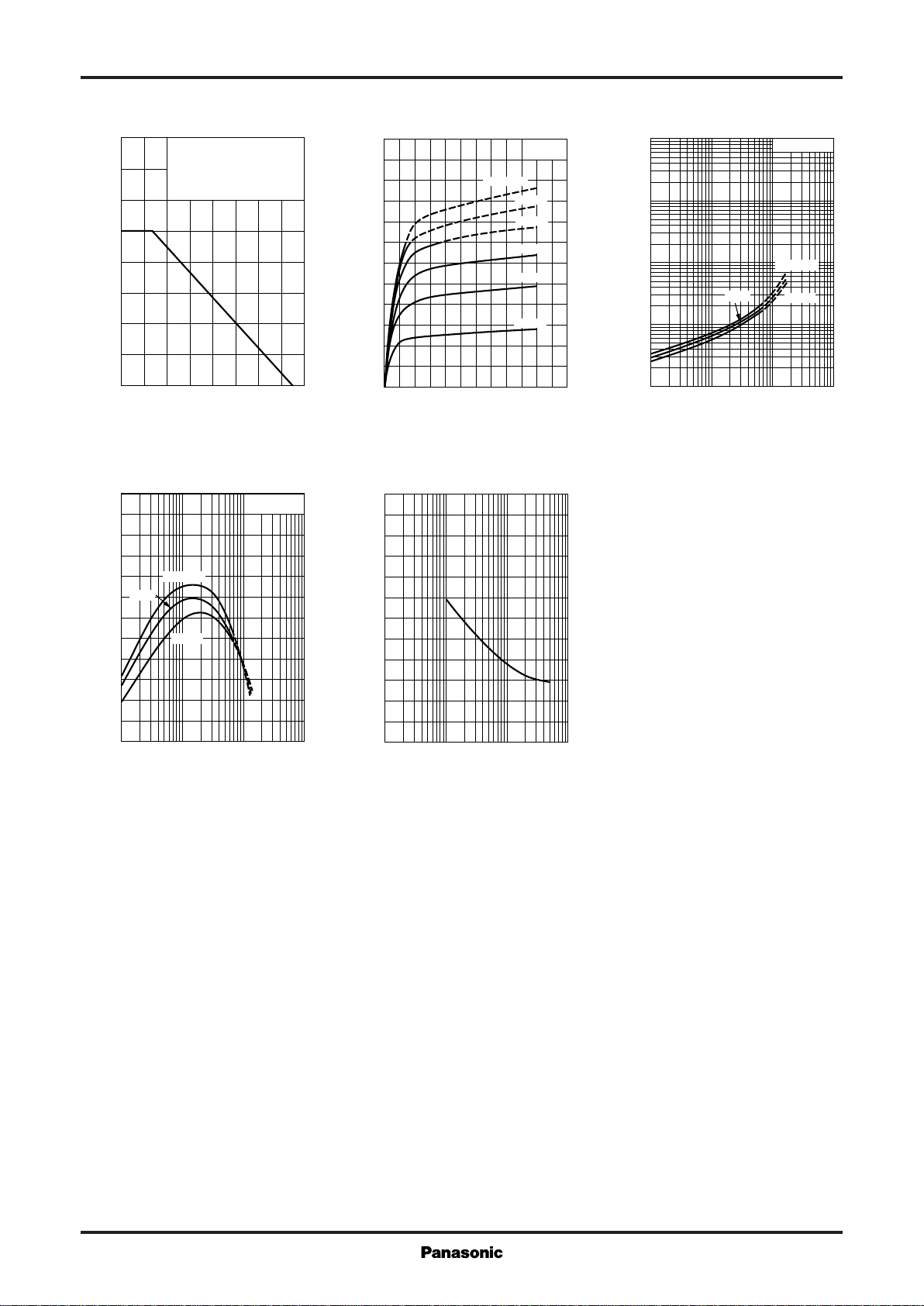
PT — Ta IC — V
1.6
1.4
)
W
(
1.2
T
1.0
0.8
0.6
0.4
Total power dissipation P
0.2
0
0 16040 12080
Ambient temperature Ta (˚C
Copper foil area of 1cm2 or
more and thickness of
1.7mm for the collector
portion.
hFE — I
2400
FE
2000
C
VCE=10V
V
CE(sat)
— I
25˚C
C
IC/IB=100
Ta=75˚C
–25˚C
1.2
1.0
)
A
(
0.8
C
0.6
0.4
Collector current I
0.2
CE
IB=1.2mA
Ta=25˚C
1.0mA
0.8mA
0.6mA
0.4mA
0.2mA
100
)
V
(
30
CE(sat)
10
0.3
0.1
0.03
3
1
Collector to emitter saturation voltage V
0
012210486
)
Collector to emitter voltage VCE (V
Cob — V
30
CB
)
0.01
0.01 0.03
Collector current IC (A
0.1 0.3 1 3 10
)
)
pF
(
25
ob
1600
1200
800
400
Forward current transfer ratio h
0
0.01 0.03
Ta=75˚C
25˚C
–25˚C
0.1 0.3 1 3 10
Collector current IC (A
20
15
10
5
Collector output capacitance C
0
0.1 0.3
)
Collector to base voltage VCB (V
1 3 10 30 100
)
2
 Loading...