

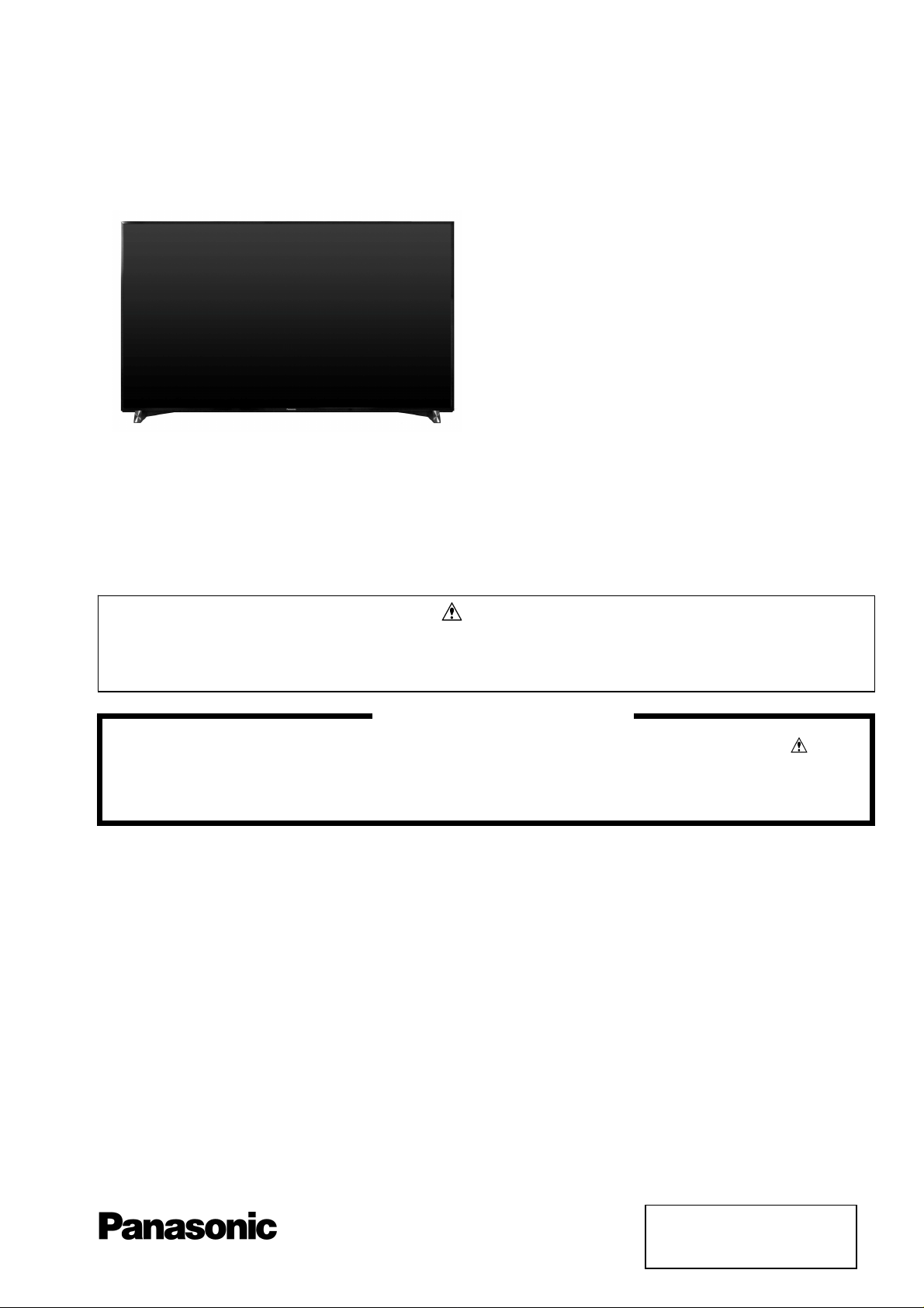
Panasonic TX-65DX902B Schematic
ORDER No. PCZ1602005CE
Service Manual
LED TV
TX-65DX902B
LA65 Chassis
This service information is designed for experienced repair technicians only and is not designed for use by the general public. It does not
contain warnings or cautions to advise non-technical individuals of potencial dangers in attempting to service a product. Products
powered by electricity should be serviced or repaired only by experienced professional technicians. Any attempt to service or repair the
product or products deal within this service information by anyone else could result in serious injury or death.
There are special components used in this equipment which are important for safety. These parts are marked in the
Schematic Diagrams, Circuit Board Diagrams, Explorer Views and Replacement Parts List. It is essential that these
critical parts should be replaced with manufacturer´s specified parts to prevent shock, fire or other hazards. Do not
modify the original design without permission of manufacturer.
IMPORTANT SAFETY NOTICE
Warning
© Panasonic Corporation 2016.
Unauthorized copying
distribution is a violation of law.
and

CONTENTS
2
SAFETY PRECAUTIONS ........................................... 3
GENERAL GUIDE LINES ...................................... 3
TOUCH – CURRENT CHECK ............................... 3
PREVENTION OF ELECTROSTATIC DISCHARGE
(ESD) TO ELECTROSTATICALLY SENSITIVE (ES)
DEVICES .................................................................... 4
ABOUT LEAD FREE SOLDER (PBF) ......................... 5
SUGGESTED PB FREE SOLDER ........................ 5
SERVICE NAVIGATION ............................................. 6
CHASSIS BOARD LAYOUT .................................. 6
SERVICE HINTS ........................................................ 7
APPLICABLE SIGNALS .............................................. 8
SPECIFICATIONS ...................................................... 9
TECHNICAL DESCRIPTION ................................ ….11
SPECIFICATION OF KEY FOR DTCP-IP,
C2MOD, CI PLUS, DIMORA, HDCP2.2,
NETFLIX, WIDEVINE, FREETIME ....................... 11
GENERAL INFORMATION ................................. 11
REPLACEMENT OF ICS ..................................... 11
MODEL AND KEYS ............................................ 11
USB HDD RECORDING ..................................... 11
SETTING INSPECTION ............................................ 12
CS MAINTENANCE MENU ...................................... 13
SYSTEM INFORMATION ......................................... 15
HOTEL MODE .......................................................... 16
DATA COPY BY USB MEMORY .............................. 17
DATA COPY FROM TV SET TO USB MEMORY ..... 18
DATA COPY FROM USB MEMORY TO TV SET ..... 19
OPTION BYTES DESCRIPTION .............................. 20
SELF CHECK ........................................................... 21
POWER LED BLINKING TIMING CHART ................ 22
LCD PANEL TEST MODE ........................................ 22
WIRING DIAGRAM ................................................... 23
BLOCK DIAGRAM (1 OF 3) ...................................... 24
PARTS LOCATION ................................................... 27
LOCATION OF LEAD WIRING ................................. 30
LOCATION OF FAN UNITS ...................................... 31
LOCATION OF HEAT RUBBERS ............................. 32
LOCATION OF GASKETS ........................................ 33
LOCATION OF FELTS ON LCD PANEL AND SP
BRACKETS ............................................................... 34
PACKING TRUCTURE ............................................. 35
REPLACEMENT PARTS LIST NOTE ....................... 36
REPLACEMENT PARTS LIST .................................. 37
SCHEMATIC DIAGRAMS NOTE .............................. 81
A-BOARD (1 OF 27) SCHEMATIC DIAGRAM .......... 82
P-BOARD (1 OF 2) SCHEMATIC DIAGRAM .......... 109
PB-BOARD (1 OF 2) SCHEMATIC DIAGRAM ....... 111
K-BOARD SCHEMATIC DIAGRAM ........................ 113
GK-BOARD SCHEMATIC DIAGRAM ..................... 114
CONDUCTOR VIEWS ............................................ 115
Safety Precautions
3
General Guide Lines
1. When servicing, observe the original lead dress. If a short circuit is found, replace all parts which have been overheated
or damaged by the short circuit.
2. After servicing, see to it that all the protective devices such as insulation barriers, insulation papers shields are properly
installed.
3. After servicing, make the following touch current checks to prevent the customer from being exposed to shock hazards.
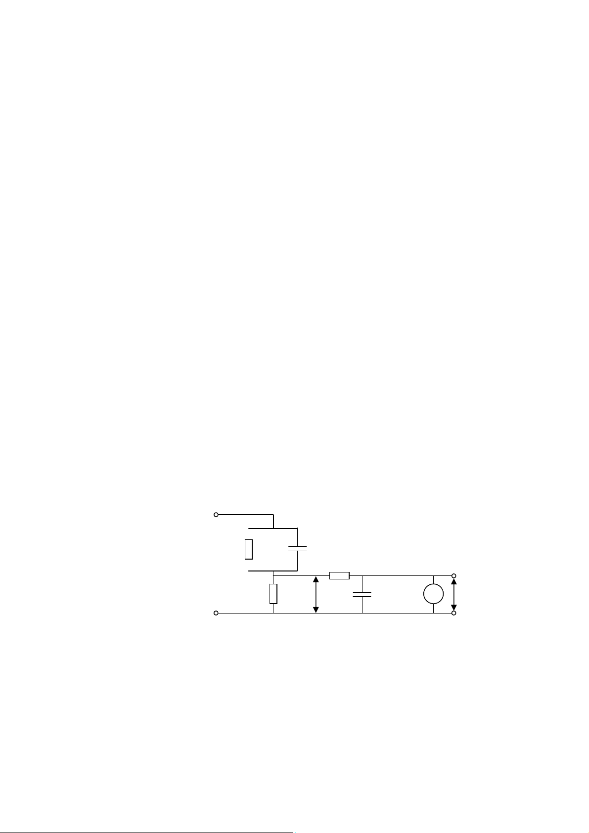
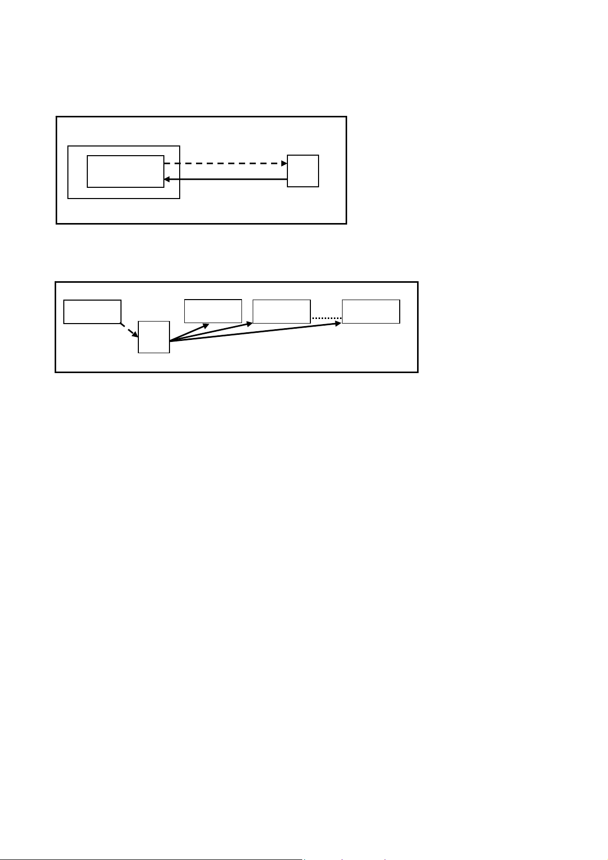
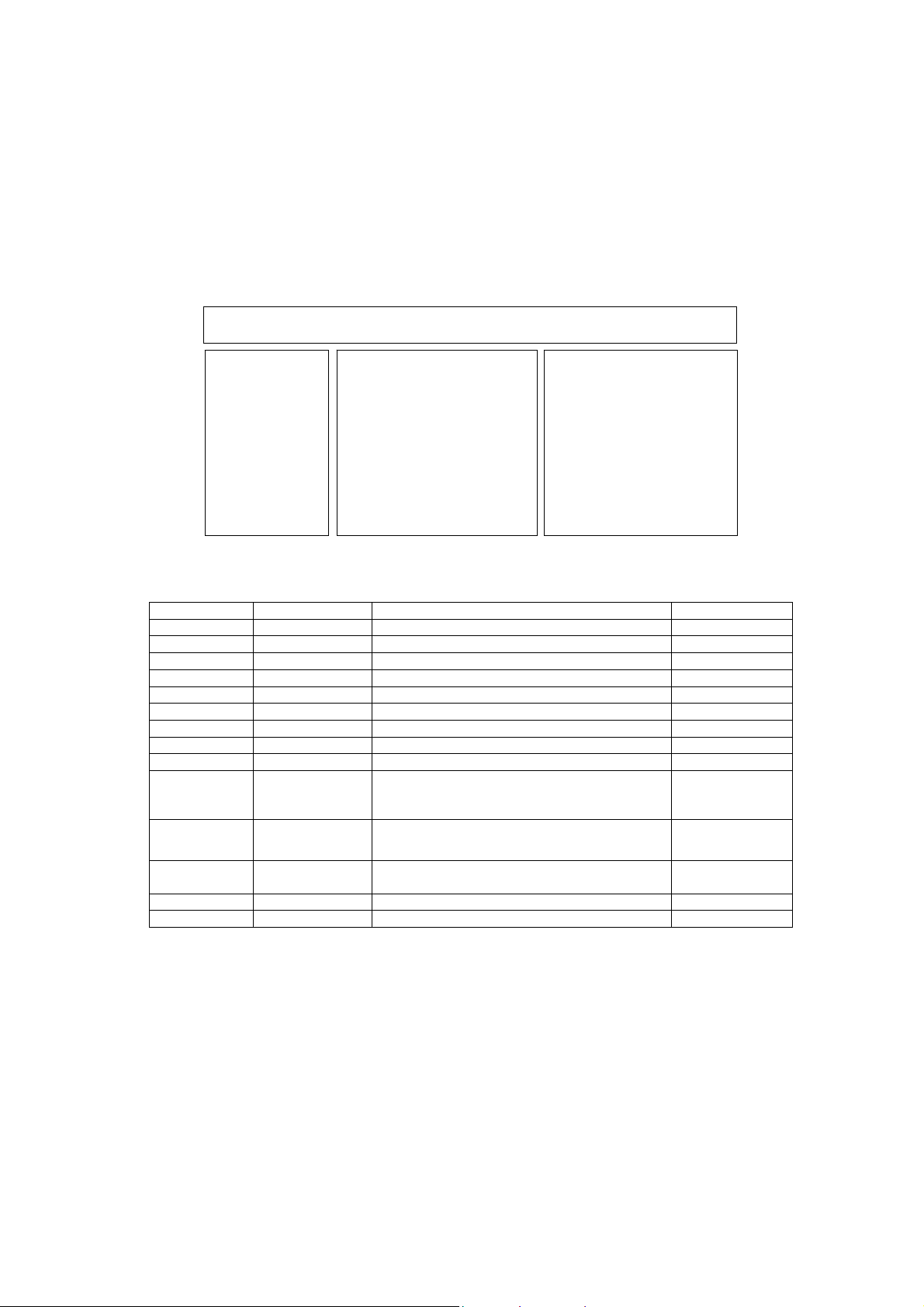
Touch-Current Check
1. Plug the AC cord directly into the AC outlet. Do not use an isolation transformer for this check.
2. Connect a measuring network for touch currents between each exposed metallic part on the set and a good earth
ground such as a water pipe, as shown in Fig. 1.
3. Use Leakage Current Tester (Simpson 228 or equivalent) to measure the potential acr oss the measuring network.
4. Check each exposed metallic part, and measure the voltage at each point.
5. Reserve the AC plug in the AC outlet and repeat each of the above measure.
6. The potential at any point (TOUCH CURRENT) expressed as voltage U1 and U2, does not exceed the following values:
For a. c.: U1 = 35 V (peak) and U2 = 0.35 V (peak);
For d. c.: U1 = 1.0 V,
Note:
The limit value of U2 = 0.35 V (peak) for a. c. and U1 = 1.0 V for d. c. correspond to the values 0.7 mA (peak) a. c. and
2.0 mA d. c.
The limit value U1 = 35 V (peak) for a. c. correspond to the value 70 mA (peak) a. c. for frequencies greater than 100
kHz.
7. In case a measurement is out of the limits specified, there is a possibility of a shock hazard, and the equipment shoul d
be repaired and rechecked before it is returned to the customer.
COLD
WATER PIPE
(EARTH GROUND)
TO
APPLIANCES
EXPOSED
METAL PARTS
Resistance values in ohms ()
V: Voltmeter or oscilloscope
(r.m.s. or peak reading)
Measuring network for TOUCH CURRENTS
=0.22F
Fig. 1
C
S
10k
(V)
U
1
=1500
R
S
R0=500
Input resistance: 1M
Input capacitance:200pF
Frequency range: 15Hz to 1MHz and d.c.respectively
0.022
F
V
U2 (V)

Prevention of Electrostatic Discharge (ESD) to Electrostatically
4
Sensitive (ES) Devices
Some semiconductor (solid state) devices can be damaged easily by static electricity. Such components commonly are
called Electrostatically Sensitive (ES) Devices. Examples of typical ES devices are integrated circuits and some field-effect
transistors and semiconductor "chip" components. The following techniques should be used to help reduce the incidence of
component damage caused by electrostatic discharge (ESD).
1. Immediately before handling any semiconductor component or semiconductor-equipped assembly, drain off any ESD on
your body by touching a known earth ground. Alternatively, obtain and wear a commercially available discharging ESD
wrist strap, which should be removed for potential shock reasons prior to applying power to the unit under test.
2. After removing an electrical assembly equipped with ES devices, place the assembly on a conductive surface such as
aluminum foil, to prevent electrostatic charge build up or exposure of the assembly.
3. Use only a grounded-tip soldering iron to solder or unsolder ES devices.
4. Use only an anti-static solder removal device. Some solder removal devices not classified as "anti-static (ESD
protected)" can generate electrical charge sufficient to damage ES devices.
5. Do not use freon-propelled chemicals. These can generate electrical charges sufficient to damage ES devices.
6. Do not remove a replacement ES device from its protective package until immediately before you are ready to install it.
(Most replacement ES devices are packaged with leads electrically shorted together by cond uctive foam, aluminum foil
or comparable conductive material).
7. Immediately before removing the protective material from the leads of a replacement ES device, touch the protective
material to the chassis or circuit assembly into which the device will be installed.
Caution
Be sure no power is applied to the chassis or circuit, and observe all other safety precautions.
8. Minimize bodily motions when handling unpackaged replacement ES devices. (Otherwise harmless motion such as th e
brushing together of your clothes fabric or the lifting of your foot from a carpeted floor can generate static electricity
(ESD) sufficient to damage an ES device).
There are special components used in this equipment which are important for safety.
These parts are marked by in schematic diagrams, exploded views and replacement parts list. It is essential that
these critical parts should be replaced with manufacturer’s specified parts to prevent shock, fire, or other hazards. Do
not modify the original design without permission of manufacturer.
IMPORTANT SAFETY NOTICE
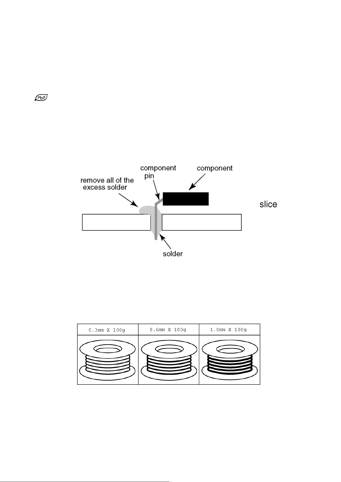
About lead free solder (PbF)
5
Note: Lead is listed as (Pb) in the periodic table of elements.
In the information below, Pb will refer to Lead solder, and PbF will refer to Lead Free Solder.
The Lead Free Solder used in our manufacturing process and discussed below is (Sn+Ag+Cu).
That is Tin (Sn), Silver (Ag) and Copper (Cu) although other types are available.
This model uses Pb Free solder in it’s manufacture due to environmental conservation issues. For service and repair work,
we’d suggest the use of Pb free solder as well, although Pb solder may be used.
PCBs manufactured using lead free solder will have the PbF within a leaf Symbol
stamped on the back of PCB.
Caution
Pb free solder has a higher melting point than standard solder. Typically the melting point is 50 ~ 70 °F (30~40°C)
higher. Please use a high temperature soldering iron and set it to 700 ± 20 °F (370 ± 10 °C).
Pb free solder will tend to splash when heated too high (about 1100 °F or 600 °C).
If you must use Pb solder, please completely remove all of the Pb free solder on the pins or solder area before
applying Pb solder. If this is not practical, be sure to heat the Pb free solder until it melts, before applying Pb solder.
After applying PbF solder to double layered boards, please check the component side for excess solder which may
flow onto the opposite side. (see Fig.2)
Suggested Pb free solder
There are several kinds of Pb free solder available for purchase. This product uses Sn+Ag+Cu (tin, silver, copper) solder.
However, Sn+Cu (tin, copper), Sn+Zn+Bi (tin, zinc, bismuth) solder can also be used. (see Fig.3)
Fig.2
Fig.3
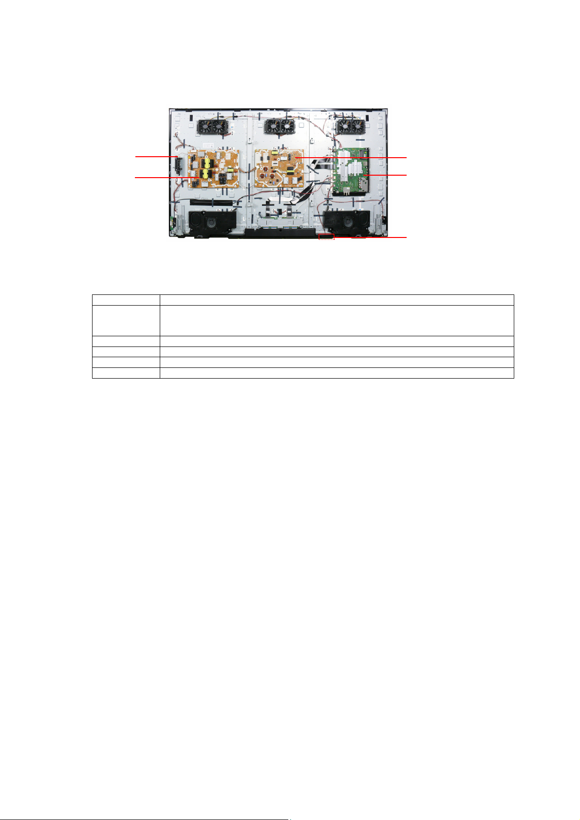
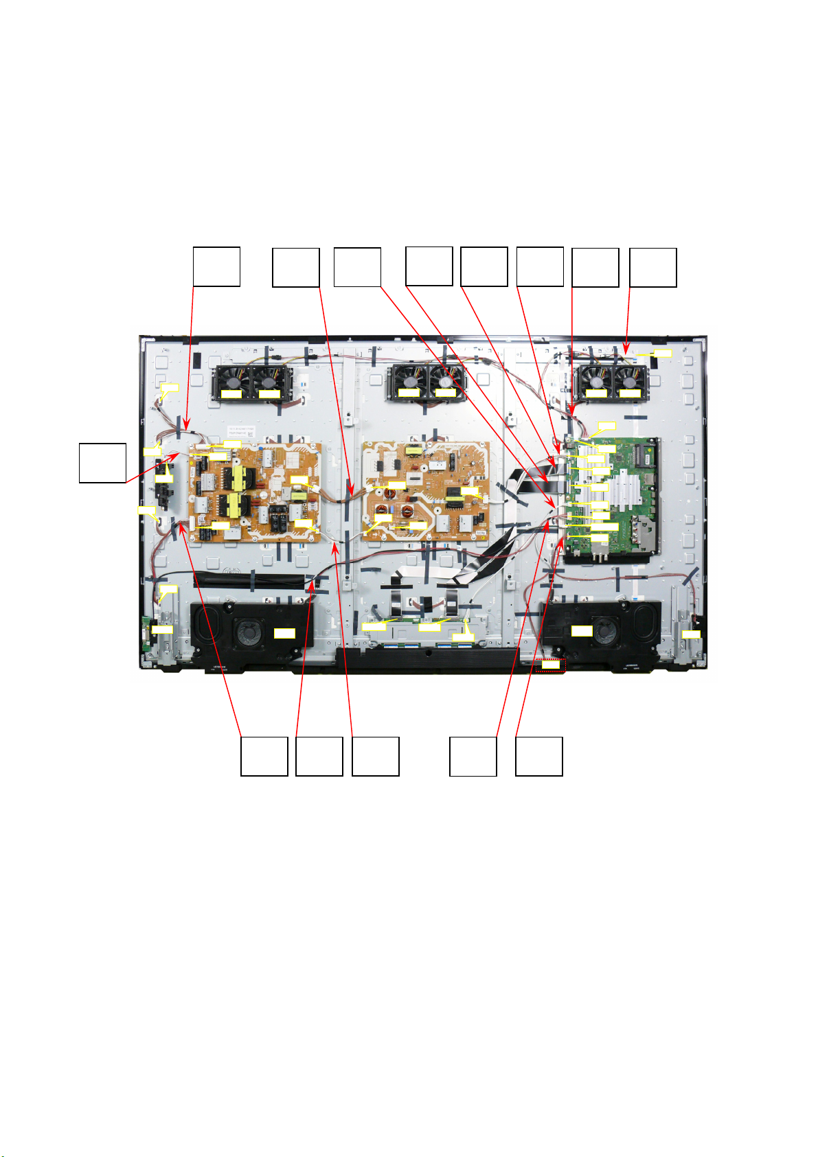
Service Navigation
6
Chassis Board Layout
GK-BOARD
PB-BOARD
Board Name Function
A-Board AV Terminal, HDMI, USB, WIFI, BT, Ethernet, Digital Audio Out, SD Slot,
CI Slot , DUAL TUNER A/DVB-T/T2/C/S , DVB-T2/T/C/S2/S Dem, Peaks IC_MTK,
Speaker out, Woofer out, HP, eMMc Memory, DDR SDRAM, FRC(NTK), GCEX2
P-Board Main Input, Power Supply
PB-Board Power Supply (DC-DC)
K-Board Remote Receiver, Power and Timer LED, C.A.T.S
GK-Board Key control, Power switch
P-BOARD
A-BOARD
K-BOARD
Note:
P/PB –BOARD - Do not touch at HOT circuit due to high voltage
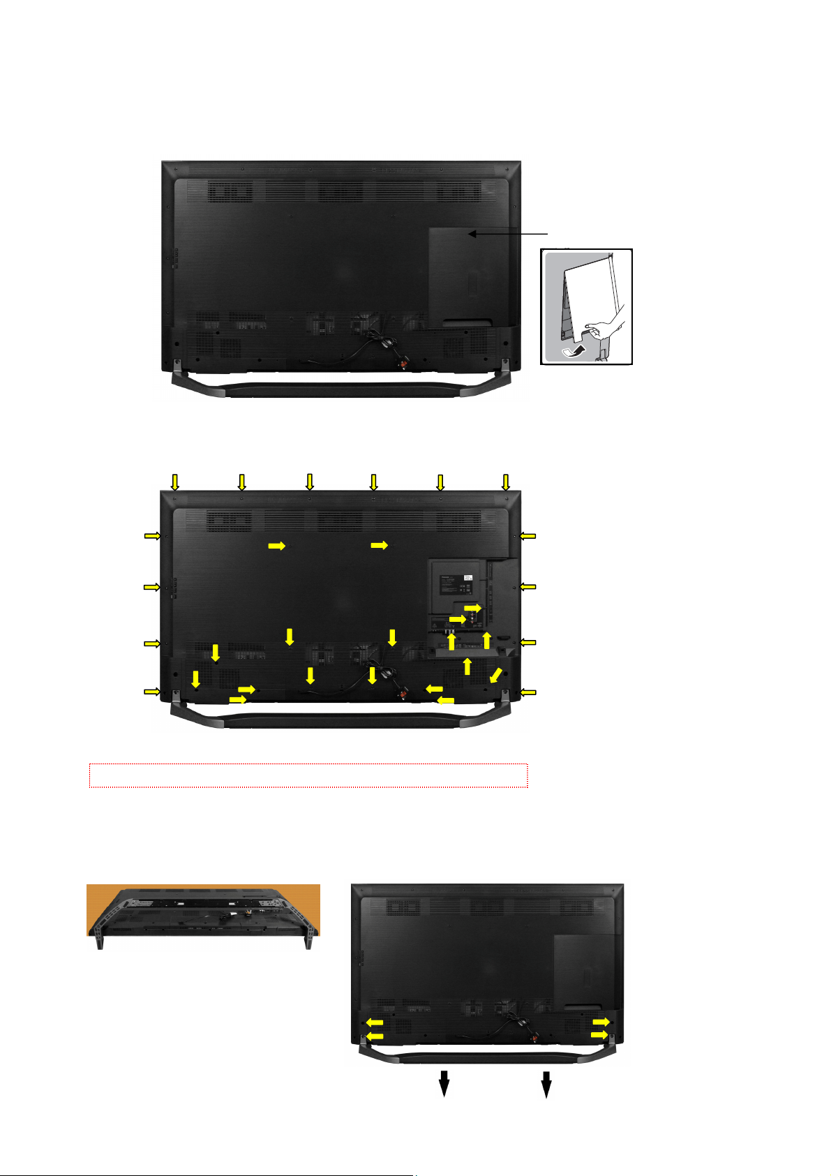
Service Hints
7
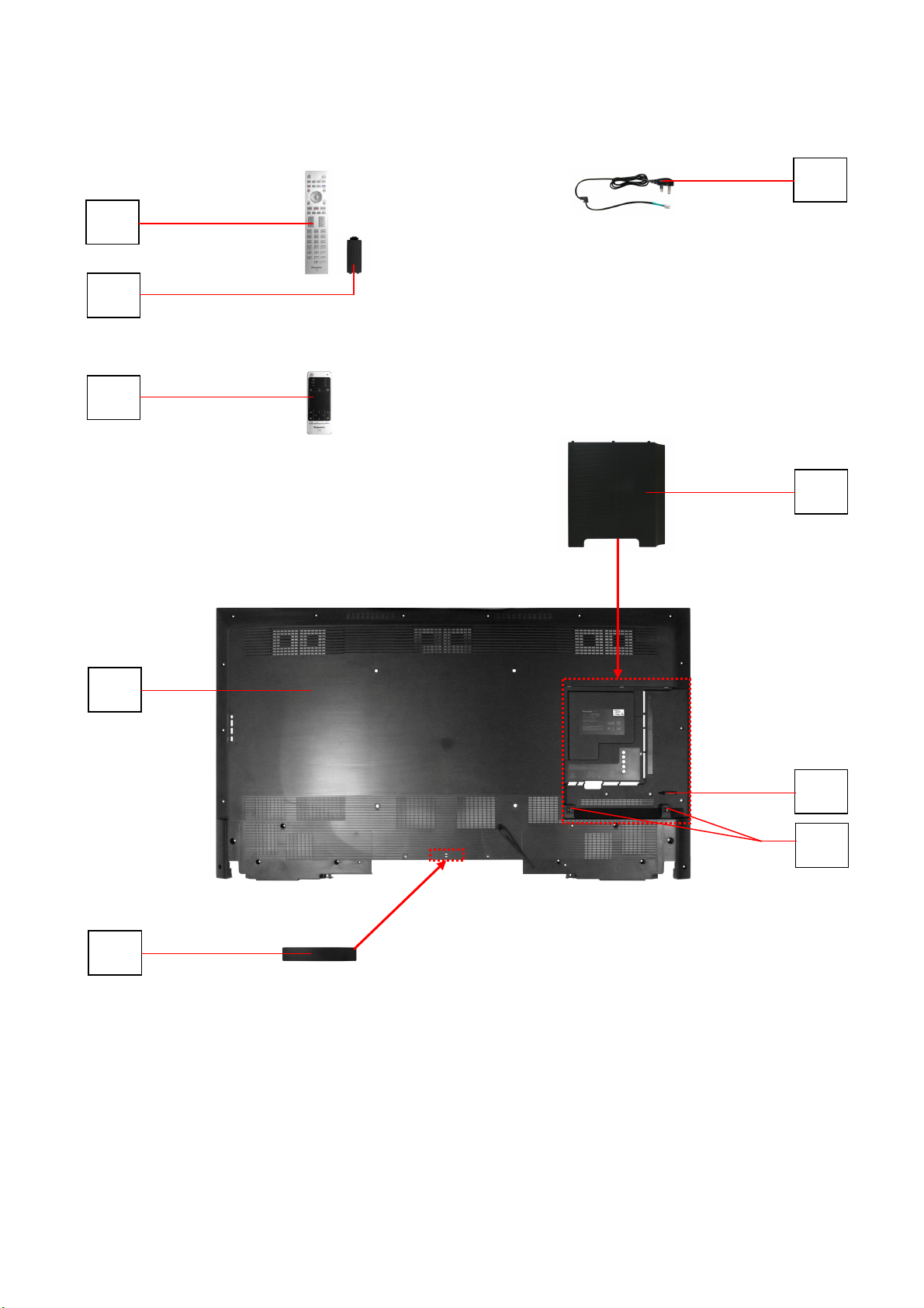
How to remove the backcover
Remove the Cable Cover. (see Fig.4)
Remove the 32 fixing screws and the back cover.(see Fig.5)
(1)
(1)
(1)
(1)
(2)
(2)
(1)
(1)
(3)
(3)
(2)
(1)
(2)
Fig.4
(1)
(3)
(3)
(2)
(1)
(2)
(2)
(1)
(1)
(2)
(2)
(1)
Caution: Before removing cover, receiver must be disconnect from mains.
How to remove the pedestal assembly
Lay the main unit face down. (see Fig.6)
Remove the 4 fixing screws and the pedestal assembly. (see Fig.7)
Fig.5
Fig.6
Cable Cover
(1) (1)
SCREWS
(1) THEC2489 /18pcs/
(2) THTD037J /10pcs/
(3) THE5ZC036J /4pcs/
(1)
(1)
(1)
(2)
(1)
SCREWS
(4) THE5ZL002N /4pcs/
(4)
(4)
(4)
(4)
Fig.7

Applicable Signals
8
Component (Y, Pb, Pr) (from AV2 terminal), HDMI
525 (480) / 60i,60p * *
625 (576) / 50i, 50p * *
750 (720) / 60p, 50p * *
1,125 (1,080) / 60i, 50i * *
1,125 (1,080) / 60p, 50p, 24p *
3,840 x 2,160 / 60p, 50p, 30p, 25p, 24p *
4,096 x 2,160 / 60p, 50p, 30p, 25p, 24p *
Note:
Signal name COMPONENT HDMI
Signals other than above may not be displayed properly.
The above signals are reformatted for optimal viewing on your display.

Specifications
9
Power Source: 220-240V AC, 50 / 60Hz
Rated Power Consumption: 531W
Stand-by Power Consumption: 0.50W
Aerial Impedance: 75 unbalanced, Coaxial Type
Receiving System: TX-65DX902B (UK)
DVB-S/S2 Freesat services via Satellite dish input.
DVB-T/T2 Digital terrestrial services
PAL I UHF E21-E68
PAL 525/60 (AV only)
M.NTSC (AV only)
NTSC (AV only)
TX-65DX902B (Ireland)
DVB-S/S2 Receiver frequency range – 950 MHz to 2,150MHz.
DVB-T/T2 Digital terrestrial services
PAL I VHF A-J
UHF E21-E69
CATV S1-S20
CATV S21-S41(Hyperband)
PAL 525/60 (AV only)
M.NTSC (AV only)
NTSC (AV only)
Satellite dish input: Female F-type 75 x 2
Aerial - Rear:
UHF VHF/UHF
Operating Conditions: Temperature: 0°C 35°C
TX-65DX902B (UK) TX-65DX902B (Ireland)
Humidity: 20% 80% RH (non condensing)
Terminals:
AV IN (COMPONENT/VIDEO)
VIDEO Video (RCAx1) 1V p-p 75
Video (RCAx3) Y:1V p-p 75 (including synchronisation)
Pb/Cb, Pr/Cr: ±0.35V p-p 75
AUDIO IN Audio (RCAx2) 500mV rms 10k (used for HDMI analogue audio IN)
HDMI1/2/3/4 Type A Connectors
HDMI
Deep Colour, x.v.Colour
HDMI 2 : 4K, 3D (3D content of 4K format is not supported), Content Type,
Audio Return Channel, Deep Colour, x.v.Colour
This TV supports “HDAVI Control 5” function.
DIGITAL AUDIO OUT PCM / Dolby digital, Fibre optic
USB 1/2/3 USB1/2 :DC 5V, Max 500mA [Hi-Speed USB (USB 2.0)]
USB3 :DC 5V, Max 900mA [SuperSpeed USB (USB 3.0)]
ETHERNET RJ45, IEEE802.3 10BASE-T / 100BASE-TX
CARD SLOT SD Card slot x 1
Common interface slot (Complies with CI+) x 1
Wireless LAN:
Standard Compliance IEEE802.11a/n , IEEE802.11b/g/n
Frequency Range IEEE802.11a/n: 5.180 GHz – 5.320 GHz
5.500 GHz – 5.580 GHz
5.660 GHz – 5.700 GHz
IEEE802.11b/g/n: 2.412 GHz – 2.472 GHz
Security WPA2-PSK (TKIP/AES)
WPA-PSK (TKIP/AES)
WEP(64 bit/128 bit)
(Freesat / Other Sat.) Receiver frequency range – 950 MHz to 2,150MHz.
Not available for DISEqC control.
Not available for DISEqC control.
1/3/4 : 4K, 3D (3D content of 4K format is not supported), Content Type,
TM
TM

Bluetooth wirelless
10
technology:
Standard Compliance Bluetooth 3.0
Frequency Range 2.402 GHz – 2.480 GHz
LED LCD screen: TZLP174WYVE
3840 x 2160, 16:9
Visible Diagonal 1640mm
Audio Output: 40W (2 x10W + 2 x10W)
Headphones: 3.5mm, 8 Impedance
Accessories supplied : Remote Control
Touch Pad Remote Control
Cable guide
4 x R03 Batteries
Dimensions:
Width: Height: Depth:
Including TV stand 1,457mm 888mm 334mm
TV set only 1,457mm 844mm 64mm
Mass:
Including TV stand 42.5kg
TV set only 34.5kg
Design and Specifications are subject to change without notice.
Mass and dimensions shown are approximate.

Technical Description
11
Specification of KEY for DTCP-IP, C2MOD, CI Plus, DIMORA, HDCP2.2, Netflix,
Widevine, Freetime
General information:
1. eMMc Memory(IC8920) for spare parts has the seed of KEY for each.
2. The final KEY data will be generated by MTK IC (IC8000) when SELF CHECK was done and are stored in both
MTK IC (IC8000) and eMMc (IC8920).
All KEYs are not generated for all models.
The necessary KEY are only generated and stored depend on the feature of models.
Replacement of ICs:
When MTK IC (IC8000) is replaced, eMMc (IC8920) should be also replaced with new one the same time.
When eMMc Memory(IC8920) is replaced, MTK IC (IC8000) is not necessary to be replaced the same time.
After the replacement of IC, SELF CHECK should be done to generate the final KEY data.
How to SELF CHECK: While pressing [VOLUME ( - )] button on the main unit, press the MENU button on the remote
control for more than 3 seconds.
TV will be forced to the factory shipment setting after this SELF CHECK.
Model and Keys:
Keys
Model No.
TX-65DX902B Yes Yes Yes Yes Yes Yes Yes
DTCP-IP C2MOD CI PLUS DIMORA HDCP2.2
Netflix
Widevine
MAC
FREETIME
USB HDD Recording:
General information:
Digital TV programmes can be recorded in USB HDD.
C2MOD key generated in A-board by SELF CHECK binds TV and USB-HDD for communication.
That key is only one key for them. If the key is different, TV can not access USB-HDD.
Caution:
New key will be generated by following SELF CHECK and previous TV programmes recorde d in USB HDD will not be
viewed.
SELF CHECK: While pressing [VOLUME ( - )] button on the main unit, press the MENU button on the remote control for more
then 3 seconds.

Setting Inspection
V
V
V
V
V
12
Voltage Confirmation
A board
Description Test point
PNL12V TP4059 12V ± 1.2V
USB5V TP5221 5.18V ± 0.25V
USB1 TP8701 5.00V ± 0.25V
USB2 TP8705 5.00V ± 0.25V
USB3 TP8711 5.00V ± 0.25V
USB-WiFi TP8718 5.14V ± 0.20V
USB-4KDEMO TP8724 5.14V ± 0.20V****
SUB3.3V TP5201 3.33V ± 0.15V
HDMI1.1V TP4503 1.13V ± 0.06V
HDMISW3.3V TP4514 3.35V ± 0.17V
SUB_AI_3.3V TP2206 3.30V ± 0.17V
STB_1.5V TP8101 1.52V ± 0.07V
SUB1.0V TP8100 1.02V ± 0.05V
AVDD1.0V TP8102 1.06V ± 0.05V
NT2.5V TP9170 2.52V ± 0.12V
NT1.5V TP9160 1.52V ± 0.07V
NT1.1V TP9150 1.13V ± 0.06V
GE_1.1V TP4450 1.10V – 1.19V
WOL3.3V/PHY3.3V TP8606 3.30V ± 0.17V
EU_TU_1.8V TP5704 1.84V ± 0.10V
LNB_PWR1 TP6702 18V ± 1.0V
LNB_PWR2 TP6703 18V ± 1.0V
SUB9V TP5004 9.0V ± 0.4V
T2_1.1V TP5705 1.15V ± 0.11V
SD3.3V TP8644 3.34V ± 0.17V
SUB_CI_5V TP6406 5.0V ± 0.5V
P board
Description Test point
16V TP7410/11/12 and GND TP7247/31
5VS TP7405/20 an d GND TP7247/31 5.25V ± 0.2V 5.25V ± 0.2V
PFC TP7201/02 and GND TP7203/04*** <340V 390V ± 15V
CF7101 “hot area” -- <50mV
PB board
Description Test point
PFC2 TP7654/55
VLED1
VLED2
* Connect AC 230V to P1 connector of P-PCB (Main switch is OFF).
** Set main switch is ON.
*** Beware, for testing of PFC use the GND (TP7203) in Hot area of P board – risk of electric shock.
**** Only in Shop Mode.
Note:
P/PB –BOARD - Do not touch at HOT circuit due to high voltage
TP7560/61/62/63
oltage
oltage*
<1V
oltage*
<340V
<1V
TP7581/82
<1V
oltage**
16V ± 0.6V
oltage**
390V ± 15V
29.86V ± 1.5V
29.86V ± 1.5V
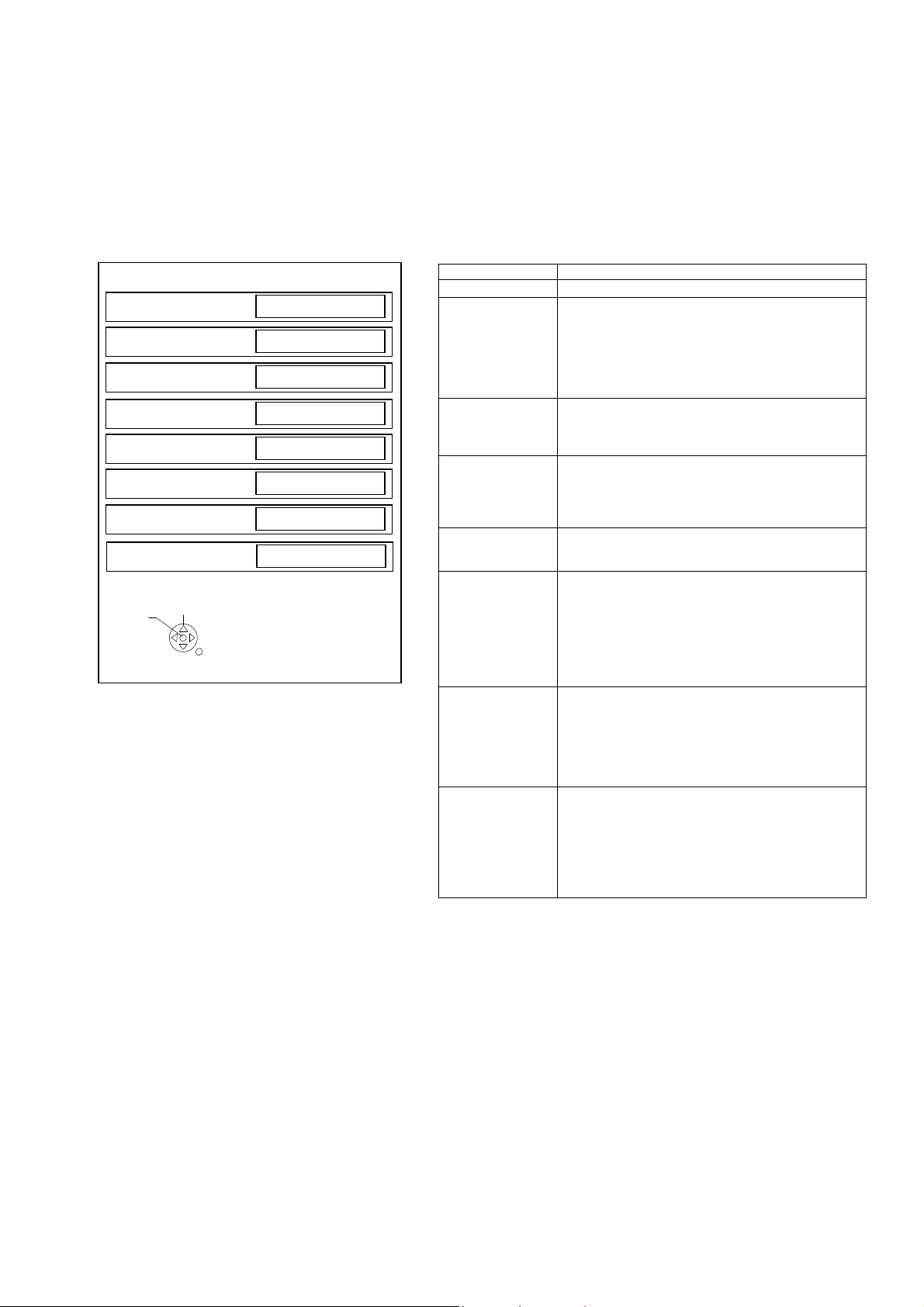
CS Maintenance Menu
13
MPU controls the functions switching for each IICs through IIC bus in this chassis. The following setting and adjustment can
be adjusted by remote control in Service Menu
How to enter into CS Maintenance Menu
Purpose
After exchange parts, check and adjust the contents of adjustment mode.
While pressing [VOLUME ( - )] button on the main unit, press the [RED] button on the remote control for 3 times within
2 seconds.
Note:
CS Maintenance Menu can not be entered when 3D signal input.
Input 2D signal to enter CS Maintenance Menu.
How to exit
Press the [EXIT] button on the remote control.
CS Maintenance Menu
OPT
EDID CLK
DRV CHECK
WB-ADJ
Key Command
Press the ( / / / ) button to step up/down/right/left through the functions and adjustments
Press the OK button to change the adjustment values.
Press the RETURN button for return to the main menu.
OPT
1.Select [OPT] in CS Maintenance Menu.
2.Press [OK] button or Cursor key [Right] on the remote control.
CS Maintenance Menu
OPT
EDID CLK
DRV CHECK
WB-ADJ
7 6 5 4 3 2 1 0
OPT1 0 0 0 0 0 1 0 0
OPT2 1 1 1 0 1 1 1 0
OPT3 0 0 0 0 0 0 0 1
OPT4 0 0 0 0 0 0 0 0
Exit:
Press the [EXIT] button or the [RETURN] button on the remote control.
EDID Clock
14
1.Select [EDID CLK] in CS Maintenance Menu.
2.Press [OK] button or Cursor key [Right] on the remote control.
CS Maintenance Menu
OPT
EDID CLK
DRV CHECK
EDID-CLK S-HIGH
HDMI 1
WB-ADJ
Exit:
Press the [EXIT] button or the [RETURN] button on the remote control.
DRV Check (USB HDD Drive Check)
1.Select [DRV CHECK] in CS Maintenance Menu.
2.Press [OK] button or Cursor key [Right] on the remote control.
CS Maintenance Menu
OPT ******** ***-**-OK
EDID CLK
DRV CHECK OK
ERROR-NG
******** ***-**-OK
WB-ADJ
Press [OK] button (3sec)
BUSY
Performing (Max 3minutes)
NG OK
OK NG
OK: HDD is normal
NG: HDD is failure or mismatch
USBHDD check History
******** *** -** OK…………This time :OK
ERROR-NG………………. Last time : NG
******** *** -** OK…………Before last time:OK
Exit:
Press the [EXIT] button or the [RETURN] button on the remote control.
WB-ADJ
1.Select [WB-ADJ] in CS Maintenance Menu.
2.Press [OK] button or Cursor key [Right] on the remote control.
CS Maintenance Menu
OPT
EDID CLK
DRV CHECK
WB-ADJ
Exit:
Press the [EXIT] button or the [RETURN] button on the remote control.
WB-ADJ
R-GAIN 5E
COLOR TEMP NORMAL
WB-ADJ
B-GAIN 67
COLOR TEMP NORMAL
COLOR TEMP:COOL
NORMAL
WARM
TUNING
Note:for change press [OPTION] button on Remote Control.
WB-ADJ
G-GAIN 80
COLOR TEMP NORMAL
Clock speed
HDMI Number

System Information
15
How to access
1. While pressing [MENU] button on the remote control.
2. To select [ Help] and then to select [System Information].(see Fig.8, Fig.9)
System Information
SW version 3002-10000-00d00-010006 3002
Status1 0d 0101-0003 0000-0800 0d
Status2 0012-100-0015fd 0012
Status3 00-000000-F000 00
Status4 A00024-0000019-00000 A
Status5 00000-10000 16e010ff 0
Status6 03006500-1000030 03006500
Status7 00000-0742 00000
HDAVI
Control
5 5 VIERA Link version is displayed
10000
00d00
010006
0101-0003
0000-0800
100
0015fd
00
00
00
F
00024
0000019
00000
0
0
0
0
1
0000
16e010ff
1000030
0742
How to exit
Press the [RETURN] button on the remote control.
*Sample only
Fig.9 Fig.8
Peaks SW
STBY SW
FRC SW
GCX SW
Outer model ID
Inner model ID
Panel inch size
LSI Package
LSI Release
Model data version
Number of bad block in NAND Flash (dec)
Peaks reboot counter
System crash counter
Emergency (SOS) counter
Peaks NAND Maker ID
Power-On period (A<=100hrs, B<=200hrs, C>200hrs)
Total Power-On time (dec, max is 65535)
Power-On timer (dec, max is 1048575)
Fixed (always)
SOS history (latest)
SOS history (last time)
SOS history (last but one)
SOS history (2
SOS history (1
Self-check _0-never selfcheck
1-production selfcheck by “FF” or USCM
2-user selfcheck by pressing “OK”
Fixed (always)
Panel ID
Peaks EEPROM version
STM EEPROM version
STM ROMCOR version
AJAX_CE version
nd
time after shipping)
st
time after shipping)
Hotel Mode
16
1. Purpose
Restrict a function for hotels.
2. Access command to the Hotel mode setup menu.
In order to display the Hotel mode setup menu,
please enter the following command (within 2 secon d).
[TV] : Vol.[Down] + [REMOTE] : AV (3 times)
Then, the Hotel mode setup menu is displayed.
Hotel mode
Hotel mode
Initial INPUT
Initial POS
Off
Off
Off
Initial VOL Level
Maximum VOL Level
Button Lock
Remote Lock
Off
100
Off
Off
Private Information
Change
Select
Keep
RETURN
3. To exit the “Hotel mode”:
Switch off the power with the [POWER] button
on the main unit or the [POWER] button
on the remote control or pressing [EXIT] button
on the remote control.
4. Explain the Hotel mode setup menu.
ITEM Function
Hotel Mode Select hotel mode ON/OFF
Initial INPUT Select input signal modes.
Initial POS Select programme number.
Initial VOL Level Adjust the volume when each time power is
Maximum VOL
Level
Button Lock Select local key conditions.
Remote Lock Select remote control key conditions.
Private
Information
Set the input, when each time power is switched on.
Selection:
Off/Freesat/DVB/AV/
HDMI1/HDMI2/HDMI3/HDMI4
*Off: give priority to the last memory. However, Euro
Model is compulsorily set to TV.
Selection:
Off/0 to 99
*Off: give priority to the last memory
switched on.
Selection/Range:
Off/0 to 100
*Off: give priority to the last memory
Adjust maximum volume.
Range:
0 to 100
Selection:
Off/SETUP/MENU
*Off: altogether valid
*Setup: only F-key is invalid
(Tuning guide (menu) can not be selected.)
*MENU: only F-key is invalid
(only Volume/Mute can be selected.)
Selected”
Off/SETUP/MENU/VOD
*Off: altogether valid
*Setup: only Setup menu is invalid
MENU: Picture/Sound/Setup menu are invalid
VOD:NETFLIX service is invalid
Select private information for VIERA Cast is Keep or
Reset if Hotel mode is set to [On] when TV power
on.
Selection :
Keep/Reset
•Keep: private information for VIERA Cast is keep
•Reset: private information for VIERA Cast is reset
Data Copy by USB Memory
17
Purpose
a) Board replacement (Copy the data when exchanging A-board):
When e xchanging A-board, the data in original A-board can be copied to USB Memory and then copy to new A-board.
TV
A-board
(Before exchanging)
Copy to USB Memory
(After exchanging)
Copy back from USB Memory
USB
Following data can be copied.
User setting data
(inc. Hotel mode setting data)
Channel scan data
Adjustment and factory preset data
b) Hotel (Copy the data when installing a number of units in hotel or any facility):
When insta lling a number of units in hotel or any facility, the data in master TV can be copied to USB Memory and the
copy to other TVs.
Master TV
Copy to USB Memory
USB
Memory
Other TV
Copy from USB Memory
Other TV
Other TV
Following data can be copied.
User setting data
(inc. Hotel mode setting data)
Channel scan data
Preparation
Make pwd file as startup file for (a) or (b) in an empty USB Memory.
1. Insert an empty USB Memory to your PC.
2. Right-click a blank area in a USB Memory window, point to New, and then click text document. A new file is created
by default (New Text Document.txt).
3. Right-click the new text document that you just created and select rename, and then change the name and
extension of the file to the following file name (a) or (b) and press ENTER.
File name:
(a) For Board replacement: boardreplace.pwd
(b) For Hotel: hotel.pwd
Note:
Please make only one file to prevent the operation error.
No any other file should be in USB Memory.
Data Copy from TV set to USB Memory
18
1. Turn on the TV set.
2. Insert USB Memory with a startup file (pwd file) to USB Terminal.
On-screen Display will be appeared according to the startu p file automatically.
3. Input a following password for (a) or (b) by using remote control.
(a) For Board replacement: 2770
(b) For Hotel: 4850
Data will be copied from TV set to USB Memory.
It takes around 1 to 2 minutes maximum for copying.
4. After the completion of copying to USB Memory, remove USB Memory from TV set.
5. Turn off the TV set.
Note:
Following new folder will be created in USB Memory for data from TV set.
(a) For Board replacement: user_setup
(b) For Hotel: hotel
Data Copy(Board replacement )
Input password
Data copy
(Board replacement) or (Hotel)
-----
Data Copy(Board replacement )
Input password
Input Password
2770 or 4850
-----
Data Copy(Board replacement )
Copy TV to Media
Please wait for a while
Please do not remove the Media
Performing
GETTING
Data Copy(Board replacement )
Performing
Data copy has been successful
Please remove Media
Completion
FINISH
Data Copy from USB Memory to TV set
19
1. Turn on the TV set.
2. Insert USB Memory with Data to USB Terminal.
On-screen Display will be appeared according to the Data folder automaticall y.
3. Input a following password for (a) or (b) by using remote control.
(a) For Board replacement: 2771
(b) For Hotel: 4851
Data will be copied from USB Memory to TV set.
4. After the completion of copying to USB Memory, remove USB Memory from TV set.
(a) For Board replacement: Data will be deleted after copying (Limited one copy).
(b) For Hotel: Data will not be deleted and can be used for other TVs.
5. Turn off the TV set.
Note:
1. Depending on the failure of boards, function of Data for board replacement does not work.
2. This function can be effective among the same model numbers.
Data Copy(Board replacement )
Input password
Performing
Input Password
2771 or 4851
-----
Data Copy(Board replacement )
Copy Media to TV
Please wait for a while
Please do not remove the Media
Performing
WRITING
Data Copy(Board replacement )
Performing
Data copy has been successful
Please turn off the TV for system
initializing
FINISH
Option Bytes Description
20
OPTION1
b1 TEXT Ch Refresh ON (1) / OFF (0)
b2 ID-1 ON (1) / OFF (0)
b3 Macrovision Auto-judge ON (1) / OFF (0)
b5 Reserved b6 Enable HDMI force reset ON (1) / OFF (0)
b7 Reserved OPTION2
b0 Adjust Igain enable ON (1) / OFF (0)
b1 A2 BG enable (5.5MHz) ON (1) / OFF (0)
b2 A2 DK1 enable (6.26MHz) ON (1) / OFF (0)
b3 A2 DK3 enable (5.742MHz) ON (1) / OFF (0)
b4 NICAM scan ON (1) / OFF (0)
b5 NICAM BG enable (5.5MHz) ON (1) / OFF (0)
b6 NICAM I enable (6.0MHz) ON (1) / OFF (0)
b7 NICAM DK enable (6.5MHz) ON (1) / OFF (0)
OPTION3
b0 NICAM priority ON (1) / OFF (0)
b1 Reserved -
b2 Reserved -
b3 A2 DK2 enable ON (1) / OFF (0)
b4 Inhibition of countermeasure for SIF signal drop ON (1) / OFF (0)
b5 Get onid from physical CH (CHINA) ON (1) / OFF (0)
b6 SSU search enable for HOTEL model ON (1) / OFF (0)
b7 SASO mute (ASIA) ON (1) / OFF (0)
OPTION4
b0 Countermeasure for Taiwan NTSC noise sound ON (1) / OFF (0)
b2 3DYC color motion detect ON (1) / OFF (0)
b3 RF Clamp Current minimum (TAIWAN) ON (1) / OFF (0)
b4 Reserved -
b5 Reserved -
b6 Reserved -
b7 Enable workaround for Polsat CAM problem (POLAND) ON (1) / OFF (0)
OPTION16
b0 PIP/MW (derivate models) ON (1) / OFF (0)
b2 Digital Remaster sound menu enable (derivate models) ON (1) / OFF (0)
b4 Ambience sound menu enable (derivate models) ON (1) / OFF (0)
b5 Control4 function enable ON (1) / OFF (0)
b6 Reserved -
b7 Reserved -
Self Check
p
21
How to access
Self-check indication only:
While pressing [VOLUME ( - )] button on the main unit, press [BLUE] button on the remote control.
Self-check indication and forced to factory shipment setting:
While pressing [VOLUME ( - )] button on the main unit, press [MENU] button on the remote control for more than 3 seconds.
How to exit
Switch off the power with the [POWER] button on the main unit.
TX-65DX902B
H14TUN TU6708 TUNER A/DVB-T/T2/C/S A-Board
H15TUN2 TU6708 TUNER A/DVB-T/T2/C/S A-Board
H38FRC IC9000 IC FRC (NT K) A-Board
H07TEMP IC5911 Temperature Sensor A-Board
H17LAN IC8000/IC8920 Ethernet/MAC A-Board/LAN
H00FE IC6800 DVB-T2/T/C/S2/S Demodulator A-Board
H00SAT-TU IC6802 DVB-T2/T/C/S2/S Demodulator A-Board
H96ID IC8920 CI+,HDCP2.2, DTCP-IP, C2MOD A-Board
H97ID2 IC892 0 Dimora, Netflix, Widevine, MAC, Freetime A-Board
H45BT
H42WIFI
H03FAN
H36GCX IC4300 IC Image Processor A-Board
H80HDMISW1 IC4500 IC HDMI A-Board
Self Check Com
H14TUN O.K.
H15TUN2 O.K.
H38FRC O.K.
H07TEMP O.K.
H17LAN O.K.
H00FE O.K.
H00SAT-TU O.K.
H96ID O.K.
H97ID2 O.K.
H45BT O.K.
H42WIFI O.K.
H03FAN O.K.
H36GCX O.K.
H80HDMISW1 O.K.
PEAKS-SOFT *.***
PEAKS-EEP **.**.****
LSI-PACKAGE *.***
LSI-RELEASE *.**
STBY-SOFT *.**.**
STBY-EEP *.**.****
GCX DATA ********
FRC SOFT ********
FRC DATA ********
lete
MODEL ID 0D
03000100
00080000
Display Ref. No. Description P.C.B.
IC8000
IC8705
N5HZZ0000130
IC8000
N5HBZ0000114
IC8000
L6FAYYYH0316
IC Peaks-MTK
USB HUB
BT Dongle
IC Peaks-MTK
Wifi Dongle
IC Peaks-MTK
FAN
A-Board
BT Dongle
A-Board
Wifi Dongle
A-Board
FAN
If the CCU ports have been checked and found to be incorrect or not located then " - - " will appear in place of "O.K.".
Power LED blinking timing chart
22
1. Subject
Information of LED Flashing timing chart.
2. Contents
When abnormality has occurred the unit, the protection circuit operates and reset to the stand by mode. At this time, the
defective block can be identified by number of blinking of the Power LED on the front panel of the unit.
Blinking
times
Once
1 BL_SOS
7
Blinking timing Contents Check point
4 sec
Light
No Light
SUB3.3V_SOS
LCD PANEL
P BOARD
PB BOARD
A BOARD
P BOARD
9
10
11
13
16
SOUND_SOS
FRC_SOS /NVT/ A BOARD
1
FAN _SOS
EMERGENCY SOS A BOARD
16
GCEX_SOS A BOARD
A BOARD
SPEAKERS
A BOARD
FAN
LCD Panel Test Mode
Purpose:
To find the possible failure point where in LCD Panel or Printed Circuit Board when the abnormal picture is displaye d.
How to Enter:
While pressing [VOLUME ( - )] button of the main unit, press [YELLOW] button of the remote control three times.
How to Exit:
Switch off the power with the [POWER] button on the main unit or the [POWER] button on the remote control.
How to confirm:
If the abnormal picture is displayed, go into LCD Panel test mode to display the several test patterns.
And then, judge by the following method.
Still abnormal picture is displayed: The cause must be in LCD Panel.
Normal picture is displayed: The cause must be in A board.
Remarks:
The test pattern is created by the circuit in LCD Panel.
In LCD Panel test mode, this test pattern is displayed unaffected by signal processing for RF or input signal.
If the normal picture is displayed, LCD Panel must be okay and the cause of failure must be in A board.

Wiring Diagram
23
LCD PANEL
HP
JK3104A
JK8706
USB-DEMO
JK8703
USB3 /3.0/
USB2
JK8702
USB1
JK8701
CNV2
A15
CNV1
A16
TCON
A17
A-BOARD
LD
A03
A02
A10
P2
K10
LDA/LDB
LDC/LDD
PB2
PB1
PB-BOARD
PB3
P3
PB6
P6
P-BOARD
K-BOARD
GK-BOARD
GK4
PB5
P1
MAIN IN
JK4702
JK4701
HDMI2 HDMI4HDMI3
JK4703
HDMI1
JK4704
A12
SP/Wo
A08
FAN
A18SERVICE
D3200
DIGITAL
AUDIO OUT
JK8705
WIFI
JK8650
CI SLOT JK6400A
SD SLOT
JK8600
ETHERNET
JK3101
YUV, V IN
TU6708
TUNER
(A/DVB-T/T2/C/S)x2
BT
RCA
AUDIO IN
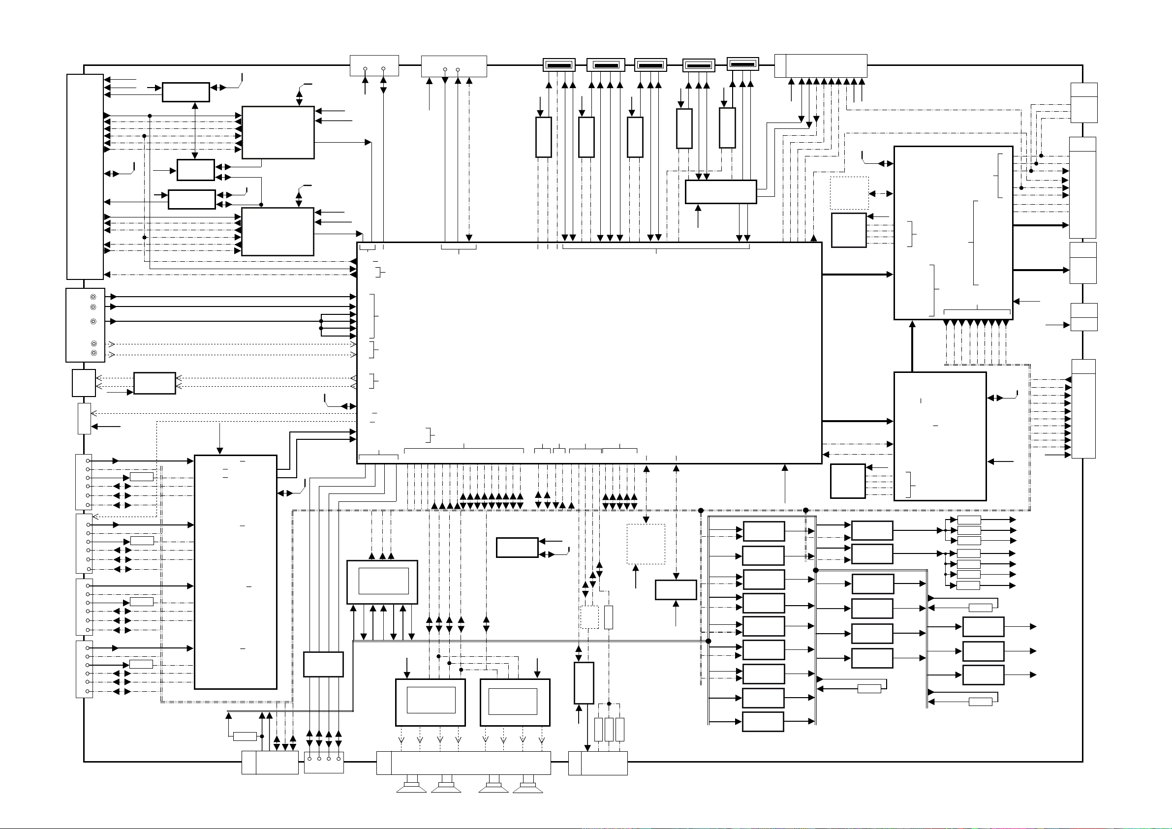
Block Diagram (1/3)
24
SUB3.3V
1,34
TU6708
JK3101
AUDIO
JK3104A
Digital
Audio Out
JK4704
JK4703
JK4701
JK4702
8,9
12
32
30,31
3,4
17,18
33
20,21
19
24
TUNER A/DVB-T/T2/C/S DUAL
27
22,23
Y/Vin,PB,PR
IN
HP-OUT
D3200
3_RX
3_HPD
5VDET3
DDCSDA3
HDMI1
DDCSCL3
CEC
2_RX
0_HPD
5VDET0
DDCSDA2
HDMI2
DDCSCL2
CEC
0_RX
2_HPD
5VDET2
DDCSDA0
HDMI3
DDCSCL0
CEC
1_RX
1_HPD
5VDET1
DDCSDA1
HDMI4
DDCSCL1
CEC
2
35
5
11
10
R
L
R
HP_L
HP_R
SUB3.3V
ASPDIFO0
SUB3.3V
EU_TU_1.8V
LNB_PWR1
IF2_P,N_T
IFAGC_T
T2_FEF0
FE_XRST_T
AGCBS2_T
BISQ-Q2,I2_T
IIC_2
LNB_PWR2
IF1_P,N_S
IFAGC1_S
T2_FEF1
EXT_AGCBS1_T
BISQ-Q1,I1_T
IFAGC2_T
COMP_D_PR
COMP_D_PB
LIN_Terminal
RIN_Terminal
COMP_D_Y
16V
9
IC3201
11
HP Amplifier
R4651
CEC
ASPDIFO1
R4515
CEC
R4545
CEC
R4521
SUB3.3V
CEC
12
IC6804
LNB
13
IC6806
8
DSQ_SW
16V
12
IC6805
LNB
13
13
15
3_RX
RX3P5VDET
DDCSDA3
DDCSCL3
2_RX
RX2P5VDET
DDCSDA2
DDCSCL2
0_RX
RX0P5VDET
DDCSDA0
DDCSCL0
1_RX
RX1P5VDET
DDCSDA1
DDCSCL1
IIC_2
6,7
3
IF2_P,N_T
IFAGC_T
T2_FEF0
DSQOUT_SW
1
7
6
6,7
3
IF1_P,N_S
IFAGC1_S
T2_FEF1
VDD3.3V
VDD1.1V
AVDD3.3V
AVDD3.3VRX
PVDD3.3V
AVDD1.1V
AVDD1.1VRX
42,43,45,46,48,49,51,52
TX0
22,24,25,27,28,30,31,33
TX1
70
8,10,11,13,14,16,17,19
74
75
55,56,58,59,61,62,64,65
71
76
77
93,94,96,97,99,100,102,103
IC4500
[MN864 778]
HDMI2.0 Rx
73
107
108
80,81,83,84,86,87,89,90
72
106
105
DCDCIN
38,37
48
47
29
26
31,32
DSQOUT_0
DSQOUT_1
IIC_2
DSQOUT_1
38,37
48
47
29
26
31,32
RX3
RX2
RX1
VJ2000
IC6800
[C1AB00004164]
DVB-T/T2/C/S/S2 DEM
23
23
IC6802
[C1AB00004164]
DVB-T/T2/C/S/S2 DEM
TX0
TX1
RX0
KEY1
STB5V
16V
9
3
10
1-5
A02
TO P2
IIC_2
SUB3.3V
20,21
45,46
TSCLK
20,21
20,21
46,47
IIC_1
3,4,5,8
45,46
3,4,5,8
IIC_2
T8600
9
DMD1.2/1.1V
Parallel TS
DEMOD_TSVAL
TSYNC
TSDATA0
SUB3.3V
DMD1.2/1.1V
Parallel TS
DEMOD_TSDATA1
TSDATA2
TSDATA3
TSDATA4
FE_XRST_T
IF2_P,N_T
IFAGC2_T
PR0P (R)
PB0P (G)
CVBS3P
AL0_ADAC
AR0_ADAC
IIC_0
IIC_1
IIC_2
11
14
RX-
TX-
RX+
POWER ON
TV_SUB_ON
7
11
12
6
JK8600
ETHERNET
SD SLOT
Demod
AT24
F37,F38
B14
J37
K36
Y0P (B)
L36
J38
SOY0
L37
COM0
K37
AIN_L0
D37
AIN_R0
B36
C35
D36
AB34
G27
RX1
B24,A24,B22,A22,D22,C22,D23,C23
RX0
B21,A21,B18,A18,B19,A19,B20,A20
Y38
RX-
1
16V
SUB9V
1 3 6 8
16
TX+
1 2 3
JK8650
3.3V
SDI0
LVDS/EPI/VB1
Audio Line in ADC
Audio DAC
Audio
Audio
ETHERNET
Y37
RX+
TV_SUB_ON
8
13
IC5000
[AN34043AAVF]
ANALOG ASIC
14
6 2
STB5V
DATA
Demod
Analog Video Input
W37 W38
TX-
DCDCEN
EASTERRST2
11
15
SUB5V
A12
JK6400A
CI SLOT
17,18
51,52
TS Paraller Input
GPI0, DEMOD
HDMI Receiver
E31
E34
F31
F34
F28
F30
TX+
3_HPD
2_HPD
1_HPD
0_HPD
3_PWR5V
2_PWR5V
MCLK
SDATA0
32
31
STB5V
SD3.3_1.8V
STB3.3V
16V
6
IC3800
[C1AB00003984]
AUDIO AMP
14,15
2 3
5
26,27
SP_L
9,16,25,32
10,11
R+ R- L- L+
1
A12
SP_R
CI DATA
TS Paraller Output
HDMI
G26
E30
D33
D34
1_PWR5V
0_PWR5V
3_DDCSCL
3_DDCSDA
2_DDCSDA
BCLK
LRCLK
8
7
30,31
WoR+
4
F33
G31
2_DDCSCL
SDATA1
6
10,11
5
Wo_R
G28
G30
1_DDCSCL
1_DDCSDA
0_DDCSDA
Temp.Sensor
7
8
IC38001
[C1AB00003984]
AUDIO AMP
14,15
WoR-
6
F27
F26
G24
CEC
0_DDCSCL
IC5911
5
9,16,25,32
26,27
WoL- WoL+
7
Wo_L
STB5V
1
3
PWM3
Other
P35
KEY1
16V
30,31
8
JK8705
WIFI
1
4
6
SW
IC8706
4
OPCTRL12
OPCTRL18
Power
Servo ADC inut
AB38
L35
POWER ON
TV_SUB_ON
SUB3.3V
IIC_1
2
3
USB_DP_P3(P)
USB_DM_P3(N)
Power
LVDS/EPI/VB1
Power
AD38
M34
BL_SOS
EASTERRST2
USB5V
1
4
OCP2
AT27
FAN_ON
Q5901
Q5902
Q5903
273
16V
A08
FAN_CTR1
JK8703
USB3
1
2,3 5,6
6
SW
IC8703
3
USB_DM(DP)_P2(P,N)
VBUS2
IC8000
[C1AB00004367]
AR27
AT28
AR28
FAN_SOS
FAN_CTR0
5
DC/DC
IC5901
D5905
FAN_VCC
1,4
15,18,
3,6,9,12
FAN
MTK
AP36
MCLK
FAN_SOS
8,9
SSUSB_RX(P,N)
AUDIO
AM31
BCLK
Q5904
D5906
7,10
1
USB5V
1
IC8701
3
SSUSB_TX(P,N)
VBUS0
AM30
AN31
AN30
LRCLK
SDATA0
SDATA1
DDR3 _ 5X4GB
SUB1.5V
D5904
13,16
JK8701
USB1
2
6
SW
4
USB_DM_P0(N)
OCP0
USB+GPI0
DDR I/F
IC8200
IC8201
IC8202
IC8203
IC8204
3
USB_DM_P0(P)
VBUS3
IC8920
eMMC 4GB
USB5V
1
3
VBUS1
eMMC
SUB3.3V
JK8702
USB2
1
2
6
SW
IC8702
4
USB0DN
HUB_OC1
25
3
SUB5V
3
USB0DP
4
IC8705
16V
16V
16V
DCDCIN
DCDCIN
DCDCIN
DCDCIN
DCDCIN
DCDCIN
USB HUB
DCDCEN
DCDCEN
DCDCEN
DCDCEN
DCDCEN
DCDCEN
DCDCEN
JK8706
4K-DEMO
(shop mode)
1
2
3
USB5V
1
6
SW
IC8707
4
3
VBUS3
HUB_OC2
USB1DN
USB1DP
7
6
24
15
16
1
2
USB_DP_P1(N)
USB_DM_P1(P)
2
3
4,5
8
1
12,23,26
5
14
4
5
5
4
4
8
5
4
1
5
5
4
4
5
2
4
5
2
4
BT_USB_DN
IC5220
DC/DC
IC5260
DC/DC
IC5200
DC/DC
IC8100
IC8100
DC/DC
DC/DC
IC8100
IC8101
DC/DC
DC/DC
IC8100
IC4450
DC/DC
DC/DC
IC8100
IC9150
DC/DC
DC/DC
IC8100
IC9160
DC/DC
DC/DC
IC8100
IC9170
DC/DC
DC/DC
A10
BT_USB_DP
Y35
LVDS,TCON,GPIO
STB3.3V
PHY3.3V
SUB1.0V
AVDD1.0V
STB_1.5V
SD3.3-1.8V
HDMI3.3V
USB5V
7,8
PNL12V
11
12
SUB3.3V
6
SUB1.0V
8
17
STB_1.5V
6
8
GE_1.1V
6
8
NT1.1V
8
8
NT1.5V
3
8
NT2.5V
3
8
TO K10/BT
3
4
2
12
REMOTE
BT_VBUS
U37
LVDS,GPIO
BT_USB_DP
BT_USB_DN
PANEL TEST_ON
AR25
AA33
AA34
AM22
AM35
AI_SENSOR
SUB5V
DCDCEN
SUB5V
DCDCEN
SUB5V
SUB5V
SUB5V
SUB3.3V
USB5V
SUB5V
G_LED_ON
7
1
8
6
STB3.3V
3D_LROUT
R_LED_ON
DDR3 _ 4X1GB
IC9200
IC9201
IC9202
IC9203
IC9600
SPI FLASH
V-By-One
V-By-One
GE_AMREADY
IC9900
SPI FLASH
V-By-One
2
5
4
7
8
5
4
5
3
1
5
2
4
3
10
SUB3.3V
IIC_0
SUB3.3V
8
SPI_CLK
6
5
2
1
GE_XRST
GE_3.3V
8
SPI_CLK
6
5
2
1
IC8100
IC4502
DC/DC
DC/DC
IC4506
Regulator
IC8631
Regulator
IC6405
Regulator
IC8100
IC5705
DC/DC
DC/DC
IC5704
Regulator
R5224
SPI_DO
SPI_DI
SPI_CS
SPI_DO
SPI_DI
SPI_CS
3
8
1
8
8
[C1AB00004293]
FRC DDR
AW29
AV29
AU29
AU28
AU6,AU5,AU4,AV4
AV5,AW5,AV6,AW6
AT7,AR7
AM7, AL7
AJ6,AK6,AL6,AL5
AL4,AM4,AM5,AM6
AN6,AP6,AP5,AP4
AR4,AR5,AR6,AT6
AF35,AE35
W37,W38,Y37,Y38
AA37,AA38,AB37,AB38
AC37,AC38,AD37,AD38
AE37,AE38,AF37,AF38
V-By-One TX
A6,A5
A15,B15,A14,B14
A13,B13,A12,B12
A11,B11,A10,B10
A9,B9,A8,B8
J38
R35
AP31
AP32
AR32
AP33
HDMI1.1V
HDMISW3.3V
3.3V
4
SUB_CI_5V
5
DMD1.2/1.1V
3
EU_TU_1.8V
4
IC9000
IC FRC (NTK)
FRC GPI0
V-By-One
SPI FLASH
SUB3.3V
STB5V
GE_3.3V
V-By-One TX
V-By-One RX
FRC GPI0
Y8V9T7
T9R9U7
FR_BL_SD0
FR_BL_VSYNC
FR_BL_SCK
FR_BL_HSYNC
V-By-One RX
IC4300
[C1AB00004358]
GCEX-2
IC IMAGE PROCESSOR
L4506
L4511
L4505
L4501
L4500
L4502
L4503
STB_1.5V
STB5V
8
4
8
SUB3.3V
GE_3.3V
G29
H29
K8,J8
K7,J7
C11,D11,E11,E10
E9,D9,C9,C8
D8,E8,E7,E6
D6,C6,D5,C5
D18,C18,C17,D17
E17,E16,E15,D15
C15,C14,D14,E14
E13,E12,D12,C12
U8
F27U9
FR_BL_SCS0
FR_BL_SCS1
FR_BL_SCS2
FR_BL_ON
GE_1.1V
GE_3.3V
GE_1.8V
VDD1.1V
AVDD1.1VRX
ADD1.1V
VDD3.3V
AVDD3.3V
ADD3.3VRX
PVD3.3V
F24
AF7
AG9
FR_BL_SCS3
IIC_0
FRC GPI0
D8106
1
3
1
AVDD1.0V
PHY3.3V
GE_1.8V
IC8102
Regulator
IC8601
Regulator
IC9901
Regulator
VJ9173
A-BOARD
[EXCHANGE UNIT]
PANEL TEST_ON
3D_LRID_OUT
V-By-One
V-By-One
NT1.1V
NT1.5V
NT2.5V
SUB3.3V
BL_SOS
FR_BL_HSYNC
FR_BL_VSYNC
FR_BL_SD0
FR_BL_SCK
FR_BL_SCS0
FR_BL_SCS1
FR_BL_SCS2
FR_BL_ON
FR_BL_SCS3
VCOM_WP
T_CON_SCL
T_CON_SDA
T_CON_SDA
T_CON_SCL
VCOM_WP
3D_ON
VTX_LOCK(0,1)
VTX_HTP(0,1)
PNL12V
SUB3.3V
A18
1
4
3
A16
34
33
32
29
36
35
26
27
2,3,5,6
8,9,11,12
14,15,17,18
20,21,23,24
A15
18,19,21,22
24,25,27,28
30,31,33,34
36,37,39,40
A17
3-5
A03
1
2
4
6
8
10
12
14
15
16
11,13
SERVICE
TO PANEL
(CNV1)
TO PANEL
(CNV2)
TO PANEL
(TCON)
TO PANEL
(LD)
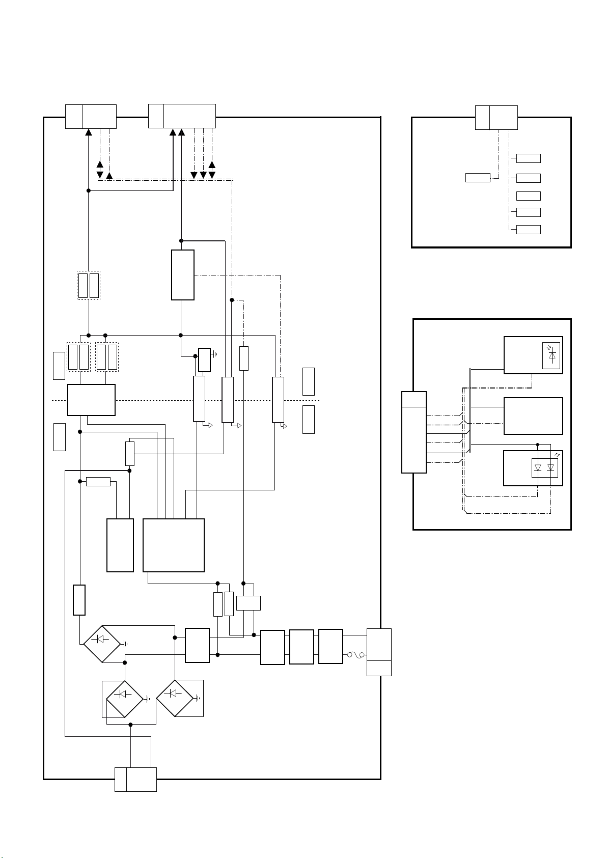
Block Diagram (2/3)
~
~
+
-
Line
~
~
+
-
~
~
+
-
25
COLD
T7301
HOT
P3
D7419
9
4
TO PB3
1
16V
POWER_ON
Q7405
Q7403
D7418
6
Q7203
4
KEY
D7417
14
5
D7416
OUT
7
IC7201
Power
Controller
Q7202
8 VCC
14 VS
IC7301
1VH
P2
Current
Resonant
TO A02
1- 5
16V
8 VW
10 VCC
Controller
9
11
SUB_ON
5VS
8
3
DC/DC
IC7405
2
PC7301
9 PGS
12
10
KEY
POWER_ON
IC7401
Photo coupler
PC7302
FB
4
SUB_ON
Q7412
Photo coupler
Photo coupler
PC7303
P-BOARD
HOT COLD
GK-BOARD
K-BOARD
K10
1
2
3
4
TO A10
5
7
R LED
G LED
STBY 3.3V
AI
SUB3.3V
REMOTE
SW2857
STBY 3.3V
SUB3.3V
AI
STBY 3.3V
R LED
G LED
TO PB5
GK4
POWER_ON
3
KEY
VCC
REMOTE
2
4
D2802
2
SW2851
SW2852
SW2853
SW2854
SW2855
RM2800
OUT
VCC
SN2800
OUT
AI
G
R
3
T7201
1
1
D7112
D7114
SRV-AC
SRV-VCC
4
1
P6
TO PB6
D7116
LF7108
Line
Filter
D7104
RL7106
D7105
LF7107
Line
Filter
LF7106
Filter
LF7105
Line
Filter
F7101
2
1
P1
MAIN INPUT
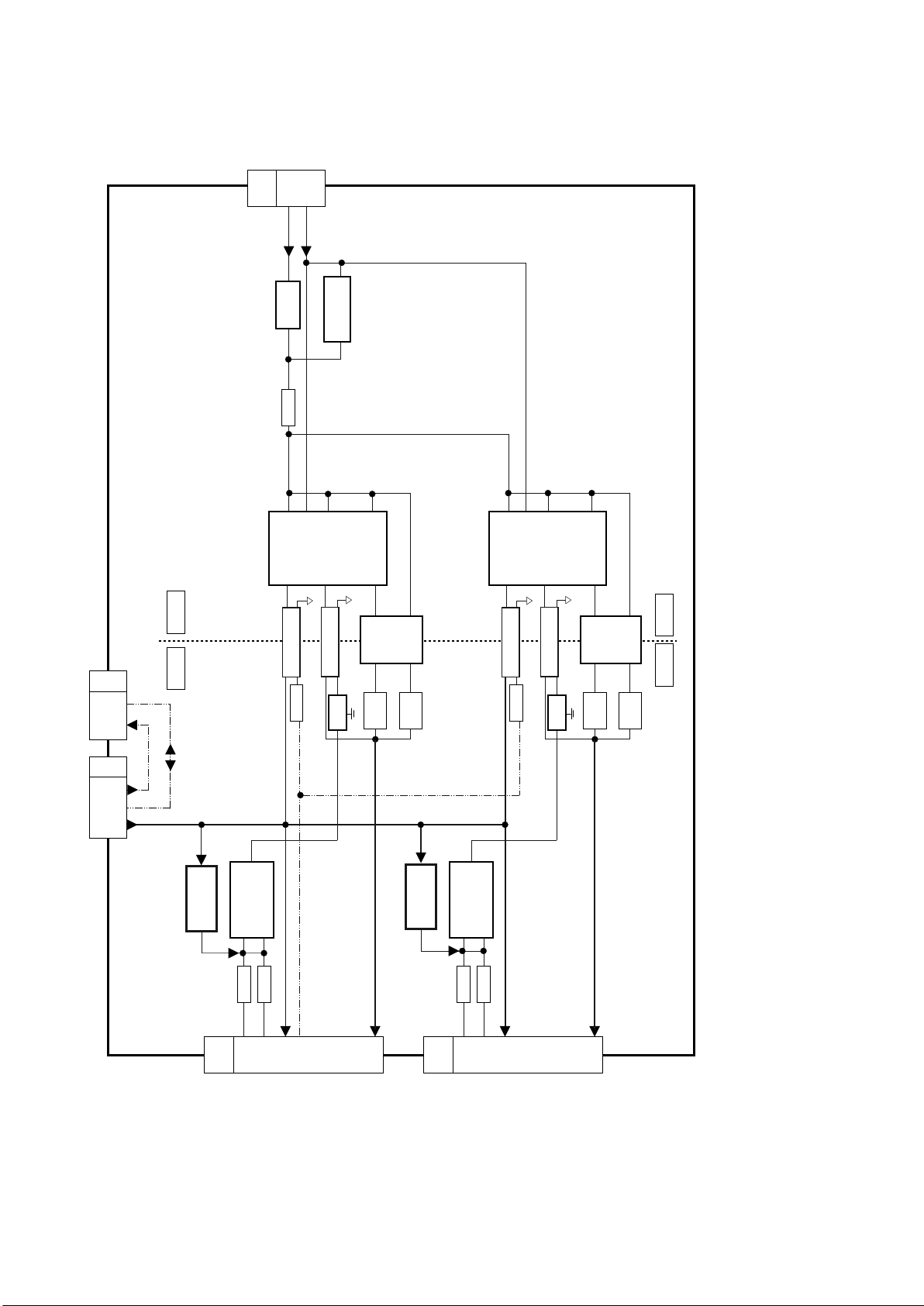
Block Diagram (3/3)
26
TO P6
1
PB6
SRV-AC
4
PB-BOARD
SRV-VCC
TO GK4
PB5
3
2
HOT
COLD
2 1
T7650
D7656
14VS
STB
6
Photo coupler
PC7501
Q7550
10VCC
PC7500
8
IC PFC
IC7650
7
15H0
IC7500
Resonant
Controller
4FB
T7500
Photo coupler
IC7550
11L0
VW
9
10,12 4
D7550
D7552
3
5,7
D7551
D7553
14VS
STB
6
Photo coupler
PC7526
Q7576
10VCC
PC7525
15H0
IC7525
Resonant
Controller
4FB
T7525
Photo coupler
IC7575
11L0
9VW
10,12 1
D7575
D7577
2
5,7
D7576
D7578
HOT
COLD
TO P3
PB3
5
4
1
KEY
16V
POWER_ON
16V
5
IC7900
1
Regulator
PB1
IC7901
5
Q7900
PWM
1,2
3,4
Amplifier
IC Operational
1
Q7902
FB
3,4
TO PANEL
LDA/LDB
16V
BL_ON
9,10
16V
5
IC7925
1
VLED
5
17-28
Regulator
PB2
IC7926
5
Q7925
PWM
1,2
3,4
Amplifier
IC Operational
1
Q7927
FB
3,4
TO PANEL
LDC/LDD
16V
9,10
VLED
17-28
Parts Location
27
7
1
8
36
22
3
30
31
32

Parts Location
28
18
12
17
16
13
Bottom View:
Front View:
Uppert View:
SCREWS
THTD030J /4pcs/
18
19
12
SCREWS
XYN4+F15FJK /4pcs/
XYN4+F25FJK /2pcs/
15
Bottom View:
Bottom View:
14

Parts Location
29
56*
44
6
42
44
6
42
9
44
SCREWS
THEJ036J /7pcs/
Rear Side View
6
41
38
28
20
5
10
26
43
BOTTOM BACK COVER
FK201 FK202
FK203 FK204
56* - when replacing the LCD panel order also the WIFI Bracket (26) and the BT Bracket (27)
45
2523
4
K PCB
23
43
21
24
40
39
37
29
11
27
Location of Lead Wiring
A
A
A
A
A
A
A
A
30
53
47 35
52
33
34
48
49
LD
LDA
FAN1 FAN2
55
LDB
GK4
PB1
PB5
PB6
LDC
PB2
PB3
FAN3 FAN4
P6
P3
FAN6
FAN5
08
03
02
15
P2
P1
16
17
12
JK8705
10
WIFI
LDD
54
SP_R
2
CNV2
46
CNV1
TCON
51
50
K10
SP_L
BT
 Loading...