

Panasonic TH-42PH10BK, TH-42PH10BS, TH-42PH10EK, TH-42PH10ES Service manual
y
A
A
Y
Y
OR D ER NO . PC Z07 05048CE
High Definition Plasma Display
TH-42PH10BK
TH-42PH10BS
TH-42PH10EK
TH-42PH10ES
GPH10D Chassis
Specifications
Power Source 220-240 VAC, 50/60Hz
Power Consumption
Power on 365 W
Stand-bycondition Save OFF 1.0 W, Save ON 0.8 W
Power off condition 0.5 W
Plasma Displaypanel Drive method:AC type 42-inch,
16:9 aspect ratio
Contrast Ratio Max10000:1
Screen size 36.2” (922 mm) (W) × 20.4” (518 mm) (H) × 42” (1,057 mm) (diagonal)
(No. of pixels) 786,432 (1,024 (W) × 768 (H))
[3,072 × 768 dots]
Operating condition
Temperature 0 °C - 40 °C
Humidit
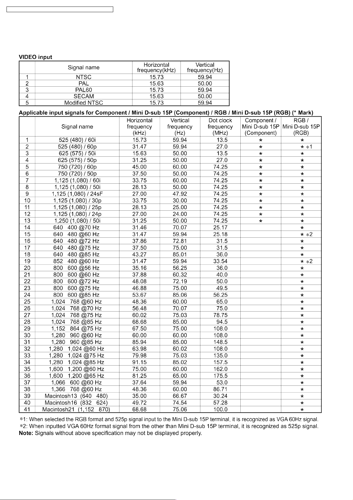
Applicablesignals
Color System NTSC, PAL, PAL60, SECAM, Modified NTSC
Scanning format 525 (480) / 60i 60p, 625 (575)/50i 50p, 750 (720)/60p 50p, 1125 (1080) / 60i 50i 24p 25p
PC signals VGA, SVGA, XGA,
20 % - 80 %
30p 24sF .... SMPTE274M, 1250 (1080) / 50i
SXGA, UXGA..... (compressed)
Horizontal scanning frequency 15 - 110 kHz
Vertical scanning frequency 48 - 120 Hz
Connection terminals
VIN VIDEO IN (BNC) 1.0 Vp-p (75-ohm)
S VIDEO IN (MINI DIN 4PIN) Y: 1 Vp-p (75-ohm), C: 0.286 Vp-p (75-ohm)
UDIO IN (RCA PIN JACK × 4) 0.5 Vrms (high impedance)
PC IN (HIGH-DENSITYMini-D-SUB 15PIN)
or G with/sync1.0 Vp-p (75-ohm)
or G without / sync0.7 Vp-p (75-ohm)
© 2007 Matsushita Electric Industrial Co., Ltd. All
rights reserved. Unauthorized copying and
distribution is a violation of law.
/
/
A
y
TH-42PH10BK / TH-42PH10BS / TH-42PH10EK / TH-42PH10ES
B/P
CB:0.7 Vp-p (75-ohm)
B
R/P
VBS (use HD port) with/picture 1.0 Vp-p (high impedance)
UDIO IN (M3 JACK) 0.5 Vrms (high impedance)
SERIAL EXTERNAL CONTROL TERMINAL (D-SUB 9PIN) RS-232C COMPATIBLE
SPEAKERS (6-ohm) 16 W [8 W + 8 W] (10 % THD)
Accessories Supplied
Remote Control Transmitter EUR7636090R
Batteries 2 × R6 Size
Fixing bands TMME203 × 2
Dimensions (W×H×D) 40.2” (1,020 mm) × 24” (610 mm) × 3.5” (89 mm)
Mass (weight)
main unit onl
with speakers approx. 30.0 kg
approx. 26.0 kg net
CR:0.7 Vp-p (75-ohm)
R
HD/VD:1.0 - 5.0 Vp-p (high impedance)
without/picture 0.3 Vp-p (high impedance)
Notes:
· Design and specifications are subject to change without notice. Mass and dimensions shown are approximate.
· This equipment complies with the EMC standards listed below.EN55022, EN55024, EN61000-3-2, EN61000-3-3.
CONTENTS
Page Page
1 Applicable signals 4
2 Safety Precautions
2.1. General Guidelines
2.2. Touch-Current Check
3 Prevention of Electrostatic Discharge (ESD) to
Electrostatically Sensitive (ES) Devices
4 About lead free solder (PbF)
5 Service Hint
6 Disassembly
6.1. Removal of Rear Cover
6.2. Removal of HU-Board
6.3. Removal of Slot Block
6.4. Removal of DS-Board
6.5. Removal of HX-Board
6.6. Removal of DN-Board
6.7. Removal of P-Board
6.8. Removal of D-Board
6.9. Removal of H3-Board (L, R)
6.10. Removal of SU-Board and SD-Board
6.11. Removal of SC-Board
6.12. Removal of SS-Board
6.13. Removal of C1, C2-Board
6.14. Removal of S1-Board
6.15. Removal of Fan
6.16. Removal of Escutcheon
10
10
10
11
11
11
11
12
12
12
13
13
14
6.17. Removal of V1-Board and V2-Board
5
5
5
6
7
8
9
9
9
9
6.18. Removal of Plasma Panel
7 Location Lead Wiring
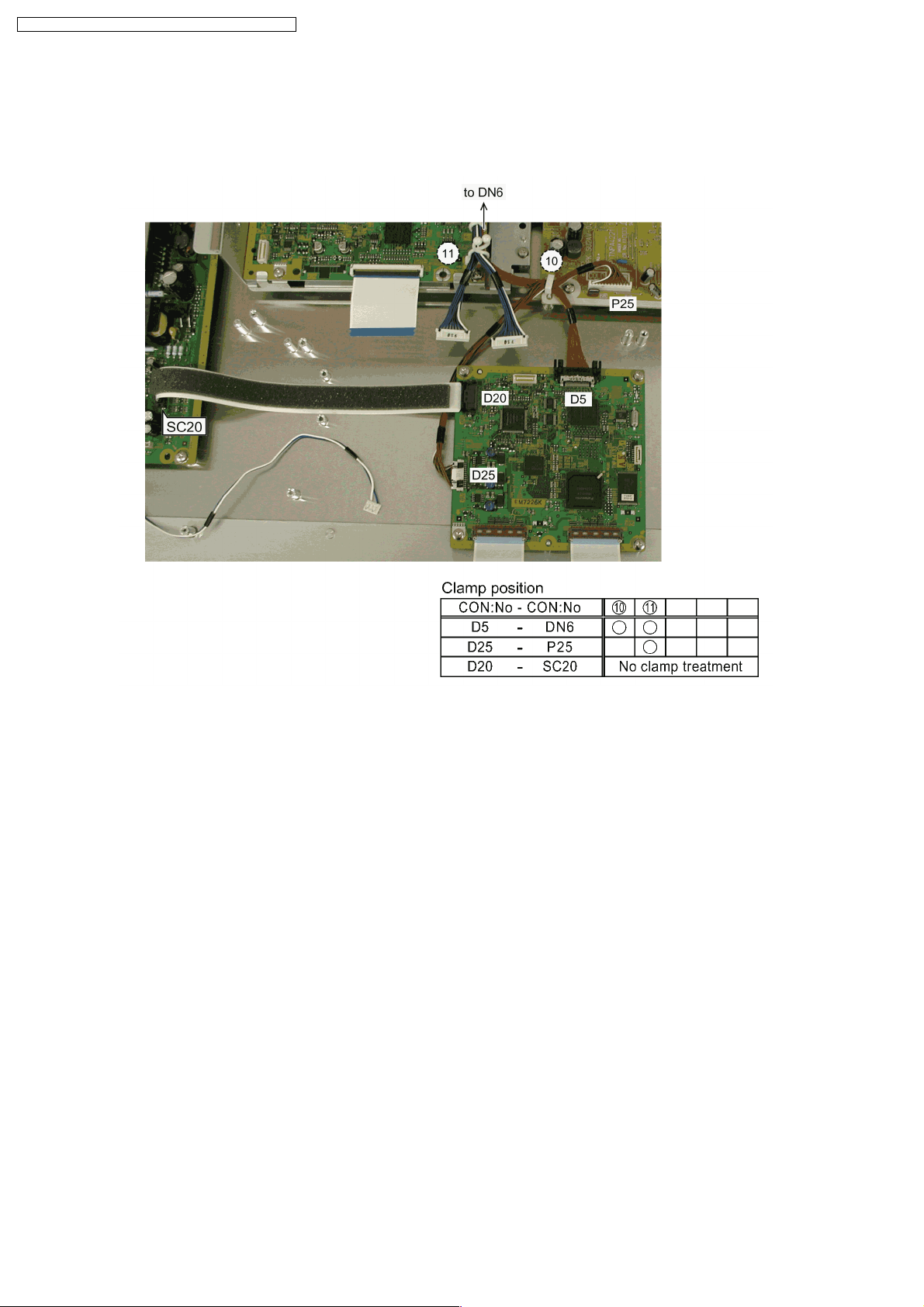
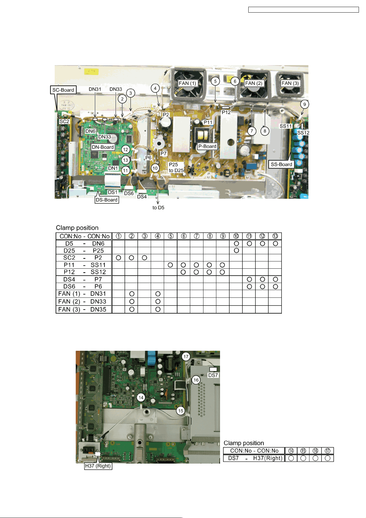
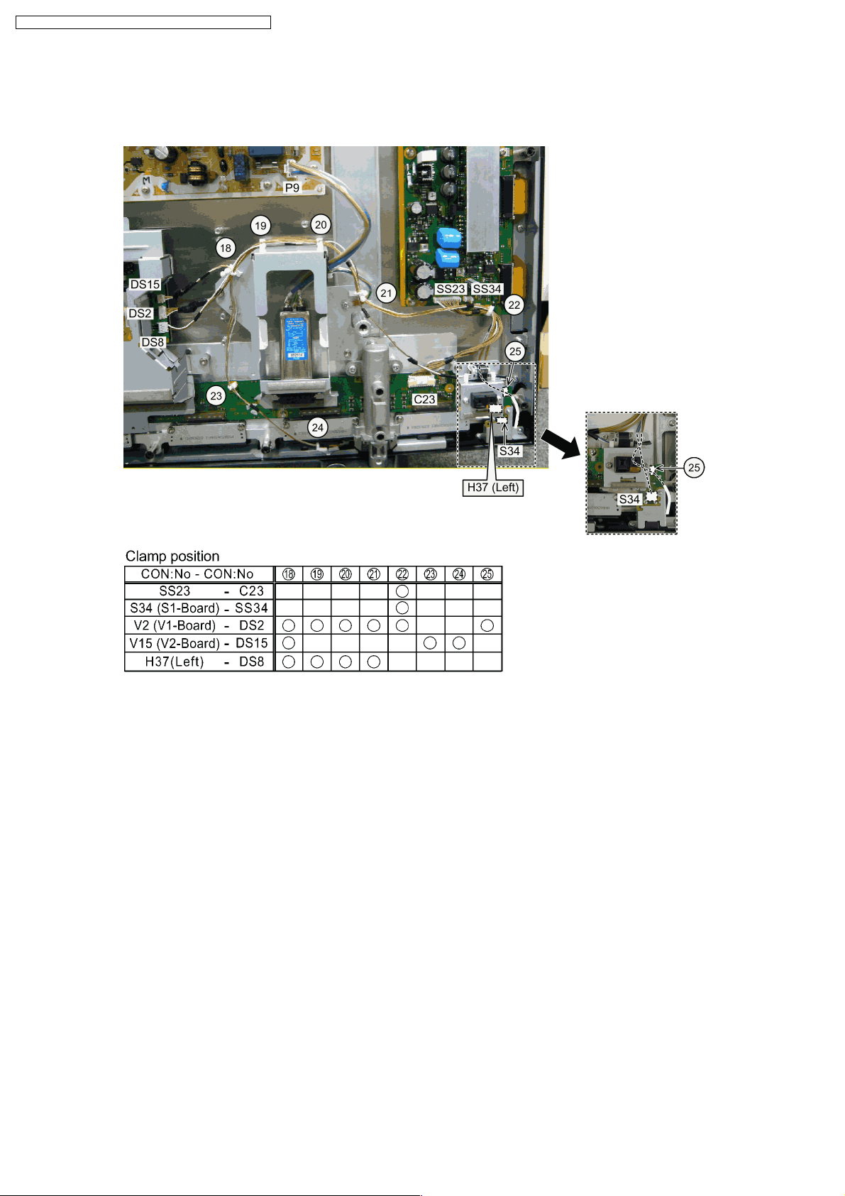
7.1. Lead Wiring (1)
7.2. Lead wiring (2)
7.3. Lead wiring (3)
7.4. Lead Wiring (4)
8 Adjustment Procedure
8.1. Driver Set-up
8.2. Initialization Pulse Adjust
8.3. P.C.B. (Printed Circuit Board) exchange
8.4. Adjustment Volume Location
8.5. Test Point Location
9 Service mode
9.1. CAT (computer Aided Test) mode
9.2. IIC mode structure (following items value is sample data.)
10 Adjustment
10.1. RGB white balance adjustment
10.2. HD white balance adjustment
10.3. Power control adjustment
11 Trouble shooting guide
11.1. Self Check
11.2. No Power
11.3. No Picture
14
15
18
18
19
19
20
21
21
22
22
23
23
24
24
28
29
29
31
33
34
34
36
36
2

TH-42PH10BK / TH-42PH10BS / TH-42PH10EK / TH-42PH10ES
11.4. Local screen failure 37
12 Option Setting
13 Conductor Views
13.1. P-Board
13.2. HU-Board
13.3. HX-Board
13.4. H3, S1, V1 and V2-Board
13.5. DS-Board
13.6. DN-Board
13.7. D-Board
13.8. C1-Board
13.9. C2-Board
13.10. SC-Board
13.11. SU-Board
13.12. SD-Board
13.13. SS-Board
14 Block and Schematic Diagram
14.1. Schematic Diagram Notes
14.2. Main Block Diagram
14.3. P-Board Block Diagram
14.4. P-Board (1 of 6) Schematic Diagram
14.5. P-Board (2 of 6) Schematic Diagram
14.6. P-Board (3 of 6) Schematic Diagram
14.7. P-Board (4 of 6) Schematic Diagram
14.8. P-Board (5 of 6) Schematic Diagram
14.9. P-Board (6 of 6) Schematic Diagram
14.10. HU-Board Block Diagram
14.11. HU-Board (1 of 2) Schematic Diagram
14.12. HU-Board (2 of 2) Schematic Diagram
14.13. HX-Board Block and Schematic Diagram
14.14. V1 and V2-Board Block and Schematic Diagram
14.15. DS-Board (1 of 2) and H3-Board Block Diagram
14.16. DS-Board (2 of 2) Block Diagram
14.17. DS-Board (1 of 5)Schematic Diagram
14.18. DS-Board (2 of 5) and H3-Board Schematic Diagram
14.19. DS-Board (3 of 5) Schematic Diagram
14.20. DS-Board (4 of 5) Schematic Diagram
14.21. DS-Board (5 of 5) Schematic Diagram
14.22. DN-Board (1 of 2) Block Diagram
14.23. DN-Board (2 of 2) Block Diagram
14.24. DN-Board (1 of 6) Schematic Diagram
38
41
41
44
45
46
47
49
51
53
54
55
58
59
60
63
63
64
65
66
67
68
69
70
71
72
73
74
75
76
77
78
79
80
81
82
83
84
14.25. DN-Board (2 of 6) Schematic Diagram
14.26. DN-Board (3 of 6) Schematic Diagram
14.27. DN-Board (4 of 6) Schematic Diagram
14.28. DN-Board (5 of 6) Schematic Diagram
14.29. DN-Board (6 of 6) Schematic Diagram
14.30. D-Board Block Diagram
14.31. D-Board (1 of 6) Schematic Diagram
14.32. D-Board (2 of 6) Schematic Diagram
14.33. D-Board (3 of 6) Schematic Diagram
14.34. D-Board (4 of 6) Schematic Diagram
14.35. D-Board (5 of 6) Schematic Diagram
14.36. D-Board (6 of 6) Schematic Diagram
14.37. C1 and C2-Board Block Diagram
14.38. C1-Board (1 of 2) Schematic Diagram
14.39. C1-Board (2 of 2) Schematic Diagram
14.40. C2-Board (1 of 2) Schematic Diagram
14.41. C2-Board (2 of 2) Schematic Diagram
14.42. SC-Board Block Diagram
14.43. SC-Board (1 of 2) Schematic Diagram
14.44. SC-Board (2 of 2) Schematic Diagram
14.45. SU and SD-Board (1 of 2) Block Diagram
14.46. SU-Board (1 of 2) Schematic Diagram
14.47. SU-Board (2 of 2) Schematic Diagram
14.48. SD-Board (1 of 2) Schematic Diagram
14.49. SD-Board (2 of 2) Schematic Diagram
14.50. SS and S1-Board Block Diagram
14.51. SS-Board (1 of 2) and S1-Borad Schematic Diagram
14.52. SS-Board (2 of 2) Schematic Diagram
15 Parts Location
15.1. Exploded View
15.2. Escutcheon part location enlarged view
15.3. Fan part location enlarged view
15.4. Cable relation
15.5. Packing summary
16 Mechanical Replacement Parts List
17 Replacement Parts List
17.1. Replacement Parts List Notes
17.2. Electrical Replacement Parts List
85
86
87
88
89
90
91
92
93
94
95
96
97
98
99
100
101
102
103
104
105
106
107
108
109
110
111
112
113
114
115
115
116
116
117
118
120
121
121
122
3
TH-42PH10BK / TH-42PH10BS / TH-42PH10EK / TH-42PH10ES
1 Applicable signals
4
TH-42PH10BK / TH-42PH10BS / TH-42PH10EK / TH-42PH10ES
2 Safety Precautions
2.1. General Guidelines
1. When conducting repairs and servicing, do not attempt to modify the equipment, its parts or its materials.
2. When wiring units (with cables, flexible cables orlead wires) are supplied as repair parts and only one wireor some of the wires
have been broken or disconnected, do not attempt to repair or re-wire the units. Replace the entire wiring unit instead.
3. When conducting repairs and servicing, do nottwist the Faston connectors but plug them straight in or unplug them straight out.
4. When servicing, observe the original lead dress.If a short circuit is found, replace all parts which have been overheated or
damaged by the short circuit.
5. After servicing, see to it that all the protective devices such as insulation barriers, insulation papers shields are properly
installed.
6. After servicing, make the following leakage current checks to prevent the customer from being exposed to shock hazards.
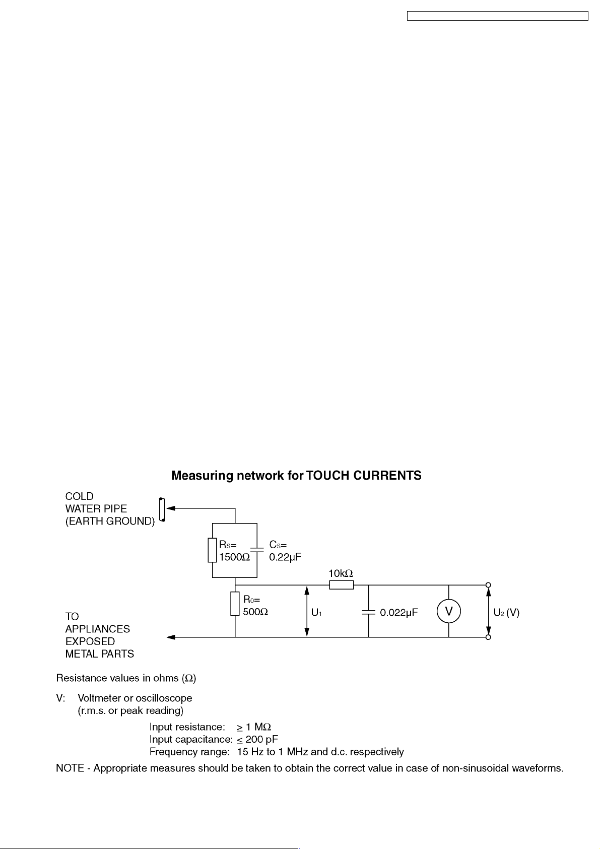
2.2. Touch-Current Check
1. Plug the AC cord directly into the AC outlet. Do not use an isolation transformer for this check.
2. Connect a measuring network for touch currents between each exposed metallic part on the set and a good earth ground such
as a water pipe, as shown in Figure 1.
3. Use Leakage Current Tester (Simpson 228 or equivalent) to measure the potential across the measuring network.
4. Check each exposed metallic part, and measure the voltage at each point.
5. Reserve the AC plug in the AC outlet and repeat each of the above measure.
6. The potential at any point (TOUGH CURRENT) expressed as voltage U
For a. c.: U
For d. c.: U
Note:
The limit value of U
mA d. c.
The limit value U
7. In case a measurement is out of the limits specified, there is a possibility of a shock hazard, and the equipment should be
repaired and rechecked before it is returned to the customer.
= 35 V (peak) and U2= 0.35 V (peak);
1
= 1.0 V,
1
= 0.35 V (peak) for a. c. and U1= 1.0 V for d. c. correspond to the values 0.7 mA (peak) a. c. and 2.0
2
= 35 V (peak) for a. c. correspond to the value 70 mA (peak) a. c. for frequencies greater than 100 kHz.
1
and U2, does not exceed the following values:
1
Figure 1
5
TH-42PH10BK / TH-42PH10BS / TH-42PH10EK / TH-42PH10ES
3 Prevention of Electrostatic Discharge (ESD) to
Electrostatically Sensitive (ES) Devices
Some semiconductor (solid state) devices can be damaged easily by static electricity. Such components commonly are called
Electrostatically Sensitive (ES) Devices. Examples of typical ES devices are integrated circuits and some field-effect transistors and
semiconductor "chip" components. The following techniques should be used to help reduce the incidence of component damage
caused by electrostatic discharge (ESD).
1. Immediately before handling any semiconductor component or semiconductor-equipped assembly, drain off any ESD on your
body by touching a known earth ground. Alternatively, obtain and wear a commercially available discharging ESD wrist strap,
which should be removed for potential shock reasons prior to applying power to the unit under test.
2. After removing an electrical assembly equipped with ES devices, place the assembly on a conductive surface such as
aluminum foil, to prevent electrostatic charge buildup or exposure of the assembly.
3. Use only a grounded-tip soldering iron to solder or unsolder ES devices.
4. Use only an anti-static solder removal device. Some solder removal devices not classified as "anti-static (ESD protected)" can
generate electrical charge sufficient to damage ES devices.
5. Do not use freon-propelled chemicals. These can generate electrical charges sufficient to damage ES devices.
6. Do not remove a replacement ES device from its protective package until immediately before you are ready to install it. (Most
replacement ES devices are packaged with leads electrically shorted together by conductive foam, aluminum foil or comparable
conductive material).
7. Immediately before removing the protective material from the leads of a replacement ES device, touch the protective material
to the chassis or circuit assembly into which the device will be installed.
Caution
Be sure no power is applied to the chassis or circuit, and observe all other safety precautions.
8. Minimize bodily motions when handling unpackaged replacement ES devices. (Otherwise ham lessmotion such as the brushing
together of your clothes fabric or the lifting of your foot from a carpeted floor can generate static electricity (ESD) sufficient to
damage an ES device).
6
TH-42PH10BK / TH-42PH10BS / TH-42PH10EK / TH-42PH10ES
4 About lead free solder (PbF)
Note: Lead is listed as (Pb) in the periodic table of elements.
In the information below, Pb will refer to Lead solder, and PbF will refer to Lead Free Solder.
The Lead Free Solder used in our manufacturing process and discussed below is (Sn+Ag+Cu).
That is Tin (Sn), Silver (Ag) and Copper (Cu) although other types are available.
This model uses Pb Free solder in it’s manufacture due to environmental conservation issues. For service and repair work, we’d
suggest the use of Pb free solder as well, although Pb solder may be used.
PCBs manufactured using lead free solder will have the PbF within a leaf Symbol PbF stamped on the back of PCB.
Caution
·Pb free solder has a higher melting point than standard solder. Typically the melting point is 50 ~ 70 °F (30~40 °C) higher.
Please use a high temperature soldering iron and set it to 700 ± 20 °F (370 ± 10 °C).
·Pb free solder will tend to splash when heated too high (about 1100 °F or 600 °C).
If you must use Pb solder, please completely remove all of the Pb free solder on the pins or solder area before applying Pb
solder. If this is not practical, be sure to heat the Pb free solder until it melts, before applying Pb solder.
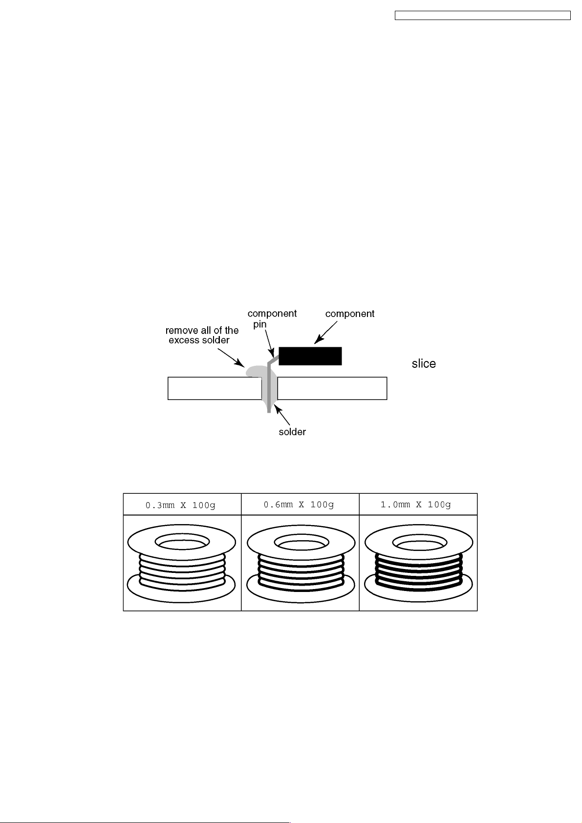
·After applying PbF solder to double layered boards, please check the component side for excess solder which may flow onto
the opposite side. (see figure below)
Suggested Pb free solder
There are several kinds of Pb free solder available for purchase. This product uses Sn+Ag+Cu (tin, silver, copper) solder.
However, Sn+Cu (tin, copper), Sn+Zn+Bi (tin, zinc, bismuth) solder can also be used.
7
TH-42PH10BK / TH-42PH10BS / TH-42PH10EK / TH-42PH10ES
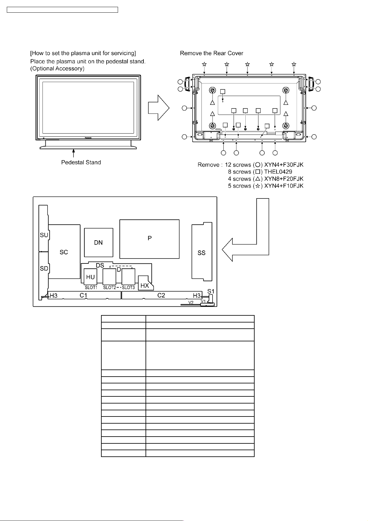
5 Service Hint
Board Name Function
DN Digital Signal Processor, Microcomputer
D Format Converter, Plasma AI Processor
DS Slot Interface (Audio / Video / Sync Input
SS Sustain drive
SC Scan drive
SU Scan out (Upper)
SD Scan out (Lower)
C1 Data Drive (Right)
C2 Data Drive (Left)
H3 Speaker terminal
S1 Power switch
V1 Remote receiver, LED-G, R
V2 Key switch
P Power supply
HX PC / RS-232C_Input terminal
HU Dual Video terminal (BNC / S)
Sub-Field Processor
Switch),
SYNC Processor, Audio Processor,
Speaker Out Amplifier,
DC-DC Converter
Note:
·Extension cable kit Slot Board is supplied as service fixtures and tools.
(Parts No. TZSC0704)
8
TH-42PH10BK / TH-42PH10BS / TH-42PH10EK / TH-42PH10ES
6 Disassembly
·To disassemble P.C.B., wait for 1 minute after power was
off for discharge from electrolysis capacitors.
and marks indicate screw positions.
·
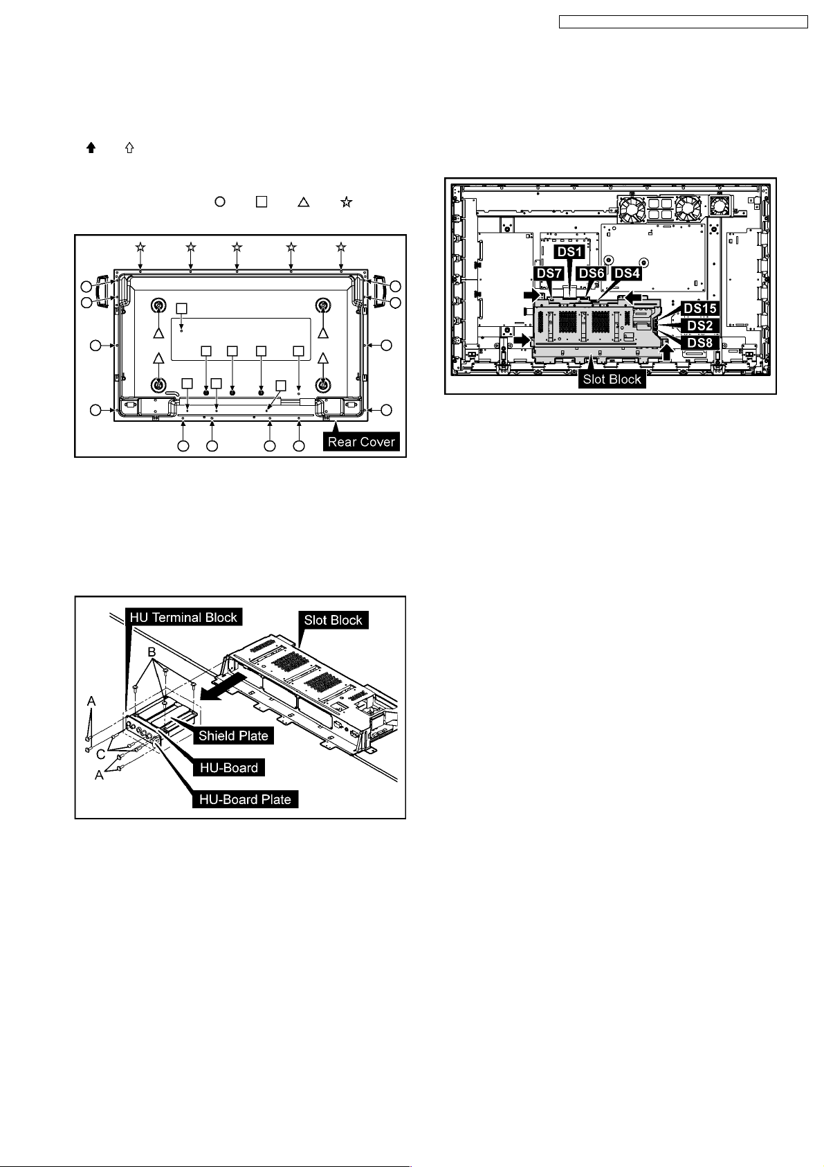
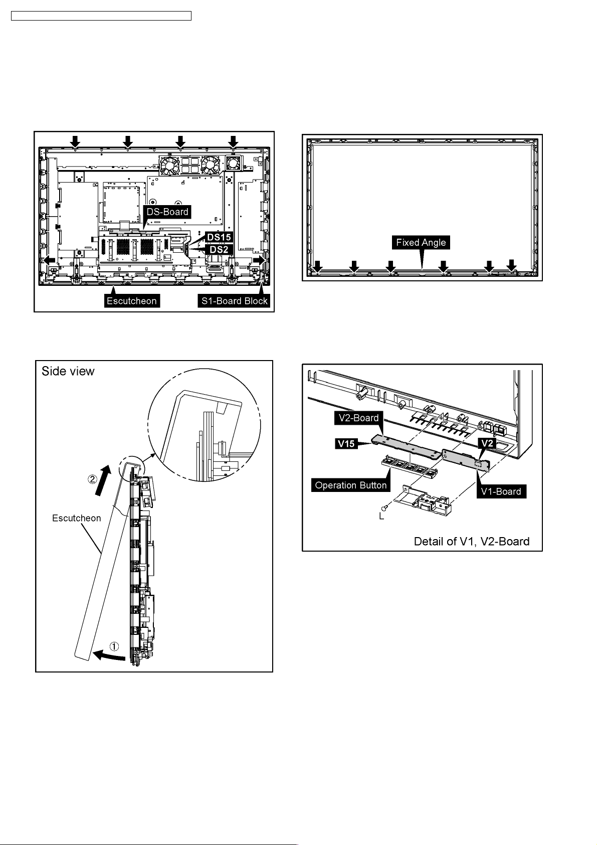
6.1. Removal of Rear Cover
1. Remove screws (×12 ,×8 ,×4 ,×5 ) and then
remove the Rear Cover.
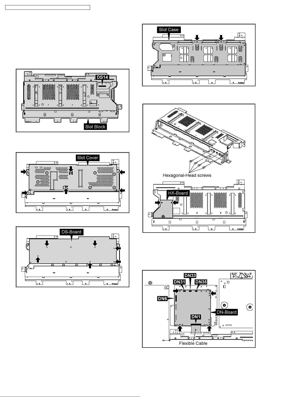
6.3. Removal of Slot Block
1. Disconnect the connectors (DS2, DS4, DS6, DS7, DS8,
DS15).
2. Remove the Flexible Cable from the connector (DS1).
3. Remove 4 screws and then remove the Slot Block.
6.2. Removal of HU-Board
1. Remove 4 screws (A) and then remove the HU Terminal
Block.
2. Remove 4 screws (B).
3. Remove 3 screws (C) and then remove HU-Board.
9
TH-42PH10BK / TH-42PH10BS / TH-42PH10EK / TH-42PH10ES
6.4. Removal of DS-Board
1. Remove the HU Terminal Block.
(Refer to Removal of HU-Board)
2. Remove the Slot Block.
(Refer to Removal of Slot Block)
3. Disconnect the connector (DS14).
4. The Slot Block is turned inside out.
5. Remove 6 screws and then remove the Slot Cover.
5. Remove 4 Hexagonal-Head screws and 2 screws and then
remove HX-Board.
6. Remove 6 screws and then remove DS-Board.
6.5. Removal of HX-Board
1. Remove the HU Terminal Block.
(Refer to Removal of HU-Board)
2. Remove the Slot Block.
(Refer to Removal of Slot Block)
3. Remove the DS-Board.
(Refer to Removal of DS-Board)
4. Remove 2 screws and then remove the Slot Case.
6.6. Removal of DN-Board
1. Disconnect the connectors (DN6, DN31, DN33, DN35).
2. Remove the Flexible Cable from the connector (DN1).
3. Remove 4 screws and then remove DN-Board.
Note:
A re-setup of the destination is performed by MS mode
after DN-Board exchange.
10
6.7. Removal of P-Board
1. Disconnect the connectors (P2, P6, P7, P9, P11, P12, P25)
2. Remove 10 screws and then remove P-Board.
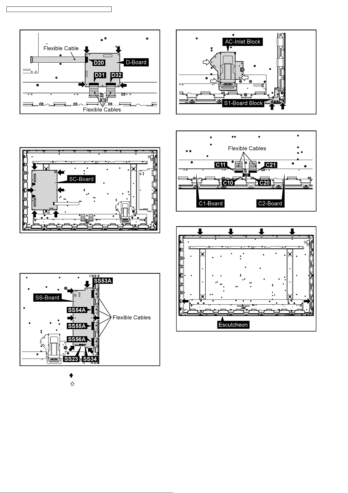
6.8. Removal of D-Board
TH-42PH10BK / TH-42PH10BS / TH-42PH10EK / TH-42PH10ES
6.10. Removal of SU-Board and SDBoard
1. Remove the Flexible Cables from the connectors (SU1,
SU2, SU3, SU4, SD1, SD2, SD3, SD4).
2. Remove 3 screws.
1. Remove the Slot Block.
(Refer to Removal of Slot Block)
2. Disconnect the connectors (D5, D20, D25)
3. Remove the Flexible Cables from the connectors (D31,
D32).
4. Remove 4 screws and then remove D-Board.
6.9. Removal of H3-Board (L, R)
1. Remove 2 screws and then remove the Speaker Terminal
Block (L, R).
3. Disconnect the connectors (SU45, SD46).
4. Slide SU-Board and SD-Board to the left to remove SUBoard and SD-Board from the connectors (SC41, SC42).
2. Disconnect the connector (H37).
3. Remove 3 screws (G) and then remove H3-Board.
11
TH-42PH10BK / TH-42PH10BS / TH-42PH10EK / TH-42PH10ES
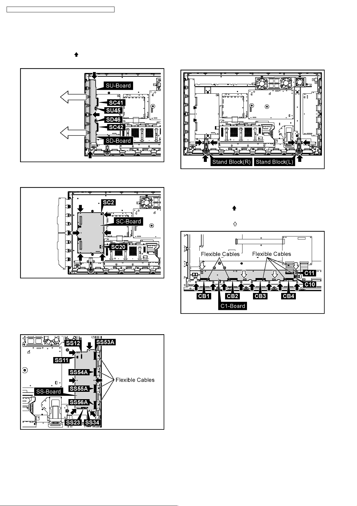
6.11. Removal of SC-Board
1. Disconnect the connectors (SU45, SD46).
2. Remove 3 screws (
Board to the left.
3. Disconnect the connectors (SC2, SC20).
4. Remove 6 screws and then remove SC-Board.
) and then slide SU-Board and SD-
6.13. Removal of C1, C2-Board
1. Remove the Slot Block.
(Refer to Removal of Slot Block)
2. Remove 6 screws and then remove the Stand Block (L, R).
6.13.1. Removal of C1-Board
1. Remove the Flexible Cables from the connectors (C10,
C11).
2. Remove 8 screws (
from the connectors (CB1, CB2, CB3, CB4).
3. Remove 4 screws (
) and then remove the Flexible Cables
) and then remove C1-Board.
6.12. Removal of SS-Board
1. Disconnect the connectors (SS11, SS12, SS23, SS34).
2. Remove the Flexible Cables from the connectors (SS53A,
SS54A, SS55A, SS56A).
3. Remove 6 screws and then remove SS-Board.
12
TH-42PH10BK / TH-42PH10BS / TH-42PH10EK / TH-42PH10ES
6.13.2. Removal of C2-Board
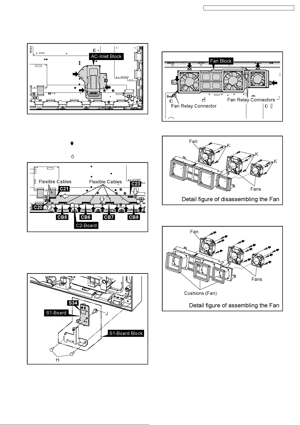
1. Remove 3 screws and then remove the AC-Inlet Block.
2. Remove the Flexible Cables from the connectors (C20,
C21).
3. Disconnect the connector (C23).
4. Remove 8 screws (
from the connectors (CB5, CB6, CB7, CB8).
5. Remove 4 screws (
) and then remove the Flexible Cables
) and then remove C2-Board.
6.15. Removal of Fan
1. Remove 4 screws and then remove the Fan Block.
2. Disconnect the Fan Relay Connectors.
3. Remove 12 screws (K) and then remove the Fans.
6.14. Removal of S1-Board
1. Remove 2 screws (H) and then remove the S1-Board Block.
2. Disconnect the connector (S34).
3. Remove 1 screw (J) and then remove S1-Board.
4. Reassemble the Fans in reverse order.
5. Stick the Cushions (Fan) around the Fan.
Note:
The Cushion of Fan is not re-usable.
Please use a new one when Fan exchange.
13
TH-42PH10BK / TH-42PH10BS / TH-42PH10EK / TH-42PH10ES
6.16. Removal of Escutcheon
1. Remove the S1-Board Block.
(Refer to Removal of S1-Board)
2. Disconnect the connectors (DS2, DS15).
3. Remove 6 screws of the Escutcheon.
4. Pull the bottom of the Escutcheon in the direction of the
arrow1 and then lift up the Escutcheon to remove in the
direction of the arrow2.
6.17. Removal of V1-Board and V2Board
1. Remove the Escutcheon.
(Refer to Removal of Escutcheon)
2. Remove 6 screws and then remove the Fixed Angle.
3. Remove 1 screw (L).
4. Disconnect the connector (V2) and then remove V1-Board.
5. Remove the operation button from V2-Board.
6. Disconnect the connector (V15) and then remove V2-
Board.
14
6.18. Removal of Plasma Panel
1. Remove 4 screws and then remove the Fan Block.
2. Disconnect the Fan Relay Connectors.
3. Remove 6 screws and then remove the Stand Block (L, R).
TH-42PH10BK / TH-42PH10BS / TH-42PH10EK / TH-42PH10ES
9. Remove 4 screws and then remove the Fixed Plate.
4. Disconnect the connectors (DS2, DS4, DS6, DS7, DS8,
DS15).
5. Remove the Flexible Cable from the connector (DS1).
6. Remove 4 screws and then remove the Slot Block.
7. Disconnect the connector (DN6).
8. Remove 4 screws and then remove DN-Board.
10. Disconnect the connectors (P2, P9, P11, P12, P25).
11. Remove 10 screws (
12. Remove 2 screws (
Terminal Block (L, R).
13. Disconnect the connector (D20).
14. Remove the Flexible Cables from the connectors (D31,
D32).
15. Remove 4 screws and then remove D-Board.
) and then remove P-Board.
) and then remove the Speaker
15
TH-42PH10BK / TH-42PH10BS / TH-42PH10EK / TH-42PH10ES
16. Remove SU-Board and SD-Board.
(Refer to Removal of SU-Board and SD-Board)
17. Remove 6 screws and then remove SC-Board.
18. Disconnect the connectors (SS23, SS34).
19. Remove the Flexible Cables from the connectors (SS53A,
SS54A, SS55A, SS56A).
20. Remove 6 screws and then remove SS-Board.
23. Remove the Flexible Cables from the connector (C10).
24. Remove 6 screws of the Escutcheon.
21. Remove 2 screws ( ) and then remove the S1-Board Block.
22. Remove 3 screws (
) and then remove the AC-Inlet Block.
25. Remove the 12 Spacers and Spacer Rings from the Plasma
Panel.
16
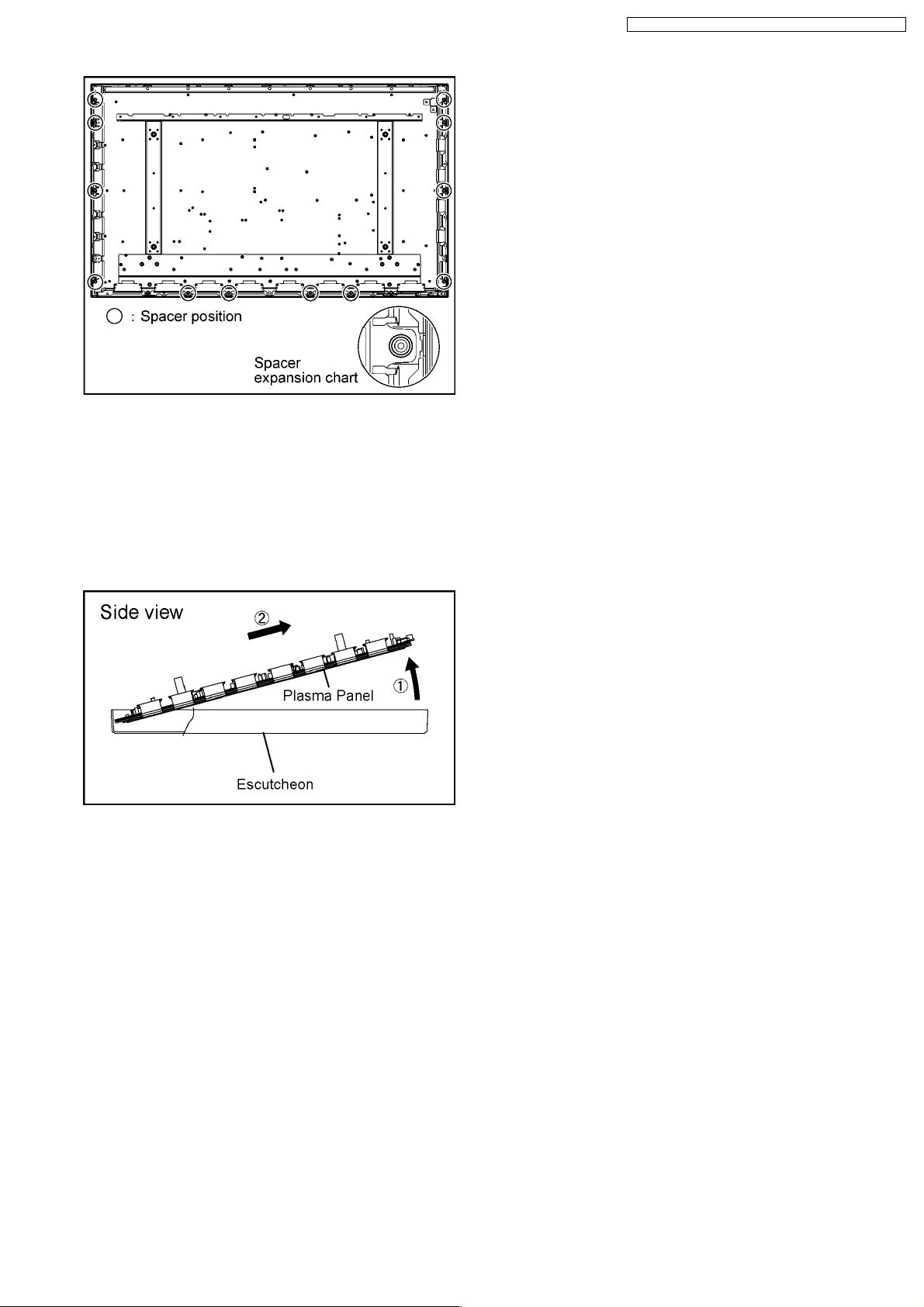
Caution:
·Please confirm the installation place of Spacer and
Spacer Ring when you exchange the Plasma Panel,
and install Spacer and Spacer Ring in an original
installation place after exchanging the Plasma
Panel.
26. Lift up the bottom of the Plasma Panel in the direction of the
arrow 1 and pull the Plasma Panel in the direction of the
arrow 2 and then remove the Plasma Panel.
TH-42PH10BK / TH-42PH10BS / TH-42PH10EK / TH-42PH10ES
17
TH-42PH10BK / TH-42PH10BS / TH-42PH10EK / TH-42PH10ES
7 Location Lead Wiring
7.1. Lead Wiring (1)
The lead wiring is dressed as shown in figure.
18
7.2. Lead wiring (2)
The lead wiring is dressed as shown in figure.
TH-42PH10BK / TH-42PH10BS / TH-42PH10EK / TH-42PH10ES
7.3. Lead wiring (3)
The lead wiring is dressed as shown in figure.
19
TH-42PH10BK / TH-42PH10BS / TH-42PH10EK / TH-42PH10ES
7.4. Lead Wiring (4)
The lead wiring is dressed as shown in figure.
20
8 Adjustment Procedure
TH-42PH10BK / TH-42PH10BS / TH-42PH10EK / TH-42PH10ES
8.1. Driver Set-up
8.1.1. Item / Preparation
1. Set Aging pattern 0 (Vset ajustment pattern) by IIC mode.
2. Set the picture controls as follows.
Picture menu: Standard
Picture: +25
Aspect: Full
Caution
1. First perform Vsus adjustment.
2. Confirmation of Vscn voltage should be performed after
confirmation of Vad adjustment.
When Vad=-105V, Voltage of Vscn is 40V ±4V.
8.1.2. Adjustments
Adjust driver section voltages. (Refer to the panel data on the
panel data label).
Check or adjust the following voltages with the multimeter.
Name Test Point Voltage Volume Remarks
Vsus TPVSUS
(SS)
Ve TPVE (SS) Ve ± 1V VR6000 (SS) *
Vset TPVSET
(SC)
Vad TPVAD (SC) -105V ± 1V VR6600 (SC)
Vscn TPVSCN
(SC)
Vda TPVDA (SS) 75V + 1V, -2V Fixed
PFC C446 (+)(-) 396V ± 0.5V R443 (P)
*See the Panel label.
Vsus ± 2V R628 (P) *
330V ± 7V Fixed
Vad+145V ±4VFixed
21
TH-42PH10BK / TH-42PH10BS / TH-42PH10EK / TH-42PH10ES
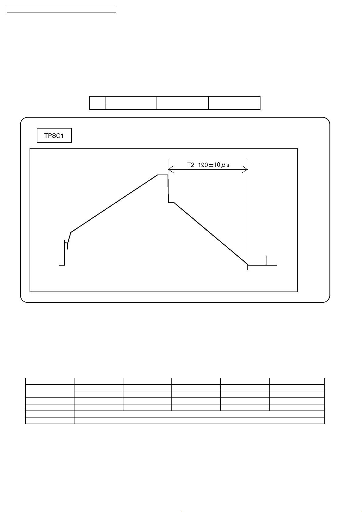
8.2. Initialization Pulse Adjust
1. Set Aging pattern 0 (Vset ajustment pattern) by IIC mode.
2. Set the picture controls as follows.
Picture menu: Standard
Picture: +25
Aspect: Full
3. Connect Oscilloscope to TPSC1 (T2) and adjust VR6602 for 190±10µ Sec.
Test point Volume Level
T2 TPSC1 (SC) VR6602 (SC) 190 ± 10µ Sec.
8.3. P.C.B. (Printed Circuit Board) exchange
8.3.1. Caution
1. To remove P.C.B., wait 1 minute after power was off for discharge from electrolysis capacitors.
8.3.2. Quick adjustment after P.C.B. exchange
Adjust the following voltages with the multimeter.
P.C.B. Name Test Point Voltage Volume Remarks
P Board Vsus TPVSUS (SS) Vsus ± 2V R628 (P) *
PFC C446 (+) (-) (P) 396V ± 0.5V R443 (P)
SC Board Vad TPVAD (SC) -105V ± 1V VR6600 (SC)
SS Board Ve TPVE (SS) Ve ± 1V VR6000 (SS) *
D, DS, DN Board White balance, Pedestal and Sub brightness for NTSC, PAL, HD, PC and 625i signals
DN Board Set Market Select Number to correct destination by MS mode. (See chap. 10.1.4)
*See the Panel label.
Caution:
Absolutely do not reduce Vsus voltage below Ve not to damage the P.C.B.
22
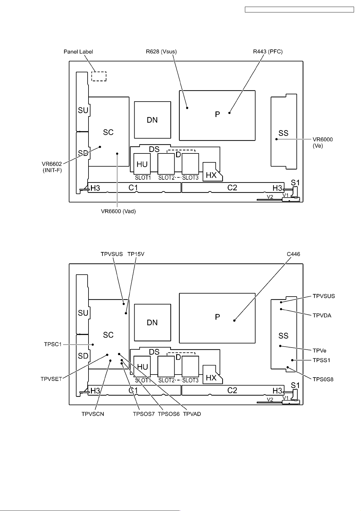
8.4. Adjustment Volume Location
TH-42PH10BK / TH-42PH10BS / TH-42PH10EK / TH-42PH10ES
8.5. Test Point Location
23
TH-42PH10BK / TH-42PH10BS / TH-42PH10EK / TH-42PH10ES
9 Service mode
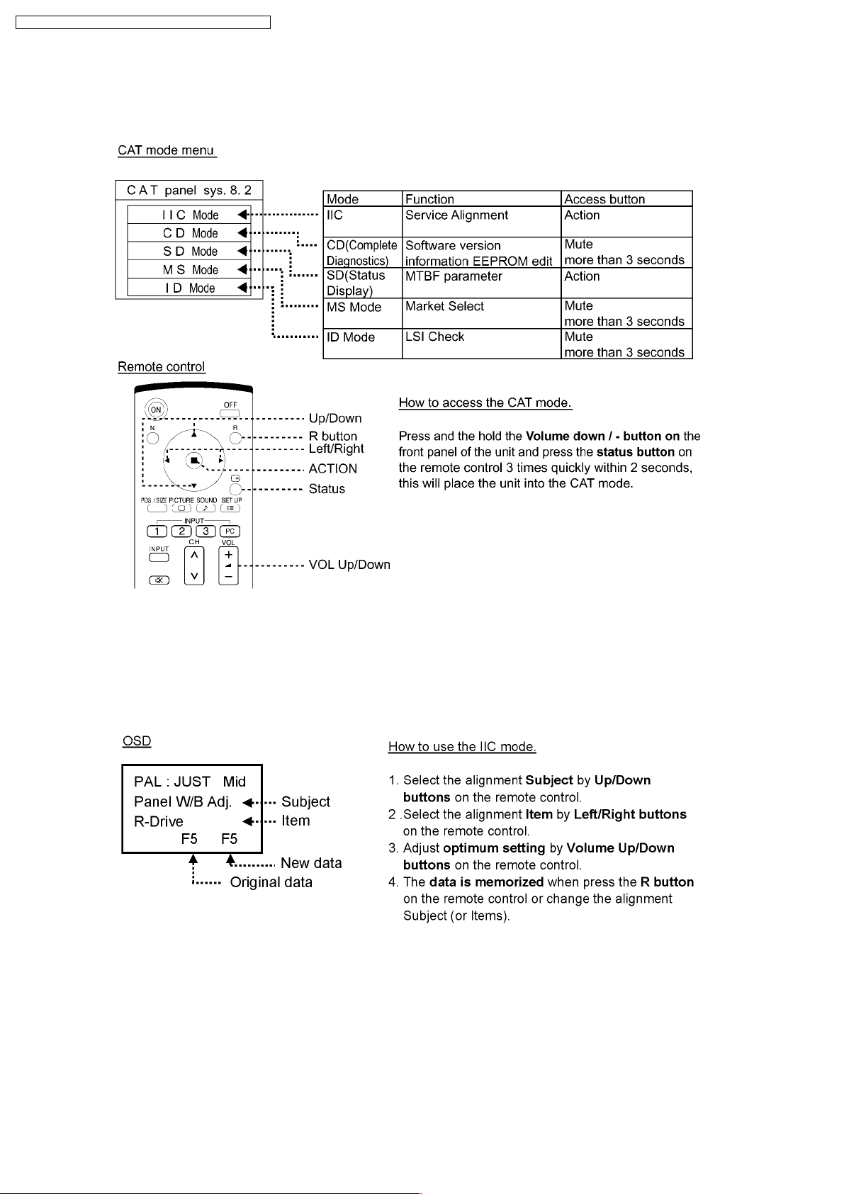
9.1. CAT (computer Aided Test) mode
To exit the CAT mode, access the ID mode and switch off the main power.
9.1.1. IIC mode
Select the IIC mode by Up/Down button on the remote control at the front page of CAT mode and then press the Action button
on the remote control.
Subject and item are mentioned on “IIC mode structure”.
To exit the IIC mode, press the R button on the remote control.
24
TH-42PH10BK / TH-42PH10BS / TH-42PH10EK / TH-42PH10ES
9.1.2. CD mode
Select the CD mode by Up/Down button on the remote control at the front page of CAT mode and then press the Mute button
on the remote control more than 3 seconds.
Microcomputer software version (IC4702), this version can be upgrade by
1. replace of new version IC
2. Loading the new version software from loader tool, TZSC07036.
Memory data change
To exit the CD mode, press the R button on the remote control.
9.1.3. SD mode
Select the SD mode by Up/Down button on the remote control at the front page of CAT mode and then press the Action button
on the remote control.
To exit the SD mode, press the R button on the remote control.
25
TH-42PH10BK / TH-42PH10BS / TH-42PH10EK / TH-42PH10ES
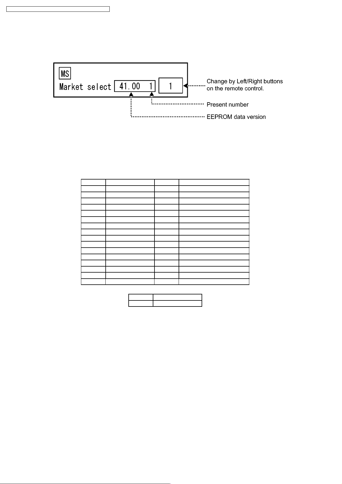
9.1.4. MS mode
Select the MS mode by Up/Down button on the remote control at the front page of CAT mode and then press the Mute button
on the remote control more than 3 seconds.
To exit the MS mode, press the R button on the remote control.
Caution:
Market Select should be set after exchange of DN-Board.
Destination number
Number Destination Number Destination
0 Japan 16 -1 North America 17 -2 Europe 18 China
3 Others 19 China (Hotel)
4 Britain 20 Russia
5 Taiwan 21 Russia (Hotel)
6 Thailand 22 Hong Kong
7 -- 23 -8 Japan (Hotel) 24 --
9 North America (Hotel) 25 -10 Europe (Hotel) 26 -11 -- 27 -12 Britain (Hotel) 28 Middle East/Hong Kong
13 -- 29 Middle East/Hong Kong (Hotel)
14 Thailand (Hotel) 30 Australia
15 -- 31 Australia (Hotel)
Number Destination
Default setting
1 North America
9.1.5. ID mode
Select the ID mode by Up/Down button on the remote control at the front page of CAT mode and then press the Mute button on
the remote control more than 3 seconds.
26
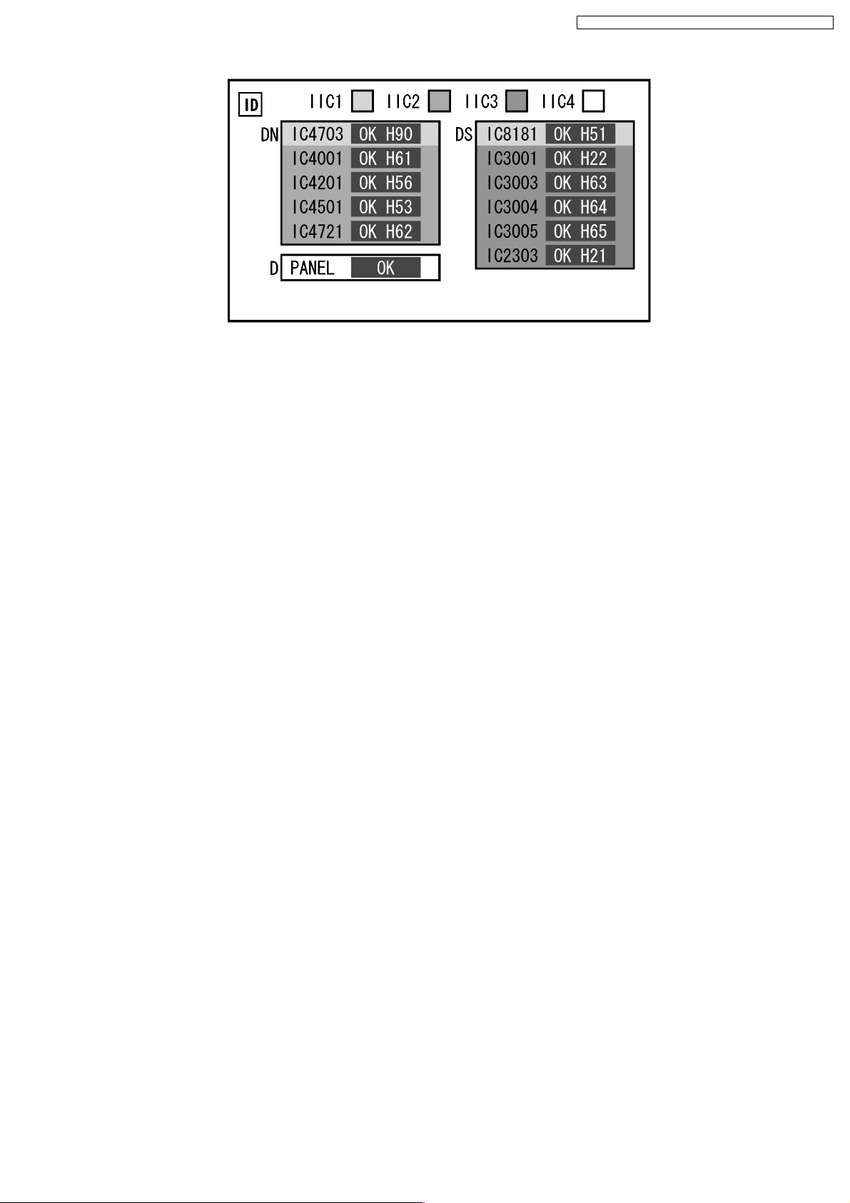
To exit the ID mode, press the R button on the remote control.
TH-42PH10BK / TH-42PH10BS / TH-42PH10EK / TH-42PH10ES
27
TH-42PH10BK / TH-42PH10BS / TH-42PH10EK / TH-42PH10ES
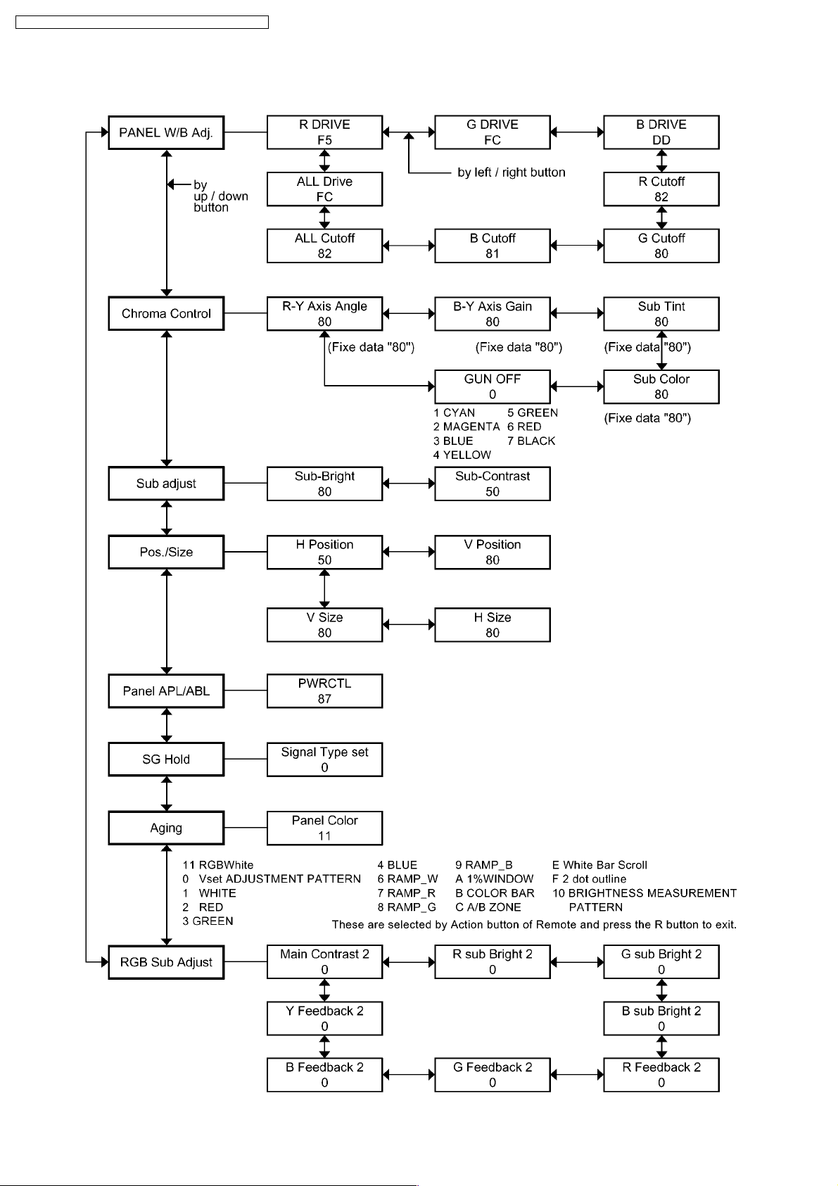
9.2. IIC mode structure (following items value is sample data.)
28
10 Adjustment
10.1. RGB white balance adjustment
Instrument Name Connection Remarks
· RGB VGA W/B pattern
· Color analyzer
(Minolta CA-100 or equivalent)
Procedure Remarks
· Ensure aging is adequate.
· Make sure the front panel to be used on the final set is fitted.
· Make sure a color signal is not being shown before adjustment.
· Put the color analyzer where there is little color variation.
1. Set COMPONET/RGB-IN SELECT to RGB.
2. Select the IIC mode “PANEL W/B Adj.” item.
3. Check that the color temperature is “COOL (High)”.
4. Output a white balance pattern.
5. Touch the signal receiver of color analyzer to the highlight window’s center.
6. Fix G drive at E0h and adjust B drive and R drive so x, y become the “Color temperature
High” in the below table.
7. Increase R/G/B together so the maximum drive value in R/G/B becomes FCh.
8. Set color temperature to “NORMAL (Medium)”.
9. Fix G drive at E0h and adjust B drive and R drive so the highlight window’s x, y becomes
the “Color temperature Medium” in the below table.
10. Increase R/G/B together so the maximum drive value in R/G/B becomes FCh.
11. Set color temperature to “WARM(Low)”.
12. Set G drive to E0h and adjust B drive and R drive so the highlight window’s x, y become
the “Color temperature Low” shown in the below table.
13. Increase R/G/B together so the maximum drive value in R/G/B becomes FCh.
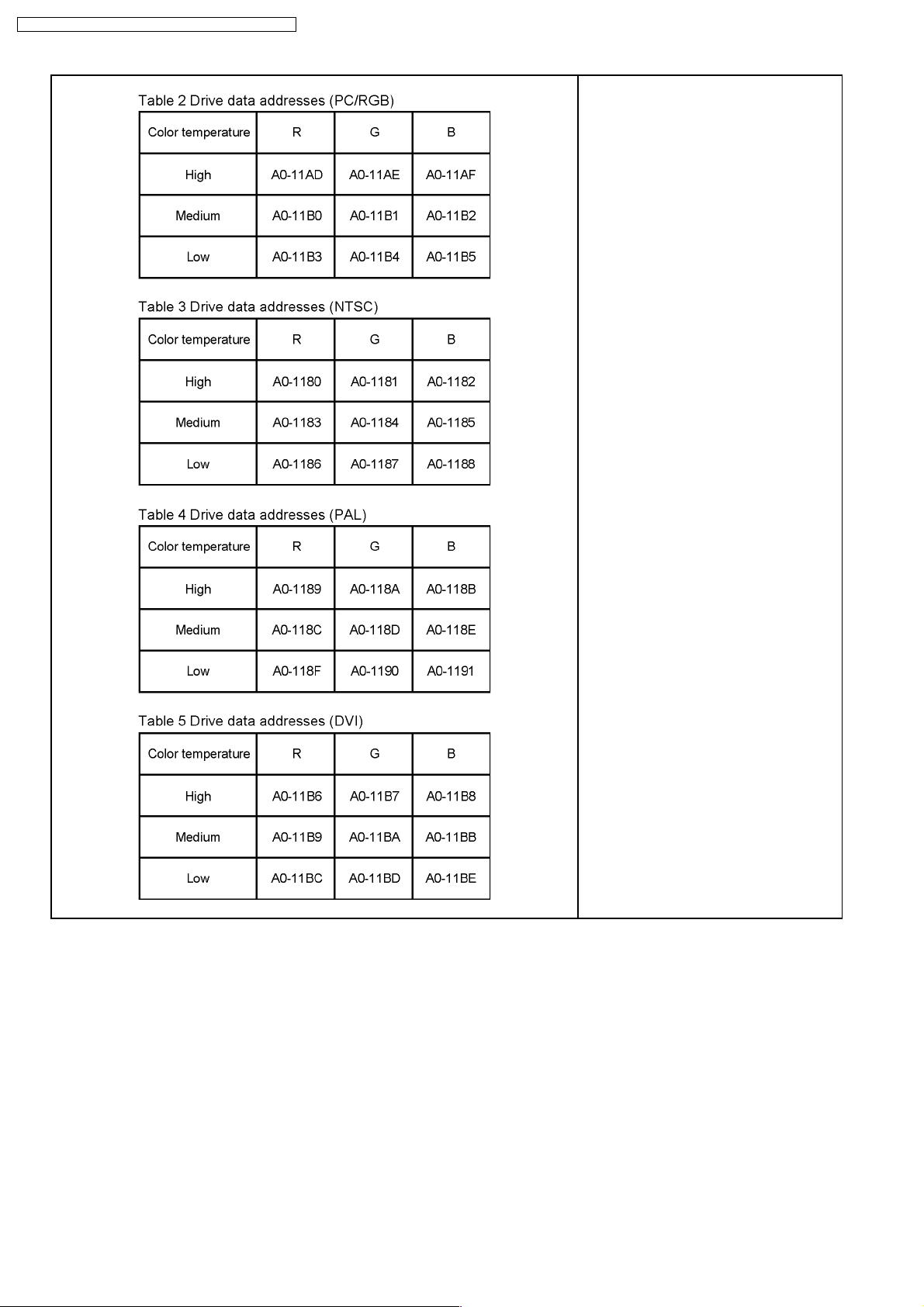
14. Copy the R drive, G drive and B drive data in NTSC, PAL DVI region.
PC input
Panel surface
TH-42PH10BK / TH-42PH10BS / TH-42PH10EK / TH-42PH10ES
User setting: Normal
(Picture menu: Standard)
Picture Menu: Standard
Picture: 25
Aspect: Full
Position and size: Normal
· Highlight section Signal amplitude 75%
· Cutoff standard G: 80h
· Drive standard G: E0h
Adjustment target
Hi-light: x ± 0.003 y ± 0.003
Hi-light is target of the number at drive adjustment in the hi-light windows.
Therefore, it is not target of the hi-light number at after adjustment white balance.
29
TH-42PH10BK / TH-42PH10BS / TH-42PH10EK / TH-42PH10ES
30
 Loading...