

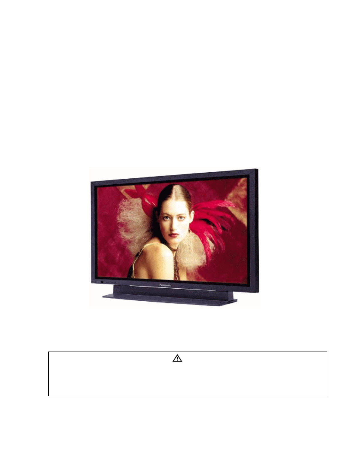
Panasonic TH-42PH Service Manual
Panasonic Services Company
National Training
TH-42PHD5/TH-50PHD5
TH-42PHW5/TH50PHW5
GPH5D Chassis
Plasma Display Panel
Troubleshooting Guide
This service information is designed for experienced repair technicians only and is not designed for use by the general public. It does
not contain warnings or cautions to advise non-technical individuals of potential dangers in attempting to service a product. Products
powered by electricity should be serviced or repaired only by experienced professional technicians. Any attempt to service or repair
the product or products dealt with in this service information by anyone else could result in serious injury or death.
Warning

2

Objective...............................................................................................................5
2002 Model Line Up..............................................................................................6
Specifications.....................................................................................................7
Features.............................................................................................................8
New Asymmetrical Cell Structure Panel .........................................................9
Model Differences...........................................................................................9
Disassembly .......................................................................................................11
Rear Cover Removal .......................................................................................11
42” HD PCB Board Layout Diagram ...................................................................13
Printed Circuit Board Information Table ...........................................................13
50” PCB Board Layout Diagram .........................................................................14
42” SD PCB Layout Diagram..............................................................................15
Video Signal Path Explanation............................................................................16
HY/HZ Board....................................................................................................16
HX Board .........................................................................................................17
D1 Board..........................................................................................................18
DVI Interface....................................................................................................19
Sync Process...................................................................................................21
RGB/PC Input Mode Sync ...............................................................................21
Composite/ Component Video Input mode Sync .............................................21
D1 Board.............................................................................................................22
D1 Main ICs Operation ....................................................................................22
D2 Board.............................................................................................................23
D2 Board details ..............................................................................................24
SC Board Explanation.........................................................................................25
SS Board Explanation.........................................................................................28
Power Supplies...................................................................................................31
Standby Power Supply.....................................................................................31
Main Power Supply..........................................................................................32
Power Factor Control....................................................................................32
Low Voltage Power supply............................................................................33
Voltage Regulation........................................................................................33
High Voltage Power Supply .............................................................................34
Protection Circuits...............................................................................................36
Diagnostic Procedures........................................................................................38
Self Check Display Indication...........................................................................38
Power LED Flashing timing chart.....................................................................39
Diagnostic Flow Charts.......................................................................................40
No Power .........................................................................................................40
The Power LED is red and blinking on/off........................................................41
Power LED blinks twice ...................................................................................42
No Picture Flowchart 1.....................................................................................43
No picture Flowchart 2.....................................................................................44
Dark picture Flowchart.....................................................................................45
Local screen failure.............................................................................................46
3

Service Hints....................................................................................................46
After Image Prevention .......................................................................................53
Screen Saver Feature...................................................................................53
Side Bar Brightness adjustment....................................................................54
Option Setting .....................................................................................................55
Accessing the Option Menu.............................................................................55
Hidden Option Menu for GPH5D series...........................................................56
Sample Waveforms.............................................................................................58
HY/HZ board....................................................................................................58
HX board..........................................................................................................61
SC Board Input Signals....................................................................................63
SC Board Waveforms ......................................................................................64
SS-Board Input Signals....................................................................................66
SS Board Waveforms ......................................................................................67
PDP Defect Pixel Specification ...........................................................................68
Connector Tables................................................................................................69
F-BOARD CONNECTORS ..............................................................................69
P-BOARD CONNECTORS ..............................................................................69
HX- BOARD CONNECTORS...........................................................................73
HY / HZ- BOARD CONNECTORS...................................................................74
Adjustment Procedures.......................................................................................75
Panel label Information ....................................................................................75
+B Set-up.........................................................................................................76
Confirmation.....................................................................................................76
Driver Set-up....................................................................................................77
Initialization Pulse Adjust .................................................................................78
P.C.B. (Printed Circuit Board) exchange procedure.........................................79
Adjustment Volume Locations..........................................................................79
Test Point locations..........................................................................................80
Serviceman mode...............................................................................................81
CAT (computer aided test) Mode.....................................................................81
I2C Mode..........................................................................................................81
CD mode..........................................................................................................82
SD Mode..........................................................................................................83
2
C Menu Structure ..........................................................................................84
I
Alignment Procedures.........................................................................................85
NTSC Panel White Balance............................... Error! Bookmark not defined.
Pedestal Setting...............................................................................................85
NTSC (480i) White Balance Adjustment ..........................................................86
480p White Balance Adjustment......................................................................87
720p White Balance Adjustment......................................................................88
1080i White Balance Adjustment.....................................................................89
Sub Brightness Setting ....................................................................................90
Service Contact Information................................................................................91
4

Objective
The information provided in this document is designed to assist the technician in
determining the defective printed circuit board. The troubleshooting flow charts,
signal path charts and connector information should provide enough detail that
the technician can accurately determine which one of the printed circuit boards is
required to repair the product. Alignment and adjustment procedures are also
included in this document.
The Block diagrams and the schematic drawings reference the model TH42PHD5, but the technology is consistent with any GPH5D chassis.
5
2002 Model Line Up
Digital Cinema Reality
Advanced 3-dimensional
1366 x 768 XGA Resolution
TH-50PHW5
50-inch (127 cm)
Wide Plasma Display
Plasma Contrast Automatic
Tracking System (C.A.T.S.)
3-Dimensional Progressive
VGA Resolution (UXGA
TH-42PW5
42-inch (106 cm)
HD Plasma Display
HD Panel
Progressive Scan
(UXGA Compatible)
Scan
Compatible)
TH-42PHW5
42-inch (106cm)
TH-37PW5
37-inch (94cm)
6
Specifications
Our New 50” & 42” HD Progressive Panels
The industry’s highest-resolution panels
Panasonic Company PI Company F/H
Scanning Method Progressive Progressive
50-
inch
1,366 x 768=
1.05 million pixels
1,280 x 768=
0.98 million pixels
Interlace
N/A
Pixel
pitch
42/43-
inch
Pixel
pitch
Relationship between Picture resolution and Scanning method: 768p > 720p >
680p = 1080i > 1024i
0.810 (H) x 0.810 (V)
= 0.656
(42” Screen size)
1,024 x 768=
0.79 million pixels
0.898 (H) x 0.674 (V)
= 0.605
0.858 (H) x 0.808 (V)
= 0.693
(43” Screen size)
1,024 x 768=
0.79 million pixels
0.930 (H) x 0.698 (V)
= 0.649
(42” Screen size)
1,024 x 512=
0.52 million pixels
0.90 (H) x 1.02 (V)=
0.918 / 2= 0.459
[1frame]
7
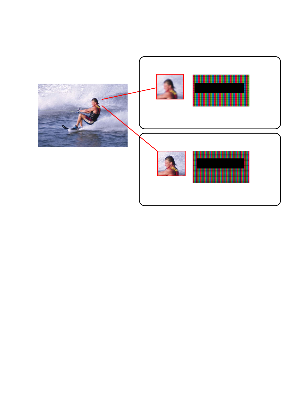
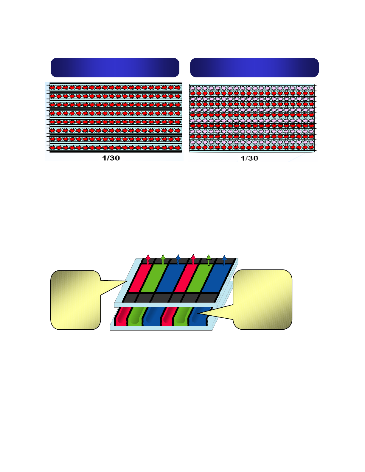
Features
Pixel explanation
SD (Standard Definition) Panel
852 pixels
410,000 Pixels
Provides the optimum number of pixels for viewing
standard broadcasts and DVD.
480 pixels
HD (High-Definition) panel
1,024 pixels
768 pixels
790,000 pixels
Reproduces even the tiniest details of high-definition
sources and other high-quality images.
Figure 1
8
Scan Explanation
Panasonic progressive scan ALIS system Interlace scan
Figure 2
The 1-field (1/60 sec) display pixels on the Panasonic 42" and 37" SD models
and on the ALIS system models are VGA level. (Panasonic HD models are XGA
level, for higher resolution.)
A.L.I.S. (Alternate Lighting of Surfaces) method is one of the new panel driving
systems of plasma display developed by Fujitsu Limited. ALIS method is a
system developed from the 3 electrode discharging system.
The ALIS method uses an interlaced driving scheme, which means the even and
odd lines are addressed alternately.
New front
protection
filter glass
improves
the natural
reds
New
phosphors
improve the
blue color
reproduction.
•
Figure 3
New Asymmetrical Cell Structure Panel
Figure 3 shows the unique asymmetrical cell structure that achieves both high
brightness and crisp whites. The asymmetrical arrangement of the red, blue and
green cells that control color reproduction results in a dramatically improved lightemitting balance of the three primary colors. This reproduces purer whites while
maintaining a high level of brightness.
Model Differences
9
SSiinnggllee SSccaann ((SSDD))
DDuuaall SSccaann ((HHDD))
Figure 4
•Simple and low cost circuit •High performance
•Higher brightness
10
Figure 5
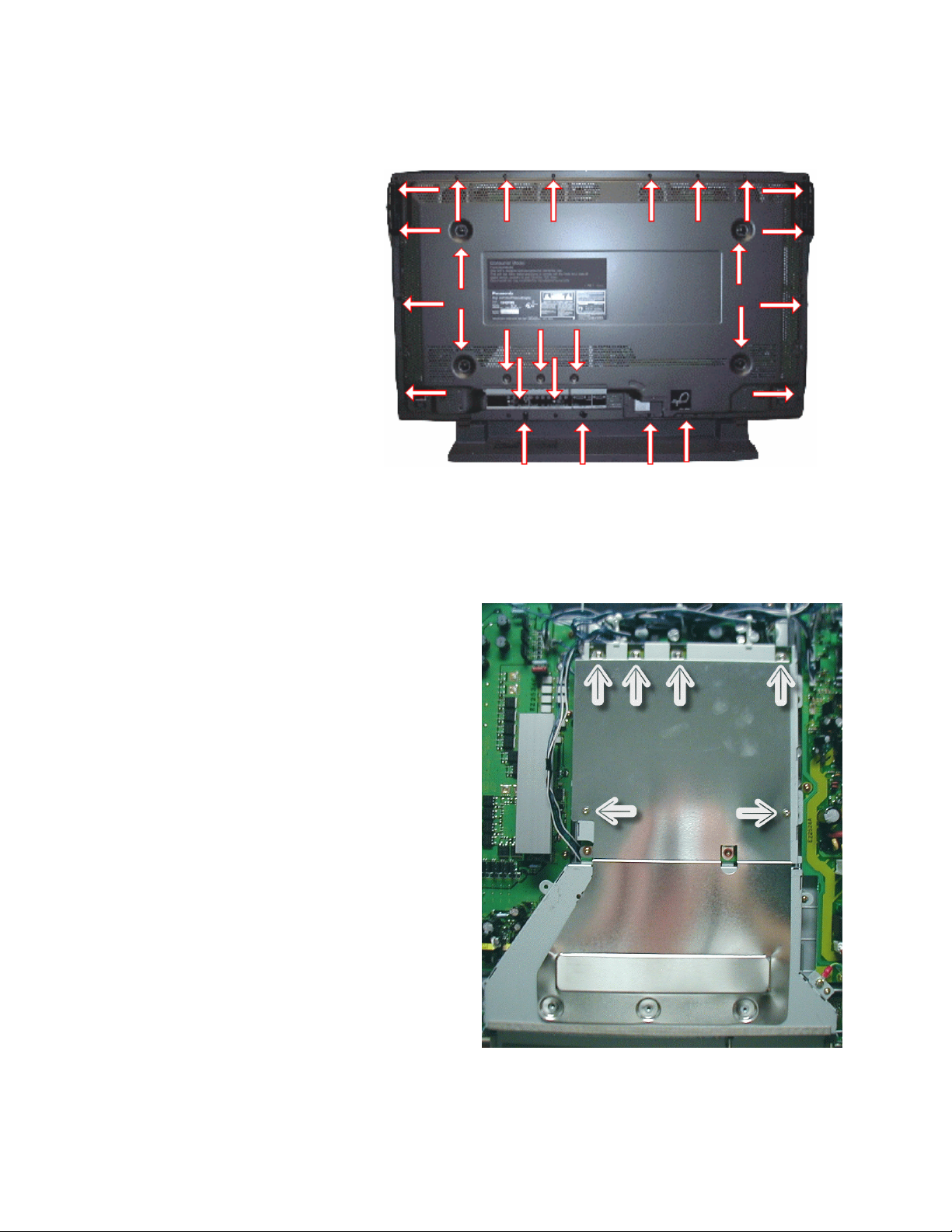
Disassembly
Rear Cover Removal
Remove the 27 screws,
shown in Figure 6, and
then pull away the rear
cover.
Removal of the shield
Remove the six screws, shown in
Figure 7, and then pull away the rear
shield cover.
Figure 6
11
Figure 8
Figure 7
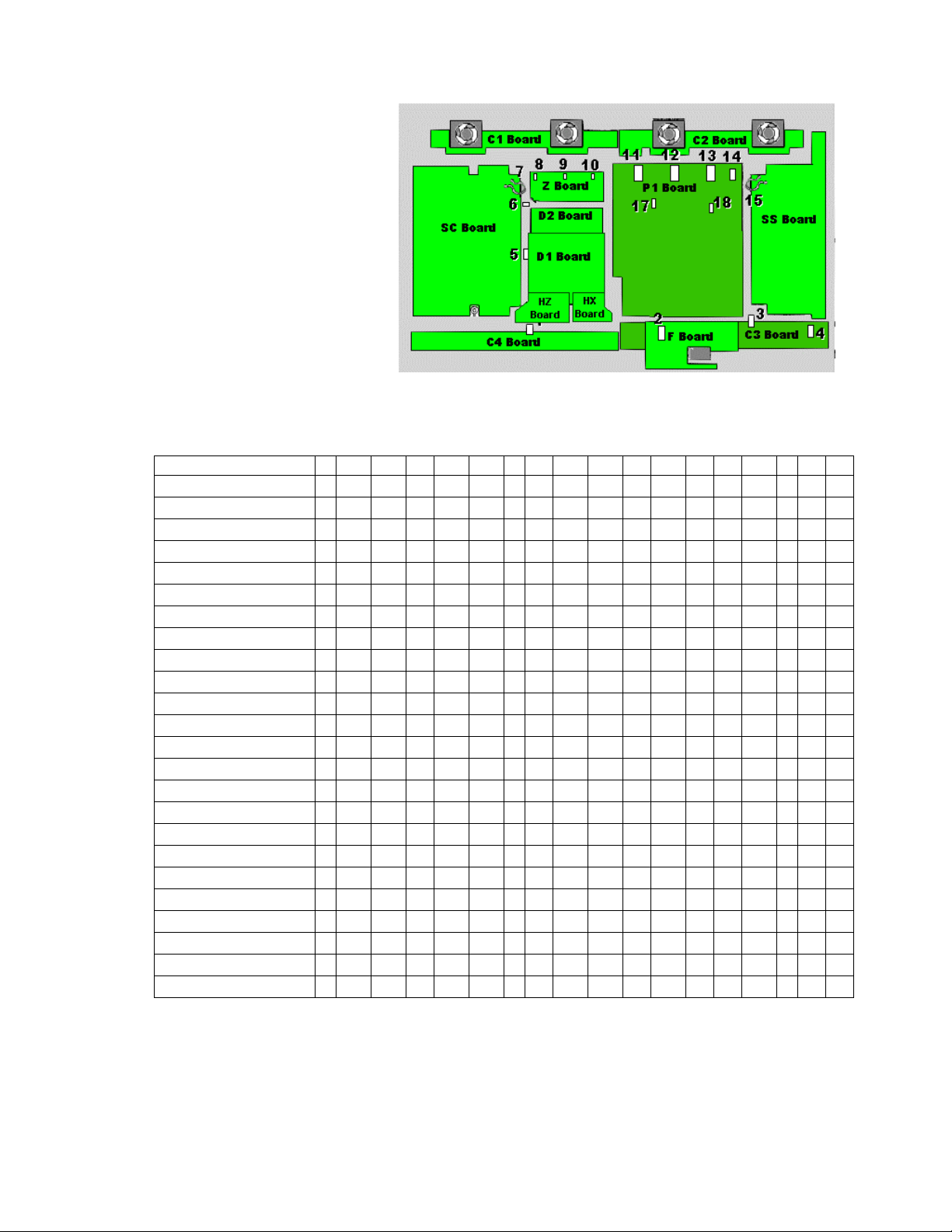
Location of Lead Wiring
High frequency
electromagnetic signals can
create electrical interference
within the unit. Be sure to
route all wires through their
respective harnesses
reference.
The chart below is an
illustration representing the
connectors and the wire
harnesses associated
Clamper Locations
Figure 9
with them.
Harness Number
Connector Number 1 2 3 4 5 6 7 8 9 10 11 12 13 14 15 16 17 18
Z6 P6
Z10 D10
Z17 D17
D12 D22
D16 D26
D25 P5
D27 P7
SC2 P2
SC4 P4
SC20 D20
SC21 D21
H37 Z3
H37 Z4
SS1 P1
SS3 P3
SS32 C32
SS42 C42
ESC POWER SS34
ESC V-BOARD C44
F9 P9
Fan 1 P10
Fan 2 P11
Fan 3 P12
Fan 4 P13
= Wind the cable through the clamper once
= Wind the cable through the clamper two times
= Wind the cable through the clamper three times
12
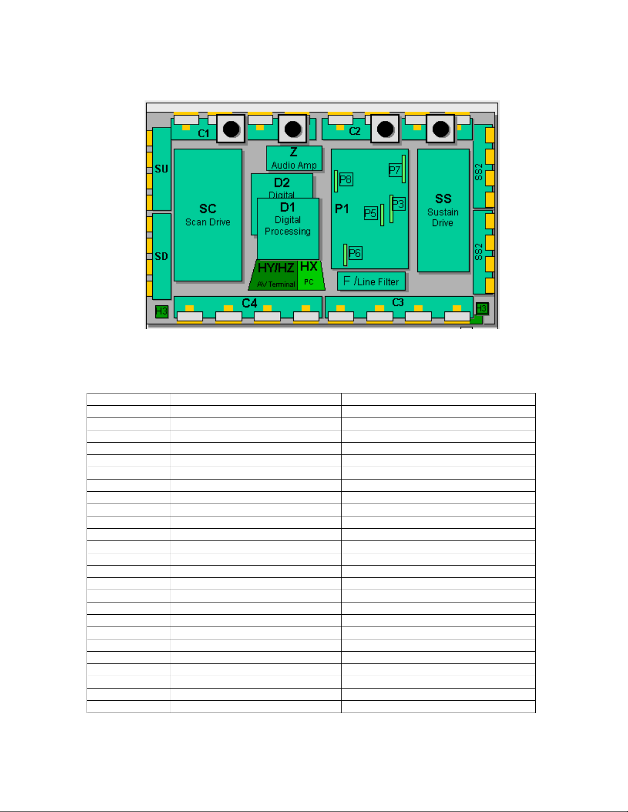
42” HD PCB Board Layout Diagram
Figure 10
Printed Circuit Board Information Table
Board Name Part Number Function
C1 TNPA2428 Data Drive (Upper Left)
C2 TNPA2429 Data Drive (Upper Right)
C3 TNPA2430 Data Drive (Lower Right)
C4 TNPA2431 Data Drive (Lower Left)
D1 TZTNP01LLSB Format Converter
D2 TNPA2427 Plasma AI Sub-Field Processor
F TNPA2444 Line filter
H3 TNPA2249 Speaker terminal
HX TZTNP01LLSU PC type Input terminal
HZ TXNHZ40JJS RCA type Input terminal
P TXN/P10LLS Power supply
P3 TNPA2439 Drive voltage oscillator
P5 TNPA2440 Primary oscillator
P6 TNPA2441 PFC oscillator
P7 TNPA2442 Drive voltage protection
P8 TNPA2443 Process voltage protection
S1 TNPA2283AC Power switch
SC TNPA2434 Scan out
SD TNPA2433 Scan connection (Lower)
SS TNPA2435 Sustain out
SS2 TNPA2436 Sustain connection (Upper)
SS3 TNPA2437 Sustain connection (Lower)
SU TNPA2432 Scan connection (Upper)
V1 TNPA2282AC Front SW. & Remote receiver
Z TNPA2445 Audio out
13
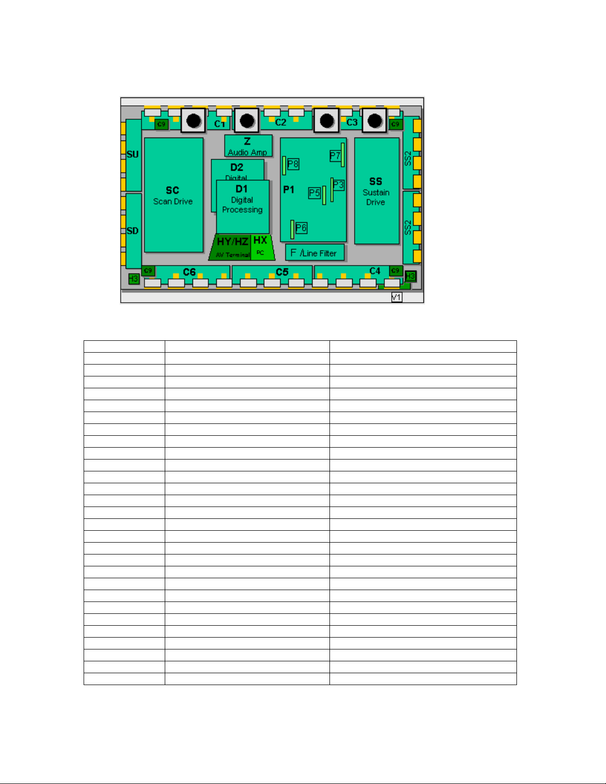
50” PCB Board Layout Diagram
Board Name Part Number Function
C1 TNPA2510 Data Drive (Upper Left)
C2 TNPA2511 Data Drive (Upper Center)
C3 TNPA2512 Data Drive (Upper Right)
C4 TNPA2513 Data Drive (Lower Right)
C5 TNPA2514AB Data Drive (Lower Center)
C6 TNPA2515 Data Drive (Lower Left)
C9 TNPA2608 Energy Recovery Circuit
D1 TZTNP01MHSB Format Converter
D2 TNPA2427AB Plasma AI Sub-Field Processor
F TXN/F10MHS Line filter
H3 TNPA2249 Speaker Terminal
HX TZTNP02KESE PC type Input terminal
HZ TXNHZ40JJS RCA type Input terminal
P1 TXNP110MHS Power supply
P3 TNPA2566 Drive voltage oscillator
P5 TNPA2567 Primary oscillator
P6 TNPA2568 PFC oscillator
P7 TNPA2569 Drive voltage protection
P8 TNPA2570 Process voltage protection
S1 TNPA2283AC Power switch
SC TNPA2434AB Scan out
SD TNPA2518 Scan connection (Lower)
SS TXNSS10MHS Sustain out
SS2 TNPA2519 Sustain connection (Upper)
SS3 TNPA2520 Sustain connection (Lower)
SU TNPA2517 Scan connection (Upper)
V1 TNPA2282AC Front SW. & Remote receiver
Z TNPA2445 Audio out
Figure 11
14
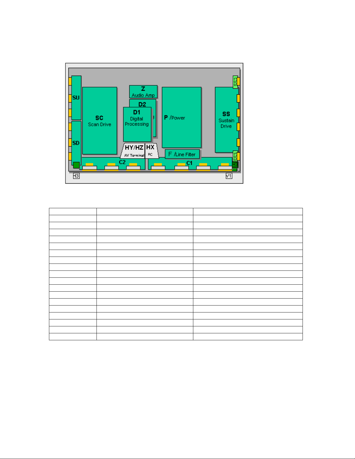
42” SD PCB Layout Diagram
Figure 12
Board Name Part Number Function
C1 TNPA2540 Data Drive (Lower Right)
C2 TNPA2541 Data Drive (Lower Left)
D1 TZTNP01MMSB Format Converter
D2 TNPA2589 Plasma AI Sub-Field Processor
F TXN/F10MMS Line filter
H3 TNPA2249 Speaker terminal
HX TZTNP020JAS PC type Input terminal
HZ TXNHZ40JJS RCA type Input terminal
P TNPA2598 Power supply
S1 TNPA2622 Power switch
SC TNPA2534 Scan out
SD TNPA2584 Scan Connection (Lower)
SS TNPA2535 Sustain Out
SS2 TNPA2536 Sustain Connection (Upper)
SS3 TNPA2537 Sustain Connection (Lower)
SU TNPA2583 Scan Connection (Upper)
V1 TNPA2621 Front SW. & Remote Receiver
Z TNPA2590 Audio out
15
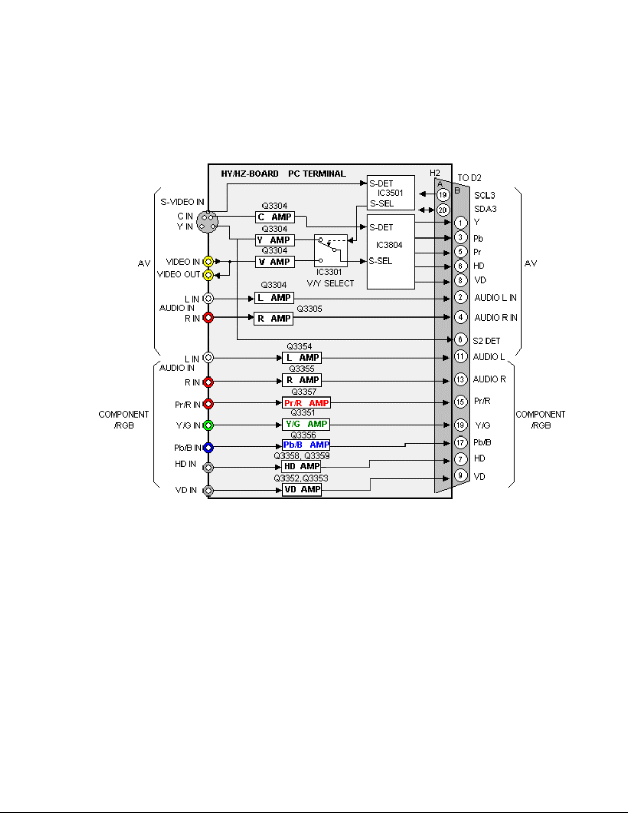
Video Signal Path Explanation
HY/HZ Board
Figure 13
The "HY/ HZ" board is equipped with one Component input, one Composite input
and one S-Video input. The Composite and S-Video inputs are applied to a
switching circuit, which is controlled by the system control IC, located on the D1Board. The switch select command is sent via the SCL3 and SDA3 lines. After
signal selection the composite or S-Video signals are amplified, buffered, and
applied to a 3D comb filter inside IC3803. The 3D Comb filter converts the
Composite input signals to Y, Pb, and Pr component signals. The output of
IC3804 is applied to the D1 Board via pins 1, 3, and 5 of the connector H2/D2.
Individual amplifiers buffered the Component input signals that are then applied
to the D1-Board via pins 15, 17, and 19 of the connector H2/D2. Vertical and
Horizontal Sync signals are also amplified on this board before they are applied
to the D1 Board.
16
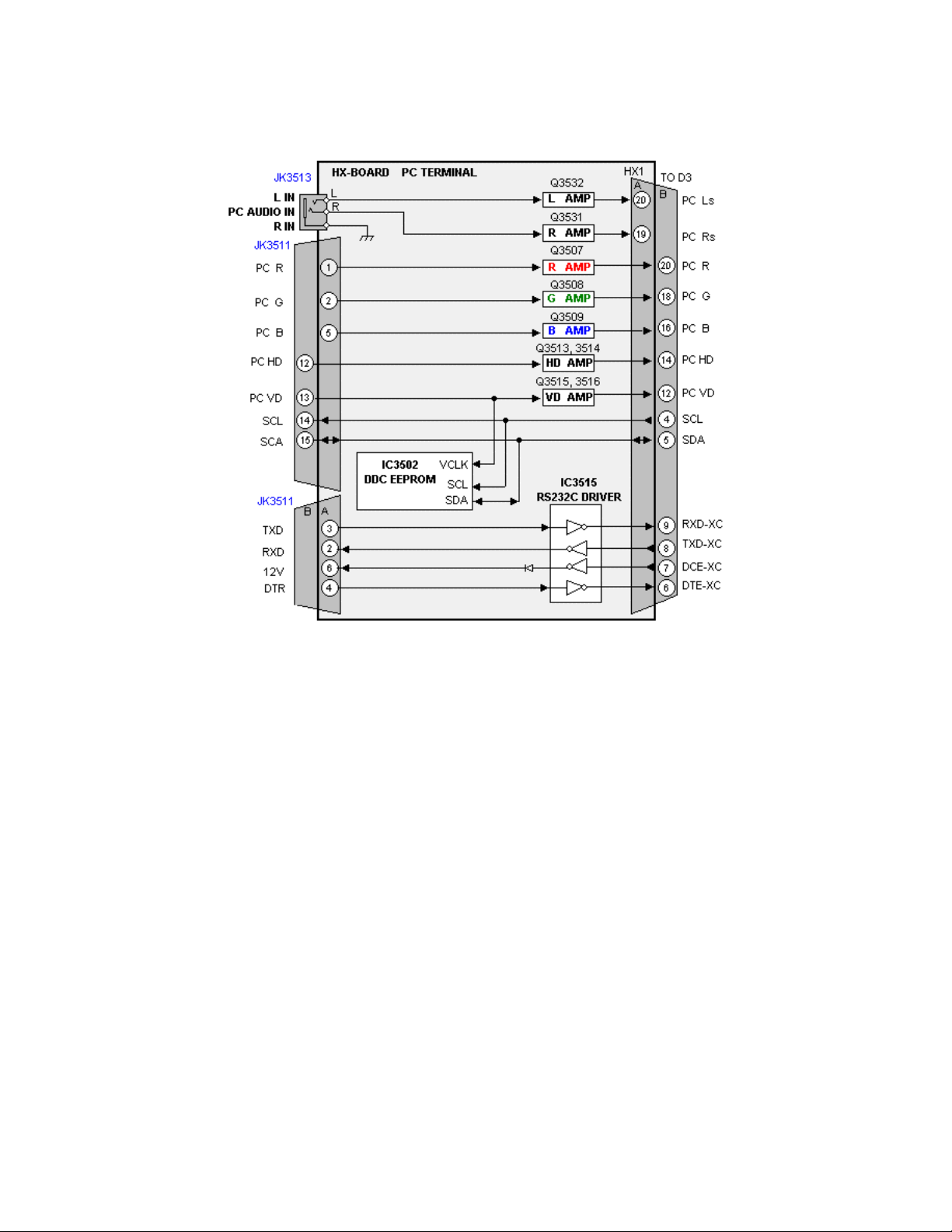
HX Board
Figure 14
PC RGB Signals are input to the HX Board. The RGB signals as well as the
vertical and horizontal sync signals are amplified by a series of transistor
amplifiers. The RS232C communications bus line is also connected on this
board. The RS-232C connection is provided so that operation changes can be
made via PC. An example of an application of this port would be remote turn on
of the unit for a kiosk or similar display.
The outputs of the HX board are applied to the D1 board via connector HX1/D3.
17
D1 Board
Figure 15
After the input signals are amplified by the HY/HZ and HX boards the desired
signal is selected. The microprocessor sends the command via the IIC bus to the
input select switch (IC3001). The video switch selects from one of the three
inputs. The component video signal output from the video switch is amplified and
converted to digital. An optional Digital Visual Interface (DVI) input bypasses the
A/D process as DVI information is already in the digital format.
Concurrently, the desired sync signals are selected and applied to the Sync
Processor. NTSC and Component sync signals are stripped from the Green
video component while the PC sync is applied directly. The Sync Processor
combines the On-Screen Display Sync signal with the input sync and converts
them to match the video format.
The corresponding audio signal is selected by an Audio switch and applied to the
Z board for further amplification
18
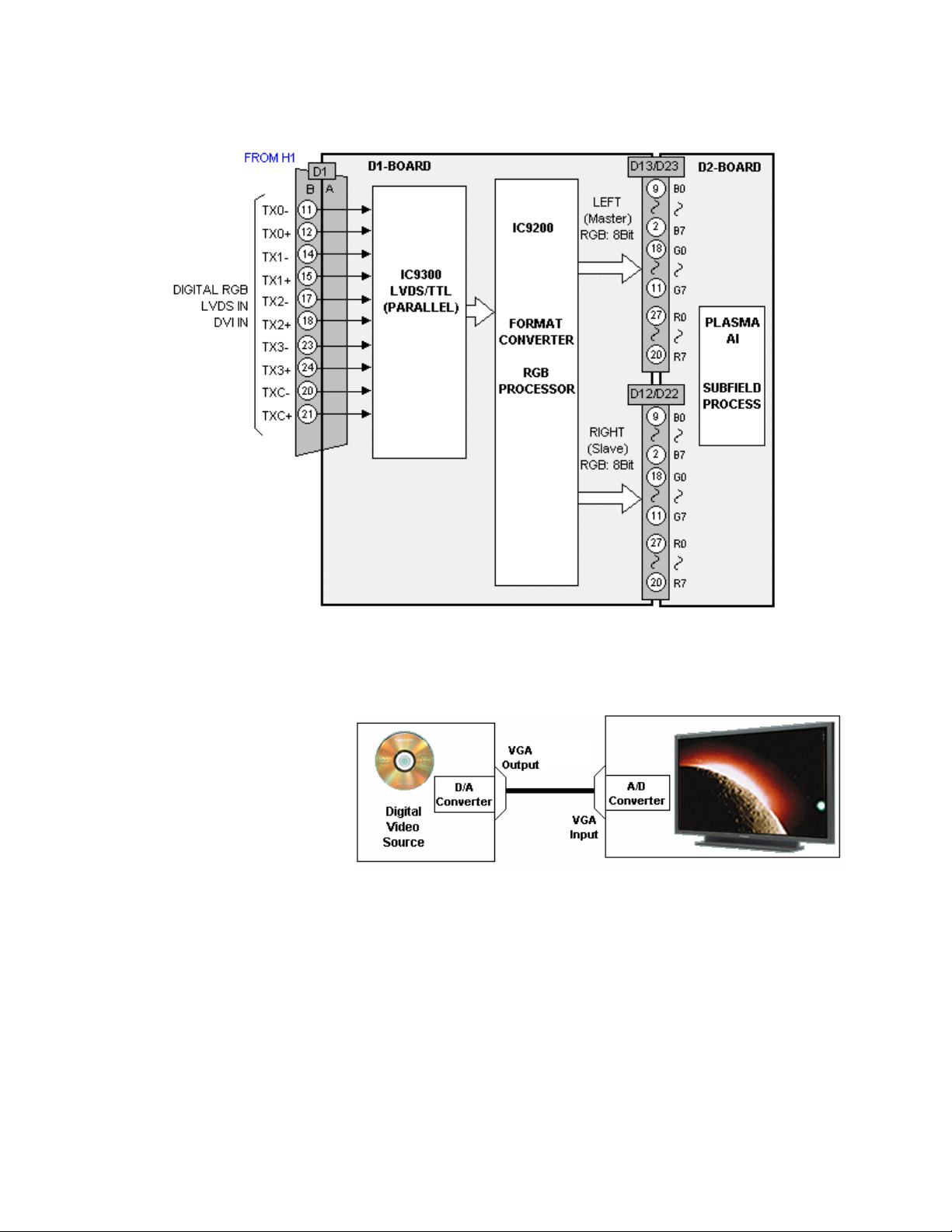
DVI Interface
Figure 16
An optional Digital Visual Interface (DVI) module connection is provided on this
generation Plasma Display Panels. The DVI interface allows direct digital transfer
from a display device to
the panel. A VGA or
component video signal
requires a conversion
from the digital to
analog and then
conversion back to
digital prior to input to
the Format converter see
Figure 17. The double
conversion can introduce
distortion to the signal.
Figure 17
19
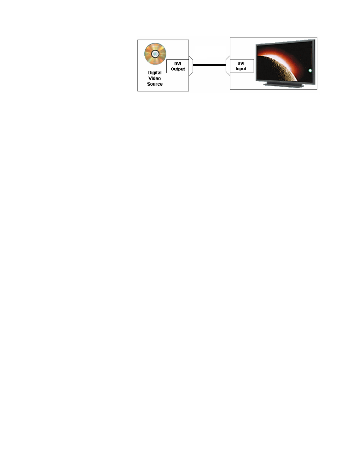
Figure 18 shows an
example of the DVI
interface. It permits direct
connection of the digital
video signal to the Format
converter. This bypasses
the D/A and A/D process
providing the better
quality picture.
Installation of the DVI interface requires removal of the HY/HZ Board and
replacing it with an optional DVI interface board.
Figure 18
20
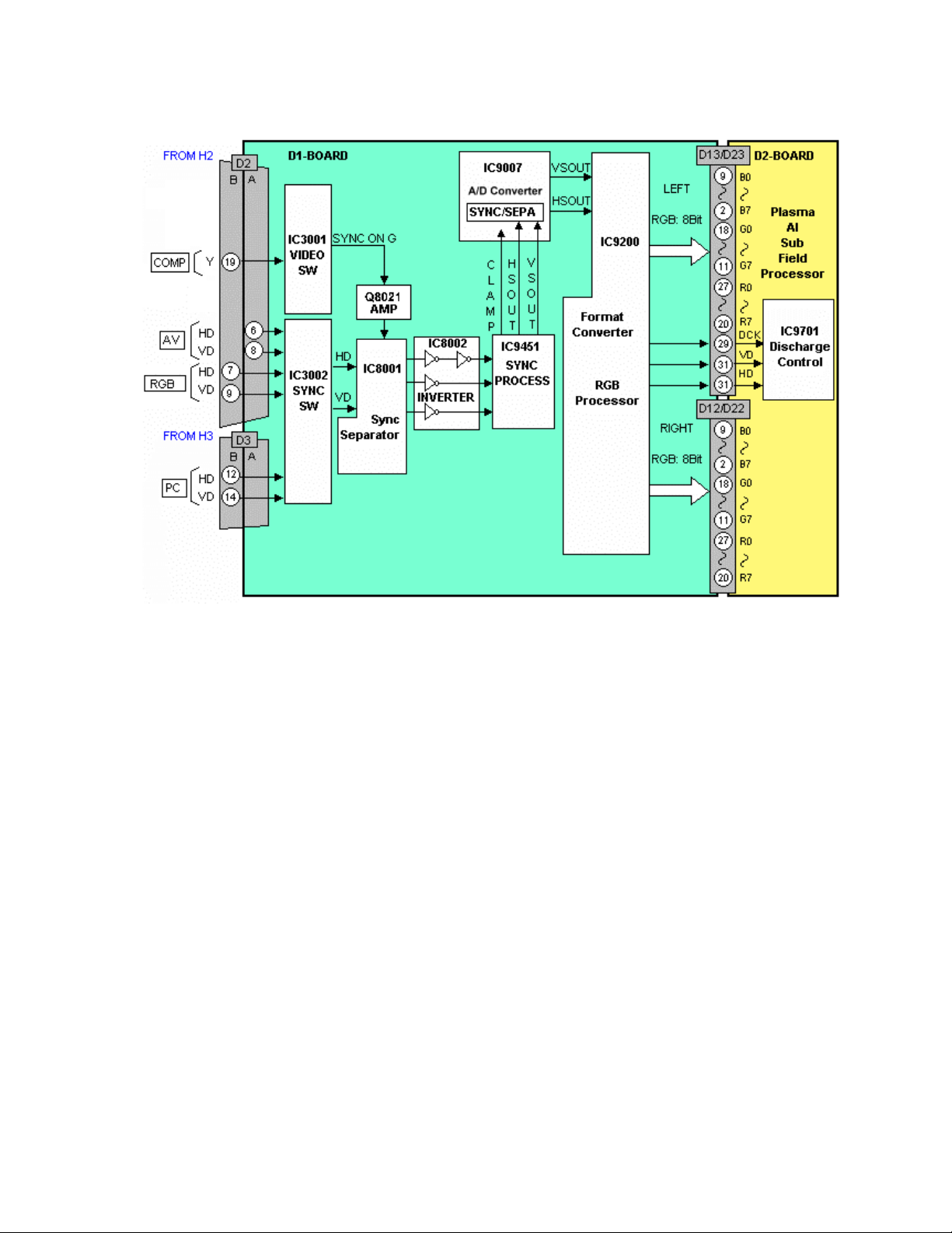
Sync Process
Figure 19
The vertical and horizontal sync signal paths are slightly different depending on
the Source signal.
AV/RGB/PC Input Mode Sync
The vertical and horizontal sync signals generated by the input device are
applied to connector D3 or D2 to a Sync switch (IC3002). IC3002 outputs the
vertical and horizontal sync signals. The signals are inverted by IC8002 and then
applied to a sync processor (IC9451). IC9451 mixes the image sync signal with
the OSD sync signal prior to output to the format converter (IC9200).
Component Video Input mode Sync
The Y video signal is applied to an input switch (IC3001). The Sync on green
signal is amplified by Q8001 and applied to a sync separator (IC8001). IC8001
outputs the Vertical and Horizontal sync signals. From that point on the sync path
is the same as the RGB/PC input mode.
The A/D converter (IC9007) shapes the analog sync signal to clean digital pulses
prior to input to the format converter.
21
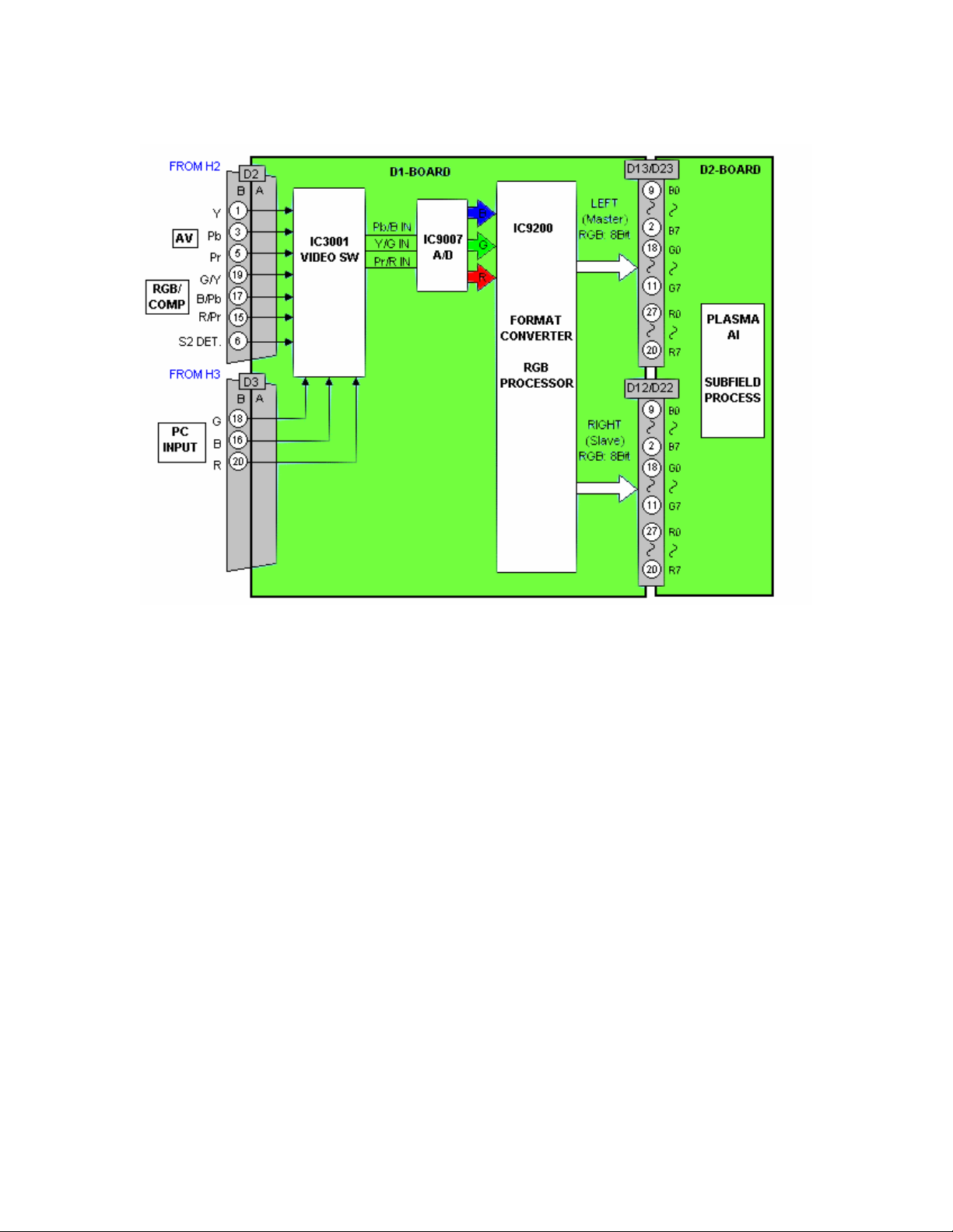
D1 Board
Figure 20
D1-board consists of the Analog and Digital signal process. It also contains the
Discharge control and Microprocessor control block. Supply voltages of 13.5V,
5V, Standby 5V, 3.3V, and 1.8 V operate the D1-board. The input RGB video
signals are at 0.7Vp-p. Video signals in the form of parallel data and the control
signals for the data drive circuit are output.
D1 Main ICs Operation
IC3001 Video Switch
The user selects the desired video input using the front panel button or the
remote control. The microprocessor reads this data and sends out a command
via the IIC bus line. The IIC data is read by IC3001 and the video input is chosen.
IC9007 A/D Converter
This integrated circuit converts the RGB analog signals to eight bit parallel data.
IC9200 Format Converter
The digital video data is converted to progressive scan and mixed with the OSD
data. Other adjustments such as white balance, contrast and color are also
corrected here. The two channels of data are output to the D2 board for the subfield drive circuit.
22
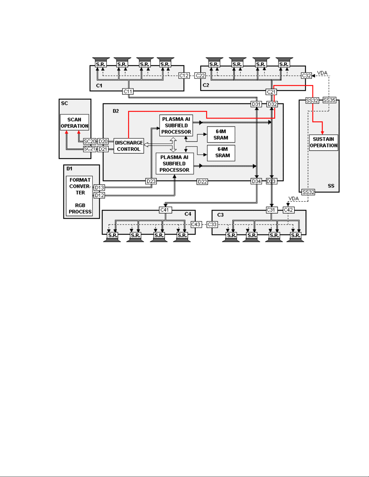
D2 Board
Figure 21
The D2 board provides the scan, sustain and data drive signals. The scan pulses
are output to the SC board. The sustain pulses are output to the SS board. The
data drive signals are output to the C1, C2, C3 and C4 boards. The C1 board
drives the Upper right portion of the panel; the C2 board drives the upper left
portion. The C3 and C4 boards drive the lower right and left portions of the panel
respectively.
23
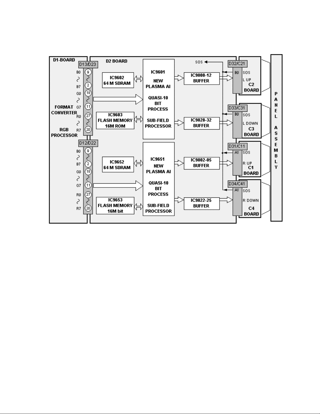
D2 Board details
Figure 22
The Plasma AI (Adaptive brightness Intensifier) circuits analyze the video
program level for the distribution of dark and bright components. The upper and
lower eight bit video signals are memorized into two Plasma AI processors
IC9651 and IC9601. The Plasma AI circuits converts the 8 bit signal data to 10
bit signal data. The Flash memories contain the algorithms for the AI circuit. Two
AI processors are used to speed up the scanning process and control the
number of sustain periods. This increases the brightness and improves the
contrast ratio.
24
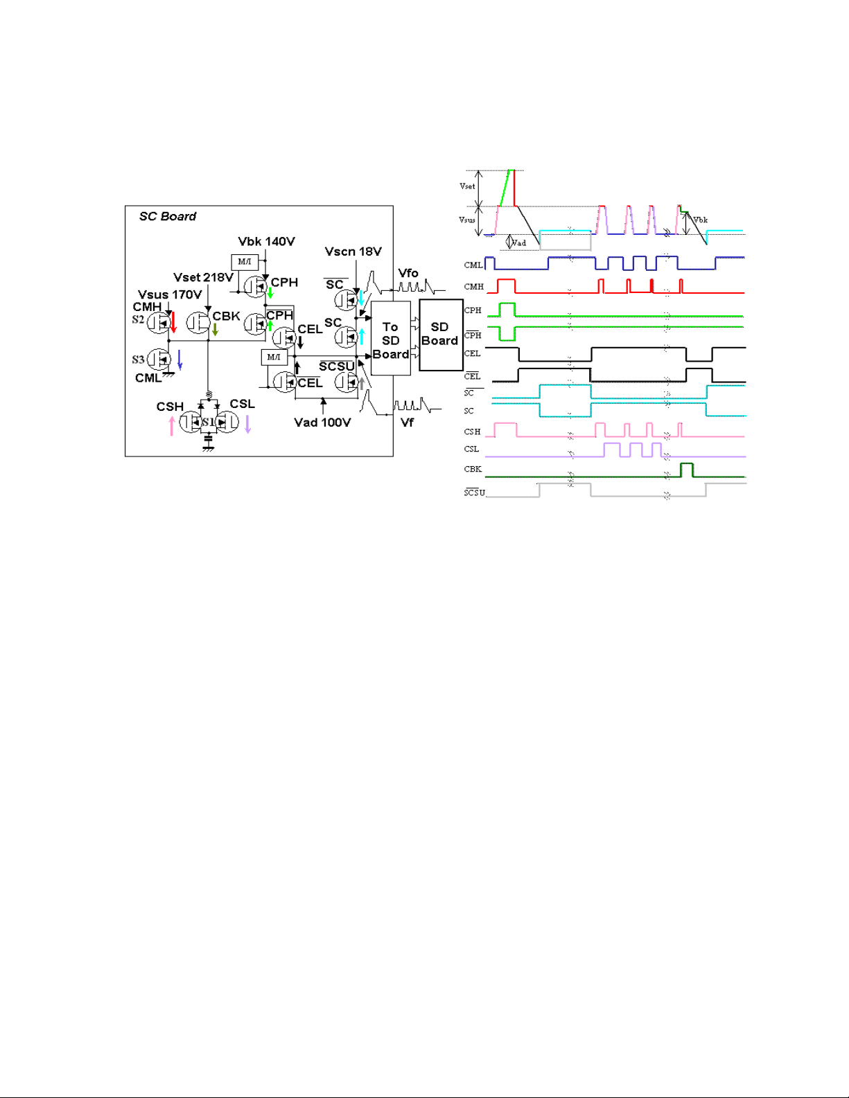
SC Board Explanation
Figure 23
25
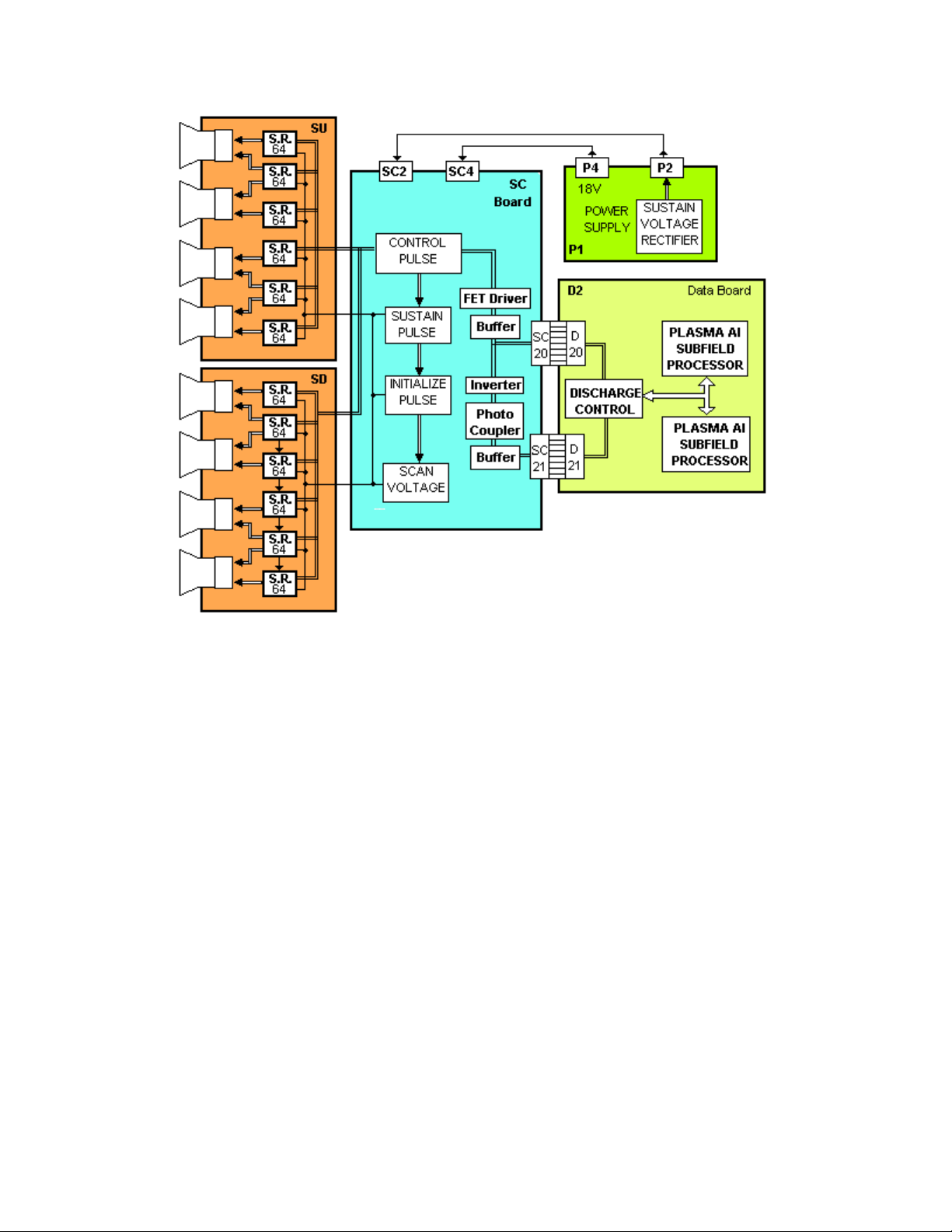
Figure 24
The SC Board consists of buffers and drivers used to generate the scan signals
to the panel. The buffers provide isolation between the D2 board and the drivers.
Connector SC20 provides the drive voltages (140V, 100V and 18V). Connector
SC21 provides trigger signals to switch the FET transistors. The D2 board
switches the FETs on and off to create the distinctive scan signal. Each trigger
signal switches a drive FET creating a portion of the waveform. For example,
applying the CPH signal to the 140V FET creates the peak portion of the
waveform, see figure 23.
26
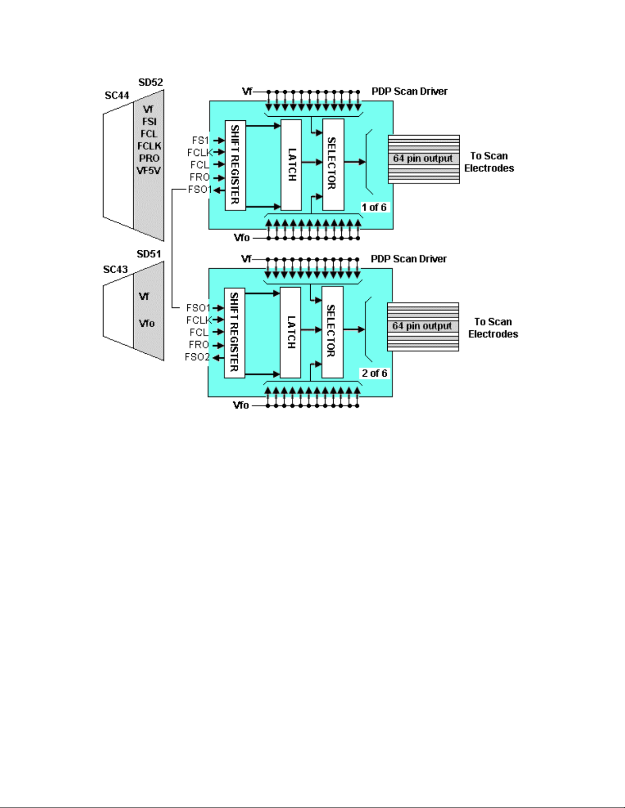
Figure 25
After the scan waveform is developed on the SC Board, it is applied to the SU
and SD boards for de-multiplexing. The signal is input to a series of shift registers
inside the PDP scan driver IC. Figure 25 shows an example of the demultiplexing circuit. There are six driver ICs on the SU board and six on the SD
board.
27
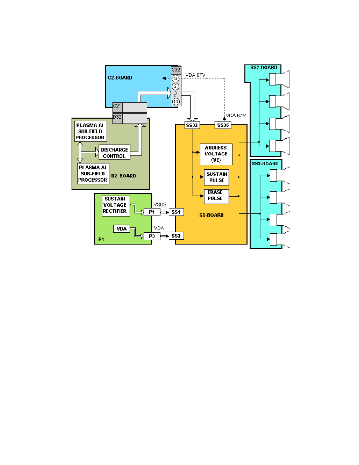
SS Board Explanation
Figure 26
After the video signal is processed on the D2 board, the sustain and erase pulses
are output to the SS board. The erase pulse is output at the beginning of each
scan period. The pulse is applied to the SS2 and SS3 boards to remove the
previous charge for the upper and lower sections of the display panel.
The sustain pulses are also developed on the D2 board and are applied after the
scan periods.
28
 Loading...