

Panasonic TH-103PF10WK, TH-103PF10TK, TH-103PF10RK Service manual
Order Number ITD0711079CE
High Definition Plasma Display
Model No. TH-103PF10WK
Model No. TH-103PF10TK
Model No. TH-103PF10RK
GPF10D Chassis
TABLE OF CONTENTS
1 Safety Precautions----------------------------------------------- 3
1.1. General Guidelines---------------------------------------- 3
2 Warning-------------------------------------------------------------- 4
2.1. Prevention of Electrostatic Discharge (ESD)
to Electrostatically Sensitive (ES) Devices---------- 4
2.2. About lead free solder (PbF)---------------------------- 5
3 Service Navigation----------------------------------------------- 6
3.1. Service Hint------------------------------------------------- 6
3.2. Applicable signals ----------------------------------------- 8
4 Specifications ----------------------------------------------------10
5 Service Mode -----------------------------------------------------11
5.1. CAT (Computer Aided Test) mode-------------------11
5.2. IIC mode structure (following items value is
sample data)-----------------------------------------------15
5.3. Option Setting ---------------------------------------------16
6 Troubleshooting Guide----------------------------------------18
6.1. Self Check--------------------------------------------------18
6.2. No Power---------------------------------------------------20
6.3. No Picture --------------------------------------------------20
6.4. Local screen failure --------------------------------------21
7 Disassembly and Assembly Instructions ---------------22
7.1. Rear Cover and Board----------------------------------22
7.2. Location of Rear Cover screws-----------------------23
7.3. Removal of Side Angle (L), (R) -----------------------26
7.4. Removal of HA-Board-----------------------------------27
PAGE PAGE
7.5. Removal of HDMI-Board ------------------------------28
7.6. Removal of DS-Board --------------------- ------------- 28
7.7. Removal of HX-Board-----------------------------------28
7.8. Removal of DN-Board ---------------------------------- 29
7.9. Removal of PB-Board----------------------------------- 29
7.10. Removal of H5-Board-----------------------------------29
7.1 1. Removal of D-Board ------------------------------------ 30
7.12. Removal of P-Board (MULTI_1), (MULTI_2)------30
7.13. Removal of P-Board (SUS_1), (SUS_2)----------- 31
7.14. Removal of F-Board ------------------------------------ 31
7.15. Removal of PC-Board ------------- --------------------- 31
7.16. Removal of SU-Board ------------- --------------------- 32
7.17. Removal of SM-Board ----------------------------------33
7.18. Removal of SD-Board ------------- --------------------- 33
7.19. Removal of SC-Board ---------------------------------34
7.20. Removal of SC2-Board -------------------------------- 35
7.21. Removal of S1-Board and V2-Board---------------- 35
7.22. Removal of SS2-Board --------------------------------36
7.23. Removal of SS3-Board --------------------------------36
7.24. Removal of SS-Board ----------------------------------37
7.25. Removal of Fan-------------------------------------------38
7.26. Removal of C1-Board-----------------------------------39
7.27. Removal of C2-Board-----------------------------------39
7.28. Removal of C3-Board-----------------------------------40
7.29. Removal of C4-Board-----------------------------------41
© 2007 Matsushita Electric Industrial Co., Ltd. All
rights reserved. Unauthorized copying and distribution is a violation of law.

TH-103PF10WK/TK/RK
7.30. Removal of C5-Board-----------------------------------41
7.31. Removal of C6-Board-----------------------------------42
7.32. Removal of C7-Board-----------------------------------42
7.33. Removal of C8-Board-----------------------------------43
7.34. Removal of C9-Board-----------------------------------43
7.35. Removal of CX-Board-----------------------------------44
7.36. Removal of CY-Board-----------------------------------44
7.37. Removal of CZ-Board-----------------------------------45
7.38. Removal of DR1-Board (A)----------------------------45
7.39. Removal of DR1-Board (B)----------------------------46
7.40. Removal of DR2-Board (A)----------------------------46
7.41. Removal of DR2-Board (B)----------------------------46
7.42. Removal of CD-Board-----------------------------------47
7.43. Removal of AC Inlet -------------------------------------48
7.44. Removal of Cabinet and Front Glass--------------48
7.45. Removal of V1-Board and V3-Board ---------------- 51
7.46. Removal of Plasma Panel -----------------------------51
8 Measurements and Adjustments --------------------------58
8.1. Adjustment Procedure ----------------------------------58
8.2. Adjustment-------------------------------------------------62
9 Block Diagram ---------------------------------------------------67
9.1. DiagramNote ----------------------------------------------67
9.2. Main (1 of 2) Block Diagram---------------------------68
9.3. Main (2 of 2) Block Diagram---------------------------69
9.4. P-Board (1 of 2) and F-Board Block Diagram-----70
9.5. P-Board (2 of 2) Block Diagram ----------------------71
9.6. HA, HX, PC, PB, V1, V2 and V3-Board Block
Diagram-----------------------------------------------------72
9.7. HDMI-Board (1 of 2) Block Diagram ----------------73
9.8. HDMI-Board (2 of 2) Block Diagram ----------------74
9.9. DS-Board (1 of 2) and H3-Board Block
Diagram-----------------------------------------------------75
9.10. DS-Board (2 of 2) Block Diagram--------------------76
9.11. DN-Board (1 of 2) Block Diagram--------------------77
9.12. DN-Board (2 of 2) Block Diagram--------------------78
9.13. D-Board (1 of 2) Block Diagram----------------------79
9.14. D-Board (2 of 2) Block Diagram----------------------80
9.15. C1, C2, CY and CZ-Board Block Diagram---------81
9.16. C2, C3, CX and CY-Board Block Diagram---------82
9.17. C4, C5, C8 and C9-Board Block Diagram---------83
9.18. C5, C6, C7 and C8-Board Block Diagram---------84
9.19. SC2 and S1-Board Block Diagram ------------------85
9.20. SC-Board Block Diagram ------------------------------86
9.21. SU, SM and SD-Board Block Diagram -------------87
9.22. SS, SS2 and SS3-Board Block Diagram ----------- 88
9.23. DR1, DR2 and CD-Board Block Diagram----------89
10 Wiring Connection Diagram---------------------------------90
10.1. Interconnection (1 of 8) Diagram---------------------90
10.2. Interconnection (2 of 8) Diagram---------------------91
10.3. Interconnection (3 of 8) Diagram---------------------92
10.4. Interconnection (4 of 8) Diagram---------------------93
10.5. Interconnection (5 of 8) Diagram---------------------94
10.6. Interconnection (6 of 8) Diagram---------------------95
10.7. Interconnection (7 of 8) Diagram---------------------96
10.8. Interconnection (8 of 8) Diagram---------------------97
10.9. Lead Wiring (1) -------------------------------------------98
10.10. Lead Wiring (2) -------------------------------------------99
10.11. Lead Wiring (3) ----------------------------------------- 100
10.12. Lead Wiring (4) ----------------------------------------- 101
10.13. Lead Wiring (5) ----------------------------------------- 102
10.14. Lead Wiring (6) ----------------------------------------- 103
10.15. Lead Wiring (7)------------------------------------------104
10.16. Lead Wiring (8)------------------------------------------105
10.17. Lead Wiring (9)------------------------------------------106
11 Exploded View and Replacement Parts List----------107
2
TH-103PF10WK/TK/RK
1 Safety Precautions
1.1. General Guidelines
1. When conducting repairs and servicing, do not attempt to modify the equipment, its parts or its materials.
2. When wiring units (with cables, flexible cables or lead wires) are supplied as repair parts and only one wire or some of the
wires have been broken or disconnected, do not attempt to repair or re-wire the units. Replace the entire wiring unit instead.
3. When conducting repairs and servicing, do not twist the Faston connectors but plug them straight in or unplug them straight
out.
4. When servicing, observe the original lead dress. If a short circuit is found, replace all parts which have been overheated or
damaged by the short circuit.
5. After servicing, see to it that all the protective devices such as insulation barriers, insulation papers shields are properly
installed.
6. After servicing, make the following leakage current checks to prevent the customer from being exposed to shock hazards.
1.1.1. Leakage Current Cold Check
1. Unplug the AC cord and connect a jumper between the
two prongs on the plug.
2. Measure the resistance value, with an ohmmeter,
between the jumpered AC plug and each exposed metallic cabinet part on the equipment such as screwheads,
connectors, control shafts, etc. When the exposed metallic part has a return path to the chassis, the reading
should be between 1Mohm and 5.2Mohm.
When the exposed metal does not have a return path to
the chassis, the reading must be .
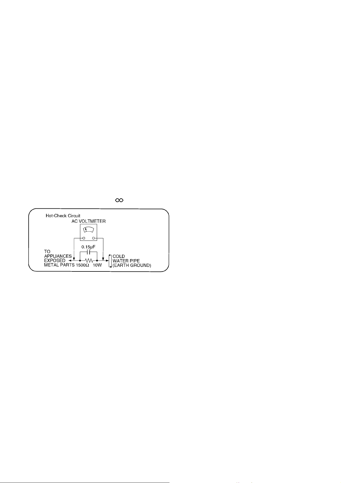
Figure 1
1.1.2. Leakage Current Hot Check (See
Figure 1.)
1. Plug the AC cord directly into the AC outlet. Do not use
an isolation transformer for this check.
2. Connect a 1.5kohm, 10 watts resistor, in parallel with a
0.15µF capacitors, between each exposed metallic part
on the set and a good earth ground such as a water pipe,
as shown in Figure 1.
3. Use an AC voltmeter, with 1000 ohms/volt or more sensitivity, to measure the potential across the resistor.
4. Check each exposed metallic part, and measure the voltage at each point.
5. Reverse the AC plug in the AC outlet and repeat each of
the above measurements.
6. The potential at any point should not exceed 0.75 volts
RMS. A leakage current tester (Simpson Model 229 or
equivalent) may be used to make the hot checks, leakage
current must not exceed 1/2 milliamp. In case a measurement is outside of the limits specified, there is a possibility
of a shock hazard, and the equipment should be repaired
and rechecked before it is returned to the customer.
3
TH-103PF10WK/TK/RK
2Warning
2.1. Prevention of Electrostatic Discharge (ESD) to Electrostatically Sensitive (ES) Devices
Some semiconductor (solid state) devices can be damaged easily by static electricity. Such components commonly are called Electrostatically Sensitive (ES) Devices. Examples of typical ES devices are integrated circuits and some field-effect transistors and
semiconductor "chip" components. The following techniques should be used to help reduce the in cidence of component da mage
caused by electrostatic discharge (ESD).
1. Immediately before handling any semiconductor component or semiconductor-equipped assembly, drain off any ESD on your
body by touching a known earth ground. Alternatively, obt ain and wear a commercially available discharging ESD wrist strap,
which should be removed for potential shock reasons prior to applying power to the unit under test.
2. After removing an electrical assembly equipped with ES devices, p lace the assembl y on a conducti ve surface such as a luminum foil, to prevent electrostatic charge buildup or exposure of the assembly.
3. Use only a grounded-tip soldering iron to solder or unsolder ES devices.
4. Use only an anti-static solder removal device. Some solder removal devices not classified as "anti-static (ESD protected)"
can generate electrical charge sufficient to damage ES devices.
5. Do not use freon-propelled chemicals. These can generate electrical charges sufficient to damage ES devices.
6. Do not remove a replacement ES device from its protective package until immediately before you are ready to install it. (Most
replacement ES devices are packaged with leads electrically shorted together by conductive foam, aluminum foil or comparable conductive material).
7. Immediately before removing the protective material from the leads of a replacement ES device, touch the protective material
to the chassis or circuit assembly into which the device will be installed.
Caution
Be sure no power is applied to the chassis or circuit, and observe all other safety precautions.
8. Minimize bodily motions when handling unpackaged replacement ES devices. (Otherwise ham less motion such as the brushing together of your clothes fabric or the lifting of your foot from a carpeted floor can generate static electricity (ESD) sufficient
to damage an ES device).
4
TH-103PF10WK/TK/RK
2.2. About lead free solder (PbF)
Note: Lead is listed as (Pb) in the periodic table of elements.
In the information below, Pb will refer to Lead solder, and PbF will refer to Lead Free Solder.
The Lead Free Solder used in our manufacturing process and discussed below is (Sn+Ag+Cu).
That is Tin (Sn), Silver (Ag) and Copper (Cu) although other t ypes ar e availa ble .
This model uses Pb Free solder in it’s manufacture due to environmental conservation issues. For service and repair work, we’d
suggest the use of Pb free solder as well, although Pb solder may be used.
PCBs manufactured using lead free solder will have the PbF within a leaf Symbol PbF stamped on the back of PCB.
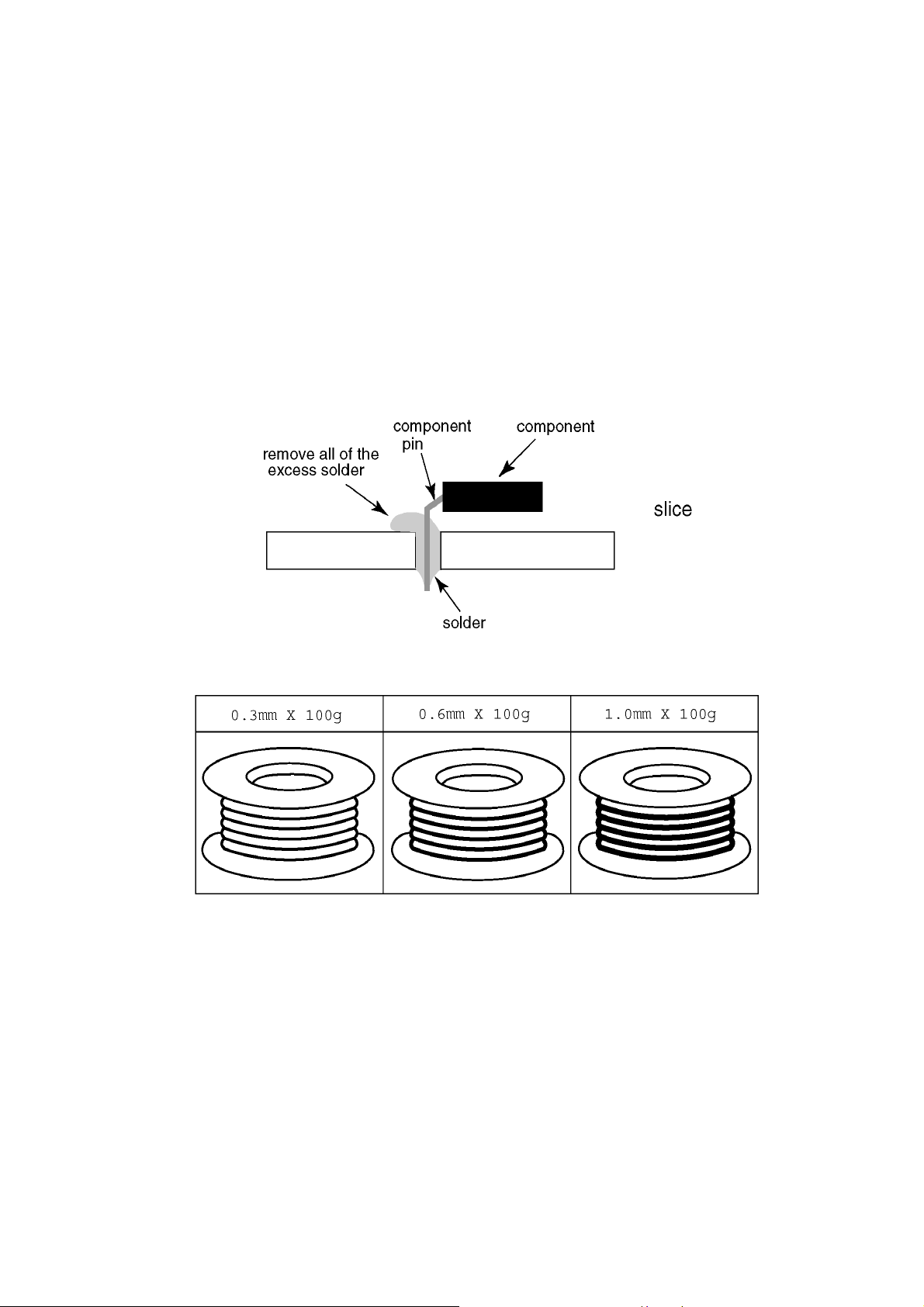
Caution
• Pb free solder has a higher melting point than st andard solder . Typically the melting point is 50 ~ 70 °F (30~40 °C) higher. Please
use a high temperature soldering iron and set it to 700 ± 20 °F (370 ± 10 °C).
• Pb free solder will tend to splash when heated too high (about 1100 °F or 600 °C).
If you must use Pb solder, please completely remove all of the Pb free solder on the pins or solder area before applying Pb sol der. If this is not practical, be sure to heat the Pb free solder until it melts, before applying Pb solder.
• After applying PbF solder to double layered boards, please check the component side for excess solder which may flow onto the
opposite side. (see figure below)
Suggested Pb free solder
There are several kinds of Pb free solder available for purchase. This product uses Sn+Ag+Cu (tin, silver, copper) solder. However, Sn+Cu (tin, copper), Sn+Zn+Bi (tin, zinc, bismuth) solder can also be used.
5
TH-103PF10WK/TK/RK
3 Service Navigation
3.1. Service Hint
6
TH-103PF10WK/TK/RK
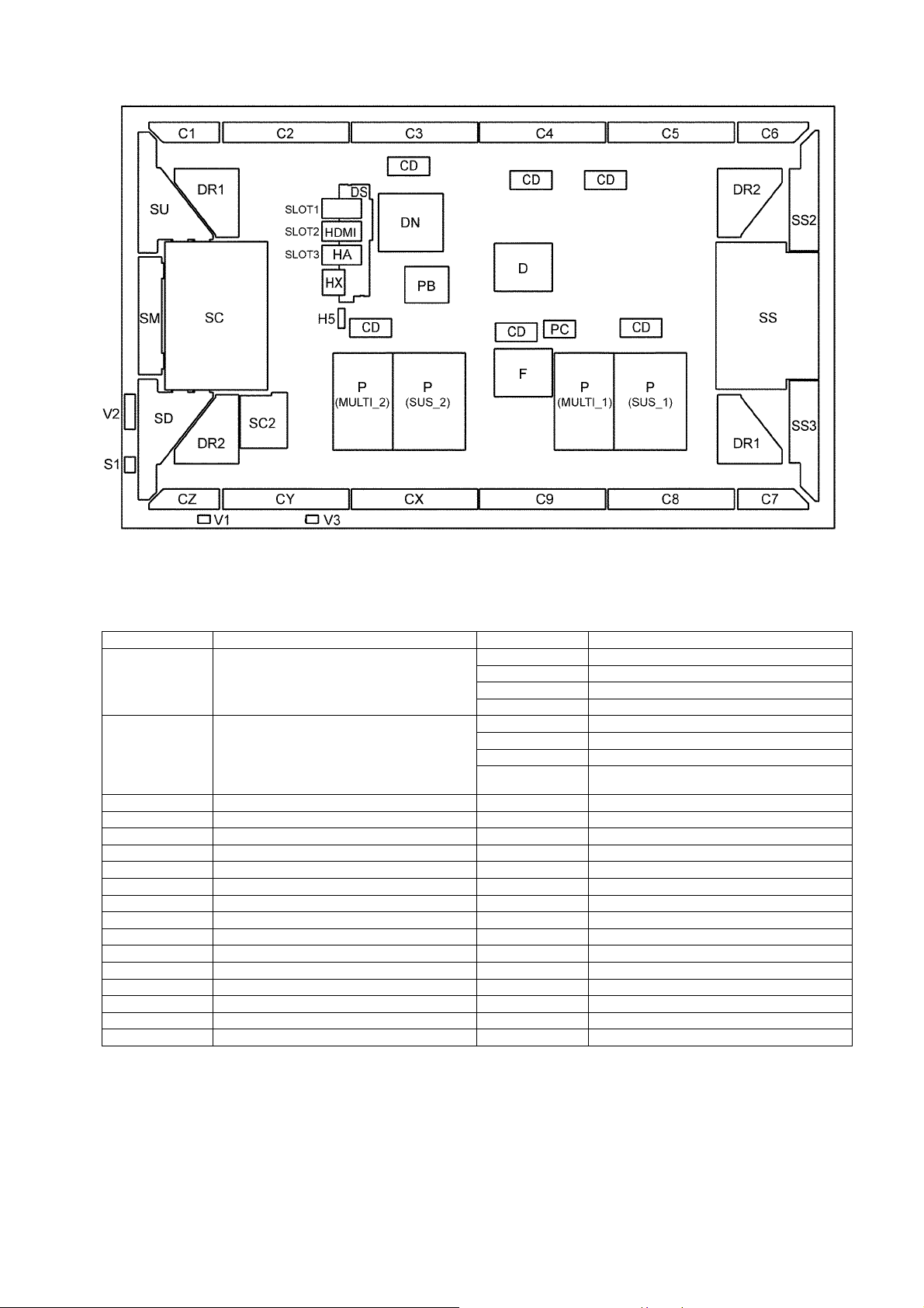
Board Name Function Board Name Function
D Digital Signal Processor,
Format Converter,
Plasma AI Processor
Sub-Field Processor
DS Slot Interface (Audio / Video / Sync Input
Switch),
SYNC Processor, Audio Processor,
Speaker Out Amplifier,
DC-DC Converter
SS Sustain Drive V2 Key Scan
SC Scan Drive V3 Remocon Receiver
SC2 DC-DC Converter For Scan Drive PB Fan Control
SU Scan Out (Upper) P(SUS_1/2) Power Supply
SM Scan Out (Middle) P(MULTI_1/2) Power Supply
SD Scan Out (Lower) F Line Filter
C1 Data Drive (1) PC Power Control
C2 Data Drive (2) HX PC / RS-232C
C3 Data Drive (3) HA BNC Component Video
C4 Data Drive (4) DN Digital Signal Processor, Microcomputer
C5 Data Drive (5) HDMI Dual HDMI
C6 Data Drive (6) CD C-Board / D-Board Connection
C7 Data Drive (7) DR1 Energy Data Recovery
C8 Data Drive (8) DR2 Energy Data Recovery
C9 Data Drive (9)
CX Data Drive (X)
CY Data Drive (Y)
CZ Data Drive (Z)
H5 Audio Out
S1 Power Switch
SS2 Sustain Out (Upper)
SS3 Sustain Out (Lower)
V1 LED_G, R
Note:
Extension cable kit for Slot Board is supplied as service fixtures and tools.
(Part No. TZSC07040)
7
TH-103PF10WK/TK/RK
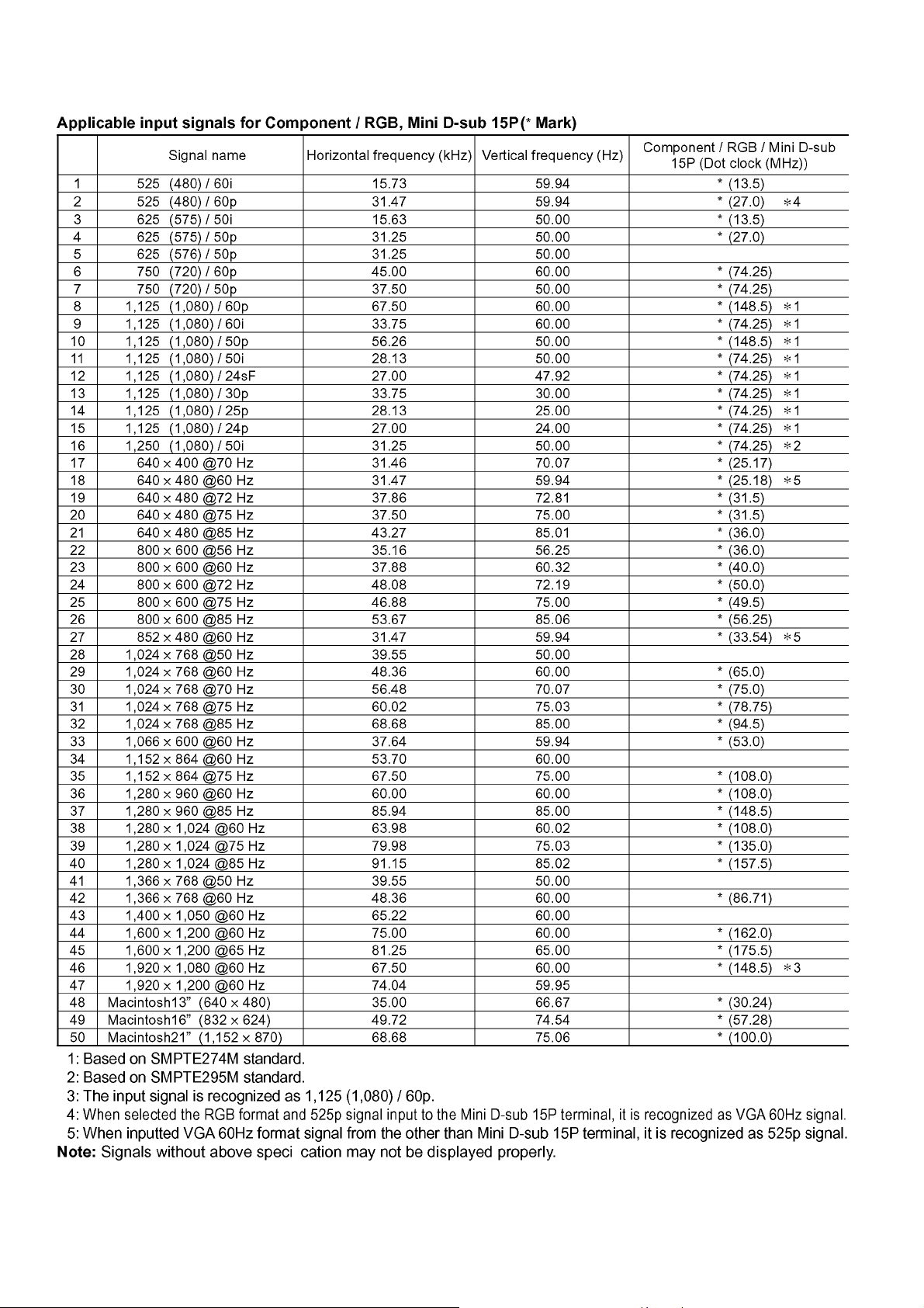
3.2. Applicable signals
8
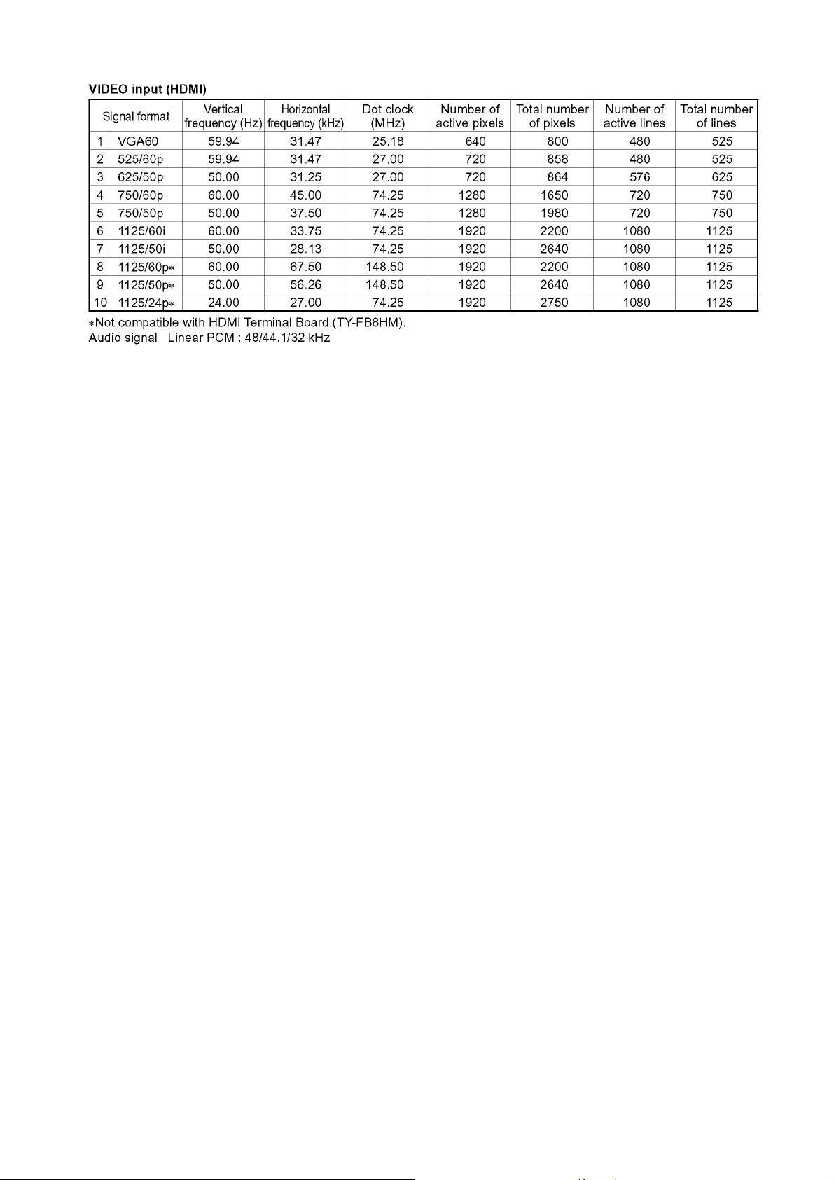
TH-103PF10WK/TK/RK
9

TH-103PF10WK/TK/RK
4 Specifications
Power Source (WK/RK) 220 V - 240V AC, 50 / 60Hz
Power Source (TK) 220 V - 240 V AC, 50 / 60Hz (single phase)
Power Consumption
Power on 1,500 W
Stand-by condition Save OFF 1.0 W, Save ON 0.9 W
Power off condition 0.5 W
Plasma Display panel Drive method: AC type 103-inch, 16:9 aspect ratio
Screen size 2,269 mm (W) × 1,277 mm (H) × 2,604 mm (diagonal)
(No. of pixels) 2,073,600 (1,920 (W) × 1,080 (H)) [5,760 × 1,080 dots]
Operating condition
Temperature 0 °C - 40 °C
Humidity 20 % - 80 %
Applicable signals
Scanning format
PC signals VGA, SVGA, XGA, SXGA,
Connection terminals
HDMI A-B TYPE A Connector x 2
COMPONENT / RGB IN Y / G (BNC) with sync 1.0 Vp-p (75-ohm)
PC IN (HIGH-DENSITY Mini D-SUB 15PIN) Y or G with sync 1.0 Vp-p (75-ohm)
SERIAL EXTERNAL CONTROL TERMINAL (D-SUB 9PIN) RS-232C COMPATIBLE
AUDIO OUT RCA PIN JACK × 2 (L / R)
Accessories Supplied
Remote Control Transmitter EUR7636070R
Batteries R6 Size x 2
Fixing bands TMME203 × 2
Dimensions (W × H × D) 2,414 mm × 1,421 mm × 129 mm (141 mm when including protruding portion of slots)
Mass (weight) approx. 220.0 kg net
525 (480) / 60i 60p, 625 (575) / 50i 50p, 750 (720) / 60p 50p, 1125 (1080) /
60i 60p 50i 50p 24p 25p 30p 24sF,1250 (1080) / 50i
UXGA ..... (compressed)
Horizontal scanning frequency 15 - 110 kHz
Vertical scanning frequency 48 - 120 Hz
P
/ B (BNC), PR / R (BNC) 0.7 Vp-p (75-ohm)
B
AUDIO IN (RCA PIN JACK × 2) 0.5 Vrms (high impedance)
Y or G without sync 0.7 Vp-p (75-ohm)
B / P
/ CB: 0.7 Vp-p (75-ohm)
B
R / P
/ CR: 0.7 Vp-p (75-ohm)
R
HD / VD: 1.0 - 5.0 Vp-p (high impedance)
AUDIO IN (M3 JACK) 0.5 Vrms (high impedance)
OUTPUT LEVEL : VARIABLE (- - 0 dB)
[INPUT 1 kHz / 0 dB, 10 k-ohm Load]
Notes:
• Design and specifications are subject to change without notice. Mass and dimensions shown are approximate.
• This equipment complies with standards. AS/NZS60065, CISPRE22 Class-B (TH-103PF10WK)
10

5 Service Mode
5.1. CAT (Computer Aided Test) mode
TH-103PF10WK/TK/RK
To exit the CAT mode, access the ID mode and switch off the main power.
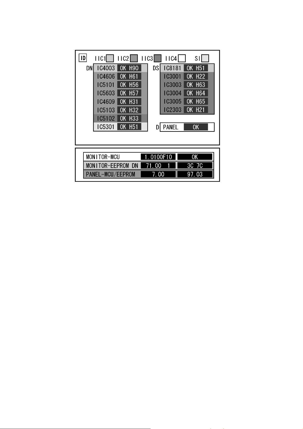
5.1.1. IIC mode
Select the IIC mode by Up / Down button on the remote control at the front page of CAT mode and then press the Action button
on the remote control.
Subject and item are mentioned on “IIC mode structure”.
To exit the IIC mode, press the R button on the remote control.
11
TH-103PF10WK/TK/RK
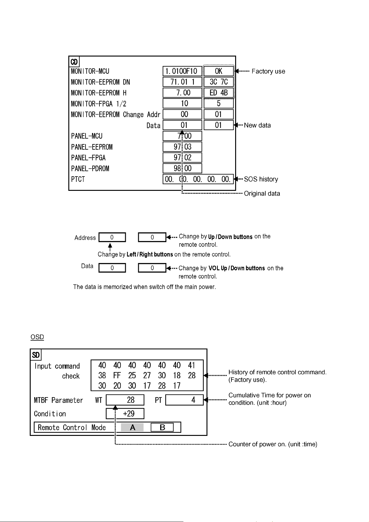
5.1.2. CD mode
Select the CD mode by Up / Down button on the remote control at the front page of CAT mode and then press the Mute button on
the remote control more than 3 seconds.
Microcomputer software version (IC4002), this version can be upgrade by
1. replace of new version IC
2. Loading the new version software from loader tool, TZSC07036.
Memory data change
To exit the CD mode, press the R button on the remote control.
5.1.3. SD mode
Select the SD mode by Up / Down button on the remote control at the front page of CAT mode and then press the Action button
on the remote control.
To exit the SD mode, press the R button on the remote control.
12
TH-103PF10WK/TK/RK
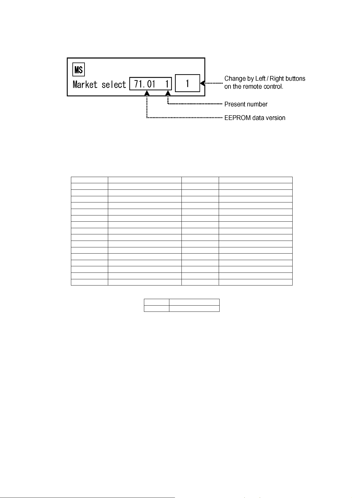
5.1.4. MS mode
Select the MS mode by Up / Down button on the remote control at the front page of CAT mode and then press the Mute button on
the remote control more than 3 seconds.
To exit the MS mode, press the R button on the remote control.
Caution:
Market Select should be set after exchange of DN-Board.
Destination number
Number Destination Number Destination
0 Japan 16 -1 North America 17 -2 Europe 18 China
3 Others 19 China (Hotel)
4 Britain 20 Russia
5 Taiwan 21 Russia (Hotel)
6 Thailand 22 Hong Kong
7--23-8 Japan (Hotel) 24 --
9 North America (Hotel) 25 -10 Europe (Hotel) 26 -11 -- 27 -12 Britain (Hotel) 28 Middle East/Hong Kong
13 -- 29 Middle East/Hong Kong (Hotel)
14 Thailand (Hotel) 30 Australia
15 -- 31 Australia (Hotel)
Default setting
Number Destination
1 North America
13
TH-103PF10WK/TK/RK
5.1.5. ID mode
Select the ID mode by Up / Down button on the remote control at the front page of CAT mode and then press the Mute button on
the remote control more than 3 seconds.
To exit the ID mode, press the R button on the remote control.
14
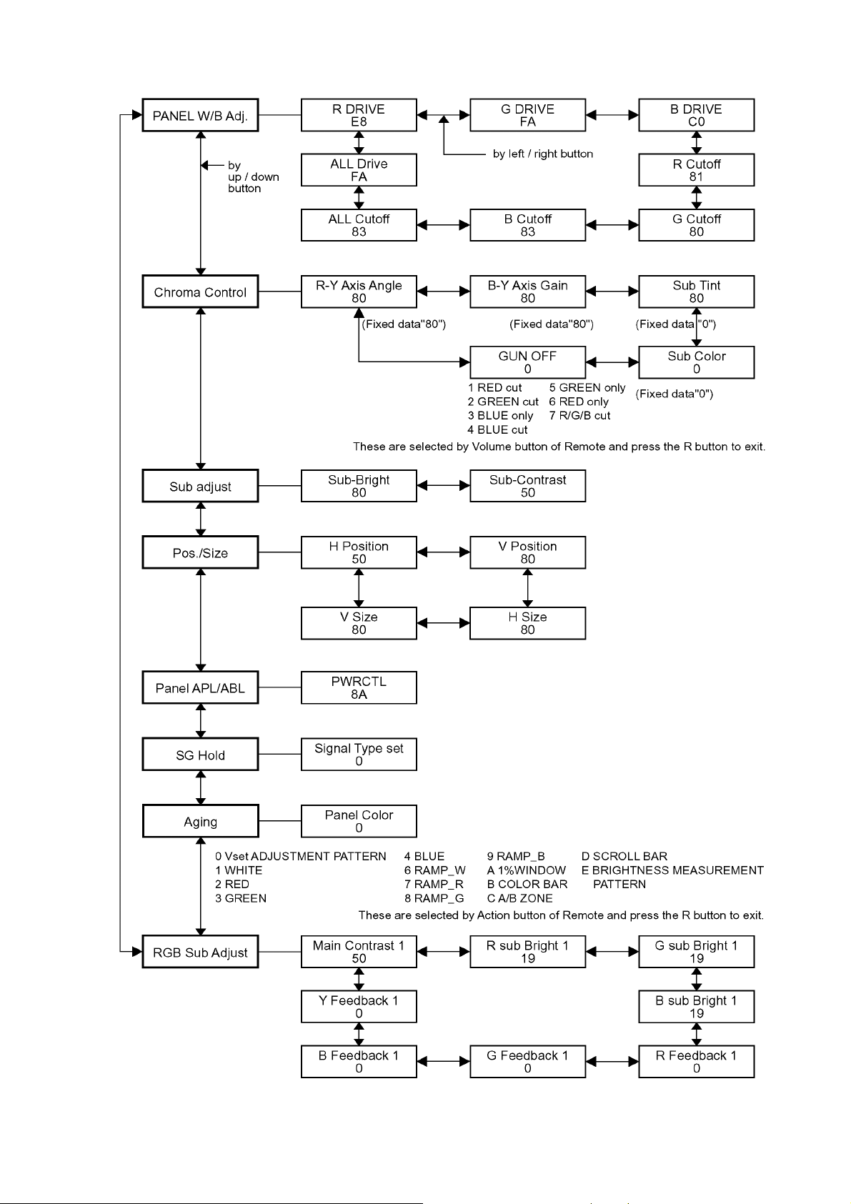
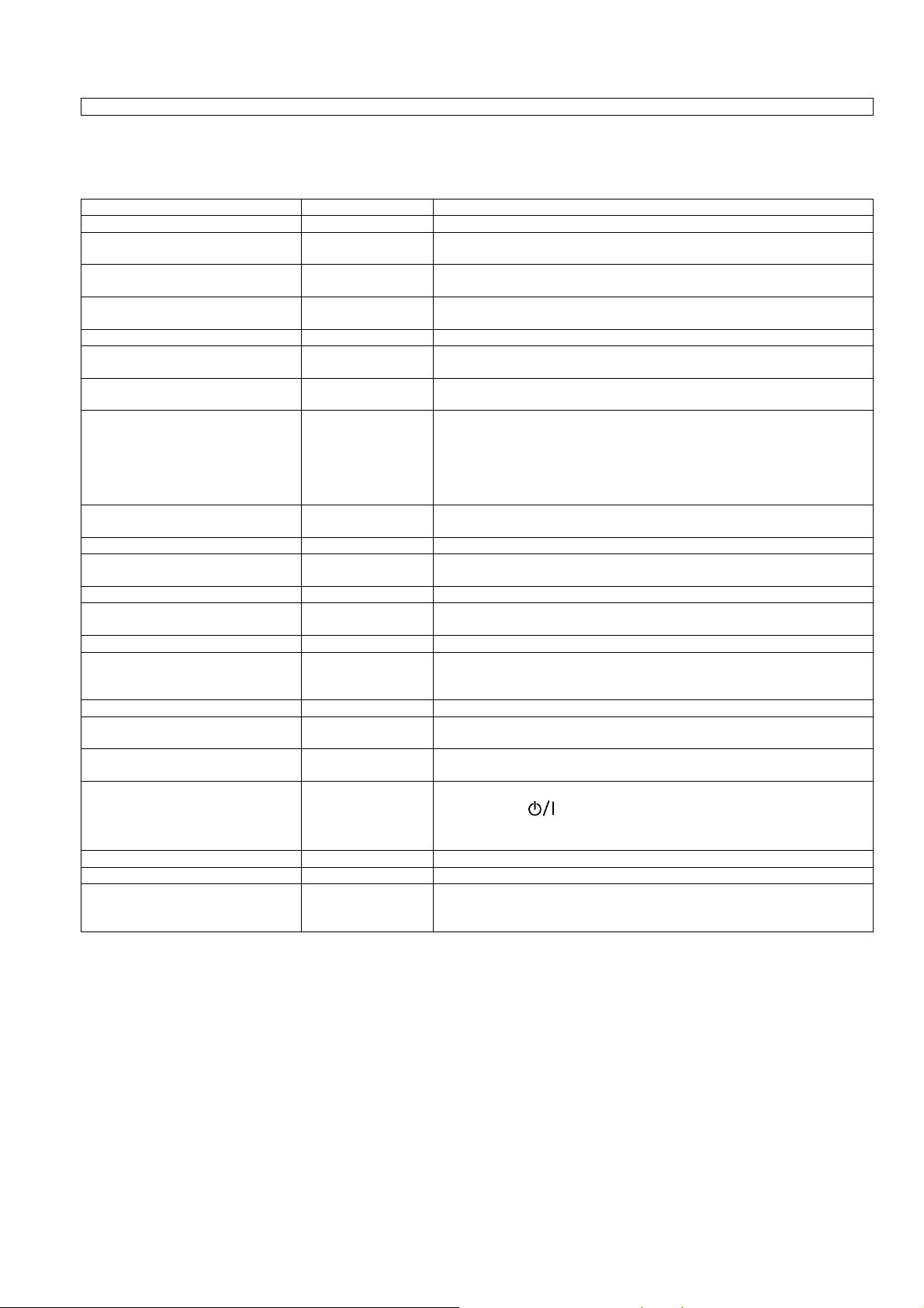
5.2. IIC mode structure (following items value is sample data)
TH-103PF10WK/TK/RK
15
TH-103PF10WK/TK/RK
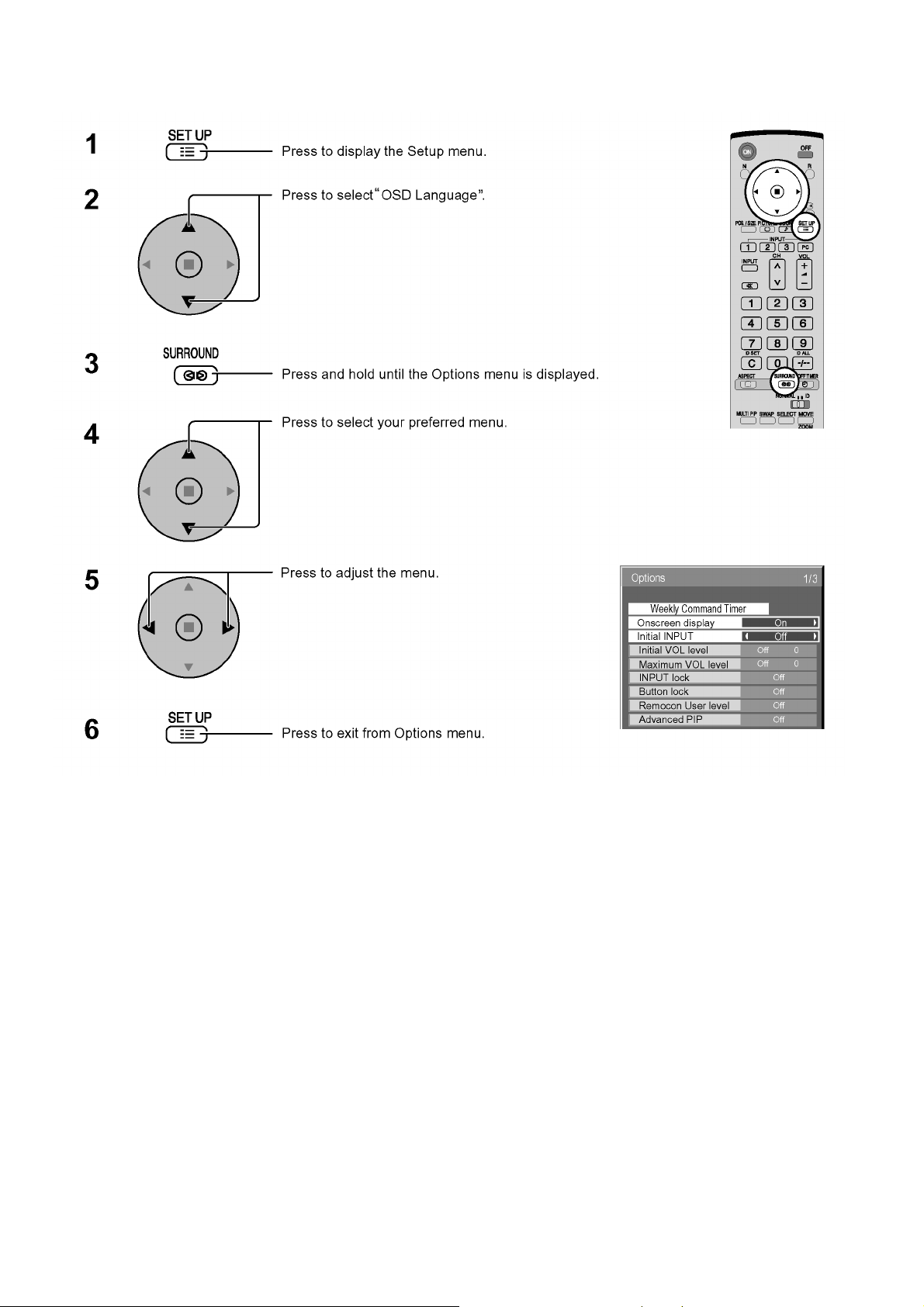
5.3. Option Setting
16
TH-103PF10WK/TK/RK
Option Menu for GPF10D series
GPH10D chassis series have special function and oper ation setting facility called Option Menu. This Option Menu is useful for special function required customers. This should be set at the installation stage.
Option menus default setting Contents
Weekly Command Timer --- Off-timer Sets Weekly Command Timer. Enable/Disable.
Onscreen display On Enable/Disable to display input mode indication after power on and no signal
indication.
Initial INPUT Off Sets the initial input mode when the power is turned on. Allow input mode selec-
Initial VOL level Off Sets the initial volume level when the power is turned on. Allow Volume control
Maximum VOL Level Off Sets the maximum volume to desired level. Volume cannot exceed this level.
INPUT lock Off Fixes the input mode to AV, Component/RGB or PC. Can not change input
Button lock Off Enable/Disable bottom operation buttons (Input, Menu, Enter and/or volume up/
Remocon User Level Off Remote key invalidation.
Advanced PIP Off Off: Sets normal two screen display mode.
Off-timer function Enable Off-timer operation Enable/Disable.
Initial Power Mode Normal Sets the power mode of the unit for when the power recovers from failure or
ID select 0 Set ID number from 0 to 100.
Remote ID Off Remote ID function On/Off.
Serial ID Off Serial ID function On/Off
Display size Off Adjusts the image display size on screen.
Studio W/B Off Set warm mode color temperature to 3,200 Kelvin.
Studio Gain Off Sharpens the contrast for a better view when a part of the image is too light to
Slot power Off Sets the slot power mode while the power is turned on.
Power On Screen Delay Off You can set the power-on delay time of the displays to reduce the power load,
V. Installation Off V. Installation function On/Off (Not used)
Rotate Off The image rotates 180 degrees (up-down)
Serial Slot Select Slot1 Selects the slot which communicates serial.
tion while power is on.
while power is on.
mode by input selection key
down)
Off: Valid key is all key of remote.
User1: Valid key are only Stand-by (ON/OFF), Input, Direct input, Status, Surround, Sound mute On/Off, and volume adjustment.
User2: Valid key is only Stand-by (ON/OFF).
User3: All keys are null and void
On: Sets Advanced PIP mode.
after plugging off and in again.
(While the Remote ID on, standard remote function can not control the unit.)
On: Sets the image display size approximately 95% of the normal image display.
see
Allow Optional Terminal Board insert Slots while power is on.
when you press to turn on the multiple displays that are set together, for
example, on MULTI DISPLAY system.
Set each display’fs setting individually.
Note: The setting of an external command can be set only from the fixed serial
terminal.
Note:
When both main unit buttons and remote control are disabled due to the "Button lock", "Remocon User level" or "Remote ID"
adjustments, set all the values "Off" so that all the buttons are enabled again.
Press the "Volume down" button on main unit together with "R" button on the remote control and hold for more than 5 seconds.
The "SHIPPING" menu is displayed and the lock is released when it disappears.
17
TH-103PF10WK/TK/RK
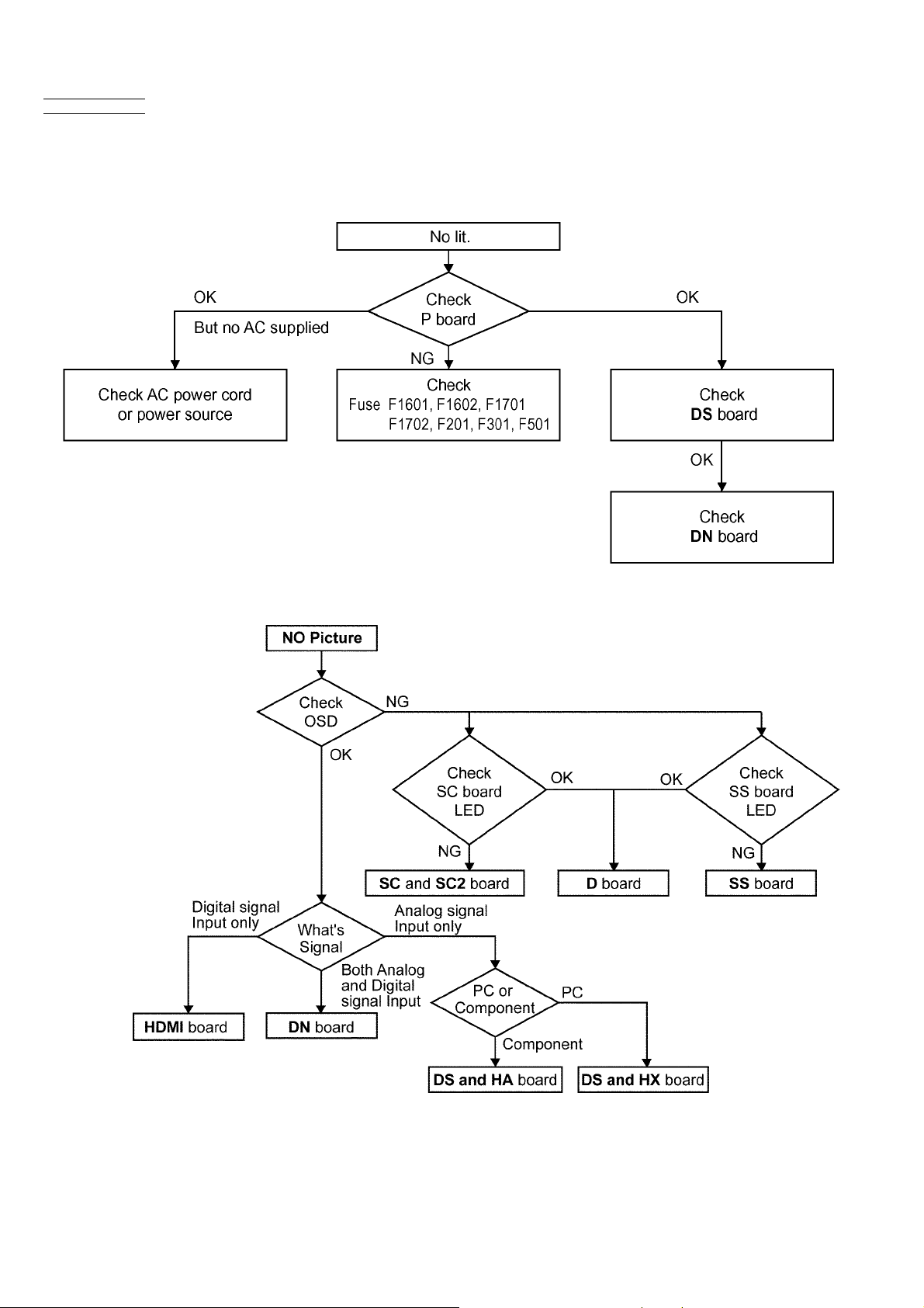
6 Troubleshooting Guide
6.1. Self Check
6.1.1. Display Indication
1. Self-check is used to automatically check the bus line controlled circuit of the Plasma display.
2. To get into the Self-check mode, press the volume down button on the customer controls at the side of the set, at the same
time pressing the OFF-TIMER button on the remote control, and the screen will show.
If the IIC ports have been checked and found to be incorrect.
Or not located then " - - " will appear in place of " OK ".
“ 01 “ in the line of the “ PTCT ” means the number of blinks of the Power LED is 1. (Refer to 7.1.2)
“ H09 “ in the line of the “ PTCT ” is the error code.
To exit Self Check mode, switch off the main power.
Note:
The line of the “ PTCT ” displays when you get into the Self-check mode for the first time only after the Power LED blinks.
18
TH-103PF10WK/TK/RK
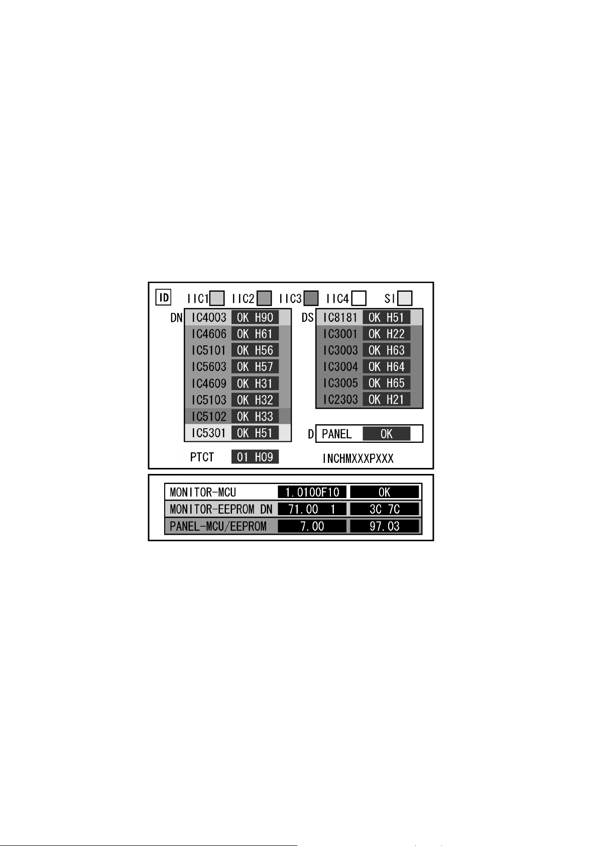
6.1.2. Power LED Blinking timing chart
1. Subject
Information of LED Blinking timing chart.
2. Contents
When an abnormality has occurred to the unit, the protection circuit operates and resets to the stand by mode. At this time,
the defective block can be identified by the number of blinks of the Power LED on the front panel of the unit.
3. Remarks
Above Fan function is operated during the fans are installed.
About blinking LED
19
TH-103PF10WK/TK/RK
6.2. No Power
First check point
There are following 3 states of No Power indication by power LED.
1. No lit.
2. Green is lit then turns red blinking a few seconds later.
3. Only red is lit.
6.3. No Picture
20
TH-103PF10WK/TK/RK
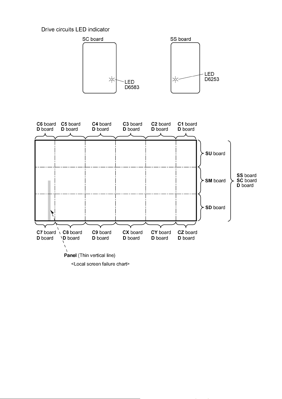
6.4. Local screen failure
Plasma display may have local area failure on the screen. Fig - 1 is the possible defect P.C.B. for each local area.
Fig - 1
21
TH-103PF10WK/TK/RK
7 Disassembly and Assembly Instructions
• To disassemble P.C.B., wait for 1 minute after power was off for discharge from electrolysis capacitors.
• and marks indicate screw positions.
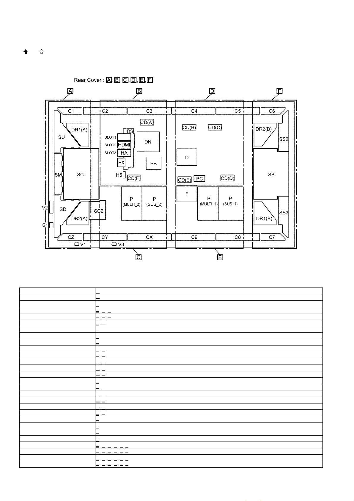
7.1. Rear Cover and Board
Rear Cover required to remove for each board exchange.
Board Name Rear Cover
D-Board D
DS-Board B
SS-Board F
SC-Board A, B, C
SC2-Board A, C
SU-Board A
SM-Board A
SD-Board A
C1-Board A
C2-Board A, B
C3-Board B, D
C4-Board B, D
C5-Board D, F
C6-Board F
C7-Board F
C8-Board E, F
C9-Board C, E
CX-Board C, E
CY-Board A, C
CZ-Board A
H5-Board B
S1-Board A
SS2-Board F
SS3-Board F
V1-Board A, B, C, D, E, F
V2-Board A
V3-Board A, B, C, D, E, F
22
Board Name Rear Cover
PB-Board B
P-Board (MULTI_1) E
P-Board (SUS_1) E
P-Board (MULTI_2) C
P-Board (SUS_2) C
F-Board E
PC-Board D
HX-Board B
HA-Board B
DN-Board B
HDMI-Board B
CD-Board (A) B
CD-Board (B) D
CD-Board (C) D
CD-Board (D) D
CD-Board (E) D
CD-Board (F) B
DR1-Board (A) A
DR1-Board (B) F
DR2-Board (A) A
DR2-Board (B) F
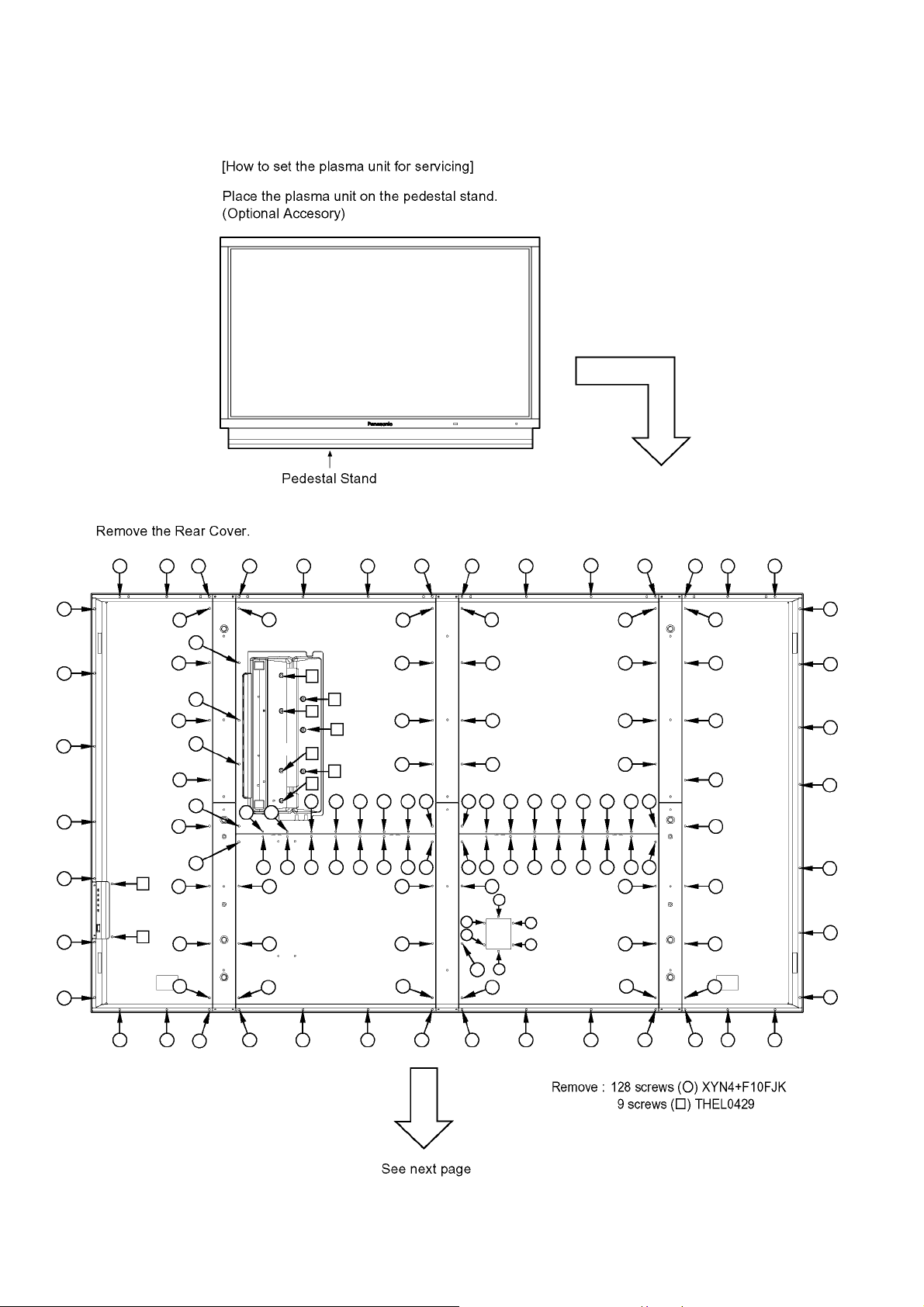
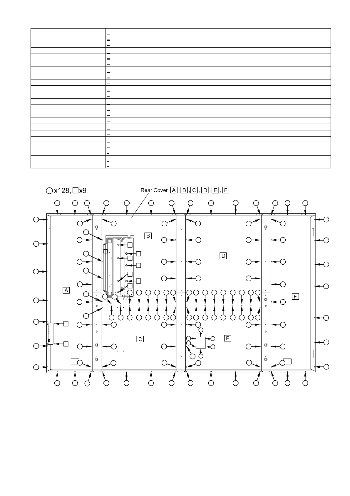
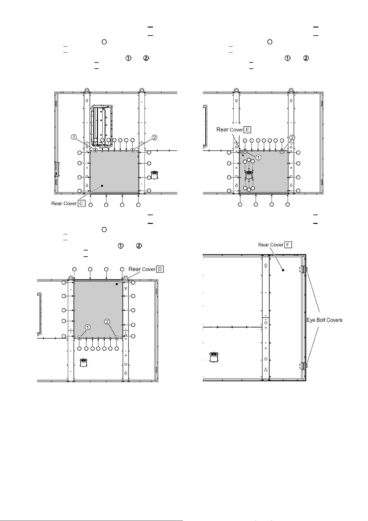
7.2. Location of Rear Cover screws
TH-103PF10WK/TK/RK
23

TH-103PF10WK/TK/RK
7.2.1. Removal of Rear Cover ( A )
1. Remove Eye Bolt Covers.
2. Remove screws (×21 , ×2 ) and then remove the
Rear Cover ( A
).
7.2.2. Removal of Rear Cover ( B )
1. Remove screws (×21 , ×7 ) and then remove the
Rear Cover ( B
Tighten screw first in order of , and when mount-
ing the Rear cover B
).
.
24
TH-103PF10WK/TK/RK
7.2.3. Removal of Rear Cover ( C )
1. Remove screws (× 19 ) and then remove the Rear
Cover ( C
Tighten the screw first in order of and when mount-
ing the Rear Cover C
).
.
7.2.5. Removal of Rear Cover ( E )
1. Remove screws (×25 ) and then remove the Rear
Cover ( E
Tighten screw first in order of and when mounting
the Rear cover E
).
.
7.2.4. Removal of Rear Cover ( D )
1. Remove screws (× 21 ) and then remove the Rear
Cover ( D
Tighten screw first in order of and when mounting
the Rear cover D
).
.
7.2.6. Removal of Rear Cover ( F )
1. Remove Eye Bolt Covers.
25
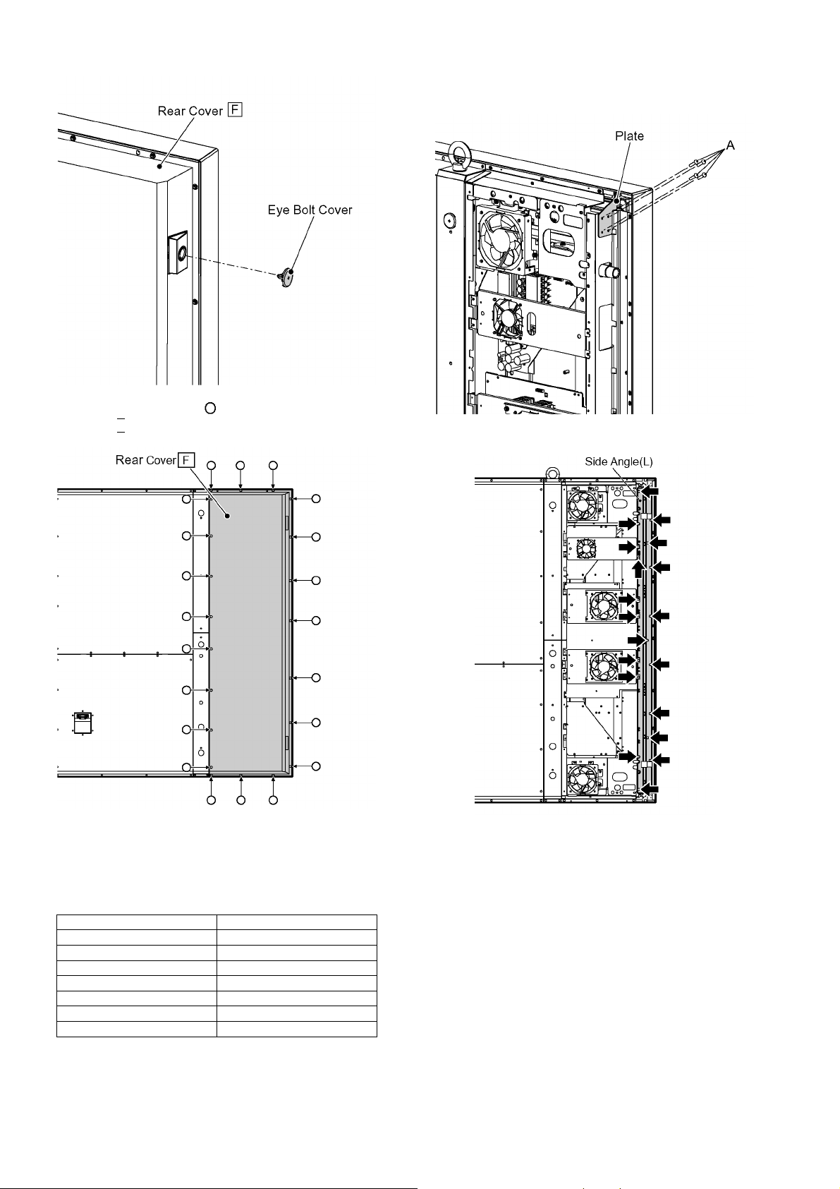
TH-103PF10WK/TK/RK
2. Remove screws (×21 ) and then remove the Rear
Cover ( F
).
7.3.1. Removal of Side Angle (L)
1. Remove 4 screws (A) of the Plate.
2. Remove 19 screws and then remove the Side Angle (L).
7.3. Removal of Side Angle (L), (R)
1. Remove Side Angle (L), (R) beforehand when remove the
following Boards.
Board name Side Angle
SU-Board Side Angle (R)
SM-Board Side Angle (R)
SD-Board Side Angle (R)
SC-Board Side Angle (R)
SS2-Board Side Angle (L)
SS3-Board Side Angle (L)
SS-Board Side Angle (L)
26
TH-103PF10WK/TK/RK
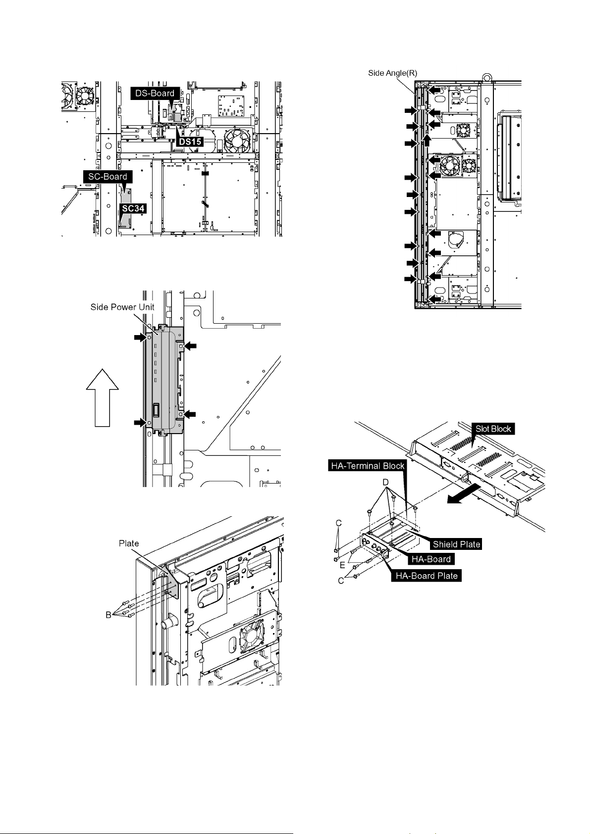
7.3.2. Removal of Side Angle (R)
1. Disconnect the connectors (DS15, SC34).
2. Remove 4 screws, and then side the Side Power Unit
upward.
3. Remode the side Power Unit.
5. Remove 19 screws and then remove the Side Angle (R).
4. Remove 4 screws (B) of the Plate.
7.4. Removal of HA-Board
1. Remove 4 screws (C) and then remove the HA Terminal
Block.
2. Remove 4 screws (D) and remove Shield Plate.
3. Remove 2 Hexagonal-Head screws (E) and then remove
HA-Board.
27
TH-103PF10WK/TK/RK
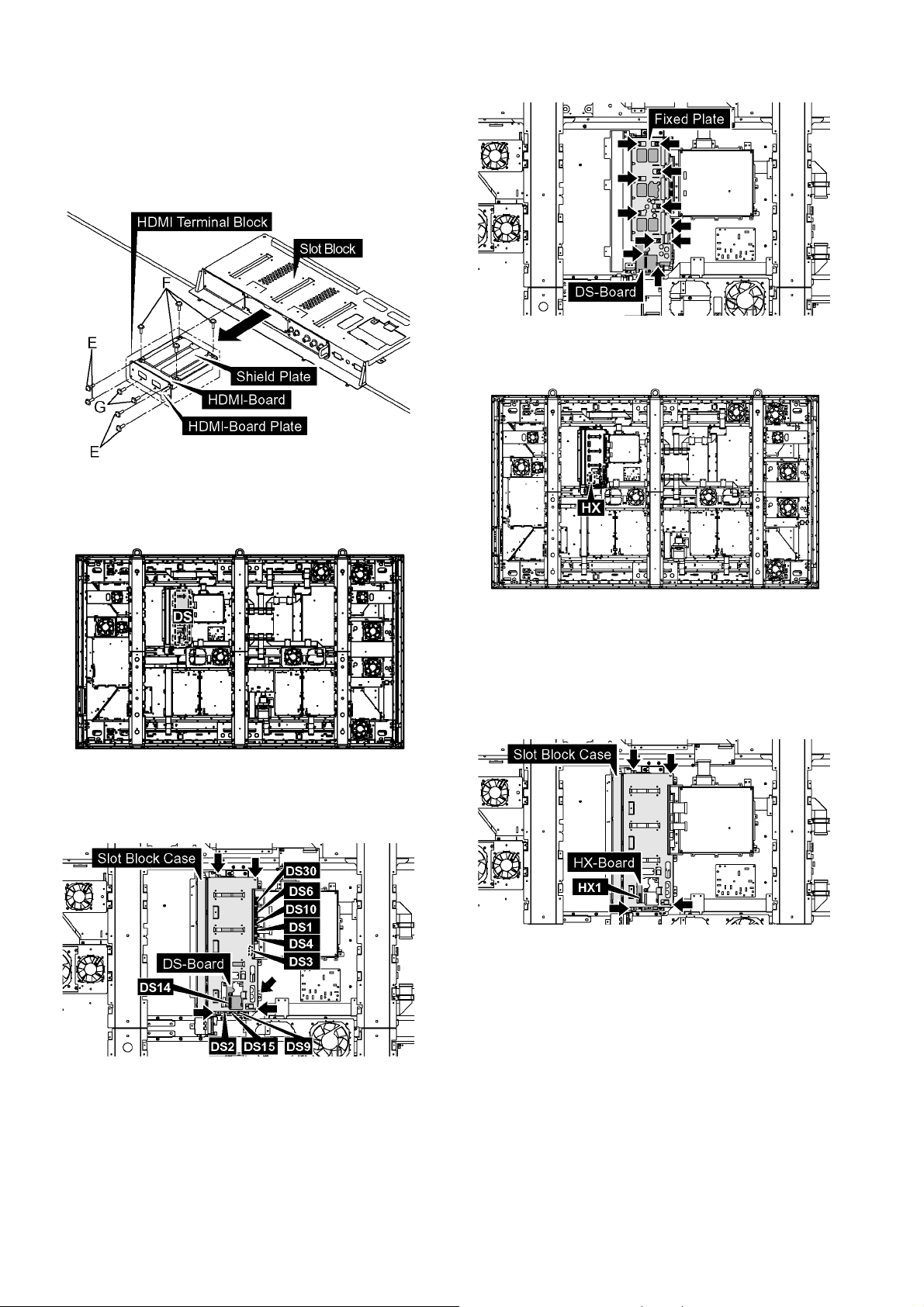
7.5. Removal of HDMI-Board
1. Remove 4 screws (E) and then remove the HDMI Termi nal Block.
2. Remove 4 screws (F) and remove Shield Plate.
3. Remove 2 Hexagonal-Head screws (G) and then remove
HDMI-Board.
7.6. Removal of DS-Board
3. Remove 11 screws and then remove DS-Board.
7.7. Removal of HX-Board
1. Disconnect the connectors (DS1, DS2, DS3, DS4, DS6,
DS9, DS10, DS14, DS15, DS30).
2. Remove 5 screws and then remove the Slot Block Case.
1. Remove the HA Terminal Block.
(Refer to Removal of HA-Board)
2. Remove the HDMI Terminal Block.
(Refer to Removal of HDMI-Board)
3. Disconnect the connectors (HX1).
4. Remove 4 screws and then remove the Slot Block Case.
5. Remove 4 Hexagonal-Head screws (H) and 2 screws on
28
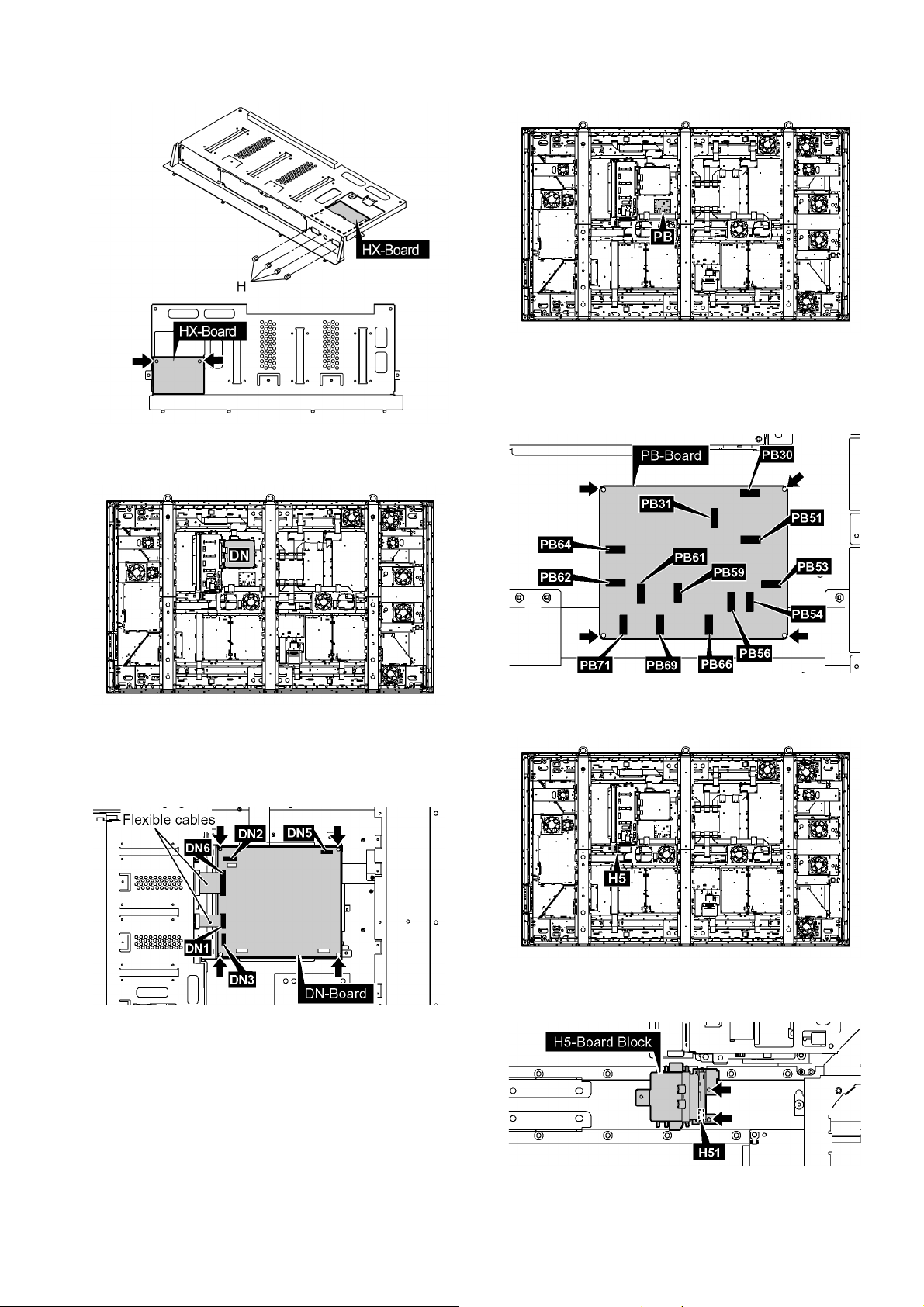
TH-103PF10WK/TK/RK
HX-Board, and then remove HX-Board.
7.8. Removal of DN-Board
7.9. Removal of PB-Board
1. Disconnect the connectors (PB30, PB31, PB51, PB53,
PB54, PB56, PB59, PB61, PB62, PB64, PB66, PB69,
PB71).
2. Remove 4 screws and then remove PB-Board.
1. Remove the flexible cables from the connectors (DN1,
DN6).
2. Disconnect the connectors (DN2, DN3, DN5).
3. Remove 4 screws and then remove DN-Board.
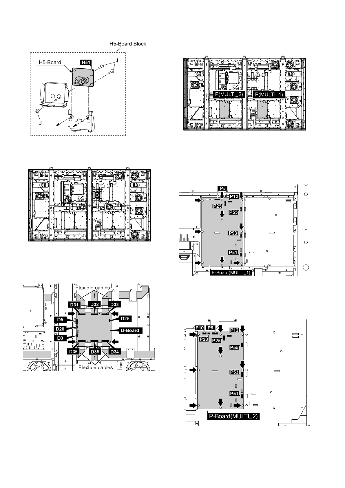
7.10. Removal of H5-Board
1. Disconnect a connector (H51).
2. Remove 2 screws and then remove H5-Board Block.
29
TH-103PF10WK/TK/RK
3. Remove 3 screws (J) and then remove H5-Board.
7.11. Removal of D-Board
7.12. Removal of P-Board (MULTI_1),
(MULTI_2)
The fuses are not included in P-Board for the repair.
7.12.1. Removal of P-Board (MULTI_1)
1. Disconnect the connectors (P5, P12, P25, P51, P53,
P55).
2. Remove 9 screws and then remove P-Board (MULTI_1).
1. Remove the flexible cables from the connectors (D31,
D32, D33, D34, D35, D36).
2. Disconnect the connectors (D3, D5, D20, D25).
3. Remove 4 screws and then remove D-Board.
7.12.2. Removal of P-Board (MULTI_2)
1. Disconnect the connectors (P5, P10, P12, P23, P25, P51,
P53, P55).
2. Remove 9 screw and then remove P-Board (MULTI_2).
30
 Loading...