

Page 1
ORDER NO.MTNC100556CE
B34 Canada: B62
58 inch Class 1080p Plasma HDTV
Model No. TC-P58VT25
GPF13DU Chassis
© Panasonic Corporation 2010.
Unauthorized copying and distribution is a violation
of law.
Page 2

TABLE OF CONTENTS
1 Safety Precautions --------------------------------------------------------------3
1.1. General Guidelines -----------------------------------------------------3
2Warning----------------------------------------------------------------------------- 4
2.1. Prevention of Electrostatic Discharge (ESD) to
Electrostatically Sensitive (ES) Devices---------------------------
2.2. About lead free solder (PbF) ----------------------------------------- 5
3 Service Navigation --------------------------------------------------------------6
3.1. PCB Layout--------------------------------------------------------------- 6
3.2. Applicable signals-------------------------------------------------------7
4 Specifications---------------------------------------------------------------------8
5 Service Mode----------------------------------------------------------------------9
5.1. How to enter into Service Mode-------------------------------------9
5.2. Option - Mirror----------------------------------------------------------11
5.3. Service tool mode ----------------------------------------------------- 11
5.4. Hotel mode--------------------------------------------------------------12
5.5. Data Copy by SD Card ----------------------------------------------13
6 Troubleshooting Guide ------------------------------------------------------16
6.1. Check of the IIC bus lines-------------------------------------------16
6.2. Power LED Blinking timing chart----------------------------------17
6.3. No Power----------------------------------------------------------------18
6.4. No Picture---------------------------------------------------------------19
6.5. Local screen failure---------------------------------------------------20
7 Service Fixture & Tools------------------------------------------------------21
7.1. SC jig---------------------------------------------------------------------21
8 Disassembly and Assembly Instructions------------------------------22
8.1. Remove the Rear cover ---------------------------------------------22
8.2. Remove the AC inlet -------------------------------------------------22
8.3. Remove the P-Board-------------------------------------------------22
8.4. Remove the Side terminal cover and the Rear AV panel----22
8.5. Remove the Tuner unit-----------------------------------------------23
8.6. Remove the A-Board-------------------------------------------------23
8.7. Remove the Speakers -----------------------------------------------23
8.8. Remove the Woofer box---------------------------------------------23
8.9. Remove the SU-Board-----------------------------------------------24
8.10. Remove the SD-Board-----------------------------------------------24
8.11. Remove the SC-Board-----------------------------------------------24
8.12. Remove the SS2-Board ---------------------------------------------24
8.13. Remove the SS-Board-----------------------------------------------25
8.14. Remove the Support metal -----------------------------------------25
8.15. Remove the Hanger metals and the Stand brackets---------25
8.16. Remove the D-Board-------------------------------------------------26
8.17. Remove the C1-Board----------------------------------------------- 26
8.18. Remove the C2-Board----------------------------------------------- 26
8.19. Remove the C3-Board----------------------------------------------- 26
8.20. Remove the C4-Board----------------------------------------------- 27
8.21. Remove the C5-Board----------------------------------------------- 27
8.22. Remove the C6-Board----------------------------------------------- 27
8.23. Remove the Plasma panel section from the Cabinet
assy-----------------------------------------------------------------------
8.24. Remove the Contact metals----------------------------------------28
8.25. Remove the K-Board-------------------------------------------------29
8.26. Remove the V-Board-------------------------------------------------29
8.27. Replace the plasma panel ------------------------------------------29
9 Measurements and Adjustments-----------------------------------------30
9.1. Adjustment--------------------------------------------------------------30
10 Block Diagram ------------------------------------------------------------------35
10.1. Main Block Diagram--------------------------------------------------35
10.2. Block (1/5) Diagram --------------------------------------------------36
10.3. Block (2/5) Diagram --------------------------------------------------37
10.4. Block (3/5) Diagram --------------------------------------------------38
10.5. Block (4/5) Diagram --------------------------------------------------39
10.6. Block (5/5) Diagram --------------------------------------------------40
11 Wiring Connection Diagram------------------------------------------------41
11.1. Caution statement.----------------------------------------------------41
11.2. Wiring (1)----------------------------------------------------------------41
11.3. Wiring (2)----------------------------------------------------------------41
11.4. Wiring (3)----------------------------------------------------------------42
11.5. Wiring (4)----------------------------------------------------------------43
11.6. Wiring (5)----------------------------------------------------------------44
11.7. Wiring (6)----------------------------------------------------------------45
PAGE PAGE
11.8. Wiring (7)--------------------- ------------------------------------------- 46
12 Schematic Diagram----------------------------------------------------------- 47
12.1. Schematic Diagram Note-------------------------------------------47
4
28
12.2. P(MAIN)-Board (1/3) Schematic Diagram----------------------48
12.3. P(MAIN)-Board (2/3) Schematic Diagram----------------------49
12.4. P(MAIN)-Board (3/3) Schematic Diagram----------------------50
12.5. P(SUB)-Board Schematic Diagram ------------------------------51
12.6. A-Board (1/20) Schematic Diagram------------------------------52
12.7. A-Board (2/20) Schematic Diagram------------------------------53
12.8. A-Board (3/20) Schematic Diagram------------------------------54
12.9. A-Board (4/20) Schematic Diagram------------------------------55
12.10. A-Board (5/20) Schematic Diagram------------------------------56
12.11. A-Board (6/20) Schematic Diagram------------------------------ 57
12.12. A-Board (7/20) Schematic Diagram------------------------------58
12.13. A-Board (8/20) Schematic Diagram------------------------------59
12.14. A-Board (9/20) Schematic Diagram------------------------------60
12.15. A-Board (10/20) Schematic Diagram----------------------------61
12.16. A-Board (11/20) and K-Board Schematic Diagram----------- 62
12.17. A-Board (12/20) Schematic Diagram----------------------------63
12.18. A-Board (13/20) Schematic Diagram----------------------------64
12.19. A-Board (14/20) Schematic Diagram----------------------------65
12.20. A-Board (15/20) and V-Board Schematic Diagram-----------66
12.21. A-Board (16/20) Schematic Diagram----------------------------67
12.22. A-Board (17/20) Schematic Diagram----------------------------68
12.23. A-Board (18/20) Schematic Diagram----------------------------69
12.24. A-Board (19/20) Schematic Diagram----------------------------70
12.25. A-Board (20/20) Schematic Diagram----------------------------71
12.26. D-Board (1/5) Schematic Diagram ------------------------------- 72
12.27. D-Board (2/5) Schematic Diagram ------------------------------- 73
12.28. D-Board (3/5) Schematic Diagram ------------------------------- 74
12.29. D-Board (4/5) Schematic Diagram ------------------------------- 75
12.30. D-Board (5/5) Schematic Diagram ------------------------------- 76
12.31. C1-Board Schematic Diagram---------------------- --------------- 77
12.32. C2-Board (1/2) Schematic Diagram------------------------------78
12.33. C2-Board (2/2) Schematic Diagram------------------------------79
12.34. C3-Board (1/2) Schematic Diagram------------------------------80
12.35. C3-Board (2/2) Schematic Diagram------------------------------81
12.36. C4-Board Schematic Diagram---------------------- --------------- 82
12.37. C5-Board (1/2) Schematic Diagram------------------------------83
12.38. C5-Board (2/2) Schematic Diagram------------------------------84
12.39. C6-Board (1/2) Schematic Diagram------------------------------85
12.40. C6-Board (2/2) Schematic Diagram------------------------------86
12.41. SC-Board (1/4) Schematic Diagram -----------------------------87
12.42. SC-Board (2/4) Schematic Diagram -----------------------------88
12.43. SC-Board (3/4) Schematic Diagram -----------------------------89
12.44. SC-Board (4/4) Schematic Diagram -----------------------------90
12.45. SS-Board (1/2) Schematic Diagram------------------------------91
12.46. SS-Board (2/2) and SS2-Board Schematic Diagram-------- 92
13 Printed Circuit Board--------------------------------------------------------- 93
13.1. P(MAIN)-Board --------------------------------------------------------93
13.2. P(SUB)-Board ---------------------------------------------------------96
13.3. K, V and SS2-Board--------------------------------------------------98
13.4. A-Board------------------------------------------------------------------ 99
13.5. D-Board ---------------------------------------------------------------101
13.6. C1-Board-------------------------------------------------------------- 103
13.7. C2-Board-------------------------------------------------------------- 104
13.8. C3-Board-------------------------------------------------------------- 105
13.9. C4-Board-------------------------------------------------------------- 106
13.10. C5-Board-------------------------------------------------------------- 107
13.11. C6-Board-------------------------------------------------------------- 108
13.12. SC-Board -------------------------------------------------------------109
13.13. SS-Board---------------------------------------------------------------111
14 Exploded View and Replacement Parts List------------------------ 113
14.1. Exploded View and Mechanical Replacement Parts List - 113
14.2. Electrical Replacement Parts List------------------------------- 119
2
Page 3
1 Safety Precautions
1.1. General Guidelines
1. When conducting repairs and servicing, do not attempt to modify the equipment, its parts or its materials.
2. When wiring units (with cables, flexible cables or lead wires) are supplied as repair parts and only one wire or some of the
wires have been broken or disconnected, do not attempt to repair or re-wire the units. Replace the entire wiring unit instead.
3. When conducting repairs and servicing, do not twist the Fasten connectors but plug them straight in or unplug them straight
out.
4. When servicing, observe the original lead dress. If a short circuit is found, replace all parts which have been overheated or
damaged by the short circuit.
5. After servicing, see to it that all the protective devices such as insulation barriers, insulation papers shields are properly
installed.
6. After servicing, make the following leakage current checks to prevent the customer from being exposed to shock hazards.
1.1.1. Leakage Current Cold Check
1. Unplug the AC cord and connect a jumper between the
two prongs on the plug.
2. Measure the resistance value, with an ohmmeter,
between the jumpered AC plug and each exposed metallic cabinet part on the equipment such as screwheads,
connectors, control shafts, etc. When the exposed metallic part has a return path to the chassis, the reading
should be between 1Mohm and 5.2Mohm.
When the exposed metal does not have a return path to
the chassis, the reading must be .
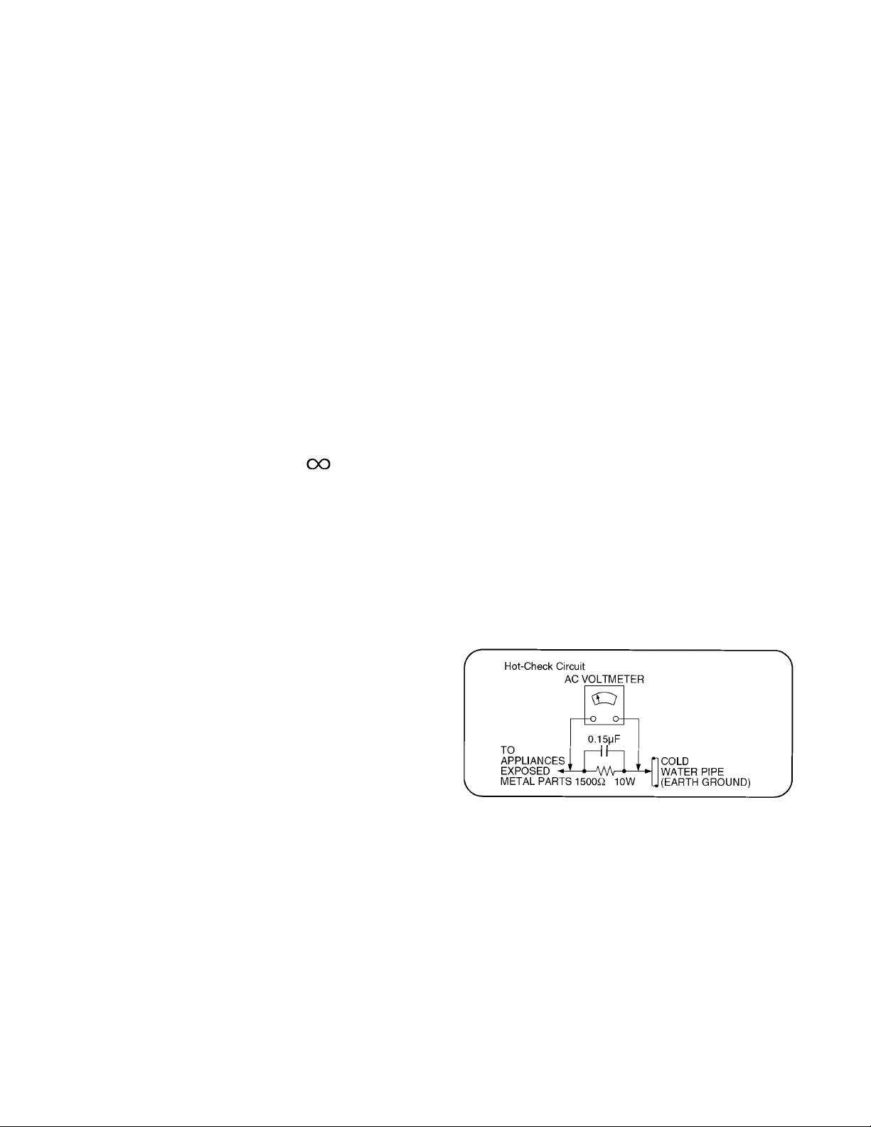
1.1.2. Leakage Current Hot Check (See Figure 1.)
1. Plug the AC cord directly into the AC outlet. Do not use
an isolation transformer for this check.
2. Connect a 1.5kohm, 10 watts resistor, in parallel with a
0.15μF capacitors, between each exposed metallic part
on the set and a good earth ground such as a water pipe,
as shown in Figure 1.
3. Use an AC voltmeter, with 1000 ohms/volt or more sensitivity, to measure the potential across the resistor.
4. Check each exposed metallic part, and measure the voltage at each point.
5. Reverse the AC plug in the AC outlet and repeat each of
the above measurements.
6. The potential at any point should not exceed 0.75 volts
RMS. A leakage current tester (Simpson Model 229 or
equivalent) may be used to make the hot checks, leakage
current must not exceed 1/2 milliamp. In case a measurement is outside of the limits specified, there is a possibility
of a shock hazard, and the equipment should be repaired
and rechecked before it is returned to the customer.
Figure 1
3
Page 4

2 Warning
2.1. Prevention of Electrostatic Discharge (ESD) to Electrostatically Sensitive (ES) Devices
Some semiconductor (solid state) devices can be damaged easily by static electricity. Such components commonly are called Electrostatically Sensitive (ES) Devices. Examples of typical ES devices are integrated circuits and some field-effect transistors and
semiconductor [chip] components. The following techniques should be used to help reduce the incidence of component damage
caused by electrostatic discharge (ESD).
1. Immediately before handling any semiconductor component or semiconductor-equipped assembly, drain off any ESD on your
body by touching a known earth ground. Alternatively, obtain and wear a commercially available discharging ESD wrist strap,
which should be removed for potential shock reasons prior to applying power to the unit under test.
2. After removing an electrical assembly equipped with ES devices, place the assembly on a conductive surface such as aluminum foil, to prevent electrostatic charge buildup or exposure of the assembly.
3. Use only a grounded-tip soldering iron to solder or unsolder ES devices.
4. Use only an anti-static solder removal device. Some solder removal devices not classified as [anti-static (ESD protected)] can
generate electrical charge sufficient to damage ES devices.
5. Do not use freon-propelled chemicals. These can generate electrical charges sufficient to damage ES devices.
6. Do not remove a replacement ES device from its protective package until immediately before you are ready to install it. (Most
replacement ES devices are packaged with leads electrically shorted together by conductive foam, aluminum foil or comparable conductive material).
7. Immediately before removing the protective material from the leads of a replacement ES device, touch the protective material
to the chassis or circuit assembly into which the device will be installed.
Caution
Be sure no power is applied to the chassis or circuit, and observe all other safety precautions.
8. Minimize bodily motions when handling unpackaged replacement ES devices. (Otherwise ham less motion such as the brushing together of your clothes fabric or the lifting of your foot from a carpeted floor can generate static electricity (ESD) sufficient
to damage an ES device).
4
Page 5
2.2. About lead free solder (PbF)
Note: Lead is listed as (Pb) in the periodic table of elements.
In the information below, Pb will refer to Lead solder, and PbF will refer to Lead Free Solder.
The Lead Free Solder used in our manufacturing process and discussed below is (Sn+Ag+Cu).
That is Tin (Sn), Silver (Ag) and Copper (Cu) although other types are available.
This model uses Pb Free solder in it’s manufacture due to environmental conservation issues. For service and repair work, we’d
suggest the use of Pb free solder as well, although Pb solder may be used.
PCBs manufactured using lead free solder will have the PbF within a leaf Symbol PbF stamped on the back of PCB.
Caution
• Pb free solder has a higher melting point than standard solder. Typically the melting point is 50 ~ 70 °F (30~40 °C) higher. Please
use a high temperature soldering iron and set it to 700 ± 20 °F (37 0 ± 10 °C).
• Pb free solder will tend to splash when heated too high (about 1100 °F or 600 °C).
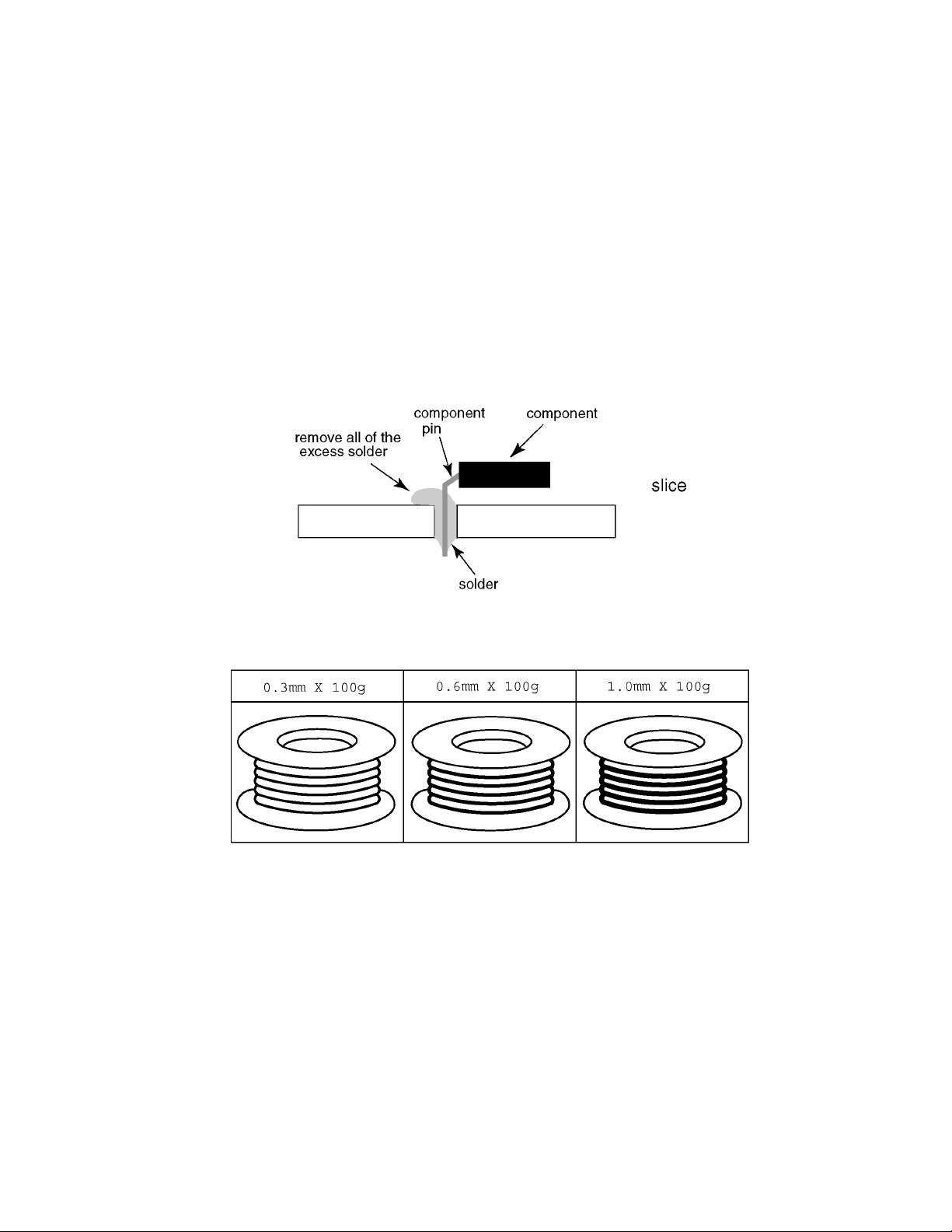
If you must use Pb solder, please completely remove all of the Pb free solder on the pins or solder area before applying Pb solder. If this is not practical, be sure to heat the Pb free solder until it melts, before applying Pb solder.
• After applying PbF solder to double layered boards, please check the component side for excess solder which may flow onto the
opposite side. (see figure below)
Suggested Pb free solder
There are several kinds of Pb free solder available for purchase. This product uses Sn+Ag+Cu (tin, silver, copper) solder. However, Sn+Cu (tin, copper), Sn+Zn+Bi (tin, zinc, bismuth) solder can also be used.
5
Page 6
3 Service Navigation
3.1. PCB Layout
Board Name Function Board Name Function
P Power Supply C1 Data Driver (Lower Right)
C2 Data Driver (Lower Center)
A DC-DC Converter, Tuner
Speaker out, AV Terminal, HDMI in, SD Card, PC in
Digital Signal Processor, PEAKS-LDA2
Power Switch, Key Switch
K Remote receiver, Power LED, C.A.T.S sensor SU Scan out (Upper)
V 3D Eyewear transmitter
D Format Converter, Plasma AI, Sub-Field Processor
C3 Data Driver (Lower Left)
C4 Data Driver (Upper Right)
C5 Data Driver (Upper Center)
C6 Data Driver (Upper Left)
SC Scan Drive
SS Sustain Drive
SS2 Sustain out (Lower)
Non serviceable.
SU-Board should be exchanged for service.
SD Scan out (Lower)
Non serviceable.
SD-Board should be exchanged for service.
6
Page 7
3.2. Applicable signals
* Mark: Applicable input signal for Component (Y, PB, PR), HDMI and PC
horizontal frequency (kHz) vertical frequency (Hz) COMPONENT HDMI PC
525 (480) / 60i 15.73 59.94 * *
525 (480) /60p 31.47 59.94 * *
750 (720) /60p 45.00 59.94 * *
1,125 (1,080) /60i 33.75 59.94 * *
1,125 (1,080) /60p 67.43 59.94 *
1,125 (1,080) /60p 67.50 60.00 *
1,125 (1,080) /24p 26.97 23.98 *
1,125 (1,080) /24p 27.00 24.00 *
640 × 400 @70 31.47 70.08 *
640 × 480 @60 31.47 59.94 *
Macintosh13 inch (640 × 480) 35.00 66.67 *
640 × 480 @75 37.50 75.00 *
852 × 480 @60 31.44 59.89 *
800 × 600 @60 37.88 60.32 *
800 × 600 @75 46.88 75.00 *
800 × 600 @85 53.67 85.08 *
Macintosh16 inch (832 × 624) 49.73 74.55 *
1,024 × 768 @60 48.36 60.00 *
1,024 × 768 @70 56.48 70.07 *
1,024 × 768 @75 60.02 75.03 *
1,024 × 768 @85 68.68 85.00 *
Macintosh 21 inch (1,152 ×870) 68.68 75.06 *
1,280 × 768 @60 47.78 59.87 *
1,280 × 1,024 @60 63.98 60.02 *
1,366 × 768 @60 48.39 60.04 *
Note
• Signals other than those shown above may not be displayed properly.
• The above signals are reformatted for optimal viewing on your display.
7
Page 8

4 Specifications
Power Source AC 120 V, 60 Hz
Power Consumption
Maximum 599 W
Standby condition 0.2 W
Plasma Display panel
Drive method AC type
Aspect Ratio 16:9
Visible screen size 58 inch class (58.0 inches measured diagonally)
(W × H × Diagonal) 50.5 inch × 28.4 inch × 58.0 inch (1,284 mm × 722 mm × 1,473 mm)
(No. of pixels) 2,073,600 (1,920 (W) × 1,080 (H)) [5,760 × 1,080 dots]
Sound
Audio Output 30 W [ 10 W + 10 W + 10 W ] ( 10 % THD )
PC signals VGA, SVGA, XGA, WXGA, SXGA
Horizontal scanning frequency 31 - 69 kHz
Vertical scanning frequency 59 - 86 Hz
Channel Capability (Digital/Analog) VHF/ UHF: 2 - 69, CATV: 1 - 135
Operating Conditions
Temperature: 32 °F - 104 °F (0 °C - 40 °C)
Humidity: 20 % - 80 % RH (non-condensing)
Connection Terminals
VIDEO IN 1-2 VIDEO: RCA PIN Type × 1 1.0 V [p-p] (75 Ω)
AUDIO L-R: RCA PIN Type × 2 0.5 V [rms]
COMPONENT IN 1-2 Y: 1.0 V [p-p] (including synchronization)
PB, PR: ±0.35 V [p-p]
AUDIO L-R: RCA PIN Type × 2 0.5 V [rms]
HDMI 1-4 TYPE A Connector × 4
This TV supports [HDAVI Control 5] function.
USB 1-2 USB 2.0 Type A connector x 2 (DC 5 V MAX 500 mA)
PC D-SUB 15PIN: R,G,B / 0.7 V [p-p] (75 Ω)
RS232C (Serial) D-sub 9pin for external control
LAN (for VIERA CAST IPTV) RJ45 (10BASE-T/100BASE-TX)
Card slot SD CARD slot × 1
DIGITAL AUDIO OUT PCM / Dolby Digital, Fiber Optic
FEATURES 3D Y/C FILTER
CLOSED CAPTION V-Chip
IPTV (VIERA CAST) Media player
VIERA IMAGE VIEWER HDAVI Control 5
Dimensions (W × H × D)
Including pedestal 56.3 inch ×
TV Set only 56.3 inch × 34.8 inch × 3.6 inch (1,430 mm × 884 mm × 90 mm)
Mass
Including pedestal 94.8 lb (43.0 kg)
TV Set only 88.2 lb (40.0 kg)
36.9 inch × 1
HD, VD / 1.0 - 5.0 V [p-p] (high impedance)
.3 inch (1,430 mm × 935mm × 387 mm)
5
Note
• Design and Specifications are subject to change without notice. Mass and Dimensions shown are approximate.
8
Page 9
5 Service Mode
5.1. How to enter into Service Mode
While pressing [VOLUME ( - )] button of the main unit, press [INFO] button of the remote control three times within 2 seconds
Note:
Service Mode can not be entered when 3D signal input.
Input 2D signal to enter Service Mode.
5.1.1. Key command
[1] button...Main items Selection in forward direction
[2] button...Main items Selection in reverse direction
[3] button...Sub items Selection in forward direction
[4] button...Sub items Selection in reverse direction
[VOL] button...Value of sub items change in forward direction ( + ), in reverse direction ( - )
9
Page 10
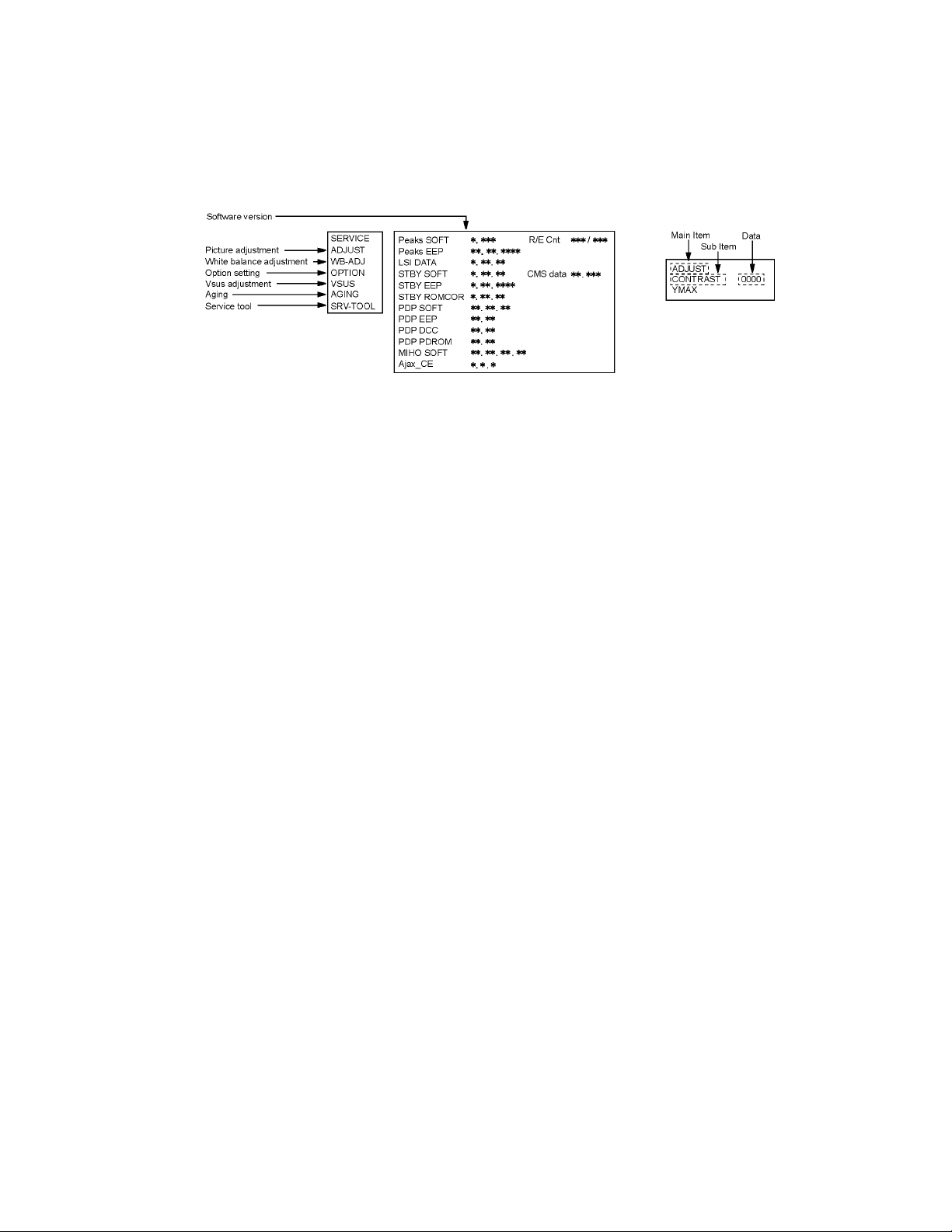
5.1.2. Contents of adjustment mode
• Value is shown as a hexadecimal number.
• Preset value differs depending on models.
• After entering the adjustment mode, take note of the value in each item before starting adjustment.
Main item Sub item Sample Data Remark
ADJUST CONTRAST 46
COLOR 00
TINT 00
SUB-BRT 000
WB-ADJ R-CUT 80
G-CUT 80
B-CUT 80
R-DRV FD
G-DRV FB
B-DRV FF
ALL-CUT 80
ALL-DRV FF
OPTION BOOT ROM Factory Preset
STBY-SET - EMERGENCY ON
CLK MODE ON
CLOCK FFF
EDID-CLK HIGH
MIRROR 00 (See next)
VSUS
AGING ALL WHITE Built-in test patterns can be
ALL BLUE WITH WHITE OUT-
SIDE FRAME
ALL GREEN
ALL RED
LOW STEP WHITE
LOW STEP BLUE
LOW STEP GREEN
LOW STEP RED
WHITE DIAGONAL STRIPE
RED DIAGONAL STRIPE
GREEN DIAGONAL STRIPE
BLUE DIAGONAL STRIPE
A-ZONE & B-ZONE
1% WINDOW
COLOR BAR
9 POINTS BRIGHT MEASURE
2 DOT OUTSIDE FRAME
ALL BLUE
DOUBLE FIXED 1% WINDOW
VERTICAL LINE SCROLL
ON/OFF OR WHITE
R/G/B/W ROTATION
HALF FIXED ALL WHITE
ALL WHITE WITH COUNT DIS-
PLAY
SRV-TOOL - See next
displayed.
5.1.3. How to exit
Switch off the power with the [POWER] button on the main unit or the [POWER] button on the remote control.
10
Page 11
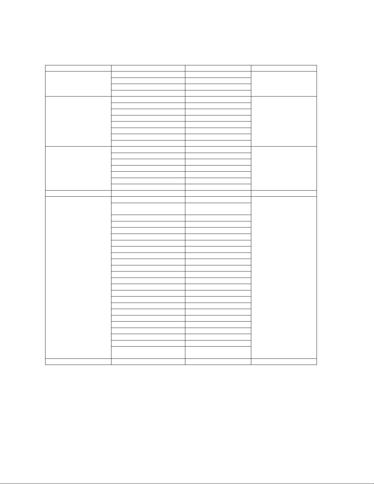
5.2. Option - Mirror
Picture can be reversed left and right or up and down.
00 : Default (Normal picture is displayed)
01 : Picture is reversed left and right.
02 : Picture is reversed up and down.
Hint : If the defective symptom (e.g. Vertical bar or Horizontal bar) is moved by selection of this mirror, the possible cause is in
A-board or D-board.
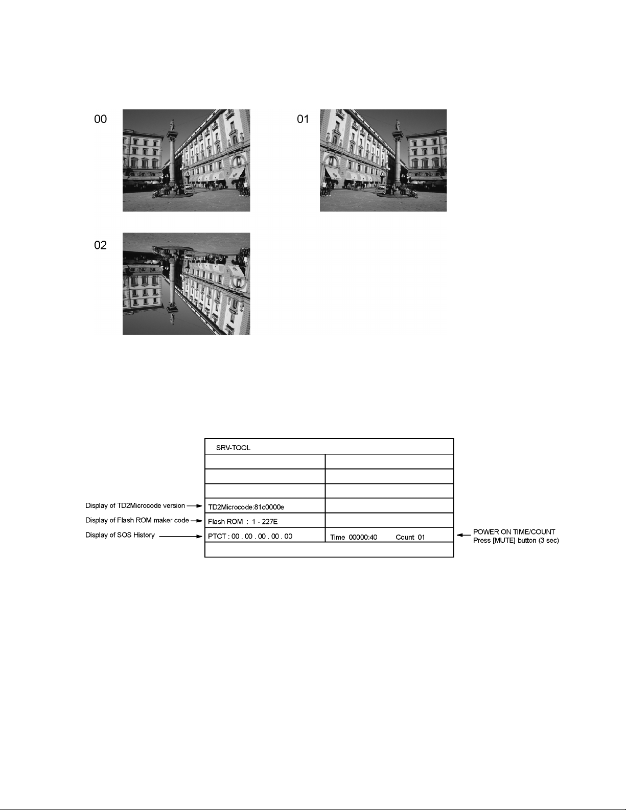
5.3. Service tool mode
5.3.1. How to access
1. Select [SRV-TOOL] in Service Mode.
2. Press [OK] button on the remote control.
5.3.2. Display of SOS History
SOS History (Number of LED blinking) indication.
From left side; Last SOS, before Last, three occurrence before, 2nd occurrence after shipment, 1st occurrence after shipment.
This indication except 2nd and 1st occurrence after shipment will be cleared by [Self-check indication and forced to factory shipment setting].
5.3.3. POWER ON TIME/COUNT
Note : To display TIME/COUNT menu, highlight position, then press MUTE for (3 sec).
Time : Cumulative power on time, indicated hour : minute by decimal
Count : Number of ON times by decimal
Note : This indication will not be cleared by either of the self-checks or any other command.
5.3.4. Exit
1. Disconnect the AC cord from wall outlet.
11
Page 12
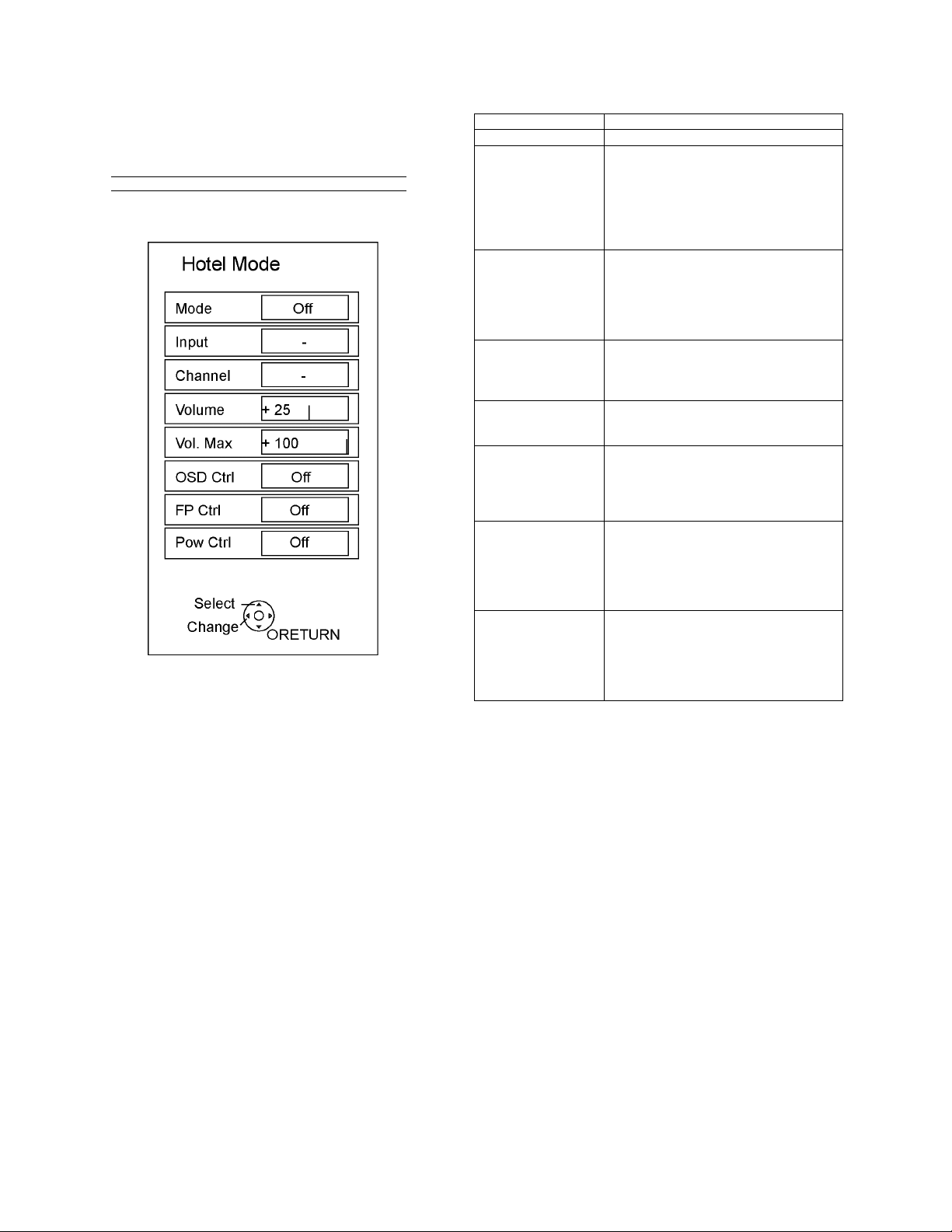
5.4. Hotel mode
1. Purpose
Restrict a function for hotels.
2. Access command to the Hotel mode setup menu
In order to display the Hotel mode setup menu, please
enter the following command (within 2 second).
[TV] : Vol. [Down] + [REMOTE] : INPUT (3 times)
Then, the Hotel mode setup menu is displayed.
3. To exit the Hotel mode setup menu
Disconnect AC power cord from wall outlet.
4. Explain the Hotel mode setup menu
item Function
Mode Select hotel mode ON/OFF
Input Select input signal modes.
Set the input, when each time power is
switched on.
Selection:
---/RF/HDMI1/HDMI2/HDMI3/HDMI4/
COMP1/COMP2/VIDEO1/VIDEO2/PC
• OFF: give priority to a last memory.
Channel Select channel when input signal is RF.
Set the channel, each time power is switched
on.
Selection:
Any channel number or [-].
[-] means the channel when turns off.
Volume Adjust the volume when each time p ower is
switched on.
Range:
0 to 100
Vol. Max Adjust maximum volume.
Range:
0 to 100
OSD Ctrl Restrict the OSD.
Selection:
OFF/PATTERN1
• OFF: No restriction
• PATTERN1: restriction
FP Ctrl Select front key conditions.
Selection:
OFF/ALL/PATTERN1
• OFF: altogether valid.
• ALL: altogether invalid.
• PATTERN1: only input key is valid.
Pow Ctrl Select POWER-ON/OFF con dition when AC
power cord is disconnected and then connected.
OFF: The same condition when AC power
cord is disconnected.
ON: Forced power ON condition.
12
Page 13
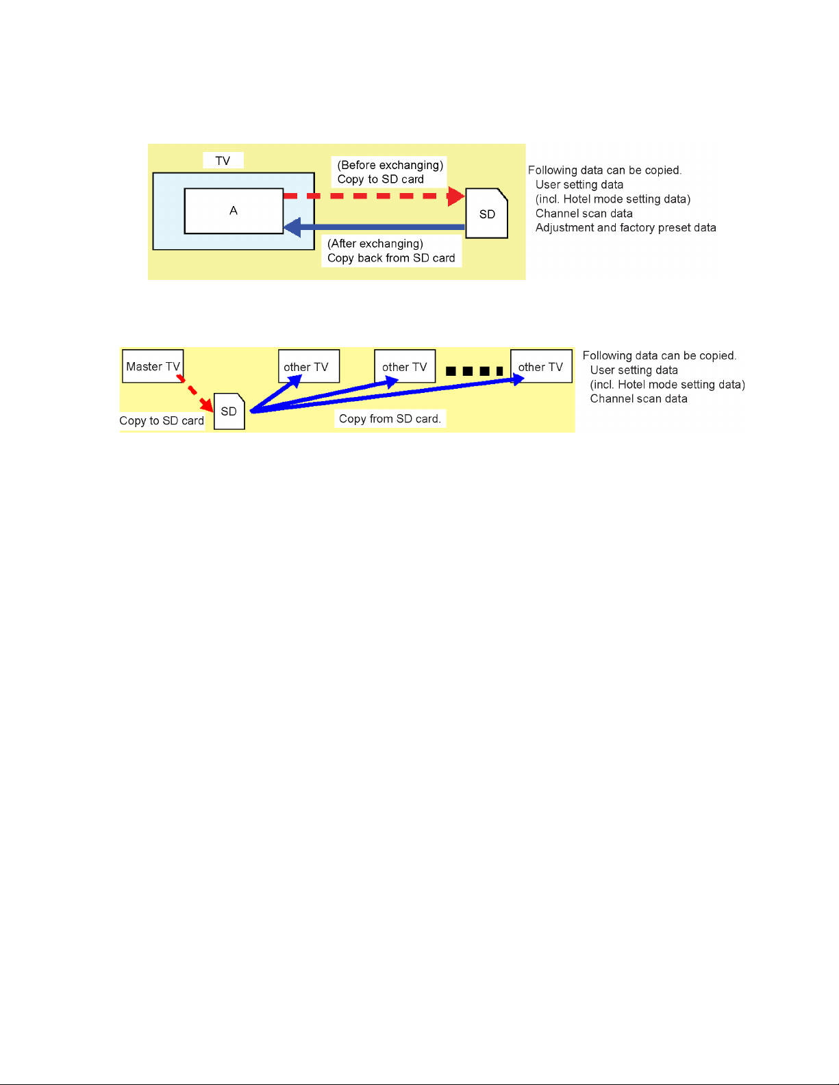
5.5. Data Copy by SD Card
5.5.1. Purpose
(a) Board replacement (Copy the data when exchanging A-board):
When exchanging A-board, the data in original A-board can be copied to SD card and then copy to new A-board.
(b) Hotel (Copy the data when installing a number of units in hotel or any facility):
When installing a number of units in hotel or any facility, the data in master TV can be copied to SD card and then copy to other
TVs.
5.5.2. Preparation
Make pwd file as startup file for (a) or (b) in a empty SD card.
1. Insert a empty SD card to your PC.
2. Right-click a blank area in a SD card window, point to New, and then click text document. A new file is created by default
(New Text Document.txt).
3. Right-click the new text document that you just created and select rename, and then change the name and extension of the
file to the following file name for (a) or (b) and press ENTER.
File name:
(a) For Board replacement : boardreplace.pwd
(b) For Hotel : hotel.pwd
Note:
Please make only one file to prevent the operation error.
No any other file should not be in SD card.
13
Page 14
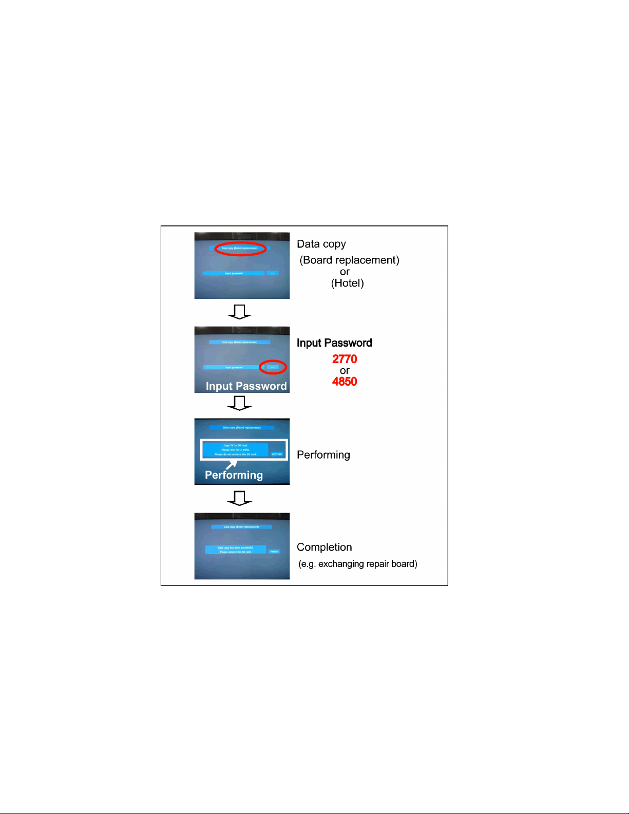
5.5.3. Data copy from TV set to SD Card
1. Turn on the TV set.
2. Insert SD card with a startup file (pwd file) to SD slot.
On-screen Display will be appeared according to the startup file automatically.
3. Input a following password for (a) or (b) by using remote control.
(a) For Board replacement : 2770
(b) For Hotel : 4850
Data will be copied from TV set to SD card.
It takes around 2 to 6 minutes maximum for copying.
4. After the completion of copying to SD card, remove SD card from TV set.
5. Turn off the TV set.
Note:
Following new folder will be created in SD card for data from TV set.
(a) For Board replacement : user_setup
(b) For Hotel : hotel
14
Page 15
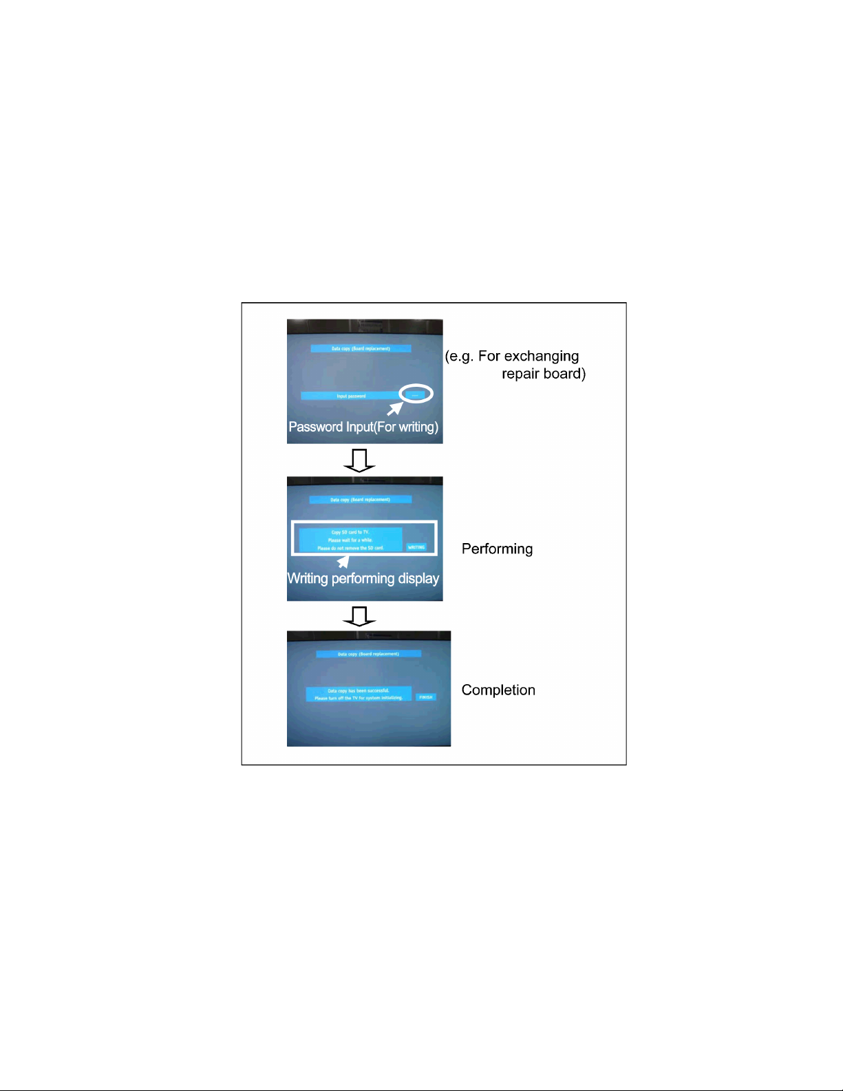
5.5.4. Data copy from SD Card to TV set
1. Turn on the TV set.
2. Insert SD card with Data to SD slot.
On-screen Display will be appeared according to the Data folder automatically.
3. Input a following password for (a) or (b) by using remote control.
(a) For Board replacement : 2771
(b) For Hotel : 4851
Data will be copied from SD card to TV set.
4. After the completion of copying to SD card, remove SD card from TV set.
(a) For Board replacement : Data will be deleted after copying (Limited one copy).
(b) For Hotel : Data will not be deleted and can be used for other TVs.
5. Turn off the TV set.
Note:
1. Depending on the failure of boards, function of Data copy for board replacement does not work.
2. This function can be effective among the same model numbers.
15
Page 16
6 Troubleshooting Guide
Use the self-check function to test the unit.
1. Checking the IIC bus lines
2. Power LED Blinking timing
6.1. Check of the IIC bus lines
6.1.1. How to access
6.1.1.1. Self-check indication only:
Produce TV reception screen, and while pressing [VOLUME ( - )] button on the main unit, press [OK] button on the remote control
for more than 3 seconds.
6.1.1.2. Self-check indication and forced to factory shipment setting:
Produce TV reception screen, and while pressing [VOLUME ( - )] button on the main unit, press [MENU] button on the remote control for more than 3 seconds.
6.1.2. Exit
Disconnect the AC cord from wall outlet.
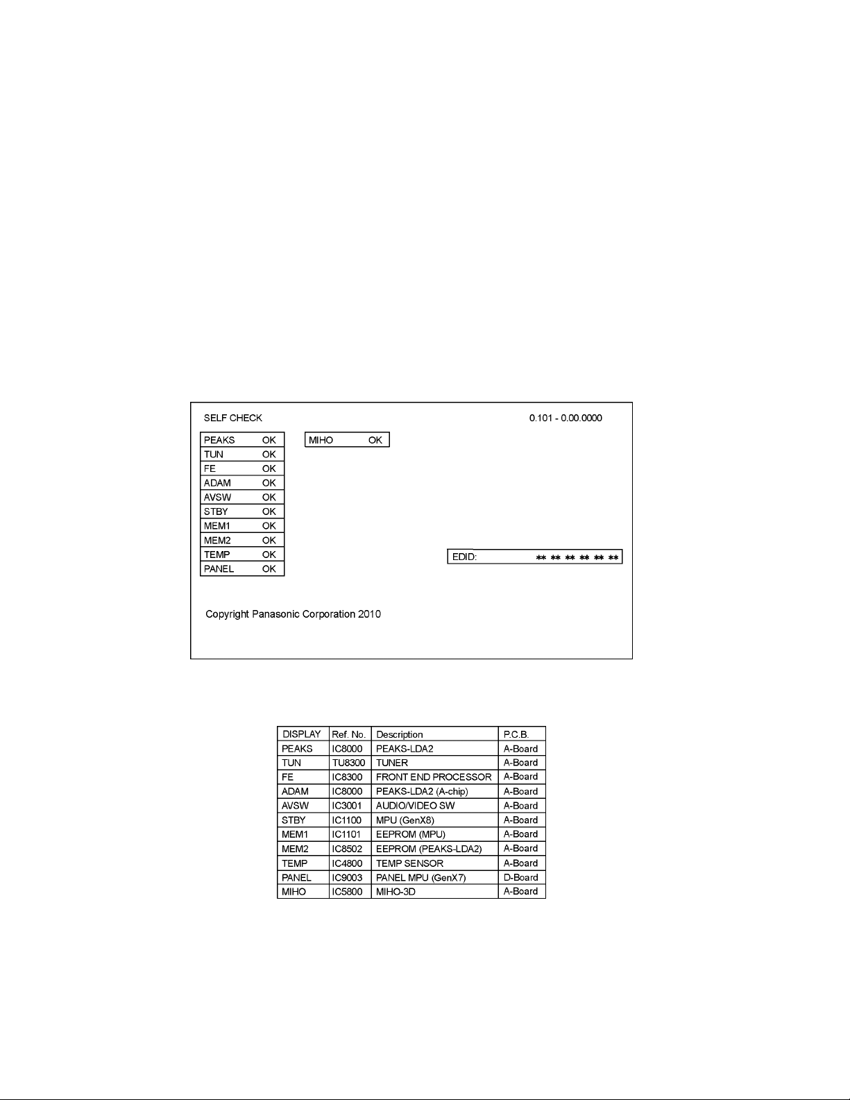
6.1.3. Screen display
6.1.4. Check Point
Confirm the following parts if NG was displayed.
16
Page 17
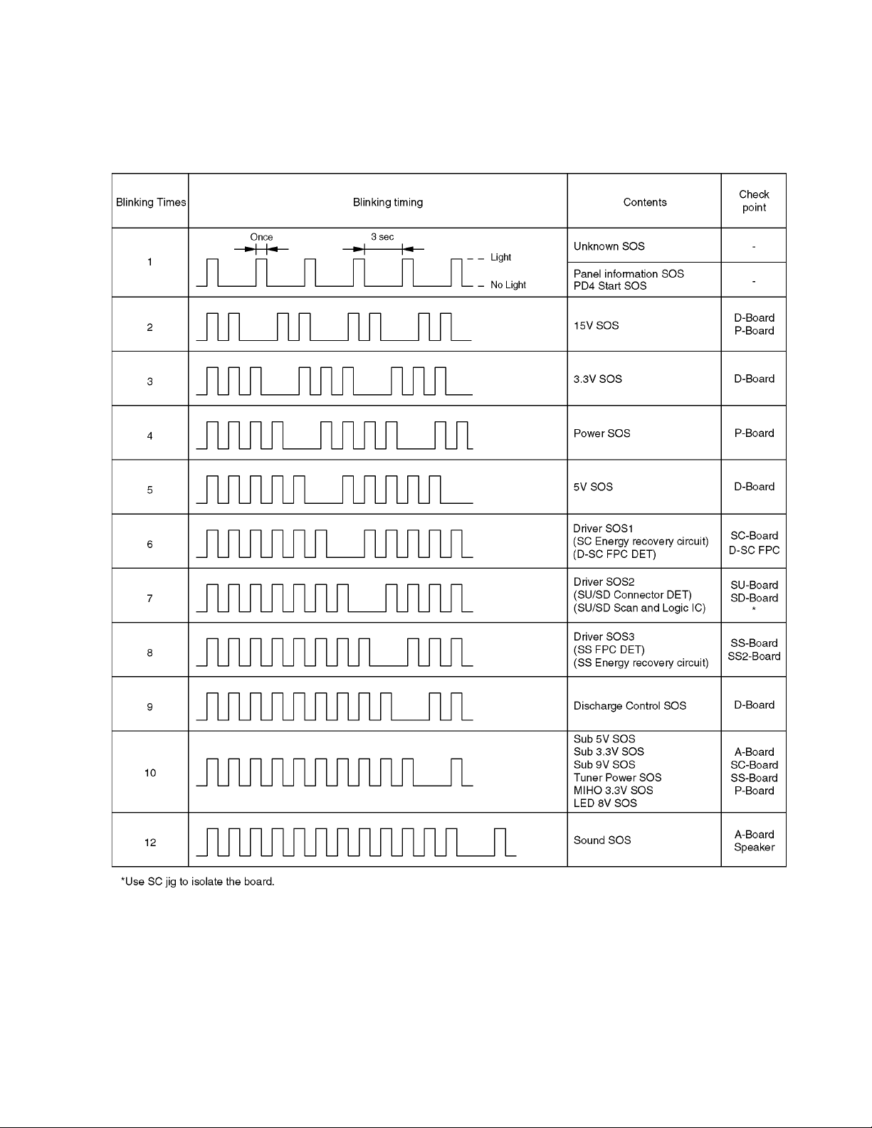
6.2. Power LED Blinking timing chart
1. Subject
Information of LED Flashing timing chart.
2. Contents
When an abnormality has occurred the unit, the protection circuit operates and reset to the stand by mode. At this time, the
defective block can be identified by the number of blinks of the Power LED on the front panel of the unit.
17
Page 18
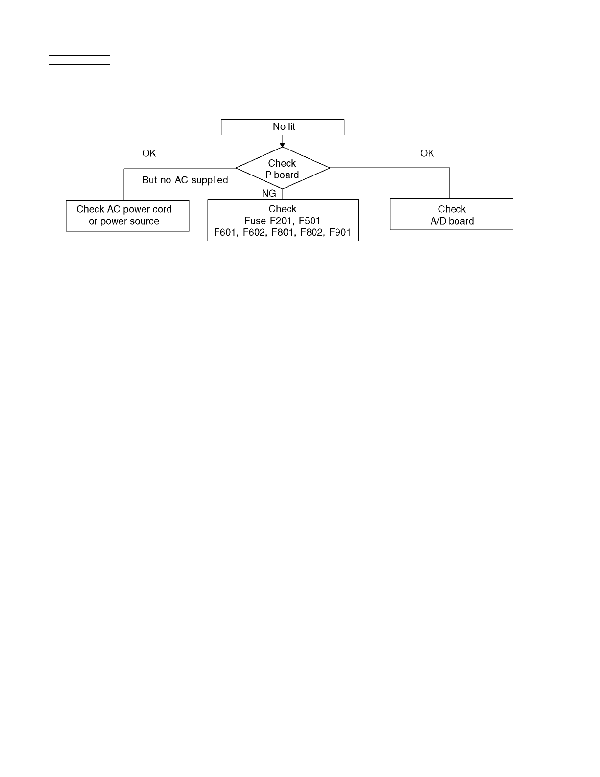
6.3. No Power
First check point
There are following 2 states of No Power indication by power LED.
1. No lit.
2. Red is lit then turns red blinking a few seconds later. (See 6.2.)
18
Page 19
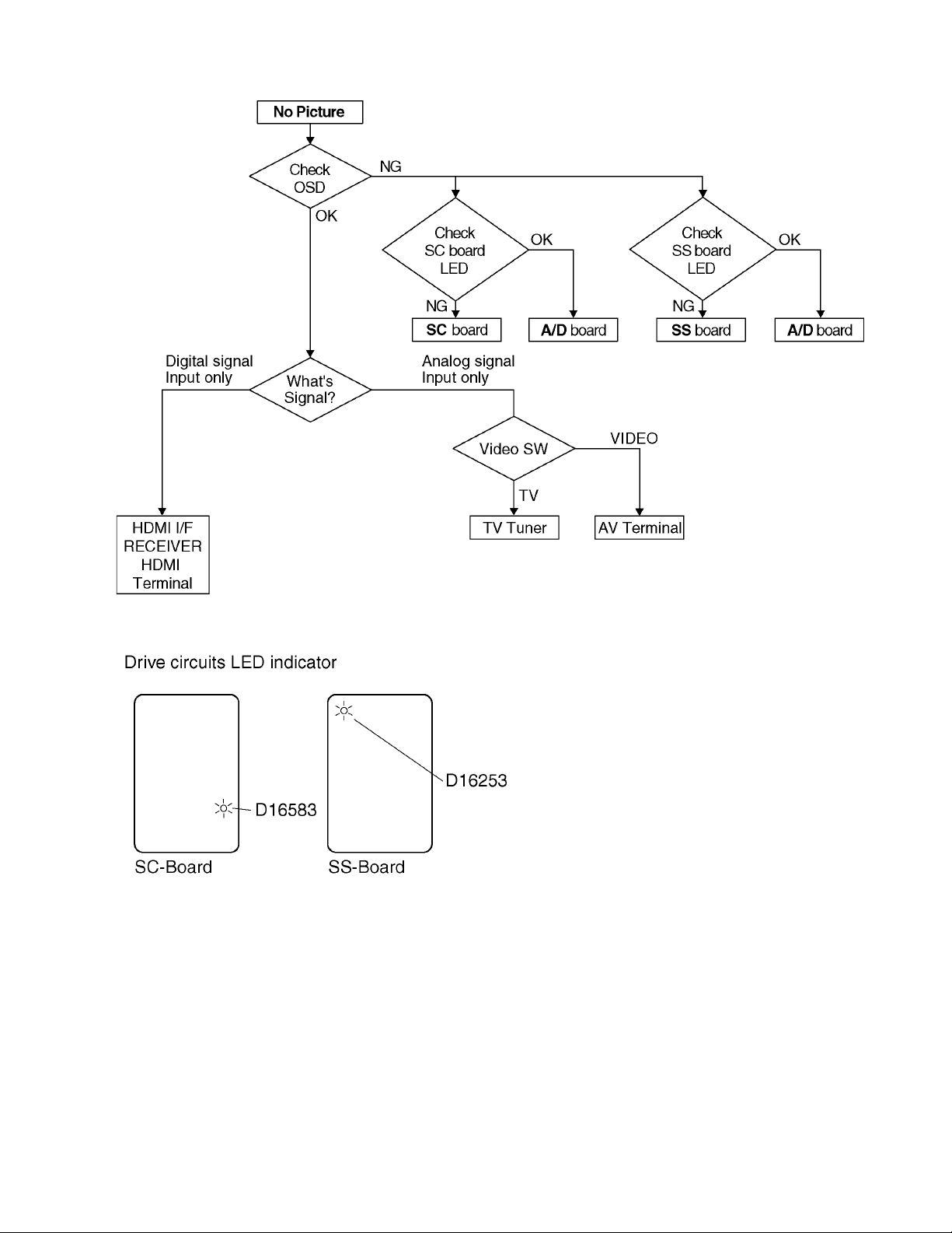
6.4. No Picture
19
Page 20
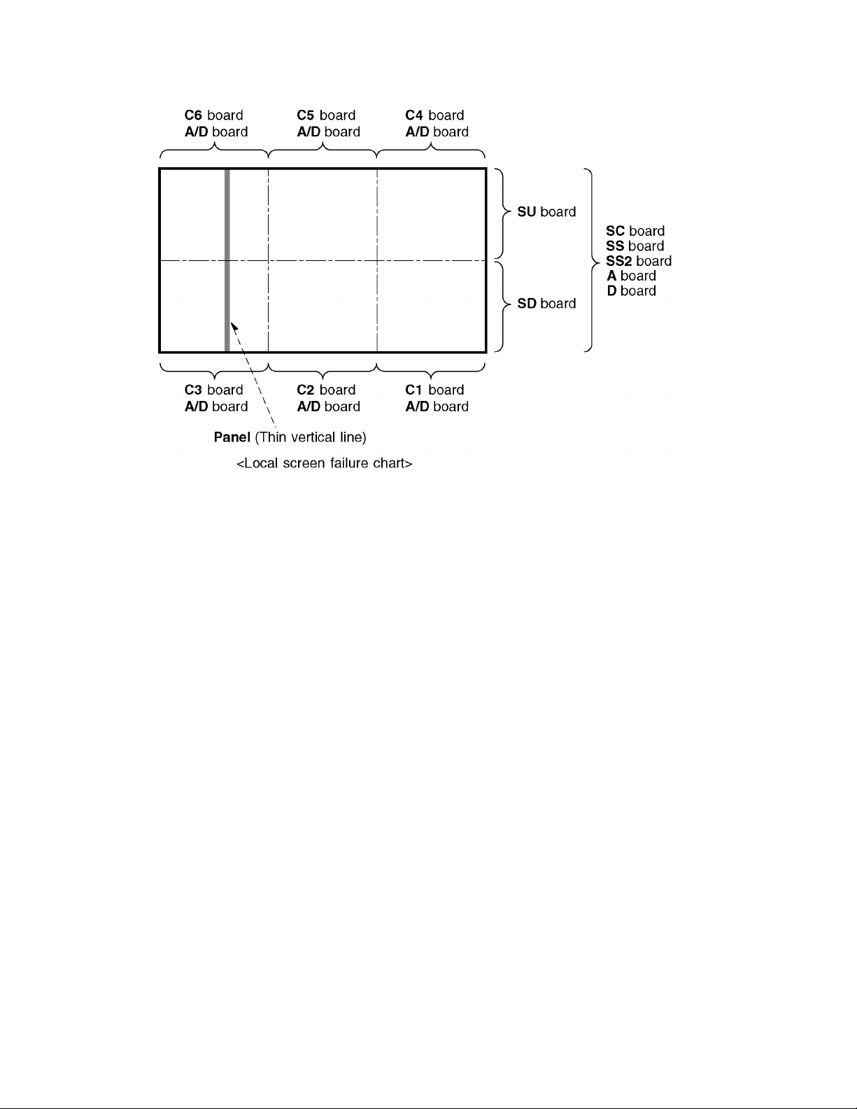
6.5. Local screen failure
Plasma display may have local area failure on the screen. Fig-1 is the possible defect P.C.B. for each local area.
Fig-1
20
Page 21
7 Service Fixture & Tools
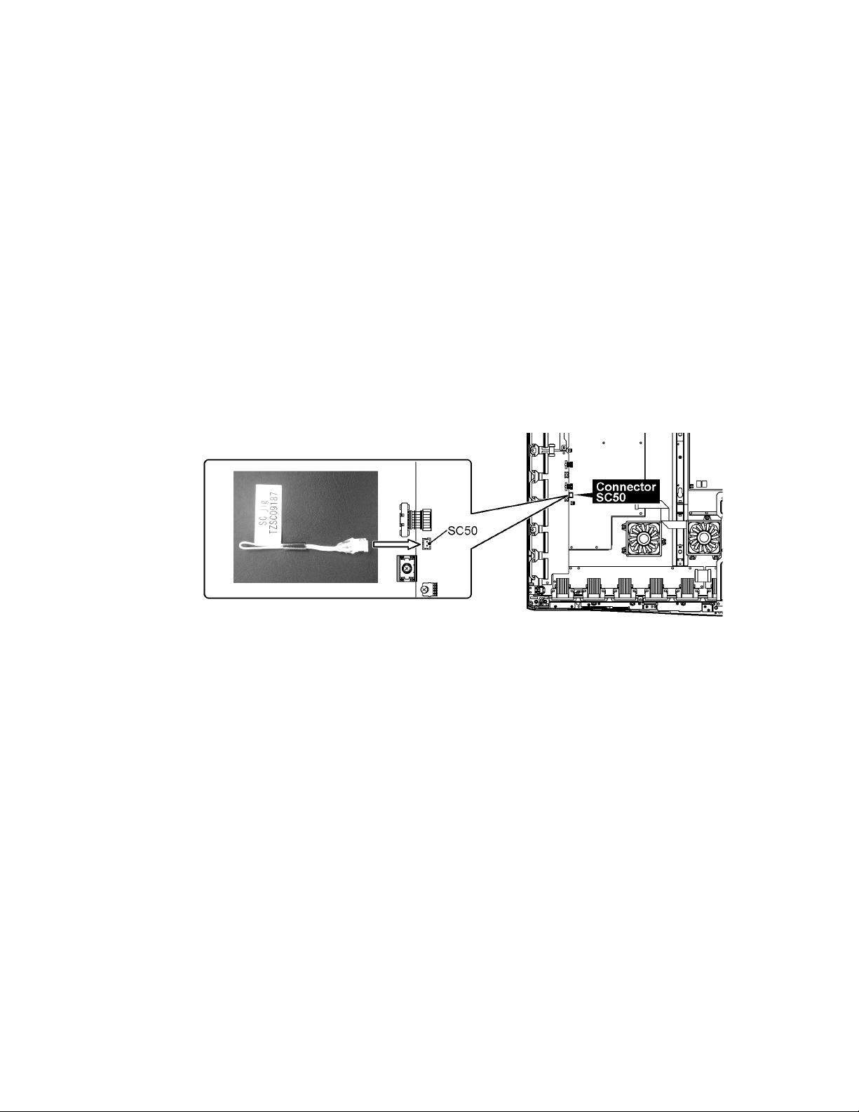
7.1. SC jig
Purpose:
To find the failure board (SC or SU/SD) when the power LED is blinking 7 times.
SC jig:
Jumper connector to connect to SC50 connector on SC board
Part number:
TZSC09187
How to use:
Caution: Remove SC jig from SC board after inspection.
1. Remove all connector between SC board and SU/SD board to isolate SC board from both SU and SD board electrically.
Note: The board will be damaged if all connector is not removed (for example; remove connector only for SU b oard and s tay
connecting with SD board. The board will be damaged.)
2. Connect SC jig to connector SC50 at left bottom side of SC board
3. Turn on the TV/Display Unit and confirm the power LED blinking.
LED blinking: Possible cause of failure is in SC board
No LED blinking (Lighting or no lighting): Possible cause of failure is in SU or SD board
4. After inspection, turn off the TV/Display Unit and wait a few minutes to discharge.
5. Remove SC jig from SC board.
Remark: This SC jig can be used for all 2010 Plasma TV and Plasma Display.
21
Page 22
8 Disassembly and Assembly Instructions
8.1. Remove the Rear cover
1. See PCB Layout (Section 3)
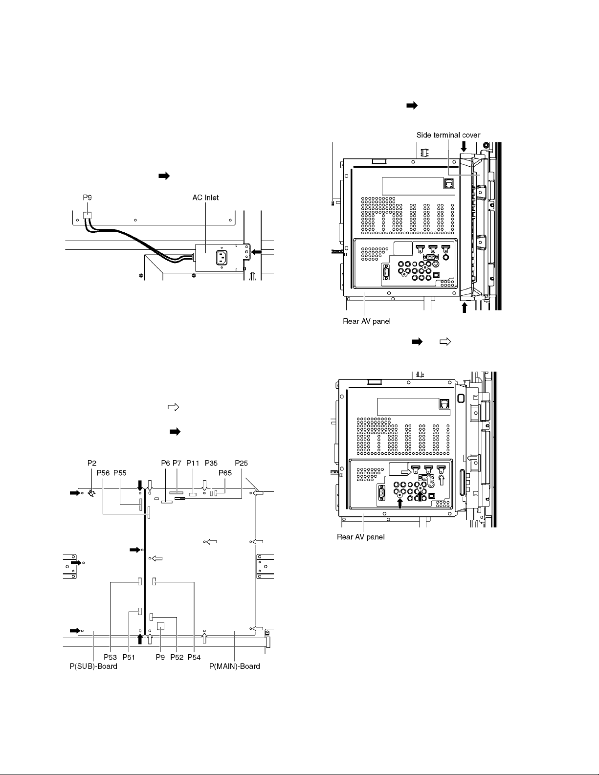
8.2. Remove the AC inlet
Caution:
To remove P.C.B. wait 1 minute after power was off for discharge from electrolysis capacitors.
1. Unlock the cable clampers to free the cable.
2. Disconnect the connector (P9).
3. Remove the screw (×1 ) and remove the AC inlet.
8.3. Remove the P-Board
Caution:
To remove P.C.B. wait 1 minute after power was off for discharge from electrolysis capacitors.
1. Unlock the cable clampers to free the cable.
2. Disconnect the connectors (P51-P52, P53-P54 and P55P56).
3. Disconnect the connectors (P2, P6, P7, P9, P11, P25,
P35 and P65).
4. Remove the screws (×9 ) and remove the P(MAIN)Board.
5. Remove the screws (×6 ) and remove the P(SUB)Board.
8.4. Remove the Side terminal cover and the Rear AV panel
1. Remove the claws (×2 ).
2. Remove the Side terminal cover.
3. Remove the screws (×2 , ×4 ).
4. Remove the Rear AV panel.
22
Page 23
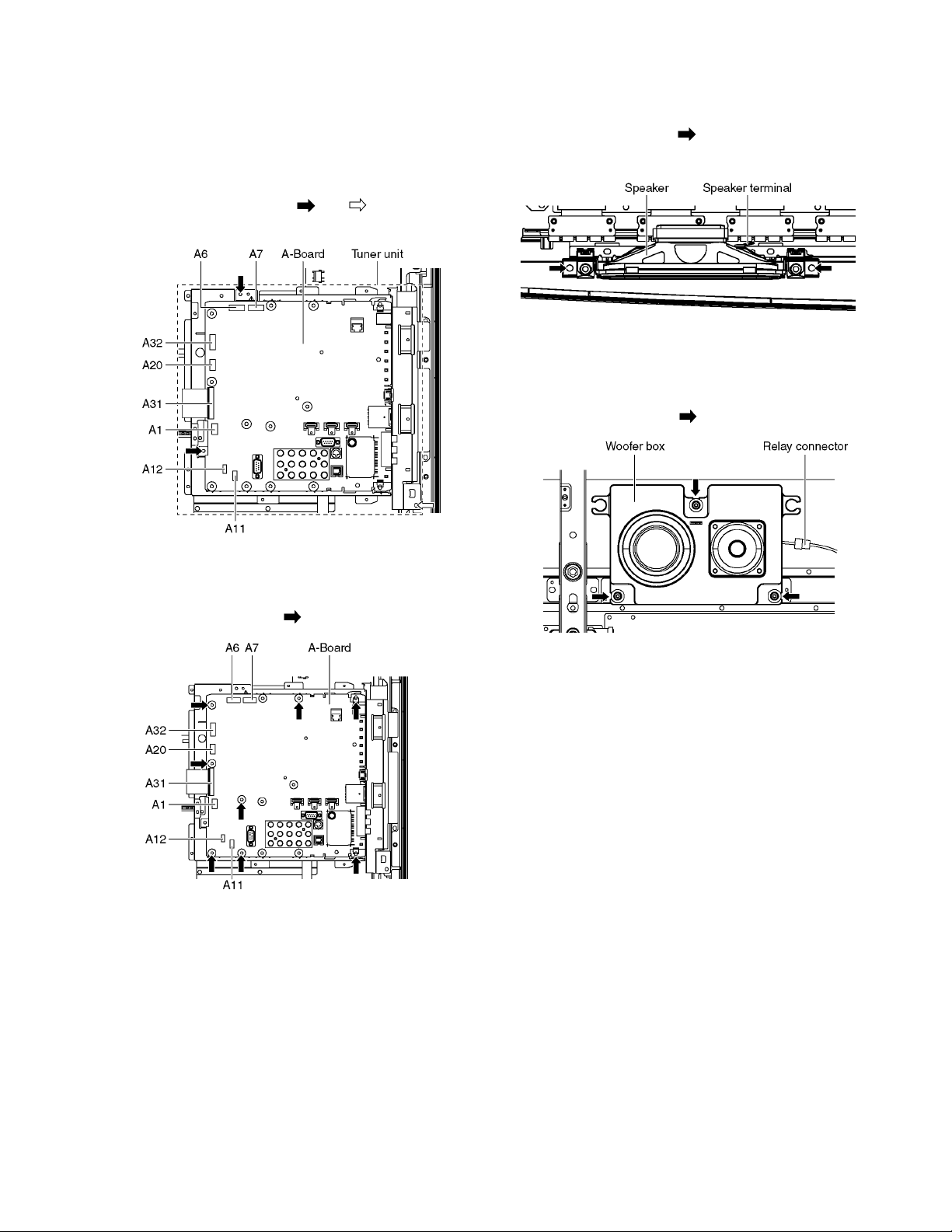
8.5. Remove the Tuner unit
1. Remove the Side terminal cover and the Rear AV panel.
(See section 8.4.)
2. Unlock the cable clampers to free the cable.
3. Disconnect the connectors (A1, A6, A7, A11, A12, A20
and A32).
4. Disconnect the flexible cable (A31).
5. Remove the screws (×2 , ×1 ) and remove the
Tuner unit.
8.7. Remove the Speakers
1. Unlock the cable clampers to free the cable.
2. Disconnect the Speaker terminal.
3. Remove the screws (×2 each) and remove the Speakers (L, R).
8.8. Remove the Woofer box
1. Unlock the cable clampers to free the cable.
2. Disconnect the Relay connector.
3. Remove the screws (×3 ) and remove the Woofer
box
.
8.6. Remove the A-Board
1. Remove the Tuner unit. (See section 8.5.)
2. Remove the screws (×8 ) and remove the A-Board.
23
Page 24
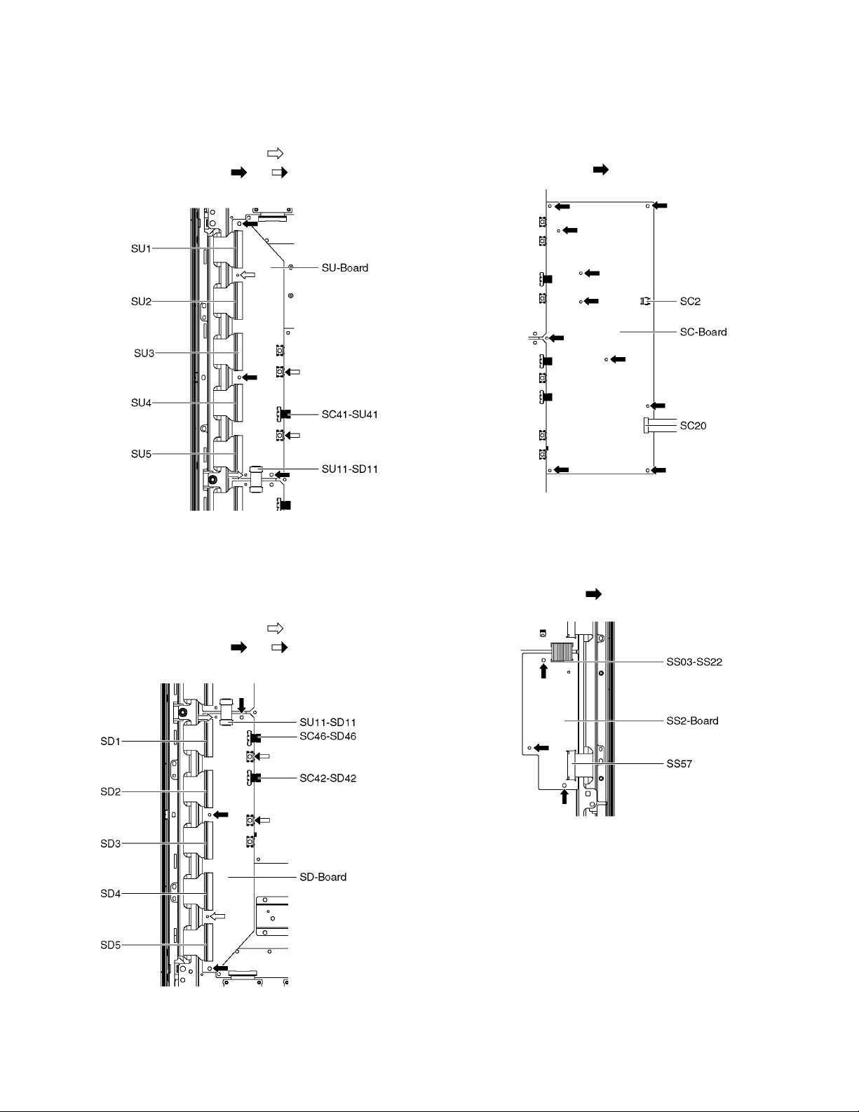
8.9. Remove the SU-Board
1. Remove the flexible cables (SU1, SU2, SU3, SU4 and
SU5) connected to the SU-Board.
2. Remove the flexible cable (SU11-SD11) and the bridge
connector (SC41-SU41).
3. Remove the molding props (×2 ).
4. Remove the screws (×3 , ×2 ) and remove the SU-
Board.
8.11. Remove the SC-Board
1. Remove the SU-Board and SD-Board. (See section 8.9.
and 8.10.)
2. Unlock the cable clampers to free the cable.
3. Disconnect the connector (SC2).
4. Disconnect the flexible cable (SC20).
5. Remove the screws (×10 ) and remove the SC-Board.
8.10. Remove the SD-Board
1. Remove the flexible cables (SD1, SD2, SD3, SD4 and
SD5) connected to the SD-Board.
2. Remove the flexible cable (SU11-SD11) and the bridge
connectors (SC42-SD42 and SC46-SD46).
3. Remove the molding props (×2 ).
4. Remove the screws (×3 , ×2 ) and remove the SD-
Board.
8.12. Remove the SS2-Board
1. Remove the Tuner unit. (See section 8.5.)
2. Disconnect the bridge connector (SS03-SS22) and disconnect the flexible cable (SS57).
3. Remove the screws (×3 ) and remove the SS2-Board.
24
Page 25
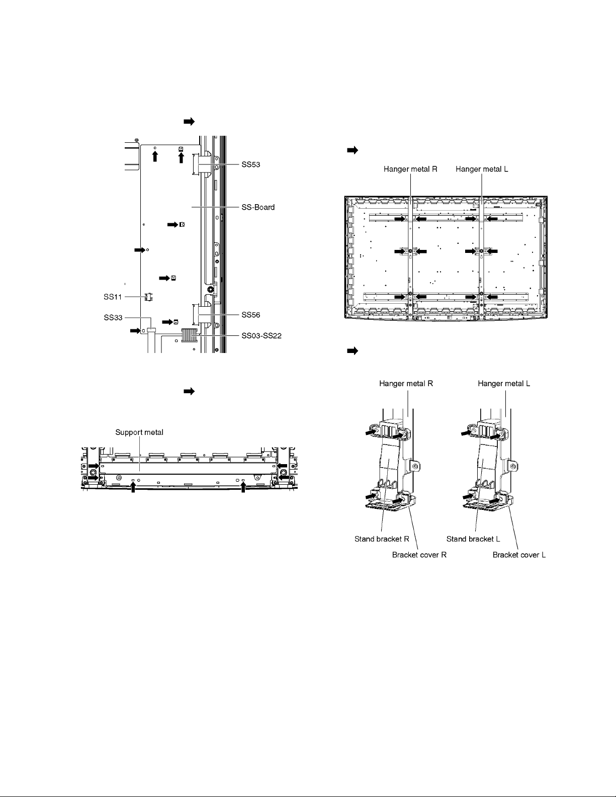
8.13. Remove the SS-Board
1. Remove the Tuner unit. (See section 8.5.)
2. Unlock the cable clampers to free the cable.
3. Disconnect the connector (SS11).
4. Disconnect the flexible cables (SS33, SS53 and SS56).
5. Disconnect the bridge connector (SS03-SS22).
6. Remove the screws (×7 ) and remove the SS-Board.
8.14. Remove the Support metal
1. Remove the screws (×6 ).
2. Remove the Support metal.
8.15. Remove the Hanger metals and the Stand brackets
1. Remove the Plasma panel section from the servicing
stand and lay on a flat surface such as a table (covered
by a soft cloth) with the Plasma panel surface facing
downward.
2. Remove the Support metal. (See section 8.14.)
3. Remove the Hanger metals (L, R) fastening screws (×6
each) and remove the Hanger metals (L, R).
4. Remove the Stand brackets (L, R) fastening screws (×4
each) and remove the Stand brackets (L, R) and the
Bracket covers (L, R).
25
Page 26
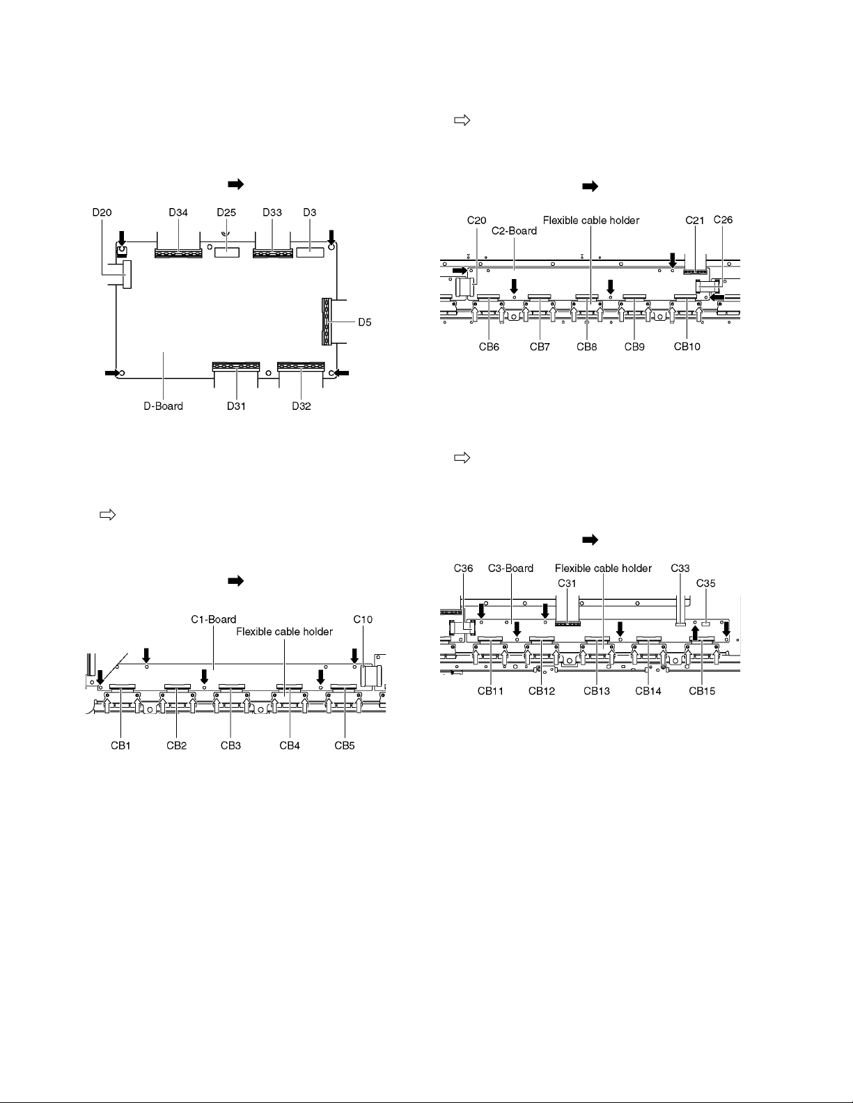
8.16. Remove the D-Board
1. Remove the Tuner unit. (See section 8.5.)
2. Remove the Hanger metal L and Stand bracket L. (See
section 8.15.)
3. Disconnect the flexible cables (D5, D20, D31, D32, D33
and D34).
4. Disconnect the connectors (D3 and D25).
5. Remove the screws (×4 ) and remove the D-Board.
8.17. Remove the C1-Board
1. Remove the Hanger metal R and Stand bracket R (See
section 8.15.).
2. Remove the flexible cable holder fastening screws (×10
).
3. Disconnect the flexible cables (CB1, CB2, CB3, CB4 and
CB5).
4. Disconnect the flexible cable (C10).
5. Remove the screws (×5 ) and remove the C1-Board.
8.18. Remove the C2-Board
1. Remove the Support metal. (See section 8.14.)
2. Remove the flexible cable holder fastening screws (×10
).
3. Disconnect the flexible cables (CB6, CB7, CB8, CB9 and
CB10).
4. Disconnect the flexible cables (C20, C21 and C26).
5. Remove the screws (×5 ) and remove the C2-Board.
8.19. Remove the C3-Board
1. Remove the Hanger metal L and the Stand bracket L.
(See section 8.15.)
2. Remove the flexible cable holder fastening screws (×10
).
3. Disconnect the flexible cables (CB11, CB12, CB13, CB14
and CB15).
4. Disconnect the flexible cables (C31, C33 and C36).
5. Disconnect the connector (C35).
6. Remove the screws (×6 ) and remove the C3-Board.
26
Page 27
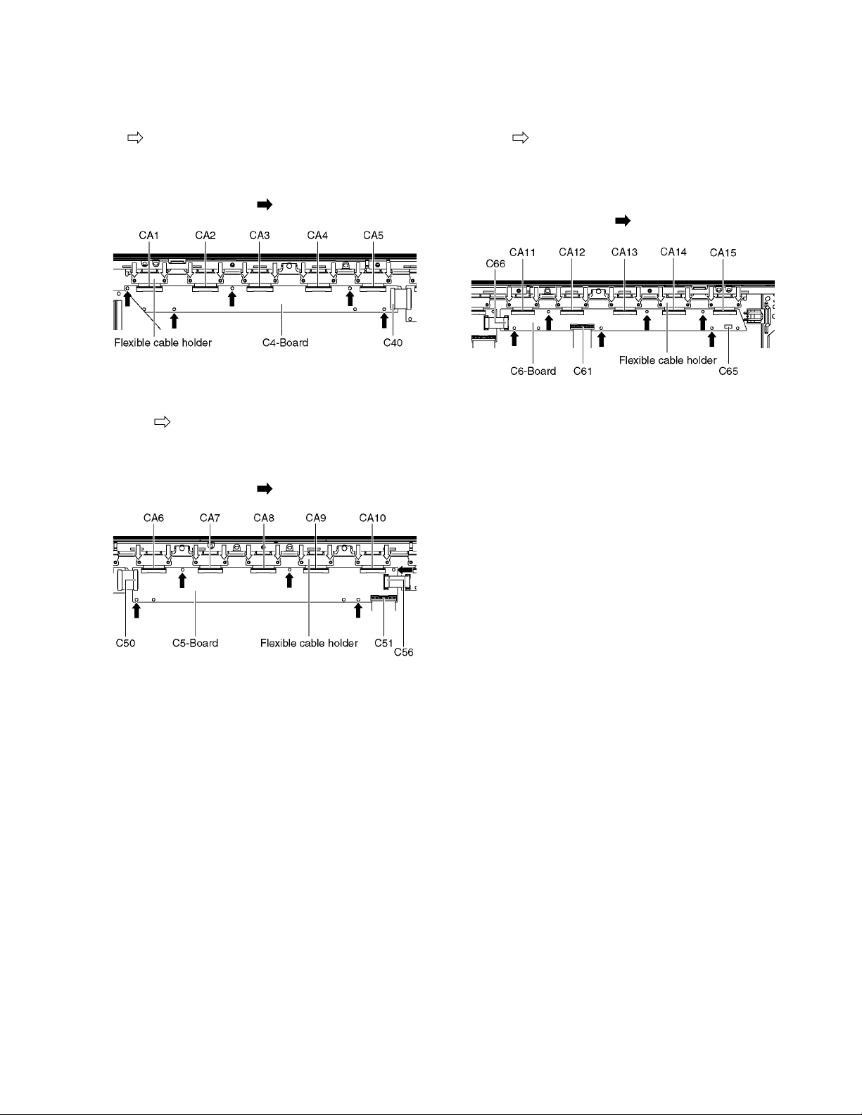
8.20. Remove the C4-Board
1. Remove the Hanger metal R and Stand bracket R. (See
section 8.15.)
2. Remove the flexible cable holder fastening screws (×10
).
3. Disconnect the flexible cables (CA1, CA2, CA3, CA4 and
CA5).
4. Disconnect the flexible cable (C40).
5. Remove the screws (×5 ) and remove the C4-Board.
8.21. Remove the C5-Board
1. Disconnect the flexible cable holder fastening screws
(×10 ).
2. Disconnect the flexible cables (CA6, CA7, CA8, CA9 and
CA10).
3. Disconnect the flexible cables (C50, C51 and C56).
4. Remove the screws (×5 ) and remove the C5-Board.
8.22. Remove the C6-Board
1. Remove the Hanger metal L and Stand bracket L. (See
section 8.15.)
2. Disconnect the flexible cable holder fastening screws
(×10 ).
3. Disconnect the flexible cables (CA11, CA12, CA13, CA14
and CA15).
4. Disconnect the flexible cables (C61 and C66).
5. Remove the connector (C65).
6. Remove the screws (×6 ) and remove the C6-Board.
27
Page 28
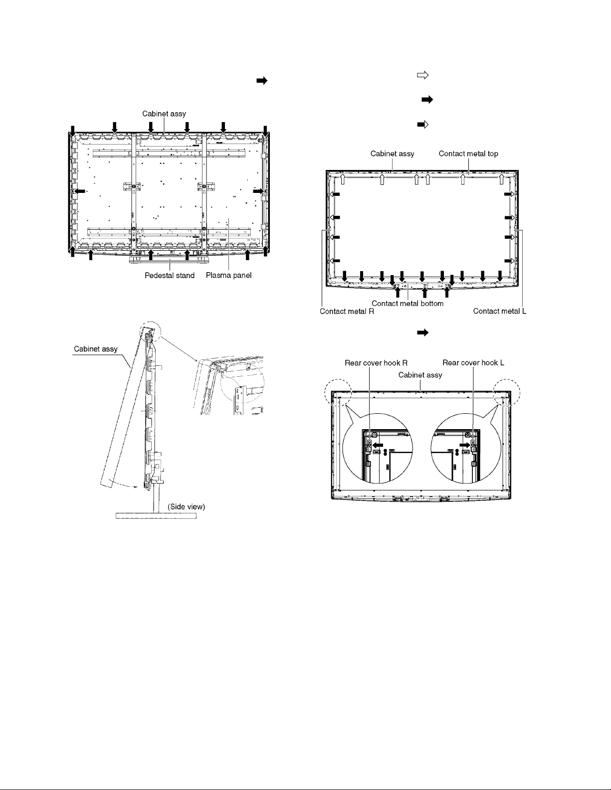
8.23. Remove the Plasma panel section from the Cabinet assy
1. Remove the plasma panel fastening screws (×14 ) and
remove the cabinet assy.
2. For leaving the cabinet assy from the plasma panel, pull
the bottom of the cabinet assy forward, lift, and remove.
8.24. Remove the Contact metals
1. Remove the Cabinet assy. (See section 8.23.)
2. Remove the screws (×6 ).
3. Remove the Contact metal top.
4. Remove the screws (×14 ).
5. Remove the Contact metal bottom.
6. Remove the screws (×8 ).
7. Remove the Contact metals (L, R).
8. Remove the screws (×2 ).
9. Remove the Rear cover hooks (L, R).
28
Page 29
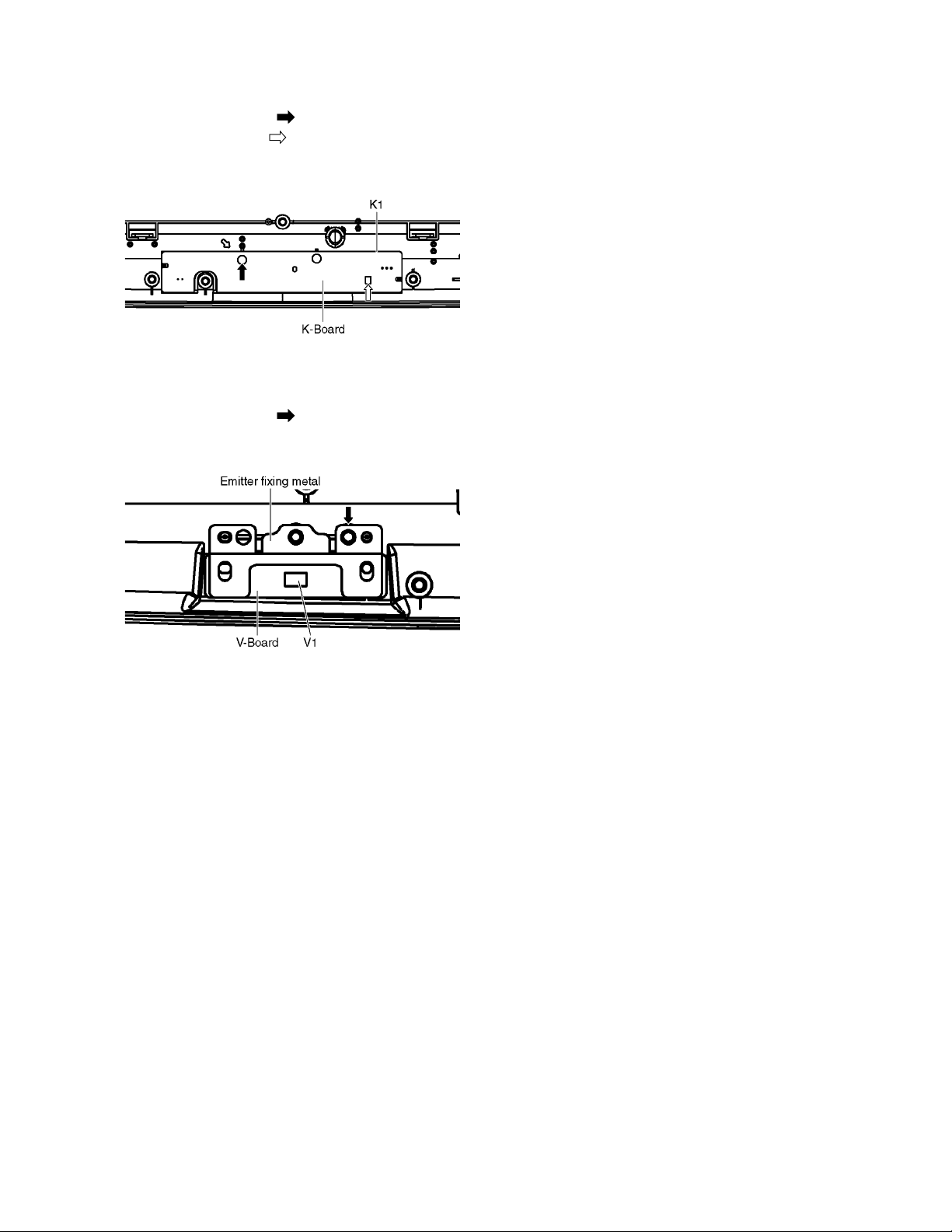
8.25. Remove the K-Board
1. Remove the Contact metal bottom. (See section 8.24.)
2. Remove the screw (×1 ).
3. Remove the claw (×1 ).
4. Disconnect the connector (K1) and Remove the K-Board
from LED Panel.
8.26. Remove the V-Board
1. Remove the Contact metal bottom. (See section 8.24.)
2. Remove the screw (×1 each).
3. Disconnect the connector (V1 each) and Remove the VBoard from the Emitter fixing metal.
8.27. Replace the plasma panel
Caution:
A new plasma panel itself without Hanger metals is
fragile.
To avoid the damage to new plasma panel, carry a new
plasma panel taking hold of the Hanger metals after
assembling the Hanger metals and the Stand brackets.
1. Place a carton box packed a new plasma panel on the flat
surface of the work bench.
2. Open a box and without taking a new plasma panel;
Attach the C1, C2, C3, C4, C5 and the C6-Board, connect
the flexible cables from the plasma panel to the C1, C2,
C3, C4, C5 and the C6-Board, and fit the flexible cable
holders.
3. Attach the Hanger metals and the Stand brackets to the
new plasma panel.
4. Place the plasma panel on the servicing stand taking hold
of the Hanger metals.
5. Attach the cabinet assy and each P.C.Board and so on, to
the new plasma panel.
29
Page 30
9 Measurements and Adjustments
9.1. Adjustment
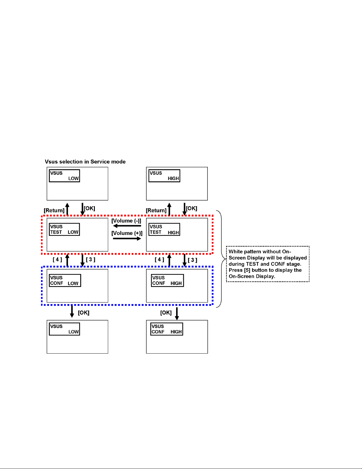
9.1.1. Vsus selection
Caution:
When Plasma panel or A-board is replaced, Vases should be set to LOW or HIGH.
Procedure
1. Go into main item [VSUS] in Service Mode. LOW or HIGH will be displayed.
2. Press [OK] button to go to TEST stage.
White pattern without On-Screen Display will be displayed during TEST and CONF stage. Press [5] button to display the
On-Screen Display.
3. Press [VOL (-)] button to set to LOW.
4. In LOW setting
a. If no several dead pixel is visible remarkably in white pattern, press [3] button to go to CONF stage.
b. If the several dead pixels are visible remarkably in white pattern, Set to HIGH by press [VOL (+)] button. Press [3] button
to go to CONF stage if the symptom is improved.
5. Press [OK] button in CONF stage to store LOW or HIGH.
6. Exit Service Mode by pressing [Power] button.
30
Page 31

9.1.2. RF video sub contrast adjustment
Name of measuring instrument Remarks
1. REMOTE TRANSMITTER
2. RF analog signal (Sprit color bar. The pattern for adjustment must contain 100% white part.)
Procedure Remarks
1. Receive the sprit color bar with RF analog signal.
(ASPECT FULL, Picture menu: Vivid)
2. Enter Service mode menu, and select ADJUST -- CONTRAST.
Pushing the remote controller [OK] key for about 3 seconds, GAIN is suited to the adjustment value automatically.
31
Page 32

9.1.3. White balance adjustment
Name of measuring instrument Remarks
Color analyzer
(Minolta CA-100 or equivalent)
Note:
The CA-100 which was calibrated to less than +-0.001 with CS-1000.
Procedure Remarks
• Make sure the front panel to be used on the final set is fitted.
• Make sure a color signal is not being shown before adjustment.
• Put the color analyzer where there is little color variation.
1. Set to Service mode, WB-ADJ.
2. Select [VIVID] for picture menu.
3. Select [Cool] for color temperature.
4. Push [5] key of remote controller to display window pattern.
5. Confirm the brightness. The following is the confirmation value.
TC-P58VT25 150cd/m2
6. Select [Cinema] for picture menu.
7. Select [Warm] for color temperature.
8. Set [R-CUT] [G-CUT] [B-CUT] the values written in table 1.
9. Attach the sensor of color analyzer to the center of window pattern.
10. Fix G drive at C0h and adjust [B-DR V] and [R -DRV] so x, y valu e of col or ana lyz er bec ome the [Co lor t emp era tur e
Low] in table 2.
11. Increase RGB together so the maximum drive value in RGB becomes [FF].
That is, set [ALL DRIVE] to [FF].
Execute adjustment again. When that, the maximum value of R/G/B DRV should be
[FF], and either R/G/B DRV should be [FF].
12. The average of the adjusted values in color temperature Cool, Mid, and Warm is shown in Table 4.
The setting value for color temperature Cool will be calc ula ted b y mu ltipl ying the adju sted val ue o f colo r tem per ature Warm to the ratio of the value of Warm and Cool in each GBR value in Table 4.
Write that values to the data area of color temperature Cool in EEPROM (Table 3).
13. The setting value for color temperatu re Mid will be ca lculated by multip lying the adjus ted value of color temperature Mid to the ratio of the value of Warm and Mid in each GBR value in Table 4.
Write that values to the data area of color temperature Mid in EEPROM.
14. Select [VIVID] for picture menu when you check the adjusted data of Cool and Normal.
Note:
Adjusted value
must be written to
both SD data area
and HD data area
of the EEPROM.
32
Page 33

33
Page 34

34
Page 35

(LED:6TIMES)
(LED:8TIME)
(LED:4TIME)
(LED:7TIMES)
(LED:4TIMES)
(LED:3TIMES)
(LED:6TIMES)
(LED:5TIMES)
(LED:9TIMES)
(LED:7TIMES)
(LED:8TIMES)
(LED:2TIMES)
HOT
COLD
HOTCOLD
Vda
DATA
DRIVER
DATA
DRIVER
C10 C20
P11
DATA
DRIVER
SC-BOARD
ENERGY RECOVERY
SOS DETECT
POWER MICOM
SC41
VIDEO DATA
DATA DRIVER (CENTER)
C3
RELAY
C31
STANDBY
VOLTAGE
RECTIFIER
P35
POWER
FACTOR
CONTROL
D32
SOS6_SC1
C35
C21
SUSTAIN CONTROL
SS2
SS-BOARD
SOS DETECT
SCAN DRIVE
SC46
SS33
BUFFER
SC20
DATA
DRIVER
SU11
STB5V
RECTIFIER
SS11
SC42
SC
VSUS GEN.
SUSTAIN CONTROL
C26
POWER SUPPLY
SU
Vda
SCAN
DRIVER
DATA DRIVER (LEFT)
VSUS
PS SOS4
ON/OFF CONTROL
DATA
DRIVER
SS22
MAIN SW2
SUSTAIN DRIVE
VIDEO DATA
SS
VE GEN.
DATA
DRIVER
SCAN CONTROL
ENERGY RECOVERY
VIDEO DATA
Vda
VSUS
VSCAN GEN.
CONTROL
PULSE
SOS8_SS
VAD GEN.
DATA
DRIVER
VSUS
C2
SCAN
DRIVER
CONNECTOR
P-BOARD
SOS DETECT
SD46
VSUS
SOS7_SC2
RECTIFIER
SCAN OUT (LOWER)
DATA
DRIVER
P34
SOS8_SS
C36
SC-BOARD
FLOATING PART
SOS DETECT
DATA
DRIVER
SD
SD42
DATA DRIVER (RIGHT)
P2
SUSTAIN CONTROL
C33
DATA
DRIVER
Vda
PROCESS
VOLTAGE
RECTIFIER
(LOWER)
MAIN SW1
SCAN OUT (UPPER)
SUSTAIN
VOLTAGE
RECTIFIER
SOS8_SS
SD11
Vda
AC CORD
SS03
SU41
P
SUSTAIN
DATA
DRIVER
F15V
DATA
DRIVER
P9
SC2
C1
VIDEO DATA
D31
P+15V
P+5V
P+5V
P+3.3V
P+3.3V
P+5V
P+15V
P+15V
P+3.3V,P+5V
P+3.3V
P6
D25
SOUND15V
STB5VSTB5V
F15V
P25
P+15V P+15V
P+5V
P+15V
C6DATA DRIVER (RIGHT)
C61
DATA
DRIVER
DATA
DRIVER
Vda
C65
DATA
DRIVER
Vda
C5
C51
DATA
DRIVER
DATA
DRIVER
DATA
DRIVER
C4
C56
P+3.3V
DATA DRIVER (LEFT)
P+3.3V
DATA
DRIVER
DATA
DRIVER
VIDEO DATA
Vda
DATA
DRIVER
DATA
DRIVER
C40 C50
DATA
DRIVER
DATA
DRIVER
C66
VIDEO DATA
DATA
DRIVER
DATA DRIVER (CENTER)
VIDEO DATA
P+3.3V
P65
Vda
A6
STB5V
P7A7
CONTROL
SIGNAL
POWER SOS
SCAN
CONTROL
SOS8_SS
EEPROM
P+15V
DCDC
SOS6_SC1
P+5V
SOS8_SS
P+3.3V
SOS_DCC
PANEL MAIN ON
PANEL MPU
SOS7_SC2
P+5V DET
SUSTAIN
CONTROL
P+5V
P+3.3V
P+3.3V
SOS6_SC1
SOS7_SC2
VIDEO DATA
P+15V
STB_D3.3V
P+3.3V DET
STB5V_M
STB_D3.3V
P+15V DET
PD4H
SLAVE PD4H
MASTER
VIDEO DATA
D33
D34
P+5V
PANEL READY
PANEL STB_ON
PANEL ALARM
D3
D20
A32
P+1.2V
P+5V
P+3.3V
DCDC
P+1.2V
P+5V
P+15V
DCDC
P+2.5V
P+2.5V
DCDC
P+3.3V
D5
LVDS DATA
A31
P+3.3VP+3.3V
VIDEO
DATA
P+3.3V
PD4HD
DATA
DRIVER
DATA
DRIVER
DATA
DRIVER
DATA
DRIVER
DATA
DRIVER
SUSTAIN
VOLTAGE
RECTIFIER
POWER
FACTOR
CONTROL
RELAY
P51 P52
MAIN
SUB
P56P55
P53 P54
RECTIFIER
(LED:6TIMES)
(LED:8TIME)
(LED:4TIME)
(LED:7TIMES)
(LED:4TIMES)
(LED:3TIMES)
(LED:6TIMES)
(LED:5TIMES)
(LED:9TIMES)
(LED:7TIMES)
(LED:8TIMES)
(LED:2TIMES)
HOT
COLD
HOTCOLD
(LED:10TIMES)
(LED:12TIMES)
(LED:12TIMES)
SOUND SOS
OPTICAL AUDIO OUT
ETHERNET DATA
SLOT
(SIDE)
Y/PB/PR
USB
USB
A11
REMOTE RECEIVER
L,R
KEYSCAN3
REMOTE IN
HDMI I/F
DRIVER
TRANSMITTER
LED(R)
V
SUB+5V DET
VIDEO1
OPTICAL
3D EYEWEAR
SUB5V
TUNER
3D EYEWEAR
TRANSMITTER
MIHO2_3.3V DET
R/G/B
AUDIO
A32
D3
COMP1
D5
PWMW
3D EYEWEAR
V
PWMS L/R
TRANSMITTER
ETHERPHY
REMOTE RECEIVER
A31
K1
USB_1,2
WOOFER
L/R MONITOR OUT
PC_H/V
L/R TV
SUB1.2V_A
SUB3.3V
SUB1.5V
L/R
SUB5V
Y/PR/PB
SIF_IN
3D EYEWEAR
A20
SIF_OUT
V1
V1
F15V
HDMI1-4
C.A.T.S. SENSOR
TMDS DATA
AMP1,2
PANEL ALARM
SUB1.5V
PANEL READY
SUB3.3V
OPTICAL OUT
STB3.3V
POWER SWITCH
SPEAKER(L,R)
STB3.3V
AV I/O
MPU
STB3.3V
STB5V
ASIC
ANALOG
SD CARD DATA
OUT
PEAKS-LDA2
SOUND SOS DET
CIRCUIT
AUDIO
LVDS DATA
PC
COMP2
SUB1.2V_A
DCDC
DCDC
SUB9V
A7
LVDS
DATA
PANEL STB_ON
ETHER_
NET IF
VIDEO2
10BASE-T/
SUB1.2V_V
ETHERNET
100BASE-TX
F15V
DCDC
MIHO-3D
WO
SUB1.2V_V
FRONT END
PROCESSOR
SD CARD
CH0DATA
A1
P6
SOUND15V
STB5V
L/R
DDR2
EEPROM
SUB+3.3V DET
TS_IN
SUB3.3V
AV SW
SOUND15V
V
KEY SWITCH
KEYSCAN1
POWER LED(R)
A
NAND
FLASH
L/R
CPU BUS
I/F
SUB9V
C.A.T.S. SENSOR
V
CPU BUS
SD CARD DATA
EEPROM
C.A.T.S. SENSOR
L/R
F15V
SUB9V
A6
ETHERPHY
P7
RECEIVER
POWER LED
DCDC
SUB5V
K
LED_8V DET
L/R
MIHO2_3.3V DET
Y/PB/PR
A12
LED_8V DET
IFD_OUT
DIGITAL SIGNAL PROCESSOR
(LED:10TIMES)
(LED:12TIMES)
(LED:12TIMES)
RS-232C
RS-232C
RS-232C
10 Block Diagram
10.1. Main Block Diagram
35
Page 36

10.2. Block (1/5) Diagram
DIGITAL SIGNAL PROCESSOR
A
V1_V
PC
STB5V
F15V
F15V
F15V
V1_L
V1_R
D1_Y
D1_PB
D1_PR
D1_L
D1_R
D2_Y
D2_PB
D2_PR
D2_L
D2_R
V2_V
V2_L
V2_R
PC_B
PC_G
PC_R
PC_H
PC_V
A7
P7
TV_SUB_ON
5
STB5V_SW_ON
8
1
A6P6
1
2
6
7
8
F15V
D5602
Q5603
F15V DET
JK3000
VIDEO1
COMP1
COMP2
JK3701
VIDEO2
(SIDE)
JK3001
TV_SUB_ON
STB5V_SW_ON
SOUND15V
SOUND15V
IC5401
9V
Q5602
ON/OFF
VIDEO1
V
L/R
VIDEO2
V
L/R
COMP1
Y/PB/PR
L/R
COMP2
Y/PB/PR
L/R
R/G/B
L/R
H/V
IIC0
PC
IC3001
AV SW
5V9V
STB5V
SUB9V
SOUND15V
IC5608
IC5501
TU8300
ANT IN
TV
V
L/R
MAIN
Y/PR/PB
L/R
H/V
MONITOR
IN
L/R LO1_L/R
3.3V
TV_V
VIDEO
TUNER
5V
SUB5V
TUNER
AFT
AFT
RF_AFT
SIF_OUT
IF_AGC
IC8303
IFD_OUT2
IFD_OUT1
SUB3.3V
1.2V
IIC_TU
IC4501
3.3V
DIGITAL
DEMODULATOR
VINP_VSB
IF_AGC
FRONT END
VINN_VSB
PROCESSOR
IC4500
HDMI
EQUALIZER
&SWITCH
IC8300
IIC_TU
IIC0
CH0DATA
SUB5V_USB
+5V
+3.3V
+1.5V
SUB3.3V
SUB1.5V
IC5607
5V
SUB5V
SUB3.3V
SUB1.5V
JK4503
HDMI IN 1
TMDS DATA
CLOCK
DDC IIC
+5V
ARC
HDMI_CEC
TS_IN
SIF_IN
Y/PR/PB
L/R
H/V
LO2_L/R
JK4500
HDMI IN 2
TMDS DATA
CLOCK
DDC IIC
SUB3.3V
+5V
HDMI_CEC
DDC IIC
RX1
RX0
HDMI I/F RECEIVER
AV I/O
CLOCK GEN
IC8240,41
JK4501
HDMI IN 3
TMDS DATA
CLOCK
RX2
IC8100
DDR3 #0
IC8501
NAND
FLASH
IC8502
EEPROM
DDC IIC
+5V
DDC_0_IIC
HDMI_CEC
DDC_2_IIC
DDC_1_IIC
JK4502
HDMI IN 4
(SIDE)
TMDS DATA
CLOCK
DDC IIC
CLOCK
IIC1
+5V
DDC IIC
DDR I/F
HDMI_CEC
HDMI5V_DET
HDMI_CEC
CPU BUS
I/F
IC8704
JK8700
USB_1,2
USB5V
SPEAKER_R
IC2301
Q2300
SOUND
SOS
DET
A11
AUDIO OUT
SPEAKER_L
12
L(+)
SPEAKER
D2303
SOUND
SOS
L(-)
L_OUT
SOS
PWMS L/R
PWMS L/R
3
R(+)
4
R(-)
R_OUT
SPEAKER
15V
PWMW
PWMW
LVDS_OUT
IC2302
AUDIO AMP2
SOUND15V
SUB3.3V
Q4537
OPTICAL
ARC_OFF
D3005
AUDIO
OUT
AUDIO AMP1
OPTICAL
AUDIO OUT
SPDIF
JK8702
10BASE-T/
100BASE-TX
ETHERNET
IC8703
ETHERNET IF
ETHER
NET
USB
ETHERPHY
USB
ETHERPHY
SD DATA:
4bit
SD CARD
JK8600
SD CARD
VDDSD
I/F
A12
15V
LVDS DATA
WOOFER
12
WO(+)
SOS
WO(-)
OUT
WOOFER
1
2
IC8000
PEAKS-LDA2
IIC0
IIC0
IIC1
IIC1
IIC2
IIC2
IC5603
3.3V
AVDDH
ACHIP3.3V
VCC
SUB3.3V
SUB1.5V
SUB1.2V_D
SUB1.2V_A
CLK
AX0
X8002
24.576MHz
POWER_DET
PA_NRST
AX1
SD BLUE LED ON
PD_XRST
IC5604
AVDDH
F15V
SD_BLUE_LED
IC5350
POWER_DET
DTV_XRST
RESET
F15V
STB5V
SUB9V
SUB5V
SUB3.3V
SUB5V_USB
3
4
5
6
7
8
9
IC5500
SUB1.2V_A
SUB1.2V_D
+1.2V
+1.2V
36
Page 37

(LED:12TIMES)
(LED:10TIMES)
S
SOS
SUB3.3V
D2520
SW2500
D5614
STB3.3V
D5615
D5613
SUB9V
SUB5V
SUB9V
STB5V
SUB3.3V
STB3.3V
D5470
Q5478
Q5475
SUB5V
D2500 D2502
D2501
LED_7V_1
LED_7V_2
F15V
F15V
X5800
27MHz
X1100
Q5684
D2500 D2502
D2501
D2659
D2660
D5519
D5522
Q5522
Q5479
D5524
SUB5V_USB
STB3.3V
LED_8V
LED_8V
D2521
TEMP SENSOR
IC4800
IIC0
TV SUB ON
TV SUB ON
SUB3.3V DET
SUB5V DET
STB+3.3V
1
RM2501
C.A.T.S.
1
C.A.T.S.
SENSOR
C.A.T.S.
REMOTE IN
STB3.3V
A1
FOR
FACTORY
USE
K
REMOTE
RECEIVER
REMOTE RECEIVER
POWER LED
C.A.T.S. SENSOR
POWER LED
3
6
5
POWER LED(R)
5
2
R_LED_ON
6
A17
A18
FOR
FACTORY
USE
2
SUB3.3V
REMOTE IN
3
SN2510
K1
KEYSCAN3
POWER SWITCH
KEYSCAN1
GENX
IIC
GENX
IIC
EEPROM
IC1101
STB_RST
RESET
IC5606
STB_RST
KEYSCAN3
IC5480
ANALOG-ASIC
MPU
GenX8
STB3.3V
STB_RST
STB_RST
DTV_XRST
DTV_XRST
IIC1
IIC1
6
7
3
8
5
2
LVDS DATA
IC1100
IIC2
AVC
IIC0
STB5V_SW_ON
POWER_DET
SW_OFF_DET
SW_OFF_DET
STB_RST
A
DIGITAL SIGNAL PROCESSOR
IR_L
4
1
LED_7V
V1
IIC_CLK1
IIC_CLK2
3
IIC_DATA1
PANEL STB_ON
2
PANEL
IIC2
8
IIC_DATA2
READY
PANEL READY
D3
10
7
A32
PANEL ALARM
PANEL STB_ON
AVC_
IIC0
ALARM
11
4
MIHO2_3.3V
IC5811
+3.3V
MIHO2_1.2V
IC5806
+1.2V
LED_8V
IC5808
+8V
IC5809
7V
7V
IC5810
NAND
FLASH
CPU BUS
I/F
IC5801
XTALIN
XTALOUT
MIHO2_3.3V
MIHO2_1.2V
LVDS DATA
LVDS DATA(LEFT)
LVDS DATA(RIGHT)
MIHO-3D
IC5800
PANEL STB_ON
PANEL READY
PANEL ALARM
PANEL STB_ON
PANEL READY
PANEL ALARM
PANEL STB_ON
2
36
A31 D5
67
33
LVDS DATA(LEFT)
LVDS DATA(RIGHT)
DDC_1_IIC
DDC_2_IIC
HDMI_CEC_IN_OUT
SOUND SOS
DDC_2_IIC
DDC_0_IIC
DDC_1_IIC
DDC_0_IIC
HDMI_CEC_
IN_OUT
SOUND SOS
RF_AFT
RF_AFT
HDMI5V_DET2
HDMI5V_DET1
HDMI5V_DET0
HDMI5V_DET2
HDMI5V_DET1
HDMI5V_DET0
KEY SWITCH
VOL.UP
VOL.DN
CH.UP
CH.DN
INPUT/OK
MENU
SW3764
SW3765
SW3759
SW3761
SW3762
SW3763
10MHz
X0
XI
KEYSCAN1
KEYSCAN3
KEY3/STBY_LED_ON
KEYSCAN1
REMOTE IN
POWER LED(R)
C.A.T.S.
POWER LED(R)
REMOTE IN
C.A.T.S. SENSOR
IIC2
IIC2
IC5805
1.2V
PLL_1.2V
4
1
A20
A+IN
B+IN
V+
IR_L
4
1
LED_7V
V1
8
5
A-OUT
B-OUT
IC5813
5V
IR_L
SW OFF DET
SW OFF DET
SOS
SOS
MIHO2_3.3V DET
LED_8V DET
IR
DRIVE A
IR
DRIVE B
Q5814
Q5813
TRANSMITTER
V
3D EYEWEAR
DRIVER
3D EYEWEAR
TRANSMITTER
V
3D EYEWEAR
IC5814
4
9
1
SD_BLUE_LED
88
SD_BLUE_LED
SD_BLUE_LED
GENX
IIC
IIC0
IIC2
PANEL_IIC2
GENX_IIC
IIC1
PANEL_IIC2
TRANSMITTER
3D EYEWEAR
3D EYEWEAR
TRANSMITTER
(LED:12TIMES)
(LED:10TIMES)
SBO1
TXD
SBO1
IC3002
RS232C
RS232C SBI1
DRIVER
RS-232C
SBI1
RS232C SBO1
RS-232C
RS-232C
JK3003
RXD
SBI1
10.3. Block (2/5) Diagram
37
Page 38

10.4. Block (3/5) Diagram
(LED:4TIMES)
HOT
HOT COLD
COLD
HOT COLD
SUB
P
POWER SUPPLY
F801
10A 250V
RF801
HOT
COLD
K802
RUSH RELAY1_ON
MAIN
PC903
PHOTO COUPLER
PC902
PHOTO COUPLER
PC801
PHOTO COUPLER
D251
+-
D401
RECTIFIER
D351
K805
K804
T901
D953
Vsus
ERROR
DET
D402
L401
Vsus
VR251
IC251
Vsus
ERROR
DET
BIAS_PFC
BIAS_MAIN
SUS_Vo1
D701
10A 250V
F802
RECTIFIER
D803
Q808
OVP
2A 250V
F501
D501
PFC ON
VDET
IS
Q809
L803
VDET
IS
Vcc
Q601,Q604,Q606
CONTROL
IC601
Q602,Q603
PFC/DRIVER
Q503
Q504
ZD603
IC501
STB
CONTROL
Q804, Q806
CONTROL
IC801
Q802,Q803
PFC/DRIVER
FB
Vcc
OVP DET
D
S
5A 250V
Q507
D508
OVP
C
Q508
FB
F201
Q203
BIAS2(+)
BIAS1(+)
Q903
Vsen
Vc1
Q204
5A 250V
F901
Vsus
ON
Q904
Q201,Q202
RESONANCE
IC201
MULTI
POWER
CONTROL
IC202
BIAS1_MAIN
BIAS1_PFC
D510
D504
PHOTO COUPLER
D505
+
-
VGLVGH
T501
Vsen
Vc1
OCP
FB
PC510
PC502
Q901,Q902
RESONANCE
IC901
Vsus
POWER
CONTROL
IC902
+
-
D552
D551
STB+DET
VGLVGH
OCP
FB
HOT COLD
T201
PC201
PHOTO COUPLER
PC202
PHOTO COUPLER
PC501
PHOTO COUPLER
STB-IN
DET
ZD552
D554
STB+5V DET
D555
RECTIFIER
ZD553
L801
BIAS1(+)
Q805
Q807
OVP
ZD803
G
1
2
2
1
RECTIFIER
BIAS(-) BIAS(-)
D603
L603
BIAS1(+)
4
4
P53
P54
NEUTRAL NEUTRAL
BIAS(+)
BIAS(+)
LIVE
1
P51
1
P52
LIVE
Q607
Q605
G
RECTIFIER
PHOTO COUPLER
Q709
RUSH
RELAY
ON
IC551
F_STB
ERROR
DET
Q711
MAIN
RELAY
ON
AC DET
D708
D707
Q702
NEUTRAL
LIVE
L601
L602
F601
10A 250V
LIVE
NEUTRAL
LIVE
LINE
FILTER
F602
10A 250V
NEUTRAL
LIVE
1
2
P9
ZD505
AC DET
ZD503
Q505
Q502
RF601
Q506
K605
K604
K602
PC504
PHOTO COUPLER
HOT COLD
MAIN RELAY ON
VDD
MAIN RELAY1_ON
IC951
Vsus_ON
BIAS_PFC_ON
Q404
OCP
ZD401
ZD351
Q356
Q251,Q252
V_SET
CONTROL
POWER MICOM
FV ON
AC DET
P34
STB_IN
Q357
OVP
MC701
STB_IN
MAIN SW_ON
3
1
Vsus
VR951
OVP
DET
Q405,Q406
D706
Q561
Q951
V_SET_1
Q952
V_SET_2
IC403
V_SET1
V_SET2
POWER SOS
(LED:4TIMES)
STB+5V
MC551
Q560
Vda
CONTROL
Q407,Q408
SUS_Vo2
Vda_Vo
SUS_S0
SUS_S1
PANEL_ON
ALL_OFF
FSTB_ON
+15(DD)Vo
STB_ON
+5V
D556
FET
DRIVER
BIAS_MAIN
BIAS_PFC
Q559
D557
15V
9
P55
9
P56
D403
Q401
CONT
D705
MAIN RELAY1 ON
RUSH RELAY1_ON
Q558
STB_IN
Q706
Q551
FSTB+15V
QN
7
7
Q712
V_SET_2
V_SET_1
610 2 158
5
610 2 18
Q710
SUS_Vo2
4
34
3
RUSH RELAY1
MAIN RELAY1
+15V_ON
IC352
Q557
STB+5V ON
P2
Vsus
Vda
Q402
Vda
DET
Q403
Vda
VR401
L402
Q355
L351
PGATE
ILIM
VIN
FB
EN
+15V
CONTROL
SC2
1
Vsus
SS11
P11
1
Vsus
15V
4
+15V(P)
C35
P35
1
Vda
2
Vda
C65
P65
1
Vda
2
Vda
D25
P25
1
+15V(P)
2
+15V(P)
5
STB+5V
7
S0
8
S1
9
PANEL_MAIN_ON
10
SOS4_PS
A7
P7
1
STB+5V
3
S0
4
S1
5
F_STB_ON
7
PANEL_MAIN_ON
8
STB5V_ON
9
SOS4_PS
11
ALL OFF
12
MAIN SW1
14
MAIN SW2
P6
A6
1
SOUND+15V
2
SOUND+15V
P+15V
3
7
FSTB+15V
9
FSTB+15V
AC CORD
38
Page 39

10.5. Block (4/5) Diagram
(LED:2TIMES)
(LED:3TIMES)
(LED:5TIMES)
(LED:8TIMES)
(LED:9TIMES)
(LED:7TIMES)
(LED:4TIMES)
(LED:6TIMES)
P+5V
P+5V
P+3.3V
P+15V
P+3.3V
P+5V
X9400
P+1.2V
STB_D3.3V
P+2.5V
P+5V
P+3.3V
X9000
P+15V
P+3.3V
P+3.3V
P+15V
STB5V
P+15V
P+15V
P+3.3V
P+3.3V
P+15V
P+3.3V
P+3.3V
P+3.3V
DCC_SOS
BUFFER
P3V_
IIC2
P+3.3V
44
STB
IIC2
1.2V
SUSTAIN CONTROL
IC9001
C40
C51
PANEL DRIVER
15
CA4
P3V_
IIC2
IC9401-03
VIDEO DATA
BUFFER
P+3.3V DET
P+5V
1
VIDEO DATA
P3V_
IIC1
EEPROM
PANEL MPU
DATA DRIVER (CENTER)
STB_D3.3V
52
PD4H SLAVE
C65
DISCHARGE CONTROL
55
3.3V
CA3
2
47
UHZ
IC9400
P+15V
SOS4_PS
RESET
D25
SCAN CONTROL
VIDEO DATA
1.2V
VIDEO DATA
P3V_
IIC2
DATA DRIVER (RIGHT)
66
D31
IC9810,11
BUFFER
PANEL READY
(STATUS)
P_S0
Vda
BUFFER
XRSTSYS
CONTROL DATA
PLASMA PANEL
XRSTSYS
CA8 CA9
SOS7_SC2
STB_IIC2
8
29
66
SCAN
CONTROL
DRVRST
P+15V
STB_
IIC1
P_S0
D32
IC9802
P3V_
IIC2
P25
C4
IIC_CLK1
XO
P_S0
STB5V
CA7
2
XI
READY
XI
67
XO
236
POWER ON/OFF
16
SOS6_SC1
D34
50
D20
653
XRSTSYS
27
63
9
16
PANEL STB_ON
6
P3V
IIC1
1
SOS4_PS
IIC_DATA1
PANEL_MAIN_ON
PANEL ALARM
P_S1
XRSTSYS
P+3.3V
1
DRVRST
CONTROL DATA
66
47
P+15V
PANEL STB_ON
8 68
ALARM
41
PLASMA AI
CPG with SS
H/V Sync Control
Sub Filed Processor
3
P65
48
P+3.3V
OSD I/F
SC20
15
+2.5V
SOS7_SC2
6863
IIC2
PD4H MASTER
42
9
RESET
C5
30
SOS6_SC1
4
SOS8_SS
SOS4_PS
59
18
SOS6_SC1
6
5
1
OSD I/F
VIDEO DATA
10
GenX7
3
SOS6_SC1
FLASH
MEMORY
P_S1
IIC_CLK2
SOS7_SC2
D5
P_S0
STB
IIC2
19
IIC_DATA2
33
SOS8_SS
LVDS DATA1
(RIGHT)
IC9304
LVDS DATA2
(RIGHT)
SOS8_SS
LVDS DATA1
(LEFT)
SOS7_SC2
9
30
XRSTSYS
XRSTSYS
PANEL ALARM(SOS)
CA
10
DRVRST
PANEL MAIN ON
PANEL READY
IC9004
OSD I/F
+3.3V
CA
11
PANEL STB_ON
IC9801
Vda
SOS4_PS
DRVRST
PANEL_MAIN_ON
2.5V
CONTROL DATA
STB+3.3V/RESET
P_S1
63
PLASMA AI
CPG with SS
H/V Sync Control
Sub Filed Processor
Vda
44
FLASH I/F
VIDEO DATA
LVDS DATA2
(LEFT)
10
ADDR/DATA
LVDS DATA1
(RIGHT)
12
P+5V DET
LVDS DATA2
(RIGHT)
50
55
LVDS DATA1
(LEFT)
IC17601
LVDS DATA2
(LEFT)
5
DC/DC OE
CA1
IC9003
PANEL MAIN ON DCC_SOS
IIC1
DCC_SOS
DCC_SOS
OSD I/F
1
DCC_SOS
P+15V DET
68
CONTROL DATA
1
D33
C6
CA
14
P+3.3V
1
PANEL DRIVER
Vda
3.3V
CONTROL DATA
CA
12
UHZ
16
IC9300
STB_
IIC2
+5V
STB_
IIC1
2.5V
CONTROL DATA
CA2
C66
25
+1.2V
PANEL DRIVER
+3.3V
CA
13
26
VIDEO DATA
VIDEO DATA
42
VIDEO DATA
C56
P+15V
A31
19
47
TEMP SENSOR
C50
Vda
VIDEO DATA
IC9002
7
P+3.3V
FOR
FACTORY
USE
Vda
P_S1
D6
25
10
DC/DC OE
IC9804
P3V_IIC1
A32
DATA DRIVER (LEFT)
PANEL READY
D3
C61
CA
15
10211
PANEL ALARM
P+3.3V
DCC_SOS
IC17501
CA5 CA6
31416
53 42 40
VIDEO DATA
28
274
3
515
VIDEO DATA
P+3.3V
47
CONTROL DATA
PANEL DRIVER
C33
Vda
30
15
9
C20
CB2
C2
C35
IC17301
28
P+3.3V
41
1
50
1
P+5V
SUSTAIN
CONTROL
6
VIDEO DATA
CB
15
DATA DRIVER (CENTER)
19
BUFFER
CB7
CB
13
C3
3
6
CB4
IC17302
5
20
SOS8_SS
PANEL DRIVER
Vda
52
CB3
4
SS33
51
VIDEO DATA
SUSTAIN CONTROL
1
P+3.3V
3
6
12
1
P+5V
P+3.3V
P+3.3V
PLASMA PANEL
19
C31
CB
12
P+5V
C21
DATA DRIVER (LEFT)
55
5
CB9
27
BUFFER
Vda
P+3.3V
PANEL DRIVER
26
P+3.3V
59
Vda
P+3.3V
C26
1
25
2
55 53
BUFFER
27
VIDEO DATA
25
C36
CB
14
Vda
6
CB5 CB6
Vda
CB1
IC17201
1
CB
10
DATA DRIVER (RIGHT)
3
SOS8_SS
21
CB
11
C10
66
P35
VIDEO DATA
4
CB8
C1
314
(LED:2TIMES)
(LED:3TIMES)
(LED:5TIMES)
(LED:8TIMES)
(LED:9TIMES)
(LED:7TIMES)
(LED:4TIMES)
(LED:6TIMES)
PD4H
D
39
Page 40

10.6. Block (5/5) Diagram
(LED:6TIMES)
(LED:8TIMES)
(LED:7TIMES)
SC
SCAN DRIVE
TPVSUS
P2
SC2
1
SOS6_SC1
SOS7_SC2
SCAN CONTROL
D20
P+15V
P+15V
P+5V
Vsus
SC
20
35
18
UHZ
21
20
IC16771
Vad+5V
CSL
CML
PC16461
PHOTO
COUPLER
Q16501,02.31
IC16501
CSH/CMH GATE
DRIVE CIRCUIT
Q16521,22,51
IC16521
CSL/CML GATE
DRIVE CIRCUIT
CMH
CSH
IC16581
ERROR DET
7
6
TPSOS6
(LED:6TIMES)
(LED:7TIMES)
INVERTER
UHZ
D16822
TPSOS7
CMH
CSH
CSL
CML
IC16563
SCAN CONTROL
SCAN CONTROL
D16493
SOS6_SC1
D16820
D16480
CERS
CPH1
CIS
Q16403
D16463,64
Q16441,42
D16583
LED(G)
D16920
Q16876
ERROR DET
PC16480
PHOTO
COUPLER
F16V
PC16603
PHOTO COUPLER
PC16684
PHOTO COUPLER
PC16685
PHOTO COUPLER
-06
VRH
MID
Q16421-24
CRC1
WAVEFORMSHAPER
WAVEFORMSHAPER
CRC2
IC16561,62
BUFFER
IC16564
AND
Q16920
IC16490,91
SEPA PROTECT
CIRCUIT
Q16621-23
L16401
VRL
D16481,82
Q16670,71
Q16675,76
D16821
IC16471
SHUNT
REG
Q16607
CIS
L16411
Q16453,54
CML
CMH
CSH
CSL
SEL2
Q16490
D16618
Q16601
CPH1
CIS
CERS
CEL
VOL
D16490
D16871
Q16471
SIU
OC1
OC2
CLK
SEL
CRC1
CRC2
VFG
D16475
D16859
64
Q16818
TPVAD
Q16647
Q16668
D16652
Q16660
TPSC1
TP59,TP60
TP61,TP62
5V_F
CHA
Q16661
VSCN-F
Vsus
IC16661
COMPARATOR
IC16920
COMPARATOR
IC16784,85
PC16896
IPD CIRCUIT
VAD GEN.
SHUNT REG
Q16885
F16V
F16V GEN.
IC16773
CEL
INVERTER
CEL
IPD CIRCUIT
VSCN GEN.
SHUNT REG
IC16786,87
(16V_F)
PC16722,23
D16721
15V_F
Vscn
D16473
+5V
IC16724
SCNR_PRO
CRC1
CRC2
T16471
D16728
IC16691
TPVSCN
D16901
Q16662,63
IC16692
NAND
VFG
D16662
Q16608
SHUNT
REG.
SC
50
VFG
1
SC JIG
2
SU
SCAN OUT (UPPER)
IC14901,02
SCAN
DRIVER
9
8
4
2
SU1-SU5
PLASMA PANEL
PANEL SCAN
ELECTRODE
SD1-SD5
IC14904,05
SCAN
DRIVER
SCAN
DRIVER
IC14907,08
SU
11
SD
11
CHA
SC
SU
41
VFG
Vfo
41
9
8
2
IC14951,52
SCAN
SEL2
DRIVER
SD
42
5
6
2
1
8
9
SD
46
IC14961,62,64
SCAN OUT (LOWER)
SD
IC14954,55
DRIVER
DRIVER
IC14957,58
SCNR_PRO
CHA
LOGIC IC
SCAN
SCAN
SC
42
5
6
2
Vfo
1
8
9
SC
SIU
46
OC1
OC2
CLK
SEL
SOS8_SS
SUSTAIN CONTROL
P11
P+15V
Vsus
C33
P+5V
P+5V
SS
SS
11
1
4
SS
33
1
2
20
SUSTAIN CONTROL
SUSTAIN DRIVE
Q16141,61
IC16131
VSUS Gen.
DRIVER
Q16055,56
IC16151
ENERGY
RECOVERY
IC16241
BUFFER
TPVSUS
UMH
UML
USH
USL
UEH
UML
UMH
TPSOS8
(LED:8TIMES)
Q16002-04
Q16022-24
D16042,43
Q16041,42
Q16051,52
Q16251
IC16251
ERROR DET
USL
USH
D16255
D16051,52
D16253
LED(G)
FPC DET
D16316
VE GEN.
PHOTO
COUPLER
Q16191
PC16191
VE Gen.
DRIVER
D16280
IPD CIRCUIT
IC16304
PC16301
IC16312
L16303
SHUNT
REG.
UEH
UML
Q16280
ERROR DET
Q16101.02
TPSS1
TPVE
D16282
SS
53
1
2
13
PLASMA PANEL
PANEL SUSTAIN
ELECTRODE
SS
56
1
2
13
SS
13
1
2
57
SS
SS
22
03
343
4
4
23
23
SS2
SUSTAIN
CONNECTOR
(LOWER)
40
Page 41

11 Wiring Connection Diagram
11.1. Caution statement.
Caution:
Please confirm that all flexible cables are assembled correctly.
Also make sure that they are locked in the connectors.
Verify by giving the flexible cables a very slight pull.
11.2. Wiring (1)
11.3. Wiring (2)
41
Page 42

11.4. Wiring (3)
42
Page 43

11.5. Wiring (4)
43
Page 44

11.6. Wiring (5)
44
Page 45

11.7. Wiring (6)
45
Page 46

11.8. Wiring (7)
46
Page 47

12 Schematic Diagram
12.1. Schematic Diagram Note
47
Page 48

12.2. P(MAIN)-Board (1/3) Schematic Diagram
TO
P(SUB)-BOARD
(P51)
COLD
HOT
A
B
PFC
C
TO
P(SUB)-BOARD
(P53)
HOT
COLD
D
F_STB ERROR DET
STB CONTROL
E
+5V
F
P(MAIN)-BOARD ETX2MM812MDM (1/3)
!
HOT
2 896
4
5
COLD
731
48
Page 49

12.3. P(MAIN)-Board (2/3) Schematic Diagram
E
B
4
D
731
C
5
F
2 896
A
MULTI POWER
CONTROL
COMPARATOR
COLD
HOT
Vsus
ERROR DET
Vsus
Vda
CONTROL
Vda
COLD
HOT
!
P(MAIN)-BOARD ETX2MM812MDM (2/3)
+15V CONTROL
TO
SS-BOARD
(SS11)
TO
C3-BOARD
(C35)
TO
C6-BOARD
(C65)
TO
A-BOARD
(A6)
49
Page 50

12.4. P(MAIN)-Board (3/3) Schematic Diagram
A
B
C
TO
D-BOARD
(D25)
TO
A-BOARD
(A7)
D
E
POWER MICOM
P(MAIN)-BOARD ETX2MM812MDM (3/3)
F
TO
P(SUB)-BOARD
(P55)
2 896
4
5
!
731
50
Page 51

12.5. P(SUB)-Board Schematic Diagram
COLD
HOT
COLD
HOT
E
B
4
D
731
C
5
F
2 896
A
TO
P(MAIN)-BOARD
(P52)
TO
P(MAIN)-BOARD
(P54)
PFC
Vsus POWER
CONTROL
COMPARATOR
Vsus
ERROR DET
Vsus
TO
SC-BOARD
(SC2)
!
P(SUB)-BOARD ETX2MM812MDS
TO
P(MAIN)-BOARD
(P56)
51
Page 52

12.6. A-Board (1/20) Schematic Diagram
!
LDA2_ROM,SPCA-BOARD TXN/A1LZUUS (1/20)
A
B
C
PEAKS-LDA2
TO 17/20
TO 17/20
TO 2,17/20
TO 17/20
PD_ED[0-15]
PD_NFRYBY
PD_XNFRE
PD_XNFCE
PD_NFCLE
PD_NFALE
PD_XNFWE
PD_XNFWP
PD_ED0
PD_ED1
PD_ED2
PD_ED3
PD_ED4
PD_ED5
PD_ED6
PD_ED7
R8918
EXB2HV680JV
R8944
R8945
R8946
R8947
R8948
R8949
AH_ED0
AH_ED1
AH_ED2
AH_ED3
AH_ED4
AH_ED5
AH_ED6
AH_ED7
56
56
56
56
56
56
AH_ED6
AH_ED4
AH_ED7
AH_ED5
45NC46NC47NC48
NC
1NC2NC3NC4NC5NC6NC7
I/O442I/O543I/O644I/O7
IC8501
TVRR440ADS
R/B#8RE#9CE#10NC11NC12VCC13VSS14NC15NC16CLE17ALE18WE#19WP#20NC21NC22NC23NC24NC
R8950
56
R8951
2.2k
C8903
16V
0.1u
37
38NC39NC40NC41
VSS
VCC
1Gbit NAND_FLASH
C8904
16V
0.1u
AH_ED2
AH_ED1
AH_ED0
AH_ED3
SUB3.3V
DEBUG CONNECTOR
33NC34NC35NC36
25NC26NC27NC28NC29
I/O030I/O131I/O232I/O3
SUB3.3V
R8973
R8952
10k
10k
R8972
10k
SUB3.3V
R8963
10k
R9014
10k
PEAKS-LDA2
PD_XIRQ1
TO 17/20
TO 17/20
JTAG
R8965
10k
R8975
10k
PD_TCK
PD_TDI
PD_TMS
PD_TRST
PD_EVTRG
D
EEPROM
*IC8502
TVRR680S
E
1
2
3
4
EEPROM
NC
NC
NC
VSS
SUB3.3V
C8950
16V
TP8563
0.01u
8
R8500
VCC
4.7k
7
WC
R8503
S
6
SCL
S
5
SDA
R8504
R8501
TO 17/20
68
PD_HSDOUT6
PORT5[7]EEPROM_WP
TO 2,8,12/20
IIC1
PEAKS_SCL1
PEAKS_SDA1
F
743
91 6825
52
Page 53

12.7. A-Board (2/20) Schematic Diagram
CLK Gen
!
X8100
H0J270500120
27MHz
C8151
C8150
50V
50V
0.5p
IC8100
C1ZBZ0003967
CLOCK GEN
12p
1
X1
2
S0
3
S1
4
VIN
5
VDD1
C8155
16V
6
0.01u
GND1
7
CLK1
8
CLK2
R8102
56
R8103
56
REFOUT
X2
VDD3
S2
VDD2
GND2
CLK4
CLK3
IIC
SUB3.3V
10k
10k
10k
R8546
R8545
R8544
10k
10k
10k
10k
10k
10k
10k
10k
R8556
R8552
R8550
R8551
R8549
R8553
R8554
R8555
IIC_BUS
PEAKS-LDA2 I2CBUS
TO 17/20
PD_SCL0
PD_SDA0
PD_SCL1
PD_SDA1
PD_SCL2
PD_SDA2 PEAKS_SDA2
R8680
R8681
R8682
R8683
R8684
R8685
SUB3.3V
L8100
J0JHC0000045
R8104
16
C8152
10k
0.1u
16V
15
14
13
12
11
10
9
10k
R8557
S
S
S
S
S
S
R8105
56
C8153
0.1u
16V
C8154
10u
10V
R8108
56
R8111
56
ETHER_25M
TP8100
C8157
10V
1u
10k
10k
10k
10k
R8562
R8558
R8559
R8560
boot_mode_sel[0]
boot_mode_sel[1]
boot_mode_sel[2]
boot_mode_sel[3]
boot_mode_sel[4]
clk_mode[0]
clk_mode[1]
clk_mode[2]
clk_mode[3]
clk_mode[4]
clk_mode[5]
use_PCI_raw
pci_host_sel_raw
ed_pullup_sel
ea_pullup_sel
BOOTBT
eclk_mode[1]
eclk_mode[0]
pcitest_sg
cputest_sg
SDBOOT
rom_boot_size[0]
rom_boot_size[1]
mode_sel_soft
10k
10k
10k
1k
10k
1k
R8565
R8566
R8564
R8587
R8572
R8585
SUB3.3VMIHO2_3.3V
2.7k
2.7k
2.7k
2.7k
2.7k
R8690
R8691
R8692
R8694
R8693
S
VJ8600
S
VJ8601
R8106
R8109
R8365
2.7k
R8695
56
10k
0
TO 3/20
R8112
100k
PD_ERXW
PD_EA0
PD_EA1
PD_EA2
PD_EA3
PD_EA4
PD_EA5
PD_XEWE0
PD_XEWE1
PD_ESZ0
PD_ESZ1
PD_EA6
PD_EA7
PD_XECS2
PD_XECS3
PD_XECS4
PD_XERE
PD_XNFCE
PD_XNFRE
PD_XNFWE
PD_XECS5
PD_NFALE
PD_EA24
PD_NFCLE
PEAKS_SCL0
PEAKS_SDA0
PEAKS_SCL1
PEAKS_SDA1
PEAKS_SCL2
LDA2_SCL2
LDA2_SDA2
PEAKS-LDA2
TO 17/20
TO 1,17/20
TO 8,17/20
TO 1,17/20
TO 17/20
TO 1,17/20
TO 6,11,12/20
TO 1,8,12/20
TO 3,12/20
TO 10,15/20
PD_DCK33IN
PD_IPCK33IN
PD_USBXI
PD_CK27A
PD_CK74A
PD_VC27A
LDA2_PERIPHERALA-BOARD TXN/A1LZUUS (2/20)
TO 17/20
USB
USB2
PEAKS-LDA2
USB1
PEAKS-LDA2
PD_USB1OC
PD_USB1VBUS
PD_USB1DP
PD_USB1DN
PD_USB1RREF
PD_USB0OC
PD_USB0VBUS
PD_USB0DP
PD_USB0DN
PD_USB0RREF
Reset
TO 17/20
TO 17/20
Temp Sensor
F15V
R5356
10k
C5353
R5357
25V
12k
0.01u
1
IC5350
C0EBY0000581
RESET
GND2VDD
OUT3CD
4
R5358
100k
C5346
16V
0.47u
SUB3.3V
IC4800
R5365
10k
R5370
C5358
25V
0.01u
R5372
47
100
PD_XRST
PA_NRST
AG_DTV_XRST
TO 17/20
TO 8/20
R5373
100
TO 6,11,12/20
IIC0
PEAKS_SDA0
PEAKS_SCL0
C1ZBZ0003775
TEMP SENSOR
R4821
10k
R4820
S
1
SDA
R4819
S
2
SCL
3
ALERT
4
GND
SUB3.3V
8
V+
C4830
16V
7
0.1u
A0
6
A1
5
A2
Dchip pin
VCXO#1
SUB3.3V
R8747
10k
R8746
0
R8745
10k
TP8710
JS8701
JS8702
TP8711
R8744
6.2k
IC8704
C0DBZYY00365
SUB5V_USB
C8749
C8748
16V
10V
10u
0.1u
SUB3.3V
R8764
10k
R8763
0
R8762
10k
R8761
6.2k
USB5V
1
8
GND
/OC1
2
7
IN
OUT1
3
6
EN1
OUT2
4
5
EN2
/OC2
TP8712
JS8703
JS8704
TP8713
R8776
2.7k
+
C8728
6.3V
220u
L8708
J0JHC0000045
+
C8747
C8744
R8777
2.7k
16V
6.3V
220u
0.1u
L8707
J0JHC0000045
C8731
16V
0.1u
TP8707
TP8708
Ether
IRQ
SUB3.3V
TP8734
TP8735
JK8700
K1FY208B0008
USB_1,2
A-1
A-2
A-3
A-4
B-1
B-2
B-3
B-4
VBUS1
DM1
DP1
GND
21
VBUS0
DM0
DP0
GND
SUB3.3V
R8754
R8768
R8766 10k
R8767 10k
R8765
R8769
R8770
R8771
R8772
R8773
PEAKS-LDA2
10k
10k
PEAKS-LDA2
PEAKS-LDA2
10k
10k
10k
10k
10k
10k
PD_CK27B
PD_CK74B
PD_WUC
PD_WAKEUP
PD_XIRQ3
PD_XIRQ4
PD_XIRQ6
PD_XIRQ7
PD_XIRQ8
PD_XIRQ9
PORT15[4]
PORT15[6]
PORT15[7]
PORT16[0]
PORT16[1]
TO 17/20
TO 17/20
TO 17/20
TO 3,17/20
10 12 16 1813 171511 14
53
Page 54

12.8. A-Board (3/20) Schematic Diagram
!
A-BOARD TXN/A1LZUUS (3/20)
LDA2_PERIPHERAL
LAN
PEAKS-LDA2
PD_MII_TXCLK
PD_MII_TXD1
PD_MII_TXD2
PD_MII_TXD3
PD_MII_TXEN
PD_MII_RXCLK
PD_MII_RXD0
PD_MII_RXD1
PD_MII_RXD2
PD_MII_RXD3
PD_MII_RXDV
PD_MII_RXER
PD_MII_COL
PD_MII_CRS
PD_MDIO
PD_MDIO_INTL
PD_PHYRSTL
TO 17/20
PD_MDC
Achip pin
X8002
H0J245500101
24.576MHz
R8758
24k
R8759
10k
R8360
0
R8756
160
System(Achip)
PA_AXOETHER_25M
PA_AXI
R8760
24k
TO 17/20
PD_DAAVDD1
PD_VVREF
PD_MVIREF
PD_VCOMPPD_MII_TXD0
PD_MVDACOC
PD_MVDACOY
TO 17,18/20
TO 17/20
TO 17/20
C2078
10V
1u
C2079
16V
0.01u
16V0.1u
16V 0.1u
16V0.1u
16V0.1u
C8138
16V 0.1u
C8142
16V0.1u
C8139
16V 0.1u
C8143
16V0.1u
PA_VREF1V5
TO 17/20
PA_VREG
ADC
C8136
C8140
C8137
C8141
C8148
10V
1u
C8149
10V
1u
TO 17/20
PA_VREFH0
C8144
0.1u
16V
PA_VREFL0
PA_VREFH1
C8145
16V
0.1u
PA_VREFL1
PA_VREFH2
C8146
16V
0.1u
PA_VREFL2
PA_VREFH3
C8147
16V
0.1u
PA_VREFL3
PA_BIAS
PA_BIAS2
C8360
50V
TO 2/20
PD_MII_RXD1
SUB3.3V
PD_MII_TXCLK
R8703
R8704
R8705
R8706
R8707
R8711
R8712
R8708
R8709
R8710
AP_MII_TXD0
56
AP_MII_TXD1
56
AP_MII_TXD2
56
AP_MII_TXD3
56
AP_MII_TXEN
56
PD_MII_RXCLK
PD_MII_RXD0
PD_MII_RXD1
PD_MII_RXD2
PD_MII_RXD3
PD_MII_RXDV
PD_MII_RXER
PD_MII_COL AP_MII_TXEN
PD_MII_CRS
4.7k
4.7k
AP_MDC
56
AP_MDIO
56
PD_MDIO_INTL
AP_PHYRSTL
56
SUB3.3V
PD_MII_RXDV
PD_MII_RXCLK
PD_MII_RXER
PD_MDIO_INTL
PD_MII_TXCLK
AP_MII_TXD0
AP_MII_TXD1
J0JHC0000045
J0JHC0000045
R8721
R8722
R8723
R8724
R8725
L8701
L8702
C8711
10u
10V
C8712
16V 0.1u
56
56
56
C8713
16V0.1u
56
56
PD_MII_RXD0
R8728
EXB28V560JX
24
GND
VDDIO_3.3
25
VDDIO_3.3
26
RXDV/CONFIG2
27
RXC
28
RXER/ISO
29
GND
30
VDD_1.8
31
INTRP
32
TXC
33
TXEN
34
TXD0
35
TXD1
36
GND38TXD239TXD340COL/CONFIG041CRS/CONFIG142LED0/MWAYEN43LED1/SPEED44NC45NC46NC47RST#48NC
37
AP_MII_TXD2
C1CB00003239
ETHERNET IF
AP_MII_TXD3
AP_MDC
PD_MII_RXD3
PD_MII_RXD2
19
20
MDC
RXD3/PHYAD021RXD2/PHYAD122RXD1/PHYAD223RXD0/DUPLEX
IC8703
56
56
R8733
R8731
PD_MII_CRS
PD_MII_COL
AP_MDIO
18
R8734
0
C8714
R8737
50V
6.49k
100p
R8588
L8705
J0JHC0000045
L8706
13
14XO15XI16
17
GND
GND
MDIO
REXT
TX+
TX-
RX+
RX-
VDDA_3.3
VDDA_3.3
V1.8_OUT
VDDA_1.8
VDDA_1.8
GND
GND
GND
10k
R8735
AP_PHYRSTL
J0JHC0000045
12
11
10
9
C8717
C8719
16V0.1u
C8720
16V0.1u
C8718
16V0.1u
10u10V
R8525
C8721
16V 0.1u
C8722
10u
10V
8
7
6
5
4
3
2
1
0
TX+
6
TX-
C8570
16V 0.01u
C8565
16V 0.01u
49.9
49.9
49.9
C8513
49.9
R8527
R8526
R8524
C8512
16V
16V
0.1u
0.1u
5
4
3
2
RX+
1
RX-
T8301
G5BYC0000015
7
8
9
10
11
12
75
R8381
VJ8702
P
VJ8703
P
JK8702
K2LC1YYA0005
10BASE-T/
100BASE-TX
ETHERNET
TX+
1
TX-
2
RX+
3
4
5
RX-
6
7
8
75
75
75
R8384
R8383
R8382
VJ8700
P
VJ8701
P
12p
C8361
50V
12p
C8742
C8741
10V
10V
1u
1u
R8757
160
SD
PEAKS-LDA2
PD_SDDAT2
PD_SDDAT3
PD_SDCMD
PD_SDCLK
PD_SDDAT0
PD_SDDAT1
PD_SDCD
PD_SDWP
TO 17/20
SUB3.3V
R8775
0
R8752
R8751
10k
10k
R8697
56
R8696
56
R8700
56
R8701
56
R8699
56
R8698
56
R8702
0
R8713
0
C8601
C8602
16V
16V
0.1u
0.1u
VDDSD
R8714
D1HG1038A002
56
R8716
56
R8715
22
R8719
22
R8720
56
R8718
56
R8717
22
R8743
22
R8748
TP8601
TP8600
TP8604
R8755
TP8606
0
TP8605
TP8603
TP8602
TP8607
TP8608
JK8600
K1NA09E00080
SD CARD SLOT
SDDAT2
SDDAT3
SDCMD
GND
3.3V
SDCLK
GND
SDDAT0
SDDAT1
SDCD
SDWP
9
1
2
3
4
5
6
7
8
10
D.SW
12
W.P.
+
C8610
C8609
16V
16V
0.1u
47u
11
SUB3.3V
L8509
C8617
J0JHC0000045
16V
0.01u
TO 2,17/20
SD_COIN_DET PORT16[1]
VJ3900
S
VJ3901
S
PD_XIRQ9
PEAKS_SDA2
PEAKS_SCL2
IIC (SDA2)
IIC (SCL2)
SUB3.3V
R8740
10k
TO 2,12/20
242221 25 2620 272319
54
Page 55

12.9. A-Board (4/20) Schematic Diagram
HDMI Input
!
HDMIA-BOARD TXN/A1LZUUS (4/20)
1
Q4539
10k
L4526
J0JYC0000068
1k
SUB3.3V
DSC200100L
R4575
47k
TP4516
TP4517
R4568
150
R4569
150
Q4538
DSA200100L
EZAEG2A50AX
C4554
6.3V
1u
R4567
22
R4561
10k
R4560
47k
R4563
10k
D4604
R4574
47k
D4605
EZAEG2A50AX
R4564
47k
J0JYC0000068
J0JYC0000068
SPDIF
ARC_OFF
STB5V
B0ACCJ000048
L4527
L4528
PD_IECOUT0
PD_HSDOUT7
D4609
R4565
TO 11,17/20
TO 17/20
47k
AG_HPD1
AG_HDMI_5V_DET1
R4566
47k
HDMI_CEC
DDC_SDA1
DDC_SCL1
RXCM1S
RXCP1S
RX1SM0
RX1SP0
RX1SM1
RX1SP1
RX1SM2
RX1SP2
2
JK4500
K1FY119D0013
HDMI IN 2
Q4533
DSC200100L
R4641
47k
Q4501
R4503
DSC200100L
33
C4501
C4503
R4501
16V
16V
10k
0.1u
0.1u
R4529
10k
TP4501
D4526
R4505
B0ACCJ000048
HPDT
19
+5V
18
DDCG
17
SDA
16
SCL
15
N.C.
14
CEC
13
CLK-
12
CLKG
11
CLK+
10
D0-
9
D0G
8
D0+
7
D1-
6
D1G
5
D1+
4
D2-
3
D2G
2
D2+
1
1k
L4501
J0JHC0000117
L4503
J0JYC0000068
TP4503
D4517
EZAEG2A50AX
R4525
R4507
10k
47k
R4530
10k
D4520
EZAEG2A50AX
R4533
47k
L4506
J0JYC0000068
L4507
J0JYC0000068
STB5V
D4541
B0ACCJ000048
R4544
R4540
47k
47k
DDC_SDA2
DDC_SCL2
RXCM2
RXCP2
RX2M0
RX2P0
RX2M1
RX2P1
RX2M2
RX2P2
AG_HPD2
AG_HDMI_5V_DET2
HDMI_CEC
JK4503
K1FY119D0013
HDMI IN 1
TP4520
Q4536
R4558
33
DSC200100L
C4551
C4552
R4557
16V
16V
10k
0.1u
0.1u
R4562
D4606
R4559
B0ACCJ000048
HPDT
19
+5V
18
DDCG
17
SDA
16
SCL
15
N.C.
14
CEC
13
CLK-
12
CLKG
11
CLK+
10
D0-
9
D0G
8
D0+
7
D1-
6
D1G
5
D1+
4
D2-
3
D2G
2
D2+
1
ARC
1k
L4525
J0JHC0000117
R4571 10k
C4555
6.3V 1u
R4573
56
R4570
150
Q4537
B1HFCFA00026
R4572
28
JK4501
K1FY119D0013
HDMI IN 3
3
Q4534
DSC200100L
R4534
47k
Q4500
R4502
33
DSC200100L
C4502
C4500
R4500
16V
16V
10k
0.1u
0.1u
R4504
HPDT
19
+5V
18
DDCG
17
SDA
16
SCL
15
N.C.
14
CEC
13
CLK-
12
CLKG
11
CLK+
10
D0-
9
D0G
8
D0+
7
D1-
6
D1G
5
D1+
4
D2-
3
D2G
2
D2+
1
L4500
J0JHC0000117
L4502
J0JYC0000068
1k
D4525
B0ACCJ000048
R4531
10k
TP4500
TP4502
D4512
EZAEG2A50AX
R4524
10k
R4528
10k
EZAEG2A50AX
R4506
47k
R4532
STB5V
47k
D4542
B0ACCJ000048
R4545
R4538
L4504
J0JYC0000068
L4505
J0JYC0000068
D4518
47k
47k
DDC3_SDA DDC0_SDA
DDC3_SCL
PA_RXCM1
PA_RXCP1
PA_RX1M0
PA_RX1P0
PA_RX1M1
PA_RX1M2
PA_RX1P2
AG_HPD3
AG_HDMI_5V_DET3
HDMI_CEC
JK4502
K1FY119E0021
HDMI IN 4
(SIDE)
Q4520
R4729
33
DSC200100L
C4702
C4703
R4728
16V
16V
10k
0.1u
0.1u
D4615
R4734
B0ACCJ000048
HPDT
19
+5V
18
DDCG
17
SDA
16
SCL
15
N.C.
14
CEC
13
CLK-
12
CLKG
11
CLK+
10
D0-
9
D0G
8
D0+
7
D1-
6
D1G
5
D1+
4
D2-
3
D2G
2
D2+
1
L4524
J0JHC0000117
L4521
J0JYC0000068
1k
Q4535
DSC200100L
R4740
47k
R4739
10k
TP4513
TP4514
D4573
EZAEG2A50AX
R4733
10k
R4735
10k
D4574
EZAEG2A50AX
R4732
47k
R4736
L4522
J0JYC0000068
L4523
J0JYC0000068
STB5V
47k
D4575
B0ACCJ000048
R4546
R4738
47k
47k
PA_RXCM2
PA_RXCP2
PA_RX2M1
PA_RX2P1
PA_RX2M2
PA_RX2P2
DDC0_SCL
AG_HPD0
AG_HDMI_5V_DET0
HDMI_CEC
4
5
3332313029 36
34 35
55
Page 56

12.10. A-Board (5/20) Schematic Diagram
!
HDMI/ANALOG INPUTA-BOARD TXN/A1LZUUS (5/20)
Analog Input
1
R4808
DDC3_SDA
DDC3_SCL
DDC0_SDA
DDC0_SCL
68
R4760
68
R4552
22
R4596
68
R4595
68
R4616
68
R4615
68
R4542
68
R4539
68
R4614
68
R4613
68
R4543
68
R4541
68
R4604
68
R4607
68
R4743
68
R4742
68
GenX8
GenX8
LDA2
GenX8
LDA2
GenX8
LDA2
GenX8
PD_LOSDO2
PORT10[0]
PD_XRI0
AG_HDMI_CEC
TO 8/20
AG_HDMI_5V_DET2
AG_HPD2
(HDMI3: HPD0/DDC0/DET0 NON USE)
DDCSDA2
DDCSCL2
0-port
PA_RXCM0
PA_RXCP0
PA_RX0M0
PA_RX0P0
PA_RX0M1
PA_RX0P1
PA_RX0M2
PA_RX0P2
PA_DDCSDA0
PA_DDCSCL0
TO 8/20
DDCSDA1
DDCSCL1
AG_HDMI_5V_DET1
AG_HPD1
1-port
PA_RXCM1
PA_RXCP1
PA_RX1M0
PA_RX1P0
PA_RX1M1
PA_RX1P1
PA_RX1M2
PA_RX1P2
PA_DDCSDA1
PA_DDCSCL1
TO 8/20
DDCSDA3
DDCSCL3
AG_HDMI_5V_DET3
AG_HPD3
2-port
PA_RXCM2
PA_RXCP2
PA_RX2M0
PA_RX2P0
PA_RX2M1
PA_RX2P1
PA_RX2M2
PA_RX2P2
PA_DDCSDA2
PA_DDCSCL2
TO 8/20
DDCSDA0
DDCSCL0
AG_HDMI_5V_DET0
AG_HPD0
TO 8/20
TO 17/20
HDMI_TMDS_SEL1
HDMI_TMDS_SEL2PORT1[5]
TO 17/20
TO 17/20
TO 17/20
HDMI1
HDMI2
HDMI3
HDMI4
or
HDMI_MUX_SEL1
HDMI_MYX_SEL2
IC4501
C0DBGYY00578
L4529
J0JHC0000045
RX1SP2
RX1SM2
RX1SP1
RX1SM1
RX1SP0
RX1SM0
C4557
16V
0.1u
59
60
61
S
62
DDC_SDA2
DDC_SCL2
RXCM2
RXCP2
2
RX2M0
RX2P0
RX2M1
RX2P1
RX2M2
RX2P2
3
VJ4509
64
SCL_B
65
GND
66
GND
67
BCLKN
68
BCLKP
C4559
69
0.1u16V
VCC
70
BDT0N
71
BDT0P
72
GND
73
BDT1N
74
BDT1P
75
VCC
76
BDT2N
77
BDT2P
78
1
2
R4587
47k
R4597
1.5k
51
52
53
54
55
56
57
58
VCC
GND
ADT0P
ADT1P
ADT0N
ADT1N
ADT2N
ADT2P
GND
CEC_LINE
CVCC
HPD_B63SDA_B
GND79VCC80HPD_C
RXTM
SDA_C
SCL_C
GND5CCLKN6CCLKP7VCC8CDT0N9CDT0P10GND11CDT1N12CDT1P13VCC14CDT2N15CDT2P16GND17VCC
3
4
R4598
1.5k
IC4500
C1AB00003079
HDMI
EQUALIZER
&SWITCH
50
VCC
OPACTRLN
RXCP1S
49
OUTDIS
CEC_RX
CEC_TX
C4571
10V
4.7u
RXCM1S
DDC_SCL1
DDC_SDA1
41
42
43
44
45
46
47
48
GND
SCL_A
SDA_A
ACLKP
HPD_A
ACLKN
GND
VCC
GND
YCLKN
YCLKP
VCC
YDT0N
SCL_SINK39SDA_SINK40HPD_SINK
YDT0P
GND
YDT1N
YDT1P
VCC
SELC22SELB23SELA
YDT2N
YDT2P
REXT
GND
19
20
18
P
4.7k
R4585
R4589
3.3V
5
C4568
16V
VOUT4VIN
0.1u
VSS
ON/OFF
NC
1
2
3
C4558
16V
0.1u
VJ4508
S
38
37
36
VJ4500
35
34
33
32
31
30
29
28
27
26
25
24
21
S
VJ4510
S
VJ4501
S
VJ4502
S
VJ4503
S
VJ4504
S
VJ4505
S
VJ4506
S
VJ4507
S
47k
R4801
SUB5V
D4785
B0ECKM000048
C4569
C4570
R4578
16V
10V
100k
10u
0.1u
1k
R45841kR4583
DDC1/2_SDA
DDC1/2_SCL
PA_RXCM0
PA_RXCP0
PA_RX0M0
PA_RX0P0
PA_RX0M1
PA_RX0P1
PA_RX0M2
PA_RX0P2
47k
47k
R4799
R4824
DDC_SDA2
DDC_SCL2
HDMI_CEC
AG_HDMI_5V_DET2
AG_HPD2
AG_HDMI_5V_DET1
AG_HPD1
AG_HDMI_5V_DET3
AG_HPD3
AG_HDMI_5V_DET0
AG_HPD0
PA_RXCM0
PA_RXCP0
PA_RX0M0
PA_RX0P0
PA_RX0M1
PA_RX0P1
PA_RX0M2
PA_RX0P2
DDC1/2_SDA
DDC1/2_SCL
PA_RXCM1
PA_RXCP1
PA_RX1M0
PA_RX1P0
PA_RX1M1
PA_RX1P1
PA_RX1M2
PA_RX1P2
PA_RXCM2
PA_RXCP2
PA_RX2M0
PA_RX2P0
PA_RX2M1
PA_RX2P1
PA_RX2M2
PA_RX2P2
DDC_SDA1
DDC_SCL1
TP4515
AVSW
TO 11/20 TO 17/20
PC_HS
PC_VS
MAIN_Y/CVBS
MAIN_PB/C
MAIN_PR
MAIN_L
MAIN_R
PC_HS
PC_VS
R4657
R4680
22
S
R4661
R4681
22
S
R4665
R4682
22
S
C2263
10V
R2050
10u
140k
R2051
C2264
10V
140k
10u
S
R4678
S
R4679
C4619
6.3V
1u
R4670
C4627
33
6.3V
1u
C4622
6.3V
1u
R4672
C4628
33
6.3V
1u
C4625
6.3V
1u
R4674
C4629
33
6.3V
1u
AV IO
RGB_FB
YIN
PB/C
PR
PA_HIN
PA_VIN
PA_G1
PA_G1N
PA_B1
PA_B1N
PA_R1
PA_R1N
PA_LIN1_LP
PA_LIN1_RP
4
5
37 38 43 4440 4239 41 45
56
Page 57

12.11. A-Board (6/20) Schematic Diagram
RF-AGC_Monitor
BT_Monitor
IF_Monitor
!
!
TU8300
ENG36F12KF
NC
BB
NC
NC
SIF-out
VB
Video-out
SCL
SDA
AFT-OUT
IF_AGC
+B
IFD-out1
IFD-out2
TUNER
TUNERA-BOARD TXN/A1LZUUS (6/20)
RF_V
RF_VIDEO_OUT
R8315
220
PD_CH0VAL
FE_SCL_TU
FE_SDA_TU
PD_CH0DATA
PD_CH0PSYNCPEAKS_SCL0
SUB3.3V
C8340
2.2k
R8324
TP8301
28
29
31
32
33
GPO730GPO8
MSDA
TEST0
TEST1
AGCRF
VSS2
Thermal
Pad
VSSA
GPO0
CSEL1
VDDH0
VSS05GPI6INT7VDDL08SDA9SADR110CSEL011SCL
SSS
10k
R8326
R8329
C8339
16V
0.1u
R8323
220
R8328
100
16V 0.1u
IC8300
C8342
16V
0.1u
TP8310
L8310
J0JYC0000068
R8352
J0JHC0000045
0
MN88436
FRONT END
PROCESSOR
C8343
C8344
10V
10V
1u
10u
L8311
C8349
10V
4.7u
PD_CH0CLK
XRTS0
C8345
10V
10u
5
4
C8350
VOUT
VIN
NC
10V
4.7u
VSS
ON/OFF
1
2
3
47
47
R833247R8330
R8334
25
26
27
24
PCK
DEN
R8335
23
VDDL1
SCK
47
22
VDDH1
SADR0
NRST
SDO
VSS1
GPO6
GPO5
GPO4
GPO3
GPO2
GPO1
12
R8333
C8341
21
16V 0.1u
20
TP8302
19
18
17
16
15
14
13
3.3V
1.2V
SUB3.3V
SUB5V_TUNER
L8312
1
2
3
5
6
8
9
10
11
13
14
15
16
17
19
20
21
C8354
10u
10V
C8313
C8310
C8307
10V
16V
50V
10u
0.1u
1000p
C8301
50V 220p
C8302
50V 220p
C8303
50V 220p
C8309
50V
1000p
R8385
J0JGC0000070
0
+
C8400
6.3V
220u
FE_IF_AGC
R8386
0
RF_VIDEO_OUT
R8302
47
R8303
47
R8305
0
R8304
0
R8387
0
C8314
C8312
10V
16V
10u
0.1u
FE_SCL_TU
FE_SDA_TU
RF_AFT
FE_IF_AGC
SUB3.3V
J0JHC0000045
C8328
16V
0.1u
C8326
16V
0.01u
L8307
C8327
16V
0.1u
R8318
16V 0.1u
C8329
1k
C8333
10V
10u
16V0.1u
L8308
J0JHC0000045
C8330
10V
10u
C8331
16V
0.1u
R8319
10k
C8334
16V0.1u
C8335
16V 0.1u
C8332
H0J250500079
2.2k
R8321
34
35
36
37
38
MSCL
TEST2
VDDH2
39
AGCIF
40
VDDL2
41
TESTA
42
ADIRF
43
ADVRH
44
ADVRL
45
VDDA
46
ADINN
47
ADINP
48
1
2XI3XO4
C8337
16V
0.1u
X8300
25MHz
C8338
C8336
50V
50V
18p
15p
RF_AFT
RF_V
PD_CH0CLK
PD_CH0DATA
PD_CH0PSYNC
PD_CH0VAL
PEAKS_SDA0
PEAKS_SCL0
PD_XIRQ2
XRTS0
RF_AFT
TP8305
R8338
47k
SUB3.3V
R8327
47k
TP8102
R8337
R8350
47k
RF_V
PD_CH0CLK
PD_CH0DATA
PD_CH0PSYNC
PD_CH0VAL
PEAKS_SDA0
PEAKS_SCL0
PD_XIRQ2
PD_XRTS0
TO 8/20
TO 11/20
TO 17/20
TO 2,11,12/20
TO 17/20
SUB5V
R2009
0
R2007
R2015
C2096
50V
180p
R2016
4.7k
470
2.2k
R2132
22
C2092
R2008
16V
1.2k
0.1u
Q2001
DSA200100L
R2010
1k
R2006
22
C2091
16V
0.1u
Q8306
DSA200100L
C2075
R2032
560
C2077
0.1u
AV IO
C2120
50V
1000p
16V
0.1u
C2076
16V
0.1u
16V
C2121
16V
0.1u
TO 17/20
PA_SIFINP
PA_VREFHSIF
PA_VREFLSIF
PA_SIFINN
IC8303
0
0
R8301
R8300
IF_OUT_P
IF_OUT_N
C8315
50V
R8309
1000p
0
R8310
C8316
50V
0
1000p
L8303
G1CR39JA0020
L8304
G1CR39JA0020
R8312
R8313
C8322
C8324
50V
16V
0.1u
1000p
0
C8321
R8316
50V
470
120p
L8305
G1CR10JA0020
C8323
0
C8325
50V
16V
1000p
0.1u
PD_XIRQ2
PEAKS_SDA0
C0DBGYY00612
FE1.2V
5250 5146 48 49 545347
57
Page 58

12.12. A-Board (7/20) Schematic Diagram
TO 10/20
System(Dchip)
TO 17/20
EXB28V220JX
AUDIO AMPA-BOARD TXN/A1LZUUS (7/20)
R2326
Wo_L+ >>
Wo_L- >>
GenX8
AG_SOUND_SOS
AMP_MUTE
PD_NSHUTDOWN
SOS
RESET
MUTE
AMP_MUTE
OPERATE
PWM_READY
PWM_WO_R+
PWM_WO_R-
PWM_WO_L+
PWM_WO_L-
TP2008
PWM_WO_L+
PWM_WO_L-
PWM_WO_R+
PWM_WO_R-
R2331
220
C2301
R2330
16V
3.9k
0.1u
R2307
4.7k
R2308
1k
OPERATE
TO 8/20
22
R2332
R2333
22
DSA200100L
C2300
16V
0.1u
Q2300
SUB3.3V
R2302
2.2k
R2303
2.2k
IC2301
C1AB00003230
AUDIO AMP1
1
STBY
2
MUTE
3
OPERATE
SOS
R2306
47k
SOS
4
NC1
5
NC2
6
NC3
7
NC4
8
PWM_A1
9
PWM_B1
10
NC5
11
NC6
12
NC7
13
GND
14
PWM_B2
15
PWM_A2
16
NC8
17
NC9
18
NC10
19
NC11
20
NC12
21
NC13
22
NC14
OUT_CH1_P
OUT_CH1_P
BOOT_CH1_P
BOOT_CH1_N
OUT_CH1_N
OUT_CH1_N
OUT_CH2_N
OUT_CH2_N
BOOT_CH2_N
BOOT_CH2_P
OUT_CH2_P
OUT_CH2_P
44
PVD1
43
PVD1
42
41
C2317
40
50V
0.1u
39
VDDA1
C2319
0.1u50V
38
37
36
35
PGND1
34
PGND1
33
PGND2
32
PGND2
31
30
29
28
VDDA2
C2323
50V
0.1u
27
26
25
24
PVD2
C2369
25V
23
1u
PVD2
L2001
J0JYC0000070
SOUND15V
L2018
J0JHC0000045
C2365
C2367
25V
25V
10u
J0JHC0000045
L2010
G1C220MA0416
L2012
G1C220MA0416
L2014
G1C220MA0416
L2016
G1C220MA0416
SOUND15VR
L2019
R2127
3.3
C2337
50V
0.022u
C2333
25V
C2377
50V
0.33u
0.022u
C2375
50V
0.022u
C2339
C2335
50V
25V
0.022u
0.33u
R2121
3.3
R2125
3.3
C2341
25V
C2345
50V
0.33u
0.022u
C2379
50V
0.022u
C2381
50V
0.022u
C2343
C2347
25V
50V
0.33u
0.022u
R2123
3.3
C2389
50V
1000p
TP2010
TP2012
C2387
TP2014
50V 1000p
C2385
50V
1000p
C2383
50V
1000p
TP2017
A11
1
2
3
4
TO SPEAKER
L+
L-
R+
R-
1u
C2305
25V
1u
JS2005
0
C2321
50V
0.1u
C2390
25V
1u
C2364
25V
10u
!
PD_APWMSRP
PD_APWMSRN
PD_APWMSLP
PD_APWMSLN
PD_APWMWLP
PD_APWMWLN
TO 17/20
PEAKS-LDA2
TO 17/20
PD_MUTEB
SUB3.3V
R2301
10k
OPERATE
SOS
C1AB00003230
AUDIO AMP2
1
STBY
2
MUTE
3
SOS
4
NC1
5
NC2
6
NC3
7
NC4
8
PWM_A1
9
PWM_B1
10
NC5
11
NC6
12
NC7
13
GND
14
PWM_B2
15
PWM_A2
16
NC8
17
NC9
18
NC10
19
NC11
20
NC12
21
NC13
22
NC14
IC2302
Thermal PadThermal Pad
OUT_CH1_P
OUT_CH1_P
BOOT_CH1_P
BOOT_CH1_N
OUT_CH1_N
OUT_CH1_N
OUT_CH2_N
OUT_CH2_N
BOOT_CH2_N
BOOT_CH2_P
OUT_CH2_P
OUT_CH2_P
44
PVD1
43
PVD1
42
41
C2399
40
50V
0.1u
39
VDDA1
C2400
0.1u50V
38
37
36
35
PGND1
34
PGND1
33
PGND2
32
PGND2
31
30
29
C2401
0.1u50V
28
VDDA2
C2402
0.1u50V
27
26
25
24
PVD2
C2421
25V
23
1u
PVD2
JS2302
0
SOUND15VW
L2304
J0JHC0000045
C2417
C2419
25V
25V
10u
1u
C2398
25V
1u
C2432
25V
1u
C2416
25V
L2305
10u
J0JHC0000045
L2300
G1C220MA0416
L2301
G1C220MA0416
SOUND15VW
R2362
3.3
C2407
50V
0.022u
C2405
C2424
25V
50V
0.33u
0.022u
C2423
50V
0.022u
C2408
C2406
50V
25V
0.022u
0.33u
R2359
3.3
C2431
50V
1000p
TP2300
TP2301
C2429
50V
1000p
A12
1
2
3
4
TO WOOFER
Wo+
Wo-
58 6357 60 6256 59 6155
58
Page 59

12.13. A-Board (8/20) Schematic Diagram
!
ADV7471
C
K
TO 11/20
TO 11/20
Mute Analog asic
Power Supply
TO 9/20
TO 13,14/20
A-BOARD TXN/A1LZUUS (8/20)
TO 5/20
DDCSCL0
DDCSDA0
DDCSCL1
DDCSDA1
DDCSCL2
DDCSDA2
DDCSCL3
DDCSDA3
AG_HPD3
AG_HPD2
AG_HPD1
TO 11/20
RS232C
TO 12/20
TO 10/20
TO 7/20
TO 10/20
TO 2/20
AG_HDMI_5V_DET3
AG_HDMI_5V_DET2
AG_HDMI_5V_DET1
AG_HDMI_5V_DET0
TO 10/20
AG_HPD0
AG_HDMI_CEC
AG_KEY1
AG_RMIN
AG_AI_SENSOR
AG_R_LED_ON
GENX_SBI1
GENX_SBO1
FACT_SDBOOT
MON_MUTE
SP_HP_MUTE
AG_SOUND_SOS
STB_RST
AG_TV_SUB_ON
PANEL_STBY_ON
AG_DTV_XRST
AG_SOS
KEY3
AG_HDMI_5V_DET3
AG_HDMI_5V_DET2
AG_HDMI_5V_DET1
AG_HDMI_5V_DET0
AG_HDMI_CEC
AG_AI_SENSOR
AG_R_LED_ON
AG_SD_LED_ON
GENX_SBO1
FACT_SDBOOT
SP_HP_MUTE
AG_SOUND_SOS
AG_TV_SUB_ON
AG_ECO_ON
PANEL_STBY_ON
AG_DTV_XRST
DDCSCL0
DDCSDA0
DDCSCL1
DDCSDA1
DDCSCL2
DDCSDA2
DDCSCL3
DDCSDA3
AG_HPD3
AG_HPD2
AG_HPD1
AG_HPD0
AG_KEY1
AG_RMIN
GENX_SBI1
MON_MUTE
STB_RST
AG_SOS
GenX8
STB_RST
AG_ECO_ON
AG_SRQ-GENX
R1146
1k
C1105
25V
0.01u
C1106
C1107
50V
50V
27p
18p
X1100
H0J100500035
10MHz
R1153
STB3.3V
L1100
J0JYC0000068
R1221
7.15k
TP1110TP1111
AG_HPD3
AG_AI_SENSOR
AG_KEY1
RF_AFT
FACT_SDBOOT
KEY3
AG_HDMI_CEC
DDCSDA3
DDCSCL3
GENX_SBO1
GENX_SBI1
AG_HDMI_5V_DET3
KEY3
C1122
R1255
16V
1k
0.01u
47k
R1236
TP1104
TP1105
R1237
1k
D1107
B0JCCE000008
GENX3.3V
C1102
C1103
6.3V
16V
0.1u
10u
AI_SENSOR
KEY1
FACT
MODEM_LED1
C1104
R1243
16V
47k
0.1u
MODEM_LED2
KEY3
R1182
27k
HDMI_CEC_PU_ON
HDMI_CEC
DDCSDA3
DDCSCL3
HDMI_5V_DET3
R1210
47k
(QLINK1)
ALL_OFF
ECO_ON
73
74
75
76
78
79
TRCD0
80
TRCD1
81
TRCD2
82
TRCD3
83
P40_TMIO0_SYSCLK
84
P80_ADIN0
85
P81_ADIN1
86
P82_ADIN2
87
P83_ADIN3
88
IVDD
89
VSS
47k
90
R1271
P84_ADIN4
91
P85_ADIN5
47k
92
R1124
P74_CECAVL1B
47k
93
R1125
P75_CECAVL1A
94
PF0
95
P76_CEC0
96
PD6_DDCSDA3
97
PD7_DDCSCL3
98
100
1
2
3
HPD0
HPD2
HPD1
680
MAIN_FAN_ON
GenX_XRST
NBOOT
C1108
16V 0.1u
C1109
R1229 100
64
65
66
67
68
69
71
72
PE170PE2
VSS
IVDD
NRST
OSCXI
NTEST
NBOOT
OSCXO
P02
SCLOCK
SDATA
TRCST
EXTRG077TRCCLK
IC1100
MNZSFH9GP92
MPU
GenX8
P63_SBO199P64_SBI1
PF4
P41_TMIO1
P42_TMIO2
P43_TMIO3
P44_TMIO45P006P017PF38P03_SBT0B9P04_SBO0B10PD0_DDCSDA011PD1_DDCSCL012PD2_DDCSDA113PD3_DDCSCL114PF115PD4_DDCSDA216PD5_DDCSCL217P65_USBO218P66_USBI219P2620P70_SDA021P71_SCL022VSS
4
HDMI_5V_DET0
DDCSDA0
DDCSDA1
SD_LED_ON
R_LED_ON
DDCSCL0
C1123
1u10V
63
DDCSDA1
PD_XECS5
MON_MUTE
SP_HP_MUTE
AG_DTV_XRST
AG_TV_SUB_ON
G-DTV_VOUTENB
AG_SW_OFF_DET
1.8k
R1149
STB3.3V
C1117
TP1103
16V
0.1u
1
A0
2
A1
3
SW_OFF_DET
MON_MUTE
DTV_VOUTENB
GenX-EEP_WP
SP_HP_MUTE
SD_BOOT_STS
TV_SUB_ON
DTV_XRST
1u10V
R1265 47k
R1256 47k
52
53
54
59
61
62
PE060PE3
VDD
IVDD
PE4_VPPEX
DDCSCL2
HPD1
DDCSDA2
SBI
R1179
PD_RXD1
P32
P31
P30
VDD
IVDD
PF2
SBO
SUB3.3V_SD_SENSE
S
R1181
PD_TXD1
P50_RMIN_IRQ0
P60_SBO0A27P61_SBT0A28P62_SBI0A
SDA0
SCL0
SSS
R1174
R1175
PEAKS_SCL1
PEAKS_SDA1
P72_SDA150P73_SCL1
S
P17
P3355P3456P3557P3658P37
P24_IRQ5
P23_IRQ4
P22_IRQ3
P21_IRQ2
P20_IRQ1
P07_IRQ8
P06_IRQ7
P05_IRQ6
P16
P15
P14
P13
P12
P11
P10
VSS
IVDD
P25
24
23
HDMI_5V_Det2
51
49
48
47
46
45
44
43
42
41
40
39
38
37
36
35
34
33
32
31
R1260
S
30
29
C1202
16V 0.1u
26
25
C1111
1u
10V
C1112
16V
0.1u
R1272
47k
SCL1
SDA1
ADV_XRST
AUDIO_XRST
IIC_SW
SUB5V_SENSE
SUB5V_USB_SENSE
SUB9V_SENSE
SUB3.3V_SENSE
READY
RM_IN
PANEL_VCC_ON
SOS
SOUND_SOS
SRQ_GenX
R1183
S
S
R1184
C1114
16V
0.1u
R1162
100
R1203
47k
A2
4
GND
*IC1101
AG_ADV_XRST
AG_AUDIO_XRST
P3.3V_DET
PANEL_READY
PANEL_STBY_ON
AG_SOUND_SOS
AG_SRQ-GENX
TVRR468ABS
EEPROM
IIC_SW
AG_RMIN
AG_SOS
GENX_SCL
SUB5V_SENSE
SUB5V_USB_SENSE
Vcc
WP
SCL
SDA
GENX_SDA
TP1102
8
R1198
R1209
4.7k
100
7
6
5
R1201
R1205
R1206
4.7k
S
SUB5V
R1196
D1113
P
47k
R1194
68k
SUB3.3V
R1216
10k
MIHO2_3.3V
R1211
22k
C1126
16V
0.1u
LED SOS
R1273
22k
R1274
D1203
DZ2J056M0L
R1200
4.7k
PEAKS_SCL1
PEAKS_SDA1
18k
Q1203
DSC2001S0L
PD_RXD1
PD_TXD1
Q1202
DSC2001S0L
C1205
10V
0.22u
G-DTV_VOUTENB
PD_XECS5
AG_SRQ-GENX
IIC_SW
RF_AFT
AG_SW_OFF_DET
P3.3V_DET
PANEL_READY
LED_8V
R1279
10k
D1202
B0ADEJ000035
R1280
10k
C1204
10V
0.22u
R1281
10k
R1275
R1276
LED_1
TO 15/20
LED_2
LED7V_1
470
LED7V_2
470
IIC
GenX8 E2PROM LINE
GENX_SCL
TO 10,12/20
GENX_SDA
R1257
10k
R5125
68
SD-BOOT-STS
SUB3.3V
R5124
47k
R1258
10k
PEAKS_SCL1
PEAKS_SDA1
Lite2
UART(LITE2-Gen8)
PD_RXD1
PD_TXD1
Lite2 ExBUS/Etc.
PD_VOUTENB
PD_XECS5
AG_SRQ-GENX
IIC_SW
RF_AFT
AG_SW_OFF_DET
TO 17/20
TO 2,17/20
TO 10/20
TO 6/20
IIC1
TO 17/20
TO 12/20
TO 10/20
TO 1,2,12/20
From PD4H
P3.3V_DET
TO 14/20
PANEL_READY
65 69 70 72716764 6866
AG_HPD0
AG_HPD1
AG_HPD2
AG_R_LED_ON
AG_SD_LED_ON
AG_HDMI_5V_DET0
DDCSDA0
DDCSCL0
DDCSDA1
AG_HDMI_5V_DET1
DDCSCL1
DDCSDA2
DDCSCL2
AG_HDMI_5V_DET2
59
Page 60

12.14. A-Board (9/20) Schematic Diagram
A-BOARD TXN/A1LZUUS (9/20)
!
POWER
LDA2 DC/DC DC/DC SOS
C5617
2.2u
D5605
B0HCMM000014
10V
D5602
DZ2J056M0L
SUB3.3V
DCDCEN
R5640
R5641
IC5603
C0DBFYY00049
ACHIP3.3V
TO 19/20
DCDCIN
C2847
25V
47u
R5609
10k
R5611
2.2k
R5610
47k
SUB5V
4.7u10V
100k
R5642
C5651
IC5604
C0DBAGF00030
+
Q5603
DSC2001S0L
B0JCCE000008
VIN
NC
AVDDH
L2754
J0JDC0000002
R5612
10k
D5618
4
VSS
3
F15V
C2848
25V
1u
F15V
R5607
22k
R5600
Q5602
DSC2001S0L
R5613
47k
TP5601
5
TP5605
VOUT
C5652
ON/OFF
6.3V
1
2
4.7u
R5643
R5644
68
C5618
R5608
25V
68k
0.01u
AVDDH
TP5600
SUB3.3V
10k
7.5k
C5649
10k
10k
R8856
10V
1u
3
CE
VSS
NC
4
C5650
10V
2.2u
SUB3.3V
47k
TP8852
2
VIN
VOUT
TO 17/20
PD_SDVOLC
1
5
VDDSD
D5619
B0JCCE000008
TP5292
TP5604
SDVOLC I,int _
SUB5V
ACHIP3.3V
TP5293
STB3.3V
DCDCIN
SUB5V_TUNER
IC5608
C0DBAYY00605
IC5607
C0DBAYY00755
VJ5451
P
VJ5453
P
F15V
R5535
22k
SUB5V
C5418
R5536
C5788
25V
10u
25V
1u
Q5522
DSA200100L
47k
C5789
25V
10u
TP5506
TP5602
IC5401
C0DBGYY00884
SUB9V
VOUT 3
1
VIN
VSS
2
C5557
16V
0.1u
Q5479
DSC2001S0L
TP5504
TP5505
R5537
1k
D5522
B0ADEJ000035
C5773
6.3V
22u
C5420
16V
1u
R5524
1k
R5525
100k
D5573
B0BC01100001
C5765
6.3V
22u
R5538
R5542
470
R5544
470
D5524
B0ACCJ000048
C5767
25V
10u
C5769
L5742
G1C220MA0416
C5764
6.3V
22u
D5620
B0JCPG000030
TP3506
TP3507
P
VJ5509
TP3508
C5558
16V
10k
0.1u
LED_8V
D5519
B0BC010A0007
R5569
4.7k
SUB5V
1
BOOT
SUB9V
SUB5V_USB
Thermal Pad
2
VIN
3
SW
4
GND
Thermal_Pad
R5809
6.2k
AG_SOS
TO 8/20
SUB9V
25V
0.1u
R5805
15
R5807
2.2
C5794
50V
1000p
AG_SOS
C5770
16V
8
0.1u
SS
7
EN
6
COMP
R5801
C5771
6.8k
16V
0.015u
5
FB
R5799
R5800
47k
10k
SOUND15V
SOUND15VR
SOUND15VW
F15V
PA5601
K5H5022A0031
SUB5V_USB
R3500
TP3521
TP5606
P
C5641
VJ5510
R3571
0
R3570
0
0
R3573
TP3520
0
P
P
VJ3501VJ3500
TP3502
TP3522
TP3503
TP3523
L5604
G1C6R8Z00010
C5642
6.3V
6.3V
10u
10u
C5635
25V
0.1u
C5627
25V
4700p
TO
P-BOARD
(P6)
A6
TP3519
TP3518
R3569
R3568
1
+15V_S
2
+15V_S
3
S_GND
4
S_GND
5
GND
6
0
0
F+15V
7
F+15V
8
F+15V
9
10
11
1
2
3
4
5
6
7
8
9
10
TV_SUB_ON
PANEL_MAIN_ON
STB5V_SW_ON
SUB5V_USB
PGND
PGND
PGND
SW
SW
SW
BOOT
NC
SS/DELAY
GND
STB5V
GND
TO
P-BOARD
(P7)
A7
1
2
3
4
5
6
7
8
9
10
11
20
VIN
19
C5628
VIN
25V
10u
18
VIN
17
NC
16
NC
EN
PSET
R5601
0
15
C5632
2200p
50V
14
R5635 27k
13
RT
12
R5622 15k
FC
11
FB
C5722
50V
47p
R5618
4.3k
TP3500
TP3527
TP9055
TP3528
R3572
100
R5620
820
TP3526TP3501
L5605
G1C100MA0077
C5626
25V
10u
C5634
50V
2200p
STB5V
F15V
AG_TV_SUB_ON
STB_5V_SWON
DCDCEN
TO 19/20
TO 8/20
TO 10/20
74 8178 807776 7973 75
60
Page 61

12.15. A-Board (10/20) Schematic Diagram
!
A-BOARD TXN/A1LZUUS (10/20)
Analog ASIC
MUTE
TO 7/20
TO 8/20
TO 17/20
AMP_MUTE
SP_HP_MUTE
MON_MUTE
PA_HP_MUTE
R2310
100
Q2266
DSC200100L
TO 8,12/20
TO 2,15/20
SUB3.3V
R2265
10k
POWER
D5470
B0ADEJ000035
100
D5487
B0JCCE000008
VJ5454
S
Q5478
DSC200100L
R5413
68k
C5555
R5571
16V
68k
0.1u
R5418
68k
R5419
47k
C5667
25V
0.01u
Q5475
DSC2001S0L
C5556
10V
2.2u
STB_RST
TO 8/20
SUB3.3V
POWER_DET
S
B0ACCJ000048
D5615
PD_XIRQ5
AG_SW_OFF_DET
STB_5V_SWON
R5665
100
R5664
1M
D5613
TO 8/20
C5664
10V
10u
TO 17/20
C5663
R5683
100k
10V
10u
VDD
2
GND
1
IC5606
C0EBY0000580
RESET
R5486
10k
SUB5V
R5485
S
R5412
22k
CP
3
OUT
4
R5667
Peaks-COMMON
GENX-DEST
GenX8
GENX_SDA
GENX_SCL
LDA2_SDA2
LDA2_SCL2
STB3.3V
STB5V
TP5607
SUB9V
R5685
20k
R5684
10k
R2264
10k
SUB5V
D2660
D2659
Peaks
B0ECKM000048
B0ACCJ000048
C5514
C5544
10V
10V
1u
1u
C5601
16V
100u
+
1
2
3
4
5
6
7
8
9
10
11
12
13
14
EN_CLKBF
CLKOUT
SDA1
SCL1
SDA0
SCL0
STB5V
STB3.3V
AMUTE
SP_MUTE
MUTE_VCC
AUDIO_MUTE_IN
DTB9V
MONITOR_MUTE
IC5480
C1ZBZ0003972
ANALOG ASIC
STB_RST
EN_DCDC
DTV5VOUT
DTV5VIN
TO 9/20
28
CLKIN
27
SEL
26
SDA
PANEL
25
SCL
24
C5515
23
16V
CD
0.1u
22
VJ3707
21
P
20
19
DRV
18
PGND
17
FC
16
GND
15
FB
IIC_SW
TO 8/20
AVC_SDA0
TO 14/20
AVC_SCL0
TP5507
STB_RST
TO 8/20
TO 11/20
TO 8/20
AG_KEY3
R5648
10k
Q5684
KEY3
R5652
DSA200100L
R5651
C5653
68k
50V
100k
1000p
STB5VSTB3.3V
D5616
B0JCCE000008
R5662
R5663
10k
R5666
470
D5614
R5650
B0ACCJ000048
47k
B0ACCJ000048
SUB9V
C5370
C5378
10V
10V
1u
1u
SUB5V
C5367
C5374
10V
10V
1u
1u
STB3.3V
C5375
C5382
C5386
10V
10V
10V
1u
1u
1u
C5376
1u
10V
C5381
16V
0.1u
C5389
C5383
C5387
C5391
1u
1u
1u
1u
10V
10V
10V
10V
C5390
C5388
C5385
16V
16V
16V
0.1u
0.1u
0.1u
SUB3.3V
C5368
10V
1u
STB5V
C5369
1u
10V
C5377
C5372
16V
16V
0.1u
0.1u
SUB5V
C5380
C5373
0.1u
0.1u
16V
16V
898482 83 888785 86 90
61
Page 62

12.16. A-Board (11/20) and K-Board Schematic Diagram
!
A-BOARD TXN/A1LZUUS (11/20) TERMINAL,AVSW
Analog Input
AV IO
Monitor R
Monitor L
Front End
TO 6/20
MAIN_Y/CVBS
MAIN_PB/C
MAIN_PR
PC_HS
PC_VS
MAIN_R
MAIN_L
TO 17/20
PA_LO1_R
PA_LO1_L
PA_LO2_R
TV R
PA_LO2_L
TV L
RF_V
KEY SWITCH
TP3702
TO 5/20
SW3759
R3771
21k
K0H1BA000445
TP3703
MENU
MAIN_Y/CVBS
MAIN_PB/C
MAIN_PR
PA_LO1_R
PA_LO1_L
PA_LO2_R
PA_LO2_L
C3752
50V
1000p
PC_HS
PC_VS
MAIN_R
MAIN_L
RF_V
SW3761
K0H1BA000445
B0JCCE000008
TP3707
KEYSCAN
JK3000
K2HA918A0002
AV TERMINAL
Y1
Y1
Y2
Y2
V
V
G
PB1
PB1
PB2
PB2
L
L
G
PR1
PR1
PR2
PR2
R
R
G
L1
L1
L2
L2
G
R1
R1
R2
R2
G
D3301
R3301
0
R3302
100
J0JCC0000269
R3306
4.7k
D3302
B0JCCE000008
R3307
J0JCC0000269
4.7k
R3303
0
R3305
100
TP3706
R3772
1.74k
SW3762
K0H1BA000445
VOL.UPINPUT/OK VOL.DN CH.UP
R3765
0
JS3700
0
L3308
L3309
R3773
1.62k
SW3763
K0H1BA000445
JK3001
K1FY315A0008
VD
HD
TP3705
PC IN
6
1
11
7
2
12
8
3
13
9
4
14
10
5
15
TP3704
R3775
3.16k
R3774
2.32k
SW3764
K0H1BA000445
SW3765
K0H1BA000445
CH.UPCH.DN
POWER
JS3701
0
SW2500
K0H1BA000445
R3208
75
R3202
39k
R3204
39k
R3212 75
R3211 75
R3209 75
R3190
39k
R3191
39k
R3198 75
R3194 75
R3189 75
R3192
39k
R3193
39k
B
R3318
75
G
R3313
75
R
R3310
75
TP3700
AG_KEY3
TP3701
AG_KEY1
B0ACCJ000048
R3319
0
B0ACCJ000048
R3316
0
R3311
0
TO 10/20
TO 8/20
D3334
C3059
10V
10u
D3336
C3057
10V
10u
B0ACCJ000048
C3061
10V
10u
EZJP0V080GA
EZJP0V080GA
EZJP0V080GA
EZJP0V080GA
EZJP0V080GA
EZJP0V080GA
EZJP0V080GA
D3338
TO 2,6,12/20
PEAKS_SCL0
PEAKS_SDA0
V1_V
D3079
PC_B_IN
PC_G_IN
PC_R_IN
PC_V_IN
PC_H_IN
EZJP0V080GA
V1_L
V1_R
D2_Y
D3080
EZJP0V080GA
D2_PB
D2_PR
D3067
EZJP0V080GA
D2_L
D2_R
D3068
D1_Y
EZJP0V080GA
D1_PB
D1_PR
D3072
EZJP0V080GA
D1_L
D1_R
D3073
EZJP0V080GA
PEAKS_SDA0
PEAKS_SCL0
MAIN_Y/CVBS
PC_HS
MAIN_PB/C
PC_VS
MAIN_PR
MAIN_R
MAIN_L
PA_LO1_L
PA_LO1_R
PA_LO2_L
PA_LO2_R
SN2510
B3JB00000078
C.A.T.S. SENSOR
NC
VCC
3
C2523
16V
0.1u
2
1
!
K-BOARD TXN/K1LTUUM
4
GND
GC1
5
BOTTOM PAD NC
IOUT
GC2
6
R2558
100
D3063
D3064
D3065
D3066
D3069
D3070
D3071
SUB9V
IIC0
PEAKS_SCL0
PEAKS_SDA0
V1_V
C3017
16V
0.1u
21
22
23
24
25
26
R3072
27
B1/Cin1
T_DET1
S
R3073
R3074 68
R3075 68
C3019
16V
0.1u
S
R3071
C3022
16V
0.1u
R3077
S
S
R3078
RM2501
B3RAD0000168
REMOTE RECEIVER
VCC
GND
OUT
2
3
C2512
6.3V
10u
R2517
R2516
1
C2521
50V
0.01u
STB3.3V
Q2510
47
DSC200100L
R2542
22k
100k
R2520
220k
S2_DET1
28
SCL
29
GND
30
G/CY/CVBSout1
31
HD_out1
32
SDA
B/PB/Cout1
33
VD_out1
34
Rtate_out
R/Prout1
35
VCC5V
36
T_DET10/Fbout
SAG_CVBSout4
37
Y/Y+C/CVBSout4
38
S2out
39
SAG_CVBSout5
40
C/Y+C/CVBSout5
41
GND
42
SAG_CVBSout3
43
CVBS/Y+Cout3
AU_GND49R4out50L4out
44
VCC9V
45
G/CY/Y/CVBSout7
46
O3
47
48
L2out55R10in/R1out56L10in/L1out57AU1/2Vcc58L1in59R1in60L2in61R2in62L3in63R3in64L4in65R4in66L5in67R5in68L6in69R6in70L7in71R7in72L8in
52
53
54
51
C3023
10V
10u
D2520
B3AAB0000343
POWER LED
R2524
22k
R2557
5.6k
20
CVBSin2
VCC5V
R1
R3out
L3out
R2out
19
G1/Yin1
R3079 220
C3024 10V 1u
C3013 10V 10u
220
R3067
16
17
18
T_DET3
T_DET2
CVBSin1
IC3001
C1AB00003218
VIDEO SW
AUDIO SW
R3080 220
R3081 220
C3026 10V 1u
C3025 10V 1u
R2525
2.2k
TP2520
Q2511
DSC200100L
TP2501
TP2502
TP2503
TP2505
TP2506
75
10V
10u
C3001
R3066
220
R3058
10u10V
C3006
7
8BG9
10
11
12
13
14
15
Yin3
GND
B2/Cin2
R2/Cin3
G2/Yin2
T_DET4
CVBSin3
S2_DET3
S2_DET2
Rin
HDin
HD_VD/FBKMUTE
Gin
VDin
FBin1/O177CVBSin778FBin2/O2
R9in
L9in
R8in
R3088 220
R3089 220
R3083 220
R3087 220
R3082 220
C3027 10V 1u
R3090 220
R3085 220
R3084 220
R3086 220
C3035 10V 1u
C3034 10V 1u
C3033 10V 1u
C3031 10V 1u
C3030 10V 1u
C3032 10V 1u
C3028 10V 1u
C3029 10V 1u
D1_L
D1_R
D2_L
D2_R
V1_L
V1_R
V2_R
V2_L
3.3V
D2521
B3AEA0000099
SD LED
R2527
100
TP2508
PC_B_IN
PC_V_IN
PC_H_IN
PC_G_IN
PC_R_IN
SSS
S
R3182
R3180
R3181
R3188 68
R3195 68
R3196 68
3
4
5
6
T_DET5
CVBSin4
PRin1
CYin1
L3_DET1
GND99Bin
PBin1
T_DET6
PRin2/R3
T_DET7
CYin2/G3
L3_DET2
PBin2/B3
VCC5V
T_DET8
T_DET9
CVBSin5
VCC9V
CVBSin6
73
SUB3.3V
1
2
100
98
R3107 68
97
96
R3099 68
95
94
R3098 68
93
92
R3097 68
91
90
R3096 68
89
88
R3095 68
87
86
Cin4
85
84
Yin4
83
82
81
80
79
R3068
76
220
74
75
TP2504
SUB3.3V
AI_SENSOR
STB3.3V
R_LED_ON
BLUE_LED
A1
GND
RM_IN
GND
K1
1
2
3
4
5
6
7
8
9
SUB5V
L3001
J0JYC0000068
+
C3049
C3050
10V
16V
100u
0.1u
V2_V
C3047
D1_PR
10V 10u
C3046
D1_Y
10V 10u
C3045
D1_PB
10V
10u
C3044
D2_PR
10V 10u
C3043
D2_Y
10u
10V
C3042
D2_PB
10V 10u
SUB9V
L3000
J0JYC0000068
C3015
10V
10u
RF_V
JS3051
V2_R
V2_L
V2_V
RENESAS
Video Input
V1/YC1:AV1 Back
V2:Peaks DC out
V3/YC3:AV2 Back
V4:nonuse
V5/YC4:AV3 Side
V6:nonuse
V7:RF
RGB:(PC)
YPbPr1:Comp1
YPbPr2:Comp2
Other:-
Video Out
OUT1:Main(ADV)
OUT3:Monitor out
OUT7:ADV(SOY)
Audio Input
L1/R1 RF
L2/R2 Comp1
L3/R3 Comp2
L4/R4 AV1
L5/R5 Av2
L6/R6 AV3
L7/R7 (PC)
L8/R8 (DVI)
L9/R9 DTV
Audio Out
OUT1:nonuse
OUT2:nonuse
OUT3:Monitor out
OUT4:Main(ADAV)
D3088
EZJP0V080GA
JS3052
D3087
EZJP0V080GA
JS3054
D3089
EZJP0V080GA
Audio OUT
GenX8 Serial
GENX_SBI1
TO 8/20
GENX_SBO1
SUB5V
Q4001
DSA200100L
R4001
JS4001
SD_LED
TP4009
1
2
3
4
5
6
7
8
9
TP4004
TP4008
TP4003
TP4001
TP4002
100
SUB3.3V
JS4015
123
4
FL4002
J0HAAB000036
FL4003
J0HAAB000036
123
4
FL4004
J0HAAB000036
123
4
R5734
R5733
150k
JS4010
C4075
16V
0.1u
FRONT_AV_RIN
FRONT_AV_LIN
FRONT_AV_V
R4002
22k
R4003
S
R3716
39k
R3717
39k
TO 4,17/20
PD_IECOUT0
RS-232C
TP3000
*FL3052
J0MAB0000054
4
J0MAB0000054
4
*FL3053
20
FORCEOFF
19
VCC
18
GND
17
T1OUT
16
R1IN
15
R1OUT
14
FORCEON
13
T1IN
12
T2IN
11
INVALID
*IC3002
C0ZBZ0001361
R4005
4.7k
RS232C
DRIVER
1
2
1
2
LDA2
GenX8
3
TP3001
3
STB3.3V
*C3066
10V
1u
*R3103
100
*R3104
100
*R3105
100
*R3106
100
Q4002
DSC200100L
1k
R4004
100k
STB3.3V
R3174
47k
*D3090
B0BC01600013
*D3091
B0BC01600013
*D3092
B0BC01600013
*D3093
B0BC01600013
T2OUT
R2IN
R2OUT
AG_AI_SENSOR
AG_RMIN
AG_R_LED_ON
SUB3.3V
EN
C1+
V+
C1-
C2+
C2-
V-
PD_XDSR0
1
2
3
4
5
6
7
8
9
10
TO 8/20
JK3701
K4AK08B00005
SIDE TERMINAL
R-G
R
L-G
L
V-G
V
K7AAAY000006
OPTICAL AUDIO OUT
C3157
16V
0.1u
*R3100
100
*R3101
100
*C3063
*C3062
16V 0.1u
*C3064
*C3065
0.1u
TO 17/20
SHIELD
SHIELD
D3005
16V
0.1u
16V
0.1u
16V
R
L
V
DRIVE IC
VCC
Vin
GND
*JK3003
K1FY109A0012
RS-232C
PCis
5
4
DTR
3
TXD
2
RXD
1
CD
RIGND
9
CTS
8
RTS
7
6
DSR
91 9894 9592 97 999693
62
Page 63

12.17. A-Board (12/20) Schematic Diagram
A-BOARD TXN/A1LZUUS (12/20)
!
AR_STB_SCL02
AR_STB_SDA02
IIC_CONT/C_SEL
CONNECTOR
GenX4
GENX_SCL
GENX_SDA
PEAKS_SCL1
PEAKS_SDA1
AG_SRQ-GENX
TO 8/20
EXB28V220JX
TO 8/20
GenX8
FACT_SDBOOT
TP8503
R4151
S
STB5V
FOR
FACTORY
A18
USE
1
STB5V
2
SRQ-GENX
R4131
TP8537
TP8538
TP8535
TP8536
TP8529
TP8530
3
GND
4
GenX SCL1
5
GenX SDA1
6
Peaks SCL1
7
Peaks SDA1
Panel_SCL
(Panel Dpr.E2PROM)
8
Panel_SDA
(Panel Dpr.E2PROM)
9
IIC_CONT
10
11
SD_BOOT
PEAKS_SCL0
PEAKS_SDA0
PEAKS_SCL2
PEAKS_SDA2
TO 17/20
TO 14/20
TO 14/20
PD_SBI0
PD_SBO0
AR_TXD_PC
AR_RXD_PC
R4170
R4171 22
R4125 22
R4126
R4127
R4128
STB5V
FOR
FACTORY
A17
USE
1
STB5V
2
SD_BOOT
3
4
5
6
7
8
9
10
11
12
13
14
15
16
17
18
19
20
21
22
IIC_CONT/SRQ
IIC_CONT/C_SEL
Panel_SCL
Panel_SDA
Achip_SCL
SBI0_LITE2
Achip_SDA
SBO0_LITE2
LDA2_SCL0
Panel_TXD
LDA2_SDA0
Panel_RXD
LDA2_SCL2
REMOCON
LDA2_SDA2
(PANEL LED)
GND (10/4)
(INEXCH)
(Panel Dpr.E2PROM)
(Panel Dpr.E2PROM)
(Device Control)
(Device Control)
(Device Control)
(Device Control)
(Device Control)
(Device Control)
TP8505
TP8521
TP8501
22
TP8522
TP8500
TP8523
TP8524
TP8525
22
TP8526
TP8527
22
TP8528
22
AR_STB_SCL02
AR_STB_SDA02
IIC_CONT/C_SEL
IIC
PEAKS_SCL0
TO 2,3/20
IIC0
IIC1
IIC2
GenX8
PEAKS_SDA0
PEAKS_SCL1
PEAKS_SDA1
PEAKS_SCL2
PEAKS_SDA2
TO 8,10/20
GENX_SCL
GENX_SDA
R4809
22
PANEL_SCL02
TO 14/20
PANEL_SDA02
R4803
22
IIC_CONT/C_SEL
TO 14/20
TO 2,6,11/20
TO 1,2,8/20
PEAKS_SCL0
PEAKS_SDA0
PEAKS_SCL1
PEAKS_SDA1
PEAKS_SCL2
PEAKS_SDA2
GENX_SCL
GENX_SDA
ZA1001
K4AZ01D00004
ZA1003
K4CC01000001
ZA1002
K4AZ01D00004
Suffix:AD
TP4000
*JS4017
0
TP4017
*JS4018
0
TP4018
108103 106101100 107105102 104
63
Page 64

12.18. A-Board (13/20) Schematic Diagram
!
A-BOARD TXN/A1LZUUS (13/20)
TO 8,14/20
PANEL_STBY_ON
MIHO2_3.3V
MIHO2-POWER
F15V
C5976
C5977
25V
50V
D5803
10u
0.1u
C5979
TP5900
50V
0.1u
R5879
0
B0JCPG000030
C5962
C5961
25V
25V
L5814
10u
10u
G1C100MA0416
1
GND
2
C5963
50V
0.1u
SW
R5904
22
3
BS
R5877
1k
4
EN/SYNC
IC5811
C0DBAYY00727
MIHO2_3.3V
8
IN
7
VCC
R5906
100k
6
PG
5
FB
R5907
56k
C5980
50V
0.1u
C5975
50V
47p
R5910
18.2k
F15V
C5994
C5995
25V
50V
D5802
10u
0.1u
LED_8V
C5996
TP5846
50V
0.1u
TO 8,14/20
B0JCPG000030
C5985
C5987
25V
25V
L5813
10u
10u
G1C100MA0416
PANEL_STBY_ON
1
GND
2
C5988
50V
0.1u
SW
R5911
22
3
BS
R5878
1k
4
EN/SYNC
IC5808
C0DBAYY00727
LED_8V
8
IN
7
VCC
R5913
100k
6
PG
5
R5914
FB
56k
C5997
50V
0.1u
C5989
47p
50V
R5915
6.34k
MIHO2_1.2V
F15V
LED7V_1
IC5809
C0DBEJG00001
LED_7V_1
LED7V_1
+
C6021
10V
R5917
220u
R5918
150k
33k
C6000
25V
10u
LED_8V
1
PGND
2
PGND
3
PGND
4
B0JCPD000026
SW
5
SW
6
C5903
SW
25V
0.1u
7
BOOT
8
NC
C5929
25V
4700p
9
SS/DELAY
10
GND
IC5806
C0DBAYY00605
MIHO2_1.2V
TP5830
L5811
G1C6R8Z00010
C5959
6.3V
22u
D5800
20
VIN
19
VIN
18
VIN
17
NC
16
NC
15
EN
14
PSET
13
RT
12
FC
11
FB
C5933
25V
10u
R5902 27k
R5900 3.3k
C5941
R5901
C5937
25V
10u
C5958
200p50V
50V
100p
R5903
10k
R5923
C5904
25V
6800p
20k
C5998
25V
10u
LED_8V
3
(FIN)
GND
CTL2Vcc4OUT5C
1
LED_8V
3
(FIN)
GND
CTL2Vcc4OUT5C
1
LED_8V
LED7V_2
IC5810
C0DBEJG00001
LED_7V_2
R5919
R5921
150k
33k
LED7V_2
+
C6020
10V
220u
114109 110 115 117113112 116111
64
Page 65

12.19. A-Board (14/20) Schematic Diagram
!
A-BOARD TXN/A1LZUUS (14/20) MIHO2-LVDS
TO 16/20
LEFT_1ST_PIX_TA-
LEFT_1ST_PIX_TA+
LEFT_1ST_PIX_TB-
LEFT_1ST_PIX_TB+
LEFT_1ST_PIX_TC-
LEFT_1ST_PIX_TC+
LEFT_1ST_PIX_TCLK-
LEFT_1ST_PIX_TCLK+
LEFT_1ST_PIX_TD-
LEFT_1ST_PIX_TD+
LEFT_1ST_PIX_TE-
LEFT_1ST_PIX_TE+
LEFT_2ND_PIX_TA-
LEFT_2ND_PIX_TA+
LEFT_2ND_PIX_TB-
LEFT_2ND_PIX_TB+
LEFT_2ND_PIX_TC-
LEFT_2ND_PIX_TC+
LEFT_2ND_PIX_TCLK-
LEFT_2ND_PIX_TCLK+
LEFT_2ND_PIX_TD-
LEFT_2ND_PIX_TD+
LEFT_2ND_PIX_TE-
LEFT_2ND_PIX_TE+
RIGHT_1ST_PIX_TA-
RIGHT_1ST_PIX_TA+
RIGHT_1ST_PIX_TB-
RIGHT_1ST_PIX_TB+
RIGHT_1ST_PIX_TC-
RIGHT_1ST_PIX_TC+
RIGHT_1ST_PIX_TCLK-
RIGHT_1ST_PIX_TCLK+
RIGHT_1ST_PIX_TD-
RIGHT_1ST_PIX_TD+
RIGHT_1ST_PIX_TE-
RIGHT_1ST_PIX_TE+
RIGHT_2ND_PIX_TA-
RIGHT_2ND_PIX_TA+
RIGHT_2ND_PIX_TB-
RIGHT_2ND_PIX_TB+
RIGHT_2ND_PIX_TC-
RIGHT_2ND_PIX_TC+
RIGHT_2ND_PIX_TCLK-
RIGHT_2ND_PIX_TCLK+
RIGHT_2ND_PIX_TD-
RIGHT_2ND_PIX_TD+
RIGHT_2ND_PIX_TE-
RIGHT_2ND_PIX_TE+
J0JYD0000033
J0JYD0000033
J0JYD0000033
J0JYD0000033
TO
D-BOARD
(D5)
A31
TERM
L4800
1234
L4801
J0JYD0000033
1234
L4802
J0JYD0000033
1234
L4803
1234
L4804
J0JYD0000033
1234
L4805
J0JYD0000033
1234
L4220
1234
L4221
J0JYD0000033
1234
L4222
J0JYD0000033
1234
L4223
1234
L4224
J0JYD0000033
1234
L4225
J0JYD0000033
1234
68
GND
67
1st pixel TA-
66
1st pixel TA+
65
1st pixel TB-
64
1st pixel TB+
63
GND
62
1st pixel TC-
61
1st pixel TC+
60
GND
59
1st pixel TCLK-
58
1st pixel TCLK+
57
GND
56
1st pixel TD-
55
1st pixel TD+
54
1st pixel TE-
53
1st pixel TE+
52
GND
51
GND
50
2nd pixel TA-
49
2nd pixel TA+
48
2nd pixel TB-
47
2nd pixel TB+
46
GND
45
2nd pixel TC-
44
2nd pixel TC+
43
GND
42
2nd pixel TCLK-
41
2nd pixel TCLK+
40
GND
39
2nd pixel TD-
38
2nd pixel TD+
37
2nd pixel TE-
36
2nd pixel TE+
35
NC
34
LVDS_DET
33
1st pixel TA-
32
1st pixel TA+
31
1st pixel TB-
30
1st pixel TB+
29
GND
28
1st pixel TC-
27
1st pixel TC+
26
GND
25
1st pixel TCLK-
24
1st pixel TCLK+
23
GND
22
1st pixel TD-
21
1st pixel TD+
20
1st pixel TE-
19
1st pixel TE+
18
GND
17
GND
16
2nd pixel TA-
15
2nd pixel TA+
14
2nd pixel TB-
13
2nd pixel TB+
12
GND
11
2nd pixel TC-
10
2nd pixel TC+
9
GND
8
2nd pixel TCLK-
7
2nd pixel TCLK+
6
GND
5
2nd pixel TD-
4
2nd pixel TD+
3
2nd pixel TE-
2
2nd pixel TE+
1
GND
SIDE
GenX-DEST
TO 8,13/20
PANEL_STBY_ON
R5950
100k
Q5807
DSC2001S0L
STB5V
R5952
10k
Q5806
Peaks-COMMON
DSC2001S0L
R5953
47k
R5916
100k
GenX
Set-PDP
TO 12/20
IIC
Set-MODEL
TO 12/20
Set-MODEL
TO 17/20
TO 8/20
TO 10/20
TO 12/20
PD_XCTS0
PANEL_READY
P3.3V_DET
IIC_CONT/C_SEL
AVC_SDA0
AVC_SCL0
PANEL_SDA02
PANEL_SCL02
AR_RXD_PC
AR_TXD_PC
1k
R5926
R5925
100
R5954
1k
R5924
1k
R5956
100k
22
R5927
22
R5928
NET023438
TO
D-BOARD
(D3)
A32
TP5822
1
TP5823
TP5821
TP5824
TP5837
R5920
100k
TP5838
TP5839
TP5840
TP5841
TP5842
TP5843
TP5844
TP5845
DISPEN
2
PANEL_STB_ON
3
READY
4
ALARM
5
IIC_CONT
6
GND
7
IIC_DATA1
8
IIC_CLK1
9
GND
10
IIC_DATA2
11
IIC_CLK2
12
GND
13
RXD
14
TXD
15
Key
65
126119 125118 120 121 124122 123
Page 66

12.20. A-Board (15/20) and V-Board Schematic Diagram
A-BOARD TXN/A1LZUUS (15/20) MIHO2-3D
!
IC5800
C1AB00003253
MIHO-3D
!
V-BOARD TXN/V1LTUUM
ZA2500
K4CC01000001
K4CC01000001
ZA2501
K4CC01000001
ZA2500
ZA2501
K4CC01000001
D2502
B3EB00000048
D2502
B3EB00000048
3D EYEWEAR
TRANSMITTER
D2501
B3EB00000048
D2501
B3EB00000048
3D EYEWEAR
TRANSMITTER
D2500
B3EB00000048
D2500
B3EB00000048
RCLK_E+
RCLK_E-
RCLK_O-
TO 17/20
RESET
IIC
TO 17/20
PD_LOSDO10
PD_MII_SBO
PD_LOSDO0
MIHO2_STB
TO 2,10/20
LDA2_SDA2
LDA2_SCL2
IC5800U2TA5N
IC5800U1TA5P
IC5800U3TB5N
IC5800T3TB5P
IC5800T1TC5N
IC5800T2TC5P
IC5800R2TCLK5N
IC5800R1TCLK5P
IC5800R3TD5N
IC5800P3TD5P
IC5800P1TE5N
IC5800P2TE5P
IC5800N2TA6N
IC5800N1TA6P
IC5800N3TB6N
IC5800M3TB6P
IC5800M1TC6N
IC5800L2TCLK6N
IC5800L1TCLK6P
IC5800L3TD6N
IC5800K3TD6P
IC5800K1TE6N
IC5800K2TE6P
R5839
68
R5841
68
R5840
1k
R5859
47
R5882
22
R5883
22
IC5800 V2 RA3N
IC5800 V1 RA3P
IC5800 V3 RB3N
IC5800 W3 RB3P
IC5800 W1 RC3N
IC5800 W2 RC3P
IC5800 Y2 RCLK3N
IC5800 Y1 RCLK3P
IC5800 Y3 RD3N
IC5800 AA3 RD3P
IC5800 AA1 RE3N
IC5800 AA2 RE3P
IC5800 AB2 RA4N
IC5800 AB1 RA4P
IC5800 AB3 RB4NIC5800 A10 RA2P
IC5800 AC3 RB4P
IC5800 AC1 RC4N
IC5800 AC2 RC4PIC5800M2TC6P
IC5800 AD2 RCLK4N
IC5800 AD1 RCLK4P
IC5800 AD3 RD4N
IC5800 AE3 RD4P
IC5800 AE1 RE4N
IC5800 AE2 RE4P
IC5800 AB24 NRST
IC5800 AF25 XIRQ
IC5800 Y25 STB
IC5800 U24 SDA
IC5800 U25 SCL
RCLK_E+
RCLK_E-
RA_E+
RA_E-
RB_E+
RB_E+
RB_E-
RB_E-
RC_E+
RC_E+
RC_E-
RC_E-
RD_E+
RD_E+
RD_E-
RD_E-
RE_E+
RE_E-
RCLK_O+
RCLK_O-
RA_O+
RA_O-
RB_O+
RB_O+
RB_O-
RB_O-
RC_O+
RC_O+
RC_O-
RC_O-
RD_O+
RD_O+
RD_O-
RD_O-
RE_O+
RE_O-
IC5800 A12 RCLK1P
IC5800 B12 RCLK1N
IC5800 A14 RA1P
IC5800 B14 RA1N
IC5800 C13 RB1P
IC5800 C14 RB1N
IC5800 B13 RC1P
IC5800 A13 RC1N
IC5800 C11 RD1P
IC5800 C12 RD1N
IC5800 B11 RE1P
IC5800 A11 RE1N
IC5800 A8 RCLK2P
IC5800 B8 RCLK2N
IC5800 B10 RA2N
IC5800 C9 RB2P
IC5800 C10 RB2N
IC5800 B9 RC2P
IC5800 A9 RC2N
IC5800 C7 RD2P
IC5800 C8 RD2N
IC5800 B7 RE2P
IC5800 A7 RE2N
X'TAL
IC5800 AD26 XTALOUT
IC5800 AC26 XTALIN
X5800
H0J270500113
C5801
50V
12p
C5802
27MHz
50V
18p
LDA2->MIHO2 MIHO2->FRC->MIHO2
RA_E+(MSB)
RA_E-(MSB)
RE_E+(LSB)
RE_E-(LSB)
RCLK_O+
RA_O+(MSB)
RA_O-(MSB)
RE_O+(LSB)
RE_O-(LSB)
LED DRIVE CIRCUIT
IC5813
C6005
16V
0.1u
8
V+
7
B_OUTPUT
6
B-INPUT
5
B+INPUT
IC5814
C0ABBA000201
3D EYEWEAR
DRIVER
C0CBADB00038
5V
VOUT
VIN
3
NC
VSS
4
A_OUTPUT
A-INPUT
A+INPUT
GND
LED_8V
2
1
1
2
3
4
L5821
C6006
J0JGC0000020
10V
10u
IC5800 AA24 VESA
IC5800 AA25 IR_L
TP5809
IC5800 AA26 IR_R
TP5808
R5868
22k
R5869
6.8k
R5558
22k
R5563
6.8k
IC5800 Y26 CHANGE
LED_1
TO 8/20
LED_2
LED7V_1
G
G
123
FL5803
F1J1E104A148
123
G
G
FL5800
F1J1E104A148
FL5802
F1J1E104A148
4
4
LED7V_2
FL5801
F1J1E104A148
Q5814
B1CFND000005
C6003
10V
0.22u
C6004
0.22u
10V
LED DRIVE A
R5881
100
C5803
R5872
R5871
4.7
B1CFND000005
R5874
4.7
Q5813
LED DRIVE B
16V
3.3
0.1u
R5880
100
R5875
3.3
R2501
5.6
R2500
5.6
R2500
5.6
R2501
5.6
V1
VJ2500
1
P
2
3
4
4
3
2
P
1
VJ2500
V1
TP5833
A20
LED_7V
GND
NC
IR_L
IR_L
NC
GND
LED_7V
TP5831
1
2
3
TP5832
4
TP5834
5
6
7
TP5835
8
9
V-BOARD TXN/V1LTUUM
!
127 131 135132130129 134133128
66
JTAG
MIHO2_3.3V
R5933
R5934
10k
TP5825
TCK
TP5826
TDO
TP5827
TDI
TP5828
TMS
TP5829
TRST
R5932
10k
10k
22
R5908
22
R5909
22
R5929
22
R5930
22
R5931
R5935
10k
IC5800 T24
IC5800 R24 TDO
IC5800 R25 TDI
IC5800 T26 TMS
IC5800 T25 TRST
TCK
Page 67

12.21. A-Board (16/20) Schematic Diagram
!
A-BOARD TXN/A1LZUUS (16/20)
MIHO2->PD4
TE4P
TO 14/20
IC5800AE21TA1N
IC5800AF21TA1P
IC5800AD21TB1N
IC5800AD20TB1P
IC5800AF20TC1N
IC5800AE20TC1P
IC5800AE19TCLK1N
IC5800AF19TCLK1P
IC5800AD19TD1N
IC5800AD18TD1P
IC5800AF18TE1N
IC5800AE18TE1P
IC5800AE17TA2N
IC5800AF17TA2P
IC5800AD17TB2N
IC5800AD16TB2P
IC5800AF16TC2N
IC5800AE16TC2P
IC5800AE15TCLK2N
IC5800AF15TCLK2P
IC5800AD15TD2N
IC5800AD14TD2P
IC5800
AF14TE2N
IC5800AE14TE2P
IC5800AE12TA3N
IC5800AF12TA3P
IC5800AD12TB3N
IC5800AD11TB3P
IC5800AF11TC3N
IC5800AE11TC3P
IC5800AE10TCLK3N
IC5800AF10TCLK3P
IC5800AD10TD3N
IC5800AD9TD3P
IC5800AF9TE3N
IC5800AE9TE3P
IC5800AE8TA4N
IC5800AF8TA4P
IC5800AD8TB4N
IC5800AD7TB4P
IC5800AF7TC4N
IC5800AE7TC4P
IC5800AE6TCLK4N
IC5800AF6TCLK4P
IC5800AD6TD4N
IC5800AD5TD4P
IC5800AF5TE4N
IC5800AE5
LEFT_1ST_PIX_TA-
LEFT_1ST_PIX_TA+
LEFT_1ST_PIX_TB-
LEFT_1ST_PIX_TB+
LEFT_1ST_PIX_TC-
LEFT_1ST_PIX_TC+
LEFT_1ST_PIX_TCLK-
LEFT_1ST_PIX_TCLK+
LEFT_1ST_PIX_TD-
LEFT_1ST_PIX_TD+
LEFT_1ST_PIX_TE-
LEFT_1ST_PIX_TE+
LEFT_2ND_PIX_TA-
LEFT_2ND_PIX_TA+
LEFT_2ND_PIX_TB-
LEFT_2ND_PIX_TB+
LEFT_2ND_PIX_TC-
LEFT_2ND_PIX_TC+
LEFT_2ND_PIX_TCLK-
LEFT_2ND_PIX_TCLK+
LEFT_2ND_PIX_TD-
LEFT_2ND_PIX_TD+
LEFT_2ND_PIX_TE-
LEFT_2ND_PIX_TE+
RIGHT_1ST_PIX_TA-
RIGHT_1ST_PIX_TA+
RIGHT_1ST_PIX_TB-
RIGHT_1ST_PIX_TB+
RIGHT_1ST_PIX_TC-
RIGHT_1ST_PIX_TC+
RIGHT_1ST_PIX_TCLK-
RIGHT_1ST_PIX_TCLK+
RIGHT_1ST_PIX_TD-
RIGHT_1ST_PIX_TD+
RIGHT_1ST_PIX_TE-
RIGHT_1ST_PIX_TE+
RIGHT_2ND_PIX_TA-
RIGHT_2ND_PIX_TA+
RIGHT_2ND_PIX_TB-
RIGHT_2ND_PIX_TB+
RIGHT_2ND_PIX_TC-
RIGHT_2ND_PIX_TC+
RIGHT_2ND_PIX_TCLK-
RIGHT_2ND_PIX_TCLK+
RIGHT_2ND_PIX_TD-
RIGHT_2ND_PIX_TD+
RIGHT_2ND_PIX_TE-
RIGHT_2ND_PIX_TE+
SERIAL FLASH
R5864
22k
1
R5827
47
2
R5828
22k
3
4
CS#
SO/SIO1
WP#/SIO2
GND
IC5801
TVRR742S
NAND FLASH
NC/SIO3
MIHO2-3D
IC5800
C1AB00003253
MIHO-3D
NOUSE
IC5800Y23TEST
IC5800V23TMC1
IC5800AA23TMC2
IC5800Y24TEN
IC5800W23THMODE
IC5800R23NECTEST1
IC5800T23NECTEST2
IC5800U23NECTEST3
MIHO2_3.3V
C5800
16V
0.1u
8
VCC
7
6
SCLK
SI/SIO0
R5865
22k
5
R5863
22k
IC5800P26HDCLKIN
IC5800D24HDENIN
IC5800D25HDHIN
IC5800G23HDVIN
IC5800L25HDRIN0
IC5800L26HDRIN1
IC5800M24HDRIN2
IC5800M25HDRIN3
IC5800M26HDRIN4
IC5800N24HDRIN5
IC5800N25HDRIN6
IC5800N26HDRIN7
IC5800P24HDRIN8
IC5800P25HDRIN9
IC5800H24HDGIN0
IC5800H25HDGIN1 IC5800A23HDGO4
IC5800H26HDGIN2
IC5800J24HDGIN3
IC5800J25HDGIN4
IC5800J26HDGIN5
IC5800K24HDGIN6
IC5800K25HDGIN7
IC5800K26HDGIN8
IC5800L24HDGIN9
IC5800D26HDBIN0
IC5800E24HDBIN1
IC5800E25HDBIN2
IC5800E26HDBIN3
IC5800F24HDBIN4
IC5800F25HDBIN5
IC5800F26HDBIN6
IC5800G24HDBIN7
IC5800G25HDBIN8
IC5800G26HDBIN9
TP5800
TP5801
TP5802
TP5803
HDGO2
R5829 47
R5830 47
R5826 47
IC5800B17HDCLKO
IC5800C23HDENO
IC5800B22HDHO
IC5800A25HDVO
IC5800A16HDRO0
IC5800B16HDRO1
IC5800A18HDRO2
IC5800B18HDRO3
IC5800C18HDRO4
IC5800A19HDRO5
IC5800C19HDRO6
IC5800A20HDRO7
IC5800B21HDGO0
IC5800C21HDGO1
IC5800A22
IC5800C22HDGO3
IC5800B23HDGO5
IC5800A24HDGO6
IC5800B24HDGO7
IC5800D19HDBO0
IC5800B20HDBO1
IC5800C20HDBO2
IC5800A21HDBO3
IC5800C16HDBO4
IC5800A17HDBO5
IC5800C17HDBO6
IC5800B19HDBO7
RIN2
GIN3
IC5800 V26 FLSCK
IC5800 V25 FLNCS
IC5800 V24 FLSIO0
IC5800 W26 FLSIO1
IC5800 W25 FLSIO2
IC5800 W24 FLSIO3
IC5800H1CLKIN
IC5800H2OSDYS
IC5800D6HIN
IC5800A6DEIN
IC5800G1RIN0
IC5800G2RIN1
IC5800G3
IC5800G4RIN3
IC5800F1RIN4
IC5800F2RIN5
IC5800F3RIN6
IC5800F4RIN7
IC5800E1RIN8
IC5800E2RIN9
IC5800A3GIN0
IC5800C4GIN1
IC5800B4GIN2
IC5800A4
IC5800D5GIN4
IC5800C5GIN5
IC5800B5GIN6
IC5800A5GIN7
IC5800C6GIN8
IC5800B6GIN9
IC5800E3BIN0
IC5800E4BIN1
IC5800D1BIN2
IC5800D2BIN3
IC5800D3BIN4
IC5800C1BIN5
IC5800C2BIN6
IC5800B1BIN7
IC5800A2BIN8
IC5800B3BIN9
MIHO2-POWER
MIHO2_3.3V
MIHO2_1.2V
VDD33 max49mA
C5907
16V
IC5800 D16 VDD33
0.1u
IC5800 D17 VDD33
C5908
IC5800 D22 VDD33
16V
0.1u
IC5800 E22 VDD33
C5909
IC5800 F5 VDD33
16V
0.1u
IC5800 G5 VDD33
C5910
16V
IC5800 J22 VDD33
0.1u
IC5800 K22 VDD33
C5911
IC5800 U22 VDD33
16V
0.1u
IC5800 V22 VDD33
C5912
IC5800 AB6 VDD33
16V
0.1u
IC5800 AC6 VDD33
C5913
IC5800 AB22 VDD33
16V
0.1u
IC5800 AC22 VDD33
VCP33(for eDRAM)
max10mA
C5914
16V
IC5800 E16 VCP33
0.1u
IC5800 E17 VCP33
C5915
16V
IC5800 AB14 VCP33
0.1u
C5984
IC5800 AB17 VCP33
16V
0.1u
C5956
10V
10u
C5927
0.1u16V
C5928
0.1u16V
C5974
1000p50V
C5930
0.1u16V
C5931
0.1u16V
C5932
0.1u16V
C5978
1000p50V
C5934
0.1u16V
C5935
0.1u16V
C5936
0.1u16V
C5982
1000p50V
C5939
0.1u16V
C5940
0.1u16V
C5986
1000p50V
VDD12 max822mA
IC5800 K12 VDD12
IC5800 K13 VDD12
IC5800 K14
IC5800 K15 VDD12
IC5800 L12 VDD12
IC5800 L13 VDD12
IC5800 L14 VDD12
IC5800 L15 VDD12
IC5800 M10 VDD12
IC5800 M11 VDD12
IC5800 N10 VDD12
IC5800 N11 VDD12
IC5800 P10 VDD12
IC5800 P11 VDD12
IC5800 R10 VDD12
IC5800 R11 VDD12
IC5800 M16 VDD12
IC5800 M17 VDD12
IC5800 N16 VDD12
IC5800 N17 VDD12
IC5800 P16 VDD12
IC5800 P17 VDD12
IC5800 R16 VDD12
IC5800 R17 VDD12
IC5800 T12 VDD12
IC5800 T13 VDD12
IC5800 T14 VDD12
IC5800 T15 VDD12
IC5800 U12 VDD12
IC5800 U13 VDD12
IC5800 U14 VDD12
IC5800 U15 VDD12
VDD12
J0JHC0000045
C5916
16V
0.1u
C5964
50V
1000p
C5917
16V
0.1u
C5918
16V
0.1u
C5967
50V
1000p
C5942
16V
0.1u
C5943
16V
0.1u
C5944
16V
0.1u
C5945
16V
0.1u
L5803
C5890
10V
1u
RXVDDQ max240mA
IC5800 D8 RXVDDQ
IC5800 D9 RXVDDQ
IC5800 D12 RXVDDQ
IC5800 D13 RXVDDQ
IC5800 V4 RXVDDQ
IC5800 W4 RXVDDQ
IC5800 AB4 RXVDDQ
IC5800 AC4
DVCC(for eDRAM)
max420mA
IC5800 E12 DVCC
IC5800 E13 DVCC
IC5800 E20 DVCC
IC5800 E21 DVCC
IC5800 AB10 DVCC
IC5800 AB11 DVCC
IC5800 AB20 DVCC
IC5800 AB21 DVCC
MIHO2_3.3V
4
3
VDD
1CE2
IC5805
C0DBGYY00905
1.2V
VSS
VOUT
L5810
J0JHC0000045
C5891
RXVDDQ
10V
1u
C5920
16V
0.1u
C5922
16V
0.1u
C5924
16V
0.1u
L5802
J0JHC0000045
L5816
J0JHC0000045
L5817
J0JHC0000045
L5818
J0JHC0000045
J0JHC0000045
C5969
50V
1000p
C5971
50V
1000p
C5973
50V
1000p
J0JHC0000045
J0JHC0000045
L5804
L5800
L5815
IC5800 J4 TXVDDQ
IC5800 K4 TXVDDQ
IC5800 N4 TXVDDQ
IC5800 P4 TXVDDQ
IC5800 AC7 TXVDDQ
IC5800 AC8 TXVDDQ
IC5800 AC11 TXVDDQ
IC5800 AC12 TXVDDQ
IC5800 AC14 TXVDDQ
IC5800 AC15 TXVDDQ
IC5800 AC18 TXVDDQ
IC5800 AC19 TXVDDQ
C5946
0.1u16V
C5947
1000p50V
P
VJ5814
C5948
16V
0.1u
C5949
1000p50V
P
VJ5808
VJ5815
P
VJ5809
P
VJ5810
P
C5905
22u4V
C5953
0.1u16V
C5897
1000p50V
P
VJ5811
C5954
0.1u16V
C5898
1000p50V
P
VJ5812
TXVDDQ max360mA
C5950
16V
0.1u
C5951
16V
0.1u
C5952
16V
0.1u
IC5800 E10 RXPLL1AVDD
IC5800 E11 RXPLL1AGND
IC5800 E9 RXPLL2AVDD
IC5800 E8 RXPLL2AGND
IC5800 U5 RXPLL3AVDD
IC5800 T5 RXPLL3AGND
IC5800 V5 RXPLL4AVDD
IC5800 W5 RXPLL4AGND
PLL(for MainCLK)
max40mA
IC5800 J5 PLL2AVDD
IC5800 H5 PLL2AGND
IC5800 L5 PLL3AVDD
IC5800 K5 PLL3AGND
IC5800 P22 PLL1AVDD
IC5800 R22 PLL1AGND
IC5800 M22 PLL4AVDD
IC5800 M23 PLL4AGND
TXPLL(for LVDS-Tx)
max90mA
IC5800 AB16 TXPLL12AVDD
IC5800 AB15 TXPLL12AGND
IC5800 AB9 TXPLL34AVDD
IC5800 AB8 TXPLL34AGND
IC5800 P5 TXPLL56AVDD
IC5800 N5 TXPLL56AGND
RXPLL(for LVDS-Rx)
max120mA
MIHO2-GND
IC5800 E14 DGND
IC5800 E15 DGND
IC5800 E18 DGND
IC5800 E19 DGND
IC5800 AB12 DGND
IC5800 AB13 DGND
IC5800 AB18 DGND
IC5800 A1
IC5800 A15 GND
IC5800 A26 GND
IC5800 B2 GND
IC5800 B15 GND
IC5800 B25 GND
IC5800 B26 GND
IC5800 C3 GND
IC5800 C15 GND
IC5800 C24 GND
IC5800 C25 GND
IC5800 C26 GND
IC5800 D4 GND
IC5800 D7 GND
IC5800 D10 GND
IC5800 D11 GND
IC5800 D14 GND
IC5800 D15 GND
IC5800 D18 GND
IC5800 D20 GND
IC5800 D21 GND
IC5800 D23 GND
IC5800 E5 GND
IC5800 E6 GND
IC5800 E7 GND
IC5800 E23 GND
IC5800 F6 GND
IC5800 F22 GND
IC5800 F23 GND
IC5800 G22 GND
IC5800 H3 GND
IC5800 H4 GND
IC5800 H22 GND
IC5800 H23 GND
IC5800 J1 GND
IC5800 J2 GND
IC5800 J3 GND
IC5800 J23 GND
IC5800 K10 GND
IC5800 K11 GND
IC5800 K16 GND
IC5800 K17 GND
IC5800 K23 GND
IC5800 L4 GND
IC5800 L10 GND
IC5800 L11 GND
IC5800 L16 GND
IC5800 L17 GND
IC5800 L22 GND
IC5800 L23 GND
IC5800 M4
IC5800 M5 GND
IC5800 M12 GND
IC5800 M13 GND
IC5800 M14 GND
IC5800 M15 GND
IC5800 N12 GND
IC5800 N14 GND
IC5800 N15 GND
IC5800 N22 GND
IC5800 N23 GND
IC5800 P12 GND
IC5800 P13 GND
IC5800 P14 GND
IC5800 P15 GND
IC5800 P23 GND
GND
IC5800 R4 GND
IC5800 R5 GND
IC5800 R12 GND
IC5800 R13 GND
IC5800 R14 GND
IC5800 R15 GND
IC5800 R26 GNDIC5800 AB19 DGND
IC5800 T4 GND
IC5800 T10 GND
IC5800 T11 GND
IC5800 T16 GND
IC5800 T17 GND
IC5800 T22
GND
IC5800 U4 GND
IC5800 U10 GND
IC5800 U11 GND
IC5800 U16 GND
IC5800 U17 GND
IC5800 U26 GND
IC5800 W22 GND
IC5800 Y4 GND
IC5800 Y5 GND
IC5800 Y22 GND
IC5800 AA4 GND
IC5800 AA5 GND
GND
IC5800 AA22
IC5800 AB5 GND
IC5800 AB7 GND
IC5800 AB23 GND
IC5800 AB25 GND
IC5800 AB26 GND
IC5800 AC5 GND
IC5800 AC9 GND
IC5800 AC10 GND
IC5800 AC13 GND
IC5800 AC16 GND
IC5800 AC17 GND
IC5800 AC20 GND
IC5800 AC21 GND
IC5800 AC23 GND
IC5800 AC24 GND
IC5800 AC25 GND
IC5800 AD4 GND
IC5800 AD13 GND
IC5800 AD22 GND
IC5800 AD23 GND
IC5800 AD24 GND
IC5800 AD25 GND
IC5800 AE4 GND
IC5800 AE13 GND
GND
IC5800 AE22
IC5800 AE23 GND
IC5800 AE24 GND
IC5800 AE25 GND
IC5800 AE26 GND
IC5800 AF1 GND
IC5800 AF2 GNDIC5800 N13 GND
IC5800 AF3 GND
IC5800 AF4 GND
IC5800 AF13 GND
IC5800 AF22 GND
IC5800 AF23
IC5800 AF24 GND
IC5800 AF26 GND
GND
GND
137 144138 140139 143142136 141
67
Page 68

12.22. A-Board (17/20) Schematic Diagram
!
ExternalBus PCI_BUS
IC8000AN1ED0
IC8000AM2ED1
IC8000AN2ED2
IC8000AP2ED3
IC8000AL3ED4
IC8000AM3ED5
IC8000AN3ED6
IC8000AP3ED7
IC8000AK4ED8
IC8000AM4ED9
IC8000AN4ED10 IC8000AM12VSSAPUSB
IC8000AP4ED11
IC8000AK5ED12
IC8000AL5ED13
IC8000AM5ED14
IC8000AN5ED15
IC8000AM1EA0
IC8000AL2EA1
IC8000AL1EA2 IC8000Y14VDD33
IC8000
AK3EA3
IC8000AK2EA4
IC8000AK1EA5
IC8000AJ5EA6
IC8000AH5EA7
IC8000AG5EA24
IC8000AH4ECLK
IC8000AG1XECS0
IC8000AG2XECS1
IC8000AG3XECS2
IC8000AF1XECS3
IC8000AF2XECS4
IC8000AF3XECS5
IC8000AJ4XERE
IC8000AJ2XEWE0
IC8000AJ1XEWE1
IC8000AJ3ERXW
IC8000AH1XEDK
IC8000AH3ESZ0
IC8000AH2ESZ1
IC8000AH6BOOTSWAP
IC8000AC34XNMIRQ
IC8000AP5XIRQ1
IC8000E21XIRQ2
IC8000R4XIRQ3
IC8000B20XIRQ4
IC8000A20XIRQ5
IC8000AC32XIRQ6
AC33XIRQ7
IC8000
IC8000F21XIRQ8
IC8000V6XIRQ9
IC8000F30XIRQ10
R8979
IC8000AE3XNFCE
IC8000AE1NFCLE
IC8000AE2NFALE
IC8000AF5XNFRE
IC8000AE5XNFWE
IC8000AE6XNFWP
IC8000AF6NFRYBY
TO 1/20
PD_ED1 IC8000A1VSS
PD_ED2
PD_ED3
PD_ED4
PD_ED5
PD_ED6
PD_ED7
PD_ED8
PD_ED9
PD_ED10
PD_ED11
PD_ED12
PD_ED13
PD_ED14
PD_ED15
PD_EA[0-7,24]
PD_EA0
PD_EA1
PD_EA2
PD_EA3
PD_EA4
PD_EA5
PD_EA6
PD_EA7
PD_EA24 PD_MMDQ25
47k
PD_XECS2
PD_XECS3
PD_XECS4
PD_XECS5
PD_XERE
PD_XEWE0
PD_XEWE1
PD_ERXW
PD_ESZ0
PD_ESZ1
PD_XIRQ1
PD_XIRQ2
PD_XIRQ3
PD_XIRQ4
PD_XIRQ5
PD_XIRQ6
PD_XIRQ7
PD_XIRQ8
PD_XIRQ9
PD_XNFCE
PD_NFCLE
PD_NFALE
PD_XNFRE
PD_XNFWE
PD_XNFWP
PD_NFRYBY
TO 2/20
TO 2,8/20
TO 2/20
TO 2/20
TO 1/20
TO 6/20
TO 2/20
TO 10/20
TO 2/20
TO 2,3/20
TO 1,2/20
TO 1/20
TO 2/20
PD_ED[0-15]
PD_ED0
System(Dchip)
PD_XRST
IC8000AG6XRST
PD_CK27A
IC8000AL11CK27A
PD_VC27A
IC8000AK11VC27A
PD_CK27B
IC8000AL10CK27B
IC8000AM10VC27B
IC8000AJ11CK74A
IC8000AM11CK74B
IC8000AJ13IPCK33IN
IC8000AD32DCK33IN
IC8000B31TCK
IC8000A31TDO
IC8000A32TDI
IC8000A33TMS
IC8000B32TRST
IC8000C31EVTRG
IC8000V22DTCPOUT
IC8000N22TCPOUT0
IC8000AB13TCPOUT12
IC8000T22TCPOUT3
IC8000AB17TSTSEL
IC8000AC12FPEN
IC8000C20NSHUTDOWN
IC8000A19MUTEB
PD_CK74A
PD_CK74B
PD_IPCK33IN
PD_DCK33IN
PD_TCK
PD_TDI
PD_TMS
PD_TRST
PD_EVTRG
PD_NSHUTDOWN
PD_MUTEB
TO 2/20
TO 1/20
TO 7/20
DDR3 I/F
Video OUT(SD)
AudioOUT
SERIAL
IC CARD
IC8000AB6SMTD0
IC8000AB3SMTCMD0
IC8000AB5SMTSEL0
IC8000AC3SMTRST0
TO 20/20
PD_MMDQ0
IC8000AF31MMDQ0
PD_MMDQ1
IC8000AF33MMDQ1
PD_MMDQ2
IC8000AE31MMDQ2
PD_MMDQ3
IC8000AH34MMDQ3
PD_MMDQ4
IC8000AE30MMDQ4
PD_MMDQ5
IC8000AG34MMDQ5
PD_MMDQ6
IC8000AE33MMDQ6
PD_MMDQ7
IC8000AE34MMDQ7
PD_MMDQ8
IC8000AL32MMDQ8
PD_MMDQ9
IC8000AJ31MMDQ9
PD_MMDQ10
IC8000AM34MMDQ10
PD_MMDQ11
IC8000AH30MMDQ11
PD_MMDQ12
IC8000AN34MMDQ12
PD_MMDQ13
IC8000AJ30MMDQ13
PD_MMDQ14
IC8000AM33MMDQ14
PD_MMDQ15
IC8000AK31MMDQ15
PD_MMDQ16
IC8000AL22MMDQ16
PD_MMDQ17
IC8000AP23MMDQ17
PD_MMDQ18
IC8000AL24MMDQ18
PD_MMDQ19
IC8000AM22MMDQ19
PD_MMDQ20
IC8000AK24MMDQ20
PD_MMDQ21
IC8000AN23MMDQ21
PD_MMDQ22
IC8000AL23MMDQ22
PD_MMDQ23
IC8000AN24MMDQ23
PD_MMDQ24
IC8000AJ20MMDQ24
IC8000AK19MMDQ25
PD_MMDQ26
IC8000AM19MMDQ26
PD_MMDQ27
IC8000AL20MMDQ27
PD_MMDQ28
IC8000AP18MMDQ28
PD_MMDQ29
IC8000AJ18MMDQ29
PD_MMDQ30
IC8000AN18MMDQ30
MMDQ31
PD_MMDQ31
IC8000AL18
PD_MMA0
IC8000AP32MMA0
PD_MMA1
IC8000AP28MMA1
PD_MMA2
IC8000AM31MMA2
PD_MMA3
IC8000AK27MMA3
PD_MMA4
IC8000AP26MMA4
PD_MMA5
IC8000AK29MMA5
PD_MMA6
IC8000AN27MMA6
PD_MMA7
IC8000AJ28MMA7
PD_MMA8
IC8000AP27MMA8
PD_MMA9
IC8000AH29MMA9
PD_MMA10
IC8000AL27MMA10
PD_MMA11
IC8000AN28MMA11
PD_MMA12
IC8000AJ27MMA12
PD_MMA13
IC8000AL30MMA13
TO 3/20
IC8000E18MVDACOY
PD_MVDACOY
PD_MVDACOC
IC8000D17MVDACOC
PD_VVREF
IC8000B17VVREF
PD_MVIREF
IC8000F18MVIREF
IC8000C17VCOMP
PD_VCOMP
IC8000A18APWMWLP
IC8000B18APWMWLN
IC8000C18APWMWRP
IC8000F19APWMWRN
IC8000B19APWMSLP
IC8000C19APWMSLN
IC8000E19APWMSRP
IC8000F20APWMSRN
IC8000D20IECOUT0
IC8000A24PWMA
IC8000B24PWMB
IC8000C24PWMC
IC8000E24PWMD
IC8000F24PWMK
IC8000B21SCL0
IC8000C21SDA0
IC8000AD6SCL1
IC8000AD5SDA1
IC8000AC30SCL2
IC8000AC29SDA2
IC8000Y6SBO0
IC8000AA6SBI0
IC8000C23SBO1
IC8000E23SBI1
IC8000
F23SBT1
IC8000F22TXD0
IC8000E22RXD0
IC8000A22XRTS0
IC8000A21XCTS0
IC8000A23XDTR0
IC8000C22XDSR0
IC8000B22XRI0
IC8000B23XDCD0
IC8000E31TXD1
IC8000F31RXD1
IC8000H31TXD2
IC8000H30RXD2
IC8000W6RMCO
PD_SCL0
PD_SDA0
PD_SCL1
PD_SDA1
PD_SCL2
PD_SDA2
PD_SBO0
PD_SBI0
PD_XRTS0
PD_XCTS0
PD_XDSR0
PD_XRI0
PD_TXD1
PD_RXD1
PD_APWMWLP
PD_APWMWLN
TO 7/20
PD_APWMSLP
PD_APWMSLN
PD_APWMSRP
PD_APWMSRN
PD_IECOUT0
TO 4,11/20
TO 2/20
TO 12/20
TO 6/20
TO 14/20
TO 11/20
TO 5/20
TO 8/20
R8857
10k
PD_MMDQ[0-31]
PD_MMA[0-13]
SD CARD
HSDATA
AH33MMDM0
TS IN
LOCK_PEAKS-LDA2A-BOARD TXN/A1LZUUS (17/20)
PD_MMCK
IC8000AN30MMCK
IC8000AP30MMXCK
PD_MMXCK
PD_MMCKE
IC8000AP25MMCKE
PD_MMXCS0
IC8000AJ26MMXCS0
PD_MMXCS1
IC8000AL26MMXCS1
PD_MMXRAS
IC8000AJ25MMXRAS
PD_MMXCAS
IC8000AM25MMXCAS
PD_MMXWE
IC8000AP33MMXWE
PD_MMDM0
IC8000
IC8000AJ32MMDM1
PD_MMDM1
IC8000AP19MMDM2
PD_MMDM2
PD_MMDM3
IC8000AN20MMDM3
PD_MMDQS0
IC8000AG31MMDQS0
PD_MMXDQS0
IC8000AG32MMXDQS0
PD_MMDQS1
IC8000AK33MMDQS1
PD_MMXDQS1
IC8000AK34MMXDQS1
PD_MMDQS2
IC8000AP21MMDQS2
PD_MMXDQS2
IC8000AN21MMXDQS2
PD_MMDQS3
IC8000AJ21MMDQS3
PD_MMXDQS3
IC8000AK21MMXDQS3
PD_MMXRESET
IC8000AM29MMXRESET
IC8000AD29MMVCAL
PD_MMVCAL
PD_MMODT
IC8000AK25MMODT
PD_MMRODT
IC8000AD31MMRODT
PD_MMVREF0
IC8000AF29MMVREF0
IC8000AJ23MMVREF1
PD_MMVREF1
R8774
PD_HSDOUT6
PD_HSDOUT7
PD_SDCLK
PD_SDCMD
PD_SDDAT0
PD_SDDAT1
PD_SDDAT2
PD_SDDAT3
PD_SDCD
PD_SDWP
PD_SDVOLC
10k
PD_MMBA[0-2]
TO 1/20
TO 4/20
TO 3/20
TO 9/20
PD_CH0CLK
PD_CH0DATA
PD_CH0VAL
PD_CH0PSYNC
LVDS
EtherPHY
PD_MMBA0
IC8000AL28MMBA0
PD_MMBA1
IC8000AN26MMBA1
PD_MMBA2
IC8000AN32MMBA2
IC8000AC1SDCLK
IC8000AC2SDCMD
IC8000AD2SDDAT0
IC8000AD1SDDAT1
IC8000AB2SDDAT2
IC8000AB1SDDAT3
IC8000AC6SDCD
IC8000AD4SDWP
IC8000AD3SDVOLC
TO 6/20
IC8000AA1CH0CLK
IC8000AA5CH0DATA
IC8000AA4CH0VAL
IC8000AA3CH0PSYNC
IC8000Y1CH1CLK
IC8000Y5CH1DATA
IC8000Y4CH1VAL
IC8000Y3CH1PSYNC
IC8000W5IS0CLK
IC8000W3IS0DATA
IC8000W2IS0VAL
IC8000W1IS0PSYNC
IC8000V3HS0CLK
IC8000V2HS0PSYNC
IC8000V1HS0VAL
IC8000V5HS0D0
IC8000U1HS0D1
IC8000U2HS0D2
IC8000U3HS0D3
IC8000U5HS0D4
IC8000U6HS0D5
IC8000T5HS0D6
IC8000T6HS0D7
IC8000T3HSBCLKOUT
IC8000T1HSSYNCOUT
IC8000T2HSVALOUT
IC8000R1HSDOUT0
IC8000R2HSDOUT1
IC8000R3HSDOUT2
IC8000R5HSDOUT3
IC8000R6HSDOUT4
IC8000P4HSDOUT5
IC8000P5HSDOUT6
IC8000P6HSDOUT7
TO 15/20
IC8000AL7MII_TXCLK
IC8000AN8MII_TXD0
IC8000AM8MII_TXD1
IC8000AP7MII_TXD2
IC8000AN7MII_TXD3
IC8000AP8MII_TXEN
IC8000AL6MII_RXCLK
IC8000AK10MII_RXD0
IC8000AJ10MII_RXD1
IC8000AK9MII_RXD2
IC8000AJ9MII_RXD3
IC8000AP9MII_RXDV
IC8000AN9MII_RXER
IC8000AP6MII_COL
IC8000AN6MII_CRS
IC8000AK6WUC
IC8000AJ8MDC
IC8000AL8MDIO
IC8000AM9MDIO_INTL
IC8000AM6PHYRSTL
IC8000AJ6WAKEUP
IC8000AK7MII_SBO
IC8000AJ7MII_SBI
IC8000
MN2WS0110E
PEAKS-LDA2
Dchip Power
IC8000AB33PCAD0
IC8000AB34PCAD1
IC8000AA32PCAD2
IC8000AA33PCAD3
IC8000AA34PCAD4
IC8000Y32PCAD5
PCAD6
IC8000Y33
IC8000Y34PCAD7
IC8000W32PCAD8
IC8000W33PCAD9
IC8000W34PCAD10
IC8000V32PCAD11
IC8000V33PCAD12
IC8000V34PCAD13
IC8000U32PCAD14
IC8000U33PCAD15
IC8000U34PCAD16
IC8000T32PCAD17
IC8000T33PCAD18
IC8000T34PCAD19
IC8000R32PCAD20
IC8000R33PCAD21
IC8000R34PCAD22
IC8000P32PCAD23
IC8000P33PCAD24
IC8000P34PCAD25
IC8000L30PCAD26
IC8000L31PCAD27
IC8000K30PCAD28
IC8000K31PCAD29
IC8000J30PCAD30
IC8000J31PCAD31
IC8000AB29PCCLKO0
IC8000AB30PCCLKO1
IC8000M29PCDEVSEL
IC8000V29PCIDSELA
IC8000V30PCIDSELB
IC8000AB32PCRST
IC8000M30PCPAR
IC8000N29PCXIRDY
IC8000N30PCXTRDY
IC8000P29PCXFRAME
IC8000P30PCXSTOP
IC8000T29PCCXBE0
IC8000T30PCCXBE1
IC8000R29PCCXBE2
IC8000R30PCCXBE3
IC8000U29PCXPERR
IC8000U30PCXSERR
IC8000AA29PCIRQ0
IC8000AA30PCIRQ1
IC8000W29PCBRQ0
IC8000W30PCBRQ1
IC8000Y29PCBGT0
IC8000Y30PCBGT1
PD_MII_TXCLK
PD_MII_TXD0
PD_MII_TXD1
PD_MII_TXD2
PD_MII_TXD3
PD_MII_TXEN
PD_MII_RXCLK
PD_MII_RXD0
PD_MII_RXD1
PD_MII_RXD2
PD_MII_RXD3
PD_MII_RXDV
PD_MII_RXER
PD_MII_COL
PD_MII_CRS
PD_WUC
PD_MDC
PD_MDIO
PD_MDIO_INTL
PD_PHYRSTL
PD_WAKEUP
PD_MII_SBO
TO 2/20
TO 3/20
TO 3/20
TO 2/20
TO 15/20
RCLK_E+
RCLK_E-
RA_E+
RA_E-
RB_E+
RB_E-
RC_E+
RC_E-
RD_E+
RD_E-
RE_E+
RE_E-
RCLK_O+
RCLK_O-
RA_O+
RA_O-
RB_O+
RB_O-
RC_O+
RC_O-
RD_O+
RD_O-
RE_O+
RE_O-
LOSD
USB
TO 2/20
IC8000E34TCLK1P
IC8000E33TCLK1N
IC8000B34TA1P
IC8000B33TA1N
IC8000C34TB1P
IC8000C33TB1N
IC8000D34TC1P
IC8000D33TC1N
IC8000F34TD1P
IC8000F33TD1N
IC8000G34TE1P
IC8000G33TE1N
IC8000L34TCLK2P
IC8000L33TCLK2N
IC8000H34TA2P
IC8000H33TA2N
IC8000J34TB2P
IC8000J33TB2N
IC8000K34TC2P
IC8000K33TC2N
IC8000M34TD2P
IC8000M33TD2N
IC8000N34TE2P
IC8000N33TE2N
IC8000D31TSTAIO
IC8000A30VDD33
PD_VDD33
IC8000B30VDD33
TO 18/20
IC8000C30VDD33
IC8000D21VDD33
IC8000D22VDD33
IC8000D30VDD33
IC8000E30VDD33
IC8000F29VDD33
IC8000M22VDD33
IC8000M23VDD33
IC8000N23VDD33
IC8000R31VDD33
IC8000T31VDD33
IC8000V4VDD33
IC8000W4VDD33
IC8000W12VDD33
IC8000W13VDD33
IC8000W14VDD33
IC8000W31VDD33
IC8000Y12VDD33
IC8000Y13VDD33
IC8000Y31VDD33
IC8000AB4VDD33
IC8000AE4VDD33
IC8000AK8VDD33
IC8000AL9VDD33
IC8000R17VDD12
IC8000R18VDD12
IC8000R19VDD12
IC8000T17VDD12
IC8000T18VDD12
IC8000T19VDD12
IC8000U17VDD12
IC8000U18VDD12
U19VDD12
IC8000
IC8000V17VDD12
IC8000V18VDD12
IC8000V19VDD12
IC8000W17VDD12
IC8000W18VDD12
IC8000W19VDD12
IC8000W20VDD12
IC8000Y18VDD12
IC8000Y19VDD12
IC8000Y20VDD12
IC8000Y21VDD12
IC8000AA19VDD12
IC8000AA20VDD12
IC8000AA21VDD12
IC8000AB18VDD12
IC8000AB19VDD12
IC8000AB20VDD12
IC8000AB21VDD12
IC8000AC18VDD12
IC8000AC19VDD12
IC8000AJ15VDD12
IC8000AJ16VDD12
IC8000AK15VDD12
IC8000AK16VDD12
IC8000AL15VDD12
IC8000AL16VDD12
IC8000AM15VDD12
IC8000AM16VDD12
IC8000AN15VDD12
IC8000AN16VDD12
IC8000AP15VDD12
IC8000AP16VDD12
DAAVDD1 IC8000AA17VSS
VDDR
PD_VDD12
TO 18/20
Dchip Achip
PD_LOSDO0
IC8000E29LOSDO0
IC8000D29LOSDO1
IC8000C29LOSDO2
IC8000B29LOSDO3
IC8000A29LOSDO4
IC8000F28LOSDO5
IC8000E28LOSDO6
IC8000C28LOSDO7
IC8000B28LOSDO8
IC8000A28LOSDO9
IC8000F27LOSDO10
IC8000E27LOSDO11
IC8000C27LOSDO12
IC8000B27LOSDO13
IC8000A27LOSDO14
IC8000F26LOSDO15
IC8000A25LOSDOYS
IC8000B25LOSDOYM
IC8000A26LOSDIHS
IC8000B26LOSDIVS
IC8000C26LOSDOHS
IC8000C25LOSDOVS
IC8000E26LOSDOCLK
IC8000E25LOSDICLK
IC8000F25VOUTENB
IC8000AN14USB0DP
IC8000AP14USB0DN
IC8000AN12USB0VBUS
IC8000AP12USB0OC
IC8000AM14USB0RREF
IC8000AC16USB0ATEST
IC8000AN13USB1DP
IC8000AP13USB1DN
IC8000AJ12USB1VBUS
IC8000AK12USB1OC
IC8000AP11USB1RREF
IC8000AB16USB1ATEST
IC8000AN10USBXO
IC8000AP10USBXI
TO 15/20
PD_LOSDO2
TO 5/20
TP8101
PD_LOSDO10
TO 15/20
R3970
S
PD_VOUTENB
TO 8/20
PD_USB0DP
PD_USB0DN
PD_USB0VBUS
PD_USB0OC
PD_USB0RREF
PD_USB1DP
PD_USB1DN
PD_USB1VBUS
PD_USB1OC
PD_USB1RREF
PD_USBXI
HDMI IN
TESTIOH
PD_AVDDPWM
IC8000E20AVDDPWM
IC8000AF4VDDEX
IC8000AG4VDDEX
IC8000D25VDDEX
IC8000D26VDDEX
IC8000AC5VDDSD
IC8000P23AVDDPLL0
IC8000R23AVDDPLL3
IC8000U22DPAVDD
IC8000AB15AVDDPLL12
IC8000AB14AVDDPLL12
IC8000E17
IC8000Y23VDDA
IC8000AA23VDDA
IC8000AB23VDDA
IC8000AC20VDDR
IC8000AC21VDDR
IC8000AC22
IC8000AJ17VDDR
IC8000AK17VDDR
IC8000AL17VDDR
IC8000AM17VDDR
IC8000AN17VDDR
IC8000AP17VDDR
IC8000AD30VDDIO
IC8000AE29VDDIO
IC8000AF32VDDIO
IC8000AG30VDDIO
IC8000AH31VDDIO
IC8000AJ22VDDIO
IC8000AJ24VDDIO
IC8000AJ29VDDIO
IC8000AJ33VDDIO
IC8000AJ34VDDIO
IC8000AK20VDDIO
IC8000AK23VDDIO
IC8000AK28VDDIO
IC8000AK32VDDIO
IC8000AL19VDDIO
IC8000AL31VDDIO
IC8000AM18VDDIO
IC8000AM21VDDIO
IC8000AM23VDDIO
IC8000AM26VDDIO
IC8000AM30VDDIO
IC8000AN25VDDIO
IC8000AN29VDDIO
IC8000AN33VDDIO
IC8000AP20VDDIO
IC8000AP24VDDIO
IC8000AP29VDDIO
IC8000AD34VDDIOCK
IC8000AL29VDDIO
DDR1.5V
PD_VDD33
PD_VDDSD
PD_AVDDPLL0_3
PD_AVDDPLL1_2
PD_DAAVDD1
PD_VDDA
PD_VDDR
PD_VDDIOCK
TO 18/20
TO 18/20
TO 3,18/20
TO 18/20
TO 18/20
TO 5/20
IC8000B1RXCP0
IC8000B2RXCM0
IC8000C1RX0P0
IC8000C2RX0M0
IC8000D1RX0P1
IC8000D2RX0M1
IC8000E1RX0P2
IC8000E2RX0M2
IC8000F1RXCP1
IC8000F2RXCM1
IC8000G1RX1P0
IC8000G2RX1M0
IC8000H1RX1P1
IC8000H2RX1M1
IC8000J1RX1P2
IC8000J2RX1M2
RXCP2
IC8000K1
IC8000K2RXCM2
IC8000L1RX2P0
IC8000L2RX2M0
IC8000M1RX2P1
IC8000M2RX2M1
IC8000N1RX2P2
IC8000N2RX2M2
IC8000H4DDCSCL0
IC8000L4DDCSDA0
IC8000J4DDCSCL1
IC8000M4DDCSDA1
IC8000K4DDCSCL2
IC8000N4DDCSDA2
IC8000V14
PA_RXCP0
PA_RXCM0
PA_RX0P0
PA_RX0M0
PA_RX0P1
PA_RX0M1
PA_RX0P2
PA_RX0M2
PA_RXCP1
PA_RXCM1
PA_RX1P0
PA_RX1M0
PA_RX1P1
PA_RX1M1
PA_RX1P2
PA_RX1M2
PA_RXCP2
PA_RXCM2
PA_RX2P0
PA_RX2M0
PA_RX2P1
PA_RX2M1
PA_RX2P2
PA_RX2M2
PA_DDCSCL0
PA_DDCSDA0
PA_DDCSCL1
PA_DDCSDA1
PA_DDCSCL2
PA_DDCSDA2
Achip Power
AV IO
TO 18/20
PA_VDD12A
IC8000M17VDD12A
IC8000M18VDD12A
IC8000M19VDD12A
IC8000N17VDD12A
IC8000N18VDD12A
IC8000N19VDD12A
IC8000P17VDD12A
IC8000P18VDD12A
IC8000P19VDD12A
IC8000R12AVDDH
PA_AVDDH
IC8000R13AVDDH
R14AVDDH
IC8000
IC8000R15AVDDH
IC8000T12AVDDH
IC8000T13AVDDH
IC8000T14AVDDH
IC8000T15AVDDH
PA_AVDDV
IC8000H5AVDDV
IC8000J5AVDDV
IC8000K5AVDDV
IC8000K6AVDDV
PA_VDDAVAD
IC8000L5VDDAVAD
IC8000L6VDDAVAD
IC8000M5VDDAVAD
IC8000M6VDDAVAD
IC8000N5VDDAVAD
IC8000N6VDDAVAD
IC8000C10AVDDSIF
PA_AVDDSIF
PA_AVDDPLLA
IC8000E8AVDDPLLA
PA_AVDD75D_PLLV
IC8000E6AVDD75D
IC8000E7AVDDPLLV
IC8000D11AVDDA
PA_AVDDA
IC8000E11AVDDA
IC8000F12AVDDA
PA_AVDDADA
IC8000M14AVDDADA1
IC8000M13AVDDADA2
IC8000M15AVDDADA3
PA_AVDDHP
IC8000C14AVDDHP
IC8000D14AVDDHP
IC8000E14AVDDHP
PD_VDDUSB
IC8000AJ14VDDUSB
PD_VDDAUSB
IC8000AK13VDDAUSB0
IC8000AL13VDDAUSB1
IC8000AL14VDDPUSB0
PD_VDDPUSB
PD_LVVDD12
PD_LVVDD33
IC8000F4FBL1
IC8000B9SIFINN
IC8000A9SIFINP
IC8000C9VREFHSIF
IC8000D9VREFLSIF
IC8000G5ADCT0
IC8000F5ADCT1
IC8000E5ADCT2
IC8000D8T_L0N
IC8000C8T_L0P
IC8000F9T_L1N
IC8000E9T_L1P
IC8000C16TESTIO
IC8000A8BIAS
IC8000B8BIAS2
IC8000D4VREFH0
IC8000D5VREFH1
IC8000D6VREFH2
IC8000D7VREFH3
IC8000C4VREFL0
IC8000C5VREFL1
IC8000C6VREFL2
IC8000C7VREFL3
IC8000A13LO1_R
IC8000B13LO1_L
IC8000C13LO2_R
IC8000D13LO2_L
TO 18/20
IC8000AL12VDDPUSB1
IC8000U23LVVDD12
IC8000G29LVVDD33
IC8000H29LVVDD33
IC8000J29LVVDD33
IC8000K29LVVDD33
IC8000L29LVVDD33
Achip/Dchip GND
System(Achip)
PA_SIFINN
PA_SIFINP
PA_VREFHSIF
PA_VREFLSIF
PA_AVDDV
TO 18/20
PA_BIAS
PA_BIAS2
PA_VREFH0
PA_VREFH1
PA_VREFH2
PA_VREFH3
PA_VREFL0
PA_VREFL1
PA_VREFL2
PA_VREFL3
PA_LO1_R
PA_LO1_L
TO 11/20
PA_LO2_R
PA_LO2_L
TO 6/20
TO 3/20
PA_B1
PA_B1N
PA_G1
PA_G1N
PA_R1
PA_R1N
PA_HIN
PA_VIN
PA_VREF1V5
PA_VREG
PA_LIN1_LP
PA_LIN1_RP
PA_HP_MUTE
Dchip
Achip
TO 5/20
IC8000D19AVSSPWM
IC8000P22AVSSPLL0
IC8000AC15AVSSPLL12
IC8000AC14AVSSPLL12
IC8000R22AVSSPLL3
IC8000A17DAAVSS1
IC8000AK14VSSAPUSB
IC8000AM13VSSAPUSB
IC8000A34LVVSS
IC8000C32LVVSS
IC8000D32LVVSS
IC8000E32LVVSS
IC8000F32LVVSS
IC8000G30LVVSS
IC8000G31LVVSS
IC8000G32LVVSS
IC8000H32LVVSS
IC8000J32LVVSS
IC8000K32LVVSS
IC8000L32LVVSS
IC8000M32LVVSS
IC8000N32LVVSS
IC8000F6AVSSV
IC8000F7AVSSV
IC8000G6AVSSV
IC8000G7AVSSV
IC8000H6AVSSV
IC8000J6AVSSV
IC8000M12AVSSV
IC8000N12AVSSV
IC8000P12AVSSV
IC8000P13AVSSV
IC8000P14AVSSV
IC8000P15AVSSV
IC8000D10AVSSSIF
IC8000F8AVSSPLLA
IC8000E13AVSSA
IC8000F13AVSSA
IC8000F14AVSSA
IC8000N14AVSSADA1
IC8000N13AVSSADA2
IC8000N15AVSSADA3
IC8000D15AVSSHP
IC8000E15AVSSHP
IC8000F15AVSSHP
TO 3/20
TO 5/20
TO 10/20
IC8000V23VSS
PA_AXI
PA_AXO
PA_NRST
IC8000V31VSS
IC8000W15VSS
IC8000W16VSS
IC8000W21VSS
IC8000W22VSS
IC8000W23VSS
IC8000Y2VSS
IC8000Y15VSS
IC8000Y16VSS
IC8000Y17VSS
IC8000Y22VSS
IC8000AA2VSS
IC8000AA12VSS
IC8000AA13VSS
IC8000AA14VSS
IC8000AA15VSS
IC8000AA16VSS
IC8000AA22VSS
IC8000AA31VSS
IC8000AB12VSS
IC8000AB22VSS
IC8000AB31VSS
IC8000AC4VSS
IC8000AC13VSS
IC8000AC17VSS
IC8000AC23VSS
IC8000AC31VSS
IC8000AD33VSS
IC8000AE32VSS
IC8000AF30VSS
IC8000AF34VSS
IC8000AG29VSS
IC8000AG33VSS
IC8000AH32VSS
IC8000AJ19VSS
IC8000AK18VSS
IC8000AK22VSS
IC8000AK26VSS
IC8000AK30VSS
IC8000AL4VSS
IC8000AL21VSS
IC8000AL25VSS
IC8000AL33VSS
IC8000AL34VSS
IC8000AM7VSS
IC8000AM20VSS
IC8000AM24VSS
IC8000AM27VSS
IC8000AM28VSS
IC8000AM32VSS
IC8000AN11VSS
IC8000AN19VSS
IC8000AN22VSS
IC8000AN31VSS
IC8000AP1VSS
IC8000AP22VSS
IC8000AP31VSS
IC8000AP34VSS
TO 3/20
TO 2/20
IC8000A5B1
IC8000B5B1N
IC8000A4G1
IC8000B4G1N
IC8000A6R1
IC8000B6R1N
IC8000A7V1
IC8000B7V1N
IC8000P2HIN
IC8000P1VIN
IC8000F11VREF1V5
IC8000F10VREG
IC8000A15LIN1_LP
IC8000B15LIN1_N
IC8000C15LIN1_RP
IC8000E16TEST_A1
D16TEST_A2
IC8000
IC8000B14HP1_L1
IC8000A14HP1_R1
IC8000E10HP_MUTE
IC8000D12ZEROMUTE0
IC8000E12ZEROMUTE1
IC8000C12ZEROMUTE2
IC8000A3VCMOBGR
IC8000A2VSS
IC8000A10VSS
IC8000A12VSS
IC8000A16VSS
IC8000B3VSS
IC8000B10VSS
IC8000B12VSS
IC8000B16VSS
IC8000C3VSS
IC8000C11VSS
IC8000D3VSS
IC8000D18VSS
IC8000D23VSS
IC8000D24VSS
IC8000D27VSS
IC8000D28VSS
IC8000E3VSS
IC8000F3VSS
IC8000F16VSS
IC8000F17VSS
IC8000G3VSS
IC8000H3VSS
IC8000J3VSS
IC8000K3VSS
IC8000L3VSS
IC8000M3VSS
IC8000M16VSS
IC8000M20VSS
IC8000M21VSS
IC8000M31VSS
IC8000N3VSS
IC8000N16VSS
IC8000N20VSS
IC8000N21VSS
IC8000N31VSS
IC8000P16VSS
IC8000P20VSS
IC8000P21VSS
IC8000P31VSS
IC8000R16VSS
IC8000R20VSS
IC8000R21VSS
IC8000T4VSS
IC8000T16VSS
IC8000T20VSS
IC8000T21VSS
IC8000T23VSS
IC8000U4VSS
IC8000U12VSS
IC8000U13VSS
IC8000U14VSS
IC8000U15VSS
IC8000U16VSS
IC8000U20VSS
IC8000U21VSS
IC8000U31VSS
IC8000V15VSS
IC8000V16VSS
IC8000V20VSS
IC8000V21VSS
IC8000B11AXI
IC8000A11AXO
IC8000AA18I2CSEL
IC8000V12SCL
IC8000V13SDA
IC8000E4TMODE0
IC8000G4TMODE1
IC8000P3NRST
147 153150 152146 148 151145 149
68
Page 69

12.23. A-Board (18/20) Schematic Diagram
!
A-BOARD TXN/A1LZUUS (18/20)
PEAKS-LDA2 Dchip
SUB3.3V
L8003
J0JHC0000045
C8010
C8001
16V
10V
0.1u
10u
SUB1.2V_D
L8004
J0JKC0000021
+
C8002
4V
68u
SUB1.5V
DDR1.5V
L8005
J0JKC0000021
SUB3.3V
C8009
10V
10u
L8000
J0JCC0000287
L8001
J0JCC0000287
C8015
10V
10u
C8000
LOCK_LDA2-POWER
R8031
4.7k
L8015
AVDDH
L8018
J0JHC0000045
L8019
J0JHC0000045
L8021
J0JCC0000287
L8023
J0JHC0000045
ACHIP3.3V
C8108
C8099
10V
10u
10V
10u
J0JHC0000045
J0JCC0000287
J0JHC0000045
TO 17/20
C8124
16V
0.1u
C8110
16V
0.1u
L8017
C8104
10u
C8105
C8107
4.7u
C8103
L8020
L8022
R8000
330
PA_VDD12A
C8133
C8128
0.1u
C8120
10V
10V
10u
6.3V
10V
10u
C8134
C8132
16V
16V
16V
0.1u
C8100
C8114
C8115
C8117
C8113
16V
16V
0.1u
0.1u
0.1u
PA_VDDAVAD
C8129
16V
0.1u
PA_AVDDH
C8119
C8109
10V
10u
C8131
16V
0.1u
16V
0.1u
C8126
16V
0.1u
C8123
16V
0.1u
C8106
C8101
C8102
C8130
C8127
16V
16V
0.1u
16V
0.1u
16V
0.1u
16V
0.1u
6.3V
4.7u
10V
10u
10V
10u
16V
16V
0.1u
0.1u
0.1u
PA_AVDDV
PA_AVDDSIF
PA_AVDD75D_PLLV
PA_AVDDHP
PA_AVDDPLLA
C8116
16V
0.1u
C8111
C8121
16V
16V
0.1u
0.1u
C8112
C8122
16V
16V
0.1u
0.1u
PA_AVDDA
PA_AVDDADA
PEAKS-LDA2 Achip
SUB1.2V_A
SUB3.3V
J0JHC0000116
L8016
J0JHC0000116
PD_VDD33
TO 17/20
C8016
C8006
C8017
10V
10u
C8025
C8022
C8020
16V
0.1u
C8008
10V
10u
C8024
10V
10u
C8003
10V
10u
C8004
16V
0.1u
C8028
16V
16V
16V
0.1u
0.1u
0.1u
C8023
C8029
C8021
16V
16V
10V
0.1u
0.1u
10u
C8033
C8027
C8030
10V
16V
16V
1u
0.1u
0.1u
C8011
16V
0.1u
C8018
C8012
16V
16V
0.1u
0.1u
16V
0.1u
C8035
16V
0.1u
C8036
16V
0.1u
PD_AVDDPWM
PD_AVDDPLL0_3
C8037
C8031
C8034
16V
16V
0.1u
0.1u
C8038
C8044
16V
16V
0.1u
0.1u
C8042
C8039
16V
10V
0.1u
1u
C8046
C8043
C8040
16V
0.1u
0.1u
C8050
16V
0.1u
C8045
16V
0.1u
C8049
16V
16V
16V
0.1u
0.1u
C8056
C8063
C8053
16V
16V
16V
0.1u
0.1u
0.1u
C8048
C8051
C8054
16V
10V
10V
0.1u
1u
1u
SUB3.3V
TO 17/20
16V
0.1u
16V
0.1u
10V
1u
J0JCC0000287
J0JHC0000045
C8062
C8052
C8055
C8066
16V
16V
16V
16V
0.1u
0.1u
0.1u
0.1u
PD_VDD12
C8079
C8072
C8067
C8077
16V
16V
16V
16V
0.1u
0.1u
0.1u
0.1u
L8024
J0JCC0000287
C8068
C8057
C8073
C8064
16V
10V
16V
0.1u
1u
L8006
C8058
L8009
C8061
10V
0.1u
1u
C8069
6.3V
16V
4.7u
0.1u
C8074
C8065
C8078
16V
16V
10V
10u
16V
0.1u
0.1u
0.1u
PD_VDDIOCK
PD_DAAVDD1
PD_LVVDD33
TO 17/20
TO 3,17/20
TO 17/20
VDDSD
J0JCC0000287
SUB1.2V_A
J0JHC0000116
J0JCC0000287
J0JCC0000287
L8002
J0JCC0000287
C8013
C8005
16V
10V
0.1u
10u
L8007
J0JHC0000045
C8070
C8059
16V
6.3V
0.1u
4.7u
L8008
J0JCC0000287
C8060
C8071
6.3V
16V
0.1u
4.7u
L8010
C8090
C8085
16V
10V
0.1u
10u
L8011
C8091
C8087
C8082
J0JCC0000287
L8012
C8083
6.3V
4.7u
L8013
C8084
10V
C8092
C8094
16V
16V
16V
10V
0.1u
10u
L8014
C8088
16V
0.1u
C8089
16V
10u
0.1u
16V
0.1u
0.1u
0.1u
PD_AVDDPLL1_2
C8019
16V
0.1u
PD_VDDAUSB
C8075
16V
0.1u
PD_VDDPUSB
C8076
16V
0.1u
PD_VDDSD
TO 17/20
PD_VDDR
C8096
16V
0.1u
PD_VDDA
PD_VDDUSB
PD_LVVDD12
69
161156 159 160157 162155154 158
Page 70

12.24. A-Board (19/20) Schematic Diagram
!
A-BOARD TXN/A1LZUUS (19/20)
LOCK_LDA2-DCDC
DCDCEN
TO 9/20
IC5500
C0DBAYY00715
DC-DC CONVERTER
15V->1.2V_A,15V->1.2V_D
1
DRVH1
2
VBST1
3
EN1
R5508
R5500
820
0
R5504
1.24k
R5501
0
R5505
R5509
1.24k
820
4
VO1
R5529
0
5
VFB1
6
GND
C5500
7
25V
6800p
SS1
8
VFB2
R5530
9
VO2
0
10
EN2
11
VBST2
12
DRVH2
R5512
C5508
10
0.1u16V
R5516
24
0
SW1
23
DRVL1
22
R5517
PGND1
10k
21
TRIP1
20
VIN
C5502
4.7u
10V
19
VREG5
C5503
1u16V
18
V5FILT
C5504
17
6800p25V
SS2
16
TRIP2
R5522
15
20k
PGND2
14
DRVL2
13
SW2
R5518
0
R5513
C5509
10
16V
0.1u
Q5501
B1CFRD000048
Q5504
B1CFRD000048
Q5500
B1MBDDA00003
S1G1S2G2
D5505
B0JCPD000026
C5516
25V
10u
D2 D2 D1 D1
C5522
25V
10u
G1C100MA0077
C5520
25V
10u
L5502
G1C2R2Z00007
L5500
G1C2R2M00022
C5526
25V
10u
DCDCIN
L5504
SUB1.2V_A
TP5500
C5532
C5528
C5536
6.3V
6.3V
6.3V
22u
22u
22u
C5529
C5537
C5533
6.3V
6.3V
6.3V
22u
22u
22u
SUB1.2V_D
TP5501
IC5501
C0DBAYY00715
DC-DC CONVERTER
15V->3.3V,15V->1.5V
1
DRVH1
2
VBST1
3
EN1
R5510
R5502
2k
0
R5506
2.1k
R5503
0
R5507
R5511
1.1k
3.6k
4
VO1
R5531
0
5
VFB1
6
GND
C5501
0.15u10V
7
SS1
8
VFB2
R5532
9
0
VO2
10
EN2
11
VBST2
12
DRVH2
R5514
C5510
10
0.1u16V
R5519
0
24
SW1
23
DRVL1
22
PGND1
R5520
15k
21
TRIP1
20
VIN
C5505
4.7u
10V
19
VREG5
C5506
18
1u16V
V5FILT
C5507
17
0.039u10V
SS2
16
TRIP2
R5523
15
24k
PGND2
14
DRVL2
13
SW2
R5521
0
R5515
C5511
10
16V
0.1u
Q5502
B1MBDDA00003
S1G1S2G2
Q5503
B1MBEDA00015
S1G1S2G2
C5517
25V
10u
D2 D2 D1 D1
C5519
25V
D2 D2 D1 D1
10u
G1C100MA0077
C5521
25V
10u
L5503
G1C3R3Z00004
L5501
G1C3R3Z00005
C5523
25V
10u
DCDCIN
L5505
SUB1.5V
TP5502
C5538
C5530
C5534
6.3V
6.3V
6.3V
22u
22u
22u
C5531
C5535
C5539
6.3V
6.3V
6.3V
22u
22u
22u
SUB3.3V
TP5503
70
169 171170167165164 168163 166
Page 71

12.25. A-Board (20/20) Schematic Diagram
A-BOARD TXN/A1LZUUS (20/20) LOCK_DDR3
!
PEAKS-LDA2
PD_MMDQ[0-15]
PD_MMDQS1
PD_MMXDQS1
PD_MMDQS0
PD_MMXDQS0
PD_MMDM1
PD_MMDM0
PD_MMA[0-13]
PD_MMVCAL
PD_MMVREF0
PD_MMVREF1
PD_MMRODT
PD_MMBA0
PD_MMBA1
PD_MMBA2
PD_MMCK
PD_MMXCK
PD_MMXCS0
PD_MMXCS1
PD_MMXRAS
PD_MMXCAS
PD_MMXWE
PD_MMCKE
PD_MMODT
PD_MMXRESET
PD_MMDQ[16-31]
PD_MMDQS2
PD_MMXDQS2
PD_MMDQS3
PD_MMXDQS3
PD_MMDM2
PD_MMDM3
TO 17/20
PD_MMA0
R8256
PD_MMA1
PD_MMA2
PD_MMA3
PD_MMA4
PD_MMA5
PD_MMA6
PD_MMA7
PD_MMA8
PD_MMA9
PD_MMA10
PD_MMA11
PD_MMA12
PD_MMA13 AD_MMA13
C8240
16V
0.1u
C8241
16V
0.1u
C8242
16V
0.1u
R8240
240
0
R8257
0
R8258
0
R8259
0
R8260
0
R8261
0
R8262
0
R8263
0
R8264
0
R8265
0
R8266
0
R8267
0
R8268
0
R8269
0
DDR1.5V
R82531kR8270
1k
R8271
R8254
1k
1k
R8272
R8255
1k
1k
R8241
0
R8242
0
R8243
0
C8243
50V
R8244
R8245
R8246
R8247
R8248
R8249
R8250
R8251
R8252
3p
0
0
33
33
0
0
0
0
0
R8289
10k
AD_MMA0
AD_MMA1
AD_MMA2
AD_MMA3
AD_MMA4
AD_MMA5
AD_MMA6
AD_MMA7
AD_MMA8
AD_MMA9
AD_MMA10
AD_MMA11
AD_MMA12
AD_MMBA0
AD_MMBA1
AD_MMBA2
AD_MMXCS0
AD_MMXCS1
AD_MMXRAS
AD_MMXCAS
AD_MMXWE
AD_MMCKE
AD_MMODT
PD_MMXRESET
DDR1.5V
+
IC8240 A1
IC8240=A8 VDDQ
IC8240=C1 VDDQ
IC8240=C9 VDDQ
IC8240=D2 VDDQ
IC8240=E9 VDDQ
IC8240=F1 VDDQ
IC8240=H2 VDDQ
IC8240=H9 VDDQ
IC8240=B2 VDD
IC8240=D9 VDD
IC8240=G7 VDD
IC8240=K2 VDD
IC8240=K8 VDD
IC8240=N1 VDD
IC8240=N9 VDD
IC8240=R1 VDD
IC8240=R9 VDD
A9
N7 A12(/BC)
IC8241 A1 VDDQ
IC8241=A8 VDDQ
IC8241=C1 VDDQ
IC8241=C9 VDDQ
IC8241=D2 VDDQ
IC8241=E9 VDDQ
IC8241=F1 VDDQ
IC8241=H2 VDDQ
IC8241=H9 VDDQ
IC8241=B2
IC8241=D9 VDD
IC8241=G7 VDD
IC8241=K2 VDD
IC8241=K8 VDD
IC8241=N1 VDD
IC8241=N9 VDD
IC8241=R1 VDD
IC8241=R9 VDD
IC8240
C3ABTY000025
1Gbit DDR3
VDDQ
IC8241
C3ABTY000025
1Gbit DDR3
VDD
IC8240=A9 VSS
IC8240=B3 VSS
IC8240=E1 VSS
IC8240=G8 VSS
IC8240=J2 VSS
IC8240=J8 VSS
IC8240=T9 VSS
IC8240=M1 VSS
IC8240=M9 VSS
IC8240=P1 VSS
IC8240=P9 VSS
IC8240=T1 VSS
IC8240=B1 VSSQ
IC8240=B9 VSSQ
IC8240=D1 VSSQ
IC8240=D8 VSSQ
IC8240=E2 VSSQ
IC8240=E8 VSSQ
IC8240=F9 VSSQ
IC8240=G1
IC8240=G9 VSSQ
IC8240=J1 NC
IC8240=J9 NC
IC8240=L9 NC
IC8240=M7 NC
IC8240=T7 NC
IC8241=J1
IC8241=J9 NC
IC8241=L1 NC
IC8241=L9 NC
IC8241=M7 NC
IC8241=T7 NC
IC8241=A9 VSS
IC8241=B3 VSS
IC8241=E1 VSS
IC8241=G8 VSS
IC8241=J2 VSS
IC8241=J8
IC8241=T9 VSS
IC8241=M1 VSS
IC8241=M9 VSS
IC8241=P1 VSS
IC8241=P9 VSS
IC8241=T1 VSS
IC8241=B1 VSSQ
IC8241=B9 VSSQ
IC8241=D1
IC8241=D8 VSSQ
IC8241=E2 VSSQ
IC8241=E8 VSSQ
IC8241=F9 VSSQ
IC8241=G1 VSSQ
IC8241=G9 VSSQ
VSSQ
NC
VSS
VSSQ
PD_MMDQ8
PD_MMDQ9
PD_MMDQ10
PD_MMDQ11
PD_MMDQ12
PD_MMDQ13
PD_MMDQ14
PD_MMDQ15
PD_MMDQ0
PD_MMDQ1
PD_MMDQ2
PD_MMDQ3
PD_MMDQ4
PD_MMDQ5
PD_MMDQ6
PD_MMDQ7
AD_MMCK
AD_MMXCK
AD_MMCKE
AD_MMXCS0
AD_MMXRAS
AD_MMXCAS
AD_MMXWE
AD_MMBA0
AD_MMBA1
AD_MMBA2
AD_MMODT
PD_MMXRESET
DDR1.5V
R8277
1k
R8278
1k
R8279
1k
R8280
1k
AD_MMCK
R8274
MMCK
MMXCK
0
R8275
0
DDR1.5V
C8246
10V
1u
AD_MMCK
AD_MMXCK
AD_MMXCK
AD_MMCKE
AD_MMXCS1
AD_MMXRAS
AD_MMXCAS
AD_MMXWE
AD_MMBA0
AD_MMBA1
AD_MMBA2
AD_MMODT
PD_MMXRESET
R8286 220
R8281
1k
R8282
1k
R8283
1k
R8284
1k
R8285
PD_MMDQ16
PD_MMDQ17
PD_MMDQ18
PD_MMDQ19
PD_MMDQ20
PD_MMDQ21
PD_MMDQ22
PD_MMDQ23
PD_MMDQ24
PD_MMDQ25
PD_MMDQ26
PD_MMDQ27
PD_MMDQ28
PD_MMDQ29
PD_MMDQ31
PD_MMDQ30
IC8240=E3 DQL0
IC8240=F7 DQL1
IC8240=F2 DQL2
IC8240=F8 DQL3
IC8240=H3 DQL4
IC8240=H8 DQL5
IC8240=G2 DQL6
IC8240=H7 DQL7
IC8240=D7 DQU0
IC8240=C3 DQU1
IC8240=C8 DQU2
IC8240=C2 DQU3
IC8240=A7 DQU4
IC8240=A2 DQU5
IC8240=B8 DQU6
IC8240=A3 DQU7
IC8240=F3 DQSL
IC8240=G3 /DQSL
IC8240=C7 DQSU
IC8240=B7 /DQSU
IC8240=E7 DML
IC8240=D3 DMU
IC8240=J7 CK
IC8240=K7 /CK
IC8240=K9 CKE
IC8240=L2 /CS
IC8240=J3 /RAS
=
IC8240
K3 /CAS
IC8240=L3 /WE
IC8240=M2 BA0
IC8240=N8 BA1
IC8240=M3 BA2
IC8240=K1 ODT
1%
IC8240=T2 /RESET
IC8240=L8 ZQ
R8288
240
IC8240=M8 VREFCA
C8247
0.1u
16V
IC8240=H1 VREFDQ
C8248
0.1u
16V
IC8241=M8 VREFCA
C8249
16V
0.1u
IC8241=H1 VREFDQ
C8250
16V
0.1u
IC8241=L8 ZQ
R8287
240
220
IC8241=J7 CK
IC8241=K7 /CK
IC8241=K9 CKE
IC8241=L2 /CS
IC8241=J3 /RAS
IC8241=K3 /CAS
IC8241=L3 /WE
IC8241=M2 BA0
IC8241=N8 BA1
IC8241=M3 BA2
IC8241=K1 ODT
IC8241=T2 /RESET
IC8241=E3 DQL0
IC8241=F7 DQL1
IC8241=F2 DQL2
IC8241=F8 DQL3
IC8241=H3 DQL4
IC8241=H8 DQL5
IC8241=G2 DQL6
IC8241=H7 DQL7
IC8241=D7 DQU0
IC8241=C3 DQU1
IC8241=C8 DQU2
IC8241=C2 DQU3
IC8241=A7 DQU4
IC8241=A2 DQU5
IC8241=B8 DQU6
IC8241=A3 DQU7
IC8241=F3 DQSL
IC8241=G3 /DQSL
IC8241=C7 DQSU
IC8241=B7 /DQSU
IC8241=E7 DML
IC8241=D3 DMU
C8271
68u4V
C8272
10u10V
10V
1u
C8273
16V
0.1u
C8274
10V
1u
C8275
16V
0.1u
C8276
16V
0.1u
C8277
10V
1u
C8278
16V
0.1u
C8279
16V
0.1u
C8280
10V
1u
C8281
16V
0.1u
C8282
10V
1u
C8283
10V
1u
C8284
10V
1u
C8285
10V
1u
C8286
16V
0.1u
C8289
16V
0.1u
C8290
AD_MMA0
IC8240=N3 A0
AD_MMA1
IC8240=P7 A1
AD_MMA2
IC8240=P3 A2
AD_MMA3
IC8240=N2 A3
AD_MMA4
IC8240=P8 A4 IC8240=L1 NC
AD_MMA5
IC8240=P2 A5
AD_MMA6
IC8240=R8 A6
AD_MMA7
IC8240=R2 A7
AD_MMA8
IC8240=T8 A8
AD_MMA9
IC8240=R3
AD_MMA10
IC8240=L7 A10(AP)
AD_MMA11
IC8240=R7 A11
AD_MMA12
IC8240=N7 A12(/BC)
AD_MMA13
IC8240=T3 NC
AD_MMA0
IC8241=N3 A0
AD_MMA1
IC8241=P7 A1
AD_MMA2
IC8241=P3 A2
AD_MMA3
IC8241=N2 A3
AD_MMA4
IC8241=P8 A4
AD_MMA5
IC8241=P2 A5
AD_MMA6
IC8241=R8 A6
AD_MMA7
IC8241=R2 A7
AD_MMA8
IC8241=T8 A8
AD_MMA9
IC8241=R3 A9
AD_MMA10
IC8241=L7 A10(AP)
AD_MMA11
IC8241=R7 A11
=
AD_MMA12
IC8241
AD_MMA13
IC8241=T3 NC
DDR1.5V
+
C8251
68u
4V
C8252
10u
10V
16V
0.1u
C8253
10V
1u
C8254
10V
1u
C8255
10V
1u
C8256
16V
0.1u
C8257
16V
0.1u
C8258
10V
1u
C8259
16V
0.1u
C8260
16V
0.1u
C8261
16V
0.1u
C8262
10V
1u
C8263
10V
1u
C8264
16V
0.1u
C8265
16V
0.1u
C8266
16V
0.1u
C8267
16V
0.1u
C8268
16V
0.1u
C8269
16V
0.1u
C8270
16V
0.1u
C8291
16V
0.1u
C8292
16V
0.1u
C8293
172 179 180174 175 177 178173 176
71
Page 72

12.26. D-Board (1/5) Schematic Diagram
!
DC-DC CONVERTERD-BOARD TXN/D1LZUUS (1/5)
A
P15V
Q9802
R9880
B1ABCF000231
10k
TO
SC-BOARD
(SC20)
D20
SIDE
P5V
1
SIU
2
SCCLK
B
C
D
E
GND
CERS
CRC2
GND
OC2
CRC1
SCNRST
OC1
GND
CPH1
SOS6_SC1
SOS7_SC2
GND
UHZ
GND
CEL
GND
CSH
GND
CSL
GND
CMH
CML
+15V
+15V
SEL2
SEL
CRC3
RSV
PANEL_MAIN_ON
CIS
NC
NC
SOS4_PS
3
4
5
6
7
8
9
10
11
12
13
14
15
16
17
18
19
20
21
22
23
24
25
26
27
28
29
30
31
32
33
34
35
TERM
TO
P-BOARD
(P25)
D25
1
+15V
2
+15V
3
GND
4
GND
5
STBY5V
6
GND
7
S0
8
S1
9
10
TP9080
P5V
C9101
C9100
25V
10V
0.01u
10u
TP9081
TP9082
TP9083
TP9084
TP9085
TP9086
TP9087
TP9088
TP9089
TP9090
TP9091
TP9092
TP9093
TP9094
TP9095
TP9096
TP9097
TP9098
TP9099
TP9196
TP9006
EXB38V101JV
R9162
TP9100
TP9101
C9265
25V
10u
PANEL_MAIN_ON
EXB2HV470JV
EXB38V101JV
EXB2HV470JV
C9103
25V
0.01u
R9224 47
R9226 47
R9247 47
C9266
0.01u
P_S0
P_S1
SOS4_PS
R9208
R9198
R9209
P15V
C9102
25V
10u
P15V
25V
STB5V
C9267
16V
0.1u
SOS6_SC
SOS7_SC
SC_UHZ
SC_SCCLK
SC_CERS
SC_CRC2
SC_OC2
SC_CRC1
SCNRST
SC_OC1
SC_CPH1
SC_CSH
SC_CMH
SC_CML
SC-SEL2
SC_CRC3
SC_CML2
SC_SIU
SC_CIS
SC_CEL
SC_CSL
SC_SEL
SC_SIU
SC_SCCLK
SC_CERS
SC_CRC2
SC_OC2
SC_CRC1
SCNRST
SC_OC1
SC_CPH1
SC_CIS
SC_CEL
SC_CSH
SC_CSL
SC_CMH
SC_CML
SC-SEL2
SC_SEL
SC_CRC3
SC_CML2
P5V
20
C9404
16V
0.1u
P5V
C9405
16V
0.1u
P5V
C9406
16V
0.1u
Vcc
19
G2
18
Y1
17
Y2
16
Y3
15
Y4
14
Y5
13
Y6
12
Y7
11
Y8
C0JBAU000010
20
Vcc
19
G2
18
Y1
17
Y2
16
Y3
15
Y4
14
Y5
13
Y6
12
Y7
11
Y8
C0JBAU000010
Y8
11
Y7
12
Y6
13
Y5
14
Y4
15
Y3
16
Y2
17
Y1
18
G2
19
Vcc
20
IC9402
C0JBAU000010
IC9403
IC9401
BUFFER
BUFFER
BUFFER
1
G1
2
A1
3
A2
4
A3
5
A4
6
A5
7
A6
8
A7
9
A8
10
GND
R9400
EXB2HV103JV
1
G1
2
A1
3
A2
4
A3
5
A4
6
A5
7
A6
8
A7
9
A8
10
GND
EXB2HV103JV
GND
10
A8
9
A7
8
A6
7
A5
6
A4
5
A3
4
A2
3
A1
2
G1
1
R9401
EXB38V103JV
PD_SIU
PD_SCCLK
PD_CERS
PD_CRC2
PD_OC2
PD_CRC1
PD_SCNRST
PD_OC1
PD_CPH1
PD_CIS
PD_CEL
PD_CSH
PD_CSL
PD_CMH
PD_CML
PD_SEL2
PD_SEL
PD_CRC3
PD_CML2
R9402
P_ON/OFF
OHZ1
D9802
B0JCCE000008
D9803
B0JCCE000008
R9192
33k
R9116
10k
R9113
10k
R9114
5.6k
F
Q9800
B1ABCF000231
R9881
R9882
10k
10k
P5V
L9005
G1C6R8Z00008
C9246
6.3V
22u
R9111
0
P2.5V
G1C6R8Z00010
C9256
R9901
6.3V
47
22u
R9598
1
DRVH1
3.3
2
VBST1
3
EN1
4
VO1
5
VFB1
6
GND
7
SS1
C9116
8
VFB2
50V
1000p
9
VO2
10
EN2
11
VBST2
12
DRVH2
C0DBAYY00715
DC-DC CONVERTER
15V->3.3V,15V->1.2V
L9006
R9199
IC9802
C9245
25V
0.1u
C9250
16V
0.047u
C9255
0.1u
C9260
0.047u
10
R9884
10k
1
2
3
4
5
6
7
8
9
10
DC-DC CONVERTER
1
2
3
4
5
6
25V
7
8
16V
9
10
DC-DC CONVERTER
24
SW1
23
DRVL1
22
PGND1
21
TRIP1
20
VIN
19
VREG5
18
V5FILT
17
SS2
16
TRIP2
15
PGND2
14
DRVL2
13
SW2
PGND
PGND
PGND
SW
SW
SW
BOOT
NC
SS/DELAY
GND
IC9801
C0DBAYY00605
15V->5V
PGND
PGND
PGND
SW
SW
SW
BOOT
NC
SS/DELAY
GND
IC9804
C0DBAYY00605
15V->2.5V
C9207
25V
0.1u
R9142 15k
C9215
C9214
16V
C9401
820p50V
R9522 11k
R9196
0
R9195
10
P15V
20
VIN
19
VIN
18
VIN
17
NC
16
NC
15
EN
14
PSET
13
RT
12
FC
11
FB
20
VIN
19
VIN
18
VIN
17
NC
16
NC
15
EN
14
PSET
13
RT
12
FC
11
FB
4.7u10V
1u
C9400
25V
0.1u
C9251
25V
10u
C9253
R9384
C9261
C9264
R9389
R9385
S1G1S2G2
Q9001
B1MBDDA00003
B0JCPD000026
Q9007
B1CFRD000048
B1CFRD000048
C9252
25V
10u
C9254
220p50V
R9386
27k
R9383
15k
C9248
50V
2200p
50V
47p
R9387
8.2k
43k
P15V
C9262
25V
25V
10u
10u
220p50V
27k
5.6k
C9258
50V
3300p
C9263
50V
100p
R9388
R9390
51k
24k
P15V
C9211
25V
10u
L9003
G1C4R7Z00014
D2 D2 D1 D1
D9009
L9002
G1C2R2ZA0243
Q9008
C9208
25V
10u
C9212
6.3V
22u
C9402
6.3V
22u
P3.3V
C9231
C9213
6.3V
6.3V
22u
22u
P1.2V
C9432
C9403
6.3V
6.3V
22u
22u
1
2
3
4
14
5
72
68732
9
Page 73

12.27. D-Board (2/5) Schematic Diagram
STB_SDA02
SOS8
SOS7
OSD_VIN
NRST
AR_STB_SCL02
AR_RXD_PC
SOS8_SS
OSD_CKI
DRVRST
OSD_HI
P3V_SCL01
IIC_CONT
RXD_PC
OSD_B
OSD_HIN
REM_IN
NRST
REMOCON
PANEL_MAIN_ON
STB_SDA01
REM_IN
IIC_SW
IIC_CONT
STB_SCL01
STB_SCL01
P3V_SCL02
LED_G
ALARM
P3V_SDA02
P3V_SDA02
SCLK
NCS
P3V_SCL02
OSD_R
P_ON/OFF
P_ON/OFF
SOS6
OSD_G
SOS7
AR_TXD_PC
SOS_DCC
SOS8
AR_STB_SDA02
EEP_WR_CTL
STB_SDA01
READY
LED_R
IIC_SW
SOS6_SC
OSD_CLKIN
OSD_YS
STB_SCL02
SOS7_SC
PANEL_STBY_ON
LED_R
P3V_SDA01
REMOCON
P3V_SCL01
AR_RXD_PC
LED_G
AR_TXD_PC
AR_STB_SDA02
AR_STB_SCL02
AR_IIC_CONT
DRVMUTE
PANEL_STBY_ON
READY
ALARM
AR_IIC_CONT
P3V_SCL01
P3V_SDA01
TXD_PC
SOS4_PS
SIN
SC_UHZ
D_UHZ
DCC_SOS
AR_STB_SDA02
AR_STB_SCL02
AR_TXD_PC
AR_RXD_PC
STB_SDA02
STB_SCL02
TXD_PC
RXD_PC
INEXCH
STB_SCL02
STB_SDA02
SOS6
P_ON/OFF
P3V_SDA01
STB_SCL02
EEP_WR_CTL
STB_SDA02
SOUT
AR_IIC_CONTIIC_CONT
XRST_SYS
C9053
16V
0.1u
C9061
16V
0.1u
C9035
10V
10u
C9057
16V
0.1u
C9045
16V
0.1u
C9036
10V
10u
C9034
16V
0.1u
C9063
16V
0.1u
C9105
50V
100p
C9048
16V
0.1u
C9033
16V
0.1u
16V
0.1u
C9056
C9044
10V
4.7u
C9037
0.01u25V
C9046
16V 0.1u
C9047
16V
0.1u
C9065
16V
0.1u
C9052
16V
0.1u
C9055
16V
0.1u
C9062
4.7u10V
C9040
16V
0.1u
C9054
200p
50V
C9221
0.1u
16V
D9110
B0JCGD000002
IC9002
C1ZBZ0004127
1
SCL
2
GND
3A14
VDD
5
A0
6
SDA
*IC9001
TVRR481S
1
E0
2
E1
3
E2
4
VSS
5
SDA
6
SCL
7
WC
8
VCC
C1ZBZ0003983
IC9004
1
Y5
2
Y4
3
Y3
4
Y2
5
Y1
6
RESET
7
CD_OUT
8
STB33V
9
GND
10
DCDC_OE
11
VIN_OR
12
P_SDA1
13
P_SCL1
14
P_SDA2
15
P_SCL2
16
P33V_IN
17
IIC_SW
18
S_SCL2
19
S_SDA2
20
S_SCL1
21
S_SDA1
22
STB33VIN
23
P33V
24
P_ON_OFF
25
STB5V_IN
26
GND
27
CE
28
A1
29
A2
30
A3
31
A4
32
A5
MNZSFH8KFD2
IC9003
1
P60_SBO0A
2
P61_SBT0A
3
P62_SBI0A
4
P05_IRQ65P06_IRQ76P07_IRQ8
7
P70_SDA0
8
P71_SCL0
9
P50_RMIN_IRQ0
10
P2011P2112P2213P23
14
IVDD
15
VSS
16
P1017P1118P1219P1320P1421P1522P16
23
EXCLKSEL
24
P72_SDA1
25
P73_SCL1
26
P65_SBT227P66_SBI2
28
P30
29
P31
30
P32
31
P33
32
P34
33
P35
34
P36
35
P37
36
VPPEX_(N.C.)
37
IVDD
38
VDD
39
RONA
40
VSS
41
OSCXO
42
OSCXI
43
IVDD
44
P64_SBI1
45
P63_SBT1
46
NBOOT_(N.C.)
47
NRST
48
NTEST49SCLOCK_(UND)50SDATA_(UND)
51
ENTRG0_(UND)
52
ENTRG1_(UND)
53
TRCCLK_(UND)
54
TRCST_(UND)55TRCD0_(UND)56TRCD1_(UND)57TRCD2_(UND)58TRCD3_(UND)59P80_ADIN060P81_ADIN161P82_ADIN262P83_ADIN363IVDD64VSS65P84_ADIN466P85_ADIN567P86_ADIN668P87_ADIN769P90_ADIN870P91_ADIN971P92_ADIN1072P93_ADIN11
73
P74_SDA2
74
P75_SCL2
75
P40_TM0IO
76
P41_TM1IO77P42_TM2IO78P43_TM3IO
79
P44_TM4IO_SYSCLK
80
P00
81
P01
82
P02
83
P03_SBT0B
84
P04_SBO0B
85
P51_IRQ2
86
P52_IRQ3
87
P53_IRQ4
88
P54_IRQ5
89
PA7_VCLKOUT
90
PA6_HOUT
91
PA5_YSOUT
92
PA4_B00
93
PA3_G00
94
PA2_R00
95
PA1_VSYNC_IRQ1
96
PA0_HSYNC
97
VSS
98
OSDXI
99
IVDD
100
VDD
D3
123456789
1011121314
15
D6
123456789
1011121314151617181920
STB5V
STB3.3V
P15V
P5V
P3.3V
P3.3V
STB3.3V
STB3.3V
STB3.3V
P3.3V
P15V
P3.3V
STB5V
STB3.3V
TP9316
TP9315
TP9313
TP9002
TP9201
TP9001
TP9202
TP9200
TP9204
TP9203
TP9314
TP9000
R9104
EXB38V101JV
R9069
EXB38V101JV
R9119
EXB38V470JV
R9105
22
R9225
2.7k
R9200
10
R9214
10k
R9070
10k
R9205
33k
R9188 2.7k
R9130 47
R9187 2.7k
R9150
22
R9203
22k
R9189
0
R9107
3.3k
R9186
22
R9207
24k
R9201
10
R9213 47
R9166
10k
R9223
2.7k
R9152
10k
R9164
10k
R9185
22
R9154
2.7k
R9900
0
R9121
100k
R9124 47
R9212 47
R9155
2.7k
R9151
22
R9215
100k
R9120
10k
R9206
56k
R9871
10k
R9868
100k
R9194
470
R9129
68k
R9153
10k
R9132
100
R9191
100k
X9000
H2C1005A0041
10MHz
DISPEN
GND
GND
GND
IIC_CLK2
IIC_CONT
RXD
TXD
KEY_SCAN
PANEL_STBY_ON
ALARM
SCL2
SDA3
SCL3
GND
STBY5V
LED_G
RXD
GND
Soft_PullUP
TXD
REMOCON
SDA1
LED_R
MAIN_CONF
IIC_DATA2
IIC_CLK1
IIC_DATA1
READY
IIC_CONT
SDA2
NC
NC
IIC_INT
NC
SCL1
STBY3.3V
INT_CONF
1812 151311 171610 14
EXCLKSEL
STB+3.3V/RESET
PANEL MICOM
EEPROM
TEMP SENSOR
FOR
FACTORY
USE
1
2
3
4
11
12
!
D-BOARD TXN/D1LZUUS (2/5) PANEL MICOM,EEPROM
TO
A-BOARD
(A32)
73
Page 74

12.28. D-Board (3/5) Schematic Diagram
GND
GND
!
PD4H SLAVED-BOARD TXN/D1LZUUS (3/5)
TO
C5-BOARD
(C51)
KEY_SCAN
68
D34
TERM
CLRU2
GND
LE1
PC2
PC1
ODE1
PCU2
ODEU2
DD1_1+
CLR1
DD1_2+
DD1_2-
5758596061626364656667
LEU2
DU1_1N
DU1_1P
DU1_2P
GND
DRVCLK1-
DRVCLK1UN
DD2_1+
DD2_2-
DD2_1-
DD2_2+
DU2_1P
DU2_2P
DU2_2N
DU2_1N
GND
DD1_1-
DRVCLK1+
55
56
DRVCLK1UP
DU1_2N
DD3_1-
GND
DRVCLK2+
GND
DRVCLK2UP
DRVCLK2-
DRVCLK2UN
DD4_2+
DU4_1P
DD3_2-
DD3_2+
DD3_1+
GND
DU3_1P
DU3_1N
DU3_2N
DU3_2P
DD5_2+
DD4_2-
DD4_1+
DU4_1N
DU4_2P
DD5_1+
DD4_1-
GND
DD5_1-
DD5_2-
DRVCLK3UP
DRVCLK3UN
DU5_1P
DU4_2N
DD6_2+
GND
DRVCLK3+
DRVCLK3-
GND
DU6_1P
DU5_2P
DU5_1N
DU5_2N
DD7_2+
DD6_2-
DU6_1N
DD7_2-
DD6_1-
DD6_1+
GND
DU6_2N
DRVCLK4UP
DU6_2P
DRVCLK4UN
DRVCLK4-
GND
DD8_2-
DD8_2+
DRVCLK4+
DD7_1+
GND
DD7_1-
DU7_2N
DU7_1P
DU7_2P
DU7_1N
DRVCLK5UP
DRVCLK5UN
DD8_1-
DD8_1+
101112131415161718192021222324252627282930313233343536373839404142434445464748495051525354
DU8_1P
NC
DRVCLK5+
DRVCLK5-
GND
P3.3V
GND
DU8_1N
DU8_2P
P3.3V
P3.3V
123456789
SIDE
P3.3V
VJ9904
P
DU8_2N
21
22
23
CLKMO_P
LVDS_INPUT
IC9400 B30 DCCIPORT0
TP9302
IC9400 B6 SPIHZ
SCK
NCS_M
SIO0
SIO1
EXB38V470JV
IC9400 A4 FLSCK
IC9400 B5 FLNCS
IC9400 B4 FLSIO0
R9300
IC9400 C5 FLSIO1
IC9400 A6 FLSIO2
IC9400 A5 FLSIO3
IC9400 N28 DCCOP26
IC9400 P28 DCCOP25 IC9400 AG29 LVDOD27P
IC9400 K30 DCCOP24
IC9400 L29 DCCOP15
IC9400 L30 DCCOP14
IC9400 M29 DCCOP13
IC9400
M30 DCCOP12
IC9400 R29 DCCOP37
IC9400 P29 DCCOP18
IC9400 N30 DCCOP19
IC9400 P30 DCCOP21
IC9400 N29 DCCOP29
IC9400 W1 DCCOP36
IC9400 Y1 DCCOP16
IC9400 AA2 DCCOP17
IC9400 Y2 DCCOP20
IC9400 AA1 DCCOP28
IC9400 Y3 DCCOP22
IC9400 R28 DCCOP23
RA_O+
RA_O-
RB_O+
RB_O-
RC_O+
RC_O-
RCLK_O+
RCLK_O-
RD_O+
RD_O-
RE_O+
RE_O-
RA_E+
RA_E-
RB_E+
RB_E-
RC_E+
RC_E-
RCLK_E+
RCLK_E-
RD_E+
RD_E-
RE_E+
RE_E-
XRST_SYS
DCC_SOS
SBI1
SBO0
P3V_SDA02
P3V_SCL02
SIN
SCLK
SOUT
NCS
R9220
1k
R9316
47
R9348
0
R9347
0
R9322
47
IC9400 B15 RXOAP
IC9400 A15 RXOAN
IC9400 B14 RXOBP
IC9400 A14 RXOBN
IC9400 B13 RXOCP
IC9400 A13 RXOCN
IC9400 B12 RXOCKP
IC9400 A12 RXOCKN
IC9400 B11 RXODP
IC9400 A11 RXODN
IC9400 B10 RXOEP
IC9400 A10 RXOEN
IC9400 B21 RXEAP
IC9400 A21 RXEAN
IC9400 B20 RXEBP
IC9400 A20 RXEBN
IC9400 B19 RXECP
IC9400 A19 RXECN
IC9400 B18 RXECKP
IC9400 A18 RXECKN
IC9400 B17 RXEDP
IC9400 A17 RXEDN
IC9400 B16 RXEEP
IC9400 A16 RXEEN
IC9400 B27 SOS
IC9400 A28 DCCIDRVRST
IC9400 D29 SBI0
IC9400 F28 SBO1
IC9400 E30 SBO0
IC9400 D28 SBI1
IC9400 F30 SBT0
IC9400 F29 SBT1
IIC
IC9400 B7 SDA
IC9400 A7 SCL
IC9400 B3 EXTFLSO
IC9400 A3 EXTFLSCK
IC9400 C4 EXTFLSI
IC9400 A2 EXTFLNCS
SRLF0
SRLF1
SRLF2
MVIO
MHIO
SFVRST
SFRST
SFLATCH
IC9400 D30 FPCLK
IC9400 E29 FPDAT1
IC9400 E28 FPDAT0
IC9400 C2 OSDHO
IC9400 D1 OSDVO
IC9400 C1 OSDCKO
IC9400 A29 XRST
IC9400 B28 XRSTSYS
IC9400 C30 DCCIDISPEN
IC9400 E2 OSDYSI
IC9400 D2 OSDRI
IC9400 E1 OSDBI
IC9400 D3 OSDGI
IC9400 F1 OSDCKI
IC9400 E3 OSDHI
R9241
R9287
R9288
47
IC9400 G30 SRLF0
47
IC9400 G29 SRLF1
47
IC9400 G28 SRLF2
IC9400 H29 MVIO
IC9400 H30 MHIO
IC9400 J29 SVIO
IC9400 J30 SHIO
IC9400 B26 SFVRST
IC9400 A27 SFRST
IC9400 A26 SFLATCHO
IC9400 C29 SFLATCHI
IC9400 K2 DCCOP30
IC9400 K1 DCCOP34
IC9400 L2 DCCOP6
IC9400 L1 DCCOP38
IC9400 M2 DCCOP33
IC9400 M1 DCCOP7
IC9400 N2 DCCOSCRST
IC9400 N1 DCCOP32
IC9400 P2 DCCOP10
IC9400 P1 DCCIFBK0
IC9400 R2 DCCOP5
IC9400 R1 DCCOP9
IC9400 T2 DCCOP2
IC9400 T1 DCCOP3
IC9400 U2 DCCOP4
IC9400 U1 DCCOP0
IC9400 V2 DCCOP1
IC9400 V1 DCCOP8
IC9400 W2 DCCOP31
IC9400 L3 DCCOP27
IC9400 M3 DCCOP35
IC9400 N3 DCCOP39
IC9400 P3 DCCOP41
IC9400 U3 DCCOP40
IC9400 T3 DCCIFBK2
IC9400 V3 DCCOP11
DU8_2P
DU8_2N
DU8_1P
DU8_1N
DRVCLK5UP
DRVCLK5UN
DU7_2P
DU7_2N
DU7_1P
DU7_1N
DRVCLK4UP
DRVCLK4UN
DU6_2P
DU6_2N
DU6_1P
DU6_1N
DU5_2P
DU5_2N
DU5_1P
DU5_1N
DRVCLK3UP
DRVCLK3UN
DU4_2P
DU4_2N
DU4_1P
DU4_1N
DU3_2P
DU3_2N
DU3_1P
DU3_1N
DRVCLK2UP
DRVCLK2UN
DU2_2P
DU2_2N
DU2_1P
DU2_1N
DU1_2P
DU1_2N
DU1_1P
DU1_1N
DRVCLK1UP
DRVCLK1UN
IC9400 AC2 LVDOD0P
IC9400 AC1 LVDOD0N
IC9400 AD2 LVDOD1P
IC9400 AD1 LVDOD1N
IC9400 AC4 LVDRCK0P
IC9400 AC3 LVDRCK0N
IC9400 AE2 LVDOD2P
IC9400 AE1 LVDOD2N
IC9400 AF2 LVDOD3P
IC9400 AF1 LVDOD3N
IC9400 AE3 LVDRCK1P
IC9400 AD3 LVDRCK1N
IC9400 AG2 LVDOD4P
IC9400 AG1
LVDOD4N
IC9400 AH2 LVDOD5P
IC9400 AH1 LVDOD5N
IC9400 AJ4 LVDOD6P
IC9400 AK4 LVDOD6N
IC9400 AJ5 LVDOD7P
IC9400 AK5 LVDOD7N
IC9400 AH5 LVDRCK3P
IC9400 AH4 LVDRCK3N
IC9400 AJ6 LVDOD8P
IC9400 AK6 LVDOD8N
IC9400 AJ7 LVDOD9P
IC9400 AK7 LVDOD9N
IC9400 AJ8 LVDOD10P
IC9400 AK8
LVDOD10N
IC9400 AJ9 LVDOD11P
IC9400 AK9 LVDOD11N
IC9400 AH9 LVDRCK5P
IC9400 AH8 LVDRCK5N
IC9400 AJ12 LVDOD12P
IC9400 AK12 LVDOD12N
IC9400 AJ13 LVDOD13P
IC9400 AK13 LVDOD13N
IC9400 AJ14 LVDOD14P
IC9400 AK14 LVDOD14N
IC9400 AJ15 LVDOD15P
IC9400 AK15 LVDOD15N
IC9400 AH15 LVDRCK7P
IC9400 AH14 LVDRCK7N
DD1_2P
DD1_2N
DD1_1P
DD1_1N
DRVCLK1DP
DRVCLK1DN
DD2_2P
DD2_2N
DD2_1P
DD2_1N
DD3_2P
DD3_2N
DD3_1P
DD3_1N
DRVCLK2DP
DRVCLK2DN
DD4_2P
DD4_2N
DD4_1P
DD4_1N
DD5_2P
DD5_2N
DD5_1P
DD5_1N
DRVCLK3DP
DRVCLK3DN
DD6_2P
DD6_2N
DD6_1P
DD6_1N
DD7_2P
DD7_2N
DD7_1P
DD7_1N
DRVCLK4DP
DRVCLK4DN
DD8_2P
DD8_2N
DD8_1P
DD8_1N
DRVCLK5DP
DRVCLK5DN
IC9400 AJ16 LVDOD16P
IC9400 AK16 LVDOD16N
IC9400 AJ17 LVDOD17P
IC9400 AK17 LVDOD17N
IC9400 AH17 LVDRCK8P
IC9400 AH16 LVDRCK8N
IC9400 AJ18 LVDOD18P
IC9400 AK18 LVDOD18N
IC9400 AJ19 LVDOD19P
IC9400 AK19 LVDOD19N
IC9400 AJ22 LVDOD20P
IC9400 AK22 LVDOD20N
IC9400 AJ23 LVDOD21P
IC9400 AK23 LVDOD21N
IC9400 AH23 LVDRCK10P
IC9400 AH22 LVDRCK10N
IC9400 AJ24 LVDOD22P
IC9400 AK24 LVDOD22N
IC9400 AJ25 LVDOD23P
IC9400 AK25 LVDOD23N
IC9400 AJ26 LVDOD24P
IC9400 AK26 LVDOD24N
IC9400 AJ27 LVDOD25P
IC9400 AK27 LVDOD25N
IC9400 AH27 LVDRCK12P
IC9400 AH26 LVDRCK12N
IC9400 AH29 LVDOD26P
IC9400 AH30 LVDOD26N
IC9400 AG30 LVDOD27N
IC9400 AF29 LVDOD28P
IC9400 AF30 LVDOD28N
IC9400 AE29 LVDOD29P
IC9400 AE30 LVDOD29N
IC9400 AD28 LVDRCK14P
IC9400 AE28 LVDRCK14N
IC9400 AD29 LVDOD30P
IC9400 AD30 LVDOD30N
IC9400 AC29 LVDOD31P
IC9400 AC30 LVDOD31N
IC9400 AB28 LVDRCK15P
IC9400 AC28 LVDRCK15N
R9321
1M
IC9400 T30 CKMO
R9391
47
IC9400 V30 XI
C9301
X9400
H0J200500076
20MHz
C9302
R9320
1.2k
IC9400 W30 XO
IC9400 AH19 LVDRCK9P
IC9400 AH18 LVDRCK9N
IC9400 AH25 LVDRCK11P
IC9400 AH24 LVDRCK11N
IC9400 AF28 LVDRCK13P
IC9400 AG28 LVDRCK13N
IC9400 AG3 LVDRCK2P
IC9400 AF3 LVDRCK2N
IC9400 AH7 LVDRCK4P
IC9400 AH6 LVDRCK4N
IC9400 AH13 LVDRCK6P
IC9400 AH12 LVDRCK6N
IC9400 M28 DCCIPORT1
IC9400 R3 DCCIFBK1
LVDS_EN2
LVDS_EN1
IC9400
C1AB00003258
PD4H SLAVE
IC9400 D18 LRX_V12C_2
IC9400 D19 LRX_V12C_3
C9307
0.1u
C9308
0.1u16V
C9311
16V
C9312
C9313
C9314
C9315
C9316
VJ9300
0.1u
10u
VJ9301
0.1u
VJ9302
0.1u16V
IC9400 D20 LRX_V12C_0
IC9400 D21 LRX_V12C_1
L9300
J0JHC0000117
IC9400 E11 LRX_V12
IC9400 E12 LRX_V12
IC9400 E19 LRX_V12
IC9400 E20 LRX_V12
P
IC9400 W27 PLLICK_AVD
IC9400 Y27 PLLICK_AVS
P
IC9400 AB27 PLLSSDCCCK_AVD
IC9400 AA27 PLLSSDCCCK_AVS
P
IC9400 AG19 PLLSSMLCK_AVD
IC9400 AG18 PLLSSMLCK_AVS
IC9400 B25 TEST
IC9400 K28 TMODE0
IC9400 L28 TMODE1
IC9400 AE5 miniLVDS_MON0
IC9400 AE27 miniLVDS_MON3
IC9400 AG11 miniLVDS_MON1
IC9400 AG22 miniLVDS_MON2
C9319
C9322
C9323
C9325
C9327
C9335
10V 10u
C9336
10V 10u
C9337
10V 10u
0.1u16V
0.1u16V
0.1u16V
0.1u16V
0.1u16V
50V
18p
50V
18p
16V
10V
16V
10V 10u
10V 10u
P1.2V
IC9400 AA4 VDDC
IC9400 AA5 VDDC
IC9400 AB1 VDDC
IC9400 AB2 VDDC
IC9400 AB3 VDDC
IC9400 AB4 VDDC
IC9400 AB5 VDDC
IC9400 AB26 VDDC
IC9400 AC26 VDDC
IC9400 AD26 VDDC
IC9400 AE26 VDDC
IC9400 AF8 VDDC
IC9400 AF9 VDDC
IC9400 AF10 VDDC
IC9400 AF21 VDDC
IC9400 AF22 VDDC
IC9400 AF23 VDDC
IC9400 AF24 VDDC
IC9400 E7 VDDC
IC9400 E8 VDDC
IC9400 E9 VDDC
IC9400 E10 VDDC
IC9400 E21 VDDC
IC9400 E22 VDDC
IC9400 E23 VDDC
IC9400 E24 VDDC
IC9400 G5 VDDC
IC9400 G26 VDDC
IC9400 H5 VDDC
IC9400 H26 VDDC
IC9400 J5 VDDC
IC9400 J26 VDDC
IC9400 K5 VDDC
IC9400 U26 VDDC
IC9400 V26 VDDC
IC9400 C6 IICSYNC
IC9400 D6 LRX_TXN_1
IC9400 D7 LRX_TXP_1
IC9400 D13 LRX_TXN_0
IC9400 D14 LRX_TXP_0
C9340
C9347
6.3V
C9342
C9344
C9349
C9350
C9352
6.3V 1u
C9351
C1AB00003258
VDD33
P2.5V
C9380
C9383
0.1u16V
C9391
10V
C9392
10V
J0JHC0000117
0.1u16V
10u
10u
P3.3V
L9008
IC9400 AA28 MLVDS_VDD
IC9400 AA29 MLVDS_VDD
IC9400 AA30 MLVDS_VDD
IC9400 AB29 MLVDS_VDD
IC9400 AB30 MLVDS_VDD
IC9400 AC5 MLVDS_VDD
IC9400 AC27 MLVDS_VDD
IC9400 AD4 MLVDS_VDD
IC9400 AD5 MLVDS_VDD
IC9400 AD27 MLVDS_VDD
IC9400 AF6 MLVDS_VDD
IC9400 AF7 MLVDS_VDD
IC9400 AG6 MLVDS_VDD
IC9400 AG7 MLVDS_VDD
IC9400 AG8 MLVDS_VDD
IC9400 AG9 MLVDS_VDD
IC9400 AG13 MLVDS_VDDIC9400 K29 SFVO
IC9400 AG14 MLVDS_VDD
IC9400 AG16 MLVDS_VDD
IC9400 AG17 MLVDS_VDD
IC9400 AG24 MLVDS_VDD
IC9400 AG25 MLVDS_VDD
IC9400 AG26 MLVDS_VDD
IC9400 Y28 MLVDS_VDD
IC9400 A24 ID0
IC9400 B24 ID1
IC9400 A25 ID2
IC9400 K3 OCKOUT
P3.3V
IC9400
IC9400 AF13 SCS_VDD18
C9339
IC9400 AF14 SCS_VDD18
0.1u16V
0.1u16V
0.1u16V
0.1u16V
0.1u16V
10u10V
0.1u16V
1u
R9324
R9325
R9326
R9327
IC9400 AF16 SCS_VDD18
IC9400 AF17 SCS_VDD18
IC9400 N26 SCS_VDD18
IC9400 P26 SCS_VDD18
IC9400 R26 SCS_VDD18
IC9400 T26 SCS_VDD18
IC9400 E13 SCS_VDD18
IC9400 E14 SCS_VDD18
IC9400 E16 SCS_VDD18
IC9400 E17 SCS_VDD18
IC9400 R5 SCS_VDD18
IC9400 T5 SCS_VDD18
IC9400 U5 SCS_VDD18
IC9400 V5 SCS_VDD18
IC9400 N5 SCS_VDD15
IC9400 P5 SCS_VDD15
IC9400 L26 SCS_VDD15
IC9400 M26 SCS_VDD15
1.6k
IC9400 AE4 miniLVDS_RI0
1.6k
IC9400 AF27 miniLVDS_RI3
1.6k
1.6k
IC9400 AG23 miniLVDS_RI2
C9356
0.1u16V
C9361
0.1u16V
C9363
0.1u16V
C9371
10u
10V
C9372
10u
10V
C9373
10u
10V
C9374
0.1u
16V
C9375
0.1u
16V
A1 VDD33
IC9400 B2 VDD33
IC9400 C3 VDD33
IC9400 D4 VDD33
IC9400 D8 VDD33
IC9400 D9 VDD33
IC9400 D10 VDD33
IC9400 D16 VDD33
IC9400 D17 VDD33
IC9400 D23 VDD33
IC9400 D24 VDD33
IC9400 D25
IC9400 E5 VDD33
IC9400 H3 VDD33
IC9400 H27 VDD33
IC9400 H28 VDD33
IC9400 J3 VDD33
IC9400 J4 VDD33
IC9400 J27 VDD33
IC9400 N27 VDD33
IC9400 P4 VDD33
IC9400 P27 VDD33
IC9400 R4 VDD33
IC9400 U28 VDD33
IC9400 V4 VDD33
IC9400 V28 VDD33
IC9400 W3 VDD33
IC9400 W4 VDD33
IC9400 W28 VDD33
L9301
J0JHC0000117
IC9400 A9 LRX_VDDH
IC9400 A22 LRX_VDDH
IC9400 B9 LRX_VDDH
IC9400 B22 LRX_VDDH
IC9400 D15 VTEST0
IC9400 AG15 VTEST1IC9400 AG12 miniLVDS_RI1
24
25
PCD4
LED1
PCD3
ODED2
CLRD2
DD1_1P
DD1_2P
DD1_2N
DD1_1N
DRVCLK1DN
DRVCLK1DP
DD2_2N
DD2_2P
DD3_2P
DD2_1P
DD2_1N
DD3_1N
DD3_1P
DD3_2N
DRVCLK2DN
DRVCLK2DP
DD4_1N
DD5_2N
DD5_1P
DD4_2N
DD4_2P
DD5_2P
DD4_1P
DD5_1N
DRVCLK3DN
DRVCLK3DP
DD6_2P
DD6_2N
DD6_1N
DD7_1N
DD7_2N
DD6_1P
DD7_2P
DD7_1P
DRVCLK4DP
DRVCLK4DN
DD8_1P
DD8_1N
DD8_2N
DD8_2P
DRVCLK5DN
DRVCLK5DP
P3.3V
VJ9902
P
26
SIDE
11
12
123456789
LE1
PC1
GND
ODE1
KEY_SCAN
101112131415161718192021222324252627282930313233343536373839404142434445464748495051525354555758596061626364656667
PC2
GND
GND
CLR1
GND
DD1_2-
DD1_1-
DD1_2+
GND
DD1_1+
DRVCLK1-
DRVCLK1+
GND
DD2_1-
DD2_2-
DD2_2+
DD2_1+
GND
DD3_1-
DD3_2-
DD3_2+
GND
DD3_1+
DRVCLK2-
DRVCLK2+
GND
DD5_2-
DD4_2-
DD4_1-
DD4_2+
DD5_1-
DD4_1+
DD5_2+
GND
GND
DD5_1+
DRVCLK3-
DRVCLK3+
GND
DD7_1-
DD6_2-
DD7_2-
DD6_1-
DD6_2+
DD7_2+
DD6_1+
56
GND
GND
DRVCLK4-
DRVCLK4+
DD8_2-
DD7_1+
GND
DD8_1-
DD8_2+
DD8_1+
DRVCLK5-
DRVCLK5+
TERM
TO
68
D31
C2-BOARD
NC
GND
P3.3V
P3.3V
(C21)
P3.3V
25 2619 23 24 2721 2220
74
Page 75

12.29. D-Board (4/5) Schematic Diagram
TERM
SIDE
RCLK_E+1
RB_E-1
RB_E+1
RA_E+1
RCLK_E-1
RC_E-1
RA_E-1
RE_E-1
RC_E+1
RD_E+1
RD_E-1
RE_E+1
RCLK_O+1
RA_O-1
RB_O+1
RCLK_O-1
RB_O-1
RD_O+1
RE_O-1
RC_O-1
RA_O+1
RE_O+1
RD_O-1
RC_O+1
P3V_SDA02
P3V_SCL02
OSD_CKI
OSD_B
OSD_CLKIN
OSD_HI
DRVRST
OSD_HIN
OSD_G
OSD_YS
OSD_VIN
NCS_M
SIO0
SCK
SIO1
PD_LE2
PD_PC3
PD_PC4
PD_ODE2
PD_CLR2
PD_ODE1
PD_PC2
PD_PC1
PD_CLR1
OSD_R
SRLF0
SRLF1
SRLF2
SBO0
PD_LE1
MVIO
CLKMO_P
P_S0
P_S1
PD_CRC1
PD_CERS
PD_SCCLK
PD_VSET2
PD_SEL2
PD_CRC3
PD_CRC2
PD_SIU
PD_CML
PD_CMH
PD_CPH1
PD_CSL
PD_CSH
PD_CEL
PD_CML2
PD_CIS
PD_OC1
PD_OC2
PD_SCNRST
PD_SEL
PD_UEH
PD_USL/UML2
PD_USH
PD_UML
PD_UMH
USH_C
UEH_C
USL/UML2_C
UML_C
PD_UMH
PD_UML
PD_USH
PD_USL/UML2
UMH_C
PD_UEH
PD_PC2
CLRU2
LEU2
LED2
PCD3
ODEU2
ODEU1
LED1
LEU1
ODED1
PCD1
CLRD1
CLRU1
PD_LE2
PD_PC4
PD_PC3
CLRD2
PD_CLR2
PD_ODE2
PD_ODE1
PD_CLR1
PD_PC1
PD_LE1
ODED2
D_UHZ
LVDS_EN1
SFVRST
SFRST
MHIO
RB_O+1
RD_E-1
RCLK_O-
RC_O+
RA_O-1
RCLK_O+1
RD_O-1
RB_E-1
RE_E-
INEXCH
RE_O-1
RC_E-
RE_E+1
RA_E+1
RC_O-
RA_E+
RE_O-
RCLK_O-1
RD_O+1
RCLK_E-
RCLK_E+
RCLK_E+1
RD_O+
RD_O-
RC_O-1
RD_E+1
RA_O-
RCLK_E-1
RC_E+1
RE_O+1
RE_E+
RA_O+1
RB_O+
RB_E+1
RD_E-
RB_O-1
RB_E-
RCLK_O+
RC_O+1
RB_O-
RD_E+
RB_E+
RE_O+
RE_E-1
SFLATCH
DRVMUTE
PCD2
PCD4
PCU1
PCU2
SOS_DCC
OHZ1
SBI1
XRST_SYS
RA_E-
RC_E+
RA_O+
RA_E-1
RC_E-1
C9218
0.1u
16V
C9220
16V
0.1u
C9219
16V
0.1u
IC9300 A18 RXECKN
IC9300 P1 DCCIFBK0
IC9300 A13 RXOCN
IC9300 B10 RXOEP
IC9300 C29 SFLATCHI
IC9300 B18 RXECKP
IC9300 M29 DCCOP13
IC9300 A14 RXOBN
IC9300 Y2 DCCOP20
IC9300 B13 RXOCP
IC9300 L3 DCCOP27
IC9300 B4 FLSIO0
IC9300 P29 DCCOP18
IC9300 A19 RXECN
IC9300 B12 RXOCKP
IC9300 H29 MVIO
IC9300 U3 DCCOP40
IC9300 K2 DCCOP30
IC9300 K30 DCCOP24
IC9300 M30 DCCOP12
IC9300 N29 DCCOP29
IC9300 E30 SBO0
IC9300 U1 DCCOP0
IC9300 G28 SRLF2
IC9300 V1 DCCOP8
IC9300 W1 DCCOP36
IC9300 T1 DCCOP3
IC9300 M2 DCCOP33
IC9300 N2 DCCOSCRST
IC9300 N3 DCCOP39
IC9300 AA1 DCCOP28
IC9300
W2 DCCOP31
IC9300 V3 DCCOP11
IC9300 R2 DCCOP5
IC9300 J30 SHIO
IC9300 B20 RXEBPIC9300 B14 RXOBP
IC9300 C5 FLSIO1
IC9300 A26 SFLATCHO
IC9300 U2 DCCOP4
IC9300 P30 DCCOP21
IC9300 D29 SBI0
IC9300 R3 DCCIFBK1
IC9300 B3 EXTFLSO
IC9300 G30 SRLF0
IC9300 A2 EXTFLNCS
IC9300 Y1 DCCOP16
IC9300 L30 DCCOP14
IC9300 N1 DCCOP32
IC9300 V2 DCCOP1
IC9300 A15 RXOAN
IC9300 A3 EXTFLSCK
IC9300 H30 MHIO
IC9300 A20 RXEBN
IC9300 N28 DCCOP26
IC9300 T2 DCCOP2
IC9300 G29 SRLF1
IC9300 A21 RXEAN
IC9300 N30 DCCOP19
IC9300 L29 DCCOP15
IC9300 B19 RXECP
IC9300 B7 SDA
IC9300 B28 XRSTSYS
IC9300 B26 SFVRST
IC9300 D1 OSDVO
IC9300 T30 CKMO
IC9300 E28 FPDAT0
IC9300 C2 OSDHO
IC9300 D2 OSDRI
IC9300 E2 OSDYSI
IC9300 A28 DCCIDRVRST
IC9300 A29 XRST
IC9300 F1 OSDCKI
IC9300 D30 FPCLK
IC9300 E1 OSDBI
IC9300 E3 OSDHI
IC9300 D3 OSDGI
IC9300 A27 SFRST
IC9300 K29 SFVO
IC9300 B27 SOS
IC9300 C1 OSDCKO
IC9300 C30 DCCIDISPEN
IC9300 B6 SPIHZ
IC9400 C24 SCS_ANA_14
IC9400 C14 GND
IC9400 E18 GND
IC9400 AA3 GND
IC9400 AF19 SCS_ANA_2
IC9400 AK3 GND
IC9400 G4 GND
IC9300 C4 EXTFLSI
IC9400 E15 GND
IC9400 E6
GND
IC9400 U29 SCS_ANA_32
IC9400 AJ10 SCS_ANA_17
IC9400 A23 GND
IC9400 U4 SCS_ANA_35
IC9400 AF12 GND
IC9400 AG21 SCS_ANA_20
IC9400 C10 GND
IC9400 AK29 GND
IC9400 M4 SCS_ANA_31
IC9400 C26 SCS_ANA_10
IC9400 G3 SCS_ANA_27
IC9400 AF25 SCS_ANA_18
IC9400 F4 GND
IC9400 F3 SCS_ANA_4
IC9400 D12 SCS_ANA_11
IC9400 U27 SCS_ANA_34
IC9400 R27 SCS_ANA_30
IC9400 F26 GND
IC9400 E26 GND
IC9300 A12 RXOCKN
IC9400 C28 GND
IC9400 J2 GND
IC9400 C11 GND
IC9400 A30 GND
IC9400 T29 GND
IC9400 F5 GND
IC9400 C18 SCS_ANA_13
IC9400 AJ11 GND
IC9400 AK21 SCS_ANA_3
IC9400 C9 GND
IC9400 AF26 GND
IC9400 AH28 GND
IC9400 AK20 GND
IC9400 M27 SCS_ANA_28
IC9400 AK11 GND
IC9400 Y26 SCS_ANA_38
IC9400 T4 GND
IC9400 AF15 GND
IC9400 Y4 GND
IC9400 AK28 GND
IC9400 L5 GND
IC9400 T27 GND
IC9400 L4 GND
IC9400 H2 GND
IC9400 G1 GND
IC9400 AJ1 GND
IC9400 J28 SCS_ANA_26
IC9400 C12 GND
IC9400 AJ29 GND
IC9400 C25 SCS_ANA_12
IC9400 AH3 GND
IC9400 C8 SCS_ANA_8
IC9400 B1 GND
IC9400 D26 GND
IC9400 H1 GND
IC9400 AF5 GND
IC9400 W29 GND
IC9400 B23 GND
IC9400 A8 GND
IC9400 D11 SCS_ANA_6
IC9400 W26 GND
IC9400 AH11 GND
IC9400 M5 GNDIC9400 AJ20 GND
IC9400 AK10 SCS_ANA_21
IC9400 W5 GND
IC9400 C16 GND
IC9400 B29 GND
IC9400 AG10 SCS_ANA_24
IC9400 D22 GND
IC9400 G27 SCS_ANA_5
IC9400 AK1 GND
IC9300 P2 DCCOP10
IC9300 A4 FLSCK
IC9400 AJ3 SCS_ANA_37
IC9400 R30 GND
IC9400 Y29 SCS_ANA_36
IC9400 C21 GND
IC9400 AF4 GND
IC9400 AH10 SCS_ANA_19
IC9400 C23 GND
IC9400 C15 GND
IC9400 C22 GND
IC9400 AJ28 SCS_ANA_16
IC9400 F27 SCS_ANA_9
IC9400 V27 GND
IC9400 AF18 SCS_ANA_0
IC9400 AK2 GND
IC9400 AK30 GND
IC9400 AG27 GND
IC9400 L27 GND
IC9400 D5 GND
IC9400 G2 SCS_ANA_29
IC9400 AH21 SCS_ANA_22
IC9400 E27 SCS_ANA_7
IC9400 K27 GND
IC9400 H4 GND
IC9400 AH20 GND
IC9400 F2 SCS_ANA_25
IC9400 C13 GND
IC9400 U30
GND
IC9400 C17 GND
IC9400 C7 SCS_ANA_23
IC9400 AG20 GND
IC9400 E25 GND
IC9400 AF11 GND
IC9400 T28 GND
IC9400 AG5 SCS_ANA_39
IC9400 AJ2 GND
IC9400 E4 GND
IC9400 D27 GND
IC9400 Y5 GND
IC9400 K4 GND
IC9400 C19 SCS_ANA_15
IC9400 B8 GND
IC9400 AJ30 GND
IC9400 K26 GND
IC9400 J1 GNDIC9400 AG4 GND
IC9400 AF20 GND
IC9400 AA26 SCS_ANA_40
IC9400 N4 SCS_ANA_33
IC9400 Y30 GND
IC9400 AJ21 SCS_ANA_1
IC9300 B15 RXOAP
IC9300 R1 DCCOP9
IC9300 M1 DCCOP7
IC9300 T3 DCCIFBK2
IC9300 R29 DCCOP37
IC9300 A16 RXEEN
IC9300 F30 SBT0
IC9300 A11 RXODN
IC9300 B30 DCCIPORT0
IC9300 E29 FPDAT1
IC9300 A6 FLSIO2
IC9300 L1 DCCOP38
IC9300 F28 SBO1
IC9300 B21 RXEAP
IC9300 P28 DCCOP25
IC9300 A5 FLSIO3
IC9300 L2 DCCOP6
IC9300 B5 FLNCS
IC9300 Y3 DCCOP22
IC9300 R28 DCCOP23
IC9400 C27 GND
IC9300 A7 SCL
IC9300 B16 RXEEP
IC9300 A10 RXOEN
IC9300 D28 SBI1
IC9300 B17 RXEDP
IC9300 W30 XO
IC9300 P3 DCCOP41
IC9300 K1 DCCOP34
IC9300
M3 DCCOP35
IC9300 V30 XI
IC9300 B11 RXODP
IC9300 A17 RXEDN
IC9300 AA2 DCCOP17
IC9300 J29 SVIO
IC9300 F29 SBT1
IC9400 V29 GND
IC9400 C20 GND
*IC9304
TVRR494S
1
CS#
2
SO/SIO1
3
WP#/SIO2
4
GND
5
SI/SIO0
6
SCLK
7
NC/SIO3
8
VCC
C0JBAU000043
IC9810
G1
1
2
A1
3
A2
4
A3
5
A4
6
A5
7
A6
8
A7
9
A8
10
GND
11
Y8
12
Y7
13
Y6
14
Y5
15
Y4
16
Y3
17
Y2
18
Y1
19
G2
20
Vcc
C0JBAU000043
IC9811
G1
1
2
A1
3
A2
4
A3
5
A4
6
A5
7
A6
8
A7
9
A8
10
GND
11
Y8
12
Y7
13
Y6
14
Y5
15
Y4
16
Y3
17
Y2
18
Y1
19
G2
20
Vcc
D5
123456789
101112131415161718192021222324252627282930313233343536373839404142434445464748495051525354
55
5758596061626364656667
68
56
P3.3V
P3.3V
P3.3V
P3.3V
P3.3V
TP9076
TP9300
TP9078
R9616
EXB38V470JV
R9259
EXB38V681JV
R9250
EXB38V470JV
R9257
EXB38V681JV
R9614
EXB38V470JV
R9253
EXB38V470JV
R9268
EXB2HV470JV
R9270
EXB2HV470JV
R9609
EXB2HV470JV
R9102 47
R9101
47
R9296
510
R9297
510
R9310
47
R9109 47
R9158
100
R9239 47
R9099
47
R9349
0
R9379
47
R9218
10k
R9100
47
R9255
1k
R9251 47
R9252 47
R9351
47
R9352
47
R9298 47
R9299 47
R9295
510
R9236
47
R9292
47
R9293
47
R9294
47
R9378
47
R9238 47
R9350
0
DATA_DRIVER
LVDS_INPUT
RCLK_E-
RA_O+(MSB)
RC_E-
RD_O-
RD_O+
RC_E-
RD_E+
RCLK_E+
RB_E+
GND
GND
RCLK_E+
RB_O+
RB_O+
RD_O-
GND
RC_E+
LVDS_DET
RA_O+(MSB)
GND
RE_O+(LSB)
RCLK_O-
RA_O-(MSB)
GND
RD_O+
GND
RB_E-
RD_E+
NC
RD_E-
RE_E-(LSB)
RCLK_O+
RE_O+(LSB)
GND
GND
GND
GND
GND
RE_O-(LSB)
RE_E+(LSB)
GND
GND
RB_E-
RA_E-(MSB)
RC_E+
RB_E+
RCLK_E-
RD_E-
GND
RE_O-(LSB)
RC_O-
RC_O+
GND
RC_O+
RC_O-
RA_O-(MSB)
RCLK_O-
GND
GND
RA_E+(MSB)
RCLK_O+
RB_O-
RB_O-
GND
RA_E+(MSB)
RE_E-(LSB)
RA_E-(MSB)
RE_E+(LSB)
3330 31 34 3529 32 36
28
BUFFERBUFFER
FLASH MEMORY
C1AB00003258
IC9400
C1AB00003258
IC9300
PD4H MASTERPD4H SLAVE
21
22
23
25
26
27
31
32
33
PD4H SLAVE,PD4H MASTER
D-BOARD TXN/D1LZUUS (4/5)
!
TO
A-BOARD
(A31)
75
Page 76

12.30. D-Board (5/5) Schematic Diagram
GND
DU9_1+
DU9_1-
GND
DU9_2-
DU9_2+
D-BOARD TXN/D1LZUUS (5/5)
!
PD4H MASTER
C_3.3V_DET2
R9110
4.7k
31
IC9300 AC2 LVDOD0P
DD9_2P
DD9_2N
DD9_1P
DD9_1N
DD10_2P
DD10_2N
DD10_1P
DD10_1N
DRVCLK6DP
DRVCLK6DN
DD11_2P
DD11_2N
DD11_1P
DD11_1N
DD12_2P
DD12_2N
DD12_1P
DD12_1N
DRVCLK7DP
DRVCLK7DN
DD13_2P
DD13_2N
DD13_1P
DD13_1N
DD14_2P
DD14_2N
DD14_1P
DD14_1N
DRVCLK8DP
DRVCLK8DN
DD15_2P
DD15_2N
DD15_1P
DD15_1N
DRVCLK9DP
DRVCLK9DN
IC9300 AC1 LVDOD0N
IC9300 AD1 LVDOD1N
IC9300 AC4 LVDRCK0P
IC9300 AC3 LVDRCK0N
IC9300 AJ16 LVDOD16P
IC9300 AK16 LVDOD16N
IC9300 AJ17 LVDOD17P
IC9300 AK17 LVDOD17N
IC9300 AJ18 LVDOD18P
IC9300 AK18 LVDOD18N
IC9300 AJ19 LVDOD19P
IC9300 AK19 LVDOD19N
IC9300 AH17 LVDRCK8P
IC9300 AH16 LVDRCK8N
IC9300 AJ22 LVDOD20P
IC9300 AK22 LVDOD20N
IC9300 AJ23 LVDOD21P
IC9300 AK23 LVDOD21N
IC9300 AJ24 LVDOD22P
IC9300 AK24 LVDOD22N
IC9300 AJ25 LVDOD23P
IC9300 AK25 LVDOD23N
IC9300 AH23 LVDRCK10P
IC9300 AH22 LVDRCK10N
IC9300 AJ26 LVDOD24P
IC9300 AK26 LVDOD24N
IC9300 AJ27 LVDOD25P
IC9300 AK27 LVDOD25N
IC9300 AH29 LVDOD26P
IC9300 AH30 LVDOD26N
IC9300 AG29 LVDOD27P
IC9300 AG30 LVDOD27N
IC9300 AH27 LVDRCK12P
IC9300 AH26 LVDRCK12N
IC9300 AF29 LVDOD28P
IC9300 AF30 LVDOD28N
IC9300 AE29 LVDOD29P
IC9300 AE30 LVDOD29N
IC9300 AD28 LVDRCK14P IC9300 M28 DCCIPORT1
IC9300 AE28 LVDRCK14N
DU15_2P
DU15_2N
DU15_1P
DU15_1N
DRVCLK9UP
DRVCLK9UN
DU14_2P
DU14_2N
DU14_1P
DU14_1N
DRVCLK8UP
DRVCLK8UN
DU13_2P
DU13_2N
DU13_1P
DU13_1N
DU12_2P
DU12_2N
DU12_1P
DU12_1N
DRVCLK7UP
DRVCLK7UN
DU11_2P
DU11_2N
DU11_1P
DU11_1N
DU10_2P
DU10_2N
DU10_1P
DU10_1N
DRVCLK6UP
DRVCLK6UN
DU9_2P
DU9_2N
DU9_1P
DU9_1N
IC9300 AE2 LVDOD2PIC9300 AD2 LVDOD1P
IC9300 AE1 LVDOD2N
IC9300 AF2 LVDOD3P
IC9300 AF1 LVDOD3N
IC9300 AE3 LVDRCK1P
IC9300 AD3 LVDRCK1N
IC9300 AG2 LVDOD4P
IC9300 AG1 LVDOD4N
IC9300 AH2 LVDOD5P
IC9300 AH1 LVDOD5N
IC9300 AH5 LVDRCK3P
IC9300 AH4 LVDRCK3N
IC9300 AJ4 LVDOD6P
IC9300 AK4 LVDOD6N
IC9300 AJ5 LVDOD7P
IC9300 AK5 LVDOD7N
IC9300 AJ6 LVDOD8P
IC9300 AK6 LVDOD8N
IC9300 AJ7 LVDOD9P
IC9300 AK7 LVDOD9N
IC9300 AH9 LVDRCK5P
IC9300 AH8 LVDRCK5N
IC9300 AJ8 LVDOD10P
IC9300 AK8 LVDOD10N
IC9300 AJ9 LVDOD11P
IC9300 AK9 LVDOD11N
IC9300 AJ12 LVDOD12P
IC9300 AK12 LVDOD12N
IC9300 AJ13 LVDOD13P
IC9300 AK13 LVDOD13N
IC9300 AH15 LVDRCK7P
IC9300 AH14 LVDRCK7N
IC9300 AK14 LVDOD14N
IC9300 AJ15 LVDOD15P
IC9300 AK15 LVDOD15N
IC9300 AG3 LVDRCK2P
IC9300 AF3 LVDRCK2N
IC9300 AH19 LVDRCK9P
IC9300 AH18 LVDRCK9N
IC9300 AH25 LVDRCK11P
IC9300 AH24 LVDRCK11N
IC9300 AF28 LVDRCK13P
IC9300 AG28 LVDRCK13N
IC9300 AH7 LVDRCK4P
IC9300 AH6 LVDRCK4N
IC9300 AH13 LVDRCK6P
IC9300 AH12 LVDRCK6N
10V
10V
10V 10u
C9170
0.1u16V
C9171
0.1u16V
C9174
0.1u16V
C9175
10u
C9176
0.1u16V
C9177
10u
C9178
0.1u16V
C9179
Q9006
B1ABCF000231
C9096
R9098
25V
100k
0.01u
IC9300 D18 LRX_V12C_2
IC9300 D19 LRX_V12C_3
IC9300 D20 LRX_V12C_0
IC9300 D21 LRX_V12C_1
L9001
J0JHC0000117
IC9300 E11 LRX_V12
IC9300 E12 LRX_V12
IC9300 E19 LRX_V12
IC9300 E20 LRX_V12
P
VJ9303
IC9300 W27 PLLICK_AVD
IC9300 Y27 PLLICK_AVS
VJ9304
IC9300 AB27 PLLSSDCCCK_AVD
IC9300 AA27 PLLSSDCCCK_AVS
P P
VJ9305
IC9300 AG19 PLLSSMLCK_AVD
IC9300 AG18 PLLSSMLCK_AVS
IC9300 AD29 LVDOD30P
IC9300 AD30 LVDOD30N
IC9300 AC29 LVDOD31P
IC9300 AC30 LVDOD31N
IC9300 AB28 LVDRCK15P
IC9300 AC28 LVDRCK15N
P3.3V
R9596
B0JCCE000008
10k
3.3V_DET
55
TERM
D9008
3.3V_SENSE
DU9_2N
DU9_2P
DU9_1N
DU9_1P
P1.2V
C9180
IC9300 AA4 VDDC
0.1u16V
IC9300 AA5 VDDC
C9183
C9187
C9189
C9241
C9198
10V
C9199
10V
C9200
10V
IC9300 AB1 VDDC
IC9300 AB2 VDDC
0.1u16V
IC9300 AB3 VDDC
IC9300 AB4 VDDC
IC9300 AB5 VDDC
IC9300 AB26 VDDC
IC9300 AC26 VDDC
0.1u16V
IC9300 AD26 VDDC
IC9300 AE26 VDDC
0.1u16V
IC9300 AF8 VDDC
IC9300 AF9 VDDC
IC9300 AF10 VDDC
IC9300 AF21 VDDC
IC9300 AF22 VDDC
0.1u16V
IC9300 AF23 VDDC
IC9300 AF24 VDDC
IC9300 E7 VDDC
IC9300 E8 VDDC
IC9300 E9 VDDC
IC9300 E10 VDDC
IC9300 E21 VDDC
IC9300 E22 VDDC
IC9300 E23 VDDC
IC9300 E24 VDDC
IC9300 G5 VDDC
10u
IC9300 G26 VDDC
10u
IC9300 H5 VDDC
10u
IC9300 H26 VDDC
IC9300 J5 VDDC
IC9300 J26 VDDC
IC9300 K5 VDDC
IC9300 U26
IC9300 V26 VDDC
DRVCLKU6+
48495051525354
DRVCLK6UP
VDDC
DRVCLKU6-
47
DRVCLK6UN
DU10_1+
DU10_2-
GND
DU10_1-
DU10_2+
GND
DU10_1N
DU10_2P
DU10_1P
DU10_2N
C9157
0.1u16V
C9158
0.1u16V
C9165
1u6.3V
C9160
0.1u16V
C9162
0.1u16V
C9167
10u10V
C9201
0.1u16V
C9203
6.3V 1u
C9202
0.1u16V
DU11_2-
DU11_1-
DU11_1+
DU11_2+
DU11_1P
DU11_2N
DU11_2P
DU11_1N
IC9300 AF13 SCS_VDD18
IC9300 AF14 SCS_VDD18
IC9300 AF16 SCS_VDD18
IC9300 AF17 SCS_VDD18
IC9300 N26 SCS_VDD18
IC9300 P26 SCS_VDD18
IC9300 R26 SCS_VDD18
IC9300 T26 SCS_VDD18
IC9300 E13 SCS_VDD18
IC9300 E14 SCS_VDD18
IC9300 E16 SCS_VDD18
IC9300 E17 SCS_VDD18
IC9300 R5 SCS_VDD18
IC9300 T5 SCS_VDD18
IC9300 U5 SCS_VDD18
IC9300 V5 SCS_VDD18
IC9300 N5 SCS_VDD15
IC9300 P5 SCS_VDD15
IC9300 L26 SCS_VDD15
IC9300 M26 SCS_VDD15
GND
DRVCLKU7+
DRVCLK7UP
DRVCLKU7-
DRVCLK7UN
GND
DU12_1P
C9120
C9122
C9124
C9134
10V
C9135
10V
C9136
10V
C9137
C9138
DU12_1+
GND
DU12_2-
DU13_1P
DU12_1N
DU12_2P
DU12_2N
IC9300
IC9300 B2 VDD33
IC9300 C3 VDD33
IC9300 D4 VDD33
0.1u16V
IC9300 D8 VDD33
IC9300 D9 VDD33
IC9300 D10 VDD33
0.1u16V
IC9300 D16 VDD33
IC9300 D17 VDD33
0.1u16V
IC9300 D23 VDD33
IC9300 D24 VDD33
IC9300 D25 VDD33
IC9300 E5 VDD33
IC9300 H3 VDD33
IC9300 H27 VDD33
IC9300 H28 VDD33
IC9300 J3 VDD33
IC9300 J4 VDD33
IC9300 J27 VDD33
IC9300 N27 VDD33
IC9300 P4 VDD33
IC9300 P27 VDD33
IC9300 R4 VDD33
IC9300 U28 VDD33
IC9300 V4 VDD33
IC9300 V28 VDD33
IC9300 W3 VDD33
10u
IC9300 W4 VDD33
10u
IC9300 W28 VDD33IC9300 AJ14 LVDOD14P
10u
J0JHC0000117
IC9300 A9 LRX_VDDH
0.1u16V
IC9300 A22 LRX_VDDH
0.1u16V
IC9300 B9 LRX_VDDH
IC9300 B22 LRX_VDDH
DU13_1+
DU12_2+
DU12_1-
DRVCLKU8+
DU13_1-
DU13_1N
L9000
DU13_2P
DU13_2+
DU13_2N
A1 VDD33
DU13_2-
C1AB00003258
GND
DRVCLK8UP
DRVCLKU8-
DRVCLK8UN
P2.5V
GND
J0JHC0000117
C9142
16V
C9145
C9154
10V
C9155
10V
DU14_1+
DU14_1P
L9007
0.1u
0.1u16V
10u
10u
DU14_1N
DU14_2P
DRVCLKU9+
DU14_2-
DU14_2N
DRVCLK9UP
DRVCLK9UN
P3.3V
IC9300 AA28 MLVDS_VDD
IC9300 AA29 MLVDS_VDD
IC9300 AA30 MLVDS_VDD
IC9300 AB29 MLVDS_VDD
IC9300 AB30 MLVDS_VDD
IC9300 AC5 MLVDS_VDD
IC9300 AC27 MLVDS_VDD
IC9300 AD4 MLVDS_VDD
IC9300 AD5 MLVDS_VDD
IC9300 AD27 MLVDS_VDD
IC9300 AF6 MLVDS_VDD
IC9300 AF7 MLVDS_VDD
IC9300 AG6 MLVDS_VDD
IC9300 AG7 MLVDS_VDD
IC9300 AG8 MLVDS_VDD
IC9300 AG9 MLVDS_VDD
IC9300 AG13 MLVDS_VDD
IC9300 AG14 MLVDS_VDD
IC9300 AG16 MLVDS_VDD
IC9300 AG17 MLVDS_VDD
IC9300 AG24 MLVDS_VDD
IC9300 AG25 MLVDS_VDD
IC9300 AG26 MLVDS_VDD
IC9300 Y28 MLVDS_VDD
DU15_1P
DU15_1+
DU15_1N
DU15_1-
10111213141516171819202122232425262728293031323334353637383940414243444546
DU15_2P
DU15_2+
DU15_2N
DU15_2-
CLR6
GND
CLRU1
IC9300 A24 ID0
IC9300 B24 ID1
IC9300 A25 ID2
IC9300 C6 IICSYNC
PCU1
PC6
ODE6
ODEU1
LE6
GND
NC
LEU1
IC9300 A8 GND
IC9300 A23 GND
IC9300 A30 GND
IC9300 AA3 GND
IC9300 AF4 GND
IC9300 AF5 GND
IC9300
IC9300 AF12 GND
IC9300 AF15 GND
IC9300 AF20 GND
IC9300 AF26 GND
IC9300 AG20 GND
IC9300 AG27 GND
IC9300 AG4 GND
IC9300 AH3 GND
IC9300 AH11 GND
IC9300 AH20 GND
IC9300 AH28 GND
IC9300 AJ1 GND
IC9300 AJ2 GND
IC9300 AJ11 GND
IC9300 AJ20 GND
IC9300 AJ29 GND
IC9300 AJ30 GND
IC9300 AK1 GND
IC9300 AK2 GND
IC9300 AK3 GND
IC9300 AK11 GND
P3.3V
123456789
SIDE
VJ9003
P
AF11 GND
IC9300 D6 LRX_TXN_1
IC9300 D7 LRX_TXP_1
IC9300 D13 LRX_TXN_0
IC9300 D14 LRX_TXP_0
IC9300 B25 TEST
IC9300 K28 TMODE0
IC9300 L28 TMODE1
TO
D33
C6-BOARD
(C61)
P3.3V
IC9300 AK20 GND
IC9300 AK28 GND
IC9300 AK29 GND
IC9300 AK30 GND
IC9300 B1 GND
IC9300 B8 GND
IC9300 B23 GND
IC9300 B29 GND
IC9300 C9 GND
IC9300 C10 GND
IC9300 C11 GND
IC9300 C12 GND
IC9300 C13 GND
IC9300 C14 GND
IC9300 C15 GND
IC9300 C16 GND
IC9300 C17 GND
IC9300 C20 GND
IC9300 C21 GND
IC9300 C22 GND
IC9300 C23 GND
IC9300 C27 GND
IC9300 C28 GND
IC9300 D5 GND
IC9300 D22 GND
IC9300 D26 GND
IC9300 D27 GND
IC9300 E4 GND
IC9300 E6 GND
IC9300 E15 GND
IC9300 E18 GND
IC9300 E25 GND
IC9300 E26 GND
IC9300 F4 GND
IC9300 F5 GND
IC9300 F26 GND
IC9300 G1 GND
IC9300 G4 GND
IC9300 H1 GND
IC9300 H2 GND
IC9300 H4 GND
IC9300 J1 GND
IC9300 J2 GND
IC9300 K4 GND
IC9300 K26 GND
IC9300 K27 GND
IC9300 L4 GND
IC9300 L5 GND
IC9300 L27 GND
IC9300 M5
1.6k
R9174
1.6k
R9175
1.6k
R9176
1.6k
R9177
IC9300
C1AB00003258
PD4H MASTER
IC9300 T27 GND
IC9300 T28 GND
IC9300
IC9300
GND
IC9300 R30 GND
IC9300 T4 GND
IC9300 AE4
IC9300 AF27 miniLVDS_RI3
IC9300 AG12 miniLVDS_RI1
IC9300 AG23 miniLVDS_RI2
IC9300 D15 VTEST0
IC9300 AG15 VTEST1
IC9300 AE5 miniLVDS_MON0
IC9300 AE27 miniLVDS_MON3
IC9300 AG11 miniLVDS_MON1
IC9300 AG22 miniLVDS_MON2
miniLVDS_RI0
T29 GND
U30 GND
IC9300 V27 GND
IC9300 V29 GND
IC9300 W5 GND
IC9300 W26 GND
IC9300 W29 GND
IC9300 Y4 GND
IC9300 Y5 GND
IC9300 Y30 GND
IC9300 E27 SCS_ANA_7
IC9300 F2 SCS_ANA_25
IC9300 F3 SCS_ANA_4
IC9300 F27 SCS_ANA_9
IC9300 G2 SCS_ANA_29
IC9300 G3 SCS_ANA_27
IC9300 G27 SCS_ANA_5
IC9300 J28 SCS_ANA_26
IC9300 M4 SCS_ANA_31
IC9300 M27 SCS_ANA_28
IC9300 N4 SCS_ANA_33
IC9300 R27 SCS_ANA_30
IC9300 U4 SCS_ANA_35
IC9300 U27 SCS_ANA_34
IC9300 U29 SCS_ANA_32
IC9300 Y26 SCS_ANA_38
IC9300 Y29 SCS_ANA_36
IC9300 K3 OCKOUT
IC9300 AA26 SCS_ANA_40
IC9300 AF18 SCS_ANA_0
IC9300 AF19 SCS_ANA_2
IC9300 AF25 SCS_ANA_18
IC9300 AG5 SCS_ANA_39
IC9300 AG10 SCS_ANA_24
IC9300 AG21 SCS_ANA_20
IC9300 AH10 SCS_ANA_19
IC9300 AH21 SCS_ANA_22
IC9300 AJ3 SCS_ANA_37
IC9300 AJ10 SCS_ANA_17
IC9300 AJ21 SCS_ANA_1
IC9300 AJ28 SCS_ANA_16
IC9300 AK10 SCS_ANA_21
IC9300 AK21 SCS_ANA_3
IC9300 C7 SCS_ANA_23
IC9300 C8 SCS_ANA_8
IC9300 C18 SCS_ANA_13
IC9300 C19 SCS_ANA_15
IC9300 C24 SCS_ANA_14
IC9300 C25 SCS_ANA_12
IC9300 C26 SCS_ANA_10
IC9300 D11 SCS_ANA_6
IC9300 D12 SCS_ANA_11
DRVCLKU9-
DU14_2+
DU14_1-
GND
32
33
3.3V_SENSE
DRVRST
R9903
TP9010
Q9901
B1ABCF000231
R9906
100k
4.7k
C_3.3V_DET1
R9904
100k
Q9900
B1ABCF000231
C9900
25V
0.01u
P3.3V
R9269
10k
D9001
B0JCCE000008
3.3V_SENSE
DD9_1N
DD9_2P
DD9_2N
SIDE
123456789
GND
DD9_2-
DD9_2+
3.3V_DET
DD9_1P
DRVCLK6DN
DRVCLK6DP
GND
DD9_1-
DD9_1+
DRVCLK6-
DD10_1P
DD10_2N
DD10_2P
101112131415161718192021222324252627282930313233343536373839404142434445464748495051525354555758596061626364656667
GND
DD10_2-
DRVCLK6+
DD10_2+
DD10_1N
DD10_1-
DD10_1+
DD11_2P
DD11_1N
DD11_1P
DD11_2N
GND
DD11_1-
DD11_2-
DD11_1+
DD11_2+
GND
DRVCLK7DN
DRVCLK7-
DRVCLK7DP
DRVCLK7+
DD12_2P
DD12_2N
GND
DD12_2-
DD12_2+
DD12_1N
DD12_1-
DD12_1P
DD12_1+
DD13_2P
DD13_1N
DD13_1P
DD13_2N
GND
DD13_1-
DD13_2-
DD13_2+
DD13_1+
GND
DRVCLK8DN
DRVCLK8-
DRVCLK8DP
DRVCLK8+
DD14_2N
GND
DD14_2-
DD14_2P
DD14_2+
DD14_1N
DD14_1-
DD14_1P
DD14_1+
DD15_2N
DD15_1P
DD15_1N
DD15_2P
DRVCLK9DN
DRVCLK9DP
DD15_2-
DD15_2+
DD15_1-
DD15_1+
GND
DRVCLK9-
DRVCLK9+
GND
PCD2
LED2
PCD1
ODED1
LE2
GND
GND
ODE2
UMH_C
CLRD1
TP9910
56
PC3
PC4
GND
GND
CLR2
SOS8_SS
UEH_C
USH_C
UML_C
R9907
100
USL/UML2_C
TP9912
TP9913
TP9911
TP9914
NC
UEH
USH
UML
UMH
USL/UML2
DRVSOS8
GND
P3.3V
VJ9901
P
P5V
VJ9900
P
TERM
TO
68
D32
C3-BOARD
NC
P3.3V
(C31)
P5V
ZA9001
K4AZ01D00004
D34 D33
D31 D32
38 41 4537 4240 43 4439
76
Page 77

12.31. C1-Board Schematic Diagram
!
C1-BOARD TXNC11LZUU
A
AB_PCD1
AB_LED1
AB_CLRD1
AB_ODED1AB_ODED1
DD1_2+
DD1_1-
DD1_1+
DD1_2-
DRVCLK1-
DRVCLK1+
VDA
200
100
100
NC(GND)
NC(GND)
R17101
GND
A2(-)
GND
A2(+)
DD2_2-
DD2_2+
R17129
150
SIDE
B
1345789
NC
DM
CB1
TO
PANEL DATA
DRIVER
NC
VDD2
VDD2
VDD2
1112131415161718192021222324252627282930313233343536373839404142434445474849515253
10V
1u
AB_PCD1
LBLK(BLK)
CLR
AB_CLRD1
NC
VDD1
VDD1
NC(GND)
NC(GND)
NC(GND)
GND
TEST1(GND)
NC
GND
GND
VDD2
VDD2
VDD2
GND
GND
GND
GND
LE(LEN)
HBLK(ODE)
C1_3.3V
C17101
AB_LED1
AB_ODED1
R17111
R17102
CLK(-)
DRVCLK1-
CLK(+)
DRVCLK1+
GND
GND
GND(TEST)
GND
A1(-)
A1(+)
DD2_1+
DD2_1-
R17118
NC
GND
GND
GND
C
100
R17103
SIDE
1345789
NC
DM
CB2
TO
PANEL DATA
D
E
DRIVER
SIDE
CB3
TO
PANEL DATA
DRIVER
DM
NC
VDD2
VDD2
VDD2
1345789
NC
NC
VDD2
VDD2
VDD2
1112131415161718192021222324252627282930313233343536373839404142434445474849515253
NC
GND
GND
GND
GND
GND
VDD2
VDD2
VDD2
1112131415161718192021222324252627282930313233343536373839404142434445474849515253
NC
GND
GND
GND
GND
VDD2
VDD2
VDD2
GND
CLR
GND
LE(LEN)
C1_3.3V C1_3.3V
AB_LED1
GND
LE(LEN)
C1_3.3V
HBLK(ODE)
C17102
HBLK(ODE)
C17103
10V
10V
1u
AB_PCD1
1u
LBLK(BLK)
LBLK(BLK)
AB_CLRD1
CLR
VDD1
VDD1
NC(GND)
NC(GND)
NC(GND)
NC
VDD1
VDD1
NC(GND)
NC(GND)
NC(GND)
TEST1(GND)
TEST1(GND)
GND
A1(-)
NC(GND)
NC(GND)
GND
A2(-)
A2(+)
DD3_2-
DD3_1-
DD3_2+
100
R17105
A2(-)
GND
A1(-)
GND
A2(+)
GND
NC(GND)
GND
NC(GND)
200
100
R17104
R17112
GND
GND
A1(+)
DD3_1+
100
R17106
GND
A1(+)
CLK(-)
DRVCLK2-
CLK(-)
CLK(+)
DRVCLK2+
CLK(+)
GND
GND(TEST)
200
R17113
GND
GND
GND(TEST)
R17120
NC
GND
GND
GND
R17122
NC
GND
GND
GND
C17107
100V
1
0.33u
TERM
55
NC
NC
DM
VDD2
VDD2VDD2
1
VDD2
VDD2
1
VDD2
VDD2
VDD2
VDD2
VDD2
VDA
C17109
100V
0.33u
TERM
55
NC
NC
DM
VDD2
VDD2
VDD2
VDD2
VDA
C17111
100V
0.33u
TERM
55
NC
NC
VDD2
DM
VDD2
VDD2
VDD2
SIDE
1345789
NC
DM
CB4
TO
PANEL DATA
DRIVER
SIDE
1345789
NC
DM
CB5
TO
PANEL DATA
DRIVER
1112131415161718192021222324252627282930313233343536373839404142434445474849515253
NC
NC
VDD2
VDD2
VDD2
VDD2
VDD2
VDD2
GND
VDD2
VDD2
VDD2
VDA
R17126
C17114
1
100V
0.33u
1112131415161718192021222324252627282930313233343536373839404142434445474849515253
NC
NC
GND
VDD2
VDD2
VDD2
ZA17102
K4CD01000013
1 55
AB_LED1
GND
GND
GND
GND
LE(LEN)
AB_LED1
GND
GND
GND
GND
LE(LEN)
1NC55
CB1 CB2 CB3 CB4 CB5
ZA17105
K4CD01000013
AB_PCD1
AB_ODED1
AB_CLRD1
NC
CLR
GND
VDD1
VDD1
LBLK(BLK)
HBLK(ODE)
C17104
10V
1u
AB_PCD1
AB_ODED1
AB_CLRD1
NC
CLR
GND
C1_3.3V
HBLK(ODE)
C17105
10V
VDD1
VDD1
LBLK(BLK)
1u
NC(GND)
NC(GND)
NC(GND)
55
NC(GND)
ZA17101
K4CD01000013
NC(GND)
NC(GND)
TEST1(GND)
TEST1(GND)
1
55
DD4_2-
DD4_2+
100
R17107
GND
A2(-)
GND
GND
A2(+)
NC(GND)
NC(GND)
DD5_2-
DD5_2+
100
R17109
GND
A2(-)
GND
NC(GND)
NC(GND)
GND
A2(+)
1
DD4_1-
DD4_1+
DRVCLK2+
DRVCLK2-
100
R17114
R17108
GND
A1(-)
A1(+)
CLK(-)
CLK(+)
DD5_1-
DD5_1+
DRVCLK3-
DRVCLK3+
100
R17110
R17115
A1(-)
GND
A1(+)
CLK(-)
CLK(+)
K4CD01000013
155
ZA17103
K4CD01000013
200
GND
GND
GND
GND
GND(TEST)
100
GND
GND
GND
GND(TEST)
ZA17104
GND
55
C10
1
VDA
R17124
NC
GND
NC
GND
C17113
100V
1
0.33u
TERM
55
NC
NC
VDD2
VDD2
VDD2
VDD2
VDD2
VDD2
DM
VDD2
VDD2
VDD2
TERM
55
NC
NC
DM
VDD2
VDD2
VDD2
AB_LED1
AB_PCD1
AB_CLRD1
DD1_2-
DD1_2+
DD1_1-
DD1_1+
DRVCLK1-
DRVCLK1+
DD2_2-
DD2_2+
DD2_1-
DD2_1+
DD3_2-
DD3_2+
DD3_1-
DD3_1+
DRVCLK2-
DRVCLK2+
DD4_2-
DD4_2+
DD4_1-
DD4_1+
DD5_2-
DD5_2+
DD5_1-
DD5_1+
DRVCLK3-
DRVCLK3+
C1_3.3V
R17116
VDA
R17117
220k
TERM
55
KEY
54
53
52
51
50
49
48
47
46
45
44
43
42
41
40
39
38
37
36
35
34
33
32
31
30
29
28
27
26
25
24
23
22
21
20
19
18
17
16
15
14
13
12
11
10
9
8
7
6
5
4
3
2
1
SIDE
C10
TO
C2-BOARD
(C20)
NC
3.3V_DET
NC
P3.3V
P3.3V
GND
LE1
GND
ODE1
PC1
GND
CLR1
GND
DD1_2-
DD1_2+
DD1_1-
DD1_1+
GND
DRVCLK1-
DRVCLK1+
GND
DD2_2-
DD2_2+
DD2_1-
DD2_1+
GND
DD3_2-
DD3_2+
DD3_1-
DD3_1+
GND
DRVCLK2-
DRVCLK2+
GND
DD4_2-
DD4_2+
DD4_1-
DD4_1+
GND
DD5_2-
DD5_2+
DD5_1-
DD5_1+
GND
DRVCLK3-
DRVCLK3+
GND
NC
NC
NC
VDA
VDA
VDA
VDA
3.3V_DET
1k
F
12
54
96873
77
Page 78

12.32. C2-Board (1/2) Schematic Diagram
!
C2-BOARD TXNC21LZUU (1/2)
A
B
SIDE
KEY
1
NC
2
3
4
5
6
7
8
9
10
11
12
13
14
15
16
17
18
19
20
21
22
23
24
25
26
27
28
29
30
31
32
33
34
35
36
37
38
39
40
41
42
43
44
45
46
47
48
49
50
51
52
53
54
55
C20
TO
C1-BOARD
(C10)
3.3V_DET_I
C2_3.3V
AB_LED1
AB_ODED1
AB_PCD1
AB_CLRD1
DD1_2-
DD1_2+
DD1_1-
DD1_1+
DRVCLK1-
DRVCLK1+
DD2_2-
DD2_2+
DD2_1-
DD2_1+
DD3_2-
DD3_2+
DD3_1-
DD3_1+
DRVCLK2-
DRVCLK2+
DD4_2-
DD4_2+
DD4_1-
DD4_1+
DD5_2-
DD5_2+
DD5_1-
DD5_1+
DRVCLK3-
DRVCLK3+
VDA
TERM
SIDE
1345789
DM
CB6
TO
PANEL DATA
DRIVER
NC
NC
NC
VDD2
VDD2
VDD2
VDD2
VDD2
VDD2
3.3V_DET
NC
P3.3V
DD1_2+
DD1_1+
DRVCLK1-
DRVCLK1+
DD2_2+
DD2_1+
DD3_2+
DD3_1+
DRVCLK2-
DRVCLK2+
DD4_2+
DD4_1+
DD5_2+
DD5_1+
DRVCLK3-
DRVCLK3+
P3.3V
GND
LE1
GND
ODE1
PC1
GND
CLR1
GND
DD1_2-
DD1_1-
GND
GND
DD2_2-
DD2_1-
GND
DD3_2-
DD3_1-
GND
GND
DD4_2-
DD4_1-
GND
DD5_2-
DD5_1-
GND
GND
NC
NC
NC
VDA
VDA
VDA
VDA
C
D
E
F
AB_CLRD1
AB_PCD1
AB_ODED1
AB_LED1
1112131415161718192021222324252627282930313233343536373839404142434445474849515253
GND
GND
GND
AB_LED2
AB_ODED2
AB_PCD2
AB_CLRD2
R17230
EXB38V470JV
R17229
EXB38V470JV
AB_PCD2
AB_LED2
AB_CLRD2
AB_ODED2
NC
GND
GND
CLR
GND
VDD1
HBLK(ODE)
C17201
10V
1u
LBLK(BLK)
VDD1
LE(LEN)
C2_3.3V
Y8
GND
NC(GND)
BUFFER
NC(GND)
10
A8
9
A7
8
A6
7
A5
6
A4
5
AA_PCD2 AA_PCD2
A3
4
A2
3
A1
2
R17216
G1
1
680
DD6_2-
DD6_2+
DD6_1-
DD6_1+
100
100
R17204
R17203
GND
GND
A1(-)
A2(-)
GND
A1(+)
A2(+)
11
Y7
12
Y6
13
Y5
14
Y4
15
Y3
16
Y2
17
Y1
18
C2_3.3V
G2
19
Vcc
20
C17206
16V
0.1u
IC17201
C0JBAU000088
GND
NC(GND)
NC(GND)
NC(GND)
TEST1(GND)
R17233
DRVCLK4-
R17231
0
0
AA_PCD2
DRVCLK4+
200
R17212
GND
CLK(-)
CLK(+)
EXB38V681JV
GND(TEST)
AA_LED1
C17217
50V
100p
AA_ODED1
AA_PCD1
AA_CLRD1
R17232
0
R17228
VDA
R17220
1
NC
GND
GND
GND
GND
NC
VDD2
VDD2
VDD2
1
2
3
4
DD7_2-
DD7_2+
DD7_1-
AB_LED2
AB_PCD2
AB_CLRD2
AB_ODED2
SIDE
1345789
NC
DM
CB7
TO
PANEL DATA
DRIVER
C17210
100V
0.33u
TERM
55
NC
DM
VDD2
VDD2
VDD2
SIDE
CB8
TO
PANEL DATA
DRIVER
DM
NC
VDD2
VDD2
VDD2
1345789
NC
NC
VDD2
VDD2
VDD2
1112131415161718192021222324252627282930313233343536373839404142434445474849515253
NC
GND
GND
VDD2
VDD2
VDD2
1112131415161718192021222324252627282930313233343536373839404142434445474849515253
NC
GND
GND
VDD2
VDD2
VDD2
GND
GND
GND
GND
LE(LEN)
HBLK(ODE)
C2_3.3V
AB_LED2
AB_ODED2
GND
GND
GND
GND
LE(LEN)
HBLK(ODE)
C2_3.3V
NC
CLR
VDD1
VDD1
LBLK(BLK)
C17202
10V
1u
AB_PCD2
AB_CLRD2
NC
CLR
VDD1
VDD1
LBLK(BLK)
C17203
10V
1u
NC(GND)
NC(GND)
NC(GND)
NC(GND)
NC(GND)
NC(GND)
TEST1(GND)
TEST1(GND)
GND
NC(GND)
NC(GND)
GND
NC(GND)
NC(GND)
DD7_1+
DRVCLK4+
DRVCLK4-
VDA
100
100
R17205
A2(-)
GND
GND
A1(-)
A2(+)
DD8_2-
DD8_2+
DD8_1-
100
R17207
GND
GND
A1(-)
A2(-)
A2(+)
200
R17206
R17213
GND
GND
CLK(-)
DRVCLK5-
CLK(-)
CLK(+)
DRVCLK5+
CLK(+)
GND
GND(TEST)
100
R17214
GND
GND
GND(TEST)
A1(+)
DD8_1+
100
R17208
GND
A1(+)
R17222
NC
GND
GND
GND
R17224
NC
GND
GND
GND
C17213
1
100V
0.33u
TERM
55
NC
NC
VDD2
VDD2
VDD2
VDA
1
NC
VDD2
VDD2
VDD2
DM
VDD2
VDD2
VDD2
C17214
100V
0.33u
TERM
55
NC
DM
VDD2
VDD2
VDD2
1
2
4
5
6873
9
78
Page 79
12.33. C2-Board (2/2) Schematic Diagram
!
C2-BOARD TXNC21LZUU (2/2)
PC1
ODE1
AA_ODED1
AA_PCD1
PC2
AA_PCD2
CLR1
GND
GND
AA_CLRD1
SIDE
CB9
TO
PANEL DATA
DRIVER
SIDE
CB10
TO
PANEL DATA
DRIVER
DD1_2-
DD1_2-
DD1_1-
DD1_2+
5758596061626364656667
DD1_1-
DD1_2+
1345789
NC
DM
1345789
NC
DM
KEY
GND
LE1
68
TERM
1
AA_LED1
2
3
4
ZA17204
K4CD01000013
1
C20
55
DRVCLK3+
DD5_2+
TEST1(GND)
TEST1(GND)
DRVCLK3-
DD6_2-
A2(-)
A2(-)
DRVCLK3+
DD9_2+
DD10_2+
DD6_1-
GND
DD6_2-
DD9_1-
100
R17201
GND
A2(+)
DD10_1-
100
R17209
GND
A2(+)
DD7_2-
DD7_2+
GND
DD6_2+
DD6_1+
DD7_2+
DD7_2-
DD6_1+
DD6_1-
DD6_2+
DD9_1+
DRVCLK6+
DRVCLK6-
100
200
R17202
R17211
GND
DD10_1+
GND
A1(+)
CLK(-)
CLK(+)
DRVCLK6-
DRVCLK6+
200
100
R17215
R17210
GND
GND
A1(+)
CLK(-)
CLK(+)
A1(-)
A1(-)
GND
DD5_1-
DD5_2+
DD5_1+
DD5_1+
DD5_1-
DRVCLK3-
DD9_2-
GND
GND
NC(GND)
NC(GND)
DD10_2-
GND
GND
NC(GND)
NC(GND)
DD7_1-
GND(TEST)
GND(TEST)
DRVCLK4+
DRVCLK4-
DD7_1-
DD7_1+
GND
GND
DRVCLK4+
DRVCLK4-
DD7_1+
NC
GND
GND
GND
GND
NC
GND
GND
GND
GND
GND
GND
DD2_2+
DD2_1+
DD2_2-
NC
NC
DRVCLK1+
DRVCLK1+
DD2_1-
DD3_2+
DD3_1+
DD3_2-
GND
DD3_1-
DD3_1-
DD3_2-
DD3_2+
DD2_1+
DD2_2-
DD2_2+
DD2_1-
111213141516171819202122232425
NC
GND
VDD2
VDD2
VDD2
1112131415161718192021222324252627282930313233343536373839404142434445474849515253
NC
GND
VDD2
VDD2
VDD2
DD3_1+
GND
GND
GND
GND
LE(LEN)
AB_LED2 AB_LED2
GND
GND
GND
GND
LE(LEN)
DRVCLK1-
DD1_1+
55
56
DRVCLK1-
DD1_1+
VDD2
VDD2
VDD2
VDD2
VDD2
VDD2
GND
C2_3.3V
GND
C2_3.3V
GND
AB_ODED2
HBLK(ODE)
AB_ODED2
HBLK(ODE)
DRVCLK2-
C17204
C17205
DRVCLK2-
AB_PCD2
10V
1u
AB_PCD2
10V
1u
DRVCLK2+
LBLK(BLK)
LBLK(BLK)
DRVCLK2+
AB_CLRD2
CLR
AB_CLRD2
CLR
DD4_2-
DD4_1-
DD5_2-
DD4_2+
DD4_1+
GND
GND
DD5_2-
DD4_1+
DD4_1-
DD4_2+
DD4_2-
262728293031323334353637383940414243444547484951525355
NC
VDD1
VDD1
NC(GND)
NC(GND)
NC(GND)
NC
VDD1
VDD1
NC(GND)
NC(GND)
NC(GND)
GND
DD8_2+
DD8_1+
DD8_2-
DD8_1-
101112131415161718192021222324252627282930313233343536373839404142434445464748495051525354
DD8_1-
DD8_2+
DD8_1+
DD8_2-
VDA
R17218
1
NC
VDD2
VDD2
VDD2
VDD2
VDA
R17226
1
NC
VDD2
VDD2
VDD2
VDD2
C17209
0.33u
C17216
DRVCLK5-
100V
VDD2
100V
0.33u
VDD2
DRVCLK5-
DRVCLK5+
DRVCLK5+
VDD2
VDD2
P3.3V
P3.3V
GND
P3.3V
NC
TO
D-BOARD
C21
123456789
SIDE
(D31)
C2_3.3V
VJ17201
P
TERM
NC
DM
TERM
55
NC
DM
55 155
1 551
CB6 CB7 CB8 CB9 CB10
ZA17201
K4CD01000013
TO
C3-BOARD
(C36)
C26
TERM
3.3V_DET_I
30
3.3V_DET
29
NC
28
P3.3V
27
P3.3V
26
GND
25
DD9_2-
24
DD9_2+
23
GND
22
DD9_1-
21
DD9_1+
20
GND
19
DRVCLK6-
18
DRVCLK6+
17
GND
16
DD10_2-
15
DD10_2+
14
GND
13
DD10_1-
12
DD10_1+
11
GND
10
GND
9
GND
8
NC
7
NC
6
NC
5
VDA
4
VDA
3
VDA
2
VDA
1
VDA
SIDE
DD9_2-
DD9_2+
DD9_1-
DD9_1+
DRVCLK6-
DRVCLK6+
DD10_2-
DD10_2+
DD10_1-
DD10_1+
C2_3.3V
VDA
R17217
220k
ZA17202
K4CD01000013
155 1
ZA17205
K4CD01000013
K4CD01000013
68
ZA17203
1
C21
30
C26
1
55
11 17 181410 12 15 1613
79
Page 80

12.34. C3-Board (1/2) Schematic Diagram
!
C3-BOARD TXNC31LZUU (1/2)
A
DD10_2+
3.3V_DET
GND
68
C3_3.3V
TERM
DRVCLK6-
DRVCLK6+
DD10_2-
DD10_2+
DD10_1-
DD10_1+
DD9_2-
DD9_2+
DD9_1-
DD9_1+
B
C
D
E
3.3V_DET
DRVCLK6-
DRVCLK6+
DD10_2+
DD10_1+
DD10_2-
DD10_1-
SIDE
1
NC
2
P3.3V
3
P3.3V
4
GND
5
DD9_2-
6
DD9_2+
7
GND
8
DD9_1-
9
DD9_1+
10
GND
11
12
13
GND
14
15
16
GND
17
18
19
GND
20
GND
21
GND
22
NC
23
NC
24
25
26
27
28
29
30
C36
TO
C2-BOARD
(C26)
VDA
TERM
NC
VDA
VDA
VDA
VDA
VDA
GND
DD9_2-
DD9_2-
DRVCLK6-
DD9_1+
DD9_1-
DD9_2+
DD9_2+
DRVCLK6+
DD9_1-
DRVCLK6-
DRVCLK6+
DD9_1+
DD10_1+
DD10_2-
DD10_1-
GND
DD10_2-
5758596061626364656667
DD10_2+
DD10_1-
GND
55
56
DD10_1+
DD11_2-
DD11_2-
DD11_2+
DD11_2+
DD11_1-
DD11_1-
DD11_1+
DD11_1+
1
NC
P5V
GND
GND
GND
GND
GND
GND
GND
GND
GND
GND
GND
UMH
SOS8_SS
TO
123456789
C33
SIDE
SS-BOARD
(SS33)
DRVSOS8
AB_UMH
VDA
R17316
220k
TO
123
4
C35
P-BOARD
(P35)
NC
VDA
VDA
GND
AB_USH
UML
USH
1011121314151617181920
AB_UML
P5V
UEH
USL
101112131415161718192021222324252627282930313233343536373839404142434445464748495051525354
AA_UML
DRVSOS8
USL
UEH
UML
USH
AA_USH
AA_UEH
AA_USL
AB_CLRD2
AB_PCD4
AB_PCD3
AB_ODED2
AB_LED21
AB_LED22
AA_UEH
AA_USL
AA_USH
AA_UML
AA_UMH
GND
NC
R17331
EXB38V681JV
P5V/P3.3V
NC
P5V_SS
123456789
VJ17301
R17332
EXB38V681JV
R17329
EXB38V470JV
R17330
EXB38V470JV
TERM
SS_5V
AB_USL
AB_UEH
DRVSOS8
AB_UEH
AB_USL
AB_USH
AB_UML
AB_UMH
TO
C31
D-BOARD
(D32)
SIDE
SS_5V
C3_3.3V
P
SS_5V
C17323
BUFFER
C0JBAZ002692
IC17302
20
16V
Vcc
0.1u
19
G2
18
Y1
17
Y2
16
Y3
15
Y4
14
Y5
13
Y6
12
Y7
11
Y8
1
G1
2
A1
3
A2
4
A3
5
A4
6
A5
7
A6
8
A7
9
A8
10
GND
GND
DD14_2-
GND
DRVCLK8-
DRVCLK8+
DRVCLK8+
DD14_2-
DRVCLK8-
C17318
50V
100p
R17328
EXB38V681JV
DD14_2+
DD14_2+
DD15_2-
DD14_1+
GND
DD14_1-
DD14_1+
DD14_1-
DD15_2-
R17338
0
R17334
680
DD12_1+
DD12_1+
AA_CLRD2
AA_PCD4
AA_PCD3
AA_ODED2
AA_LED2
DD13_1-
DD13_2-
GND
DD13_2+
DD13_1+
DD13_1-
DD13_2-
DD13_2+
DD13_1+
R17335
0
R17337
0
DRVCLK7+
DRVCLK7-
GND
DD12_2-
DD12_2+
DRVCLK7+
DD12_2-
DD12_2+
DD12_1-
DD12_1-
GND
DRVCLK7-
DD15_2+
DD15_2+
DRVCLK9-
GND
DD15_1+
DD15_1-
DRVCLK9-
DD15_1-
DD15_1+
1
G1
2
A1
3
A2
4
A3
5
A4
6
A5
7
A6
8
A7
IC17301
9
A8
10
GND
LE2
DRVCLK9+
GND
DRVCLK9+
AA_LED2
20
Vcc
19
G2
18
Y1
17
Y2
16
Y3
15
Y4
BUFFER
14
Y5
13
C0JBAU000088
Y6
12
Y7
11
Y8
GND
C3_3.3V
ODE2
AA_ODED2
UMH
GND
GND
PC4
PC3
CLR2
AA_UMH
AA_CLRD2
AA_PCD3
AA_PCD4
C17306
16V
0.1u
R17327
EXB38V470JV
R17339
47
R17333
47
F
32
5
968147
80
Page 81

12.35. C3-Board (2/2) Schematic Diagram
!
C3-BOARD TXNC31LZUU (2/2)
1
AB_LED21
SIDE
1345789
DM
CB11
TO
PANEL DATA
DRIVER
NC
NC
VDD2
VDD2
VDD2
111213141516171819202122232425262728293031323334353637383940414243444547484951
NC
GND
GND
GND
GND
VDD2
VDD2
VDD2
GND
LE(LEN)
DD14_1+
DD14_2-
DD11_1+
TEST1(GND)
DD11_2-
DD11_2+
DD11_1-
DRVCLK7-
DRVCLK7+
VDA
100
R17301
GND
A2(-)
GND
GND
A2(+)
NC(GND)
NC(GND)
200
100
R17312
R17302
GND
A1(-)
GND
A1(+)
CLK(-)
CLK(+)
GND(TEST)
R17317
NC
GND
GND
GND
GND
C17309
1
100V
0.33u
TERM
53
55
52
NC
NC
VDD2
VDD2
VDD2
DM
VDD2
VDD2
VDD2
SIDE
CB14
TO
PANEL DATA
DRIVER
DM
1345789
NC
NC
VDD2
VDD2
VDD2
VDD2
1112131415161718192021222324252627282930313233343536373839404142434445474849515253
NC
GND
GND
GND
VDD2
VDD2
AB_PCD3
AB_ODED2
NC
CLR
GND
C3_3.3V
HBLK(ODE)
C17301
10V
1u
LBLK(BLK)
VDD1
VDD1
NC(GND)
NC(GND)
NC(GND)
AB_PCD4
AB_ODED2
AB_LED22
AB_CLRD2AB_CLRD2
NC
GND
GND
CLR
GND
VDD1
HBLK(ODE)
C17304
VDD1
NC(GND)
NC(GND)
LBLK(BLK)
10V
1u
NC(GND)
TEST1(GND)
LE(LEN)
C3_3.3V
DD14_2+
DD14_1-
DRVCLK8-
DRVCLK8+
VDA
100
100
R17307
GND
GND
NC(GND)
NC(GND)
A1(-)
A2(-)
GND
A2(+)
200
R17308
R17315
GND
A1(+)
GND
GND
CLK(-)
CLK(+)
GND(TEST)
R17323
NC
GND
GND
GND
C17315
1
100V
0.33u
TERM
55
NC
NC
VDD2
VDD2
VDD2
DM
VDD2
VDD2
VDD2
SIDE
1345789
DM
CB12
TO
PANEL DATA
DRIVER
SIDE
1345789
DM
CB13
TO
PANEL DATA
DRIVER
AB_PCD3
AB_LED21
AB_ODED2
AB_CLRD2
VDA
R17319
C17311
1
100V
0.33u
1112131415161718192021222324252627282930313233343536373839404142434445474849515253
NC
NC
NC
VDD2
NC
VDD2
VDD2
VDD2
VDA
C17312
R17321
100V
1
0.33u
1112131415161718192021222324252627282930313233343536373839404142434445474849515253
NC
NC
GND
GND
VDD2
VDD2
VDD2
VDD2
GND
GND
VDD2
VDD2
VDD2
VDD2
GND
GND
GND
GND
LE(LEN)
HBLK(ODE)
C3_3.3V
C17302
AB_LED22
AB_ODED2
GND
GND
GND
GND
LE(LEN)
HBLK(ODE)
C3_3.3V
C17303
10V
1u
AB_PCD4
10V
1u
LBLK(BLK)
LBLK(BLK)
CLR
AB_CLRD2 AB_CLRD2
CLR
NC
VDD1
VDD1
NC
VDD1
VDD1
NC(GND)
NC(GND)
NC(GND)
NC(GND)
NC(GND)
NC(GND)
TEST1(GND)
TEST1(GND)
GND
NC(GND)
NC(GND)
GND
NC(GND)
NC(GND)
DD12_1+
DD12_2-
DD12_1-
DD12_2+
A2(-)
GND
DD13_2-
DD13_2+
A2(-)
GND
DRVCLK7-
DRVCLK7+
VDA
100
R17303
GND
A2(+)
DD13_1-
100
R17305
GND
A2(+)
200
100
R17313
R17304
TERM
55
NC
NC
GND
DD13_1+
GND
A1(+)
CLK(-)
CLK(+)
GND(TEST)
DRVCLK8-
DRVCLK8+
200
100
R17314
R17306
GND
GND
A1(+)
CLK(-)
CLK(+)
GND(TEST)
A1(-)
A1(-)
NC
GND
GND
GND
GND
GND
GND
GND
VDD2
VDD2
VDD2
NC
NC
GND
VDD2
VDD2
VDD2
DM
VDD2
VDD2
VDD2
TERM
55
NC
DM
VDD2
VDD2
VDD2
SIDE
CB15
TO
PANEL DATA
DRIVER
DM
1345789
NC
R17325
C17316
1
100V
0.33u
1112131415161718192021222324252627282930313233343536373839404142434445474849515253
NC
NC
GND
GND
VDD2
VDD2
VDD2
VDD2
GND
VDD2
VDD2
68 1
C31
30
C36
1
155155
CB11
GND
AB_LED22
GND
ZA17301
K4CD01000013
GND
LE(LEN)
C3_3.3V
ZA17302
K4CD01000013
AB_ODED2
HBLK(ODE)
C17305
1
10V
AB_PCD4
NC
CLR
VDD1
VDD1
LBLK(BLK)
1u
NC(GND)
CB12 CB13
GND
NC(GND)
NC(GND)
NC(GND)
NC(GND)
TEST1(GND)
155
ZA17303
K4CD01000013
DD15_1+
DD15_2-
DD15_1-
DD15_2+
A2(-)
GND
20 1
155155
DRVCLK9-
DRVCLK9+
100
R17310
A1(+)
ZA17305
K4CD01000013
K4CD01000013
100
R17311
GND
GND
GND
GND
CLK(-)
CLK(+)
GND(TEST)
14
C35
ZA17304
K4CD01000013
CB15
ZA17306
100
R17309
GND
A1(-)
A2(+)
C33
CB14
TERM
55
NC
NC
NC
GND
GND
VDD2
VDD2
VDD2
DM
VDD2
VDD2
VDD2
R17336
150
1211 1710 16 18151413
81
Page 82

12.36. C4-Board Schematic Diagram
!
C4-BOARD TXNC41LZUU
A
C4_3.3V
C17402
10V
1u
VDD2
VDD2
VDD2
DM
VDD2
VDD2
VDD2
GND
NC
NC
B
TERM
CA1
TO
PANEL DATA
DRIVER
55
49
515253
48
GND
GND
47
CLK(-)NCA1(+)
GND
R17406
CLK(+)
200
DRVCLKU1+
DRVCLKU1-
A1(-)
GND
100
R17405
DU1_1-
DU1_1+
GNDNCGND(TEST)
GND
C
TERM
CA2
TO
PANEL DATA
DRIVER
VDD2
VDD2
NC
NC
VDD2
515253
55
GND
VDD2
NC
VDD2
VDD2
474849
GND
GND(TEST)
CLK(+)
GND
GND
GND
200
R17412
GND
A1(-)
CLK(-)
GND
A1(+)
100
R17411
NC(GND)
NC(GND)
A2(-)
NC(GND)
TEST1(GND)
A2(+)
100
R17404
DU1_2+
A2(+)
100
R17410
GND
GND
DU1_2-
NC(GND)
GND
TEST1(GND)
GND
NC(GND)
A2(-)
NC(GND)
NC(GND)
VDD1
VDD1
HZ
NC(GND)
C4_3.3V
C17406
10V
1u
HZDMVDD1
NC(GND)
VDD1
NC(GND)
CLR
AB_CLRU4
CLR
AB_PCU4
LBLK(BLK)
LBLK(BLK)
HBLK(ODE)
AB_ODEU4
HBLK(ODE)
LE(LEN)
GND
GND
GND
GND
1718192021222324252627282930313233343536373839404142434445
16
AB_LEU4
LE(LEN)
GND
GND
GND
GND
D
DU2_1+
DRVCLKU1-
DU2_1-
DU2_2+
DRVCLKU1+
VDD2
NC
VDD2NCVDD2
NC
DM
E
TERM
CA3
TO
PANEL DATA
DRIVER
55
VDD2
VDD2
VDD2
474849
515253
GND
CLK(-)
GND(TEST)
GND
GND
CLK(+)
GND
GND
200
R17417
DRVCLKU2-
DRVCLKU2+
DU2_2-
C4_3.3V
C17410
10V
1u
GND
A1(-)
A1(+)
GND
100
R17416
DU3_1-
DU3_1+
NC(GND)
A2(-)
A2(+)
NC(GND)
GND
GND
TEST1(GND)
NC(GND)
100
R17415
DU3_2+
DU3_2-
NC(GND)
NC(GND)
AB_CLRU4
AB_ODEU4
AB_PCU4
AB_LEU4
GND
HZ
CLR
VDD1
VDD1
LBLK(BLK)
AB_PCU4
AB_CLRU4
HBLK(ODE)
AB_ODEU4
GND
GND
LE(LEN)
GND
1718192021222324252627282930313233343536373839404142434445
16
AB_LEU4
VDA
R17407
NC
VDD2
GND
GND
9
1112131415
R17413
GND
GND
NC
VDD2
9
1112131415161718192021222324252627282930313233343536373839404142434445
R17418
VDD2
NC
GND
GND
9
1112131415
C17404
1
100V
0.33u
VDD2
DM
VDD2
VDD2
VDD2
VDD2
NC
1
34578
SIDE
VDA
C17408
1
100V
0.33u
VDD2
NC
NC
VDD2
VDD2
DM
TERM
CA4
TO
PANEL DATA
DRIVER
CA5
TO
PANEL DATA
DRIVER
NC
55
C17420
100V
0.33u
DM
NC
VDD2
55
TERM
VDD2
NC
NC
VDD2
VDD2
VDD2
VDA
1
VDD2
VDD2
DM
VDD2
1
34578
SIDE
C17412
100V
0.33u
VDD2
VDD2
VDD2
DM
NC
NC
134
578
SIDE
VDD2
VDD2
515253
VDA
R17429
1
VDD2
VDD2
515253
GND
VDD2
474849
NC
NC
VDD2
VDD2
GND
VDD2
474849
ZA17401
K4CD01000013
CA1
55
K4CD01000013
GND
GND
GND
GND
55
1
ZA17402
CLK(+)
GND
CLK(-)
GND
GND(TEST)
200
R17422
DRVCLKU2+
DRVCLKU2-
CLK(+)
GND
GND(TEST)
CLK(-)
GND
100
R17427
DRVCLKU3-
DRVCLKU3+
ZA17405
K4CD01000013
CA2
A1(+)
GND
GND
A1(-)
100
100
R17421
R17420
DU4_1-
DU4_1+
DU4_2+
GND
A1(+)
GND
A1(-)
100
R17425
R17426
DU5_1+
DU5_1-
1
A2(+)
A2(-)
DU4_2-
A2(+)
A2(-)
100
DU5_2-
DU5_2+
CA3 CA4
55
C17414
GND
TEST1(GND)
GND
NC(GND)
NC(GND)
NC(GND)
NC(GND)
GND
GND
C4_3.3V
10V
1u
C17418
10V
1u
TEST1(GND)
NC(GND)
C4_3.3V
1
NC(GND)
NC(GND)
NC(GND)
55
HZ
NC(GND)
ZA17404
K4CD01000013
CA5
AB_LEU4
LE(LEN)
LE(LEN)
16
AB_LEU4
ZA17403
K4CD01000013
GND
GND
1
55
C40
DU5_2-
DU5_2+
DU5_1-
DU5_1+
DRVCLKU3-
DRVCLKU3+
DU4_2-
DU4_2+
DU4_1-
DU4_1+
DRVCLKU2-
DRVCLKU2+
DU3_2-
DU3_2+
DU3_1-
DU3_1+
DU2_2-
DU2_2+
DU2_1-
DU2_1+
DRVCLKU1-
DRVCLKU1+
DU1_2-
DU1_2+
DU1_1-
DU1_1+
AB_LEU4
AB_ODEU4
AB_PCU4
AB_CLRU4
VDA
R17403
220k
C4_3.3V
R17402
TERM
55
VDA
54
VDA
53
VDA
52
VDA
51
NC
50
NC
49
NC
48
GND
47
DU5_2-
46
DU5_2+
45
DU5_1-
44
DU5_1+
43
GND
42
DRVCLKU3-
41
DRVCLKU3+
40
GND
39
DU4_2-
38
DU4_2+
37
DU4_1-
36
DU4_1+
35
GND
34
DRVCLKU2-
33
DRVCLKU2+
32
GND
31
DU3_2-
30
DU3_2+
29
DU3_1-
28
DU3_1+
27
GND
26
DU2_2-
25
DU2_2+
24
DU2_1-
23
DU2_1+
22
GND
21
DRVCLKU1-
20
DRVCLKU1+
19
GND
18
DU1_2-
17
DU1_2+
16
DU1_1-
15
DU1_1+
14
GND
13
LE4
12
GND
11
ODE4
10
PC4
9
GND
8
CLR4
7
GND
6
P3.3V
5
P3.3V
4
3
2
1
SIDE
C40
TO
C5-BOARD
(C50)
NC
3.3V_DET
NC
GND
3.3V_DET
1k
1
VDA
R17423
GND
GND
GND
VDD2
GND
NC
1112131415161718192021222324252627282930313233343536373839404142434445
GND
GND
VDD2
GND
GND
NC
1112131415
C17416
1
VDD2
100V
0.33u
DM
VDD2
VDD2
VDD2
VDD2
VDD2
VDD2
NC
1345789
SIDE
VDD2
DM
VDD2
NC
VDD2
NC
1345789
SIDE
1
55
CLR
VDD1
VDD1NCNC(GND)
HZ
VDD1
GND
LBLK(BLK)
HBLK(ODE)
AB_CLRU4
AB_ODEU4
AB_PCU4
CLR
GND
LBLK(BLK)
VDD1
HBLK(ODE)
1718192021222324252627282930313233343536373839404142434445
AB_ODEU4
AB_CLRU4
AB_PCU4
F
82
5
6824
73
91
Page 83

12.37. C5-Board (1/2) Schematic Diagram
TERM
SIDE
TERM
SIDE
TERM
SIDE
TERM
SIDE
TERM
SIDE
DRVCLKU6+
DU9_1+
DU9_1-
DU9_2+
DU9_2-
AB_CLRU5
AB_PCU5
AB_ODEU5
AB_LEU5
AB_PCU5
AB_CLRU5
DU7_2-
DU7_2+
DU7_1-
DU7_1+
DRVCLKU4-
DRVCLKU4+ DRVCLKU4+
DRVCLKU4-
DU6_1+
DU6_1-
DU6_2+
DU6_2-
AB_CLRU5
AB_PCU5
AB_ODEU5
AB_LEU5
DRVCLKU5+
DRVCLKU5-
DU8_1+
DU8_1-
DU8_2+
DU8_2-
AB_CLRU5
AB_PCU5
AB_ODEU5
AB_LEU5
AA_CLRU5
AA_PCU5
AA_ODEU5
AA_LEU5
DU5_2-
DU5_2+
DU5_1-
DU5_1+
DRVCLKU3-
DRVCLKU3+
DU4_2-
DU4_2+
DU4_1-
DU4_1+
DU3_2-
DU3_2+
DU3_1-
DU3_1+
DRVCLKU2-
DRVCLKU2+
DU1_2-
DU1_2+
DU1_1-
DU1_1+
DU2_2-
DU2_2+
DU2_1-
DU2_1+
DRVCLKU1-
DRVCLKU1+
AB_LEU5
AB_ODEU5
AB_PCU5
AB_CLRU5
AB_LEU4
AB_ODED4
AB_PCU4
AB_CLRU4
AB_CLRU4
AB_PCU4
AB_ODED4
AB_LEU4
DRVCLKU6-
AB_ODEU5
AB_LEU5
C17510
10V
1u
C17504
100V
0.33u
C17522
50V
100p
C17521
16V
0.1u
C17512
100V
0.33u
C17506
10V
1u
C17502
10V
1u
C17516
100V
0.33u
C17514
10V
1u
C17508
100V
0.33u
C50
1
2
3
4
5
6
7
8
9
10
11
12
13
14
15
16
17
18
19
20
21
22
23
24
25
26
27
28
29
30
31
32
33
34
35
36
37
38
39
40
41
42
43
44
45
46
47
48
49
50
51
52
53
54
55
1345789
1112131415161718192021222324252627282930313233343536373839404142434445
474849
515253
55
1345789
1112131415161718192021222324252627282930313233343536373839404142434445
474849
515253
55
1
34578
9
1112131415161718192021222324252627282930313233343536373839404142434445
474849
515253
55
1
34578
9
1112131415161718192021222324252627282930313233343536373839404142434445
474849
515253
55
VDA
C5_3.3V
C5_3.3V C5_3.3V
C5_3.3V
VDA
VDA
C5_3.3V
VDA
VDA
C5_3.3V
R17529
EXB38V470JV
R17528
EXB38V470JV
R17527
EXB38V681JV
R17514
100
R17515
1
R17530
0
R17512
100
R17518
100
R17513
100
R17503
100
R17517
100
R17508
100
R17507
100
R17505
1
R17531
0
R17510
1
R17520
1
R17509
200
R17519
200
R17504
200
R17502
100
R17532
0
C0JBAU000088
IC17501
G1
1
2
A1
3
A2
4
A3
5
A4
6
A5
7
A6
8
A7
9
A8
10
GND
11
Y8
12
Y7
13
Y6
14
Y5
15
Y4
16
Y3
17
Y2
18
Y1
19
G2
20
Vcc
VDA
VDA
VDA
VDA
NC
NC
NC
GND
DRVCLKU3+
DU5_2-
DU5_1+
DRVCLKU3-
DU5_2+
GND
DU5_1-
GND
DU4_2-
GND
DU4_1-
DU4_1+
DU4_2+
DU3_1+
DRVCLKU2-
DU3_2+
DRVCLKU2+
DU3_2-
DU3_1-
GND
GND
DU2_1+
DU2_2+
DU2_2-
GND
DU2_1-
DU1_1-
DU1_2-
DRVCLKU1-
GND
DU1_2+
DU1_1+
DRVCLKU1+
ODE4
CLR4
LE4
GND
GND
PC4
GND
GND
3.3V_DET
NC
NC
P3.3V
GND
P3.3V
NC
VDD2
CLK(-)
NC
NC(GND)
TEST1(GND)
GND
NC(GND)
VDD2
HZ
NC
GND
VDD2
GND
NC
GNDDMA1(+)
HBLK(ODE)
GND
VDD2
GND
A2(+)
VDD2
VDD2
DM
A2(-)
NC(GND)
VDD2
VDD2
VDD1
VDD2
VDD2
GND
NC
CLR
GND
NC(GND)
VDD2
GND(TEST)
GND
GND
VDD2
NC(GND)
CLK(+)
GND
GND
GND
LE(LEN)
LBLK(BLK)
VDD1
GND
GND
A1(-)
NC
TEST1(GND)
DM
NC(GND)
GND
VDD2
VDD2
GND
CLK(-)
GND
NC
NC
NC
A2(-)
VDD2
DM
NC
CLK(+)
HBLK(ODE)
GND
VDD2
A1(-)
GND
VDD1
A1(+)
CLR
NC(GND)
GND
VDD2
GND
VDD2
GND
NC
GND
VDD2
VDD2
GND
GND
VDD2
LBLK(BLK)
NC(GND)
GND(TEST)
VDD2
LE(LEN)
GND
NC(GND)
VDD2
NC(GND)
GND
GND
GNDNCA2(+)
VDD1
HZ
VDD2
VDD2
NC
GND
LE(LEN)
NC(GND)
GND
GND
VDD2
CLK(+)
VDD2
GND
CLK(-)
NC(GND)
LBLK(BLK)
VDD2
A2(+)
GND(TEST)
VDD1
VDD2
NC(GND)
TEST1(GND)
VDD2
GND
A1(-)
VDD2
GND
VDD2
GND
GND
GND
A1(+)
VDD2
DM
GND
NC
A2(-)
GND
NC
VDD2
GND
NC(GND)
NC
DM
HBLK(ODE)
GND
GND
HZ
VDD2
VDD1
VDD2
NC(GND)
CLR
GND
NC
NC
VDD2
VDD2
GND
GND
NC(GND)
A1(+)
DM
HBLK(ODE)
NC(GND)
GND
VDD2
VDD2
NC
CLK(-)
NC
NC
VDD1
GND
GND
NC(GND)
HZ
VDD2
VDD2
GND
NC(GND)
GND
VDD2
NC
NC(GND)
GND
GND(TEST)
GND
A1(-)
GND
CLK(+)
NC
NC
VDD2
GND
GND
LE(LEN)
GND
LBLK(BLK)
A2(-)
VDD2
GND
CLR
GND
VDD1
VDD2
TEST1(GND)
VDD2
A2(+)
VDD2
DM
1
A
C
456
F
B
3 987
E
2
D
!
PANEL DATA
CA6
TO
DRIVER
PANEL DATA
CA7
TO
DRIVER
PANEL DATA
CA8
TO
DRIVER
PANEL DATA
CA9
TO
DRIVER
BUFFER
5
2
3
1
4
TO
C4-BOARD
(C40)
C5-BOARD TXNC51LZUU (1/2)
83
Page 84

12.38. C5-Board (2/2) Schematic Diagram
!
C5-BOARD TXNC51LZUU (2/2)
55 1
CA6 CA7 CA8 CA9 CA10
1 55
55
ZA17504
K4CD01000013
ZA17501
K4CD01000013
1
VDA
R17525
C17519
1
100V
0.33u
DM
55
TERM
CA10
TO
PANEL DATA
DRIVER
1
VDD2
VDD2
NC
VDD2
VDD2
VDD2NCNC
VDD2
474849
515253
GND
GND(TEST)
CLK(-)
GND
CLK(+)
GND
200
R17524
DRVCLKU6+
DRVCLKU6-
GND
GND
GND
A2(-)
GND
A1(-)
A2(+)
A1(+)
100
100
R17522
R17523
DU10_1+
DU10_1-
DU10_2+
DU10_2-
2
C5_3.3V
C17518
10V
1u
TEST1(GND)
GND
NC(GND)
GND
NC(GND)
NC(GND)
NC(GND)
NC(GND)
HZ
CLR
VDD1
VDD1
AB_CLRU5
AB_PCU5
LBLK(BLK)
HBLK(ODE)
AB_ODEU5
GND
LE(LEN)
GND
AB_LEU5
NC
GND
VDD2
GND
GND
GND
VDD2
VDD2
9
1112131415161718192021222324252627282930313233343536373839404142434445
NC
VDD2
VDD2
VDD2
NC
DM
134
578
SIDE
VDA
R17501
220k
DU10_2-
DU10_2+
DU10_1-
DU10_1+
DRVCLKU6-
DRVCLKU6+
DU9_2-
DU9_2+
DU9_1-
DU9_1+
C5_3.3V
3.3V_DET_2
TO
C6-BOARD
(C66)
C56
TERM
30
29
28
27
26
25
24
23
22
21
20
19
18
17
16
15
14
13
12
11
10
9
8
7
6
5
4
3
2
1
SIDE
C50
55
VDA
VDA
VDA
VDA
VDA
NC
NC
NC
GND
GND
GND
DU10_2-
DU10_2+
GND
DU10_1-
DU10_1+
GND
DRVCLKU6-
DRVCLKU6+
GND
DU9_2-
DU9_2+
GND
DU9_1-
DU9_1+
GND
P3.3V
P3.3V
NC
3.3V_DET
55
1
ZA17502
K4CD01000013
ZA17505
K4CD01000013
1
55
ZA17503
K4CD01000013
1C5168
1
30
C56
1
3
DU8_1+
DU8_1-
DU8_2+
DU7_1+
DU7_1-
DU7_2+
DU6_2-
DU6_2+
DU6_1-
4
5
AA_LEU5
AA_PCU5
AA_ODEU5
AA_CLRU5
DU1_2-
DU1_2+
DU1_1-
DU1_1+
DRVCLKU1+
DRVCLKU1-
DU2_2-
DU2_2+
DU2_1-
DU2_1+
DU3_2-
DU3_2+
DU3_1-
DU3_1+
DRVCLKU2+
DRVCLKU2-
DU4_2-
DU4_2+
DU4_1-
DU4_1+
DRVCLKU3+
DRVCLKU3-
DU5_1+
DU6_1+
DU5_1-
DU5_2+
DU5_2-
DRVCLKU4+
DRVCLKU4-
DU7_2-
DRVCLKU5+
DRVCLKU5-
DU8_2-
C5_3.3V
VJ17501
P
SIDE
123456789
PC5
GND
GND
GND
CLR5
101112131415161718192021222324252627282930313233343536373839404142434445464748495051525354555758596061626364656667
LE5
GND
GND
ODE5
DU1_1-
DU1_2+
DU1_1+
GND
GND
DU1_2-
DRVCLKU1-
DRVCLKU1+
GND
DU2_1-
DU2_1+
DU3_1-
DU2_2-
DU2_2+
DU3_1+
DU3_2+
GND
GND
DU3_2-
DRVCLKU2-
DRVCLKU2+
11 15 171610 14 1812 13
TERM
TO
56
GND
GND
DU4_1-
DU4_2-
DU4_1+
DU4_2+
DRVCLKU3-
DRVCLKU3+
GND
DU5_1-
DU5_2-
DU5_1+
DU5_2+
GND
DU6_1-
DU6_2+
DU6_1+
GND
DU6_2-
DRVCLKU4-
DRVCLKU4+
GND
GND
DU8_2-
DRVCLKU5+
DRVCLKU5-
DU8_1-
DU8_2+
DU8_1+
DU7_2-
DU7_1-
DU7_2+
DU7_1+
68
D-BOARD
C51
(D34)
NC
GND
P3.3V
P3.3V
P3.3V
84
Page 85

12.39. C6-Board (1/2) Schematic Diagram
C6-BOARD TXNC61LZUU (1/2)
TERM
SIDE
TERM
SIDE
P
DU11_1+
DRVCLKU8+
AA_LEU6
DU11_1-
DRVCLKU8-
AA_CLRU6
DU14_1+
DU14_1-
AA_PCU6
AA_ODEU6
DU14_2+
DU14_2-
AA_ODEU6
DU15_1+
DU15_1-
DU15_2+
AA_PCU6
DU15_2-
AA_CLRU6
DRVCLKU9+
DRVCLKU9-
AB_CLRU6
AB_PCU6
DU11_2+
AB_ODEU6
DU11_2-
DRVCLKU7+
AB_LEU61
DRVCLKU7-
DU12_1+
DU12_1-
DU12_2+
DU12_2-
DU13_1+
DU13_1-
DU13_2+
DU13_2-
AA_LEU6
DU10_2-
DU10_2+
DU10_1-
DU10_1+
DRVCLKU6-
DRVCLKU6+
DU9_2-
DU9_2+
DU9_1-
DU9_1+
DU10_2-
DU10_2+
DU10_1-
DU10_1+
DRVCLKU6-
DRVCLKU6+
DU9_2-
DU9_2+
DU9_1-
DU9_1+
AB_LEU62
3.3V_DET_3
3.3V_DET_3
C17602
16V
0.1u
C17603
50V
100p
C66
1
2
3
4
5
6
7
8
9
10
11
12
13
14
15
16
17
18
19
20
21
22
23
24
25
26
27
28
29
30
C61
123456789
101112131415161718192021222324252627282930313233343536373839404142434445464748495051525354
55
C6_3.3V
VDA
C6_3.3V
C6_3.3V
VDA
VJ17601
ZA17602
K4CD01000013
ZA17606
K4CD01000013
ZA17603
K4CD01000013
ZA17604
K4CD01000013
ZA17601
K4CD01000013
ZA17605
K4CD01000013
R17603
EXB38V470JV
R17602
EXB38V681JV
R17605
0
R17601
220k
R17606
0
R17633
0
R17634
47
C0JBAU000088
IC17601
G1
1
2
A1
3
A2
4
A3
5
A4
6
A5
7
A6
8
A7
9
A8
10
GND
11
Y8
12
Y7
13
Y6
14
Y5
15
Y4
16
Y3
17
Y2
18
Y1
19
G2
20
Vcc
C65
12345
GND
CA14CA13
VDA
NC
VDA
1
C66
NC
DU10_1-
C65
CA11
3.3V_DET
DU10_1+
VDA
55
P3.3V
DU9_2+
55
C61
1
DRVCLKU6-
55
55
1
55
GND
1
NC
5
DU9_2-
55
NC
1
VDA
CA12
1
CA15
P3.3V
30
GND
GND
1
GND
DU10_2+
1
GND
DU9_1-
DU9_1+
GND
DU10_2-
VDA
1
DRVCLKU6+
GND
GND
GND
VDA
VDA
NC
GND
DU9_1+
DU9_1-
DRVCLKU6+
GND
GND
GND
GND
GND
GND
GND
DRVCLKU7+
GND
DRVCLKU7-
GND
DRVCLKU8+
DRVCLKU8-
DRVCLKU6-
DU10_2+
DU10_1+
DU10_2-
DU10_1-
DU11_2+
DU11_1+
DU11_2-
DU11_1-
DU12_2+
DU12_1+
DU12_2-
DU12_1-
DU13_2+
DU13_1+
DU13_2-
DU13_1-
DU14_2+
DU14_1+
DU9_2-
DU14_2-
DU9_2+
DU14_1-
3.3V_DET
NC
P3.3V
DU15_2-
DU15_1-
DRVCLKU9+
DRVCLKU9-
DU15_2+
DU15_1+
ODE6
LE6
PC6
CLR6
GND
GND
E
D
91 682
B
4
F
753
C
A
!
BUFFER
1
TO
C5-BOARD
(C56)
TO
D-BOARD
(D33)
TO
P-BOARD
(P65)
85
Page 86

12.40. C6-Board (2/2) Schematic Diagram
!
C6-BOARD TXNC61LZUU (2/2)
VDA
R17626
C17622
1
100V
0.33u
GND
VDD2VDD2
VDD2
NC
VDD2
GND
789
1112131415
VDD2
GND
VDD2
GND
NC
789
1112131415161718192021222324252627282930313233343536373839404142434445
NC
VDD2
VDD2
DM
VDD2
NC
1
345
SIDE
VDD2
VDD2
VDD2
DM
NC
NC
1
345
SIDE
NC(GND)
NC(GND)
NC(GND)
NC(GND)
C6_3.3V
C17620
10V
1u
NC(GND)
GND
NC(GND)NCVDD1
TEST1(GND)
NC(GND)
HZ
C6_3.3V
C17624
10V
1u
NC(GND)
TEST1(GND)
NC(GND)
NC(GND)
HZ
GND
HBLK(ODE)
AB_PCU6
LBLK(BLK)
LBLK(BLK)
AB_ODEU6
HBLK(ODE)
GND
GND
LE(LEN)
GND
GND
1718192021222324252627282930313233343536373839404142434445
16
AB_LEU62
LE(LEN)
GND
GND
GND
GND
VDD1
CLR
AB_CLRU6
CLR
VDD1
VDD1
C6_3.3V
C17608
10V
1u
GND
GND
GND
GND
TERM
CA11
TO
PANEL DATA
DRIVER
VDD2
NC
NC
DM
VDD2
VDD2
55
VDD2
VDD2
VDD2
474849
515253
1
VDA
R17616
1
C17613
100V
0.33u
GND
VDD2
GND
GND
GND
NC
474849
TERM
CA12
TO
PANEL DATA
DRIVER
NC
NC
VDD2
VDD2
VDD2
VDD2
DM
55
VDD2
515253
GND(TEST)
GND(TEST)
GND
GND
R17614
R17609
CLK(+)
200
DRVCLKU7+
CLK(+)
200
CLK(-)
DRVCLKU7-
CLK(-)
GND
A1(+)
A1(-)
A2(-)
A2(+)
GND
100
100
R17607
R17608
DU11_1-
DU11_1+
DU11_2-
DU11_2+
GND
A1(-)
A2(-)
A2(+)
GND
A1(+)
100
100
R17613
R17612
TEST1(GND)
C17612
10V
TEST1(GND)
VDD1
LBLK(BLK)
VDD1
HZ
NC(GND)
NC(GND)
NC(GND)
C6_3.3V
1u
NC(GND)
NC(GND)
NC(GND)
HZ
HBLK(ODE)
CLR
AB_ODEU6
AB_PCU6
AB_CLRU6
LBLK(BLK)
VDD1
CLR
HBLK(ODE)
VDD1
NC(GND)
NC(GND)
GND
GND
NC(GND)
GND
NC(GND)
GND
GND
GND
GND
GND
LE(LEN)
1718192021222324252627282930313233343536373839404142434445
16
AB_LEU61
LE(LEN)
GND
GND
GND
GND
VDA
R17611
C17610
1
100V
0.33u
VDD2
VDD2
NC
VDD2
GND
GND
9
1112131415
VDD2
NC
GND
GND
VDD2
9
1112131415161718192021222324252627282930313233343536373839404142434445
VDD2
VDD2
VDD2
NC
NC
NC
DM
VDD2
134
578
VDD2
578
SIDE
NC
VDD2
DM
VDD2
134
SIDE
TERM
CA14
TO
PANEL DATA
DRIVER
TERM
CA15
TO
PANEL DATA
DRIVER
NC
VDD2
NC
VDD2
DM
VDD2
VDD2
515253
55
VDA
R17631
1
C17625
100V
0.33u
NC
VDD2
NC
DM
VDD2
VDD2
VDD2
52
53
55
51
GND
VDD2
GND
VDD2
474849
VDD2
GND
VDD2
NC
GND
474849
CLK(+)
GND
200
R17624
DRVCLKU8-
DRVCLKU8+
GND
GND(TEST)
CLK(+)
GND
GND
CLK(-) CLK(-)
100
R17629
GND
GND(TEST)
GND
NC
A2(+)
A2(-)
DU14_1-
GND
A1(-)
GND
100
R17622
DU14_2-
DU14_2+
GND
A1(-)
GND
A2(+)
A2(-)
100
R17627
GND
A1(+)
100
R17623
DU14_1+
GND
A1(+)
100
R17628
DU12_1-
TERM
CA13
TO
PANEL DATA
DRIVER
DRVCLKU7+
DU12_1+
DRVCLKU7-
VDA C6_3.3V
R17621
1
C17617
100V
0.33u
GND
VDD2
NC
NC
VDD2
DM
VDD2
55
VDD2
VDD2
VDD2
515253
NC
GND
GND
GND
474849
GND(TEST)
GND
R17619
CLK(+)
200
DRVCLKU8+
CLK(-)
DRVCLKU8-
DU12_2-
DU12_2+
A1(-)
A2(-)
A2(+)
GND
A1(+)
GND
100
100
R17618
R17617
DU13_2-
DU13_2+
DU13_1-
DU13_1+
C17616
10V
1u
NC(GND)
GND
TEST1(GND)
NC(GND)
GND
NC(GND)
NC(GND)
NC(GND)
VDD1
VDD1
HZ
AB_CLRU6
CLR
AB_CLRU6
AB_PCU6
AB_PCU6
LBLK(BLK)
AB_ODEU6
HBLK(ODE)
AB_ODEU6
AB_LEU61
GND
GND
GND
LE(LEN)
AB_LEU62
GND
GND
GND
1112131415161718192021222324252627282930313233343536373839404142434445
VDD2
NC
VDD2
VDD2
VDD2
9
NC
DM
VDD2
NC
VDD2
134
578
SIDE
10 15 16 18131211 1714
DRVCLKU9+
DRVCLKU9-
DU15_1+
DU15_1-
DU15_2+
DU15_2-
AB_CLRU6
AB_PCU6
AB_ODEU6
AB_LEU62
86
Page 87

12.41. SC-Board (1/4) Schematic Diagram
!
SC-BOARD TXNSC1LZUU (1/4)
A
B
C
D
E
TP24
SC_FPGANRST
TP25
Vsus
1
TO
P-BOARD
(P2)
SC2
TP1
Vsus
GND
TO
D-BOARD
(D20)
SC20
TERM
35
P5V
SIU
CLK
GND
CERS
CRC2
GND
OC2
CRC1
OC1
GND
CPH1
CIS
SOS6
SOS7
GND
UHZ
GND
CEL
GND
CSH
GND
CSL
GND
CMH
CML
NC
P15V
P15V
NC
SEL2
SEL
CRC3
Reserve
SIDE
15V
34
33
32
31
30
29
28
27
26
25
24
23
22
21
20
19
18
17
16
15
14
13
12
11
10
9
8
7
6
5
4
3
2
1
TP8
TP105
TP115 TP117 TP119TP118
TP28
TP18
TP36
TP19
TP38
TP21
TP22
TP70
TP52
TP15
TP37
TP23
TP20
TP14
TP39
TP40
TP11
TP26
TP10
TP9
TP106
TP116
TP29
TP30
TPVSUS
3
TP5
TP4
TP17
TP16
TP99
TP88
TP89
TP97
+
C16791
25V
TP6
TP31
220u
TP7
TP82
TP109
TP108 TP114TP107
TP111 TP113TP112
TP110
TP120
TP121
TP33
TP34
TP32
TP35
TP122
SIU
CLK
CERS
SEL
OC2
CRC1
SC_FPGANRST
OC1
Reserve
CEL
CSH
CSL
CPH1
CMH
CML
UHZ
SEL2
CRC2
CRC3
TP123
C16411
D16790
B0JCME000093
TP124
+
+
C16416
220V
220V
300u
300u
P5V
R16580
5.6k
R16561
EXB38V470JV
R16565
EXB38V472JV
R16562
EXB38V470JV
R16566
EXB38V472JV
R16563
EXB38V470JV
R16568
EXB38V472JV
R16564
EXB38V470JV
R16567
EXB38V472JV
R16579
EXB38V470JV
TP98
TP2
1
R16570
EXB38V472JV
VSUS
C16418
C16561
10V
10u
+
C16412
220V
250V
300u
1.5u
IC16561
C0JBAU000088
BUFFER
1
G1
2
A1
3
A2
4
A3
5
A4
6
A5
7
A6
8
A7
9
A8
10
GND
1
G1
2
A1
3
A2
4
A3
5
A4
6
A5
7
A6
8
A7
9
A8
10
GND
IC16562
C0JBAU000088
BUFFER
C16564
16V
*IC16564
1u
C0JBAA000377
AND GATE
5V
14
VCC
13
6A
12
6Y
TP101
11
5A
10
5Y
9
4A
8
4Y
IC16563
C0JBAB000916
INVERTER
5V
AA_SOS6
C16562
16V
1u
D16480
B0ACCJ000048
TP71
TP72
D16822
TPSOS6
TPSOS7
SOS7_SC2
MID
22
R16588
10k
R16587
2.2k
IC16581
C0BBBA000024
ERROR DET
1
A_OUTPUT
A_-INPUT
A_+INPUT
GND
VCC
B_OUTPUT
B_-INPUT
B_+INPUT
2
3
4
VOLTAGE ERROR DET
OPERATES AT 152.8V OR MORE
AND 60.2V OR LESS
15V
8
R16585
7
6
5
R16586
2.15k
R16593
1.4k
D16583
B3ABB0000210
(GREEN LED)
R16582
C16581
39k
25V
1u
R16583
39k
1k
C16582
R16584
16V
6.8k
1u
R16476
4.7k
C16565
50V
0.01u
C16566
50V
0.01u
R16590
220
C16593
50V
1000p
B0ADCJ000100
20
Vcc
19
G2
18
Y1
17
Y2
16
Y3
15
Y4
14
Y5
13
Y6
12
Y7
11
Y8
20
Vcc
19
G2
18
Y1
17
Y2
16
Y3
15
Y4
14
Y5
13
Y6
12
Y7
11
Y8
1
1A
2
1Y
3
2A
4
2Y
5
3A
6
3Y
7
GND
TP46
AA_SIU
AA_CLK
AA_CERS
AA_SEL
AA_OC2
AA_SC_FPGANRST
AA_OC1
MAIN_STOP0
AA_CIS
AA_CEL
AA_CSH
AA_CSL
TP3
AA_CPH1
AA_CMH
AA_CML
AA_CML2
R16591
EXB38V472JV
1
5
VCC
IN_B
2
IN_A
3
GND
AA_SEL2
4
OUT_Y
AA_CRC2
AA_CRC3
AA_UHZ
F
AA_CRC1
3
12
4
5
96873
87
Page 88

12.42. SC-Board (2/4) Schematic Diagram
R16421
7.5
R16422
7.5
R16423
7.5
R16424
7.5
*Q16421
DG3D4020CSRP
*Q16422
DG3D4020CSRP
*Q16423
DG3D4020CSRP
*Q16424
DG3D4020CSRP
*D16421
B0FACP000006
Vsus
Vsus
11
16V_F
12
13
C16401
630V
5600p
VAD
14
VFG
VOL
C16421
630V
5600p
VFG
15
VOL
16
Vad+5V
17
18
Vsus
1
!
SC-BOARD TXNSC1LZUU (2/4)
IC16771
C0CBADC00072
Vad+5V
PC16461
AA_CMH
AA_CML2
AA_CSH
MID
2
MID
C16631
C16632
250V
250V
4u
4u
*Q16441
B1JAEP000013
*Q16442
B1JAEP000013
*D16463
B0FACP000005
*D16464
B0FACP000005
C16633
250V
D16411
B0ACCJ000048
4u
D16451
B0ECKP000055
*Q16454
B1JAEP000012
*Q16453
B1JAEP000012
C16441
50V
3900p
C16442
50V
3900p
*C16508
630V
220p
*D16481
B0FACP000005
*D16482
B0FACP000005
C16454
50V
3900p
C16453
50V
3900p
*C16507
630V
220p
R16416
10k
R16441
5.6
R16442
5.6
VRH
R16454
5.6
R16453
5.6
PS9856-2-F3-AX
1
R16411
270
2
R16410
390
3
45
Q16531
B1HFPFA00001
R16533
47k
MIDF
TP90 TP91
VRL
R16553
47k
TP93TP92
Q16551
B1HFPFA00001
C16534
25V
1u
8
7
6
R16531
10
R16532
47k
C16471
630V
1000p
C16461
630V
1000p
C16481
630V
1000p
C16491
630V
1000p
R16552
47k
C16524
25V
4.7u
*L16401
G0CR26K00001
*L16411
G0CR26K00001
D16466
B0ACCJ000048
R16551
10
R16417
100
R16418
100
Vsus
Vsus
R16468
82k
R16467
82k
R16466
56k
R16465
27k
C16501
25V
1u
MIDF
Vad+5V
VFG
AA_CSL
AA_CML
Vad+5V
1
VOUT
C16771
16V
1u
NC
9
NC
10
VCC
11
HIN
12
NC
13
LIN
14
GND
15
NC
16
IC16501
C0ZBZ0001708
FET DRIVER
CSH/CMH GATE
DRIVE CIRCUIT
VAD
R16521
100
R16522
100
16V_F
VIN 3
COM
C16796
2
470u
HO
VB
VS
NC
NC
VCC2
VCOM
LO
15V
C16521
25V
1u
+
25V
8
7
6
5
4
3
C16522
2
1
NC
9
NC
10
VCC
11
HIN
12
NC
13
LIN
14
GND
15
NC
16
C0ZBZ0001708
CSL/CML GATE
DRIVE CIRCUIT
C16502
25V
4.7u
25V
4.7u
D16522
B0ECHR000001
IC16521
FET DRIVER
R16534
5.6
D16534
B0ECHR000001
R16504
R16523
VCC2
VCOM
75
75
D16503
B0ECHR000001
HO
VB
VS
NC
NC
LO
D16536
B0ECHR000001
R16503
+
C16503
25V
470u
+
C16523
25V
470u
R16509
1
8
7
6
5
4
3
2
1
D16523
B0ECHR000001
C16525
25V
4.7u
C16505
25V
1u
10
R16511
47k
R16505
10
R16513
47k
Q16501
B1HFPFA00001
R16512
47k
Q16502
B1HFPFA00001
R16514
47k
Q16521
B1HFPFA00001
R16506
10
R16516
47k
Q16522
B1HFPFA00001
R16507
10
R16518
47k
*D16402
DA3DF50ACSLW
*D16403
DA3DF50ACSLW
*Q16403
DG3D5020CSLW
R16403
7.5
*Q16404
DG3D5020CSLW
C16504
25V
4.7u
R16404
7.5
*Q16405
DG3D5020CSLW
*R16405
7.5
*Q16406
DG3D5020CSLW
*R16406
7.5
R16517
47k
R16519
47k
3
14 181210 1611 1513 17
88
Page 89

12.43. SC-Board (3/4) Schematic Diagram
VSCN_F
21
Vsus
22
VFG
23
24
VAD
25
16V_F
26
Vsus
11
16V_F
12
D16651
47
R16679
10.7k
Q16675
B1ADCN000007
R16631
10k
C16755
25V
4.7u
R16645
5.6k
DZ2J051M0L
R16658
6.34k
R16663
7.15k
R16633
22k
Q16621
B1JADN000009
Q16647
B1CBGD000001
R16657
10k
R16694
56k
R16695
1.5k
15V
R16622
220
R16682
B1ABCF000231
R16675
R16765
B0ECKP000055
B0ECKP000055
C16756
25V
4.7u
10
Q16678
R16680
4.7k
Q16663
DSA2001S0L
4.7k
Q16676
B1ABCF000231
10
D16497
D16765
15V
D16648
DZ2J043M0L
Q16608
B1CBGD000001
B0ACCJ000048
R16699
Q16607
B1CBGD000001
R16615
1.1k
Q16602
R16607
DSC2001Q0L
R16634
470
R16605
D16602
DZ2J150M0L
VOL
R16623
220
R16683
10
Q16622
B1JADN000009
R16646
866
Q16646
DSA2001S0L
R16653
2.2k
R16677
2k
R16678
2k
R16687
27k
R16688
8.87k
D16671
C16668
D16669
B0ACCJ000048
10k
6.98k
D16610
B0ACCJ000048
D16605
1.8k
DZ2J051L0L
Q16623
B1JADN000009
R16667
2k
R16668
C16645
2k
630V
1000p
C16661
C16662
630V
630V
1000p
1000p
R16666
50V
22k
220p
C16642
C16646
630V
1000p
R16650
100k
Q16677
DSC2001Q0L
D16677
B0ADEJ000035
Q16603
DSA2001S0L
630V
5600p
B0FBCN000006
VOL
D16645
DZ2J150M0L
C16664
50V
82p
D16662
DZ2J150M0L
D16641
D16646
DZ2J150M0L
D16604
B0ADCJ000100
Q16668
DSC2001Q0L
C16608
D16647
DZ2J150M0L
R16649
50V
220p
B0ECKP000055
33
C16665
D16663
DZ2J150M0L
C16603
630V
1000p
50V
82p
VAD
D16642
B0FBCN000006
R16648
2k
R16651
2k
D16652
R16660
2.2k
R16604
R16762
R16652
47k
8.2k
R16804
R16656
1.1k
D16477
DZ2J047L0L
Q16670
B1ADCN000007
4.7k
R16655
330
10k
D16653
B0ACCJ000048
D16901
B0ADCJ000100
R16691
56k
R16692
1.5k
PC16603
B3PBA0000498
R16684
Q16762
B1HFPFA00001
R16904
22k
220
C16641
630V
2200p
R16690
4.7k
4
12
C16602
50V
22p
3
PC16684
B3PBA0000496
1
2
34
IC16691
C0JBAC000363
NAND GATE
IC16692
C0DBZYY00352
Q16671
B1ABCF000231
B0JCME000093
R16763
47k
1
2
3
R16661
6
5
C16684
50V
0.1u
R16621
220
D16407
R16681
10
5
VCC
IN_B
C16692
50V
0.1u
IN_A
4
GND
OUT
R16654
Q16662
DSC2001Q0L
R16662
10k
1.2k
C16675
50V 390p
4
1
NC
REFERENCE
3
2
ANODE
CATHODE
SHUNT REG
AA_CERS
13
VAD
14
VFG
15
VOL
16
Vad+5V
17
VAD
AA_CPH1
AA_CIS
AA_UHZ
AA_CEL
IC16490
C0DBZMC00006
SHUNT REG
R16497
47k
B0ADCJ000100
B0ADCJ000100
Q16921
B1ABCN000007
5V
C16490
R16494
16V
2k
1u
R16495
750
4
3
IC16491
C0BBAA000008
ANODE
CATHODE
1NC2
REFERENCE
SEPA PROTECT
R16891
69.8k
R16892
82.5k
R16893
82.5k
D16678
DZ2J15000L
5V
R16923
10k
D16493
D16920
B0ADCJ000100
D16494
C16707
R16926
2.2k
Q16920
B1ABCN000007
R16928
4.7k
R16717
50V
22p
1k
Q16701
B1ADCN000007
R16707
3.9k
Q16702
B1ABCF000231
R16711
4.7k
R16747
DZ2J047M0L
2.2k
R16712
D16492
IC16661
C0BBBA000024
COMPARATOR
1
A_OUTPUT
2
A_-INPUT
3
A_+INPUT
4
GND
R16921
1.24k
R16922
3.48k
B0ACCJ000048
1k
3
2
1
R16927
22k
D16702
IC16773
C0JBAB000715
R16920
+INPUT
GND
-INPUT
R16493
6.49k
B_OUTPUT
B_-INPUT
B_+INPUT
10k
1
2
3
INVERTER
4
OUTPUT
VCC
5
R16685
8
VCC
7
6
5
1
A_OUTPUT
2
A_-INPUT
3
A_+INPUT
4
GND
IC16920
C0BBBA000024
COMPARATOR
5
NC
VCC
IN_A
4
GND
OUT_Y
R16496
R16492
110k
220
Vad+5V
R16498
10k
TP67
TP68
47
Q16490
B1CBGD000001
R16490
110k
R16491
110k
1
2
34
R16686
10k
R16897
1k
R16898
1.05k
R16899
2.74k
B_OUTPUT
B_-INPUT
B_+INPUT
C16708
0.1u
PC16685
B3PBA0000496
VCC
50V
6
5
C16685
0.1u
Vad+5V
16V_F
C16891
R16900
25V
10k
1u
R16901
4.7k
8
7
6
5
R16673
4.7k
16V_F
Q16818
B1CBGD000001
R16776
47
D16490
B0ECKP000055
D16491
B0ECKP000055
R16769
75
R16761
C16753
50V
R16801
R16802
30.9k
10
25V
4.7u
TP103
TP104
Q16649
B1ABCN000007
D16902
B0ACCJ000048
D16478
B0ACCJ000048
22k
Q16801
DSA2001S0L
Q16810
B1ABCF000231
R16746
47k
R16742
R16745
47k
470k
C16773
25V
1u
Vsus
!
SC-BOARD TXNSC1LZUU (3/4)
16V_F
C16604
R16609
630V
1000p
2k
Q16606
DSC2001Q0L
R16612
47
D16607
Q16660
B1CERR000042
C16666
D16664
DZ2J150M0L
33
B0ACCJ000048
50V
82p
D16643
B0FBCN000006
VOL
R16617
Q16661
B1JAER000010
2.2k
R16664
2k
R16674
2k
R16610
100k
R16665
D16422
B0FACP000005
D16618
B0ECKP000055
R16601
1
D
*Q16601
B1CERQ000061
S
G
VFG
VSCN_F
+
+
C16690
C16691
160V
160V
100u
100u
D16674
D16673
B0ECHR000001
B0ECHR000001
18
AA_CRC1
AA_CRC2
27
22212019 25 272623 24
89
Page 90

12.44. SC-Board (4/4) Schematic Diagram
21
!
SC-BOARD TXNSC1LZUU (4/4)
Vsus
22
23
24
25
26
VFG
VSCN_F
VAD
16V_F
PC16896
B3PBA0000498
+
C16417
220V
300u
D16719
B0ECKP000055
R16938
180k
12
34
Q16816
DSC2001Q0L
R16789
C16843
10k
50V
0.1u
10
DRAIN
IC16784
MIP9L02MBS
SOURCE2BY3FB5VCC
1
C16856
10V
1u
8
VAD GEN.
6
7
V01
GND
VOUT
R16843
R16841
10k
2.2k
R16852
C16858
16V
0.1u
D16711
B0ECHR000001
L16472
G0ZZ00002183
Q16871
DSA2001S0L
R16848
TP94
C16857
50V
4700p
TPVAD
470k
4
3
3.9k
IC16785
C0DBZYY00352
ANODE
CATHODE
1NC2
REFERENCE
SHUNT REG SHUNT REG
D16874
DZ2J051M0L
R16696
2.2
TP59
TP60
TP61
TP62
R16778
2.2
SOS7_SC2
SCNR_PRO
AA_SOS6
R16719
TP45
9
TP41
8
7
TP42
6
5
TP43
4
TP44
3
2
TP100
VSCN_F
TP51
TO
SD-BOARD
(SD46)
TP78
TP80
1
SC46
5V_F
CHA
TP79
1
2
TP81
5V_F
R16753
100k
VFG
9
8
7
6
5
4
3
VFO_A
2
1
SC41
TO
SU-BOARD
(SU41)
9
8
7
6
5
4
3
2
VFO_B
1
SC42
TO
SD-BOARD
(SD42)
22
AA_SEL
AA_SIU
AA_OC2
AA_CLK
R16721
EXB38V220JV
*R16720
C16903
*C16902
630V
630V
1500p
2200p
FOR
SC50
FACTORY
USE
AA_OC1
AA_SEL2
22
ZA16411
TUXJ490
ZA16412
TUXJ490
K4AZ01D00004
SC46 SC41SC42
ZA16421
TUXJ490
ZA16422
TUXJ490
ZA16402
ZA16406
K4AZ01D00004
*C16509
*C16510
K4AZ01D00004
630V
220p
630V
220p
ZA16407
ZA16404
K4AZ01D00004
150k
27k
C16460
B0ACCJ000048
630V
820p
D16875
TPSC1
TP96
*C16450
5V
R16752
4.7k
D16820
B0ACCJ000048
Q16876
B1ABCF000231
VSCN_F
630V
3300p
15V
*
R16774
27k
TP125
D16871
DZ2J240M0L
R16758
0
TP95
VSCN_F
D16712
DZ2J15000L
VSCN
R16831
69.8k
+
R16832
69.8k
R16873
2.4k
VAD
R16825
150k
*
R16838
47k
R16845
C16859
50V
0.1u
C16854
50V
0.1u
D16710
DZ2J15000L
R16846
R16849
57.6k
R16844
G4DYA0000222
10
8
59k
59k
2.4k
T16471
P1
PT
C16813
220V
220u
NC
S2
S1
NC6P2
R16785
107k
+
R16786
107k
R16787
33k
1
D16728
B0ECKP000055
3
4
5
R16827
+
C16793
25V
220u
R16822
82k
R16823
82k
DZ2J330M0L
DZ2J330M0L
R16824
33k
B1BBCF000028
560
D16824
D16825
Q16885
R16937
180k
Q16815
B1ABCN000007
R16936
Q16930
DSC2001Q0L
2.2k
PC16722
B3PBA0000498
12
Q16931
B1ABCN000007
Q16932
DSC2001Q0L
DZ2J056H0L
D16893
Q16817
DSC2001Q0L
34
R16826
10k
R16930
2.4
C16844
50V
0.1u
C16794
10V
10u
R16932
22k
R16931
2.4
R16935
5.1k
IC16786
MIP3910MSSCF
VSCN GEN.
LS
4
FB
3
SOURCE
NC
2
SOURCE
VDD
1
C16860
10V
1u
R16933
10k
R16934
6.8k
R16829
C16862
1k
10V
1u
C16861
16V
0.1u
VAD
TP58
TP57
+
C16795
25V
470u
DRAIN
PC16723
B3PBA0000498
D16713
B0ECHR000001
D16720
B0ECKP000055
5
7
8
R16772
12
34
L16698
G0C681MA0065
4.7k
R16773
CATHODE
1k
3
ANODE
R16851
470k
4
IC16787
C0DBZYY00352
1NC2
REFERENCE
R16870
68k
C16864
50V
0.1u
C16863
50V
0.1u
R16751
150k
D16821
DZ2J330M0L
R16783
R16755
R16750
27k
TPVSCN
R16860
8.2
C16842
160V
100u
D16859
B0HCKS000002
L16851
G0ZZ00002183
VFG
5V
R16475
4.7k
D16474
AA_SC_FPGANRST
MAIN_STOP0
27
B0ACCJ000048
PC16480
B3PBA0000498
R16473
12
34
560
R16474
1k
4
3
ANODE
CATHODE
1NC2
REFERENCE
IC16471
C0DBEYY00114
SHUNT REG
28
SCNR_PRO
R16471
3.9k
R16472
2.2k
D16473
B0ACCJ000048
Q16471
B1ABCF000231
C16472
25V
1u
R16479
DZ2J051M0L
10k
R16478
5.6k
D16475
30 3633
15V_F
5V_F
IC16724
C0CBADE00049
5V_F
5V_F
OUT3
CHA
C16724
25V
4.7u
5V_F
COMMON
1
IN
C16723
2
D16721
B0ECHR000001
+
C16721
50V
25V
82u
1u
R16929
1
3231 34 3529
90
Page 91

12.45. SS-Board (1/2) Schematic Diagram
!
SS-BOARD TXNSS1LZUU (1/2)
A
TO
P-BOARD
(P11)
SS11
B
1
VSUS
3
GND
4
15V
TP6
TP5
TP10
TP9
C
D
E
SOS8_SS
TO
C3-BOARD
(C33)
SS33
SIDE
P5V
1
P5V
2
N.C
3
GND
4
UEH
5
GND
6
GND
7
USL
8
GND
9
GND
10
USH
11
GND
12
GND
13
UML
14
GND
15
GND
16
UMH
17
GND
18
GND
19
TERM
20
TP33
TP34
TP21
TP35
TP13
TP14
TP16
TP17
TP18
TP19
TP20
C16243
50V
0.01u
TPSOS8
F
TP22
EXB38V470JV
R16242
EXB38V472JV
R16230
TP1
R16241
47
TPVSUS
TP7 TP8
VSUS
TP2
C16104
25V
47p
C16332
C16333
50V100p
C16334
50V100p
C16335
100p
C16336
R16231
4.7k
R16280
2.2k
D16281
DZ2J051M0L
+
*C16012
220V
300u
+
C16271
C16105
25V
25V
220u
47p
1
G1
2
A1
50V
3
A2
100p
4
A3
5
A4
6
A5
7
A6
50V
8
A7
9
A8
50V
100p
10
GND
IC16241
C0JBAU000088
*C16013
250V
1.5u
BUFFER
*C16014
+
*C16031
220V
300u
20
Vcc
19
G2
18
Y1
17
Y2
16
Y3
15
Y4
14
Y5
13
Y6
12
Y7
11
Y8
Vsus
R16031
82k
R16032
82k
R16033
56k
R16034
27k
Q16055
R16171
B1HFPFA00001
10
+
220V
300u
R16155
1
D16151
B0ECKP000055
NC
9
NC
10
VCC
AA_USH
AA_USL
C16242
C16244
16V
10V
10u
1u
AA_UEH
AA_USL
AA_USH
AA_UML
AA_UMH
AA_SOS8
11
HIN
12
R16151
100
C16151
NC
25V
13
1u
LIN
14
R16152
100
GND
15
NC
16
AA_SOS8
IC16151
C0ZBZ0001708
FET DRIVER
ENERGY
RECOVERY
R16258
D16255
B0ACCJ000048
HO
VB
VS
NC
NC
VCC2
VCOM
LO
10k
Q16251
B1ABCF000231
R16172
47k
8
R16154
75
7
C16152
C16153
25V
25V
4.7u
4.7u
6
5
4
3
2
1
R16181
R16257
27k
R16260
2.2k
R16159
1
D16152
B0ECKP000055
D16153
B0ECKP000055
C16154
25V
4.7u
Q16056
B1HFPFA00001
10
R16182
47k
R16183
47k
C16252
25V
1u
1
A_OUTPUT
2
A_-INPUT
3
A_+INPUT
4
GND
IC16251
C0BBBA000024
ERROR DET
*Q16041
B1JAEN000010
*D16042
B0FACP000006
*D16043
B0FACP000006
*D16051
B0FBCN000005
*D16052
B0FBCN000005
*C16202
*C16071
*C16341
630V
1000p
C16072
1000p
*C16203
250V
250V
4u
C16091
1000p
C16092
630V
3300p
TP39
TP38
*L16001
G0CR26K00001
630V
NC
9
NC
*C16204
250V
4u
4u
VSUS
TP41
TP40
630V
630V
1000p
*L16011
G0CR26K00001
AA_UMH
AA_UML
10
NC
11
HIN
12
R16131
100
NC
13
LIN
14
R16132
100
GND
15
NC
16
IC16131
C0ZBZ0001707
FET DRIVER
VSUS Gen.
DRIVER
*R16041
5.6
R16173
47k
*Q16042
B_OUTPUT
B_-INPUT
B_+INPUT
VCC
*R16051
*R16052
*R16042
5.6
*Q16052
B1JAEN000010
5.6
B1JAEN000010
5.6
*Q16051
B1JAEN000010
8
7
6
5
B0ECKP000055
C16073
630V
220p
C16093
630V
220p
D16050
D16253
B3ABB0000210
(GREEN LED)
R16255
R16256
1.96k
R16251
R16252
1.2k
1.4k
30.9k
R16253
39k
C16251
R16254
16V
6.8k
1u
R16141
HO
8
VB
7
C16131
25V
4.7u
VS
6
NC
5
NC
4
VCC
3
C16135
25V
GND
2
LO
1
R16161
Q16141
B1HFPFA00001
10
47k
R16142
D16131
R16134
B0ECKP000055
75
1u
10
R16137
C16133
1
25V
4.7u
Q16161
B1HFPFA00001
R16162
*Q16002
B1JADN000008
*R16002
7.5
*Q16003
B1JADN000008
*R16003
7.5
47k
R16143
*Q16004
B1JADN000008
*R16004
7.5
*Q16022
B1JADN000008
*R16022
7.5
47k
47k
*Q16023
R16163
B1JADN000008
*R16023
7.5
*Q16024
B1JADN000008
*R16024
7.5
*C16023
*C16003
630V
3300p
*D16002
*D16001
B0FBCN000008
B0FBCN000008
630V
3300p
*D16021
*D16022
B0FCCN000003
B0FCCN000003
*C16006
1
630V
3300p
2
3
4
1
3
7
85
9462
91
Page 92

12.46. SS-Board (2/2) and SS2-Board Schematic Diagram
!
SS-BOARD TXNSS1LZUU (2/2)
1
SS24
SS53
SS54
FPC protector
D16285
B0ADEJ000035
C16286
50V
0.1u
D16286
B0ADEJ000035
C16287
50V
0.1u
C16288
50V
0.1u
C16289
50V
0.1u
AA_SOS8
D16280
B0ACCJ000048
C16280
25V
1u
R16281
10k
Q16280
TP36
B1ABCF000231
R16282
220
DZ2J068M0L
R16283
47k
R16284
220k
D16282
2
TPSS1
D16191
R16195
1
PC16191
AA_UEH
R16192
10k
AA_UML
D16192
B0ACCJ000048
3
4
C16317
10V
1u
B3PBA0000496
1
2
34
R16191
150
R16330
1k
C16316
16V
0.1u
C16315
10V
1u
LS
4
FB
3
CL
2
VDD
1
IC16304
MIP3900MSSCF
B0ECKP000055
6
5
VE GEN.
C16192
0.1u
25V
B0ECKP000055
DRAIN
SOURCE
SOURCE
R16193
75
R16109
10
+
C16193
25V
D16196
DZ2J200M0L
B0ECKP000055
PC16301
B3PBA0000498
D16317
47u
+
*C16314
220V
300u
34
IC16312
C0DBZMC00006
C16191
25V
4.7u
D16316
5
7
8
R16110
47k
L16303
G0C471MA0049
R16334
4.7k
12
SHUNT REG.
Q16191
B1HFPFA00001
R16116
47k
R16320
C16318
R16335
1k
0.1u
R16332
470k
C16319
0.1u
4
3
ANODE
CATHODE
1NC2
REFERENCE
R16101
220
*Q16101
B1CERM000028
R16103
D16101
10
B0JCME000093
R16104
10
R16102
220
*Q16102
B1CERM000029
TP42
+
C16328
C16331
250V
1u
68k
D16315
50V
DZ2J150M0L
50V
TPVe
160V
220u
*R16307
51.1k
*R16318
76.8k
R16319
2.49k
R16291
330k
R16292
330k
R16293
330k
*R16339
0
R16294
330k
R16286
EXB38V623JV
TP43
*C16101
630V
1000p
D
S
G
G
S
D
R16105
R16309
33k
*
*C16111
*C16103
630V
630V
330p
1000p
470k
*C16112
TP55
SS53
TP56
TP58
630V
330p
Vsus
SIDE
1
2
3
4
5
PANEL
6
SUSTAIN
7
ELECTRODE
8
9
10
11
12
13
TERM
SS56
SIDE
1
2
3
4
5
PANEL
6
SUSTAIN
7
ELECTRODE
8
9
10
11
12
13
TERM
*SS22
SS03
1
1
2
2
3
3
4
4
5
5
6
6
7
7
8
8
9
9
10
10
11
11
12
12
13
13
14
14
15
15
16
16
17
17
18
18
19
19
20
20
21
21
22
22
23
23
!
SS2-BOARD
TXNSS21DPUU
ZA16010
K4ZZ01000216
D16441
B0FBCN000009
B0FBCN000009
ZA16011
K4ZZ01000216
C16551
D16443
630V
2700p
SS57
SIDE
1
2
3
4
5
PANEL
6
SUSTAIN
7
ELECTRODE
8
9
10
11
12
13
TERM
C16553
630V
2200p
K4AZ01D00004
SS11
SS33
ZA16003
ZA16001
K4AZ01D00004
TP28
TP29
TP30
TP26 TP27TP24
TP25
SS55
SS56
SS22
TP31
92
1514 1812 1710 161311
Page 93

13 Printed Circuit Board
ABCDEFGH I
1
2
3
4
5
6
P(MAIN)-BOARD (FOIL SIDE)
ETX2MM812MDM
13.1. P(MAIN)-Board
93
Page 94

P (MAIN)
Parts Location
IC
IC201 D-4
IC202 D-2
IC251 G-3
IC352 F-3
IC403 H-5
IC501 D-2
IC551 D-1
IC601 D-5
MODULE
MC551 E-1
MC701 G-1
PHOTO COUPLER
PC201 F-3
PC202 F-3
PC501 F-3
PC502 C-1
PC504 C-1
PC510 D-1
P(MAIN)-BOARD (FOIL SIDE)
TRANSISTOR
Q201 D-3
Q202 E-3
Q203 E-4
Q204 D-3
Q251 G-2
Q252 G-2
Q355 F-3
Q356 G-3
Q357 F-3
Q401 G-4
Q402 H-5
Q403 H-5
Q404 H-5
Q405 H-5
Q406 H-5
Q407 H-4
Q408 H-4
Q502 C-2
Q503 E-3
Q504 D-3
Q505 C-2
Q506 C-1
Q507 D-1
Q508 D-1
Q551 F-2
Q557 F-2
Q558 F-2
Q559 F-3
Q560 D-1
Q561 E-1
Q601 D-5
Q602 E-5
Q603 E-5
Q604 E-5
Q605 D-2
Q606 E-4
Q607 D-3
Q702 G-1
Q706 H-2
Q707 G-1
Q708 G-1
Q709 I-1
Q710 H-1
Q711 I-2
Q712 H-1
TEST POINT
TP5 H-3
TP9 I-5
VOLUME
VR251 H-3
VR401 H-5
Parts Location
IC
IC201 D-3
IC501 D-5
MODULE
MC551 E-6
MC701 G-6
P(MAIN)-BOARD (COMPONENT SIDE)
TRANSISTOR
Q201 D-4
Q202 E-4
Q355 F-4
Q401 H-3
Q402 H-2
Q403 H-2
Q551 F-4
Q601 D-2
Q604 E-2
Q606 E-2
TEST POINT
VOLUME
TP5 H-4
TP9 H-2
VR251 H-4
VR401 H-2
94
Page 95

ABCDEFGH I
1
2
3
4
5
6
P(MAIN)-BOARD (COMPONENT SIDE)
ETX2MM812MDM
95
Page 96

13.2. P(SUB)-Board
6
5
P(SUB)-BOARD (FOIL SIDE)
ETX2MM812MDS
4
Parts Location
IC
IC801 E-2
IC901 E-3
IC902 D-4
IC951 H-3
PHOTO COUPLER
PC801 G-4
PC902 G-4
PC903 G-3
P(SUB)-BOARD (FOIL SIDE)
TRANSISTOR
Q801 D-2
Q802 D-2
Q803 D-2
Q804 E-2
Q805 D-4
Q806 E-2
Q807 D-4
Q808 D-3
Q809 D-3
Q901 F-3
Q902 F-3
Q903 D-3
Q904 D-3
Q951 H-4
Q952 H-3
P (SUB)
TEST POINT
TP5 H-1
VOLUME
VR951 H-3
3
2
1
ABCDEFGH I
96
Page 97

ABCDEFGH I
1
2
3
4
5
6
P(SUB)-BOARD (COMPONENT SIDE)
ETX2MM812MDS
P (SUB)
Parts Location
P(SUB)-BOARD (COMPONENT SIDE)
IC901 E-2
IC
Q801 D-3
Q804 E-3
Q806 E-3
Q901 F-2
Q902 F-2
TRANSISTOR
TP5 H-3
TEST POINT
VR951 H-2
VOLUME
97
Page 98

13.3. K, V and SS2-Board
6
V-BOARD (FOIL SIDE)
TXN/V1LTUUM
SEE
SEE
REVERSE
PbF
PbF
5
C2500
V1
1
V
1
TNPA5148
C2501
R2500
C2502
R2501
4
VJ2500L2500
FL2500
R2502
REVERSE
FOR ORDER
FORORDER
NO.
NO.
V-BOARD (COMPONENT SIDE)
TXN/V1LTUUM
D2501
NO.
NO.
V
1
ORDER
ORDER
TNPA5148
D2500
D2500
D2501
D2502
D2502
D2503
D2503
PbF
PbF
SS2
V K V
4
TXN/K1LTUUM
TNPA5159
SEE REVERSE FOR ORDER NO.
D21
TP06
TP04
TP08
RM01
PbF
K
1
CRNO.25
TP01
TP20
TP03
TP02
TP05
K-BOARD (FOIL SIDE)
K-BOARD (COMPONENT SIDE)
TXN/K1LTUUM
K1
8
R60
C21
RM01
R42
C16
1
R57
R58
C22
C20
C23
R16
R17
SN10
Q10
R20
1
D12
C12
Q11
C15
R24
D24
D20
R25
CRNO.25
TNPA5159
ORDER
NO.
PbF
1 K
R27
C24
D21
3
SS2-BOARD (FOIL SIDE)
TXNSS21DPUU
ZA16011
2
1
ZA16010
23
1
SS03
C16551
22
SS2MM1
2
AKA
D16441 D16442 D16443
TNPA4980
SEE REVERSE FOR ORDER NO.
AKAAKA
1 SS2
PbF
C16553
SS57
113
113
SS2-BOARD (COMPONENT SIDE)
TXNSS21DPUU
ZA16011
AA
K
C16553
SS57
1
1
13
13
TNPA4980
ORDER
NO.
AA
K
K
D16441D16442D16443
1SS2
AA
C16551
22
2
SS03
PbF
ZA16010
23
1
ABCDEFGH I
98
Page 99

13.4. A-Board
ABCDEFGH I
1
2
3
4
5
6
IC5350
TP8100
TP8101
TP8102
IC5740
TP5807
TP5808
TP5809
TP8301
TP8302
TP8305
IC8242
IC1100
Q8850
TP8500
IC1101
TP8501
TP8503
TP8505
TP5821
TP5822
TP5823
TP5824
TP5825
TP5826
TP5827
TP8707
TP5828
TP3500
TP8708
TP5829
TP3501
TP3502
TP3503
TP8900
TP3507
TP5830
TP3508
TP5831
TP5832
TP5833
TP3700
TP5834
TP8521
TP3701
TP5835
TP3702
TP8522
TP5836
TP5837
TP3703
TP8523
TP5838
TP3704
TP8524
TP5839
TP3705
TP8525
TP3706
TP8526
TP3707
TP8527
TP8528
TP8529
TP5840
TP3518
TP5841
TP3519
TP5842
TP5843
TP5844
TP8530
TP5845
TP5846
TP3521
Q2101
TP8535
Q2102
TP8536
TP3523
TP8537
TP8538
Q2105
Q2106
TP3527
TP3528
TP3529
Q2300
TP8734
TP8735
TP3530
TP3531
JK8700
JK8702
TP5292
JK3701
TP8563
TP4500
TP4501
TP4502
TP4503
TP4513
Q5804
TP4514
TP4515
TP4516
TP4517
Q8300
Q8306
TP4520
Q5813
Q5814
TP2008
TP2010
TP2012
TP2014
IC5603
TP2017
IC5604
TU8300
IC5606
IC8100
IC5801
IC5805
TP2027
Q3123
IC8300
Q3124
TP2028
IC8303
IC8501
IC8704
TP5500 TP5501
TP5502
TP5503
TP5504
TP5505
TP5507
TP5516
TP5517
TP5900
TP3000
TP3001
Q5684
TP8600
TP8601
TP8602
TP8603 TP8604
TP8605
TP8606
TP8607
TP8608
Q4500
Q4501
TPS0S
Q2001
JK3000
JK3001
JK3002
JK3003
TP1102
TP1103
TP1104
TP1105
IC4501
Q4533
TP1110
Q4534
Q4535
Q4536
Q4537
Q4538
Q4539
TP4000
TP4001
TP4002
TP4003
TP4004
TP4005
TP4008
TP4009
TP8850
TP8851
TP4017
TP4018
TP4019
TP4020
TP4021
Q5700
Q5701
TP9055
TP9056
IC5500
IC5501
TP2300
TP2301
D3005
IC3001
A11
IC8600
TP5600
TP5602
TP5604
TP5605
TP5606
TP5607
TNPH0835
1
A
PbF
1
4
5
8
+
1
4
5
8
1
26
51
76
100
1
4
5
8
B-1
A-1
B-4
A-4
8
2
1
7
V
R
L
REVERSE FOR SUFFIX.SEE
1
3
4
5
1
3
4
5
IFDOUT1
IFDOUT2
+B
IFAGC
AFTOUT
SDA
SCL
VIDEOOUT
VB
SIFOUT
BTMONITOR
RFAGCMONITOR
BB
IFMONITOR
1
8
9
16
1
4
5
8
25
48
37
1
13
1
3
4
5
1
24
25
48
1
4
5
8
5
10
15
1
6
11
6
1
5
9
1
3
45
1
12
13
24
1
12
13
24
1
26
51
76
100
1
4
1
4
5
7
+
L5818
R5934
R5358
IC5350
TP8100
L8310
C8260
L5819
R5935
C5769
D5745
C8261
L8311
C3059
TP8101
L8312
D5746
C8262
TP8102
D5747
C8263
CL4820
D5748
C8264
C8070
S3010
CL4821
C8071
L8509
C8265
CL4822
C8072
CL4823
C8267
L5820
C5964
CL4824
C8268
C8074
R8240
IC5740
C5965
CL4825
C8075
R8241
C3061
L8701
C5966
CL4826
C3062
C8076
C5967
CL4827
TP5807
C1123
C8077
S3017
C5968
CL4828
C3064
TP5808
C8078
R8244
S3018
C5969
CL4829
TP5809
R5365
R8245
C8079
TP8301
S3019
L8705
R8246
TP8302
L8706
C1126
R8247
R8248
C5390
C8270
C8271
R8249
TP8305
IC8242
D1107
C8273
C5970
CL4830
C8274
D3048
S3020
C5971
CL4831
C8275
D1109
S3021
C5972
CL4832
C8276
C8082
S3022
C5973
C8277
C8083
S3023
C5974
C8278
IC1100
R5370
C8084
Q8850
TP8500
S3024
C8279
IC1101
C8085
TP8501
S3025
R5372
R8252
S3026
R5373
R8253
C8087
TP8503
S3027
TP8310
C5978
R8254
C8088
S3028
C8089
R8255
TP8505
S3029
D3051
D3052
D1113
C8280
C8281
R8259
C8282
C8283
C8284
C8090
S3030
C5981
TP5821
C8285
C8091
S3031
C5982
TP5822
C8286
C8092
S3032
C5983
TP5823
C8093
C5984
TP5824
C8094
TP5825
C8289
R8261
C8095
C5986
TP5826
C8096
TP5827
C8097
R8263
TP8707
R5960
TP5828
TP3500
TP8708
C5795
TP5829
TP3501
C8099
R8265
C5796
TP3502TP3503
D3063
C8290
TP8900
D3064
C8291
R8269
D3065
C8292
D3066
C8293
TP3507
D3067
TP8710
TP5830
C5990
TP3508
D3068
TP8711
C5991
D3069
TP5831
TP8712
C5992
TP5832
TP8713
C5993
TP5833
R8270
TP3700
TP5834
R8271
TP8521
TP3701
TP5835
TP3702
R8272
TP8522
TP5836
TP5837
TP3703
R8273
TP8523
FL3003
TP5838
TP3704
R8274
C4610
TP8524
FL3004
D3070
TP5839
TP3705
R8851
R8275
TP8525
C4611
FL3005
D3071
TP3706
TP8526
D3072
TP3707
R8277
TP8527
D3073
R8278
TP8528
R8855
R8279
TP8529
R3071
R8856
R5782
D3077
R5783
R8857
TP5840
TP3518
D3078
TP5841
TP3519
D3079
R5785
TP5842
R5786
TP5843
R5787
TP5844
TP8530
C2100
R8280
TP5845
R8281
TP5846
R8282
R8283
C2103
S003
S004
D3080
R8284
TP3521
Q2101
TP8535
S005
R8285
R8286
Q2102
TP8536
TP3523
R8287
TP8537
R8288
TP8538
R8289
R5791
Q2105
R5792
Q2106
D4603
R5793
TP3527
VJ4508
D4604
R5794
TP3528
C2300
D4605
TP3529
C2301
D4606
D4607
D4608
R4604
Q2300
R5798
TP8734
D4609
C2305
TP8735
R4607
TP3530
C4630
TP3531
JK8700
D4611
JK8702
R4803
R8684
R8685
R4613
R4808
R4614
C2120
R4809
R4615
C2121
R4616
R8690
D4621
R8691
TP5292
L4503
L4504
L4505
JK3701
L4506
L4507
C2130
C2131
TP8563
FL3043
C2134
FL3044
C4074
R2301
C2135
C4075
FL3045
C2136
R2302
FL3046
FL3047
R2303
FL3048
FL3049
R2307
R2118
FL3050
R1179
R2119
FL3051
C2337
TP4500
TP4501
C2339
TP4502
TP4503
R1181
L4521
R2121
R1182
R1183
R2123
C8100
R1184
L4525
C8101
R4641
R2125
L4526
C8102
L4527
C8103
R2127
C5800
L4528
C8104
FL4000
L4529
C8105
C2345
C8106
FL4002
C8107
C2347
C8108
C8109
TP4513
Q5804
D4650
TP4514
C8300
TP4515
C8301
TP4516
R2132
C8302
TP4517
C8303
R1194
C8110
C8304
Q8300
C8111
C8305
C8112
R1196
C8306
C8113
C8307
C8114
R1198
C8115
C8309
C8116
Q8306
C8117
R2330
TP4520
C8119
R2331
Q5813
Q5814
C8310
TP2008
C8312
C8313
C8120
C8314
D5605
C8121
C8315
C8122
C8316
C8123
C8317
C3303
C8124
C8318
C3304
TP2010
R5605
C8319
R5606
C8126
C3306
TP2012
C8127
C8128
R8100
TP2014
C8129
C8512
R8102
C8513
IC5603
R8103
L2033
TP2017
IC5604
C8320
TU8300
R8105
C8321
R5802
R8106
C8322
IC5606
R5803
R8107
D5613
C8323
R5804
C8130
IC8100
C8324
D5614
R5805
C8131
R4671
R8109
C8325
L2039
D5615
R5806
C8132
C8326
D5616
C8133
R4673
C8903
C8327
R5614
C8134
C8904
C8328
R8300
D5618
R5615
IC5801
R4675
C8329
R8301
C2375
D5619
C8136
R8302
C6003
C8137
R8303
C2377
C8713
C6004
R4678
C8138
R8304
IC5805
R4679
C8139
R8305
C2379
R8112
TP2027
Q3123
C8717
R5810
IC8300
C8330
Q3124
TP2028
C8718
C8331
R8309
R2355
C8332
R2356
IC8303
C8333
R2357
C8140
C8334
R2358
R2359
C5649
C8141
C8335
C2381
C8142
C8336
C8143
C8337
L8000
C8144
R8310
C8338
L8001
C8145
C8339
C8721
C6011
C8146
L8002
R8312
C8722
C6012
C8147
L8003
R8313
C6013
C5650
R8314
C2388
C5651
IC8501
R8315
R2362
C5652
L8006
R8316
C6016
L8007
R8317
C5653
C6017
C5654
L8008
R8318
C8340
JS4010
C5655
L8009
R2171
C8341
R8319
JS4011
C5656
C8342
R2172
R8703
R2173
C8343
R2368
R8704
C8344
R2174
C2390
C8150
R2369
R5825
C8345
JS4015
C8151
C2391
C8152
C8346
JS4016
C2392
R5827
C8153
C8347
C2393
R5828
R3500
R8708
L8010
C8348
R8320
C8154
C2394
C8155
R8709
L8011
C8349
R8321
C2395
L8012
C2396
L8013
R8323
C2397
C2398
IC8704
L8014
R8324
L3000
R3310
TP5500
L8015
R3311
L3001
TP5501
TP5502
L8016
R8326
L3002
TP5503
L8017
C5663
R8327
R3313
L3003
TP5504
L8018
C8350
R8328
C5664
TP5505
L8019
R8711
C5665
R8329
R8712
C5666
R3316
TP5507
C5667
R5640
R8714
R2184
C8354
R3318
C8355
R5641
R2185
R3319
C8356
R5642
R2186
C8357
R5643
R2187
R8524
L8020
R5644
R8330
R2188
VJ5740
R8525
L8021
C8741
R2189
R8526
L8022
C8742
R8332
R8527
L8023
R8333
C8743
L8024
R8334
R5648
L8600
R8335
R8337
R8338
R2190
C8748
C8749
TP5516
R8722
TP5517
TP5900
R5650
R8724
R5651
R8725
R5652
TP3000 TP3001
R8729
D3334
D3335
D3336
D3337
R1200
D3338
R8730
R1201
D3339
C8565
R1202
R8732
Q5684
R8541
R1205
R1206
R5662
R1207
R5663
R1208
R8544
R8350
TP8600
R5664
R1209
TP8601
R5665
R8739
TP8602
R8352
R5666
TP8603
R5667
R8930
TP8604
R5668
C8570
R8931
TP8605
JS2302
R8932
TP8606
TP8607
C3753
C5888
TP8608
R8740
C5889
R1211
R1212
R5863
R5864
R8744
R8938
C4504
Q4500
R5865
C4505
Q4501
R8745
R5866
R5867
FL5800
C5890
FL5801
C5891
C5892
C5893
D5487
C5894
L1100
C5895
C5896
C5897
TPS0S
C5898
C4704
R1414
R8944
R5871
C5899
R1415
R5872
R5874
R8948
R8754
R5875
R8949
R8756
R8757
R5683
R8758
R8759
R8565
R8950
R8951
R5880
R8760
D3750
R5881
R8761
Q2001
R8762
R5882
R8763
R5883
R8764
JK3000
R8765
JK3001
R1236
R8766
JK3002
R1237
R8767
JK3003
R8768
R8769
TP1102
TP1103
CL3004
TP1104
CL3005
R8385
TP1105
R8386
R4506
CL3007
R8387
R4507
CL3008
R3568
IC4501
R3569
R8772
R8773
R8774
R8581
R4125
R3185
R8775
R8582
D4512
R4126
R3186
D4513
R8583
Q4533
R3187
R3570
R8584
TP1110
Q4534
R3571
Q4535
R8585
R3765
Q4536
R8586
Q4537
C2407
D4517
R3573
CL3013
R8588
Q4538
C2408
D4518
CL3014
Q4539
R8978
D4520
R8979
TP4000
D4525
TP4001
D4526
R2006
TP4002
R2007
TP4003
TP4004
R4524
R2008
R4525
TP4005
R2009
R4528
TP4008
C4551
R4529
TP4009
C4552
C4553
C4554
TP8850
R2010
C4555
TP8851
R2011
C4556
R1267
C4557
C2423
D4533
C4558
C2424
D4534
R4530
C4559
D4535
R2015
R4531
L4609
R2016
D4536
R4532
R4533
R4534
TP4017
C4560
TP4018
R4538
C5500
R1271
C4561
C5501
TP4019
R4539
C5502
C5503
C2430
C5504
C5505
D4541
C2432
C5506
R4732
D4542
C4567
C2433
C5507
R4733
C4568
C8000
TP4020
C5508
R4540
C4569
TP4021
C8001
C5509
C2436
R4542
C2437
C8003
C8004
R4738
R4544
C8005
R4545
C8006
R4546
Q5700
C4570
C5510
C8008
Q5701
C4571
C5511
C8009
X8100
R2032
C5900
C8010
C8011
C5902
C8012
R4552
C8013
C3000
C5905
C8016
L2307
R4557
C5907
C8017
R4558
C5908
C8400
C8018
X8300
R4170
R4559
C5909
C8019
D5500 D5501
D5502
D4562
D5503
D4563
R4560
C5910
C8020
R5500
R4561
C5911
TP9055
C8021
R5501
R4562
C5912
R5502
TP9056
C8022
R4563
C5913
R5503
C8023
R4564
C5914
C8024
R5504
R4565
C5915
C8025
R5505
R4566
C5916
R5506
R4567
C5917
R5507
C8027
R4568
C5918
R8000
C8028
IC5500
R5508
R4569
C5919
IC5501
R8001
C8029
C2075
R5509
C2076
C2077
R5123
CL4200
TP2300
C2078
R5124
CL4201
TP2301
C2079
C8609
C3019
CL4202
CL4203
CL4204
R4570
C5920
R5510
C8030
CL4205
R4571
C5921
R5511
C8031
D4575
C5345
C5346
CL4206
R4572
C5922
R5512
CL4207
R4573
C5923
C8033
R5513
CL4208
R4574
C5924
R5514
C8034
C3020
CL4209
R4575
C5925
R5515
C8035
C5926
R5516
C8036
C3022
C5927
R5517
C8037
VJ5808
R4578
C5928
C5540
C8038
R5518
VJ5809
C5541
R5519
C8039
C5542 C5543
CL4210
CL4211
D3005
C8619
CL4212
CL4213
C5353
CL4214
VJ5810
C5930
R5908
C8040
R5520
CL4215
VJ5811
C5931
R5909
R5521
C5549
CL4216
VJ5812
R4582
C5932
R5522
C8042
CL4217
R5523
C8043
CL4218
VJ5814
C5934
C8044
C5358
C8620
CL4219
VJ5815
C5935
C8045
C2091
IC3001
C8621
C5936
C8046
C2092
C8622
C5743
C8623
C5938
C5550
C8048
C5744
C8624
C5939
C8049
R5529
C5745
D8601
C8625
C2096
C5747
CL4220
C8240
D4785
CL4221
C8241
C5749
CL4222
C5362
C8242
CL4223
C5363
C8243
C5940
C8050
L8100
R5530
A11
R5531
C8051
C5942
R5532
C8052
C5943
C5367
C8247
C8053
C5944
L5800
C8054
C5750
IC8600
C5945
R4595
L5801
C8055
C8249
C5946
R4596
L5802
C8056
C1102
C5947
L5803
C1103
C8057
C5753
C5948
L5804
C8058
C5754
C5949
CL4809
R8031
C8059
C5755
VJ3501
C5756
C5757
L5808
C5758
C1108
C8250
L5809
C8251
C5759
C3049
C8252
C5373
L8303
R5733
C8253
C5950
CL4810
C8060
L8304
C8254
R5734
C5951
R5929
CL4811
C8061
L8305
C8255
C5952
CL4812
C5376
C8062
L8306
C8256
C5953
CL4813
C8063
L8307
ZA1003
C8257
C5954
CL4814
L5810
C8064
C5760
TP5600
C1110
L8308
C3050
C8258
C5955
CL4815
C8065
C1111
C8259
C5956
CL4816
TP5602
C8066
C1112
C5957
CL4817
C8067
R5930
CL4818
C8068
TP5604
L5815
R5931
CL4819
C8069
S3009
TP5605
L5816
R5932
TP5606
R5356
C3056
D5742
L5817
R5933
TP5607
VJ5453
C1117
R5357
C3057
D5743
A-BOARD (FOIL SIDE)
TXN/A1LZUUS
A
99
Page 100

A-BOARD (COMPONENT SIDE)
TXN/A1LZUUS
6
5
12
A30
A32
R5955
1
R5926
R5925
R5920
R5954
R5956
R5924
R5927
R5928
A32
15
D1203
R1280
R1281
C1204
C1205
R1274
R1273
Q1202
Q1203
Q1202
C1203
R1279
Q1203
D1202
R1278
R1277
R1275
R1276
C6021
1
IC5814
C6014
R5869
R5868
FL5802
R5564
R5570
A20
R5558
FL5803
R5563
C6010
4
9
C6020
A20
A31
1
11111
111
R4822
A31
1
11
3
2
1
68
A1
FL4006
1
FL4005
A1
JS4013
FL4003
JS4014
8
FL4004
R4001
FL4001
R4005
JS4030
JS4001
C2414
R2367
C2415
22
C2416 C2417
C2421
C2422
23
C2402
L2300
C2405
C2431
C2403
1
1
A30
R5682
TP5518
R5681
10
TP5518
R5796
R5795
D5749
D5750
D5751
C5762
R5797
L5741
C5748
C5746
C5763
D5741
C5997
R5913
R5915
5
8
R5914
C5989
C5994
C5995
IC5808
R5878
IC5808
4
1
C5988
R5911
D5802
L5813
C5987
C5985
C5996
R5959
1
C5998
R5922
C5999
R5917
R5918
4
5
1
IC5813
C6009
IC5814
C6008
IC5813
8
5
C6005
C5803
L5821
C6000
1
C6001
R5947
R5919
C6015
R5921
5
R4837
L4225L4801
R4836
R4835
R4834
L4222 L4223 L4224L4800
L4221
R4833
R4832
L4220
R4831
L4805
R4830
R4828 R4829
L4802 L4803 L4804
R4827
R4826
C5375
Q4001
Q4002
R4002
R4003
Q4001
Q4002
R2365
R2366
L2305
C2413
R2332
R2333
1
C2419
IC2302
C2420
44
C2400
C2399
C2401
L2301
C2406
C2429
2
A12
1
A12
TP3522
TP3522
PA5601
C2848
D5744
L2754
C2847
R5525
R5524
CL5404
Q5479
D5524
CL5419
R5569
D5519
IC5809
C5976
IC5809
C6007
C6006
IC5810
+
C6019
IC5810
R5841
R4004
R2140
R2141
L2019
R2364
R2363
L2304
C2362
R2328
22
C2363
C2364 C2365
C2418
C2369
C2370
IC2302
23
C2323
Thermal pad
L2016
L2014
C2343
C2341
C2383
C2385
C2331
4
A11
A11
1
VJ3500
L3512
L3511
VJ5451
Q5479
C5980
R5906
8
C5977
IC5811
1
C5963
D5803
C5962
C5961
C5979
R5958
C5801
R5832
X5800
L2018
R2139
L2001
IC2301
JS2005
C2321
L2012
C2335
C2387
C2325
TD9063
TD9062
9
1
A7
A6
1
CL9002
TP3520
R5950
R5949
C6002
R5916
TP3520
Q5807
Q5807
R5948
IC5607
C5770
C5771
C5772
R5801
5
8
Thermal pad
IC5607
4
R5807
C5794
C5766
C5767
1
D5620
C5788
C5789
L5742
R5910
5
R5907
C5975
IC5811
R5877
4
R5904
L5814
C5960
C5959
R5957
C6018
+
IC5800
C5802
TD5848
TD5849
TD5850
TD5851
R5826
R5839
R5840
R5829
R5830
TD5852
TD5853
TP5803
10
C5418
D5617
C5420
TP3506
VJ5509
D5573
TP3506
R2138
C2361
1
C2366
C2367
C2368
IC2301
44
Thermal pad
C2319
C2317
L2010
C2333
C2389
JK3003
A7
R9146
R9190
R9121
R3572
R9145
R9191
TP3526
CL9000
CL9001
TP3526
R5951
Q5806
C5369
R5952
R5953
R5809
R5800
R5799
TP5506
C5773
C5765
C5764
20
C5933
C5937
1
L5501
Q5806
C5539
C5531
C5535
C5530
C5534
TP5506
R5923
D5800
L5811
C5538
L5503
L8005
C8156
L8101
X8101
R8110
R5879
R5876
C5904
C5906
C5901
R5900
R5902
C5958
C5941
R5901
1110
R5903
IC5806
IC5806
C5929
C5903
A
1
IC5800
C5519
C5523
Q5503
C5527
D5506 D5507
C5525
Q5502
C5517
C5521
Q5502 Q5503
IC8240
IC8240-A
C8272
A
A
1
1
6
11
C3900
VJ8600
VJ3901
R3946
VJ3900
VJ8601
IC3900
R3969
R3964
1
16
20
IC3900
C5522
C5526
C5518
L5504
Q5501
L5505
C5524
C5516
C5520
C8073
R8243
R8250
R8256
C8269
C8015
C8248
IC8240
R8771
R8770
ZA1004
IC5480
R5598
C5515
VJ3707
15
TP5802
TP5802
TP5800
TP5803
28
1
C5514
R2600
D2659
TP5801
R2266
TP5801
Q2266
TP5800
Q2266
R5831
TD5855
TD5857
R5859
TD5862
TD5856
TD5858
TD5854
TD5861
1
A23
IC5401
IC5401
IC3002
11
R3106
CL3006
R3105
CL3009
C3066
R3102
20
5
FL3053
9
D3092A6D3093
JK3003
CL3001
S3034
6
1
D2660
R2264
R2265
R2310
C5389
A23
IC3002
CL3003
CL3012
R3103
R3104
R3101
R3100
S3033
PbF
IC5480
R5491
Q5480
C5481
14
R5490
C5544
R5493
R5685
R5684
C5391
4
A13
A18
C5368
R2308
R2306
R2309
C3065
C5388
CL3010
10
1
CL3011
C3063
FL3052
D3090
D3091
CL3000
C5601
R5492
Q5480
R8965
R1257
R1258
1
111
19
R4151
R4152
20
R8972R8973
11
A5
A13
R4128
R4127
R4131
R4140
R4141
A18
1
A17
A17
2
R4171
C5378
JK3000
C3046
R3099
C3045
R3098
C3047
R3107
R3189
R3150
R3149
C3133
R3191
C3031
C3030
R3147
R3148
R3190
C3137
C3132
C3135
R3193
C3124
C3136
C3134
C3123
R3145
R3146
R3192
R9014
R8975
C4623
R4664
Q4612
R4667
C4624
R4666
R3188
R3182
R3195
C3048
C3012
C3009
C3015
C3014
C3005
C3039
R3068
R3086
R3085
R3083
R3084
C3028
C3029
TNPH0835
Q5602
Q5603
R5613
Q5602
R5612
Q5603
C5617
C5618
R5600
R5607
R5608
R5609
R5610
R5611
D5602
L5502
Q5500
Q5500
C5532
C5528
C5536
D5504
D5505
C5533
C5529
C5537
Q5504
Q5501
Q5504
L8004
L5500
C8026
C8032
C8080
A
A
C8081
C8047
1
1
IC8241
IC8241-A
IC8241
R8262
R8266
R8267
R8242
C8246
R8268
C8266
R8251
R8264
R8260
R8257
R8258
C8244
C8245
IC8000
C5385
TD4800
TD4801
R8694
R8681
R3970
TD8000
R8680
R8695
TD8001
TD8002
TD8700
R2051
TD8701
R2326
C2264
1
A5
D4610
D4613
D4612
19
JK4503
C4620
R4660
Q4611
Q4612
R4663
R4665
C4621
R4662
C3001
R3180
R3181
R3196
R3058
C3008
C3011
C3004
C3024
C3025
R3079
R3080
C3038
C3036
C3037
C3051
C3052
R3088
1
Q4611
JK4503
C5387
FL3002
D3302
R3305
C4617
R4656
R3303
L3309
C3302
R3307
Q4610
FL3001
Q4610
R3302
R4659
R4661
R4657
R3301
C4618
C3301
R3306
R4658
R3066
C3006
C3002
C3003
C3016
C3017
C3018
R3072
R3073
R3096
C3027
C3026
R3074
R3075
R3095
C3043
R3081
R3082
R3097
C3042
C3044
JK3000
R3078
R3211
R3209
R3077
C3023
R3194
R3124
R3123
C3032
R3087
C3033
C3131
C3034
R3089
R3204
R3090
C3035
A
C5635
C5627
C8002
IC5608
R5620
11 10
+
R5618
C5722
R5635
R5622
C5634
C5643
C8014
R8104
C8157
R8101
R8111
R8108
R8365
R8364
X8001
C8364
R8362
C8365
R8363
R8706
R8705
R8707
R8710
C5372
A
1
R4676
C8148
C8149
IC8000
R8360
R8361
C2128
R2050
C2123
C2122
C2129
C8360
C8361
C2263
X8002
C4625
C4622
C4619
R4674
R4681
R4682
R4672
R4680
R4670
C4628
C4629
C4627
D4616
D4619
C4503
R4503
D4614
R4505
D4620
D4618
1
C4501
D4501
R4501
JK4500
5
C5374
10
15
S002
D3301
S001
L3308
R3059
R3199
C3007
R3067
R3203
R3062
C3010
C3013
R3070
R3212
R3208
R3198
C3130
R3202
SUFFIX.
JS4017
JS4018
JS4019
JS4020
JS4021
L5604
D5604
IC5608
20
C5632
R5601
R8545
R8549
R8713
R8702
ZA1005
TP5293
R4584
R4801
R4760
R4799
R4588
R4590
L4501
19 1
1
6
11
JK3001
NILAB AC
VJ5510
C5641
C5642
1
C5626
C5628
L5605
25
R8721
R8723
L8702
C8711
C8712
R8919
R8918
R8551
R8552
R8557
R8558
R8942
R8943
R8555
R8554
R8553
R8578
R8577
R8962
R8550
R8935
R8934
R8933
R8692
R8683
R8693
R8682
R8698
R8699
R8701
R8700
R8697
R8696
TP5601
TP5293
TP5601
C5380
VJ4501
VJ4502
VJ4503
VJ4504
VJ4500
R4583
4161
IC4500
VJ4509
D4593
D4587
D4591
D4589
D4588
D4592
D4590
JK4500
JK8702
X8701
C8715
C8716
R8734
R8728
R8736
R8737
R8738
C8714
13
IC8703
IC8703
C8719
C8720
1
37
C5377
48
R8726
R8727
R8735
R8731
R8733
D8702
D8701
R8559
R8941
R8560
R8561
R8562
R8563
R8587
R8946
R8947
R8580
R8579
R8940
R8540
R8939
R8556
R8542
R8564
R8937
R8566
R8572
R8546
R8945
R5542
R5543
R5541
R5544
TD1100
R5540
R1148
R1149
R1266
R1256
D5522
R5545
C5557
C1116
R1270
VJ4506
VJ4507
VJ4505
R4823
R4824
80
D4594
R1268
D5521
R5536
R5535
C1119
C1114
Q5522
D1114
R1217
R1216
Q5522
R1272
R5537
R5539
R5538
C5558
C1202
R1141
R1162
R1175
R1203
R1174
21
R4825
VJ4510
R4585
R4589
R4598
R4597
R4587
IC4500
R4586
1
D4595
L4500
L4502
C4502
R4504
R4502
19
C4500
D4500
R4500
C5383
JK3001
TU8300
JK3002
JK3002
C3158
C3157
R3174
D3005
D3005
AF
AD
AE
R3076
IC4800
1
C3021
R4819
R4820
8
C4830
IC4800
R4821
5
4
C1107
R5125
R1265
VJ8700
R1153
TP1111
C1109
R4743
R4742
R8501
D4597
D4596
JK4501
6
C8399
7
127
ZA1006
X1100
C1106
R1163
R1221
C1122
C1125
R1210
R1252
R1413
R1262
R1214
5
R8504
R8503
C8950
R8500
8
D4599
D4598
AGAHAJ
C5386
VJ8702
R1255
IC8502
D4600
1
T8301
R8382
R8381
12
R8383
8
R8384
JK8702
R8952
C8351
VJ8701
VJ8703
A16
31
A16
R8977
R8964
30
60
R8963
A61
R1104
R1101
R1100
R1134
R1102
C1105
R1146
R1103
R1105
R1106
TP1111
R1107
19
R1108
R1109
R1243
R1229
C1104
R1138
R1269
R1260
R1124
R1125
R4541
R4543
4
IC8502
1
IC8850
R8854
TP8852
TP8852
C8603
C8604
C8606
C8607
C8605
C8608
R8751
R8752
10
C8602
R8743
8
R8717
R8718
R8720
R8755
C8617
C8610
C8618
C8616
D4601
D4602
R8719
1
AKALAM
1
R8715
C5381
R8716
9
JK4501
R2175
R2176
R2177
R2180
Q2103
R2179
R2178
Q2103
Q2104
R2183
Q2104
R2181
R2182
TU8300
AR
AN
AQ
AP
ASATAUAVAW
C5370
ZA1001
JS8704
D8705
FL8702
D8706
JS8703
JK8700
JS8702
D8703
FL8701
JS8701
R8777
C8747
C8744
1
R5485
R5486
R8959
R8960
R8976
1
A61
Q4520
C8851
C8852
5
IC8850
R8852R8853
3
1
R8953
C8601
JK8600
C2137
JK8700
D8704
L8708
JS3700
C8745
C8746
L8707
R8776
C8731
C8730
C8729
SW3765
CH.UP
C8728
Q5478
VJ5454
D1112
R5413
R1173
D5470
R1140
R5418
R5412
Q5475
R5419
Q5475
2
CL3002
20
D4523
D4521
D4516
D4511
D4509
D4507
D4505
4
D4503
L4523
D4574
D4573
L4522
R8850
R4739
D4615
D4617
Q4520
R4740
C4703
R4729
JK8600
C5382
L2101
R2191
C2132
C2133
D3707
D3708
FL3038
RFAGCMON
ITOR
JS3054
D3712
D3713
BTMONI
TOR
R3717
SIFOUTVIDEOOUT
C3702
VB
FL3036
JS3052
R3716
SCL
C3704
SDA
IFAGC
+B BBAFTOUT
FL3035
JS3051
IFDOUT1
IFDOUT2
IFMONITOR
ZA1002
SW3765
C8725
R8746
R8747
R3774
R3775
R5571
C5555
Q5478
SW3764
SW3764
CH.DN
C5556
R3773
SW3763
VOL.UP
SW3763
R3772
C3752
SW3762
VOL.DN
SW3762
SW3761
MENU
SW3761
R3771
SW3759
SW3759
INPUT/OK
JK4502
1
JK4502
19
L4524
R4735R4736
R4734
D4561
R4728
C4702
R8748
VL
D3089
S3703
JK3701
D3087
S3701
S3702
R
D3088
JK3701
D3714
D3715
SW2500
POWER
SW2500
JS3701
A
ABCDEFGH I
100
 Loading...