

Panasonic SCEN-17-E, SCEN-17-EB, SCEN-17-EG, SCEN-17-GCS, SCEN-17-GD Service manual
A
A
A
A
A
x
R
A
A
A
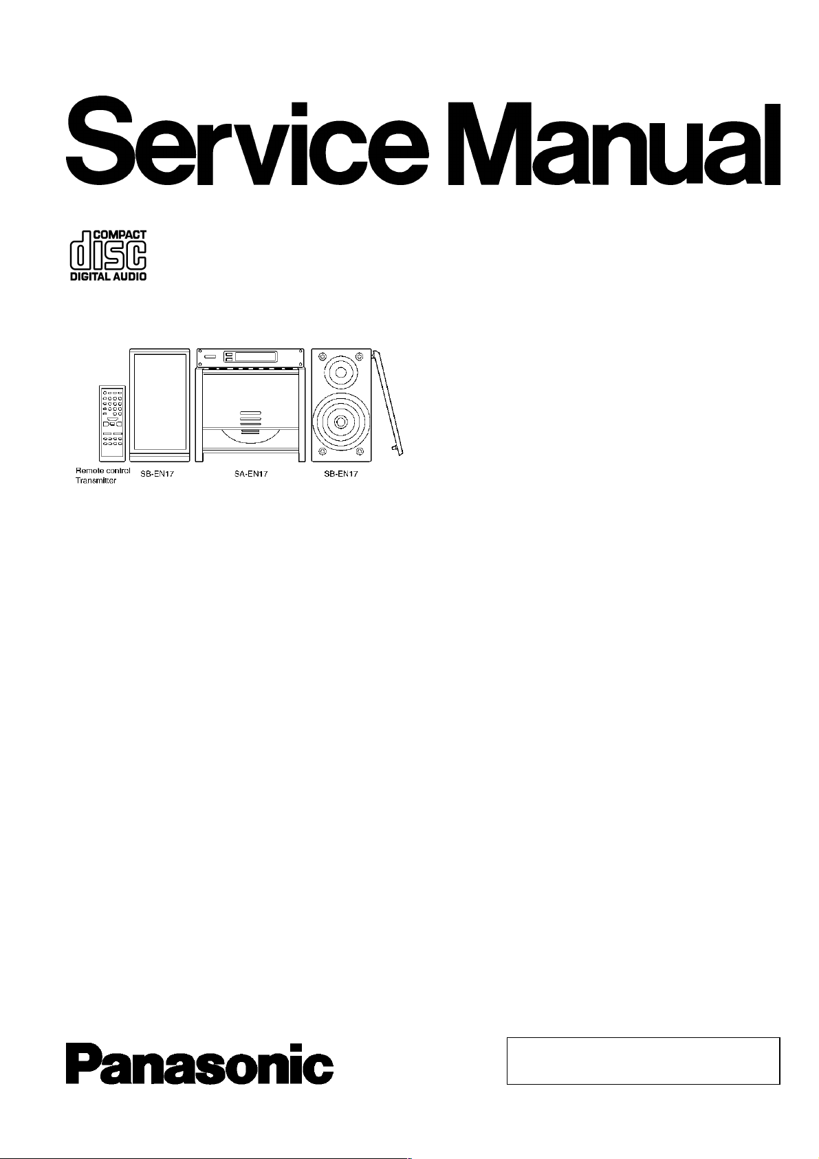
CD Stereo System
SC-EN17E
SC-EN17EB
SC-EN17EG
SC-EN17GCS
SC-EN17GD
Colour
S............Silver Type
ORDER NO.AD0504037CE
Specifications
MAIN UNIT
nRADIO
Frequencyrange:
FM; 87.5 - 108.0 MHz (50kHz steps)
(For E,EB,EG areas)
M; 522 - 1629 kHz (9kHz steps)
(For GCS,GD areas)
M; 522 - 1629 kHz (9kHz steps)
520 - 1630 kHz (10kHz steps)
Intermediate Frequency:
FM; 10.7MHz
(For E,EB,EG areas)
M; 459kHz
(For GCS,GD areas)
M; 450kHz
Sensitivity:
FM; 3.98µV/50mW output (-3dB limit
sens.)
System
lSC-EN17E/EB/EG/GD
Main Unit: SA-EN17E/EB/EG/GD
Speakers: SB-EN17P
lSC-EN17GCS
Main Unit: SA-EN17GCS
Speakers: SB-EN17GCS
M; 178µV/m/50mW output (Ma
sens.)
nCD PLAYE
Sampling frequency: 44.1kHz
Decoding: 16 bit linear
Beam source: Semiconductor laser (wavelength
780nm)
Number of channels: 2 channel, stereo
Wow and flutter: Less than possible measurement
data
DA converter: MASH(1 bit DAC)
nTerminals
Input:
Output: PHONES: 3.5mm stereo (32Ω)
nGENERAL
(For E,EB,EG areas)
Power supply:
(For GCS area)
Power supply:
UX; 3.5mm stereo (27kΩ)
C230V - 240V, 50Hz
C220V - 240V, 50/60Hz
© 2005 Matsushita Electric Industrial Co., Ltd. All
rights reserved. Unauthorized copying and
distribution is a violation of law.
A
SC-EN17E / SC-EN17EB / SC-EN17EG / SC-EN17GC S / SC-EN17GD
(For GD area)
Power supply:
(For E,EB,EG,G D areas)
Power consumptio n: 28W
(For GCS area)
Power consumptio n: 22W
Dimensions (W×H×D): 206×204×214mm
Mass: 4.0kg with speakers
2.4kg without speakers
nSPEAKERS
C220V, 60Hz
(For E,EB,EG,G D areas)
Full range: 8cm, 6Ω×2
(For GCS area)
Full range: 8cm, 12Ω ×2
Ceramic tweeter: 1.52cm ×2
Dimensions (W×H×D): 115mm×211mm×215mm
Power consumptio n in standbymode: 3.1W
Note:
Specifications are subject to change without notice.
Mass and dimensions are approximate.
CONTENTS
Page Page
1 Accessories 2
2 Location of Control
3 Handling Precautions For Traverse Deck (Optical Pickup)
4 Precaution of Laser Diode
5 Protection Circuitry
6 Caution for AC Mains Lead
7 Prevention of Electro Static Discharge (ESD) To
Electrostatically (ES) Devices
8 Handling the Lead-free Solder
8.1. About lead free solder (PbF)
9 Operation Checks and Component Replacement
9.1. Checking for the motor P.C.B., main P.C.B., power AMP
P.C.B., LCD P.C.B., CD servo P.C.B. and tuner P.C.B.
9.2. Replacement for the traverse deck ass 馳
9.3. Replacement for the CD loading motor and optical pick-up
9.4. Replacement for the small DC motor ass 馳
9.5. Replacement for the gear chassis R ass 馳 and gear
chassis L ass 馳
9.6. Replacement for the CD lid unit
9.7. Replacement for the clamper, magnet and fix plate
9.8. Replacement for the CD lid unit A, CD lid unit B and slide
frame
9.9. Replacement for the lid LED lens, LED P.C.B., CD holder
A unit, CD holder A and lift plate
10 Self Diagnostic Function
3
3
4
5
6
7
7
7
8
8
9
10
12
13
14
15
15
16
10.1. Setting of self diagnostic Function
11 Description of Error Code
11.1. Error detection for CD Mechanism block
12 Schematic Diagram
12.1. Schematic Diagram Notes
12.2. Schematic Diagram (SB-EN17)
12.3. Schematic Diagram
13 Printed Circuit Board
14 Block Diagram
15 Wiring Connection Diagram
16 Type Illustrations of ICs, Transistors and Diodes
17 Measurements and Adjustments
17.1. Tuner Adjustment
17.2. Adjustment Point
18 Terminal Functions of ICs
19 Replaceme nt Parts List
19.1. SA-EN17
19.2. SB-EN17P
19.3. SB-EN17GCS
20 Cabinet Parts Location
20.1. SA-EN17
20.2. SB-EN17
21 Packaging
17
17
18
18
19
19
20
21
27
31
35
37
38
38
38
39
40
40
45
45
46
46
48
49
1 Accessories
· Remote control (EUR7711170).....................................1pc.
· Ac power supply cord (RJA0065-1D)............... .............1pc.
· Batteries
· AM loop antenn a (G0ZZ00002036)...............................1 pc.
2
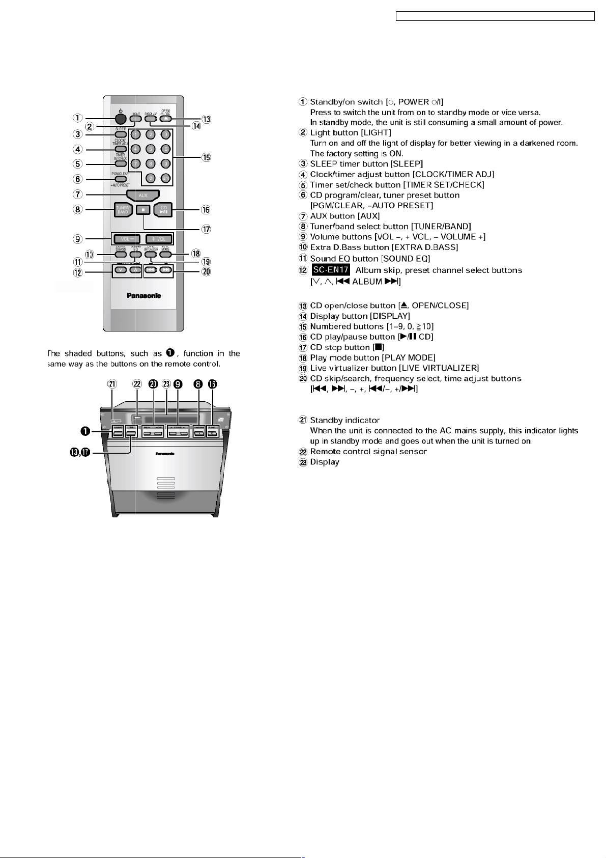
2 Location of Control
SC-EN17E / SC-EN17EB / SC-EN17EG / SC-EN17GC S / SC-EN17GD
3 Handling Precautions For Traverse Deck (Optical
Pickup)
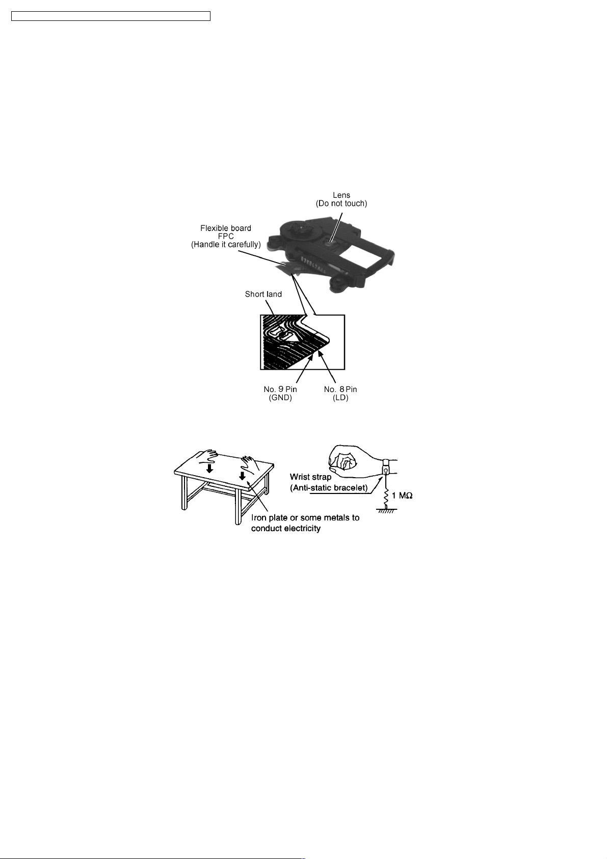
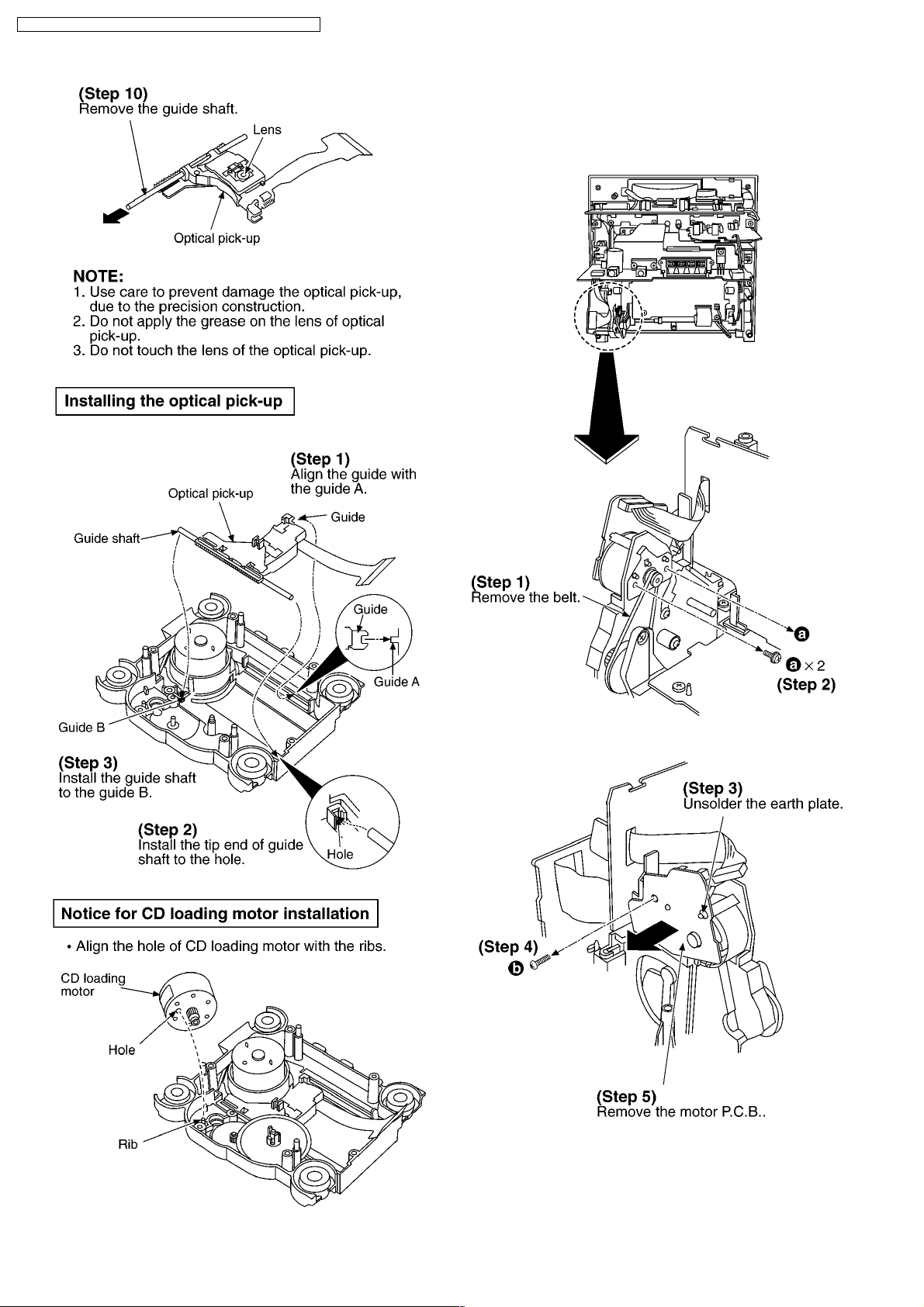
The laser diode in the traverse deck (optical pickup) may break down due to potential caused by static electricity of clothes or
human body. So, be careful of electrostatic breakdown during repair of the traverse deck (optical pickup).
· Handling of traverse deck (optical pickup)
1. Do not subject the traverse deck (optical pickup) to static electricity as it is extremely sensitive to electrical shock.
2. To prevent the breakdown of the laser diode, an antistatic shorting pin is inserted into flexible board (FFC board).(Fig.1)
3. Take care not to apply excessive stress to the flexible board (FFC board). When removing or connecting the short pin, finish
the job in as short time as possible.
4. Do not turn the variable resistor (laser power adjustment). It has already been adjuste d.
· Grounding for electrostatic breakdown prevention
1. Human body grounding (Fig.2)
Use the anti-static wrist strap to discharge the static electricity from your body.
2. Work table grounding (Fig.2)
3
SC-EN17E / SC-EN17EB / SC-EN17EG / SC-EN17GC S / SC-EN17GD
Put a conduc tive material (sheet) or steel sheet on the area where the traverse deck (optical pickup) is place, and ground
the sheet.
Caution:
The static electricity of your clothes will not be grounded through the wrist strap. So, take care not to let your clothes touch
the traverse deck (optical pickup).
Caution when replacing the Traverse Deck
The traverse deck has a short point shorted with solder to protect the laser diode against electrostatics breakdown. Be sure
to remove the solder from the short point before making connections.
(Fig.1)
(Fig.2)
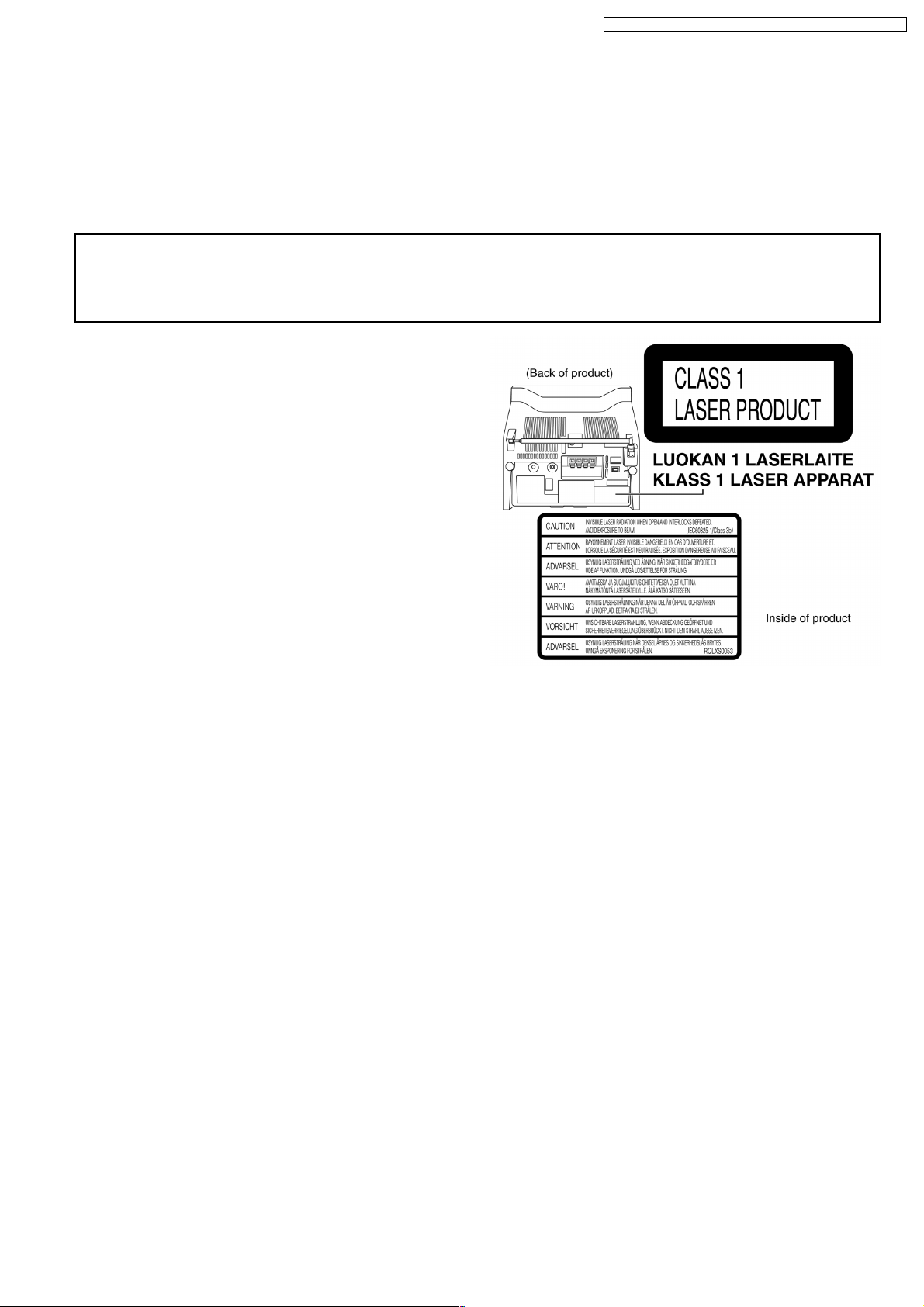
4 Precaution of Laser Diode
Caution :
This product utilizes a laser diode with the unit turned "ON", invisible laser radiation is emitted from the pick up lens.
Wavelength : 780 nm
Maximum output radiation power from pick up : 100 µW/VDE
Laser radiation from pick up unit is safety level, but be sure the followings:
1. Do not disassemble the optical pick up unit, since radiation from exposed laser diode is dangerous.
2. Do not adjust the variable resistor on the pick up unit. It was already adjusted.
3. Do not look at the focus lens using optical instruments.
4. Recommend not to look at pick up lens for a long time.
ACHTUNG :
Dieses Produkt enthält eine Laserdiode. Im eingeschalteten Zustand wird unsichtbare Laserstrahlung von der Lasereinheit
abgestrahlt.
Wellenlänge : 780nm
Maximale Strahlungsleistung der Lasereinheit :100 µW/VD E
4
SC-EN17E / SC-EN17EB / SC-EN17EG / SC-EN17GC S / SC-EN17GD
Die Strahlung an der Lasereinheit ist ungefährlich, wenn folgende Punkte beachtet werden:
1. Die Lasereinheit nicht zerlegen, da die Strahlung an der freigelegten Laserdiode gefährlich ist.
2. Den werkseitig justierten Einstellregler der Lasereinhit nicht verstellen.
3. Nicht mit optischen Instrumenten in die Fokussierlinse blicken.
4. Nicht über längere Zeit in die Fokussierlinse blicken.
ADVARSEL: I dette a apparat anvendes laser.
CAUTION!
THIS PRODUCT UTILIZES A LASER.
USE OF CONTROLS OR ADJUSTMENTS OR PERFORMANCE OF PROCEDURES OTHER THAN THOSE SPECIFIED HEREIN MAY RESULT
IN HAZARDOUS RADIATION EXPOSURE.
n Use of caution label
5 Protection Circuitry
The protection circuitry may have operated if either of the following conditions are noticed:
· No sound is heard when the power is turned on.
· Stop during a perform ance.
The function of this circuitry is to prevent circuitry damage if, for example, the positive and negative speaker connection wires
are “shorted”, or if speaker with an impedance less than the indicated rated impedance of the amplifier are used.
If this occurs, follow the procedure outline below:
1. Turn off the power.
2. Determine the cause of the problem and correct it.
3. Turn on the power once again after one minute.
Note:
When the protection circuitry functions, the unit will not operate unless the power is first turned off and then on again.
5
SC-EN17E / SC-EN17EB / SC-EN17EG / SC-EN17GC S / SC-EN17GD
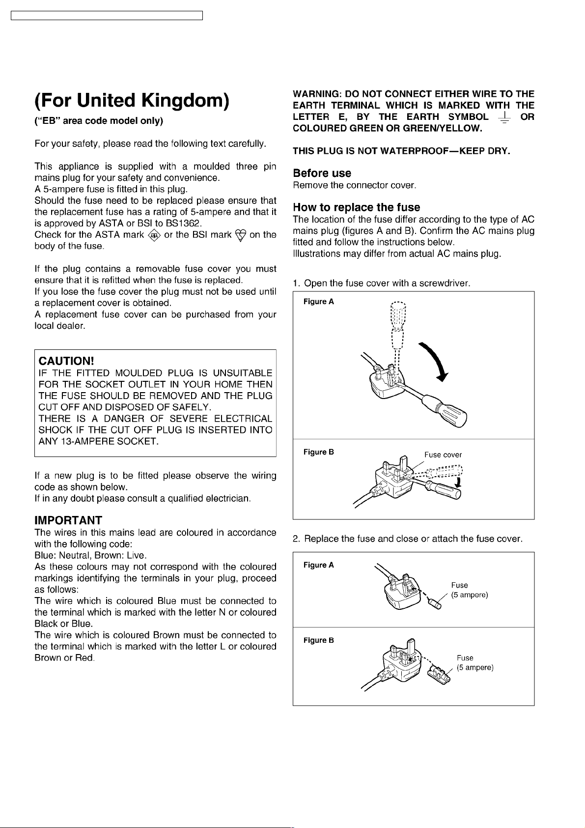
6 Caution for AC Mains Lead
6

SC-EN17E / SC-EN17EB / SC-EN17EG / SC-EN17GC S / SC-EN17GD
7 Prevention of Electro Static Discharge (ESD) To
Electrostatically (ES) Devices
Some semiconductor (solid state) devices can be damaged easily by static electricity. Such components commonly are called
Electrostatically Sensitive (ES) Devices. Examples of typical ES Devices are integrated circuits and some field-effect transistors
and semiconductor “chip” components. The following techniques should be used to help reduce the incidence of component
damage caused by electro static discharge (ESD).
1. Immediately before handling any semiconductor component or semiconductor-equipped assembly, drain off any ESD on your
body by touching a known earth ground. Alternatively, obtain and wear a commercially available discharging ESD wrist strap,
Which should be removed for potential shock resons prior to applying power to the unit under test.
2. After removing an electrical assembly equipped with ES devices, place the assembly on a conductive surface such as alminum
foil, to prevent electrostatic charge buildup or exposure of the assembly.
3. Use only a grounded-tip soldering iron to solder or unsolder ES devices.
4. Use only an anti-static solder removal devices. Some solder removal devices not classified as “anti-static (ESD protected)” can
generate electrical charge sufficient to damage ES devices.
5. Do not use freon-propelled chemicals. These can generate electrical charges sufficient to damage ES devices.
6. Do not remove a replacement ES device from its protective package until immediately before you are ready to install it. (Most
replacement ES devices are packaged with leads electrically shorted together by conductive foam, alminum foil or comparable
conductive material).
7. Immediately before removing the protective material from the leads of a replacement ES device, touch the protective material
to the chassis or circuit assembly into which the device will be installed.
Caution
Be sure no power is applied to the chassis or circuit, and observe all other safety precautions.
8. Minimize bodily motions when handling unpackaged replacement ES devices.(Otherwise harmless motion such as the brushing
together of your clothes fabric or the lifting of your foot from a carpeted floor can generate static electricity (ESD) sufficient to
damage an ES device).
8 Handling the Lead-free Solder
8.1. About lead free solder (PbF)
Distinction of PbF P.C.B.:
P.C.B.s (manufactured) using lead free solder will have a PbF stamp on the P.C.B.
Caution
· Pb free solder has a higher melting point than standard solder; Typically the melting point is 50-70°F (30 - 40°C)
higher.Please use a high temperature soldering iron. In case of the soldering iron with temperature control, please set it to
700± 20 °F (370 ± 10°C).
· Pb free solder will tent to splash when heated too high (about 1100°F/600°C).
· W hen soldering or unsoldering, please completely remove all of the solder on the pins and solder area, and be sure to heat
the soldering points with the Pb free solder until it melts enough.
7
SC-EN17E / SC-EN17EB / SC-EN17EG / SC-EN17GC S / SC-EN17GD
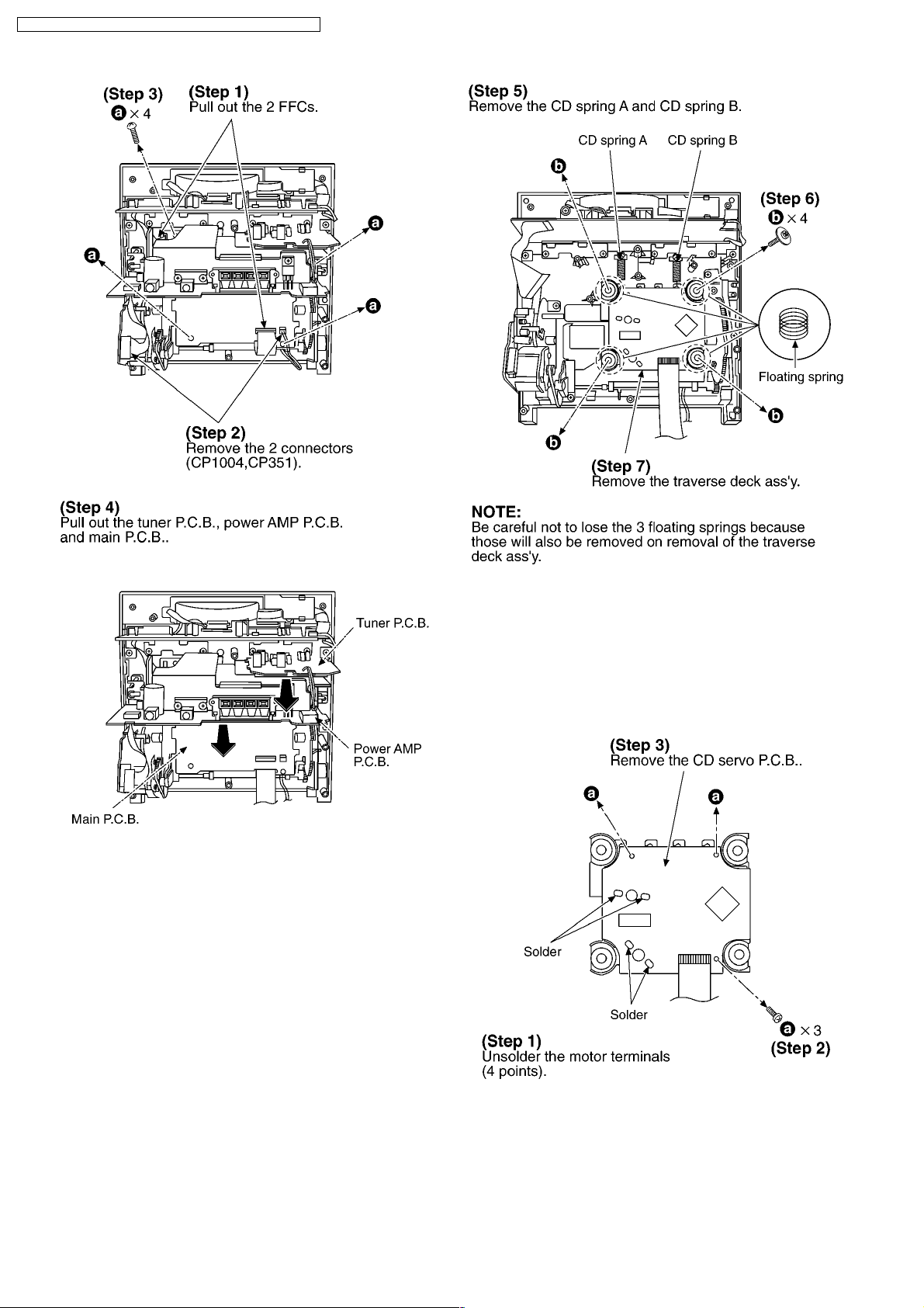
9 Operation Checks and Component Replacement
· This section desceibes procedures for checking the
operation of the major printed circuit boards and replacing
the main components.
· For reassembly after operation checks or replacement,
reverse the respective procedures. Special reassembly
procedures are described only when required.
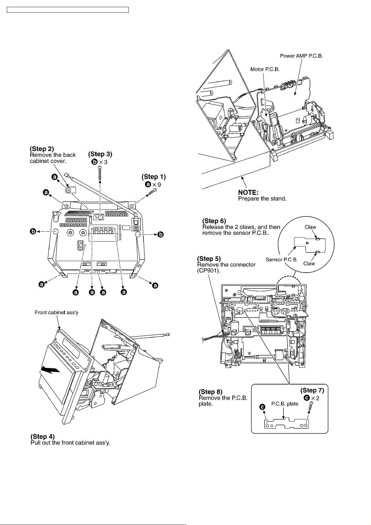
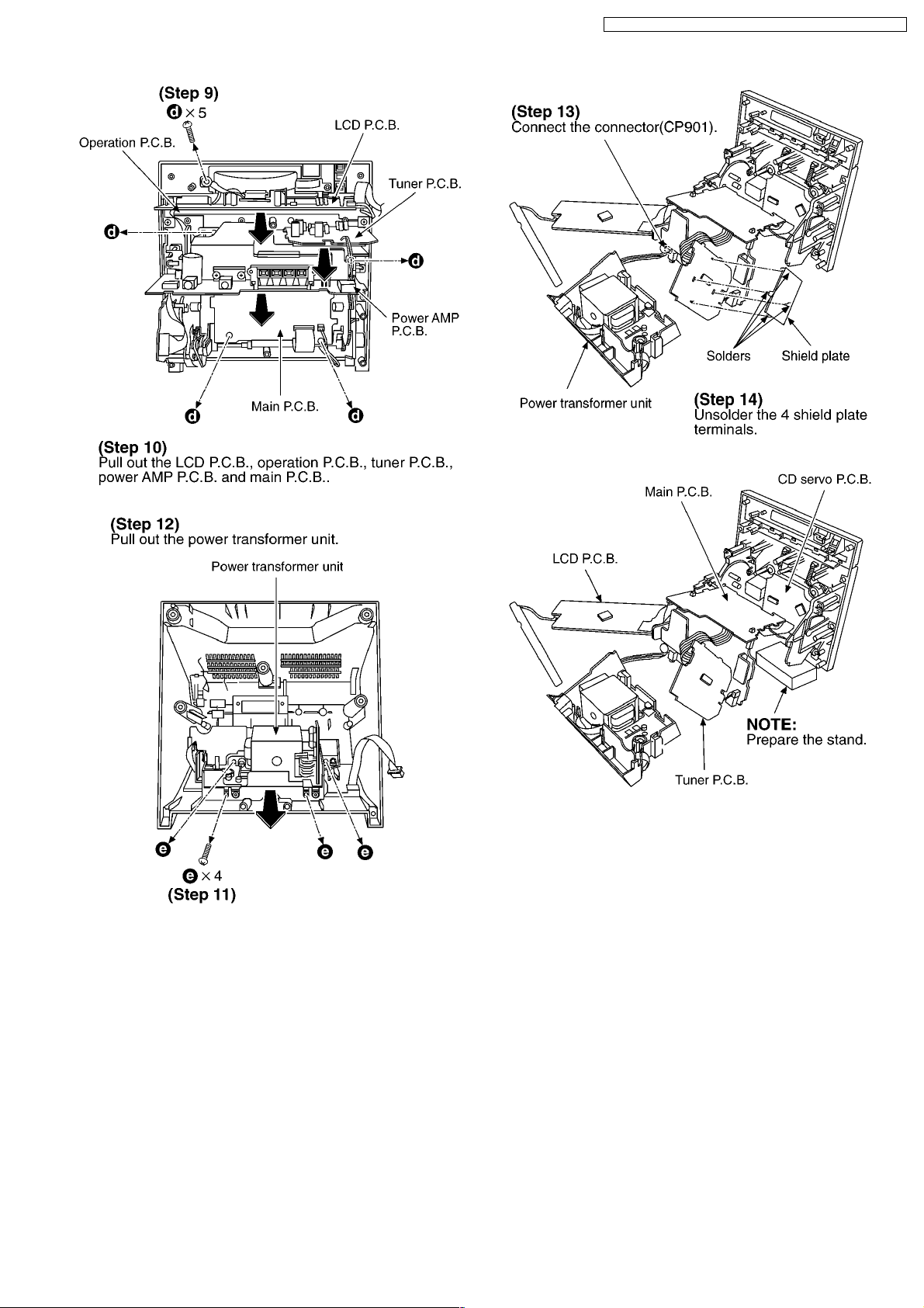
9.1. Checking for the motor P.C.B.,
main P.C.B., power AMP
P.C.B., LCD P.C.B., CD servo
P.C.B. and tuner P.C.B.
· Check the motor P.C.B. and power AMP P.C.B. as shown
below.
8
SC-EN17E / SC-EN17EB / SC-EN17EG / SC-EN17GC S / SC-EN17GD
9.2. Replacement for the traverse
deck ass’y
· Follow the (Step 1) - (Step 5) of Item 9.1.
9
SC-EN17E / SC-EN17EB / SC-EN17EG / SC-EN17GC S / SC-EN17GD
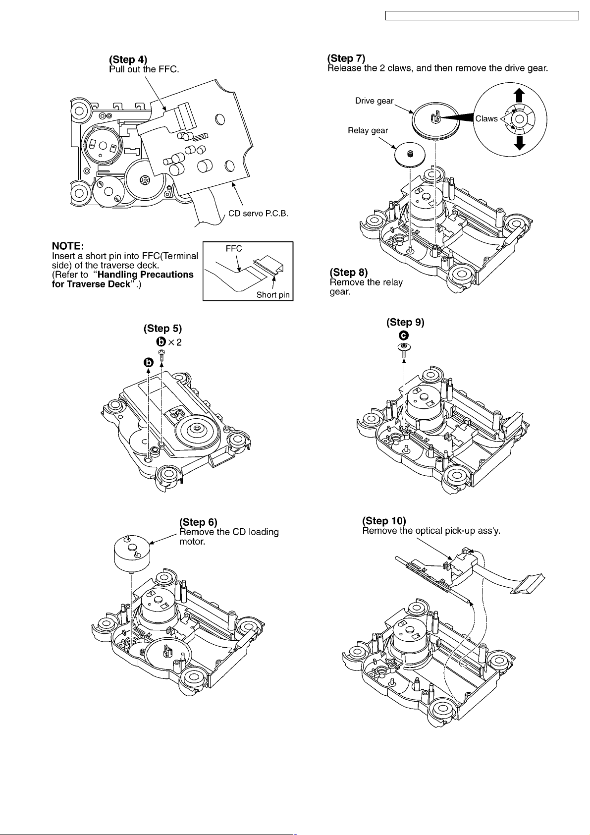
9.3. Replacement for the CD
loading motor and optical
pick-up
· Follow the (Step 1) - (Step 5) of item 9.1.
· Follow the (Step 1) - (Step 7) of item 9.2.
10
SC-EN17E / SC-EN17EB / SC-EN17EG / SC-EN17GC S / SC-EN17GD
11
SC-EN17E / SC-EN17EB / SC-EN17EG / SC-EN17GC S / SC-EN17GD
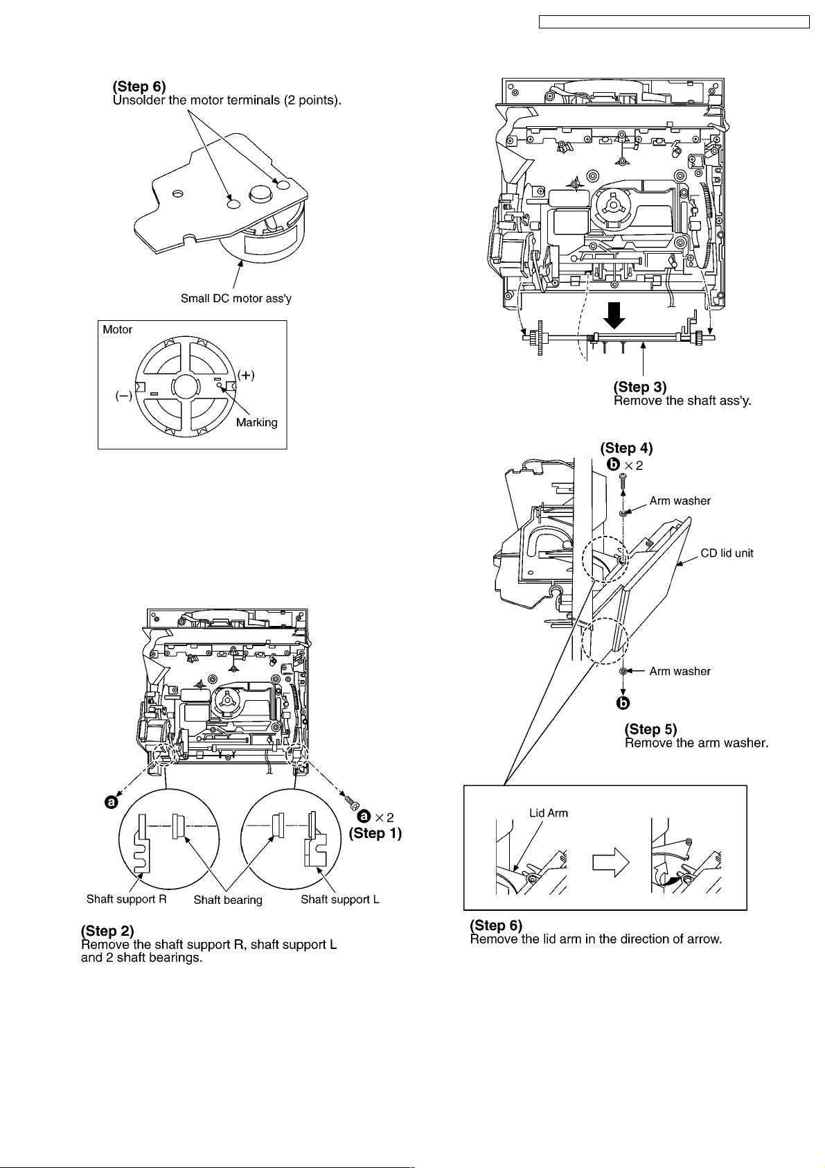
9.4. Replacement for the small DC
motor ass’y
· Follow the (Step 1) - (Step 5) of item 9.1.
12
SC-EN17E / SC-EN17EB / SC-EN17EG / SC-EN17GC S / SC-EN17GD
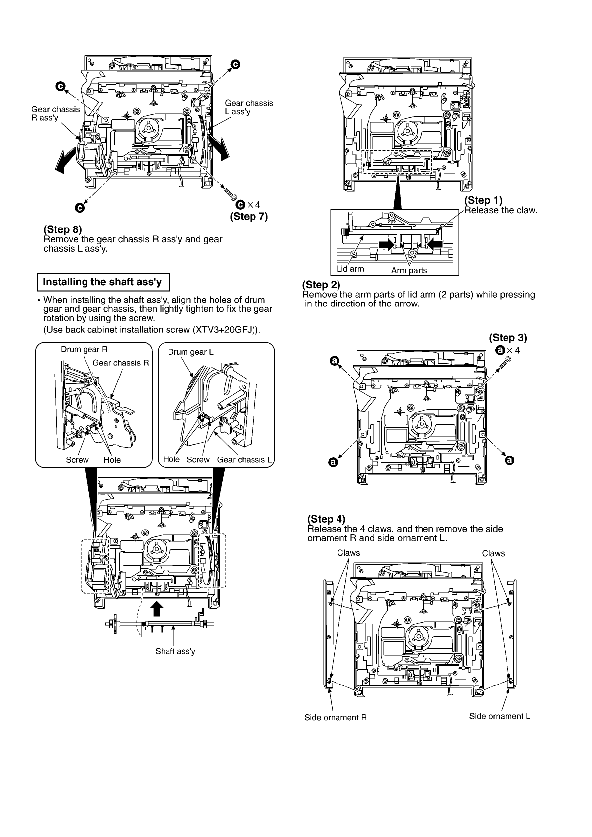
9.5. Replacement for the gear
chassis R ass’y and gear
chassis L ass’y
· Follow the (Step 1) - (Step 5) of item 9.1.
· Follow the (Step 1) - (Step 7) of item 9.2.
13
SC-EN17E / SC-EN17EB / SC-EN17EG / SC-EN17GC S / SC-EN17GD
9.6. Replacement for the CD lid
unit
· Follow the (Step 1) - (Step 5) of item 9.1.
· Follow the (Step 1) - (Step 7) of item 9.2.
· Follow the (Step 1) - (Step 8) of item 9.5.
14
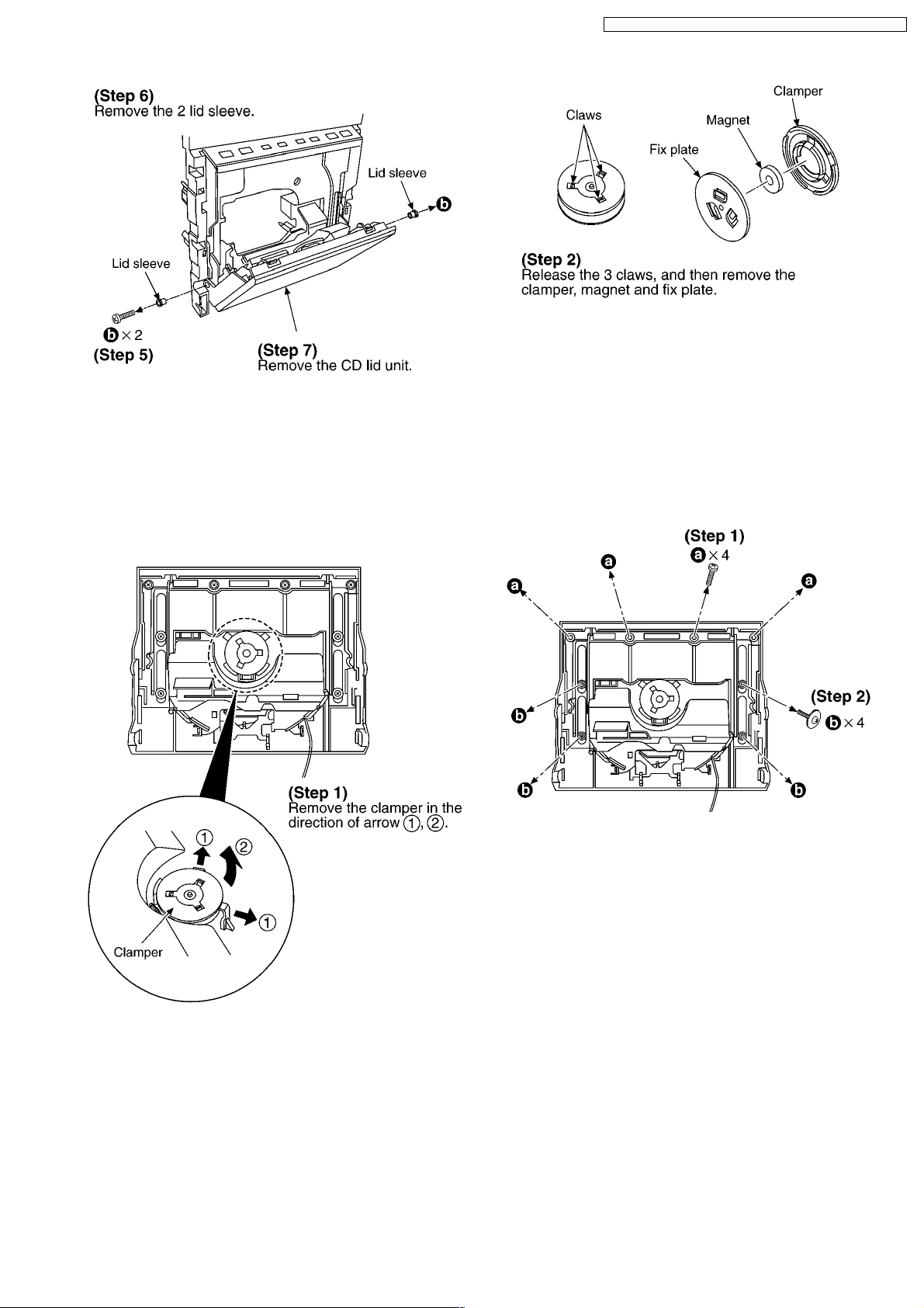
9.7. Replacement for the clamper,
magnet and fix plate
· Follow the (Step 1) - (Step 5) of item 9.1.
· Follow the (Step 1) - (Step 7) of item 9.2.
· Follow the (Step 1) - (Step 8) of item 9.5.
· Follow the (Step 1) - (Step 7) of item 9.6.
SC-EN17E / SC-EN17EB / SC-EN17EG / SC-EN17GC S / SC-EN17GD
9.8. Replacement for the CD lid
unit A, CD lid unit B and slide
frame
· Follow the (Step 1) - (Step 5) of item 9.1.
· Follow the (Step 1) - (Step 7) of item 9.2.
· Follow the (Step 1) - (Step 8) of item 9.5.
· Follow the (Step 1) - (Step 7) of item 9.6.
15
 Loading...