

Page 1
Model No. PDP-2012
Hints for SC/SN Board Repair
( PDP 2012 - 2010 model )
Order No. ITD1212911GE
PDP-2011
PDP-2010
Issue date : Dec. 2012
c
Panasonic Corporation 2012
Unauthorized copying and distribution is
a violation of law.
1
Page 2
< Caution >
1. (HD model = X/C/A series only)
Before checking the SN board with the TV set,
check all key components with multi meter.
Depending on the defective area of SN board,
SS board damage may occur.
2. All key components must be checked and
all defective components must be replaced at the same time.
If some defective components remain,
other components may become damaged again.
3. When assembling the SN/SC board to the TV set,
the screws must be properly fastened.
If screws are loosely tightened, there is a possibility
of shutdown or board damage.
2
Page 3

Contents
1.Block Diagram ( Difference of ’10/’11/’12 )
< 2012 model >
2-1.Explanation of Scan Board Operation and Check Point
2-2.Check List
2-3.Repair Data
< 2011 model >
3-1.Explanation of Scan Board Operation and Check Point
3-2.Check List
3-3.Repair Data
< 2010 model >
4-1.Explanation of Scan Board Operation and Check Point
4-2.Check List
4-3.Repair Data
3
Page 4

1.Block Diagram ( Difference of ’10/’11/’12 )
4
Page 5
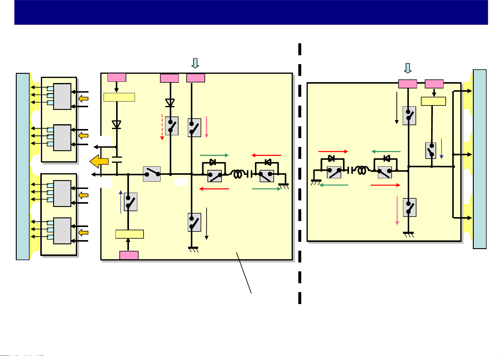
Panel drive ( 2012/2011 Full-HD model (except 42inch) )
SU
SU
Vscn Gen.
VFO
VFG
VSUS
VSUS
P board
VSUS
VOL
SC
SC
SS
SS
P board
VSUS
VSUS
Ve Gen.
PDP panel
SD
SD
< 2012 model >
< 2011 model >
Vad Gen.
VSUS
T*-P42GT50/ST50* :TNPA5523**
T*-P42UT50* :TNPA5620**
T*-P42 ST30/UT30/S30/U30* : TNPA5349**
T*-P42 VT30/GT30* : TNPA5330**
T*-P42 G30 : TNPA5457**
PDP panel
5
Page 6
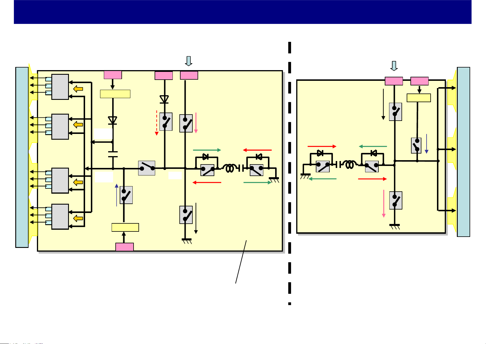
Panel drive ( 2012/2011 42inch Full-HD model )
VSUS
Vscn Gen.
VFO
VFG
VSUS
P board
VSUS
VOL
SN
SN
SS
SS
P board
VSUS
VSUS
Ve Gen.
PDP panel
< 2012 model >
< 2011 model >
Vad Gen.
VSUS
T*-P42GT50/ST50* :TNPA5523**
T*-P42UT50* :TNPA5620**
T*-P42 ST30/UT30/S30/U30* : TNPA5349**
T*-P42 VT30/GT30* : TNPA5330**
T*-P42 G30 : TNPA5457**
PDP panel
6
Page 7
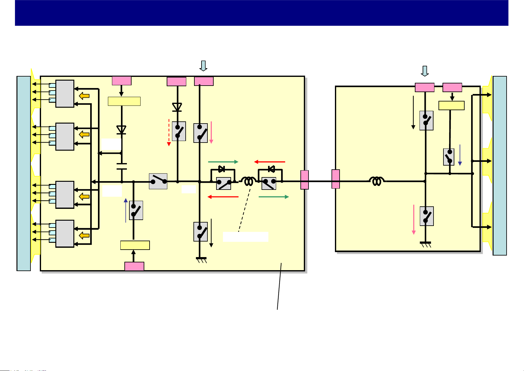
Panel drive ( 2012/2011 HD model )
VSUS
Vscn Gen.
VFO
VFG
VSUS
P board
VSUS
VOL
SN
SN
MID
SS
SS
P board
VSUS
VSUS
Ve Gen.
PDP panel
< 2012 model >
< 2011 model >
( only 2011 )
Vad Gen.
VSUS
T*-P42X5/X50/C5/C50*, TC-P46X5* :TNPA5592**
T*-P50X5/X50/C5/C50* :TNPA5593**
T*-P42X3/X30/C3/C30*, TC-P46X3* : TNPA5311**
T*-P50X3/X30/C3/C30* : TNPA5312**
PDP panel
7
Page 8
Panel drive ( 2010 Full-HD model )
SM board (only 42inch)
Vscn Gen.
VFO
SU
SU
VFG
VSUS
VSUS
VOL
P board
VSUS
SC
SC
SS
SS
P board
VSUS
VSUS
Ve Gen.
Vad Gen.
SD
SD
PDP panel
T*-P42/46/50/55 VT20/VT25/GT20/GT25/V20/G20/G25/S20/S2* : TNPA5081**
T*-P42/46/50 S20/S25/S2/U20/U2* : TNPA5105**
T*-P58/65 VT20/VT25/S20/S2* : TNPA5175**
VSUS
PDP panel
8
Page 9
Panel drive ( 2010 50/37inch HD model )
P board
P board
SU
SU
SD
SD
VSUS
Vscn Gen.
VFO
VFG
Vad Gen.
VSUS
VSUS
VOL
VSUS
SC
SC
SC3 SS3
MID
SS
SS
VSUS
VSUS
Ve Gen.
PDP panel
PDP panel
T*-P50 C2/X2/X20* : TNPA5063**
TX-P37 C2/X20/X25* : TNPA5062**
9
Page 10
Panel drive ( 2010 42/46inch HD model )
P board
P board
VSUS
Vscn Gen.
VFO
VFG
Vad Gen.
VSUS
VOL
VSUS
SN
SN
SN3 SS3
MID
SS
SS
VSUS
VSUS
Ve Gen.
PDP panel
VSUS
T*-P42X2/X20/C2/C20/A20*, TC-P46C2* : TNPA5066**
PDP panel
10
Page 11

< 2012 model >
2-1.Explanation of Scan Board Operation
and Check Point
11
Page 12
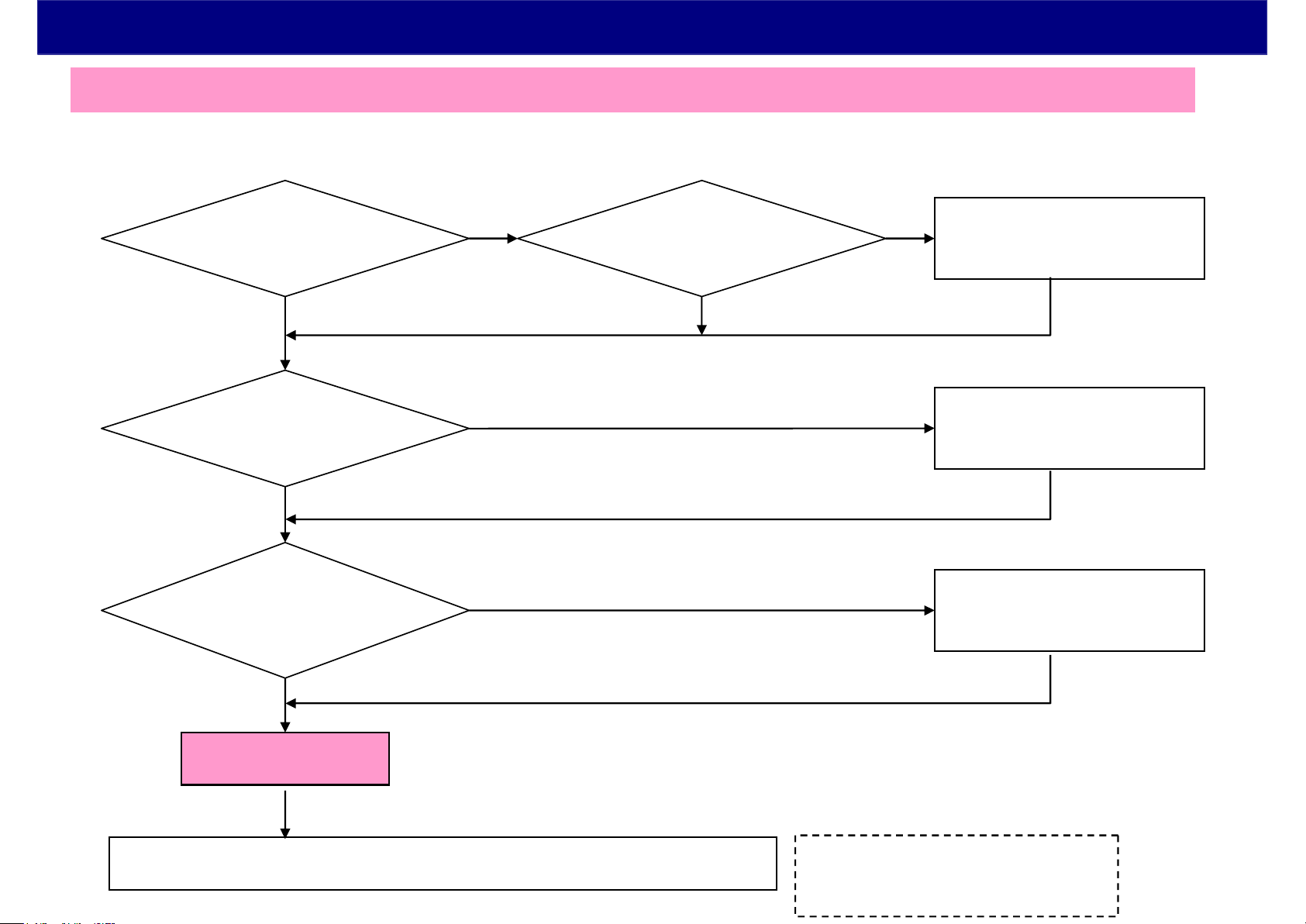
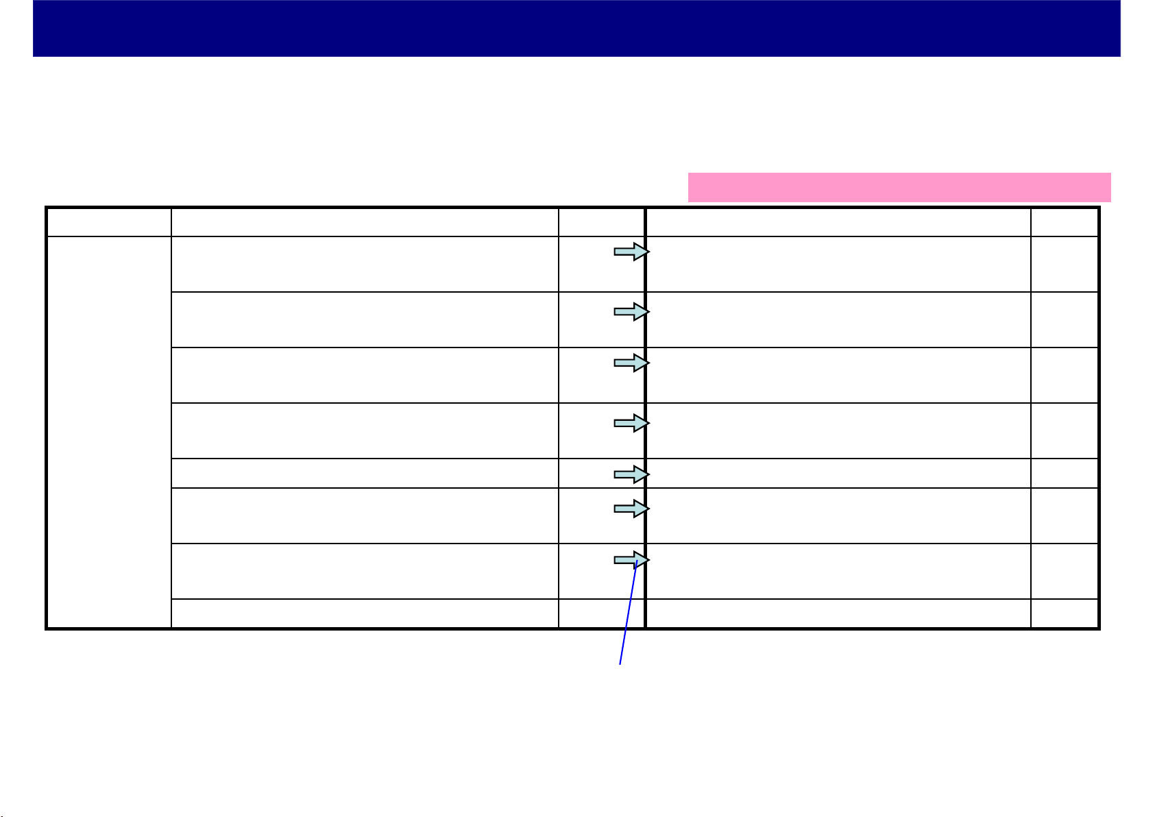
Check Flow of SC/SN Board Repair
< 2012 model >
Before power-on for checking, replace all defective components in BLOCK 1, 2 and 3.
Block1.
Check of IGBT/Tr (C-E),
FET (S-D) and Diode
All OK
Block2.
Check of Scan Drive IC
(Only SN board)
All OK
Block3.
Check of power circuit
Shorted
Shorted
Shorted
Block1
Check also control
signal drive circuit
All OK
Shorted
Replace the defective
components
Replace the defective
components
Replace the defective
components
All OK
Power on check
After replacing all defective component,
Check with power. (especially HD model)
NG
Other Block. Check the SOS circuit and feed back circuit
Check the control signals
( Photo Coupler )
12
Page 13
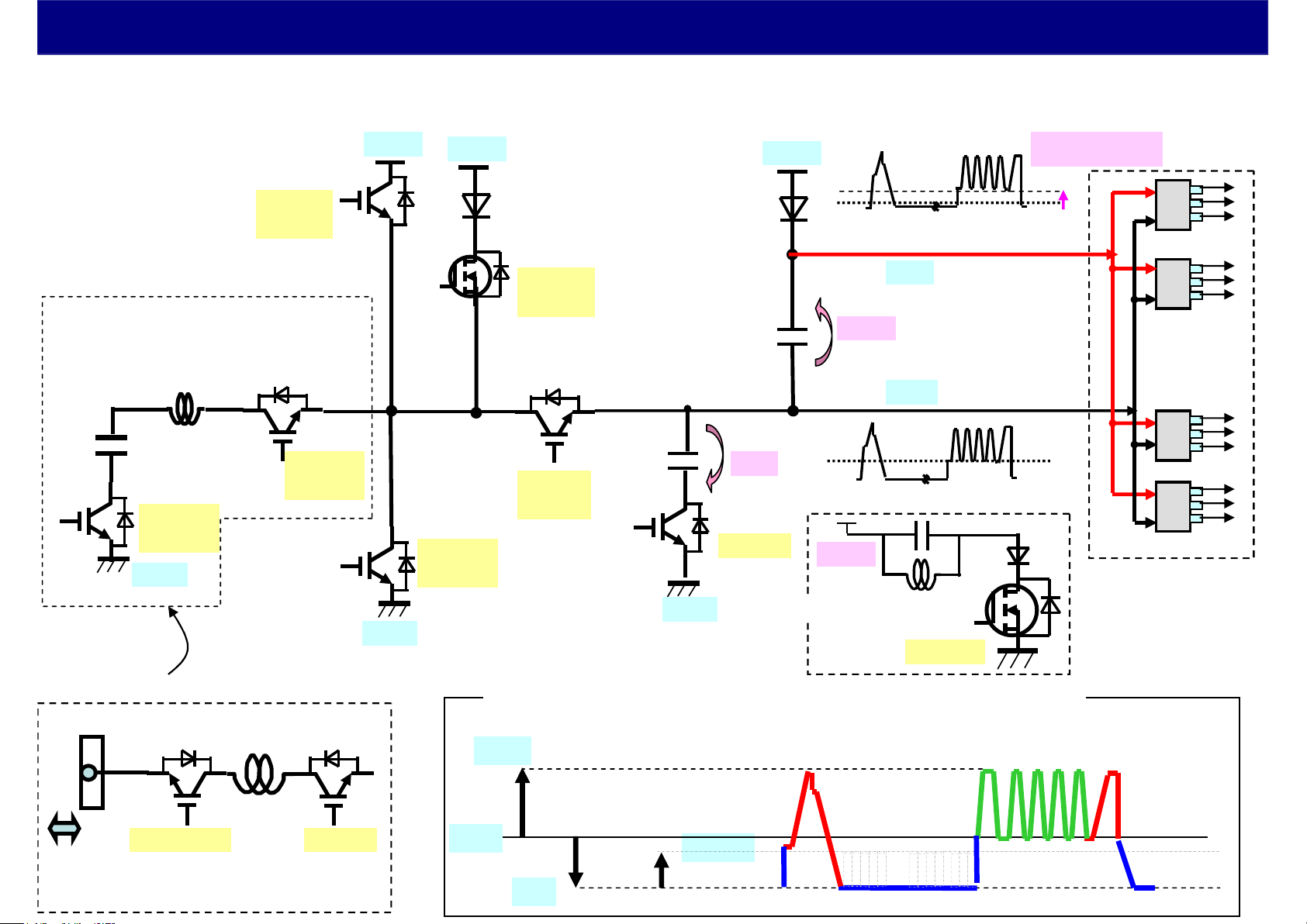
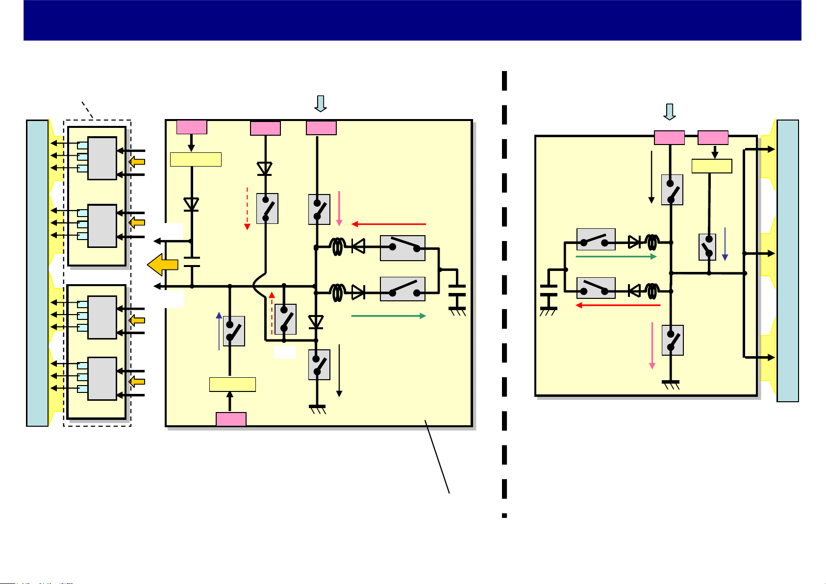
Block Diagram of Scan Pulse Drive
< 2012 model >
Scan pulse output waveform is produced by switching of Vsus/Vad/GND.
( Energy recovery circuit )
C16631-
632
L16411-
Q16451
-452
GND
12
Q16401
- 403
Q16441
-443
Vsus
GND
Vsus
VOL
Q16421
-423
Q16600
-601
Q16621
-623
C16813
-
+
GND
Vscn
+
-
Vad
Q16661
VF0
Vscn
C16842
VFG
Vad2
Full-HD model only
Q16660
Vscn shifted
.
.
.
Only SN board
(SC board is
separated to
SU/SD board)
SN board of HD model (not Full-HD model)
SN2
To
PSS
board
L16441
Q16451
D16481D16461
Q16441
< VFG waveform (VFO is added Vscn voltage to VFG) >
Vsus
GND
(Vscn)
Vad
13
Page 14
Block1. Short Circuit Check of the Switching Component and Diode
< 2012 model >
Check the short circuit “all” of the below switching components.
( just check short or not )
In many cases, there are several defective components at the same time.
Check parts ( Defective parts )
:FET(D-S) , Transistor (C-E) , Diode (K-A)
Q16401 - 404 / D16401 - 404
Q16421 - 424 / D16421 - 424
Q16621 - 625 / D16641 - 644
Q16661 / D16673 - 674
Q16660 / D16652 Full HD Only
Q16600 - 601 / D16618, R16601 ( open check)
Q16441 - 443 / D16481 - 483
Q16451 - 453 / D16461 - 463
D16430, D16432, D16434, D16435
D16430, D16432
D16722, D16723, D16725
The Scan board is producing the scan pulse output (VFO and VFG) by switching of
several kinds of voltage. ( refer to the next page )
In main case of the defect, these switching parts are short-circuited.
14
Page 15
BLOCK1 Drive Circuit ( Switching Control Signal )
If drive IC is defect (=always output switch-on signal), the switching component
must be damaged. Check also the drive circuit when the switching component is defect.
< 2012 model >
< example: IC16501,16521 >
IC16501
Buffer (Drive IC)
IN OUT
VOL+15V
VOL
IC16521
Buffer (Drive IC)
VDD
(GND)
R
C
If these switching
components are defect,
check also Drive
components.
Vsus
Q
VOL
Vsus
VOL
GND
VOL
15V
GND
VDD
Q
IN OUT
R
VS
C
15
Page 16
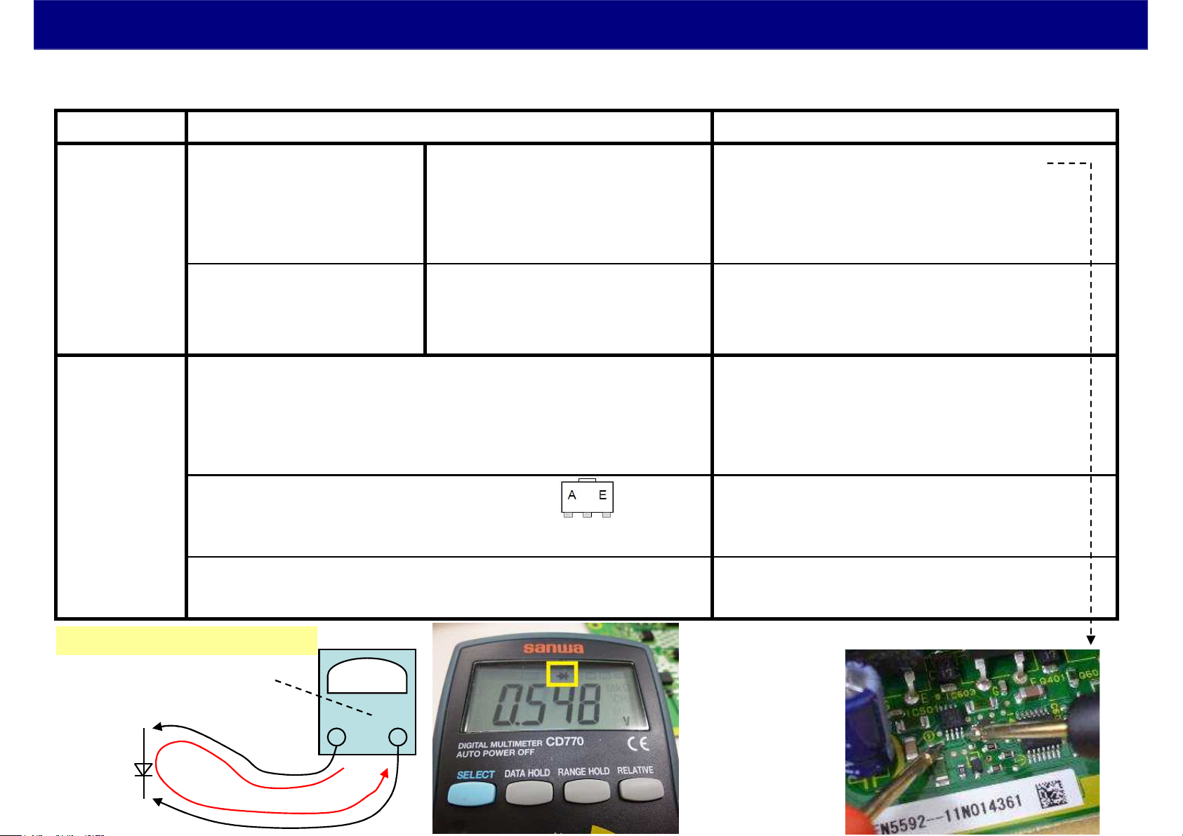
How to check the Drive ICs and Power IC
We can check the power IC and drive IC by DIODE CHECK.
The check terminal is as below.
< 2012 model >
BLOCK1
BLOCK3
(Explanation
is as later
page)
IC
Except
T*-P42GT50/ST50/UT50
(Except TNPA5523/5620)
Only
T*-P42GT50/ST50/UT50
(TNPA5523/5620)
IC16784, IC16786
(power IC)
IC16795
(power IC)
IC16501, 16502, 16521, 16522
(IC15603,16504,16523,16524)
(Drive signal for
switching components)
IC16501, 16502, 16521, 16522
(Drive signal for
switching components)
1 2 3
Vout com Vin
Diode check ( Check pin : Normal voltage )
1pin (+) and 4 pin(-) : 0.45V +/- 0.2V
1pin (+) and 7 pin(-) : 0.45V +/- 0.2V
1pin (+) and 8 pin(-) : 0.5V +/- 0.2V
3pin (+) and 1 pin(-) : 0.5V +/- 0.2V
3pin (+) and 2 pin(-) : 0.55V +/- 0.2V
3pin (+) and 7 pin(-) : 0.55V +/- 0.2V
8pin (+) and 1 pin(-) : 0.45V +/- 0.2V
8pin (+) and 3 pin(-) : 0.6V +/- 0.2V
8pin (+) and 4 pin(-) : 0.6V +/- 0.2V
8pin (+) and 5 pin(-) : 0.45V +/- 0.2V
2pin (+) and 1 pin(-) : 0.5V +/- 0.2V
2pin (+) and 3 pin(-) : 0.45V +/- 0.2V
IC16725
(power IC)
Don’t mistake the polarity.
Diode check
i
12pin (+) and 1 pin(-) : 0.5V +/- 0.2V
12pin (+) and 24 pin(-) : 0.4V +/- 0.2V
example
0.6V
+ -
16
Page 17
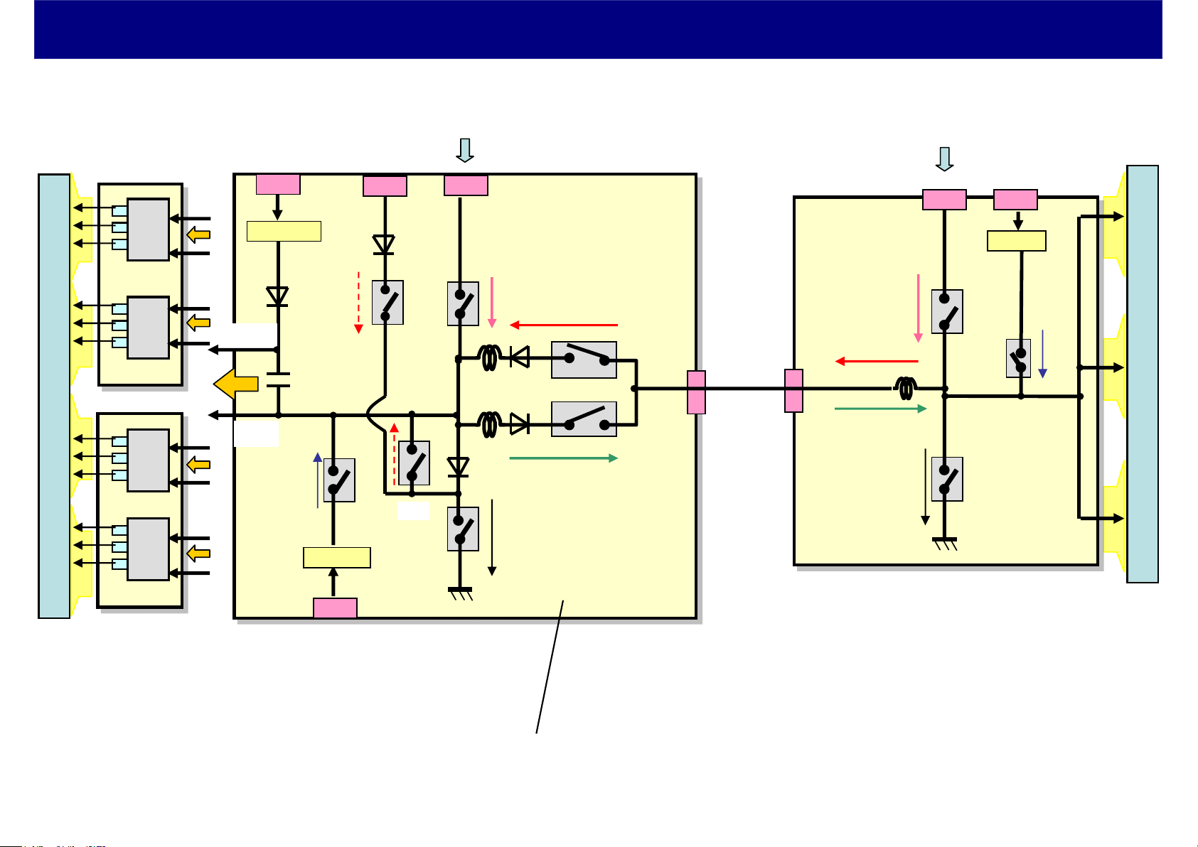
Block2. Short circuit check of Scan Drive IC (Only SN Board)
< 2012 model >
Check the short circuit between VFG and VFO. If shorted, some of the Scan Drive IC is
defective. You can find the defective IC by checking the short circuit between VFG and
all output pin of Scan Drive IC (same as all pin of Connector SN11-18/21-28).
IC14901
Scan
Drive
IC
Scan
Drive
IC
IC14902
IC14953
Scan
Drive
IC
Scan
Drive
IC
( Energy recovery circuit )
C16631-
632
L16411
Q16451
-452
GND
-12
Q16401
- 403
Q16441
-443
Vsus
Vsus
VOL
Q16421
-423
Q16600
-601
Q16621
-623
Vscn
TPSC1/
TPSN1
VF0
+
Vscn
-
-
VFG
Vad
+
Q16661
SN11/21
SN12/22
.
.
.
.
.
.
Output pin
SN17/27
SN18/28
GND
SN board of HD model (not full-HD model)
SN2
To
PSS
board
L16441
Q16451
D16481D16461
Q16441
GND
Check short circuit
(refer to next page)
IC14954
Scan Drive IC
Only SN board
(SC board is
separated to
SU/SD board)
Output pin
17
Page 18
BLOCK2. Short circuit check of Scan Drive IC (Only SN Board)
All
Output
pin
VF_G
18
Page 19
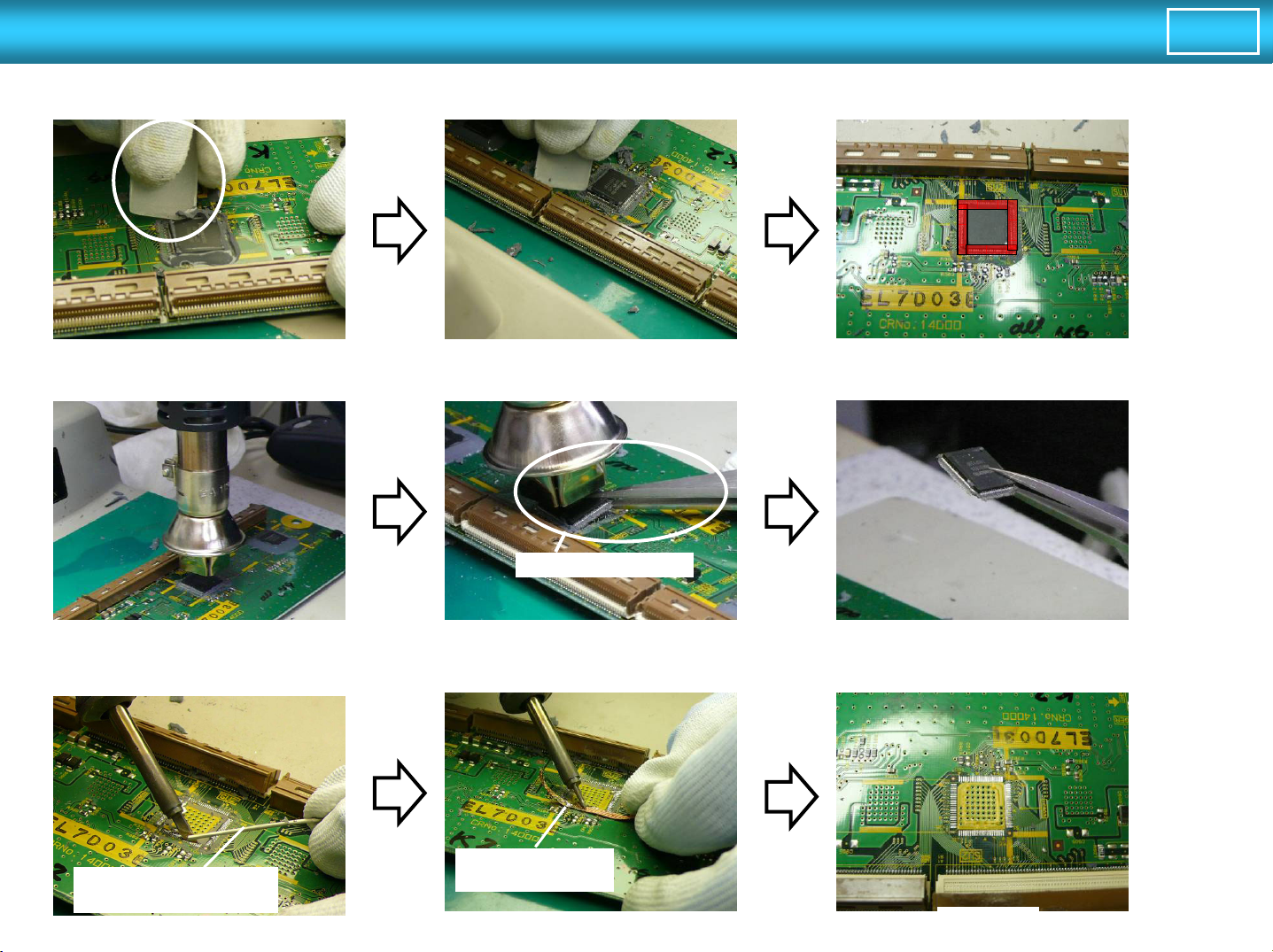
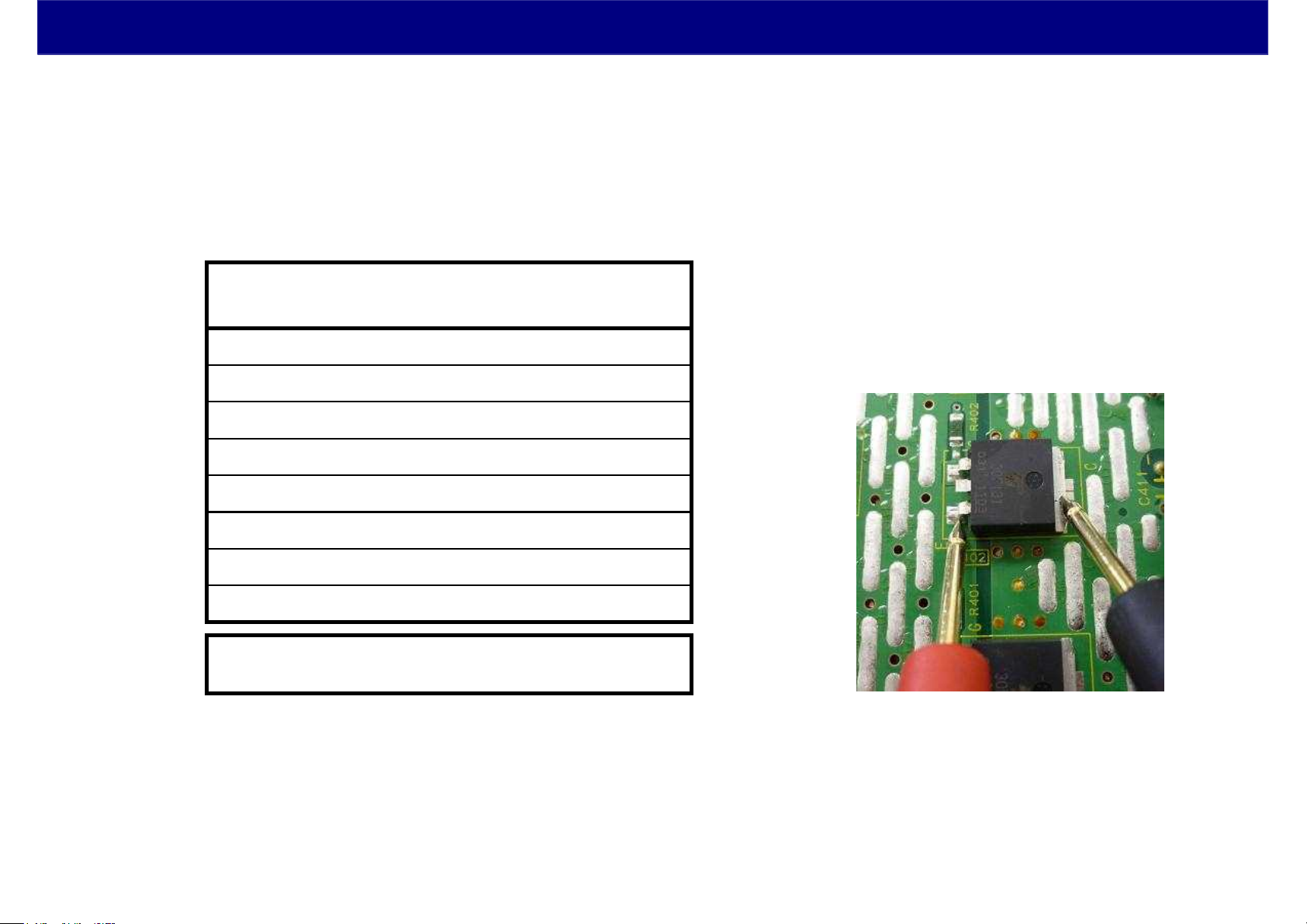
How to replacement of PDP Scan Driver IC on SN board
How to replacement of PDP Scan Driver IC on SN board
1/2
1. Remove silicon glue by plastic plate.
3. Remove IC
Remove by tweezers
2. After removal, put the low temperature
solder
(Part No.:RFKZ0316) on to the solder of IC.
4. Cleaning
Low temperature solder
(Part No.: RFKZ0316)
Blotting wire
(Local procurement)
Completion
Page 20
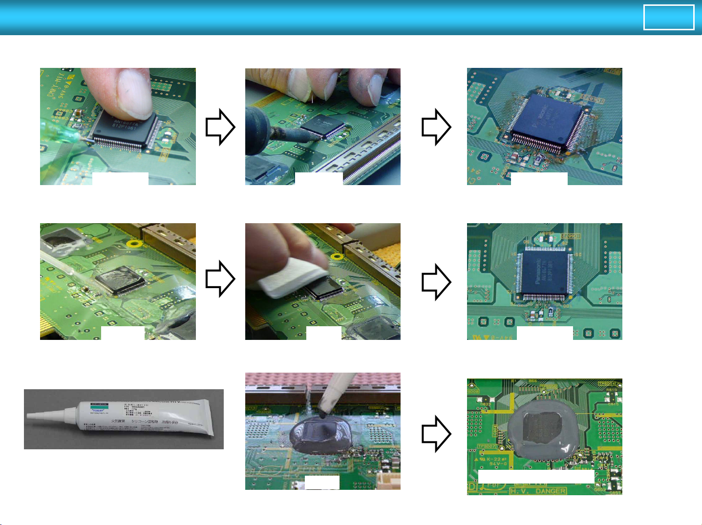
How to replacement of PDP Scan Driver IC on SN board
How to replacement of PDP Scan Driver IC on SN board
5. Installation of IC
2/2
6. Cleaning
7. Spreading of silicon glue
Silicone glue
Incase of Local procurement
*Product name:
http://www.dowcorning.com
(Part No.: T8CJ011)
DOW CORNING(R) SE9189L GRAY RTV
Soldering
spread
CompletionPositioning
CompletionWashing Wiping
Thicken time : 10 minute
The installation complete
Page 21
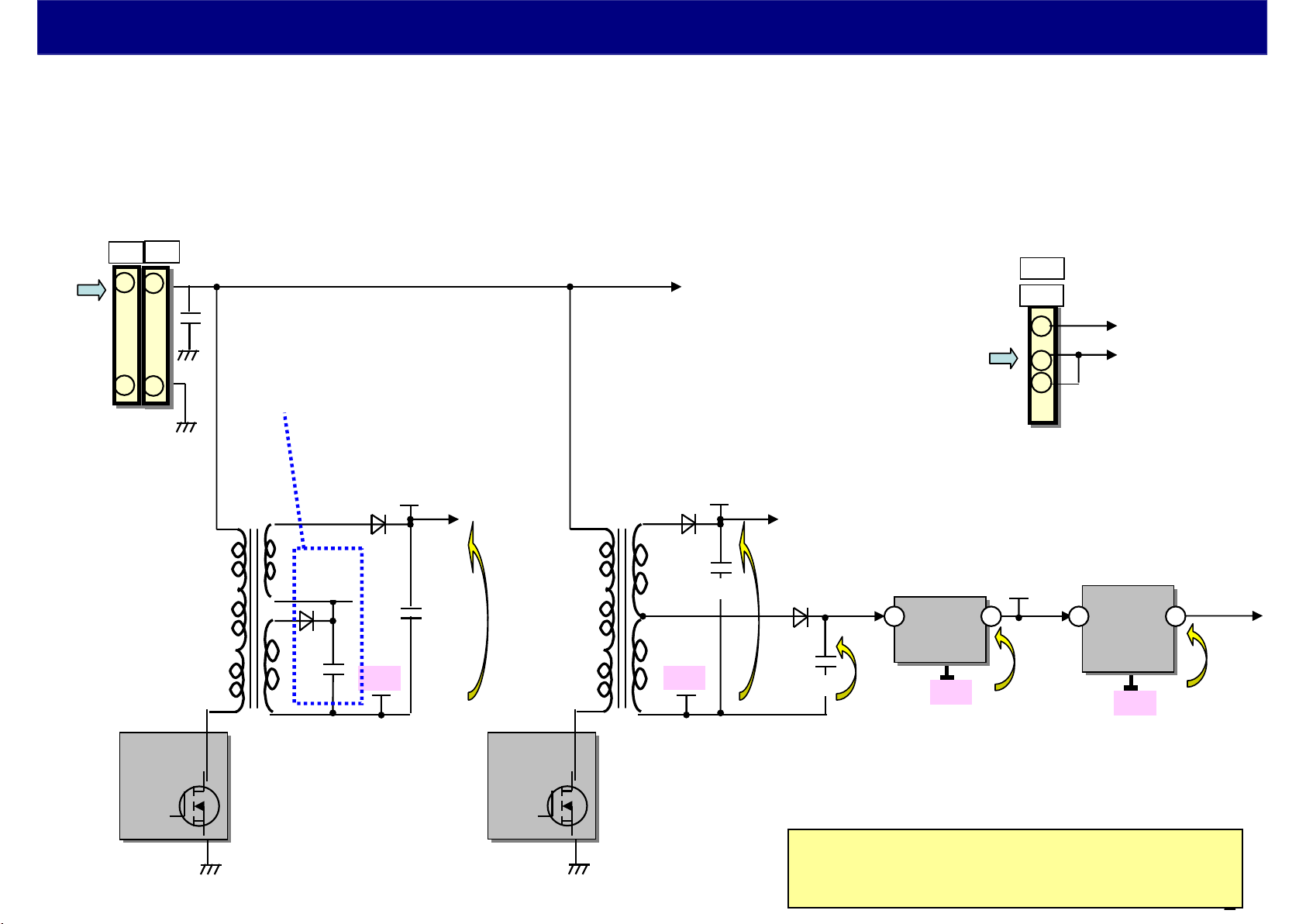
Block Diagram of Power Supply Circuit
All power supply circuit start automatically, when Vsus is input.
Vad, Vscn, F15V, and 5V_F are regulated from VFG.
So when you check the voltage, please confirm that basis is VFG.
SN2
SC2
Vsus(205V)
C16411
-415
Full-HD model only
P board
1
6
+
3
1
A board
< 2012 model >
SN20
SC20
30
1
2
P5V
P15V
T16471
DC/DC
DC/DC
IC16784
IC16784
GND
Vad2
+
D16712
D16711
(60V)
VFG
Vad
+
(200V)
C16813
T16472
DC/DC
DC/DC
IC16786
IC16786
GND
D16713
-714
C16842
VFG
Vscn (TPSC1)
(147V)
+
D16728
C16793
The value is one example of 50ST50 product.
(Vad / Vscn are different by each model)
Please check the accurate value by Service Manual.
+
(F20V)
(18V)
Regulator
Regulator
IC16795
IC16795
VFG
F15V
(14.6V)
Regulator
Regulator
/
/
Detection
Detection
IC16725
IC16725
VFG
F5V
22513
(5V)
21
Page 22
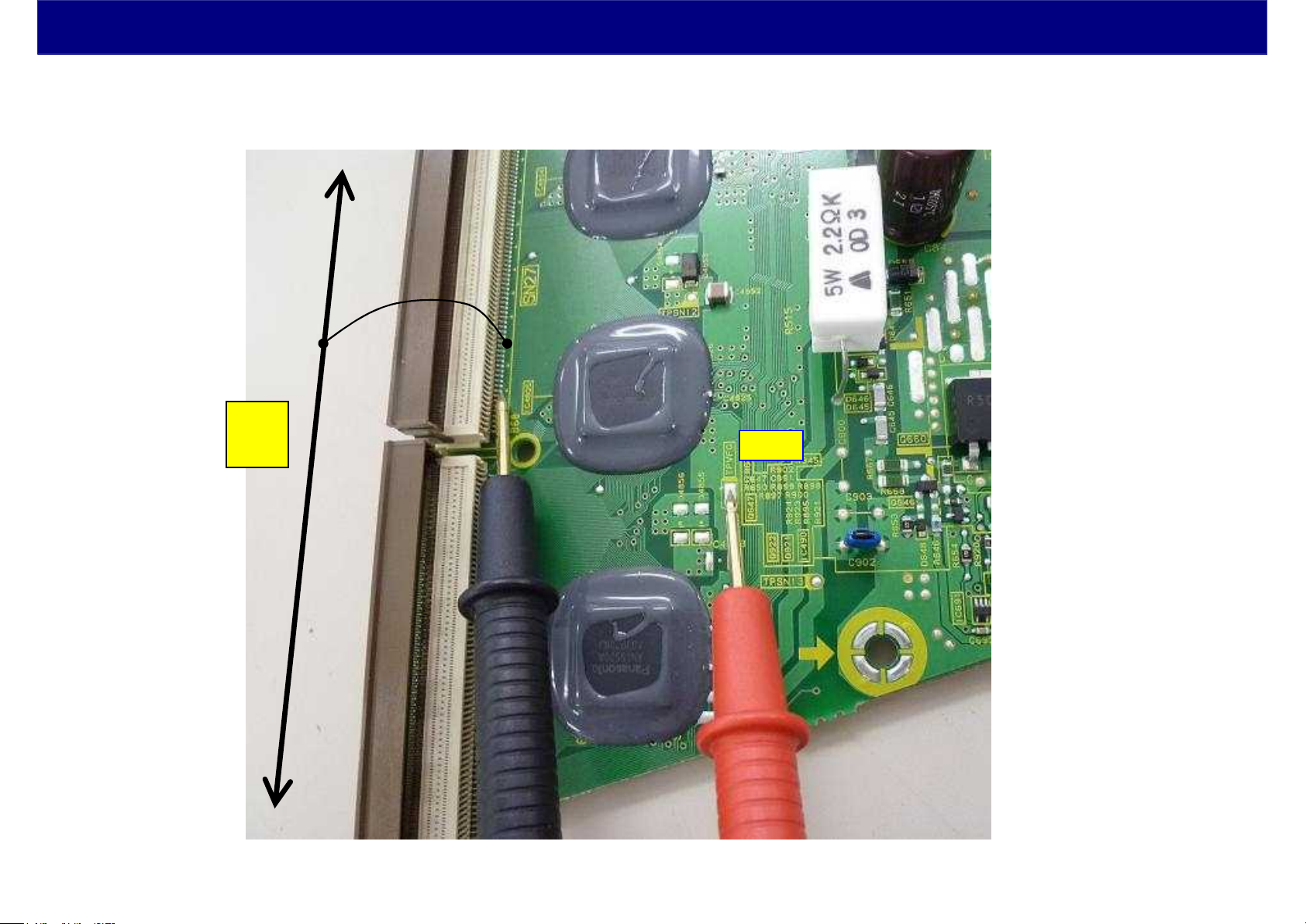
Block3. Short Circuit Check of Power Line and Check the Output Voltage
Check the short circuit of power line. If it is not short circuited,
then check the output voltage with the unit just before shutdown.
The block diagram of power supply circuit is described to the next page.
Symptom
(just for reference)
Except 6,7 blinks
Except 6,7 blinks
7 blinks
7 blinks
Output voltage / Check parts
Vsus : input from P board
(C16411 – 16415, 16507) ,
(R16503, 536, 537,605,618, 902,
D16536, C16502, 505, 531, 891 )
( IC16784(*2) or D16833, T16471,
IC16785, PC16897 )
Vscn , 16V_F
Basis of output voltage (*3)
From GND
from VFGVad
from VFG
Output voltage value
(*1: Depend on the model)
213V/210V/189V from GND
15.6V from GND From GNDP15V : input from P board
205V/200V/195V from VFG
147V from VFG (*3)
< 2012 model >
(*3)
( IC16786(*2) or D16720, T16472,
IC16787, PC16723 )
7 blinks
7 blinks
(*1) This value is different by each model.
So please check the accurate value by
the Service Manual.
(*2) The check of these components is not only
short circuit check also diode check.
Refer to the later page.
15V_F
( IC16795(*2) )
( IC16725(*2) )
from VFG
from VFG5V_F
(*3) Be careful
The basis is not GND.
If you check by oscilloscope,
don’t plug in the ground pin (3rdpin)
of the oscilloscope.
Isolate it from the earth of AC inlet.
18V from VFG (*3)
14.6V from VFG (*3)
5V from VFG (*3)
( This picture is a Japanese type )
Ground pin
(3rdpin)
22
Page 23
Other Block. Check the SOS Circuit-1 ( 2012 Full HD)
Monitor MID
< 2012 model >
If this voltage is out of range,
PC16581 is change to off.
SN20
SC20
28
A baord
SOS6
(Normal = Low)
If this signal is high(5V),
Normal = on
PC16581
(Photo coupler)
Inverter
(IC16563)
8 9
(5V)
LED
P15V
47k
22k
56k
Q16581
(Low V= stop)
Normal
D16582
(33V)
10k
D16581
(33V)
47k+47k
High V
37.4k
(=about half of Vsus)
ERR
ERM
L16411
-13
ERF
C16631
-632
Q16451
-452
GND
6blinks occurred.
The value is one example of 50ST50 product.
(Vscn / Vad and Zener diode are different by each model)
Please check the accurate value by Service Manual.
23
Page 24
Other Block. Check the SOS Circuit-2
< 2012 model >
Monitor 15V_F / 5V_F
SN20
4
Buffer
(IC
16563)
3
2
SC20
25
SOS7
A baord
(IC16561)
Switching signal for Scan output
Vdd (DC/DC of Vad)
Vdd (DC/DC of Vscn)
Hi = SOS
Low = enable
19
Buffer
Normal = on
(6V)
(6V)
P5V
Buffer
(IC
16563)
1
main_stop0
(Normal = Low)
PC16480
(Photo coupler)
Vad
F5V
560
1k
18
K
IC16471
Shunt
REG
A
VFG
VFG
If (F18V) rises than 25.2V from VFG
or F5V drops below 3.5V from VFG
or CHA line cuts,
FET of 18 pin switch off.
Then photo coupler changed to off, and
main_stop0 signal changed to high.
IC16725
(F18V)
D16791
(24V)
D16475
(5.1V)
1k
10k
VFG
(Normal = High)
REF
(F18V)
7
VFG
Vscn
20k
Q16471
7
2.2k
VFG
Vad
D16473
59k
F15V
5.6k
VFG
CHA
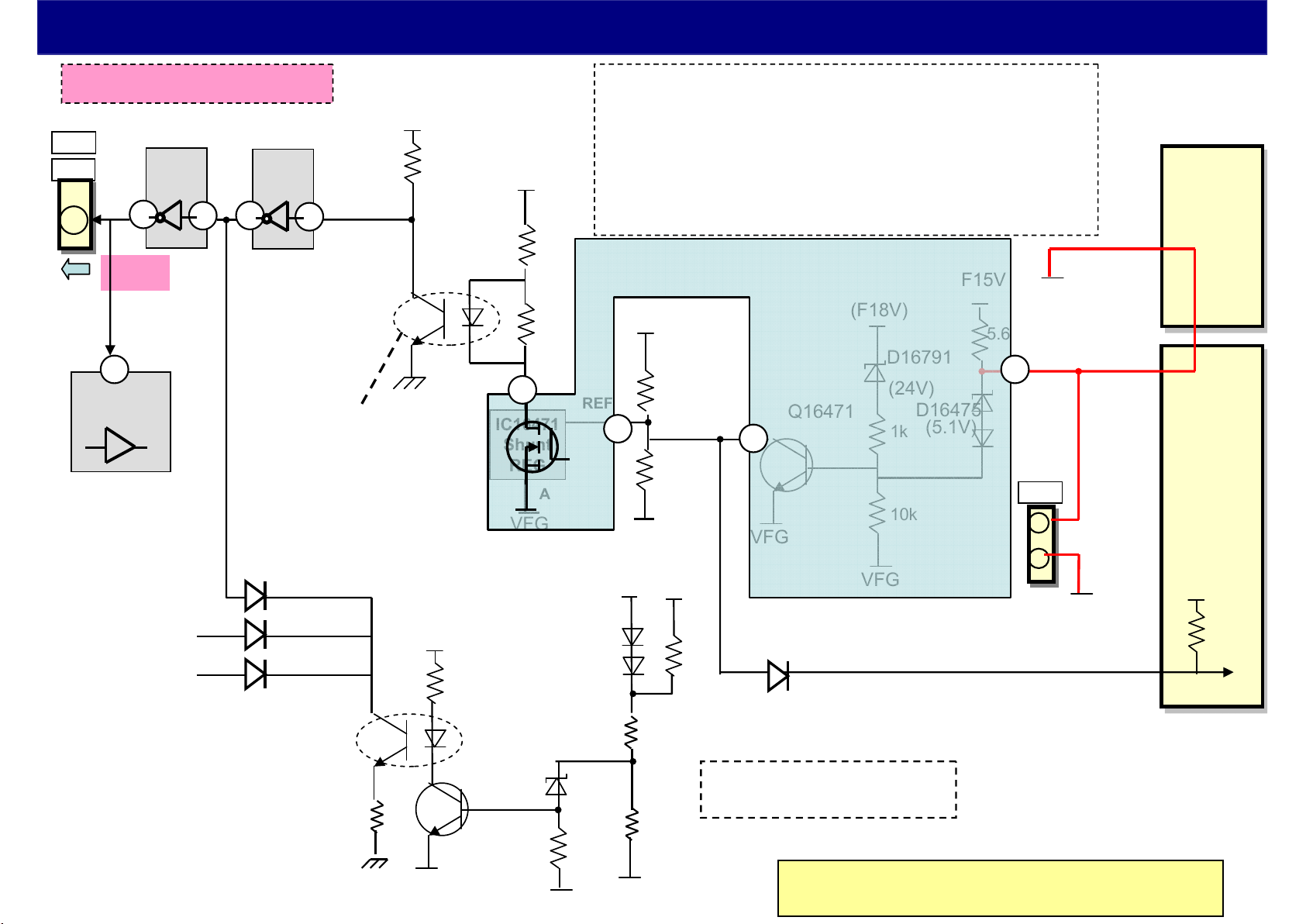
20
SC50
2
1
SCNR_PRO
VFG
SU
SU
Board
Board
SD
SD
board
board
5V_F
PC16896
VFG
(Vz=33V)
Q16815
VFG
10k
VFG
82k+61.9k
If Vscn or Vad rises,
Transistor Q16815 is ON.
37.4k
The value is one example of 50ST50 product.
Please check the accurate value by Service Manual.
24
Page 25
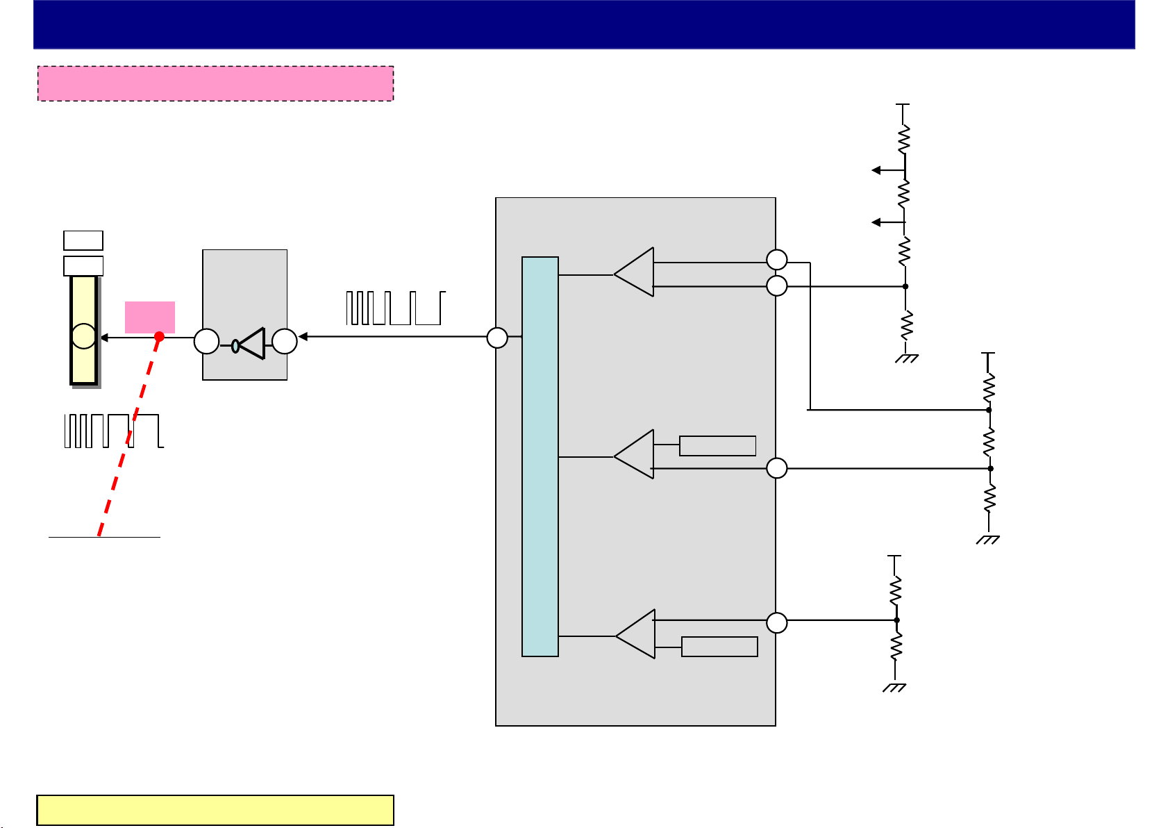
Other Block. Check the Feedback Circuit
< 2012 model >
Monitor VOL ( feed back to control IC)
SN20
SC20
Inverter
(IC16563)
UHZ
22
6 5
LO
12
L
O
G
I
Comparator
(IC16921)
+
-
+
-
REF 1.2V
P15V
22.6k
VTH2
1.47k
VTH1
8
7
976
VTH3
5.23k
Vad
69.8k+82.5k+82.5k
RAMP1
9
=234.8k
3.09k
RAMP2
7.87k
This signal is Feedback
signal to discharge control
IC on A board.
(If no feed back,
8 time blinks)
The value is one example of 50ST50 product.
C
VOL
120k+120k+120k
+
-
REF 2.5V
10
RAMP3
=360k
5.11k
25
Page 26
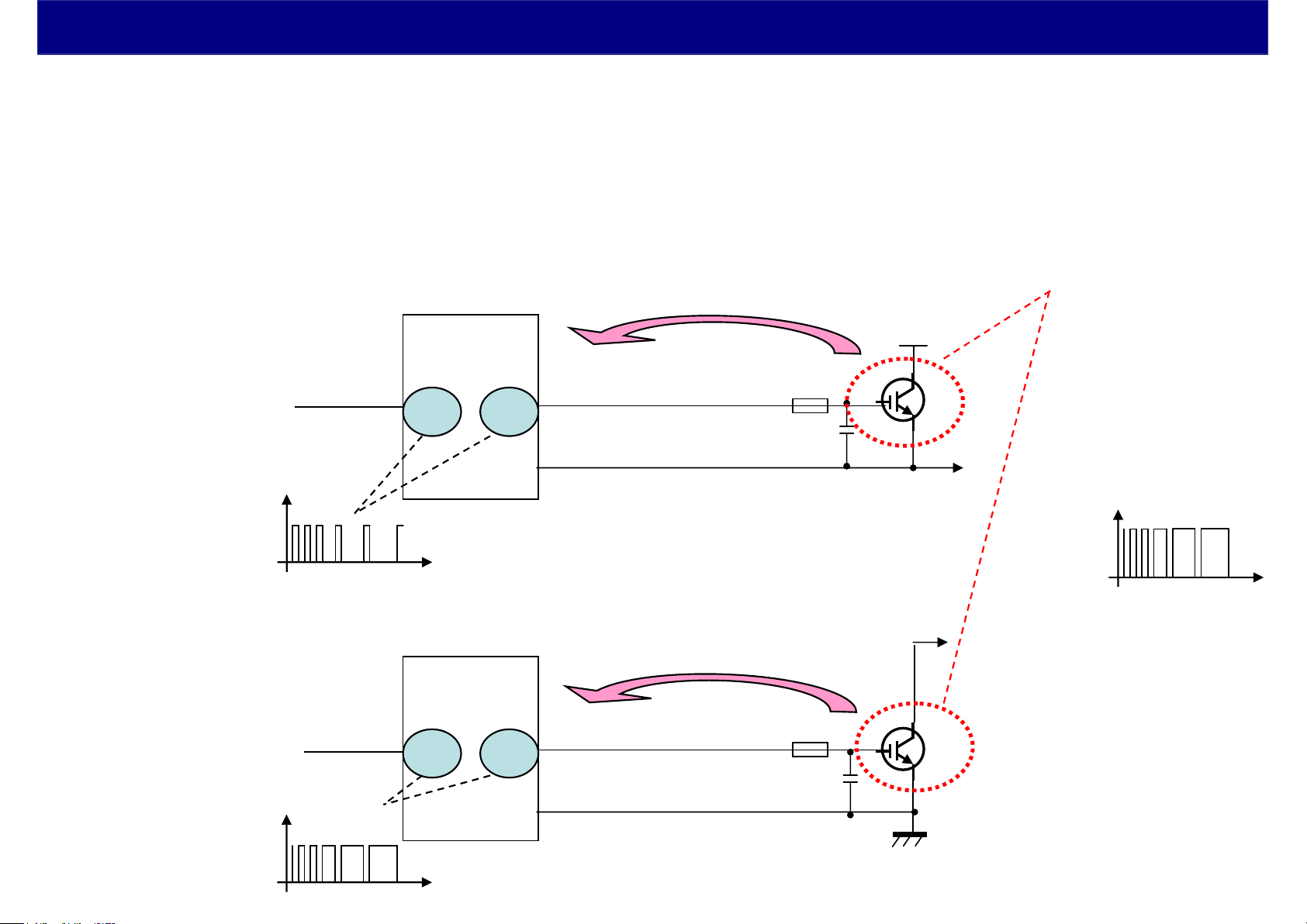
Supplement ( flow of control signal for scan pulse switching )
Scan pulse output waveform is produced by the many switching.
< 2012 model >
GND
IGBT
Driver3
(IC16524)
CSL
IGBT
Driver1
(IC16503)
CMH
L16411-12
C16631
-632
Q16451
-452
Q16401
FET
Driver1
(IC16600)
CPH1,CSH
IGBT
Driver4
(IC16504)
CSH,nCPH1
- 403
Q16441
-443
IGBT
Driver2
(IC16523)
CML
Vsus
GND
VOL
Q16421
-423
Vsus
(Q16762)
CIS,CEL
Q16600
Q16621
-623
IGBT
Driver5
-601
IGBT
Driver6
(IC16921)
nCEL,
-
+
GND
Q16661
CELR
Vad
Vscn
+
Vscn
-
Vad2
Q16646,647,660
Vscn shifted
VF0
To
SU/SD
board
VFG
26
Page 27
< 2012 model >
)
PC16461
PC16462
PC16461
IC16523
IC16524
Q16820
PC16685
Q16646,647,660
SD board
SD board
SD board
IC16921
PC16685
Supplement ( flow of control signal for scan pulse switching
IC16561
Q16921(IC16921)
27
Page 28

< 2012 model >
2-2-1.Check List of HD model-SN Board
T*-P42X5/X50/C5/C50*, TC-P46X5* :TNPA5592**
T*-P50X5/X50/C5/C50* :TNPA5593**
Check all components of this list, then try to power on.
28
Page 29
Check List (1/2)
< HD model-SN board >
T*-P42X5/X50/C5/C50*, TC-P46X5* :TNPA5592**
T*-P50X5/X50/C5/C50* :TNPA5593**
< 2012 model >
( ### )notation: only 50inch model=TNPA5593**
BLOCK1
Reference No.
Q16401, Q16402, D16401, D16402, (D16403)
#:Because of parallel circuit, check one of 5.
Q16421, Q16422, D16421
#:Because of parallel circuit, check one of 3.
Q16621, Q16622, D16641, D16642, (D16643)
#:Because of parallel circuit, check one of 5.
Q16661, D16673, D16674
#:Because of parallel circuit, check one of 3.
Q16601, D16618, R16601
Q16441, D16481
#:Because of parallel circuit, check one of 2.
Q16451, D16461
#:Because of parallel circuit, check one of 2.
D16432, D16435, D16722, D16723, D16725
D16432
Check
(Drive Circuit)
IC16501, R16401, R16402
IC16521, R16421, R16422
Q16762, R16761, R16621, R16622,
R16681, R16682
D16668, R16661
IC16600, R16612
IC16502, C16531, R16441
IC16522, C16551, R16451
---
Check
If defective, check also drive circuit
Q##, D## C## : Short check, R## : Open check, IC## : Diode check (refer to later page)
29
Page 30
Check List (2/2)
< HD model-SN board >
T*-P42X5/X50/C5/C50*, TC-P46X5* :TNPA5592**
T*-P50X5/X50/C5/C50* :TNPA5593**
< 2012 model >
CheckReference No.
BLOCK2
BLOCK3
Q##, D##, C##, IC14### : Short check, R## : Open check, IC16### : Diode check (refer to later page)
Short check between VFG and VFO.
If shorted, then short check output of each scan drive IC,
IC14901, 14902, 14903, 14904, 14951, 14952, 14953, 14954
IC16784, D16833, C16833
IC16786, D16720, C16834
IC16795, C16793, C16796
IC16725, C16723, C16724, C16725
C16411, C16412
#:Because of parallel circuit, check one of 2.
30
Page 31

Components of Check List in Schematic Circuit Diagram ( 1/4 )
< TNPA5592 >
R16612
IC16600R16536
C16411
C16412
R16537
R16538
D16536
< 2012 model >
D16618
R16601
Q16601
R16619
D16620
D16722
D16725
IC16522
IC16501
C16502
D16432
R16401
R16402
Q16401
Q16402
D16401
D16402
D16435
D16723
D16481
Q16441
R16451
C16551
Q16451
D16461
IC16502
C16531
R16441
IC16521
R16421
R16422
D16421
Q16421
Q16422
31
Page 32

Components of Check List in Schematic Circuit Diagram ( 2/4 )
< TNPA5592 >
< 2012 model >
IC16784
R16761
Q16762
C16833
D16833
D16711
C16813
IC16786
C16834
D16720
IC16795
C16796
C16842
D16713
D16714
C16724
IC16725
C16723
C16725
R16621
R16622
R16681
R16682
IC16921
D16668
R16661
Q16661
D16673
D16674
Q16621
Q16622
D16641
D16642
32
Page 33

Components of Check List in Schematic Circuit Diagram ( 3/4 )
< TNPA5592 >
IC14901 IC14902
< 2012 model >
IC14951
IC14952
33
Page 34

Components of Check List in Schematic Circuit Diagram ( 4/4 )
< TNPA5592 >
< 2012 model >
IC14903
IC14953
IC14904
IC14954
34
Page 35

Components Location of Check List on Board
< TNPA5592 >
< 2012 model >
A Block B Block C Block
35
Page 36

Components Location of Check List on Board ( A Block )
< TNPA5592 >
< 2012 model >
IC16725, C16723
C16724, C16725
D16432, D16435
D16722, D16723
D16725
IC14952IC14953IC14954
Q16441,D16481 IC16502, C16531, R16441 D16461,Q16451 IC16522, C16551, R16451
The printing of the reference No. on the PCB is abbreviated of 16. (For example: the reference No. C16502 is printed as C502. )
36
Page 37

Components Location of Check List on Board ( B Block )
< 2012 model >
< TNPA5592 >
Q16421,Q16422
D16421
IC14951
Q16762, R16761
R16621,R16622
R16681,R16682
D16401,D16402
Q16401,Q16402
TPVFG
IC14904
Q16621,Q16622
D16641,D16642
D16618
IC16521, R16421, R16422
The printing of the reference No. on the PCB is abbreviated of 16. (For example: the reference No. C16502 is printed as C502. )
IC16501, C16502
R16401, R16402
IC16600, R16612 C16411,C16412
R16601
Q16601
37
Page 38

Components Location of Check List on Board ( C Block )
< TNPA5592 >
< 2012 model >
IC14903
Q16661, D16673, D16674
IC14902
IC16795,C16796
TPVFO
IC14901
D16668,R16661 IC16784,D16833,C16833 IC16786,D16720,C16834
The printing of the reference No. on the PCB is abbreviated of 16. (For example: the reference No. C16502 is printed as C502. )
38
Page 39

Components of Check List in Schematic Circuit Diagram ( 1/4 )
< 2012 model >
< TNPA5593 >
C16411
C16412
R16619
D16620
D16722
D16725
R16536
R16537
R16538
D16536
IC16501
C16502
D16432
D16403
IC16600
R16612
D16618
R16601
Q16601
R16401
R16402
Q16401
Q16402
D16401
D16402
D16435
IC16522
R16451
C16551
Q16451
D16461
IC16502
C16531
R16441
IC16521
R16421
R16422
D16723
D16481
Q16441
D16421
Q16421
Q16422
39
Page 40

Components of Check List in Schematic Circuit Diagram ( 2/4 )
< TNPA5593 >
< 2012 model >
IC16784
R16761
Q16762
C16833
D16833
D16711
C16813
D16668
R16661
IC16786
C16834
D16720
IC16795
C16796
C16842
D16713
D16714
C16724
IC16725
C16723
C16725
R16621
R16622
R16681
R16682
IC16921
Q16661
D16673
D16674
Q16621
Q16622
D16641
D16642
D16643
40
Page 41

Components of Check List in Schematic Circuit Diagram ( 3/4 )
< TNPA5593 >
IC14901
IC14902
< 2012 model >
IC14951
IC14952
41
Page 42

Components of Check List in Schematic Circuit Diagram ( 4/4 )
< TNPA5593 >
< 2012 model >
IC14903
IC14904
IC14953
IC14954
42
Page 43

Components Location of Check List on Board
< TNPA5593** >
< 2012 model >
A Block B Block C Block
43
Page 44

Components Location of Check List on Board ( A Block )
< TNPA5593** >
< 2012 model >
C16724, C16725
D16643IC16725, C16723
IC14952IC14953IC14954
Q16441,D16481 IC16502, C16531, R16441 D16461,Q16451 IC16522, C16551, R16451
The printing of the reference No. on the PCB is abbreviated of 16. (For example: the reference No. C16502 is printed as C502. )
44
Page 45

Components Location of Check List on Board ( B Block )
< TNPA5593** >
< 2012 model >
D16432, D16435
D16722, D16723
D16725
IC14951
Q16621,Q16622
D16641,D16642
IC14904
D16618
R16601
Q16601
Q16421,Q16422
D16421
The printing of the reference No. on the PCB is abbreviated of 16. (For example: the reference No. C16502 is printed as C502. )
IC16521, R16421, R16422 Q16762, R16761
R16621,R16622
R16681,R16682
IC16501, C16502
R16401, R16402
IC16600, R16612
45
Page 46

Components Location of Check List on Board ( C Block )
< TNPA5593** >
< 2012 model >
IC14903
Q16661, D16673, D16674
TPVFG
IC14902
IC16795,C16796
TPVFO
IC14901
C16411,C16412 D16668,R16661
The printing of the reference No. on the PCB is abbreviated of 16. (For example: the reference No. C16502 is printed as C502. )
IC16784,D16833,C16833 IC16786,D16720,C16834
46
Page 47

< 2012 model >
2-2-2.Check List of Full-HD model-SN Board
T*-P42GT50/ST50* :TNPA5523**
T*-P42UT50* :TNPA5620**
47
Page 48

Check List (1/2)
< Full HD model-SN board >
T*-P42GT50/ST50* :TNPA5523**
< 2012 model >
BLOCK1
T*-P42UT50* :TNPA5620**
Reference No.
(Q16401), Q16402, (Q16403),
(D16401), D16402, (D16403)
#:Because of parallel circuit, check one of 6.
Q16421, Q16422, D16421
#:Because of parallel circuit, check one of 3.
Q16621, Q16622, (Q16623),
D16641, (D16643), (D16644)
#:Because of parallel circuit, check one of 5.
Q16661, D16673, D16674
#:Because of parallel circuit, check one of 3.
Q16600, (Q16601),
Check
( ### )notation: different by boards
(Drive Circuit)
IC16501, C16502,
(R16401), R16402, (R16403)
IC16521, R16421, R16422
Q16762, R16621, R16622, (R16623),
R16681, R16682, (R16683), R16761
D16669, R16661
Q16648, Q16652, R16649Q16660, R16561, D16652
IC16600, R16605, R16612
Check
(D16608), D16618, R16601
Q16441, (Q16442), D16481, (D16482)
#:Because of parallel circuit, check one of 4.
Q16451, (Q16452), D16461, (D16462)
#:Because of parallel circuit, check one of 4.
(D16430), D16432, (D16434)
IC16502, C16531, R16441, (R16442)
IC16522, C16551, R16451, (R16452)
---
If defective, check also drive circuit
Q##, D## C## : Short check, R## : Open check, IC## : Diode check (refer to later page)
48
Page 49

Check List (2/2)
< Full HD model-SN board >
T*-P42GT50/ST50* :TNPA5523**
T*-P42UT50* :TNPA5620**
< 2012 model >
( ### )notation: different by boards
CheckReference No.
BLOCK2
BLOCK3
Q##, D##, C##, IC14### : Short check, R## : Open check, IC16### : Diode check (refer to later page)
Short check between VFG and VFO.
If shorted, then short check output of each scan drive IC,
IC14601, 14602, 14603, 14604, 14605, 14606,
IC14801, 14802, 14803, 14804, 14805, 14806
IC16784, D16833, C16833
IC16786, D16720, C16834
IC16795, C16793, C16796
IC16725, C16723, C16724
C16411, C16412, (C16413), (C16414)
#:Because of parallel circuit, check one of 4.
49
Page 50

Components of Check List in Schematic Circuit Diagram ( 1/5 )
< TNPA5523 >
< 2012 model >
C16411, C16412
C16413, C16414
R16536
R16537
D16536
IC16501
C16502, C16503
IC16502
C16531
D16432
IC16600
R16612
Q16600,R16603
D16618
R16601
Q16601
R16402
R16403
Q16402
Q16403
D16402
D16403
Q16441
Q16442
R16441
R16442
IC16522
C16551
D16430
R16451
Q16451
Q16452
D16461
D16462
IC16521
D16481
D16482
Q16421
Q16422
D16421
R16421
R16422
50
Page 51

Components of Check List in Schematic Circuit Diagram ( 2/5 )
< TNPA5523 >
< 2012 model >
IC16784
C16813
C16833
D16833
D16711
IC16786
C16834
D16720
IC16795
C16796
D16713
D16714
C16842
R16621, R16622
R16623, R16681
R16682, R16683
R16761
Q16762
IC16921
Q16621, Q16622
Q16623, D16641
D16644
Q16661
D16673
D16674
D16669, R16661
51
Page 52

Components of Check List in Schematic Circuit Diagram ( 3/5 )
< TNPA5523 >
IC16725
C16724
C16723
< 2012 model >
52
Page 53

Components of Check List in Schematic Circuit Diagram ( 4/5 )
< TNPA5523 >
< 2012 model >
IC14601
IC14602
IC14603
IC14801
IC14802
IC14803
53
Page 54

Components of Check List in Schematic Circuit Diagram ( 5/5 )
< TNPA5523 >
< 2012 model >
IC14604 IC14605
IC14606
IC14804
IC14805
IC14806
54
Page 55

Components Location of Check List on Board
< TNPA5523 >
< 2012 model >
A Block
B Block
C Block
55
Page 56

Components Location of Check List on Board ( A Block )
< TNPA5523 >
< 2012 model >
IC14806
IC16795,C16796
Q16661, D16673
D16674
TPSN1
(VFO)
IC14805
TPVFG
IC14804
IC14803 IC14802
IC16725
C16723
C16724
IC16786,D16720,C16834
IC16784,D16833,C16833
D16669, R16661
The printing of the reference No. on the PCB is abbreviated of 16. (For example: the reference No. C16502 is printed as C502. )
56
Page 57

Components Location of Check List on Board ( B Block )
< TNPA5523 >
< 2012 model >
Q16762, R16761
R16621, R16622
R16623, R16681
R16682, R16683
Q16421,Q16422
D16421
IC14801
IC14606 IC14605
IC14604
Q16621,Q16622
Q16623, D16641
D16644
Q16441, Q16442
D16481, D16482
IC16521, R16421
R16422
D16430, D16432
Q16600, R16603
C16503
IC16600, R16612
The printing of the reference No. on the PCB is abbreviated of 16. (For example: the reference No. C16502 is printed as C502. )
D16618
R16601
Q16601
IC16502, C16531
R16441, R16442
IC16522, C16551
57
Page 58

Components Location of Check List on Board ( C Block )
< TNPA5523 >
IC14602 IC14601
IC14603
Q16402,Q16403
D16402,Q16403
< 2012 model >
C16411,C16412
C16413, C16414
IC16501, C16502
R16402, R16403
R16451
The printing of the reference No. on the PCB is abbreviated of 16. (For example: the reference No. C16502 is printed as C502. )
Q16451, Q16452
D16461, D16462
58
Page 59

Components of Check List in Schematic Circuit Diagram ( 1/5 )
< TNPA5620 >
< 2012 model >
IC16502
C16531
C16411, C16412
R16536
R16537
D16536
IC16501
C16502, C16503
IC16600
R16612
D16618
R16601
Q16601
R16401
R16402
Q16401
Q16402
D16401
D16402
R16441
IC16522
D16432
C16551 R16451 Q16451
D16461
D16434
IC16521
Q16441
D16481
Q16421
Q16422
D16421
R16421
R16422
59
Page 60

Components of Check List in Schematic Circuit Diagram ( 2/5 )
< TNPA5620 >
C16834
D16711C16813 IC16786
C16833
D16833
IC16784
D16720
< 2012 model >
IC16795
C16796
D16713
D16714
C16842
Q16762
R16621
R16622
R16681
R16682
IC16921
Q16621
Q16622
D16641
D16643
Q16661
D16673
D16674
D16669, R16661
60
Page 61

Components of Check List in Schematic Circuit Diagram ( 3/5 )
< TNPA5620 >
C16723
C16724
IC16725
< 2012 model >
61
Page 62

Components of Check List in Schematic Circuit Diagram ( 4/5 )
< TNPA5620 >
< 2012 model >
IC14601
IC14602
IC14603
IC14801
IC14802
IC14803
62
Page 63

Components of Check List in Schematic Circuit Diagram ( 5/5 )
< TNPA5620 >
< 2012 model >
IC14604 IC14605
IC14606
IC14804
IC14805
IC14806
63
Page 64

Components Location of Check List on Board
< TNPA5620 >
< 2012 model >
A Block
B Block
C Block
64
Page 65

Components Location of Check List on Board ( A Block )
< TNPA5620 >
< 2012 model >
IC14806 IC14805
Q16661, D16673
D16674
TPVFG
IC14804 IC14803 IC14802
TPVFO
D16713, D16714
C16842
D16711,C16813
D16669, R16661
IC16784,D16833,C16833
The printing of the reference No. on the PCB is abbreviated of 16. (For example: the reference No. C16502 is printed as C502. )
IC16795,C16796
IC16786
D16720,C16834
65
Page 66

Components Location of Check List on Board ( B Block )
< TNPA5620 >
IC14606 IC14605 IC14604
Q16762
IC14801
R16621, R16622
R16681, R16682
< 2012 model >
Q16451, D16461
IC16725
C16723
C16724
Q16421,Q16422
D16421
The printing of the reference No. on the PCB is abbreviated of 16. (For example: the reference No. C16502 is printed as C502. )
IC16521, R16421
R16422
IC16522
C16551, R16451
Q16621,Q16622
D16641,D16643
D16432, D16434
66
Page 67

Components Location of Check List on Board ( C Block )
< TNPA5620 >
IC14602
IC14603
< 2012 model >
IC14601
Q16601
Q16441, D16481
IC16502
C16531,R16441
D16536
R16536
R16537
The printing of the reference No. on the PCB is abbreviated of 16. (For example: the reference No. C16502 is printed as C502. )
D16618,R16601
IC16600, R16612
IC16501
C16502, C16503
R16402, R16403
Q16401,Q16402
D16401,Q16402
C16411,C16412
67
Page 68

< 2012 model >
2-2-3.Check List of Full-HD model-SC Board
T*-P50/55 VT50/GT50/ST50* :TNPA5528**
T*-P50/55 UT50/U50 :TNPA5621**
T*-P60/65 VT50/GT50/ST50* :TNPA5647**
T*-P60UT50* :TNPA5538**
68
Page 69

Check List (1/2)
< Full HD model-SC board >
T*-P50/55 VT50/GT50/ST50* :TNPA5528**
T*-P50/55 UT50/U50 :TNPA5621**
T*-P60/65 VT50/GT50/ST50* :TNPA5647**
T*-P60UT50* :TNPA5538**
< 2012 model >
( ### )notation: different by boards
BLOCK1
Reference No.
(Q16401), (Q16402), (Q16403), (Q16404),
(D16401), (D16402), (D16403), (D16404)
#:Because of parallel circuit, check one of 4-6.
(Q16421), (Q16422), (Q16423), (Q16424),
(D16421), (D16422), (D16423), (D16424)
#:Because of parallel circuit, check one of 3-5.
(Q16621), Q16622, (Q16623), (Q16624), (Q16625)
D16641, D16642, D16643, (D16644)
#:Because of parallel circuit, check one of 4-8.
Q16661, D16673, D16674
#:Because of parallel circuit, check one of 3.
(Q16600), Q16601, (D16608), D16618, R16601
(Q16441), (Q16442), (Q16443),
Check
(Drive Circuit)
IC16503, C16502,
(R16401), (R16402), (R16403), (R16404)
IC16523,
(R16421), R16422, (R16423), (R16424)
Q16762, (R16621), (R16622), (R16623),
(R16624), (R16625), (R16681), (R16682),
(R16683), (R16684), (R16687), R16761
D16669, R16661
Q16648, Q16652, R16649Q16660, R16651, D16652
IC16600, (R16605), R16612
IC16504, C16531,
Check
(D16481), (D16482), (D16483)
#:Because of parallel circuit, check one of 6.
(Q16451), (Q16452), (Q16453),
(D16461), (D16462), (D16463)
#:Because of parallel circuit, check one of 6.
D16430, D16432
Q##, D## C## : Short check, R## : Open check, IC## : Diode check (refer to later page)
(R16441), (R16442), (R16443)
IC16524, C16551,
(R16451), (R16452), (R16453)
---
If defective, check also drive circuit
69
Page 70

Check List (2/2)
< Full HD model-SC board >
T*-P50/55 VT50/GT50/ST50* :TNPA5528**
T*-P50/55 UT50/U50 :TNPA5621**
T*-P60/65 VT50/GT50/ST50* :TNPA5647**
T*-P60UT50* :TNPA5538**
< 2012 model >
( ### )notation: different by boards
CheckReference No.
BLOCK3
Q##, D##, C## : Short check, R## : Open check, IC16### : Diode check (refer to later page)
IC16784, D16833, C16833
IC16786, D16720, C16834
IC16795, C16793, C16796
IC16725, C16723, C16724
C16411,
(C16412, C16413, C16414, C16415, C16416, C16417, C16418, C16419, C16420)
#:Because of parallel circuit, check one of them.
70
Page 71

Components of Check List in Schematic Circuit Diagram ( 1/3 )
< TNPA5528 >
D16618
C16411, C16412
C16413, C16414
Q16601
R16601
Q16600
< 2012 model >
D16608
Q16401
Q16402
Q16403
D16401
D16402
D16404
Q16451
Q16452
D16461
D16462
Q16441,Q16442
D16481,D16482
Q16422
Q16423
Q16424
D16421
D16432 D16430
71
Page 72

Components of Check List in Schematic Circuit Diagram ( 2/3 )
< TNPA5528 >
C16834
IC16786
C16833
D16833
IC16784
D16720
< 2012 model >
IC16795
C16793
C16796
Q16621,Q16622
Q16623,Q16624
D16641,D16642
D16643,D16644
Q16660
R16651
D16652
Q16661
D16673
D16674
72
Page 73

Components of Check List in Schematic Circuit Diagram ( 3/3 )
< TNPA5528 >
< 2012 model >
C16724
IC16725
73
Page 74

Components Location of Check List on Board
< TNPA5528 >
Q16621,Q16622
Q16623,Q16624
D16641,D16642
D16643,D16644
Q16661
D16673
D16674
IC16795
C16793
C16796
IC16786
C16834
D16720
Q16422
Q16423
Q16424
D16421
Q16401
Q16402
Q16403
D16401
D16402
D16404
< 2012 model >
C16411
C16412
C16413
C16414
VFG
TPSC1
(VFO)
VFG
VFG
VFG
Q16601
Q16660
R16651
D16652
The printing of the reference No. on the PCB is abbreviated of 16. (For example: the reference No. C16502 is printed as C502. )
IC16784
D16833
C16833
IC16725
C16724
R16601
Q16600
D16618
D16608
Q16441
Q16442
D16481
D16482
D16430
D16432
Q16451
Q16452
D16461
D16462
74
Page 75

Components of Check List in Schematic Circuit Diagram ( 1/2 )
< TNPA5621 >
Q16601
C16411, C16412
R16601
D16618
< 2012 model >
Q16401
Q16402
D16402
D16403
Q16451
D16461
Q16441,D16481
Q16421
Q16422
D16421
D16432 D16430
75
Page 76

Components of Check List in Schematic Circuit Diagram ( 2/2 )
< 2012 model >
< TNPA5621 >
IC16784
C16833
D16833
IC16786
C16834
D16720
IC16795
C16793
C16796
C16724
IC16725
Q16622,Q16623
D16641,D16643
Q16661
D16673
D16674
Q16660
R16651
D16652
76
Page 77

Components Location of Check List on Board
< TNPA5621 >
Q16661
D16673
D16674
IC16795
C16793
C16796
IC16786
C16834
D16720
IC16725
C16724
TPSC1
(VFO)
Q16622,Q16623
D16641,D16643
< 2012 model >
Q16401
Q16402
D16402
D16403
VFGVFGVFGVFG
Q16660
R16651
D16652
The printing of the reference No. on the PCB is abbreviated of 16. (For example: the reference No. C16502 is printed as C502. )
IC16784
D16833
C16833
Q16421
Q16422
D16421
Q16451
D16461
D16430
D16432
Q16441
D16481
Q16601
R16601
D16618
C16411
C16412
77
Page 78

Components of Check List in Schematic Circuit Diagram ( 1/3 )
< TNPA5647 >
D16618
C16411, C16412
C16413, C16414
C16416
Q16601
R16601
Q16600
< 2012 model >
D16608
Q16401
Q16402
Q16403
Q16404
D16401
D16402
D16403
D16404
D16432
Q16451
Q16452
Q16453
D16462
D16463
Q16421
Q16422
Q16423
Q16441,Q16443
D16482,D16483
D16430
D16421
D16422
78
Page 79

Components of Check List in Schematic Circuit Diagram ( 2/3 )
< TNPA5647 >
C16834
C16833
D16833
IC16784
IC16786
D16720
IC16795
< 2012 model >
C16793
C16796
Q16660
R16651
D16652
Q16621,Q16622
Q16624,Q16625
D16641,D16642
D16643,D16644
Q16661
D16673
D16674
79
Page 80

Components of Check List in Schematic Circuit Diagram ( 3/3 )
< TNPA5647 >
< 2012 model >
C16724
IC16725
80
Page 81

Components Location of Check List on Board
< TNPA5647 >
< 2012 model >
Q16661
D16673
D16674
IC16795
C16793
C16796
TPSC1
(VFO)
IC16786
C16834
D16720
Q16421
Q16422
Q16423
D16421
D16422
Q16621,Q16622
Q16624,Q16625
D16641,D16642
D16643,D16644
VFGVFGVFG
Q16401,Q16402
Q16403,Q16404
D16401,D16402
D16404,D16404
VFG
C16411
C16412
C16413
C16414
C16416
Q16601
Q16660
R16651
D16652
The printing of the reference No. on the PCB is abbreviated of 16. (For example: the reference No. C16502 is printed as C502. )
IC16784
D16833
C16833
IC16725
C16724
R16601
Q16600
D16618
D16608
Q16441
Q16443
D16482
D16483
D16430
D16432
Q16451
Q16452
Q16453
D16462
D16463
81
Page 82

Components of Check List in Schematic Circuit Diagram ( 1/3 )
< TNPA5538 >
< 2012 model >
C16416, C16417
C16418, C16419
D16432
Q16601
R16601
D16618
Q16403
Q16404
D16401
D16402
D16403
Q16442,D16482
D16462
Q16422
Q16423
D16421
D16422
D16430Q16452
82
Page 83

Components of Check List in Schematic Circuit Diagram ( 2/3 )
< TNPA5538 >
C16834
IC16786
C16833
D16833
IC16784
D16720
< 2012 model >
IC16795
C16793
C16796
Q16621
Q16622
Q16624
D16642
D16644
Q16660
R16651
D16652
Q16661
D16673
D16674
83
Page 84

Components of Check List in Schematic Circuit Diagram ( 3/3 )
< TNPA5538 >
< 2012 model >
C16724
IC16725
84
Page 85

Components Location of Check List on Board
< TNPA5538 >
< 2012 model >
Q16661
D16673
D16674
IC16795
C16793
C16796
TPSC1
(VFO)
IC16786
C16834
D16720
IC16725
C16724
Q16621
Q16622
Q16624
D16642
D16644
VFGVFGVFG
VFG
Q16403
Q16404
D16401
D16402
D16403
Q16660
R16651
D16652
The printing of the reference No. on the PCB is abbreviated of 16. (For example: the reference No. C16502 is printed as C502. )
IC16784
D16833
C16833
Q16422
Q16423
D16421
D16422
Q16452
D16462
D16430
D16432
Q16442
D16482
Q16601
R16601
D16618
C16416
C16417
C16418
C16419
85
Page 86

< 2012 model >
2-3. Repair Data
86
Page 87

Defective case study
a. HD model-SN board (TNPA5592** / TNPA5593**)
< 2012 model >
BLOCK1 only
BLOCK1 (+Drive)
BLOCK2 only
Reference No.
Q16621,16622
IC16502, R16503, PC16462
IC16784, IC16786
T16472, IC16786
C16412
Number of case
1
1Q16661, R16661
1Q16401,16402, Q16421,16422, R16422
1Q16401,16402, Q16421,16422,
8One of IC14901,14902,14903,14904,14951,14952,14953,14954
1BLOCK3 only
1
1
(IC16784,IC16786) 1Q16621,16622, Q16661BLOCK1+BLOCK3
#: ”Drive” means drive circuit of IGBT/FET (connect to the base/gate of IGBT/FET).
87
Page 88

Defective case study
< 2012 model >
c. Full-HD model-SC board (TNPA5528** / TNPA5621** / TNPA5647** / TNPA5538**)
Number of caseReference No.
2Q16621, Q16661BLOCK1 only
1IC16786Q16402,16403, Q16422,16424, D16421BLOCK1 + BLOCK3
1(IC16784,IC16786)Q16621,16622, Q16661
88
Page 89

< 2011 model >
3-1.Explanation of Scan Board Operation
and Check Point
89
Page 90

Check Flow of SC/SN Board Repair
< 2011 model >
Before power-on for checking, replace all defective components in BLOCK 1, 2 and 3.
Block1.
Check of IGBT/Tr (C-E),
FET (S-D) and Diode
All OK
Block2.
Check of Scan Drive IC
(Only SN board)
All OK
Block3.
Check of power circuit
Shorted
Shorted
Shorted
Block1
Check also control
signal drive circuit
All OK
Shorted
Replace the defective
components
Replace the defective
components
Replace the defective
components
All OK
Power on check
After replacing all defective component,
Check with power. (especially HD model)
NG
Other Block. Check the SOS circuit and feed back circuit
Check the control signals
( Photo Coupler )
90
Page 91

Block Diagram of Scan Pulse Drive
< 2011 model >
Scan pulse output waveform is produced by switching of Vsus/Vad/GND.
( Energy recovery circuit )
C16631-
632
SN board of HD model
(X3/X30/C3/C30 series)
SN3
L16441
Q16451
-452
GND
Q16401
- 403
Q16441
D16481D16461
-443
Vsus
GND
Vsus
VOL
Q16421
-423
Vscn shifted
Q16600
-601
Q16621
-623
Vscn
VF0
Q16660
+
Vscn
-
VFG
Vad
+
Q16661
GND
< VFG waveform (VFO is added Vscn voltage to VFG) >
Vsus
.
.
.
Only SN board
(SC board is
separated to
SU/SD board)
To
SS
board
Q16451
L16441
Q16441
GND
Vad
(Vscn)
91
Page 92

BLOCK1. Short Circuit Check of the Switching Component and Diode
< 2011 model >
Check the short circuit “all” of the below switching components.
( just check short or not )
In many cases, there are several defective components at the same time.
Check components ( Defective components )
:FET(D-S) , Transistor (C-E) , Diode (K-A)
Q16401 - 404 / D16401 - 402
Q16421 - 424 / D16421 - 422
Q16621 - 624 / D16641 - 644
Q16661 / D16673 - 674
Q16660 / D16652 Full HD Only
Q16600 - 601 / D16618, R16601 ( open check)
Q16441 - 443 / D16481 - 483
Q16451 - 453 / D16461 - 462
D16430 - 434, D16722, D16723
(D16725), (D16726)
The Scan board is producing the scan pulse output (VFO and VFG) by switching of
several kinds of voltage. ( refer to the next page )
In main case of the defect, these switching components are short-circuited.
92
Page 93

BLOCK1 Drive Circuit ( Switching Control Signal 1 )
If drive IC is defect (=always output switch-on signal), the switching component
must be damaged. Check also the drive circuit when the switching component is defect.
< 2011 model >
< example: IC16501,16521 >
IC16501
Buffer (Drive IC)
VDD
IN OUT
VS
VOL+15V
VOL
IC16521
Buffer (Drive IC)
C
Q16501
R
R
R
15V
15V
If these switching
components are defect,
check also Drive
components.
Vsus
Q16401/402
R
VOL
Vsus
VOL
GND
VOL
15V
GND
VDD
IN OUT
VS
C
Q16521
R
Q16421/422
R
93
Page 94

BLOCK1 Drive Circuit ( Switching Control Signal 2 )
Drive Circuit (Switching Control Signal)Check components ( Defective components )
:FET(D-S) , Transistor (C-E) , Diode (K-A)
IC16501, C16502, Q16501, R16401-402, R16503Q16401 – 404 / ( D16401-402)
IC16521, R16525, Q16521, R16421-423, R16506Q16421 – 424 / ( D16421-422 )
Q16762, R16621-622, R16681-682Q16621 – 624 / ( D16641-644 )
D16669, R16661Q16661 / ( D16673 - 674 )
Q16647, R16649Q16660 / ( D16652)
Q16606, R16612Q16600 -601 , D16618, R16601 ( open check)
IC16502, C16531, Q16531, R16441, R16531Q16441 – 443 / ( D16481-483 )
IC16522, C16551, Q16551, R16451Q16451 – 453 / ( D16461-462 )
< 2011 model >
If defective, check also drive circuit
94
Page 95

How to check the Drive ICs and Power IC
We can check the power IC and drive IC by DIODE CHECK.
The check terminal is as below.
Diode check ( Check pin : Normal voltage )
< 2011 model >
BLOCK1
BLOCK3
(Explanation
is as later
page)
# Check after
replacing the
defective
components of
BLOCK1 and 2.
IC16501, IC16502, IC16521, IC16522,
IC16684
(Drive signal for switching
components)
IC16784, IC16786
(power IC)
IC16795, 16724
(power IC)
Don’t mistake the polarity.
3pin (+) and 1 pin(-) : 0.55V +/- 0.2V
3pin (+) and 2 pin(-) : 0.55V +/- 0.2V
3pin (+) and 7 pin(-) : 0.6V +/- 0.2V
2pin (+) and 1 pin(-) : 0.75V +/- 0.2V
7pin (+) and 1 pin(-) : 0.6V +/- 0.2V
8pin (+) and 1 pin(-) : 0.5V +/- 0.2V
8pin (+) and 3 pin(-) : 0.7V +/- 0.2V
8pin (+) and 4 pin(-) : 0.7V +/- 0.2V
8pin (+) and 5 pin(-) : 0.5V +/- 0.2V
2pin (+) and 1pin(-) : 0.55V +/- 0.2V
2pin (+) and 3 pin(-) : 0.5V +/- 0.2V
1pin (+) and 3pin(-) : 0.65V +/- 0.2V
Diode check
i
example
0.6V
+ -
95
Page 96

BLOCK2. Short circuit check of Scan Drive IC (Only SN Board)
< 2011 model >
Check the short circuit between VFG and VFO. If shorted, some of the Scan Drive IC is
defective. You can find the defective IC by checking the short circuit between VFG and
all output pin of Scan Drive IC (same as all pin of Connector SN11-18/21-28).
IC14901
Scan
Drive
IC
Scan
Drive
IC
IC14902
IC14953
Scan
Drive
IC
Scan
Drive
IC
IC14954
Scan Drive IC
Only SN board
(SC board is
separated to
SU/SD board)
( Energy recovery circuit )
C16631-
L16441
632
Q16451
-452
GND
SN board of HD model
(X3/X30/C3/C30 series)
SN3
Q16401
- 403
Q16441
-443
D16481D16461
Vsus
GND
Vsus
VOL
Q16421
-423
Q16600
-601
Q16621
-623
Vscn
Q16660
+
-
-
Vad
+
Q16661
GND
Check short circuit
(refer to the picture of
TPSC1/
TPSN1
VF0
Vscn
VFG
SN11/21
SN12/22
.
.
.
.
.
.
Output pin
SN17/27
SN18/28
Output pin
To
SS
board
Q16451
L16441
2012 explanation page)
Q16441
96
Page 97

Block Diagram of Power Supply Circuit
All power supply circuit start automatically, when Vsus is input.
Vad, Vscn, F15V, and 5V_F are regulated from VFG.
So when you check the voltage, please confirm that basis is VFG.
#: Check after replacing the defective components of BLOCK1 and 2.
< 2011 model >
P board
SC2
1
3
Vsus(205V)
T16471
D16711
VFG
Vad
+
C16813
(200V)
T16472
D1671314
C16842
VFG
Vscn
+
(147V)
D16728
+
C16793
(F18V)
(18V)
A board
Regulator
Regulator
IC16795
IC16795
VFG
SC20
35
6
7
F15V
(14.6V)
P5V
P15V
Regulator
Regulator
IC16724
IC16724
VFG
5V_F
(5V)
DC/DC
DC/DC
IC16784
IC16784
GND
DC/DC
DC/DC
IC16786
IC16786
GND
The value is one example of 46ST30 product.
(Vad / Vscn are different by each model)
Please check the accurate value by Service Manual.
97
Page 98

BLOCK3. Check of Power Circuit
How to check power IC is refer to the previous page.
If check the output voltage with the TV unit, be careful about the basis line.
< 2011 model >
Power line / Check components
Vsus : input from P board
(C16411 – 16414, 16507) ,
(R16525, 526, 536, 537,D16536,
C16502, 505, 531,551 )
( IC16784 or D16833, T16471,
IC16785, PC16897 )
Vscn , 16V_F
( IC16786 or D16720, T16472,
IC16787, PC16723 )
15V_F
( IC16795, C16793 )
Basis of output voltage (*2)
From GND
from VFGVad
from VFG
from VFG
Reference : output voltage value
(*1: Depend on the model)
215V/205V/189V from GND
15.6V from GND From GNDP15V : input from P board
205V/200V/195V from VFG (*2)
147V from VFG (*2)
18V from VFG (*2)
14.6V from VFG (*2)
( IC16724 )
(*1) This value is different by each model.
So please check the accurate value by
the Service Manual.
from VFG5V_F
(*2) Be careful
The basis is not GND.
If you check by oscilloscope,
don’t plug in the ground pin (3rdpin)
of the oscilloscope.
Isolate it from the earth of AC inlet.
5V from VFG (*2)
( This picture is a Japanese type )
Ground pin
(3rdpin)
98
Page 99

Other Block. Check the SOS Circuit-1
< 2011 model >
Monitor MID
A baord
The value is one example of 46ST30 product.
(Vscn / Vad and Zener diode are different by each model)
Please check the accurate value by Service Manual.
If this voltage is out of range,
PC16581 is change to off.
SC20
21
SOS6
D16822
(Normal = Low)
Normal = on
PC16581
(Photo coupler)
Inverter
(IC16563)
8 9
(5V)
15V
47k
22k
56k
LED
Q16581
(Low V= stop)
Normal
D16582
(33V)
10k
(6V)
Vdd (DC/DC of Vad)
D16581
(33V)
100k
High V
44.2k
(=about half of Vsus)
ERM
ERR
L16441
ERF
C16631
-632
Q16451
-452
GND
If this signal is high(5V),
6blinks occurred.
Q16891
5V
4.7k
5V
47k
47k
Q16892
1k
(Normal = all Transistors are OFF)
Q16817
10k
Vscn
150k
VFG
(6V)
PC16896
Q16815
10k
VFG
Vdd (DC/DC of Vscn)
Vscn
(147V)
(33V)
D16825
82k+61.9k=143.9k
37.4k
VFG
Vad
(200V)
59k
If Vscn or Vad rises,
All transistors are ON.
99
Page 100

Other Block. Check the SOS Circuit-2
< 2011 model >
Monitor 15V_F / 5V_F
SC20
Buffer
(IC16561)
26
SCNRST
20
8 12
Buffer
(IC16561)
13
SC_FPGANRST
7
(Normal = Low)
SOS7
A baord
Low = enable
191
Buffer
(IC16562)
Switching signal for Scan output
K
REF
A
Normal = on
If REF input is higher than
reference voltage(1.26V),
current flow from K to A.
If SC_FPGANRST keeps low,
SOS7 signal is low.
(= can not detect SOS7)
5V
main_stop0
PC16480
(Photo coupler)
REF=1.26V
5V_F
560
1k
K
IC16471
Shunt
REG
A
VFG
If REF drops below 1.26V,
Current stops from K to A.
(= If Q16471 on ,or SCNR_PRO change to Low,
or 5V_F drop )
Then photo coupler changed to off, and
main_stop0 signal changed to high.
If loop of
If F18V rises than 24V
(from VFG),
CHA line cuts,
Tr(Q16471) on.
Tr(Q16471) on.
F15V
F18V
D16791
VFG
(24V)
1k
10k
5.6k
D16475
(5.1V)
REF
5V_F
VFG
Normal = off
3.9k
Q16471
2.2k
VFG
D16473
VFG
CHA
SC50
2
1
VFG
SU
SU
Board
Board
SD
SD
board
board
5V_F
The value is one example of 46ST30 product.
(Zener diode are different by each model)
Please check the accurate value by Service Manual.
(Normal = High)
SCNR_PRO
100
 Loading...