

Panasonic KX-TG9541B, KX-TG9542B, KX-TGA950B Service manual
ORDER NO. KM41308731CE
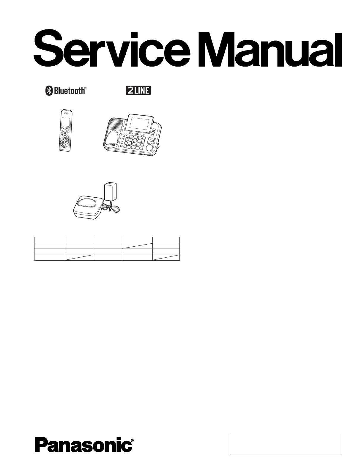
Telephone Equipment
Model No. KX-TG9541B
KX-TG9542B
KX-TGA950B
2-LINE Cordless Phone with Link-to-cell
B: Black Version
(for U.S.A.)
F13
KX-TGA950
(Handset)
(Charger Unit)
Configuration for each model
Model No Base Unit Portable Charger Unit Expandable
KX-TG9541 1 (TG9541) 1 (TGA950) Up to 6
KX-TG9542 1 (TG9541) 2 (TGA950) 1 Up to 6
KX-TGA950* 1 (TGA950) 1
*
KX-TGA950 is an optional accessory, which contains a handset
and a charger.
KX-TG9541
(Base Unit)
© Panasonic System Networks Co., Ltd. 2013
Unauthorized copying and distribution is a
violation of law.
KX-TG9541B/KX-TG9542B/KX- TGA950B
WARNING
This service information is designed for experienced repair technicians only and is not designed for use by the general
public. It does not contain warnings or cautions to advise non-technical individuals of potential dangers in attempting
to service a product. Products powered by electricity should be serviced or repaired only by experienced professional
technicians. Any attempt to service or repair the product or products dealt with in this service information by anyone
else could result in serious injury or death.
IMPORTANT SAFETY NOTICE
There are special components used in this equipment which are important for safety. These parts are marked by
in the Schematic Diagrams, Circuit Board Diagrams, Exploded Views and Replacement Parts List. It is essential that
these critical parts should be replaced with manufacturer's specified parts to prevent shock, fire or other hazards.
Do not modify the original design without permission of manufacturer.
IMPORTANT INFORMATION ABOUT LEAD FREE, (PbF), SOLDERING
If lead free solder was used in the manufacture of this product, the printed circuit boards will be marked PbF.
Standard leaded, (Pb), solder can be used as usual on boards without the PbF mark.
When this mark does appear, please read and follow the special instructions described in this manual on the
use of PbF and how it might be permissible to use Pb solder during service and repair work.
L When you note the serial number, write down all 11 digits. The serial number may be found on the bottom of the unit.
L The illustrations in this Service Manual may vary slightly from the actual product.
2

TABLE OF CONTENTS
1 Safety Precautions ----------------------------------------------- 5
1.1. For Service Technicians --------------------------------- 5
2 Warning-------------------------------------------------------------- 5
2.1. Battery Caution--------------------------------------------- 5
2.2. About Lead Free Solder (Pbf: Pb free)--------------- 5
2.2.1. Suggested PbF Solder ------------------------------ 6
2.3. Discarding of P. C. Board-------------------------------- 6
3 Specifications ----------------------------------------------------- 7
4 Technical Descriptions ----------------------------------------- 8
4.1. Block Diagram (Base Unit) ------------------------------ 8
4.2. Circuit Operation (Base Unit) --------------------------- 9
4.2.1. Outline --------------------------------------------------- 9
4.2.2. Power Supply Circuit--------------------------------10
4.2.3. Telephone Line Interface---------------------------11
4.2.4. Transmitter/Receiver--------------------------------11
4.2.5. Behaviour of Electric Power Failure------------- 11
4.3. Block Diagram (Handset)-------------------------------13
4.4. Circuit Operation (Handset)----------------------------14
4.4.1. Outline --------------------------------------------------14
4.4.2. Power Supply Circuit/Reset Circuit--------------14
4.4.3. Charge Circuit ----------------------------------------14
4.4.4. Battery Low/Power Down Detector--------------15
4.4.5. Speakerphone ----------------------------------------15
4.5. Block Diagram (Charger Unit) -------------------------15
4.6. Signal Route -----------------------------------------------16
5 Location of Controls and Components ------------------20
6 Installation Instructions ---------------------------------------20
7 Operating Instructions-----------------------------------------20
7.1. Registering a Handset to the Base Unit ------------20
7.1.1. Deregistering a Handset ---------------------------20
8 Test Mode ----------------------------------------------------------21
8.1. Engineering Mode ----------------------------------------21
8.1.1. Base Unit ----------------------------------------------21
8.1.2. Handset ------------------------------------------------23
8.2. How to Clear User Setting------------------------------25
8.2.1. Resetting both base unit and handset ----------25
8.2.2. Resetting only handset -----------------------------25
9 Troubleshooting Guide ----------------------------------------26
9.1. Troubleshooting Flowchart -----------------------------26
9.1.1. Check Power------------------------------------------27
9.1.2. Check Battery Charge ------------------------------29
9.1.3. Check Link---------------------------------------------30
9.1.4. Check the RF part -----------------------------------32
9.1.5. Check Handset Transmission --------------------35
9.1.6. Check Handset Reception-------------------------35
9.1.7. Check Caller ID --------------------------------------35
9.1.8. Bell Reception ----------------------------------------36
9.1.9. Check TAM Operation ------------------------------36
9.1.10. Check SP-phone Transmission ------------------37
9.1.11. Check SP-phone Reception ----------------------37
9.1.12. Check USB Function--------------------------------37
9.1.13. Check BT Communication-------------------------38
9.2. Troubleshooting by Symptom (Base Unit and
Charger Unit) ----------------------------------------------40
9.2.1. Check Point (Base Unit) ---------------------------40
9.3. Troubleshooting by Symptom (Handset) -----------42
9.3.1. Check Point (Handset) -----------------------------42
10 Disassembly and Assembly Instructions ---------------45
KX-TG9541B/KX-TG9542B/KX-TGA950B
PAG E PAG E
10.1. Disassembly Instructions------------------------------- 45
10.1.1. Base Unit ---------------------------------------------- 45
10.1.2. Handset ------------------------------------------------ 49
10.2. Assembly Instructions----------------------------------- 50
10.2.1. How to Replace the Base unit LCD------------- 50
10.2.2. How to Replace the Handset LCD -------------- 52
11 Measurements and Adjustments -------------------------- 53
11.1. Equipment Required ------------------------------------ 53
11.2. The Setting Method of JIG----------------------------- 53
11.2.1. Connections (Base Unit) -------------------------- 53
11.2.2. How to install Batch file into P.C. ---------------- 54
11.2.3. Commands-------------------------------------------- 54
11.3. Adjustment Standard (Base Unit) -------------------- 55
11.3.1. Bottom View ------------------------------------------ 55
11.4. The Setting Method of JIG (Handset)--------------- 56
11.4.1. Connections ------------------------------------------ 56
11.4.2. How to install Batch file into P.C. ---------------- 57
11.4.3. Commands-------------------------------------------- 57
11.5. Adjustment Standard (Handset) ---------------------- 58
11.5.1. Component View ------------------------------------ 58
11.6. Things to Do after Replacing IC or X'tal ------------ 59
11.6.1. How to download the data ------------------------ 59
11.7. How to Check the Portable Speaker or
Receiver ---------------------------------------------------- 61
11.8. Frequency Table (MHz)--------------------------------- 61
11.9. Bluetooth Frequency Table ---------------------------- 62
12 Miscellaneous ---------------------------------------------------- 63
12.1. How to Replace the Flat Package IC --------------- 63
12.1.1. Preparation-------------------------------------------- 63
12.1.2. How to Remove the IC ----------------------------- 63
12.1.3. How to Install the IC -------------------------------- 64
12.1.4. How to Remove a Solder Bridge ---------------- 64
12.2. How to Replace the LLP (Leadless Leadframe
Package) IC ----------------------------------------------- 65
12.2.1. Preparation-------------------------------------------- 65
12.2.2. Caution------------------------------------------------- 65
12.2.3. How to Remove the IC ----------------------------- 65
12.2.4. How to Install the IC -------------------------------- 66
12.2.5. How to Remove a Solder Bridge ---------------- 66
12.3. Terminal Guide of the ICs, Transistors and
Diodes ------------------------------------------------------ 67
12.3.1. Base Unit ---------------------------------------------- 67
12.3.2. Handset ------------------------------------------------ 67
13 Schematic Diagram -------------------------------------------- 68
13.1. For Schematic Diagram -------------------------------- 68
13.1.1. Base Unit (Schematic Diagram (Base
Unit_Main)) ------------------------------------------- 68
13.1.2. Handset (Schematic Diagram (Handset))----- 68
13.2. Schematic Diagram (Base Unit_Main)-------------- 69
13.3. Schematic Diagram (Base Unit_Operation) ------- 71
13.4. Schematic Diagram (Base Unit_LCD) -------------- 73
13.5. Schematic Diagram (Base Unit_LED) -------------- 75
13.6. Schematic Diagram (Handset)------------------------ 77
14 Printed Circuit Board ------------------------------------------ 80
14.1. Circuit Board (Base Unit_Main) ---------------------- 80
14.1.1. Component View ------------------------------------ 80
14.1.2. Bottom View ------------------------------------------ 81
14.2. Circuit Board (Base Unit_Operation)---------------- 82
3

KX-TG9541B/KX-TG9542B/KX- TGA950B
14.2.1. Component View ------------------------------------ 82
14.2.2. Bottom View ------------------------------------------ 83
14.3. Circuit Board (Base Unit_LCD) ----------------------- 84
14.4. Circuit Board (Base Unit_TEL Jack) ---------------- 86
14.4.1. Component View ------------------------------------ 86
14.4.2. Bottom View ------------------------------------------ 87
14.5. Circuit Board (Handset)--------------------------------- 88
14.5.1. Component View ------------------------------------ 88
14.5.2. Bottom View ------------------------------------------ 89
15 Exploded View and Replacement Parts List -----------90
15.1. Cabinet and Electrical Parts (Base Unit) ----------- 90
15.2. Cabinet and Electrical Parts (Handset) ------------- 91
15.3. Cabinet and Electrical Parts (Charger Unit) ------- 92
15.4. Accessories and Packing Materials ----------------- 93
15.4.1. KX-TG9541B ----------------------------------------- 93
15.4.2. KX-TG9542B ----------------------------------------- 94
15.4.3. KX-TGA950B ----------------------------------------- 95
15.5. Replacement Parts List --------------------------------- 96
15.5.1. Base Unit ----------------------------------------------96
15.5.2. Handset ---------------------------------------------- 100
15.5.3. Charger Unit ---------------------------------------- 101
15.5.4. Accessories and Packing Materials----------- 101
15.5.5. Screws ----------------------------------------------- 101
15.5.6. Fixtures and Tools --------------------------------- 102
4
KX-TG9541B/KX-TG9542B/KX-TGA950B
Component
Component
pin
Solder
Remove all of the
excess solder
(Slice View)
1 Safety Precautions
1.1. For Service Technicians
• Repair service shall be provided in accordance with repair technology information such as service manual so as to
prevent fires, injury or electric shock, which can be caused by improper repair work.
1. When repair services are provided, neither the products nor their parts or members shall be remodeled.
2. If a lead wire assembly is supplied as a repair part, the lead wire assembly shall be replaced.
3. FASTON terminals shall be plugged straight in and unplugged straight out.
• ICs and LSIs are vulnerable to static electricity.
When repairing, the following precautions will help prevent recurring malfunctions.
1. Cover plastic parts boxes with aluminum foil.
2. Ground the soldering irons.
3. Use a conductive mat on worktable.
4. Do not grasp IC or LSI pins with bare fingers.
2Warning
2.1. Battery Caution
Risk of explosion if battery is replaced by an incorrect type. Dispose of used batteries according to the instructions.
Attention:
A nickel metal hydride battery that is recyclable powers the product you have purchased.
Please call 1-800-8-BATTERY (1-800-822-8837) for information on how to recycle this battery.
2.2. About Lead Free Solder (Pbf: Pb free)
Note:
In the information below, Pb, the symbol for lead in the periodic table of elements, will refer to standard solder or solder that
contains lead.
We will use PbF solder when discussing the lead free solder used in our manufacturing process which is made from Tin (Sn),
Silver (Ag), and Copper (Cu).
This model, and others like it, manufactured using lead free solder will have PbF stamped on the PCB. For service and repair
work we suggest using the same type of solder.
Caution
• PbF solder has a melting point that is 50 F ~ 70 F (30 C ~ 40 C) higher than Pb solder. Please use a soldering iron with
temperature control and adjust it to 700 F ± 20 F (370 C ± 10 C).
• Exercise care while using higher temperature soldering irons.:
Do not heat the PCB for too long time in order to prevent solder splash or damage to the PCB.
• PbF solder will tend to splash if it is heated much higher than its melting point, approximately 1100 F (600 C).
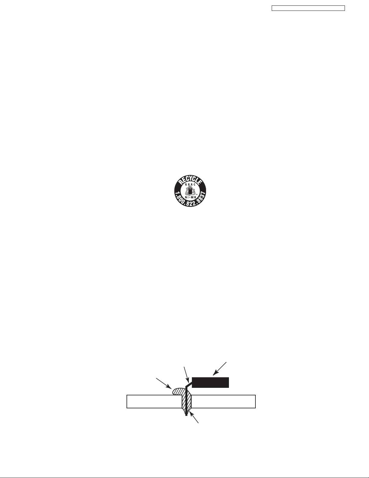
• When applying PbF solder to double layered boards, please check the component side for excess which may flow onto the
opposite side (See the figure below).
5
KX-TG9541B/KX-TG9542B/KX- TGA950B
0.3 mm X 100 g
0.6 mm X 100 g 1.0 mm X 100 g
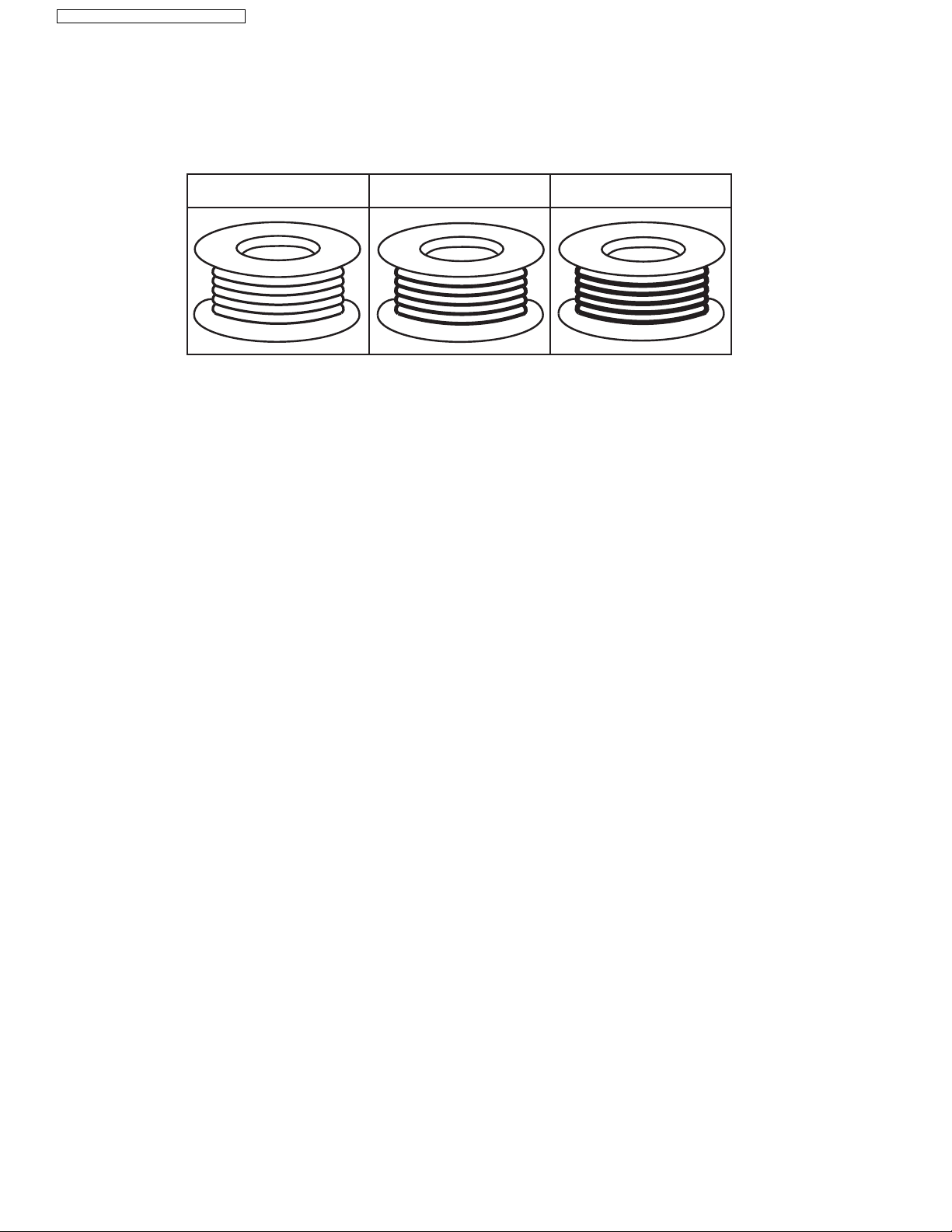
2.2.1. Suggested PbF Solder
There are several types of PbF solder available commercially. While this product is manufactured using Tin, Silver, and Copper
(Sn+Ag+Cu), you can also use Tin and Copper (Sn+Cu), or Tin, Zinc, and Bismuth (Sn+Zn+Bi). Please check the
manufacturer’s specific instructions for the melting points of their products and any precautions for using their product with other
materials.
The following lead free (PbF) solder wire sizes are recommended for service of this product: 0.3 mm, 0.6 mm and 1.0 mm.
2.3. Discarding of P. C. Board
When discarding P. C. Board, delete all personal information such as telephone directory and caller list or scrap P. C. Board.
6
3 Specifications
Power source
Receiving Method
Oscillation Method
Detecting Method
Tolerance of OSC Frequency
Modulation Method
ID Code
Ringer Equivalence No. (REN)
Dialing Mode
Redial
Speed Dialer
Power Consumption
Operating Conditions
Dimensions (H x W x D)
Mass (Weight)
AC Adaptor
(PNLV234Z, 120 V AC, 60 Hz)
Super Heterodyne
PLL synthesizer
Quadrature Discriminator
10.368 MHz ±100 Hz
Frequency Modulation
40 bit
0.1B
Tone (DTMF)/Pulse
Up to 48 digits
Up to 24 digits (Phonebook)
Standby: Approx. 1.2 W
Maximum: Approx. 6.2 W
0 °C - 40 °C (32 °F – 104 °F),
20 % – 80 % relative air humidity
(dry)
Approx. 129mm x 224 mm x 125 mm
Approx. 480 g
Rechargeable Ni-MH battery
AAA (R03) size (1.2 V 550 mAh)
Super Heterodyne
PLL synthesizer
Quadrature Discriminator
10.368 MHz ±100 Hz
Frequency Modulation
40 bit
Tone (DTMF)/Pulse
Up to 48 digits
Up to 24 digits (Phonebook)
7 days at Standby,
15 hours at Talk
0 °C - 40 °C (32 °F – 104 °F),
20 % – 80 % relative air humidity
(dry)
Approx. 168 mm x 48 mm x 31 mm
Approx. 90 g
Base Unit
Portable
Charger
AC Adaptor
(PNLV233AZ 120 V AC, 60 Hz)
Standby: Approx. 0.1 W,
Maximum: Approx. 1.8 W
0 °C - 40 °C (32 °F – 104 °F),
20 % – 80 % relative air humidity
(dry)
Approx. 39 mm x 72 mm x 73 mm
Approx. 100 g
Duplex procedure:
TDMA (Time Division Multiple Access)
Channel
spacing:
1,7
28kHz
Bit rate:
1,152 kbit/s
Modulation:
GFSK (Gaussian Frequency Shift Keying)
RF transmission power:
115 mW (max.)
Voice coding:
ADPCM 32 kbit/s
N Standard:
DECT 6.0 (Digital Enhanced Cordless
Telecommunications 6.0)
Number of channels:
60 Duplex Channels
Frequency range:
Bluetooth wireless technology 2.1
1.92 GHz to 1.93 GHz (DECT)
2.402 GHz to 2.48 GHz (Bluetooth)
USB Charger:
Output voltage: DC 5 V
Output current: 500 mA
N
N
N
N
N
N
N
N
N
KX-TG9541B/KX-TG9542B/KX-TGA950B
Note:
• Design and specifications are subject to change without notice.
Note for service:
• Operation range: Up to 300 m outdoors, Up to 50 m indoors, depending on the condition.
• Analog telephone connection: Telephone Line
• Optional headset: KX-TCA60, KX-TCA93, KX-TCA400, KX-TCA430
7
KX-TG9541B/KX-TG9542B/KX- TGA950B
Q607
Q605
IC606
Q606
IC601
Q103 Q101 D101
IC602
IC603
IC604
IC501
Q701
IC701
T202
Q203
Q201
D201
IC703
T201
PC201
IC201
+
-
䡚
䡚
DiodeBridge
Caller ID Circuit
Bell Detect
Side Tone
Circuit
L1out (TX)
L1in (RX)
L1Hook
L1CID
L1BELL
SPI2 i/f
QSPI i/f
GPIO
Mic
Speaker
GPIO
UART
RF i/f
TAM Flash
(32Mbit)
Flash Memory
Program(16Mbit)
PCM i/f
PCM i/f
PCM i/f
UART
BT Module
Expanded I/O
Key
TP Tx
TP Rx
LSR
L2out(TX)
L2in(RX)
L2Hook
L2CID
L2BELL
+
-
䡚
䡚
DiodeBridge
Caller ID Circuit
Bell Detect
Side Tone
Circuit
DC detect
DC detect
opt isolator
Transformer
LCD i/f
Backlit power
LCD Module
Backlit LED
ADC
ADC
QSPI i/f
Flash Memory
Program(16Mbit)
Expanded I/O
GPIO
S_+1.8V
LDO
CTRL
VBAT 3.4v
RESET Circuit
RESET
Transformer
EEPROM
(128kbit)
M_+3.0V
M_RF+2.5V
M_+1.8V
RF part
USB Conector for
charging
5.0V/500mA
Fuse
5.5V
IC902
LDO 4.0V
FOR LCD
Backlit
4.0V
IC901 , Q903
DC-DC
Step Down
5.5v => 3.4v
VBAT
3.4v
Battery Voltage
Detection
Power Failure
Detection Circuit
Fuse
FET
Switch
IC951
DC-DC
Step Up
2.4v => 3.4v
IC952
Q950
State
Control
IC904
IC902
5.5V
Charge
CTRL
Charge
Terminal
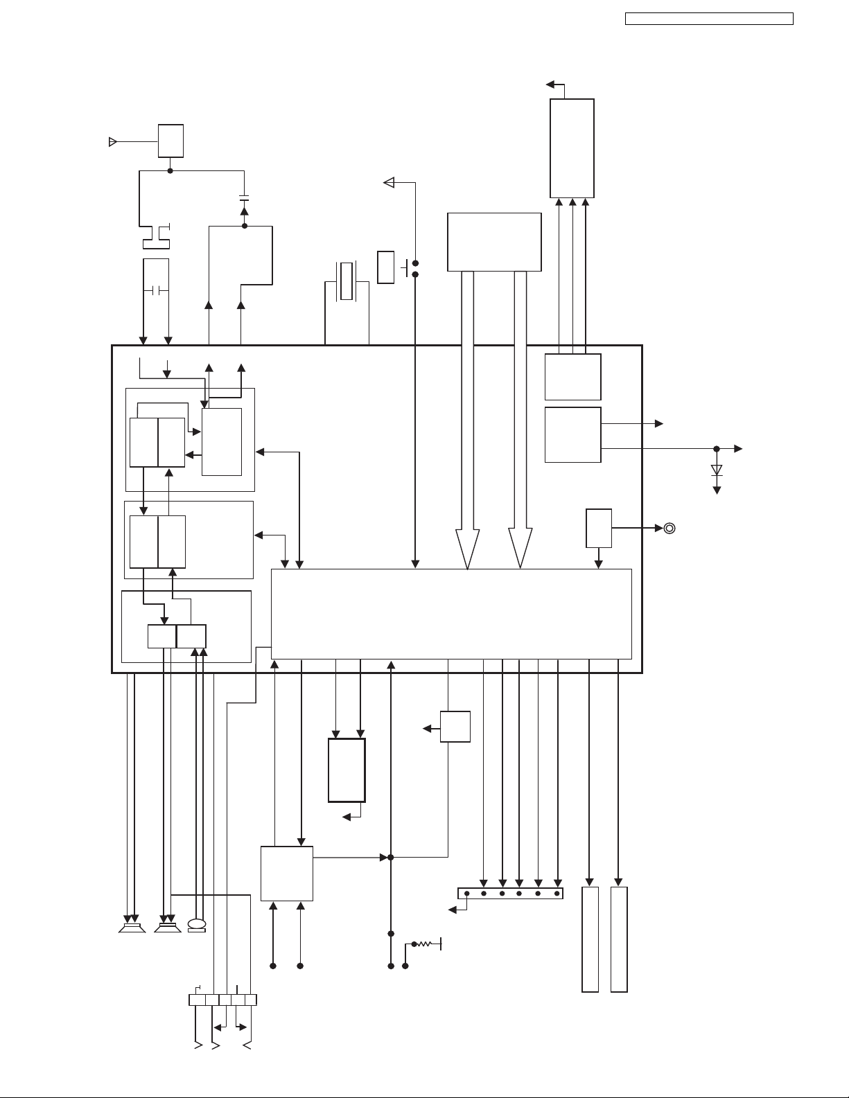
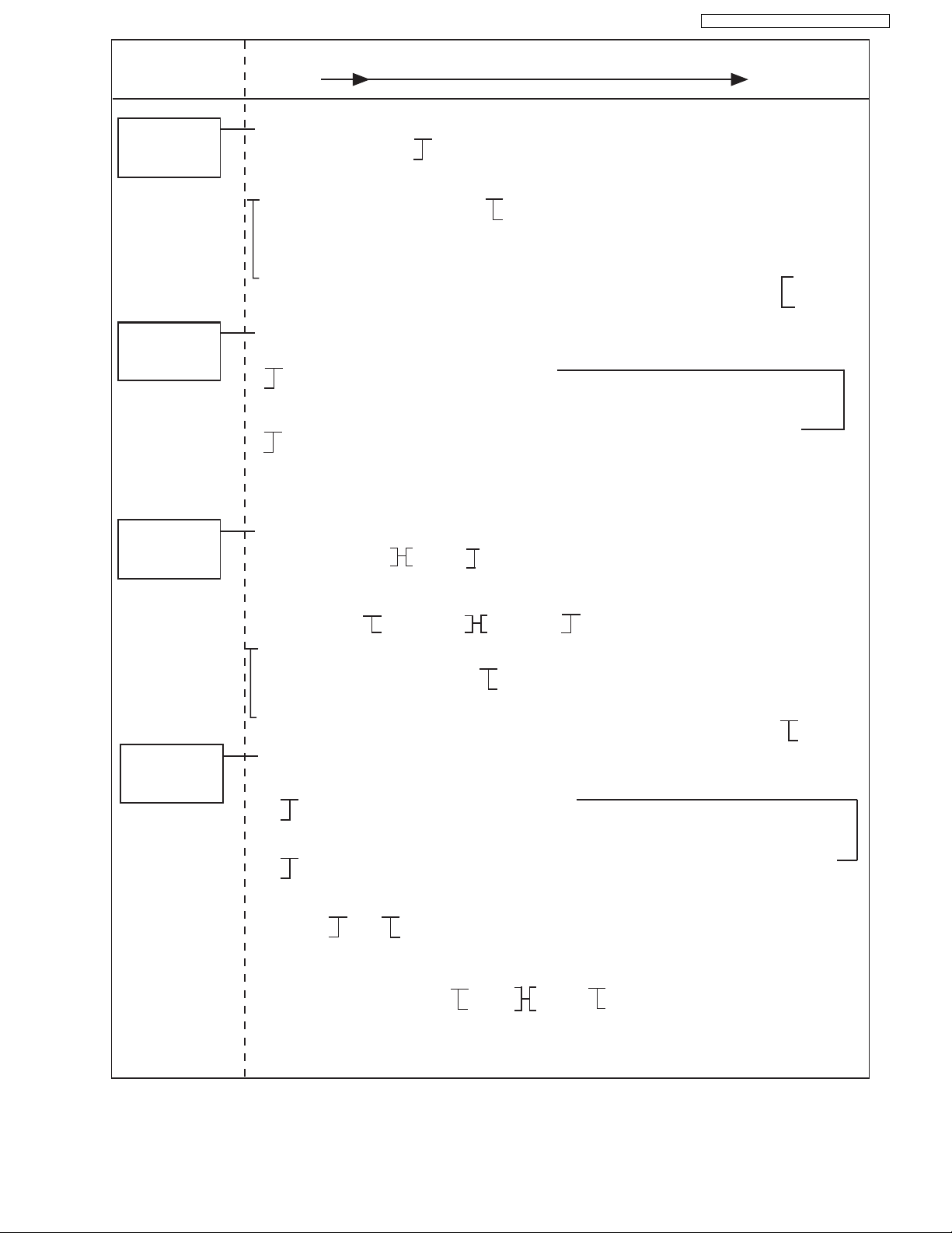
KX-TG9541/9542 BLOCK DIAGRAM (Base Unit_Main)
LDO
CTRL
LDO
CTRL
USB
AC Adaptor
(5.5V)
Battery
LINE1
LINE2
4 Technical Descriptions
4.1. Block Diagram (Base Unit)
8

4.2. Circuit Operation (Base Unit)
4.2.1. Outline
Base unit consists of the following ICs as shown in Block Diagram (Base Unit) (P.8).
• DECT BBIC (BBIC(Master)): IC601
- Handling all the audio, signal and data processing needed in a US DECT base unit
- Controlling the US DECT specific physical layer and radio section (Burst Module Controller section)
- ADPCM code filter for speech encoding and speech decoding (DSP section)
- Echo-cancellation and Echo-suppression (DSP section)
- Any tones (tone, sidetone, ringing tone, etc.) generation (DSP section)
- DTMF receiver (DSP section)
- Clock Generation for RF Module
- ADC, DAC, timer, and power control circuitry
- All interfaces (ex: RF, EEPROM, LED, Analog Front End, etc.)
- PLL Oscillator
- Detector
- Compress/Expander
- First Mixer
- Amplifier for transmission and reception
- Voice data compression and decompression
- Speaker Amp
- SP-Phone MIC Amp
- SP-Phone Speaker Amp
• EEPROM: IC604
- Temporary operating parameters (for RF, etc.)
• FLASH MEMORY 1: IC602
- Voice Prompt (TAM) D/L Area
- ICM/OGM/MEMO Recording Area
• Additionally,
- Power Supply Circuit (+4.0 V, +3.3 V, 3.0V, +2.5 V, +1.8 V output)
- Crystal Circuit (10.368 MHz)
- Telephone Line Interface Circuit
• FLASH MEMORY 2: IC603
- Program DL
• LED Driver: IC102, IC103
• LCD Driver: IC601
• Key Matrix: IC101
• BBIC (Slave) IC701
- ADPCM code filter for speech encoding and speech decoding (DSP section)
- Echo-cancellation and Echo-suppression (DSP section)
- Any tones (tone, sidetone, ringing tone, , etc. ) generation (DSP section)
- DTMF receiver (DSP section)
• FLASH MEMORY IC703
- Program DL
• BT Module (IC501)
- Use for Bluetooth communication
KX-TG9541B/KX-TG9542B/KX-TGA950B
9
KX-TG9541B/KX-TG9542B/KX- TGA950B
A
4.2.2. Power Supply Circuit
The power is supplied to the DECT-BBIC(Master),TAM-Flash,QSPI-Flash,BT-Module,EEPROM,
Expanded-I/O,BBIC(Slave),QSPI-Flash(forSlave),Expanded-I/O;
• BBIC - Master (IC601):
Jack(+5.5v) F900 Q903 D1001(3.3v) Q605 (2.5v) IC601
Jack(+5.5v) F900 Q903 D1001(3.3v) Q606 (1.8v) IC601
Jack(+5.5v) F900 Q903 D1001(3.3v) Q607 (3.0v) IC601
• TAM-Flash (IC602):
Jack(+5.5v) F900 Q903 D1001(3.3v) Q607 (3.0v) IC602
• QSPI-Flash (IC603):
Jack(+5.5v) F900 Q903 D1001(3.3v) Q607 (3.0v) IC603
• BT-Module (IC501):
Jack(+5.5v) F900 Q903 D1001(3.3v) Q607 (3.0v) IC501
• EEPROM (IC604)
Jack(+5.5v) F900 Q903 D1001(3.3v) Q607 (3.0v) D603 IC604
• Expanded-I/O
Jack(+5.5v) F900 Q903 D1001(3.3v) Q607 (3.0v) IC101(separeted PCB)
• BBIC-Slave (IC701)
Jack(+5.5v) F900 Q903 D1001(3.3v) IC701
Jack(+5.5v) F900 Q903 D1001(3.3v) Q703(1.8v) IC701
• OP Amp (IC201):
Jack(+5.5v) F900 Q903 D1001(3.3v) Q703(1.8v) IC201
• QSPI-Flash (IC703):
Jack(+5.5v) F900 Q903 D1001(3.3v) IC701(3.0v) IC703
• Expanded-I/O(IC102,IC103)
Jack(+5.5v) F900 Q903 D1001(3.3v) IC701(3.0v) IC102,IC103
C-Adaptor
Jack
F900
+5.5v
DCDC
Step Down
Q903
IC901
D1001
3.3V
Q605
Q606
2.5V
1.8V
IC601
(BBIC-Master)
M_+3.0V
Q607
D603
IC602
TAM-Flash
IC603
QSPI_Flash
Prog
IC501
BT-Module
IC604
EEPROM
IC101
Expended-I/O
IC102, IC103
Expended I/O,Tr
KEY
LED
Battery Terminal
F901
IC902
IC951
Q950
IC904
State
Control
DCDC
Step Up
IC952
D1002
IC703
QSPI_Flash
Q703
<Fig.101>
10
IC701
BBIC (Slave)
IC201
OP-Amp

KX-TG9541B/KX-TG9542B/KX-TGA950B
4.2.3. Telephone Line Interface
Note:
[ ]: Line 2
<Function>
• Bell signal detection
• Clip signal detection
• ON/OFF hook circuit
Bell & Clip (: Calling Line Identification Presentation: Caller ID) signal detection:
In the standby mode, Q101 [Q201] is open to cut the DC loop current and decrease the ring load.
When ring voltage appears at the L1T (A) [L2T (C)] and L1R (B) [L2R (D)] leads (when the telephone rings), the AC ring voltage
is transferred as follows;
A [C] - C125 [C225] - R121 [R221] - IC601 (H1) [IC701 (15)] (Clip)
B [D] - C127 [C227] - R123 [R223] - IC601 (H2) [IC701 (17)] (Clip)
-- IC601(J2)[IC701(18)] - R637[R725] - R636[R726] - IC601(F3)[IC701(12)] -(Bell)
ON/OFF hook circuit:
In the standby mode, Q101 [Q201] is open, and connected as to cut the DC loop current and to cut the voice signal. The unit is
consequently in an on-hook condition.
When IC601 [IC701] detects a ring signal or press the TALK Key onto the portable, Q102 [Q202] turns on and then Q101,
[Q201, PC201] turns on, thus providing an off-hook condition (DC current flows through the circuit) and the following signal
flow makes the loop current.
A [C] D101 [D201] Q101 [Q201] Q103 [Q203] R108 [R208] D101 [D201] B [D]
4.2.4. Transmitter/Receiver
• Audio Circuits and DTMF tone signal circuits.
Base unit and portable mainly consist of RF and DECT BBIC.
Base unit and portable transmit/receive voice signal and data signal through the antenna on carrier frequency.
Signal Path:
*Refer to Signal Route (P.16).
4.2.4.1. Transmitter Block
The voice signal input from the TEL LINE 1 interface goes to RF ,through DECT BBIC (IC601) as shown in Block Diagram
(Base Unit) (P.8)
The voice signal input from the TEL LINE 2 interface goes to RF though SlaveBBIC(IC701) and BBIC(Master : IC601) as shown
in BlockDiagram.
The voice signal passes through the analog part of IC601 [IC701] where it is amplified and converted to a digital audio stream
signal. The burst switch controller processes this stream performing encryption and scrambling, adding the various other fields
to produce the GAP (Generic Access Profile) standard DECT frame, assigning to a time slot and channel etc.
In IC601, the carrier frequency is changing, and frequency modulated RF signal is generated and amplified, and radiated from
antenna. Portable detects the voice signal or data signal in the circuit same as the following explanation of Receiver Block.
4.2.4.2. Receiver Block
The signal of 1900 MHz band (1920 MHz ~ 1930 MHz) which is input from antenna is input to IC601 as shown in Block
Diagram (Base Unit) (P.8).
In IC601, the signal of 1900 MHz band is downconverted to 864 kHz signal and demodulated,GAP (Generic Access Profile)
standard DECT frames. It passes through the decoding section burst switch controller where it separates out the frame
information and performs de-encryption and de-scrambling as required. It then goes to the DSP section where it is turned back
into analog audio. This is amplified by the analog front end, and goes to the TEL LINE 1 [IC701, TEL LINE 2] Interface.
4.2.5. Behaviour of Electric Power Failure
• This Model can operate in electoric power failure state by battely inserted in base.
When the electrolic failure occurs, temporarily insert 2 standard AAA (R03) size batteries into the base unit.
Both alkaline batteries and rechargeable batteries can be used for the base unit,
but we recommend that you use the charged batteries (supplied) installed in your handset.
11
KX-TG9541B/KX-TG9542B/KX- TGA950B
4.2.5.1. Circuit Operation
When a power failure occurs, IC902 sense power failure because input of +5.5v is going down,
Then IC904 change state, and control FET switch(Q950) to ON, then IC952(DCDC step up) outputs 3.3v
AC-Adaptor
Jack
F900
+5.5V
DCDC
Step Down
Q903
IC901
D1001
3.3V
Battery Terminal
F901
IC902
IC951
Q950
IC904
D1002
State
Control
DCDC
Step Up
IC952
12
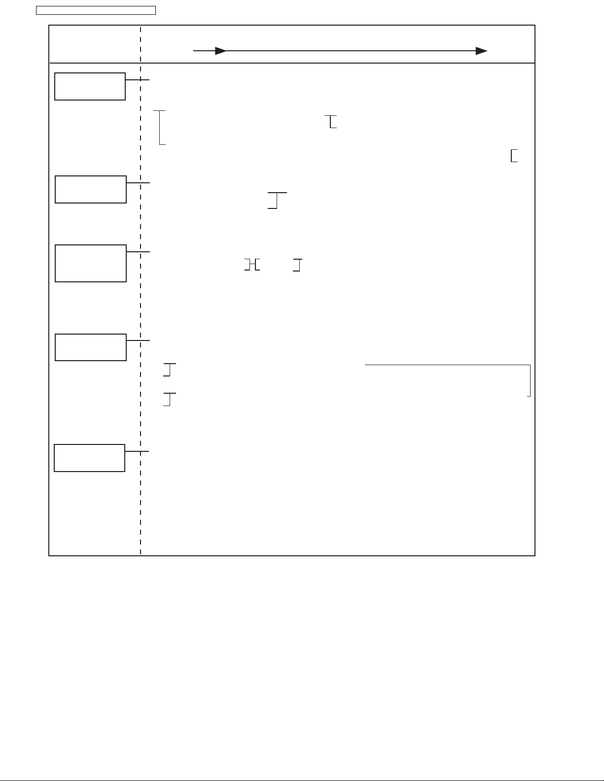
4.3. Block Diagram (Handset)
QSPI
FLASH MEMORY
IC4
SPEAKER
RECEIVER
MIC
CHARGE
CIRCUIT
Q2, Q3, Q4,Q2, Q3, Q4,
Q9, R8
Q9, R8
CHARGE
CONTACTS
CHARGE(+)
CHARGE_CTRL
CHARGE_DET
EEPROM
SCL
SDA
BATTERY
TERMINAL
R45
VBAT
BATT-
1.8 V
Q1
1.8 V
CP 2.8 V
LCD
CD
RESET
CSB
SDA
SCL
CPU
Analog
Front
End
D/A
A/D
35
37
21
22
17
18
34
33
66
67
32
24
736364
76
ADPCM
Codec
Filter
DSP
Speech
Decoding
Speech
Encoding
BMC
Burst
Decoding
ANT1
Burst
Encoding
RF
PLL
MOD/DEMOD
1
2
87
86
RXn
ANT1
RXp
TXp
TXn
7
8
XTAL
X1
10.368
MHz
BATTERY
46
OFF
KEYPAD
ROWS
COLUMNS
57, 58, 59, 60
11, 12, 13, 14, 55
47, 48, 51, 53 QSPI-IO 0-3
44 45
Charge
Pump
CP3V
D3
CP2.8V
CP 4V
BBIC
IC1
IC3
65
KEY LED
61
LDO_CTRL
CP 3.0 V
CP3V
QSPI
Control
52 QSPI-SCK
49 QSPI-CS
KX-TGA950 BLOCK DIAGRAM (Handset)
LCD-BACK LIGHT
77
Reset
Reset
Pin 71
12345
KX-TG9541B/KX-TG9542B/KX-TGA950B
13
KX-TG9541B/KX-TG9542B/KX- TGA950B
Q611
DC+(5.5V) R619 -->R620-->D601-->CHARGE+(Base)-->
R628
-->CHARGE+(Handset) --> QA --> Q3 --> F1--> BATTERY (+)
BATTERY- --> R45 --> GND --> CHARGE-(Handset) --> CHARGE-(Base) --> GND --> DC -(GND)
4.4. Circuit Operation (Handset)
4.4.1. Outline
Handset consists of the following ICs as shown in Block Diagram (Handset) (P.13).
• DECT BBIC (Base Band IC): IC1
- All data signals (forming/analyzing ACK or CMD signal)
- All interfaces (ex: Key, Detector Circuit, Charge, DC/DC Converter, EEPROM, LCD, RF Power Amp.)
- PLL Oscillator
- Detector
- Compress/Expander
- Reception
- Integrated 1.9 GHz PA for DECT
• QSPI FLASH MEMORY: IC4
- Main Program D/L Area
• EEPROM: IC3
- Temporary operating parameters (for RF, etc.)
4.4.2. Power Supply Circuit/Reset Circuit
Circuit Operation:
When power on the Handset, the voltage is as follows;
BATTERY(2.2 V ~ 2.6 V: BATT+) F1 Q1 (1.8 V), IC1-44pin (3.0V)
The Reset signal generates IC1 (71 pin) and 1.8 V.
Battery +
1.8 V
Reset
(IC1_71pin)
4.4.3. Charge Circuit
Circuit Operation:
When charging the handset on the Base Unit, the charge current is as follows;
In this way, the BBIC on Handset detects the fact that the battery is charged.
The charge current is controlled by switching Q9 of Handset.
Refer to Fig.101 in Power Supply Circuit (P.10).
14
4.4.4. Battery Low/Power Down Detector
Charger Terminal
AC Adaptor
Circuit Operation:
“Battery Low” and “Power Down” are detected by BBIC which check the voltage from battery.
The detected voltage is as follows;
• Battery Low
Battery voltage: V(Batt) 2.25 V ± 50 mV
The BBIC detects this level and " " starts flashing.
• Power Down
Battery voltage: V(Batt) 2.0 V ± 50 mV
The BBIC detects this level and power down.
4.4.5. Speakerphone
The hands-free loudspeaker at SP+ and SP- is used to generate the ring alarm.
4.5. Block Diagram (Charger Unit)
KX-TG9541B/KX-TG9542B/KX-TGA950B
15
KX-TG9541B/KX-TG9542B/KX- TGA950B
SIGNAL ROUTE
ROUTE
IN
OUT
SIGNAL
DTMF TONE
TEL OUT
(to Tel Line)
CDL TX
(to Tel Line)
CDL RX
(from Tel Line)
(PORTABLE)
DTMF TONE
TEL IN
(from Tel Line)
B
(BASE UNIT)
Line 1
A
D101 - Q101 - R105 - C121 - R135 - IC601(J2)
D
Line 2
C
D201-Q201- R205 -C205 - R217 -T201(1) -T201(5) - R236 - C221- IC701(19) - IC701 - IC601
B
(BASE UNIT)
Line 1
A
D101 - Q101 - R105 - C121 - R135 - IC601(J2) )
D
Line 2
C
D201 - Q201 - R205 - C205 - R217 - T201(1) - T201(5) - R236 - C221 - IC701(19) -
IC701 - IC601
(BASE UNIT)
from PORTABLE
ANT1 - DA501 IC601(D1)
ANT2 - DA501 IC601(C1)
IC601(A4) C506 DA501- ANT1 - to PORTABLE
IC601(A5) DA501 - ANT2 - to PORTABLE
(PORTABLE)
from BASE UNIT ANT - C801 IC1(1) IC1(21) RECEIVER(+)
IC1(2) IC1(22) RECEIVER(-)
(BASE UNIT)
Line 1
IC601 (K3) - C112 - Q103 - Q101 - D101
A
B
B
Line 2
IC601 - IC701 - IC701(21) - C218 - T202(3) - T202(4) - R215 - C212 - Q203 - Q201 - D201
C
Line 1
IC601(K3) - C112 - Q103 - Q101-D101
A
Line 2
IC601 - IC701 - IC701(21) - C218 - T202(3) - T202(4) - R215 - C212 - Q203 - Q201 - D201
C
D
D
Caller ID
(from Tel Line)
(BASE UNIT)
LINE1
A - C125 - R121- IC601(H1) IC601(A4) C506 DA501- ANT1 - to PORTABLE
B - C127 - R123- IC601(H2) IC601(A5) DA501- ANT2 - to PORTABLE
MIC(+) - C13 - IC1(17) IC1(86) C859 - C801 - ANT to BASE
MIC(-) - C11 - IC1(18) IC1(87)
LINE 2
C - C225 - R221 - IC701(15) IC601
D - C227 - R223 - IC701(17)
4.6. Signal Route
16
KX-TG9541B/KX-TG9542B/KX-TGA950B
SIGNAL ROUTE
Base Unit
SP-PHONE TX
(to Tel Line)
Base Unit
SP-PHONE RX
(from Tel Line)
SIGNAL
IN
ROUTE
(BASE UNIT)
MIC(+) - C651 - IC601(L1)
MIC(-) - C652 - IC601(M1)
Line 1
IC601(K3) - C112 - Q103 - Q101-D101
A
B
Line 2
IC601 - IC701 - IC701(21) - C218 - T202(3) - T202(4) - R215 - C212 - Q203 - Q201 - D201
(BASE UNIT)
Line 1
A
D101 - Q101 - R105 - C121 - R135 - IC601(J2)
B
Line 2
D201- Q201- R205 -C205 -R217 -T201(1) -T201(5) -R236 -C221-IC701(19) -IC701-IC601
C
D
IC601(V9,U9,V6,U6) - Speaker(+)
IC601(V8,U8,V7,U7) - Speaker(-)
OUT
C
D
Portable
SP-PHONE TX
(to Tel Line)
Portable
SP-PHONE RX
(from Tel Line)
(PORTABLE)
MIC(+) - C13 - IC1(17) IC1(86) C859 - C801 - ANT to BASE
MIC(-) - C11 - IC1(18) IC1(87)
(BASE UNIT)
from PORTABLE
ANT1 -DA501 IC601 (D1)
ANT2 -DA501 IC601 (C1)
Line 1
IC601(K3) - C112 - Q103 - Q101-D10
A
B
Line 2
IC601 - IC701 - IC701(21) - C218 - T202(3) - T202(4) - R215 - C212 - Q203 - Q201 - D201 C
D
(BASE UNIT) [ ]: Line 2
Line 1
D101 - Q101 - R105 - C121 - R135 - IC601(J2)
A
B
Line 2
D201 - Q201 - R205 - C205 - R217 -T201(1)- T201(5)- R236- C221- IC701(19)- IC701- IC601
C
D
IC601(A4) C506 DA501- ANT1 - to PORTABLE
IC601(A5) DA501 - ANT2 - to PORTABLE
(PORTABLE)
from BASE UNIT - ANT1 - C801 IC1(1) IC1(35) Speaker(+)
IC1(2) IC1(37) Speaker(-)
17
KX-TG9541B/KX-TG9542B/KX- TGA950B
SIGNAL ROUTE
ROUTE
IN
OUT
SIGNAL
Memo/OGM
Recording
(from Handset)
ICM Recording
(from Tel Line)
(BASE UNIT)
OGM Rec
(from Base Unit)
(BASE UNIT)
MIC(+)
- C651 - IC601(L1)
MIC(- )
- C652 - IC601(M1)
Message Play
(to Base Unit)
(BASE UNIT)
IC602(2) - IC601(P13) -
IC601(V9,U9,V6,U6) - Speaker(+)
IC601(V8,U8,V7,U7) - Speaker(-)
Message Play
(to Tel Line)
(BASE UNIT)
(BASE UNIT)
IC602 (2) - IC601 (P13) -
(HANDSET)
MIC(+) -
C13 - IC1(17) IC1(86) C859 - C801 - ANT to BASE
MIC(- ) - C11- IC1(18) IC1(87)
Line 2
IC601- IC701- IC701(21) -C218 -T202(3) -T202(4) -R215 -C212 - Q203 - Q201- D201
C
D
Line 1
IC601(K3) - C112 - Q103 - Q101-D101
A
B
B
Line 1
A
D101 - Q101 - R105 - C121 - R135 - IC601(J2)
D
Line 2
C
D201-Q201-R205 -C205 -R217-T201(1) -T201(5) -R236 -C221-IC701(19) -IC701- IC601
IC601(P11) - IC602(5)
IC601(P11) - IC602(5)
IC601(P11) - IC602(5)
18
KX-TG9541B/KX-TG9542B/KX-TGA950B
SIGNAL ROUTE
ROUTE
IN
OUT
SIGNAL
CELLULAR
TX (to CELL Phone)
(PORTABLE)
MIC(+) - C13 - IC1(17) IC1(86) C859 - C801 - ANT to BASE
MIC(-) - C11 - IC1(18) IC1(87)
(BASE UNIT)
from PORTABLE ANT1 - DA501 IC601(D1)
ANT2 - DA501 IC601(C1)
IC601 - IC501 - IC501(19) - ANT(BT) - CELL phone
CELLULAR
RX (from CELL
Phone)
CELL phone - ANT(BT) - IC501(19) - IC501 - IC601 -
IC601(A4) C506 DA501- ANT1 - to PORTABLE
IC601(A5) DA501- ANT2 - to PORTABLE
(PORTABLE)
from BASE UNIT ANT - C801 IC1(C1) IC1(21) RECEIVER(+)
IC1(C2) IC1(22) RECEIVER(-)
SIGNAL ROUTE
ROUTE
IN
OUT
SIGNAL
Bluetooth HeadSet
Sound TX (to Tel Line)
From BT HeadSet - ANT(BT) - IC501(19) - IC501 - IC601 -
Line1
IC601(K3) - C112 - Q103 - Q101-D101 A
B
Line 2
IC601 - IC701 - IC701(21) - C218 - T202(3) - T202(4) - R215 - C212 - Q203 - Q201 - D201 -+- C
Bluetooth HeadSet
Sound RX
(from Tel Line)
(BASE UNIT)
Line 1
A D101 - Q101 - R105 - C121 - R135 - IC601(J2)
B
Line 2
C D201 - Q201 - R205 - C205 - R217 - T201(1) - T201(5) - R236 - C221 - IC701(19) - IC701 - IC601
IC601 - IC501 - IC501(19) - ANT(BT) - to BT HeadSet
D
BLUETOOTH
19
KX-TG9541B/KX-TG9542B/KX- TGA950B
Note:
LWhen you purchase an additional portable, refer to the additional portable’s installation manual for
registration.
Registering a handset to the base unit
The supplied handset and base unit are
pre-registered. If for some reason the handset is
not registered to the base unit, re-register the
handset.
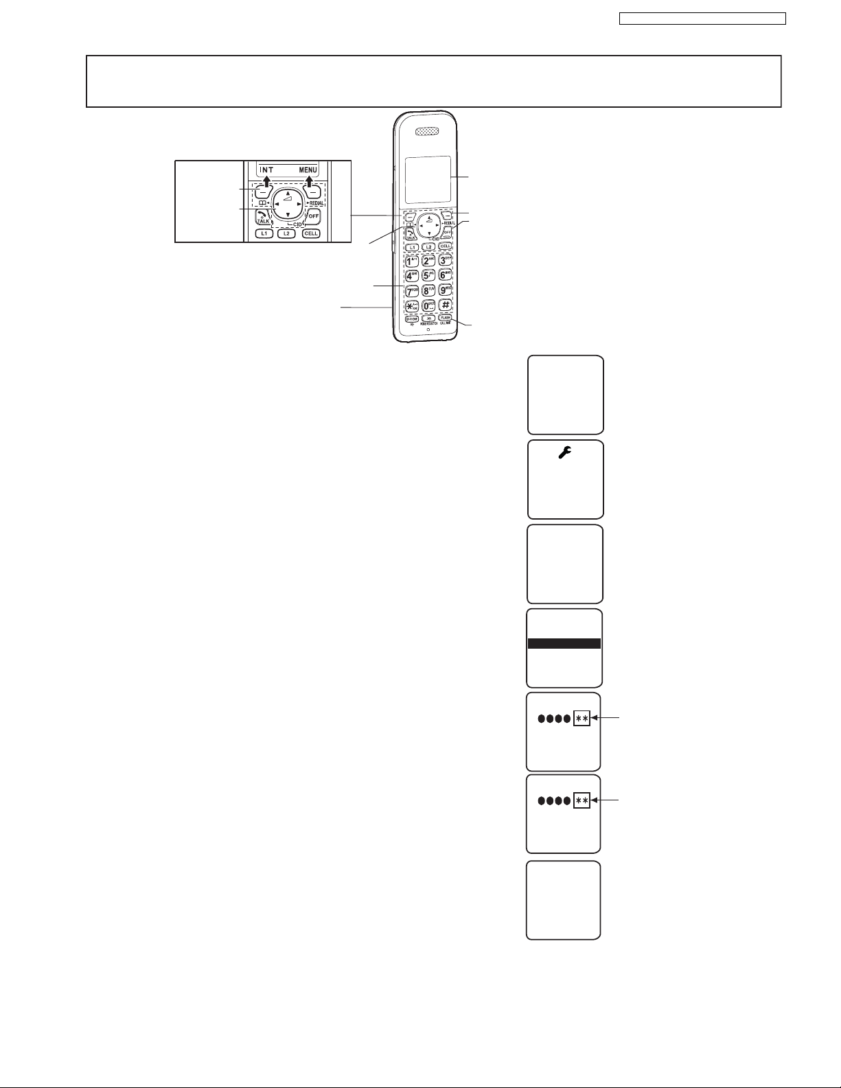
1 Handset:
{MENU
2 Base unit:
Press and hold {LOCATOR} for about 5
seconds until the registration tone sounds.
rIf all registered handsets start ringing, press
{LOCATOR} again to stop, then repeat this
step.
3 Handset:
Press {OK}, then wait until a long beep
sounds.
# 1 3 0
}
A
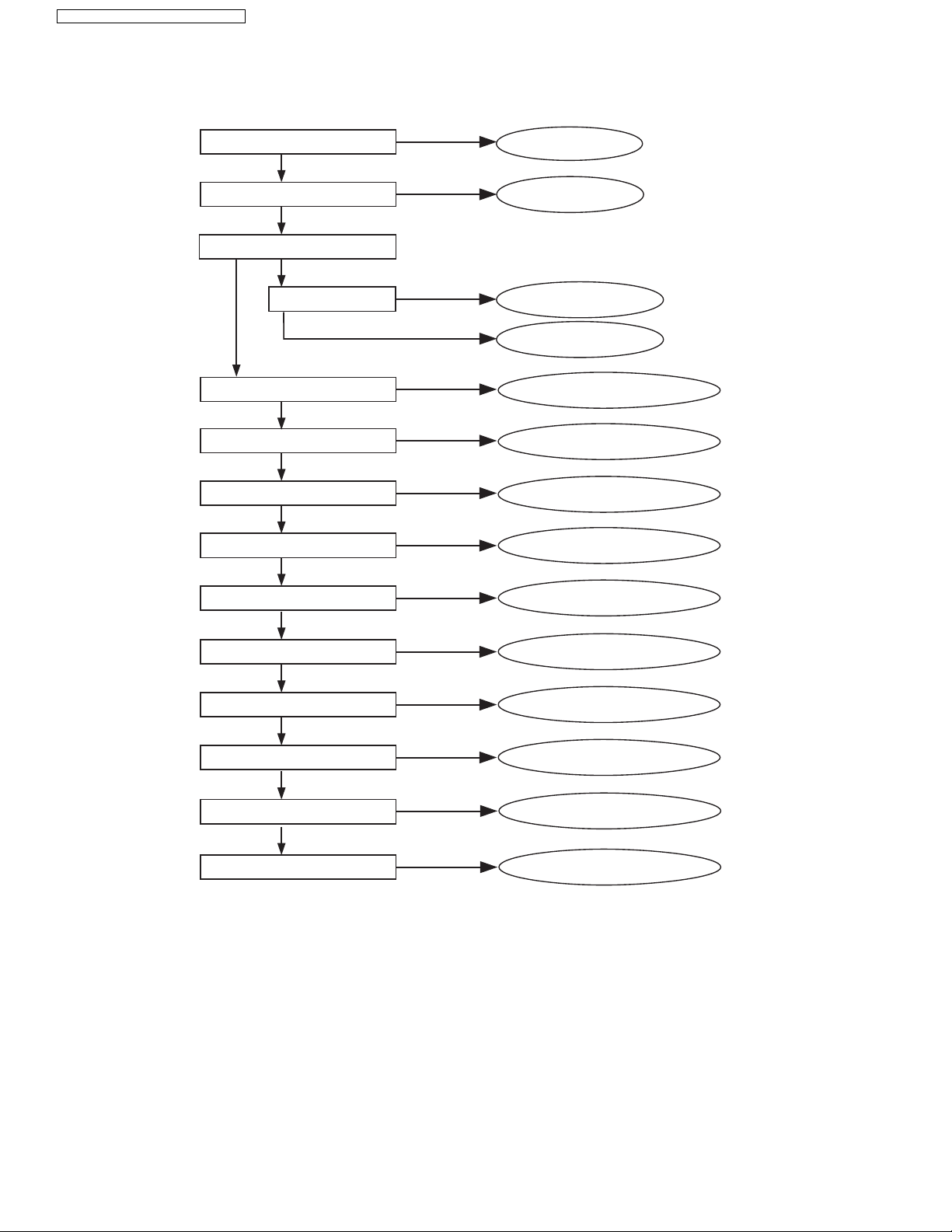
5 Location of Controls and Components
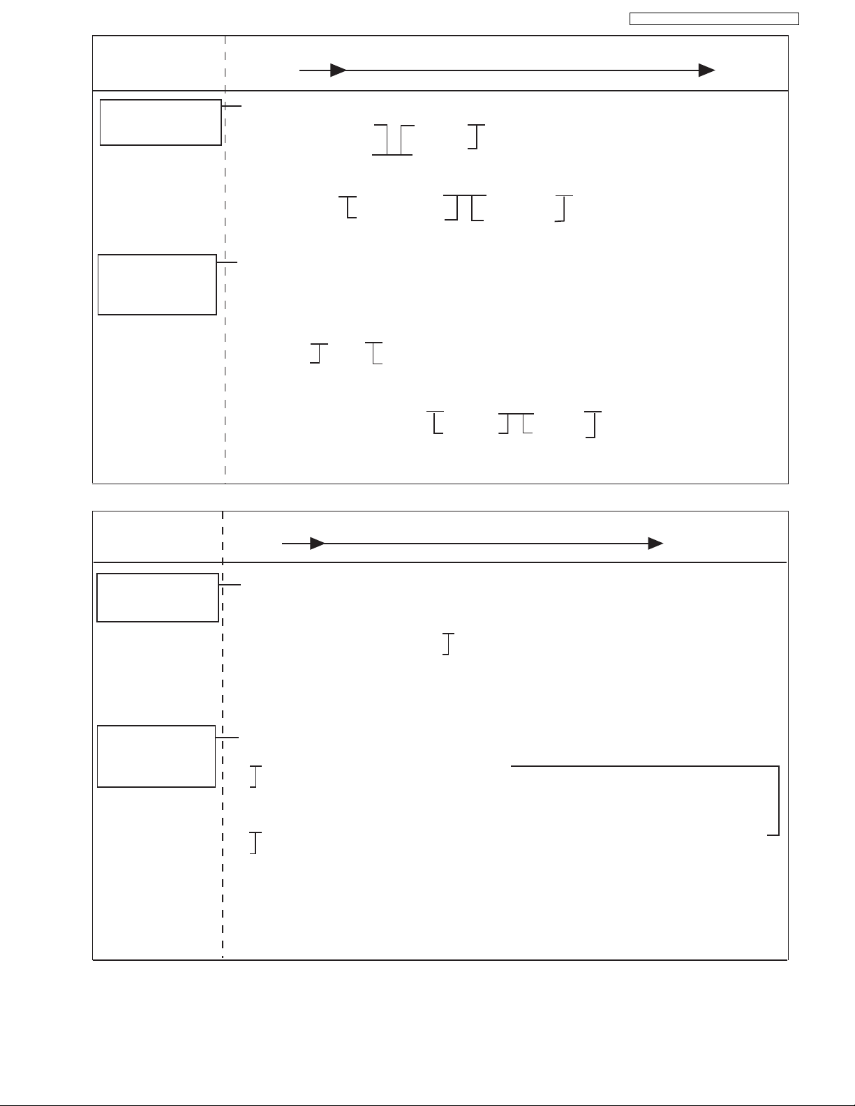
Refer to the Operating Instructions.
Note:
You can download and refer to the Operating Instructions (Instruction book) on TSN Server.
6 Installation Instructions
Refer to the Operating Instructions.
Note:
You can download and refer to the Operating Instructions (Instruction book) on TSN Server.
7 Operating Instructions
Refer to the Operating Instructions.
Note:
You can download and refer to the Operating Instructions (Instruction book) on TSN Server.
7.1. Registering a Handset to the Base Unit
7.1.1. Deregistering a Handset
handset can cancel its own registration to the
base unit, or other handsets registered to the
same base unit. This allows the handset to end its
wireless connection with the system.
Handset / Base unit
1
{MENU} # 1 3 1
rAll handsets registered to the base unit are
displayed.
^
2
{}:: Select the handset you want to cancel.
V
{SELECT}
^
{}
V
3
4
: “Yes” {SELECT}
Proceed with the operation for your unit.
Handset: {OFF}
Base unit: {
EXIT}
20

KX-TG9541B/KX-TG9542B/KX-TGA950B
Important:
Make sure the address on LCD is correct when entering new data. Otherwise, you may ruin the unit.
Data on base unit can be checked and changed by handset.
Prepare base unit (with power on) and handset.
1). Press {MENU}.
2). Select "Initial setting" using or
then press
{SELECT} or {>}.
H/S key operation
H/S LCD
{^} {V}
3). Enter "7", "2", "6", "2", "7", "6", "6", "4".
Note: 7262 7664 = PANA SONI
(see letters printed on dial keys)
See next page
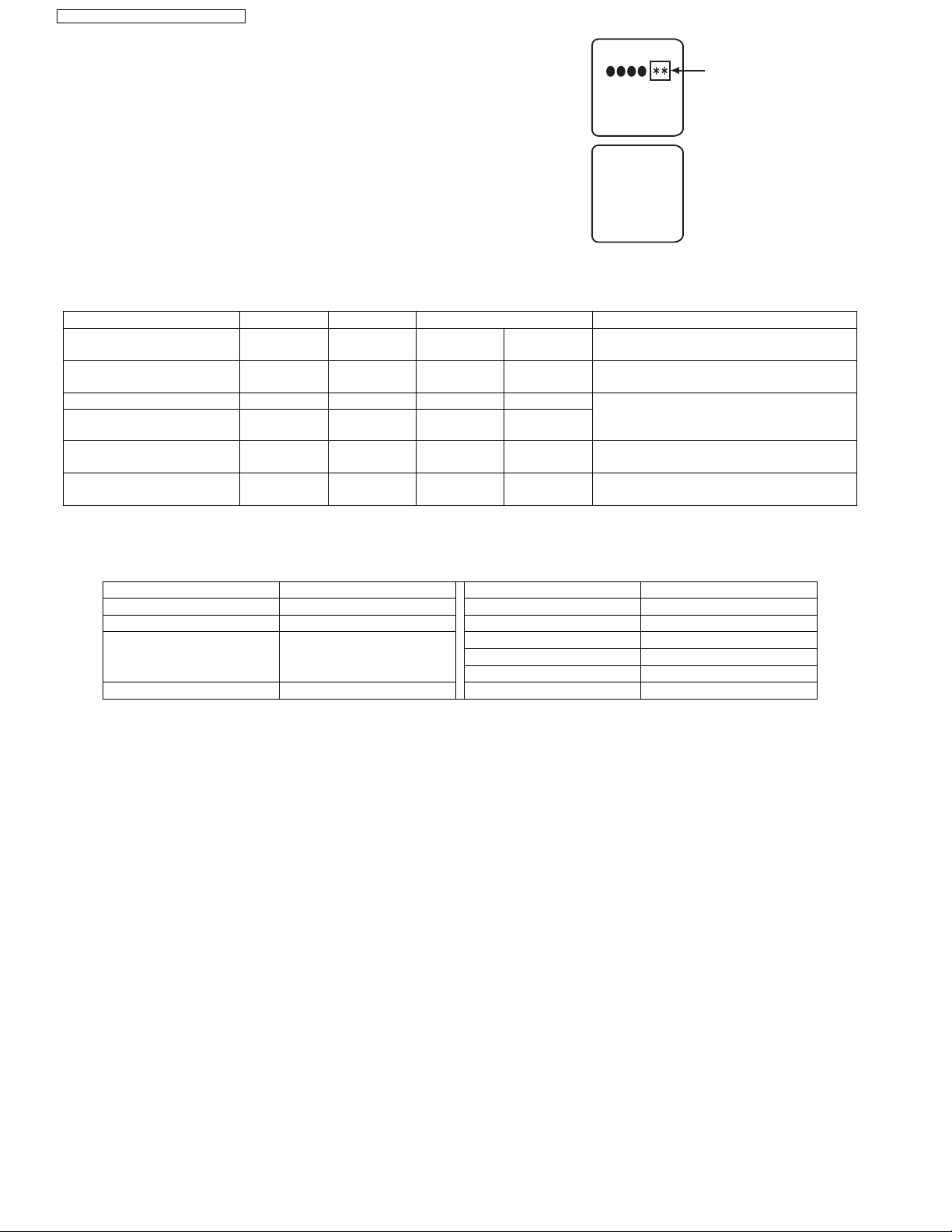
5). Enter "ە", "ە", "ە", "ە" (Address). (*1)
6). Enter "
㸨
", "㸨" (New Data). (*1)
4). Select "Write EEP" using or
then press
{SELECT} or {>}.
{^} {V}
Default Data
Phonebook
^
V
^
V
Initial setting
^
V
Set tel line
Select "Set tel line" using or
then press
{SELECT} or {>}.
{^} {V}
Service Mode
Read EEP
Write EEP
Set Addr.:
Soft keys
Navigator key/
?
(Volume) key
INT
SELECT
INT
SELECT
BACK
SELECT
BACK
SELECT
CLEAR
OK
C
{OFF}
{FLASH}
{CALL WAIT}
Dial keypad
Navigator key/
?
(Volume) key
{REDIAL}
Display
8 Test Mode
8.1. Engineering Mode
8.1.1. Base Unit
21
KX-TG9541B/KX-TG9542B/KX- TGA950B
7). Press {OK} , a long confirmation beep
will be heard.
8).
Press to return to standby mode.
After that, turn the base unit power off and then power on.
New Data
_ _ _ _ _ _
Set Addr.:
Set Addr.:
{OFF}
CLEAR
OK
BACK
Frequently Used Items (Base Unit)
ex.)
Items Address Default Data New Data Remarks
C-ID (FSK) sensitivity(LINE1) 0F7A 0D 06(6dB UP) 03(12dB UP) When hex changes from"0D" to "06" or "03"
C-ID (FSK) sensitivity(LINE2) 0EA1 0D 06(6dB UP) 03(12dB UP) When hex changes from"0D" to "06" or "03"
Frequency 00 07 / 00 08 70/02 - - Use these items in a READ-ONLY mode to
ID 00 02 ~ 00 06 Given value - -
Bell length Melody for LINE1 0542 3C (6 sec) (*3) - - This is time until bell stops ringing.
Bell length Melody for LINE2 0AFA 3C (6 sec) (*3) - - This is time until bell stops ringing.
gain increases by 6dB or 12dB for line1.
gain increases by 6dB or 12dB for line2.
confirm the contents. Careless rewriting may
cause serious damage to the computer system.
(Unit: 100 msec)
(Unit: 100 msec)
Note:
(*1) When you enter the address or New Data, please refer to the table below.
Desired Number (hex) Input Keys Desired Number (hex) Input Keys
0 0 A [Flash] + 0
1 1 B [Flash] + 1
. . C [Flash] + 2
. . D [Flash] + 3
. . E [Flash] + 4
9 9 F [Flash] + 5
22
KX-TG9541B/KX-TG9542B/KX-TGA950B
Important:
Make sure the address on LCD is correct when entering new data. Otherwise, you may ruin the unit.
H/S key operation
H/S LCD
1). Press {MENU}.
2). Select "Initial setting" using or
then press
{SELECT} or {>}.
{^} {V}
3). Enter "7", "2", "6", "2", "7", "6", "6", "4".
Note: 7262 7664 = PANA SONI
(see letters printed on dial keys)
5). Enter "
ە
", "ە", "ە", "ە" (Address). (*1)
7). Press
{OK} , a long confirmation beep
will be heard.
8).
Press to return to standby mode.
After that, remove and reinsert the batteries. Press the Power button for
about 1 second if the power is not turned on.
6). Enter "
㸨
", "㸨" (New Data). (*1)
4). Select "Write EEP" using or
then press
{SELECT} or {>}.
{^} {V}
{OFF}
Default Data
New Data
^
V
Service Mode
Read EEP
Write EEP
Set Addr.:
_ _ _ _ _ _
Set Addr.:
Set Addr.:
Ringer setting
BACK
SELECT
CLEAR
OK
CLEAR
OK
BACK
Phonebook
^
V
INT
SELECT
C
^
V
Initial setting
INT
SELECT
J
BACK
SELECT
Soft keys
Navigator key/
?
(Volume) key
{OFF}
{FLASH}
{CALL WAIT}
Dial keypad
Navigator key/
?
(Volume) key
{REDIAL}
Display
Soft keys
Navigator key/
?
(Volume) key
8.1.2. Handset
23
KX-TG9541B/KX-TG9542B/KX- TGA950B
Frequently Used Items (Handset)
ex.)
Items Address Default Data New Data Possible Adjusted
Value MAX (hex)
Frequency 00 07 / 00 08 70 / 02 - - -
ID 00 02 ~ 00 06 Given value - - -
Possible Adjusted
Value MIN (hex)
Remarks
Note:
(*1) When you enter the address or New Data, please refer to the table below.
Desired Number (hex.) Input Keys Desired Number (hex.) Input Keys
0 0 A [Flash] + 0
1 1 B [Flash] + 1
. . C [Flash] + 2
. . D [Flash] + 3
. . E [Flash] + 4
9 9 F [Flash] + 5
(*2) Use these items in a READ-ONLY mode to confirm the contents. Careless rewriting may cause serious damage to the
handset.
24
KX-TG9541B/KX-TG9542B/KX-TGA950B
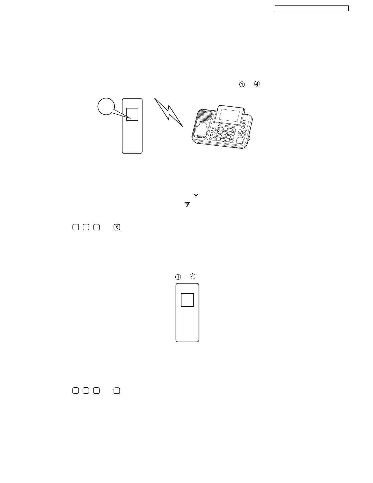
1 Connect the AC adaptor to the base unit and install the charged batteries into the handset.
2 Confirm the handset is registered to the base unit ( lights).
If the handset is not registered to the base unit ( lights), register it. (*1)
3 Lift the handset and press {ih} to put the handset in standby mode.
4 Press , , and key of the handset simultaneously until a confirmation tone is heard.
5 Disconnect the AC adaptor, then remove the battery.
1 5 9
Handset
Base unit
w
1 Install the charged batteries into the handset.
2 Lift the handset and press {ih} to put the handset in standby mode.
4 Remove the battery.
3 Press , , and key of the handset simultaneously until a confirmation tone is heard. (*2)
3 5 7
#
Handset
8.2. How to Clear User Setting
Units are reset to the Factory settings by this operation (Erase recorded Voice messages, stored Phone numbers, Caller list and
etc.)
Note:
• Some menus are not reset. Refer to Operating Instructions (P.20).
• The reset menus differ depending on the following operations.
• This operation should not be performed for a usual repair.
8.2.1. Resetting both base unit and handset
Both the base unit and the registered handset which you did the following steps to are reset. Other registered handsets
will not be reset.
Note:
(*1) Refer to Registering a Handset to a Base Unit in the Operating Instructions.
8.2.2. Resetting only handset
The only handset is reset by doing the following steps to .
Note: (*2)
• The handset registration to the base unit is cancelled.
• If the handset needs to be registered to the base unit, refer to Registering a Handset to a Base Unit in the Operating
Instructions.
• If users do not bring the base unit with them, the registration procedure has to be done by users themselves.
25
KX-TG9541B/KX-TG9542B/KX- TGA950B
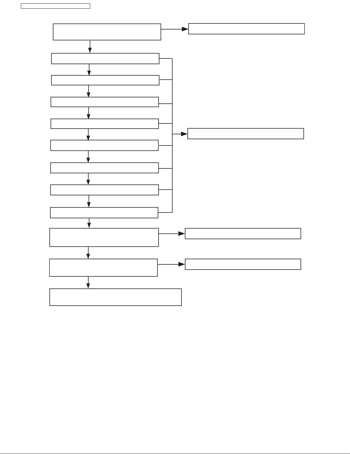
9 Troubleshooting Guide
9.1. Troubleshooting Flowchart
Flow Chart
Power ON Base Unit
OK
Bell
OK
Link
Not Link
OK
Battery Charge
OK
Not Work
No Bell
Not Charge
Check Power
Bell Reception
Check Battery Charge
Check Link
Range
OK
Portable Voice Transmission
OK
Portable Voice Reception
OK
DTMF dial
OK
Caller ID Reception
OK
TAM Operation
OK
SP-Phone Voice Transmission
OK
SP-Phone Voice Reception
OK
BT (Headset/cell)
NG
No Voice
No Voice
No Signal
No Signal
Not Work
No Voice
No Voice
No Voice
Check the RF part
Check Portable Transmission
Check Portable Reception
Signal Route
Check Caller ID
Check TAM Operation
Check SP-phone Transmission
Check SP-phone Reception
Check BT Communication
OK
USB
Cross Reference:
Check Power (P.27)
Bell Reception (P.36)
Check Battery Charge (P.29)
Check Link (P.30)
Check the RF part (P.32)
Check Handset Transmission (P.35)
Check Handset Reception (P.35)
Signal Route (P.16)
Check Caller ID (P.35)
Check TAM Operation (P.36)
Check SP-phone Transmission (P.37)
Check SP-phone Reception (P.37)
Check BT Communication (P.38)
Check USB Function (P.37)
Cannot Charge
26
Check USB Function
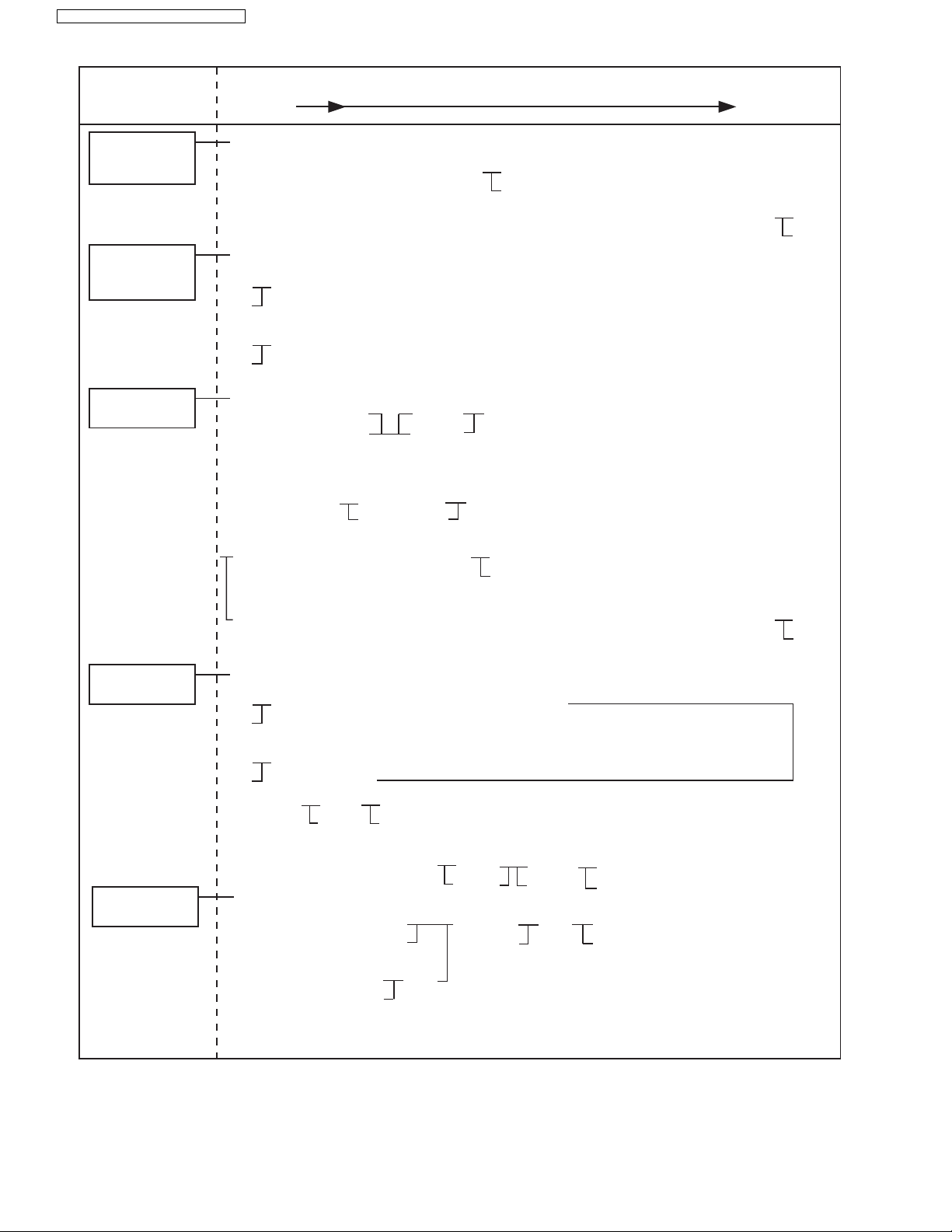
9.1.1. Check Power
9.1.1.1. Base Unit
9.1.1.1.1. Adapter starting
KX-TG9541B/KX-TG9542B/KX-TGA950B
Is the input voltage of IC902:3 about
5.5 V?
YES
Is the output voltage of IC903:1 less than 2.0V?
YES
D1001 cathode voltage is more than 3.2V?
YES
Is the collector of Q607 about 3.0V?
YES
Is the collector of Q606 about 1.8V?
YES
Is the collector of Q606 about 2.5V?
YES
Does BBIC(IC601:B8) oscillate at 10.368MHz?
is BBIC(IC601:B8) High?
YES
Does M CKM (see page.51) oscillate at
10.368MHz? Is IC606:1 High?
NO
NO
NO
Check C902, C903, C904, F900
OK
Check AC Adaptor.
Check Power Circuit.
NO
Check Master_BBIC (IC601) and X601.
Check Slave_BBIC (IC701).
YES
Check Master_BBIC(IC601) and Flash_Memory(IC603).
Check Slave_BBIC(IC701) and Flash_Memory(IC703).
Note:
(*1) Refer to Specifications (P.7) for part number and supply voltage of AC adaptor.
Cross Reference:
Power Supply Circuit (P.10)
27
KX-TG9541B/KX-TG9542B/KX- TGA950B
9.1.1.1.2. Battery starting
Is the input voltage of Battery “+” about
2.35V?
YES
Is the input voltage of IC903:1 less than 2.0V?
YES
Is the input voltage of IC951:1 more than 2.0V?
YES
Is the input voltage of IC904:6 High?
YES
Is the input voltage of IC953:1 High?
NO
Check battery
YES
D1002 cathode voltage is more than 3.2V?
YES
Is the collector of Q607 about 3.0V?
YES
Is the collector of Q606 about 1.8V?
YES
Is the collector of Q606 about 2.5V?
YES
Does BBIC(IC601:B8) oscillate at 10.368MHz?
NO
is BBIC(IC601:B8) High?
YES
Does BBIC(IC701:8) oscillate at 10.368MHz?
NO
is BBIC(IC701:71) High?
YES
Check Master_BBIC(IC601) and Flash_Memory(IC603).
Check Slave_BBIC(IC701) and Flash_Memory(IC703).
Check Power Circuit.
NO
Check Master_BBIC (IC601) and X601.
Check Slave_BBIC (IC701).
Note:
(*1) Refer to Specifications (P.7) for part number and supply voltage of AC adaptor.
Cross Reference:
Power Supply Circuit (P.10)
28
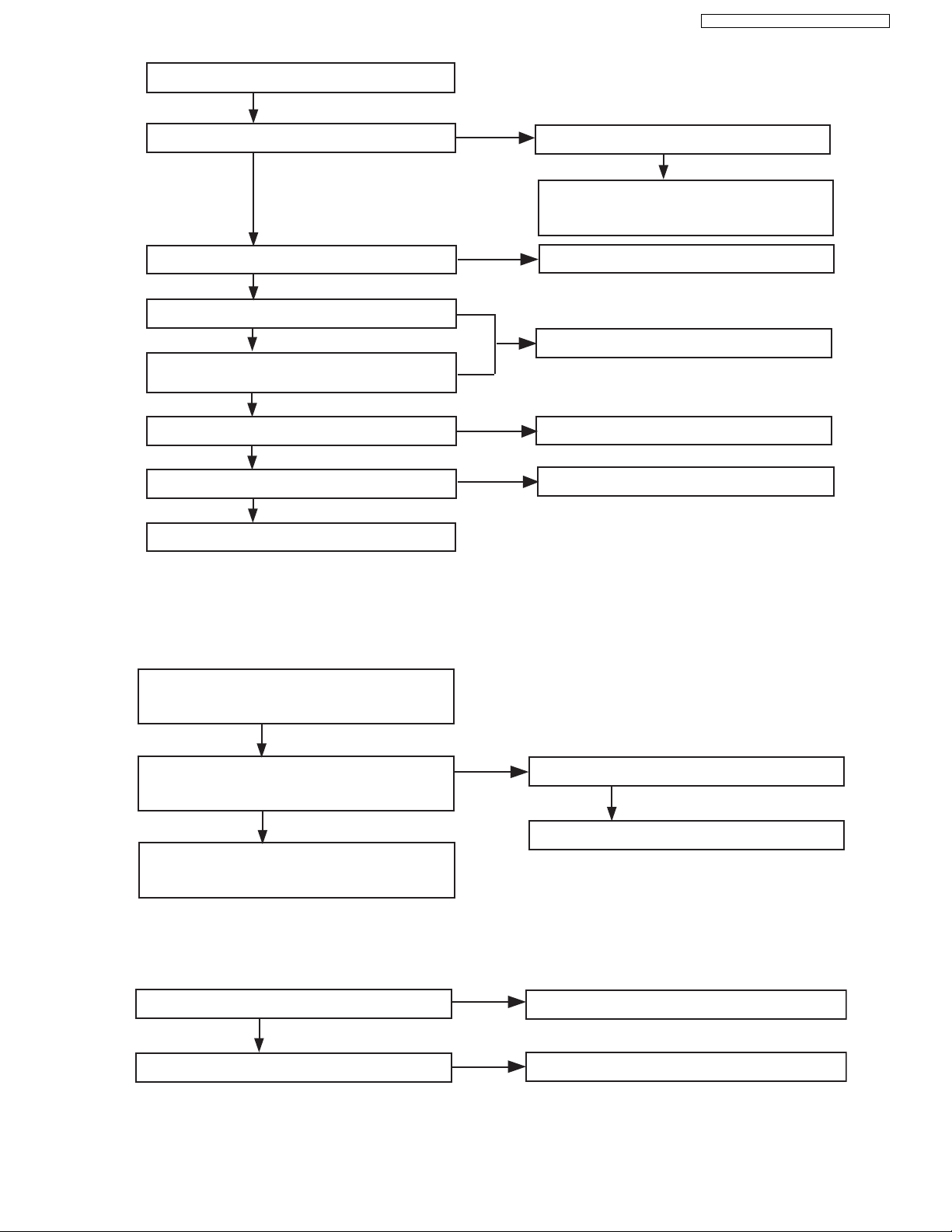
9.1.1.2. Handset
Check Charge Circuit of Base Unit.
Check Handset.
Plug in the AC Power source.
Charge Handset on Base Unit.
Is the voltage of two charge contacts about
3 V or more?
OK
NO
Check Charge Contacts at
Base Unit from mechanical point of view.
YES
Is BBIC (IC601: G3) high at charge state?
Check Charge Circuit.
Check Power of Handset.
Is Check Power OK?
NO
NO
YES
KX-TG9541B/KX-TG9542B/KX-TGA950B
Is the battery inserted BATT+ and BATT-?
Is the voltage of BATT+ 2.3 V more?
Is the voltage of +1.8V about 1.8 V?
Is the voltage of CP3V about 3.0 V?
Is the voltage of CP4V about 4.0V ?
(When LED is On)
Is the voltage of CP2.8V about 2.8 V?
Does BBIC (IC1: 7) oscillate at 10.368 MHz?
YES
YES
YES
YES
YES
YES
YES
NO
Check F1 is not open.
YES
Check the battery and around BATT+ and
BATT- are not shorted.
NO
Check Power Supply Circuit/Reset Circuit .
NO
Check BBIC (IC1).
NO
Check D3.
NO
Check X1.
Check BBIC (IC1).
Cross Reference:
Power Supply Circuit/Reset Circuit (P.14)
9.1.2. Check Battery Charge
9.1.2.1. Base Unit
Cross Reference:
Charge Circuit (P.14)
9.1.2.2. Handset
Cross Reference:
Check Power (P.27)
Charge Circuit (P.14)
29
KX-TG9541B/KX-TG9542B/KX- TGA950B
9.1.3. Check Link
9.1.3.1. Base Unit
Does Base Unit make link with normal working
Portable?
NO
Is the voltage of VBAT about 3.2-3.4 V?
Refer to Check Point...(A).
YES
Is the voltage of VDD2 about 3.05 V?
Refer to Check Point...(B).
YES
Is the voltage of VDD1 about 1.8 V?
Refer to Check Point...(C).
YES
Is the voltage of VDD3 about 2.8 V?
YES
Does the RF clock (CLK) oscillate at 10.368 MHz in
Base Unit Test Mode?
Refer to Check Point...(H).
YES
Is there CMD60 (: DECT Tester)?
YES
NO
NO
NO (*1)
Base Unit is OK. Check Portable.
Check each check point.
NO
OK
Check check point D.
Check around X601 and RF module and adjust
clock frequency.
Refer to Check Point...(H).
YES
Does Base Unit make link with CMD60 in
Base Unit Test Mode?
Refer to Check Point...(K).
Replace with a new Circuit Board.
YES
Is the NTP value OK?
Refer to Check Point...(K).
YES
Is the RSSI level OK?
Refer to Check Point...(L).
NO
Cross Reference:
Power Supply Circuit (P.10)
Check Point (Base Unit) (P.40)
Note:
(*1) Refer to Troubleshooting by Symptom (Base Unit and Charger Unit) (P.40).
30
 Loading...