

Page 1
ORDER NO. MD0605164CE
DVD Recorder
DMR-ES35VEE
DMR-ES35VGC
DMR-ES35VGCS
DMR-ES35VGN
Vol. 1
Colour
(S).......................Silver Type
© 2006 Matsushita Electric Industrial Co., Ltd. All
rights reserved. Unauthorized copying and
distribution is a violation of law.
Page 2
DMR-ES35VGN / DMR-ES35VGC / DMR-ES35 VGCS / DMR-ES35 VEE
CONTENTS
Page Page
1 Safety Precautions 3
1.1. GENERAL GUIDELINES
1.2. Caution for AC Mains Lead (For GC only)
1.3. Before Repair and Adjustment
1.4. Protection Circuitry
2 Prevention of Electro Static Discharge (ESD) to
Electrostatically Sensitive (ES) Devices
3 Precaution of Laser Diode
4 Handling the Lead free Solder
4.1. General description about Lead Free Solder (PbF)
5 Service Navigation
5.1. Service Information
5.2. CAUTION FOR DivX
6 Specifications
7 Accessories
8 Operation Instructions Procedures
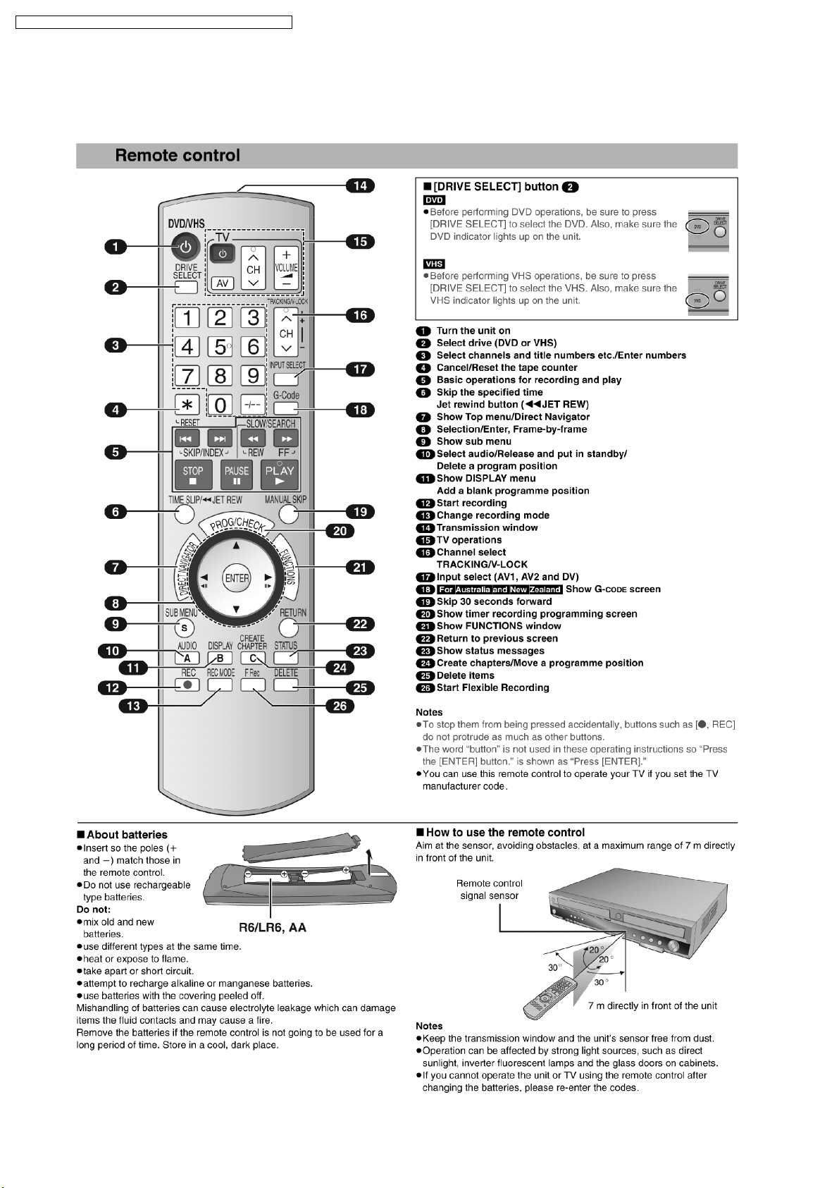
8.1. Remote Control Operation (For GN/GC/GCS)
8.2. Remote Control Operation (For EE)
8.3. Main Unit Operation
8.4. Main Unit Panel Display
8.5. Disc Information
8.6. ABOUT DivX
8.7. Connection to other Devices
8.8. Connection to other Devices
9 Operation Instructions
9.1. (DVD) Taking out the Disc from RAM-Drive Unit when the
Disc cannot be ejected by OPEN/CLOSE button
9.2. (VHS) Removing Cassette Tape manually
10 Service Mode
10.1. (DVD) Self-Diagnosis and Special Mode Setting
10.2. (VHS) Self-Diagnosis and Special Mode Setting
11 Service Fixture & Tools
12 Assembling and Disassembling
12.1. Caution
12.2. Disassembly Flow Chart
12.3. Main Parts Location Diagram
12.4. Caution with inserting cassette tape when disassembling
the unit
12.5. Disassembly of Top Panel
12.6. Disassembly of Nicam Decoder P.C.B.
12.7. Disassembly of Front Panel
12.8. Disassembly of Front Jack P.C.B. & Panel P.C.B.
10
14
16
16
17
18
19
20
25
31
33
35
35
36
38
38
46
49
50
50
51
52
53
54
54
55
55
3
4
5
5
6
7
8
8
9
9
9
12.9. Disassembly of RAM / Digital P.C.B. Module
12.10. Disassembly of DV Jack P.C.B.
12.11. Disassembly of VTR Mechanism Unit
12.12. Disassembly of Rear Panel
12.13. Disassembly of Fan Motor
12.14. Disassembly of Digital I/F P.C.B.
12.15. Main P.C.B.
13 Measurements and Adjustments
13.1. Service Positions
13.2. Caution for Replacing Parts
13.3. Standard Inspection Specifications after Making Repairs
14 Miscellane ous
14.1. Abbreviations
15 Voltage Measurement and Waveform Chart
15.1. Voltage Measurement
15.2. Waveform Chart
16 Wiring Diagram
17 Block Diagram
17.1. Analog Audio Block Diagram
17.2. Analog Timer Block Diagram
17.3. Analog Video Block Diagram
17.4. Power Supply Block Diagram
17.5. System Control & ServoBlock Diagram
18 Notes of Schematic Diagram
19 Schematic Diagram
19.1. DIGITAL IF CIRCUIT
19.2. MAIN CIRCUIT
19.3. PANEL CIRCUIT
19.4. FRONT JACK CIRCUIT
19.5. NICAM DECODER CIRCUIT
19.6. DV JACK CIRCUIT
20 Printed Circuit Board
20.1. DIGITAL I/F P.C.B
20.2. MAIN P.C.B
20.3. PANEL P.C.B, FRONT JACK P.C.B, NICAM DECODER
P.C.B and DV JACK P.C.B
21 Exploded Views
21.1. Casing Parts & Mechanism Section1
21.2. Casing Parts & Mechanism Section 2
21.3. VHS Mechanism Section
21.4. Packing
22 Replacement Parts List
56
57
58
59
59
59
60
61
61
64
69
71
71
77
77
82
85
87
87
88
89
91
93
95
97
97
102
115
116
117
118
123
123
124
125
127
127
128
129
130
131
2
Page 3
DMR-ES35VGN / DMR-ES35VGC / DMR-ES35 VGCS / DMR-ES35 VEE
1 Safety Precautions
1.1. GENERAL GUIDELINES
1. When servicing, observe the original lead dress. If a short circuit is found, replace all parts which have been overheated or
damaged by the short circuit.
2. After servicing, ensure that all the protective devices such as insulation barriers, insulation papers shields are properly installed.
3. After servicing, check for leakage current checks to prevent from being expose d to shock hazards.
1.1.1. LEAKAGE CURRENT COLD CHECK
1. Unplug the AC cord and connect a jumper between the two prongs on the plug.
2. Using an ohmmeter measure the resistance value, between the jumpered AC plug and each exposed metallic cabinet part on
the equipment such as screwheads, connectors, control shafts, etc. When the exposed metallic part has a return path to the
chassis, the reading should be between 1MΩ and 5.2Ω.
When the exposed metal does not have a return path to the chassis, the reading must be
.
Figure. 1
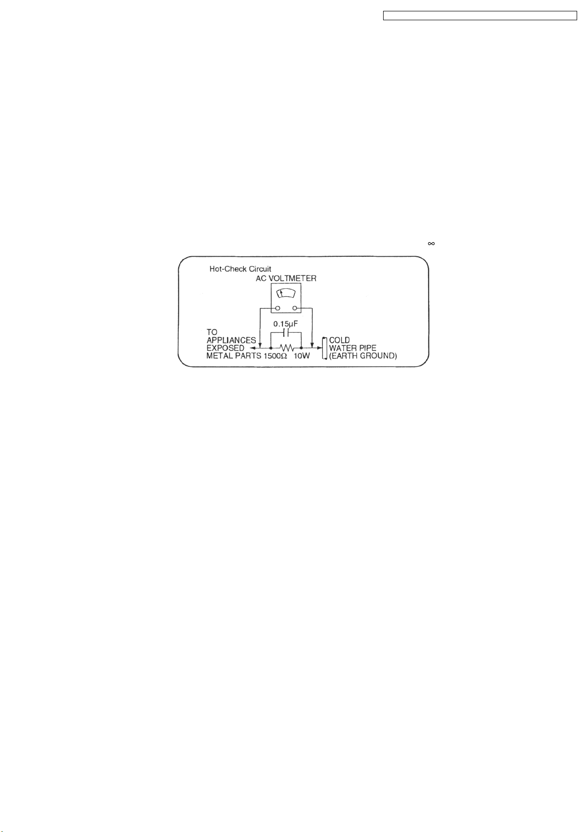
1.1.2. LEAKAGE CURRENT HOT CHECK (See Figure 1.)
1. Plug the AC cord directly into the AC outlet. Do not use an isolation transfo rmer for this check.
2. Connect a 1.5kΩ, 10 watts resistor, in parallel with a 0.15µF capacitors, between each exposed metallic part on the set and a
good earth ground such as a water pipe, as shown in Figure 1.
3. Use an AC voltmeter, with 1000 ohms/volt or more sensitivity, to measure the potential across the resistor.
4. Check each exposed metallic part, and measure the voltage at each point.
5. Reverse the AC plug in the AC outlet and repeat each of the above measurements.
6. The potential at any point should not exceed 0.75 volts RMS. A leakage current tester (Simpson Model 229 or equivalent) may
be used to make the hot checks, leakage current must not exceed 1/2 milliamp. should the measurement is outside of the limits
specified, there is a possibility of a shock hazard, and the equipment should be repaired and re-checked before it is returned
to the customer.
3
Page 4
DMR-ES35VGN / DMR-ES35VGC / DMR-ES35 VGCS / DMR-ES35 VEE
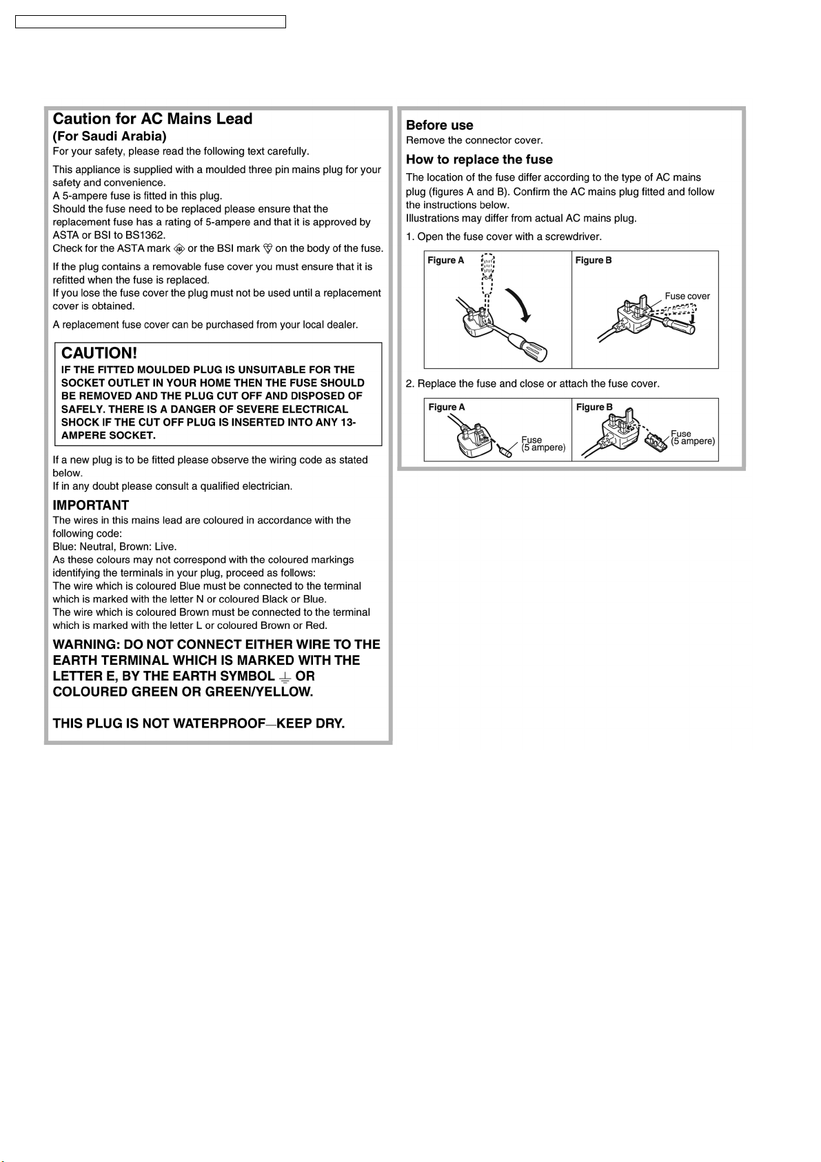
1.2. Caution for AC Mains Lead (For GC only)
4
Page 5

DMR-ES35VGN / DMR-ES35VGC / DMR-ES35 VGCS / DMR-ES35 VEE
1.3. Before Repair and Adjustment
Disconnect AC power, discharge Power Supply Capacitors C11101, C11104, C11105 and C11106 through a 10Ω, 1W resistor to
ground.
DO NOT SHORT-CIRCUIT DIRECTLY (with a screwdriver blade, for instance), as this may destroy solid state devices.
After repairs are completed, restore power gradually using a variac, to avoid overcurrent.
1.4. Protection Circuitry
The protection circuitry may have operated if either of the following conditions are noticed:
· No sound is heard when the power is turned on.
· Sound stops during a performance.
The function of this circuitry is to prevent circuitry damage if, for example, the positive and negative speaker connection wires are
"shorted", or if speaker systems with an impedance less than the indicated rated impedance of the amplifier are used.
If this occurs, follow the procedure outlines below:
1. Turn off the power.
2. Determine the cause of the problem and correct it.
3. Turn on the power once again after one minute.
Note:
When the protection circuitry functions, the unit will not operate unless the power is first turned off and then on again.
5
Page 6
DMR-ES35VGN / DMR-ES35VGC / DMR-ES35 VGCS / DMR-ES35 VEE
2 Prevention of Electro Static Discharge (ESD) to
Electrostatically Sensitive (ES) Devices
Some semiconductor (solid state) devices can be damaged easily by electricity. Such components commonly are called
Electrostatically Sensitive (ES) Devices. Examples of typical ES devices are integrated circuits and some field-effect transistors and
semiconductor “chip” components. The following techniques should be used to help reduce the incidence of component damage
caused by electro static discharge (ESD).
1. Immediately before handling any semiconductor component or semiconductor-equiped assembly, drain off any ESD on your
body by touching a known earth ground. Alternatively, obtain and wear a commercially available discharging ESD wrist strap,
which should be removed for potential shock reasons prior to applyin g power to the unit under test.
2. After removing an electrical assembly equiped with ES devices, place the assembly on a conductive surface such as aluminium
foil, to prevent electrostatic charge build up or exposure of the assembly.
3. Use only a grounded-tip soldering iron to solder or unsolder ES devices.
4. Use only an anti-static solder removal device. Some solder removal devices not classified as “anti-static (ESD protected)” can
generate electrical charge to damage ES devices.
5. Do not use freon-propelled chemicals. These can generate electrical charges sufficient to damage ES devices.
6. Do not remove a replacement ES device from its protective package until immediately before you are ready to install it. (Most
replacement ES devices are packaged with leads electrically shorted together by conductive foam, aluminium foil or
comparable conductive material).
7. Immediately before removing the protective material from the leads of a replacement ES device, touch the protective material
to the chassis or circuit assembly into which the device will be installed.
Caution
Be sure no power is applied to the chassis or circuit, and observe all other safety precautions.
8. Minimize bodily motions when handling unpackaged replacement ES devices. (Otherwise harmless motion such as the
brushing together of your clothes fabric or the lifting of your foot from a carpeted floor can generate static electricity (ESD)
sufficient to damage an ES device).
6
Page 7
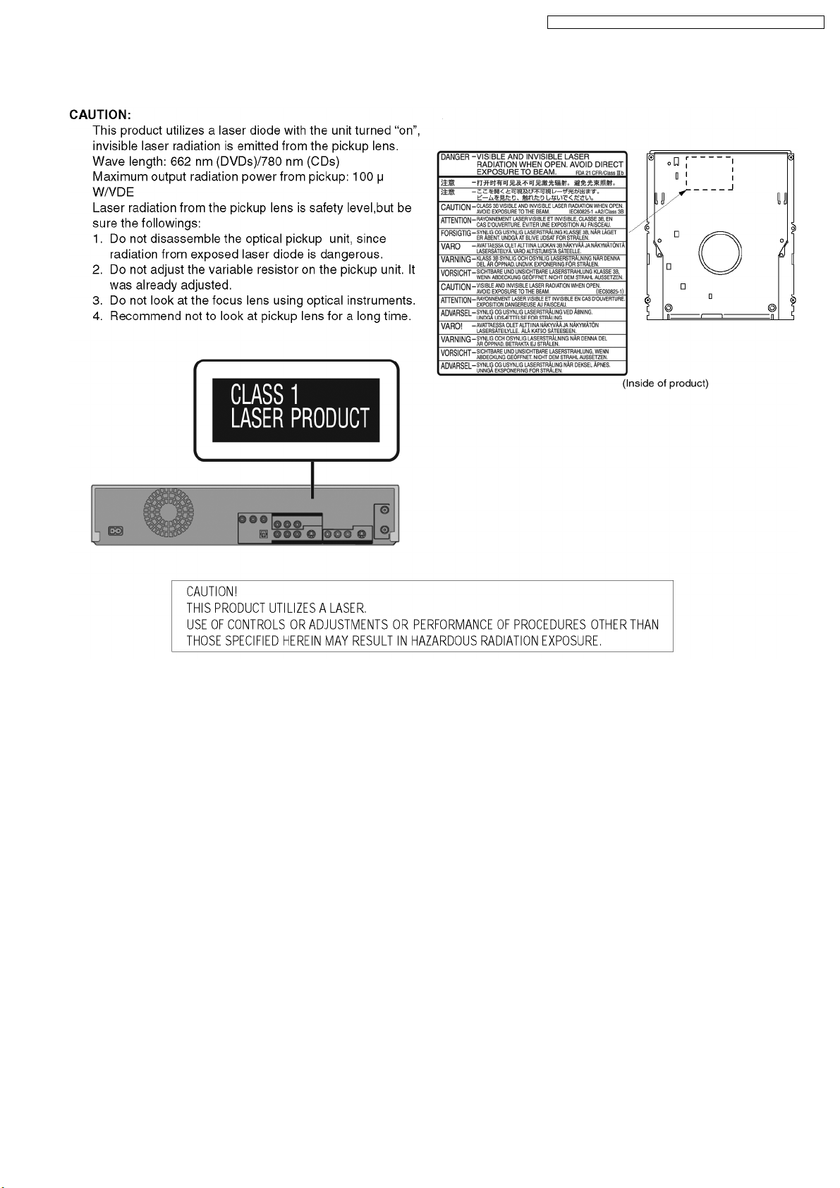
3 Precaution of Laser Diode
DMR-ES35VGN / DMR-ES35VGC / DMR-ES35 VGCS / DMR-ES35 VEE
7
Page 8

DMR-ES35VGN / DMR-ES35VGC / DMR-ES35 VGCS / DMR-ES35 VEE
4 Handling the Lead free Solder
4.1. General description about Lead Free Solder (PbF)
The lead free solder has been used in the mounting process of all electrical components on the printed circuit boards used for this
equipment in considering the globally environmental conservation.
The normal solder is the alloy of tin (Sn) and lead (Pb). On the other hand, the lead free solder is the alloy mainly consists of tin
(Sn), silver (Ag) and Copper (Cu), and the melting point of the lead free solder is higher approx.30 degrees C (86°F) more than that
of the normal solder.
Definition of PCB Lead Free Solder being used
The letter of “PbF” is printed either foil side or components side on the PCB using the lead free solder.
(See right figure)
Service caution for repair work using Lead Free Solder (PbF)
· The lead free solder has to be used when repairing the equipment for which the lead free solder is used.
(Definition: The letter of “PbF” is printed on the PCB using the lead free solder.)
· To put lead free solder, it should be well molten and mixed with the original lead free solder.
· Remove the remaining lead free solder on the PCB cleanly for soldering of the new IC.
· Since the melting point of the lead free solder is higher than that of the normal lead solder, it takes the longer time to melt
the lead free solder.
· Use the soldering iron (more than 70W) equipped with the temperature control after setting the temperature at 350±30
degrees C (662±86°F).
Recommended Lead Free Solder (Service Parts Route.)
· The following 3 types of lead free solder are available through the service parts route.
RFKZ03D01K-----------(0.3mm 100g Reel)
RFKZ06D01K-----------(0.6mm 100g Reel)
RFKZ10D01K-----------(1.0mm 100g Reel)
Note
* Ingredient: Tin (Sn), 96.5%, Silver (Ag) 3.0%, Copper (Cu) 0.5%, Cobalt (Co) / Germanium (Ge) 0.1 to 0.3%
8
Page 9
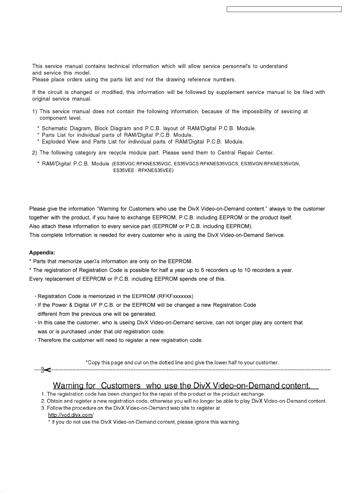
5 Service Navigation
5.1. Service Information
DMR-ES35VGN / DMR-ES35VGC / DMR-ES35 VGCS / DMR-ES35 VEE
5.2. CAUTION FOR DivX
9
Page 10
DMR-ES35VGN / DMR-ES35VGC / DMR-ES35 VGCS / DMR-ES35 VEE
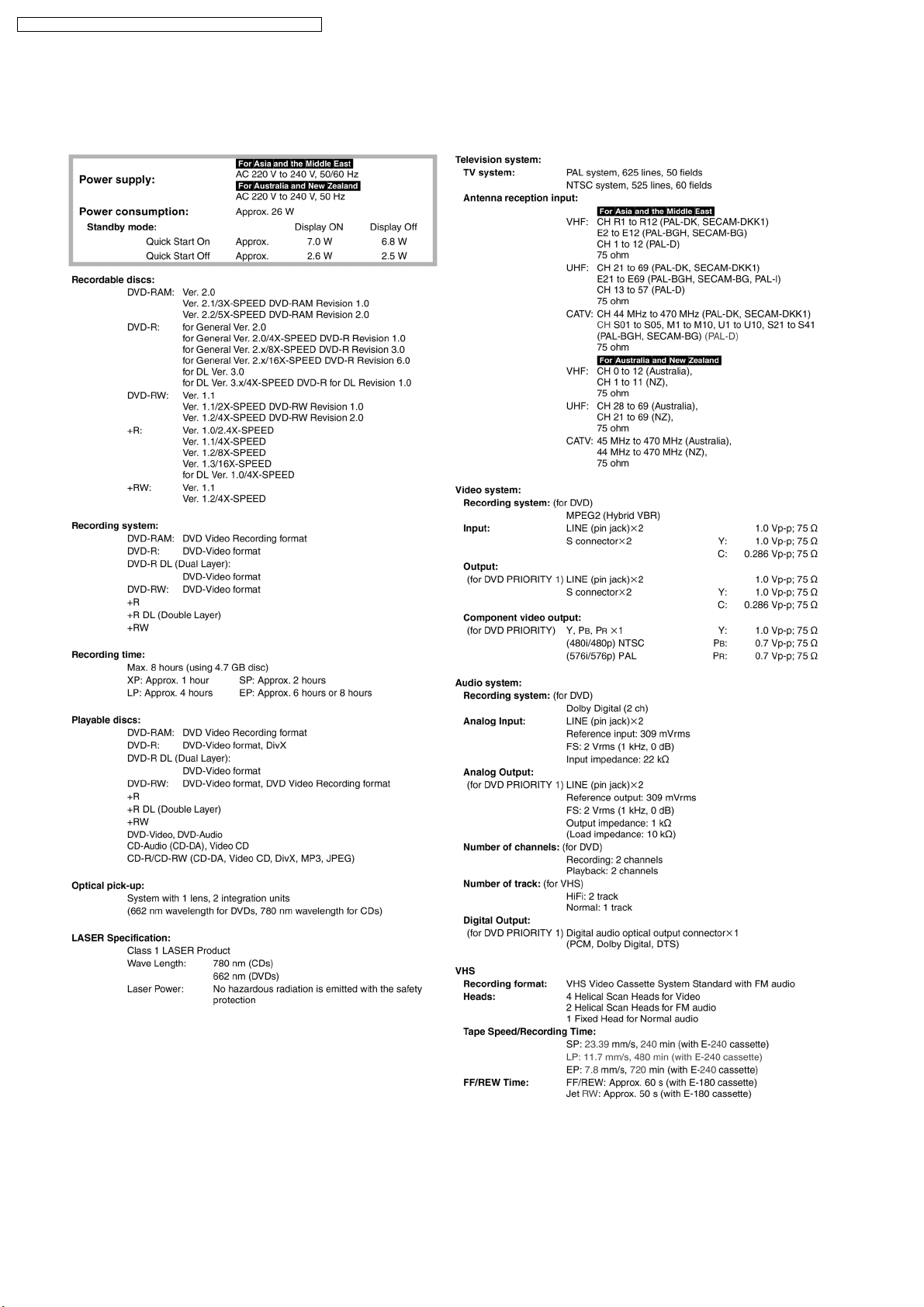
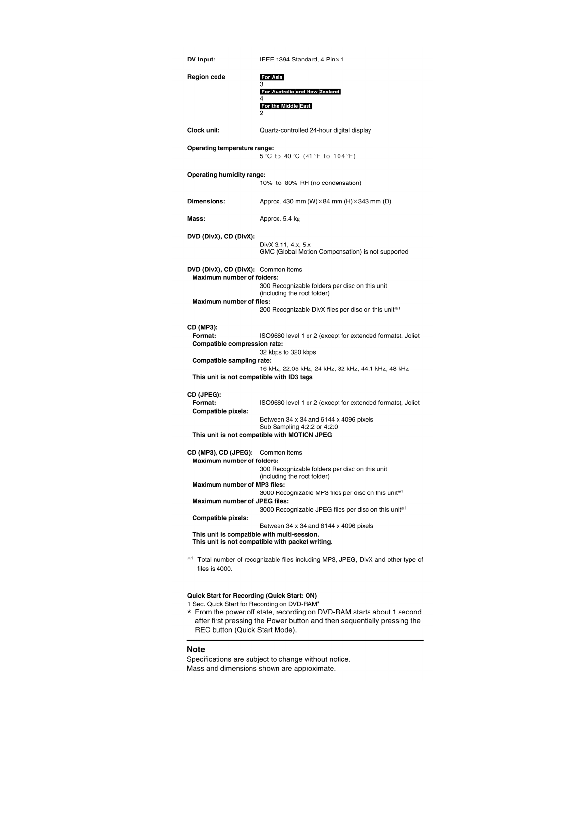
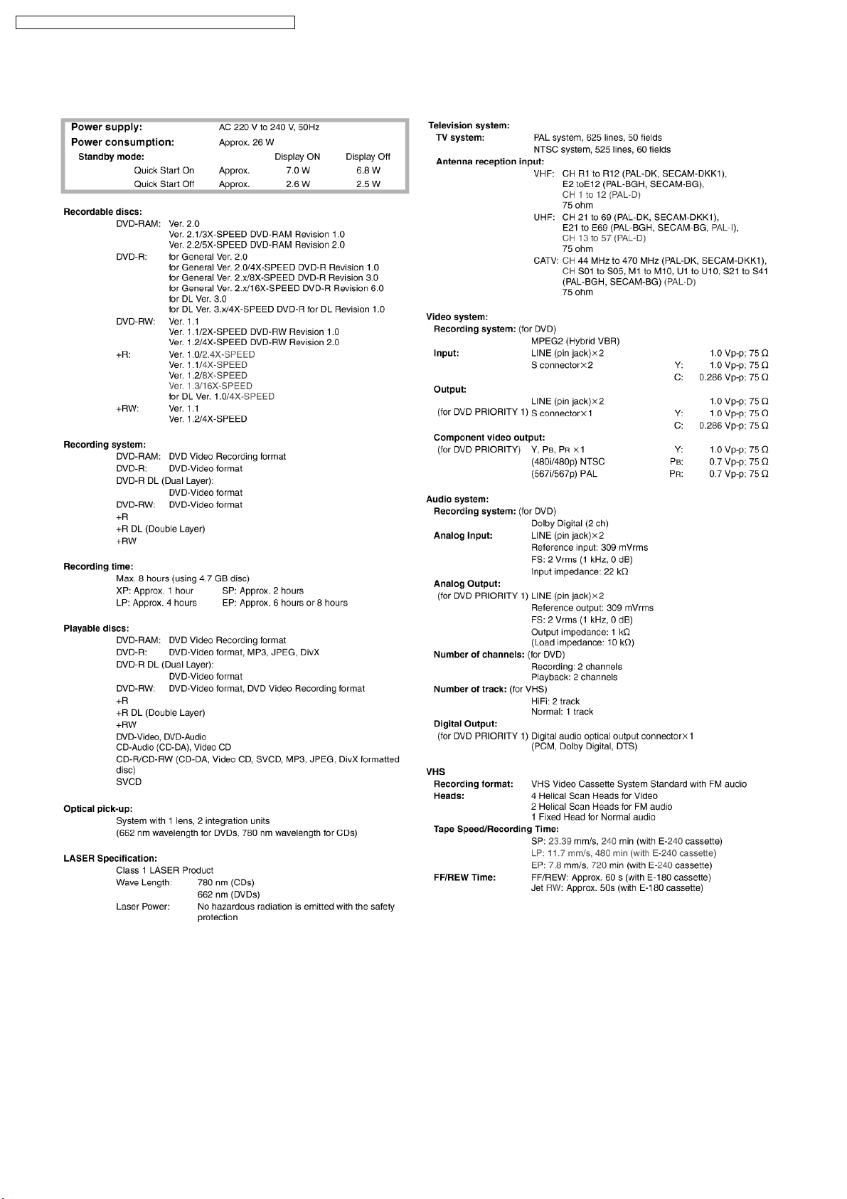
6 Specifications
(For GN/GC/GCS)
10
Page 11
DMR-ES35VGN / DMR-ES35VGC / DMR-ES35 VGCS / DMR-ES35 VEE
11
Page 12
DMR-ES35VGN / DMR-ES35VGC / DMR-ES35 VGCS / DMR-ES35 VEE
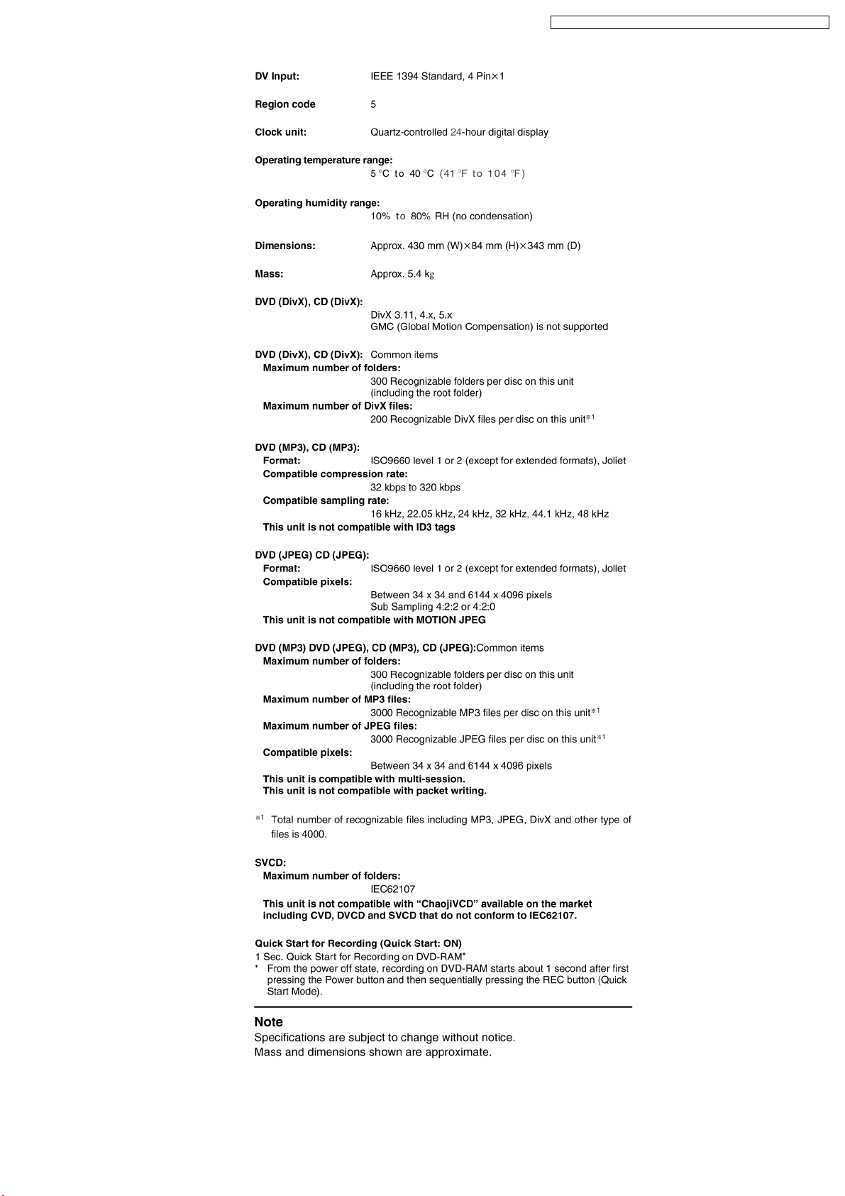
(For EE)
12
Page 13
DMR-ES35VGN / DMR-ES35VGC / DMR-ES35 VGCS / DMR-ES35 VEE
13
Page 14
DMR-ES35VGN / DMR-ES35VGC / DMR-ES35 VGCS / DMR-ES35 VEE
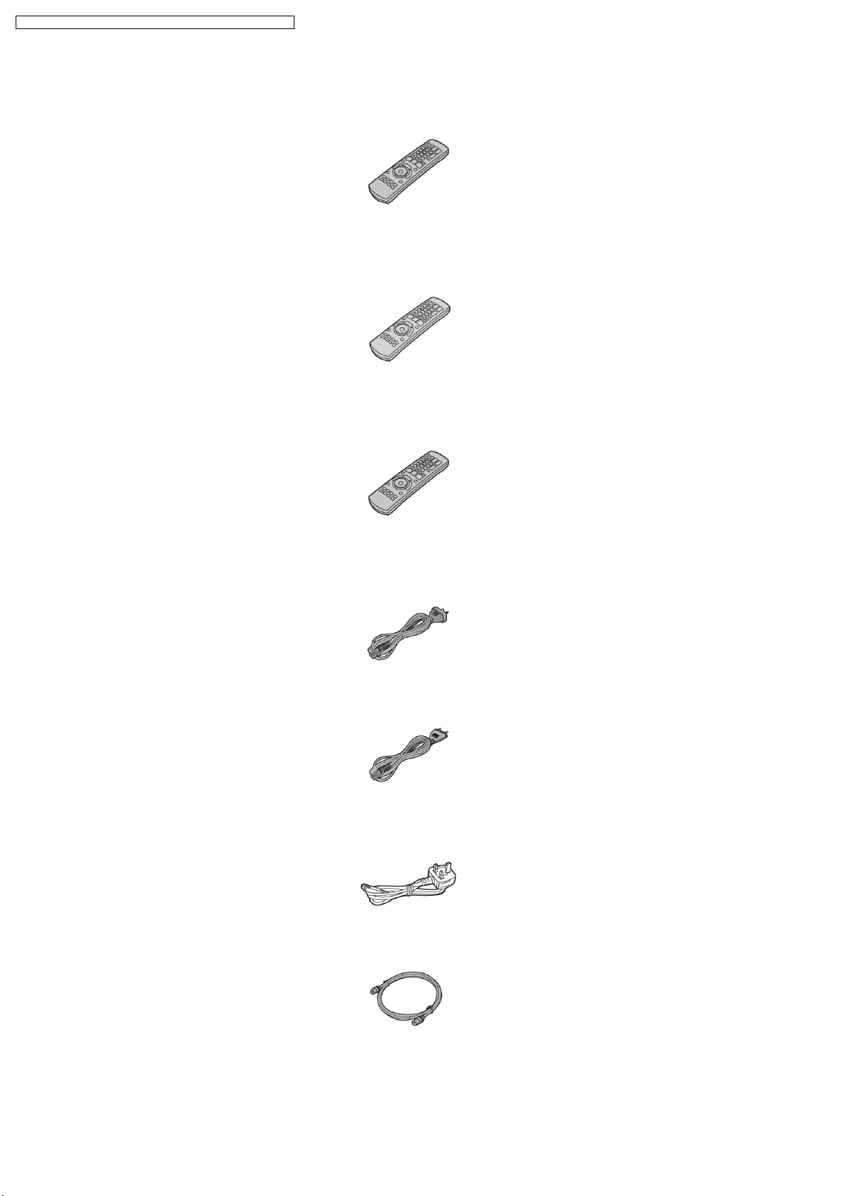
7 Accessories
Note : Refer to Replacement Parts List (Section 22) for the part number.
Remote control (For
GC/GCS)
Remote control (For
GN)
Remote control (For
EE)
AC Cord (For GN)
AC Cord (For
GC/GCS/EE)
AC Cord (For GC)
RF coaxial cable
14
Page 15

Audio/Video cable
DMR-ES35VGN / DMR-ES35VGC / DMR-ES35 VGCS / DMR-ES35 VEE
15
Page 16
DMR-ES35VGN / DMR-ES35VGC / DMR-ES35 VGCS / DMR-ES35 VEE
8 Operation Instructions Procedures
8.1. Remote Control Operation (For GN/GC/GCS)
16
Page 17
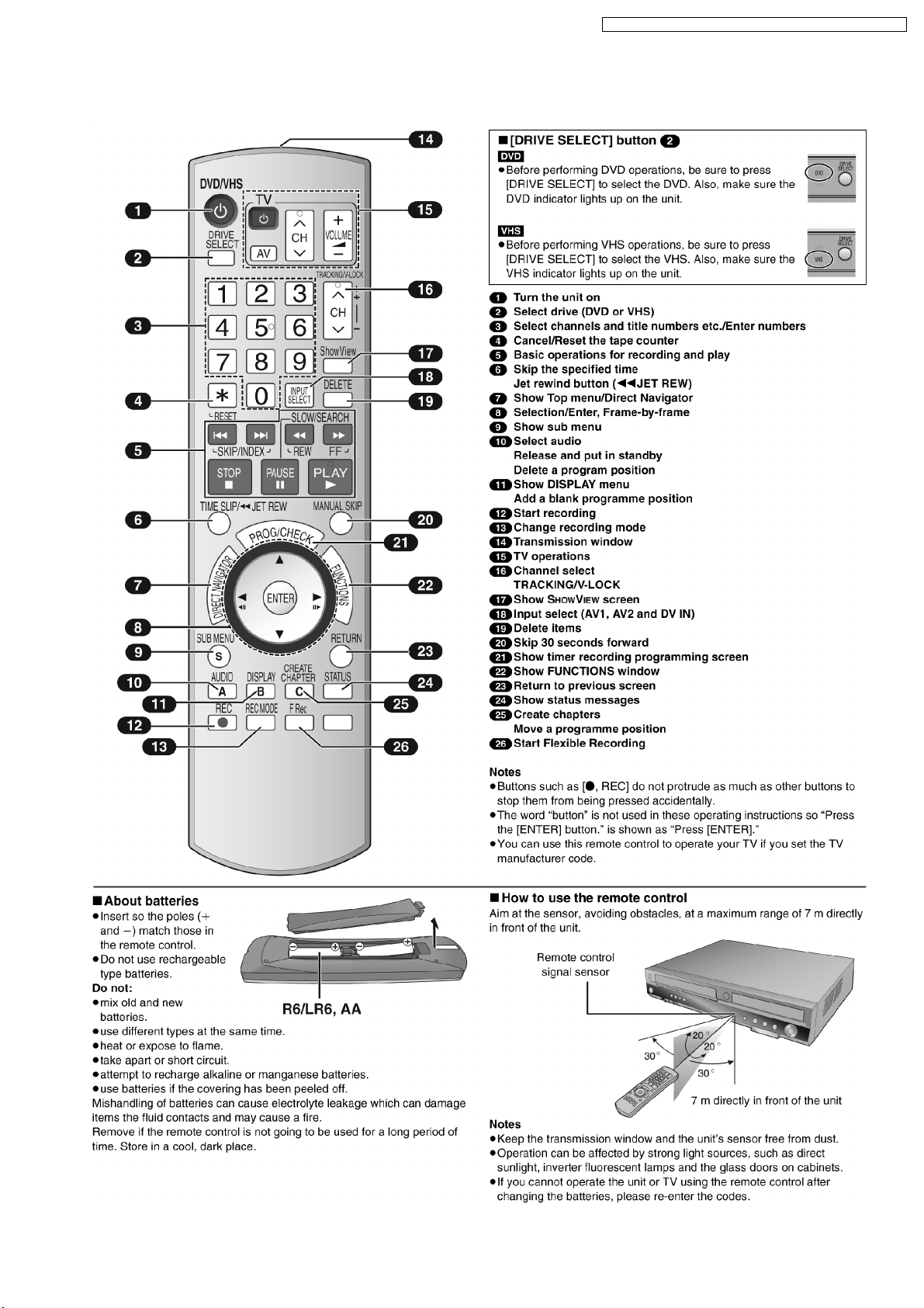
8.2. Remote Control Operation (For EE)
DMR-ES35VGN / DMR-ES35VGC / DMR-ES35 VGCS / DMR-ES35 VEE
17
Page 18
DMR-ES35VGN / DMR-ES35VGC / DMR-ES35 VGCS / DMR-ES35 VEE
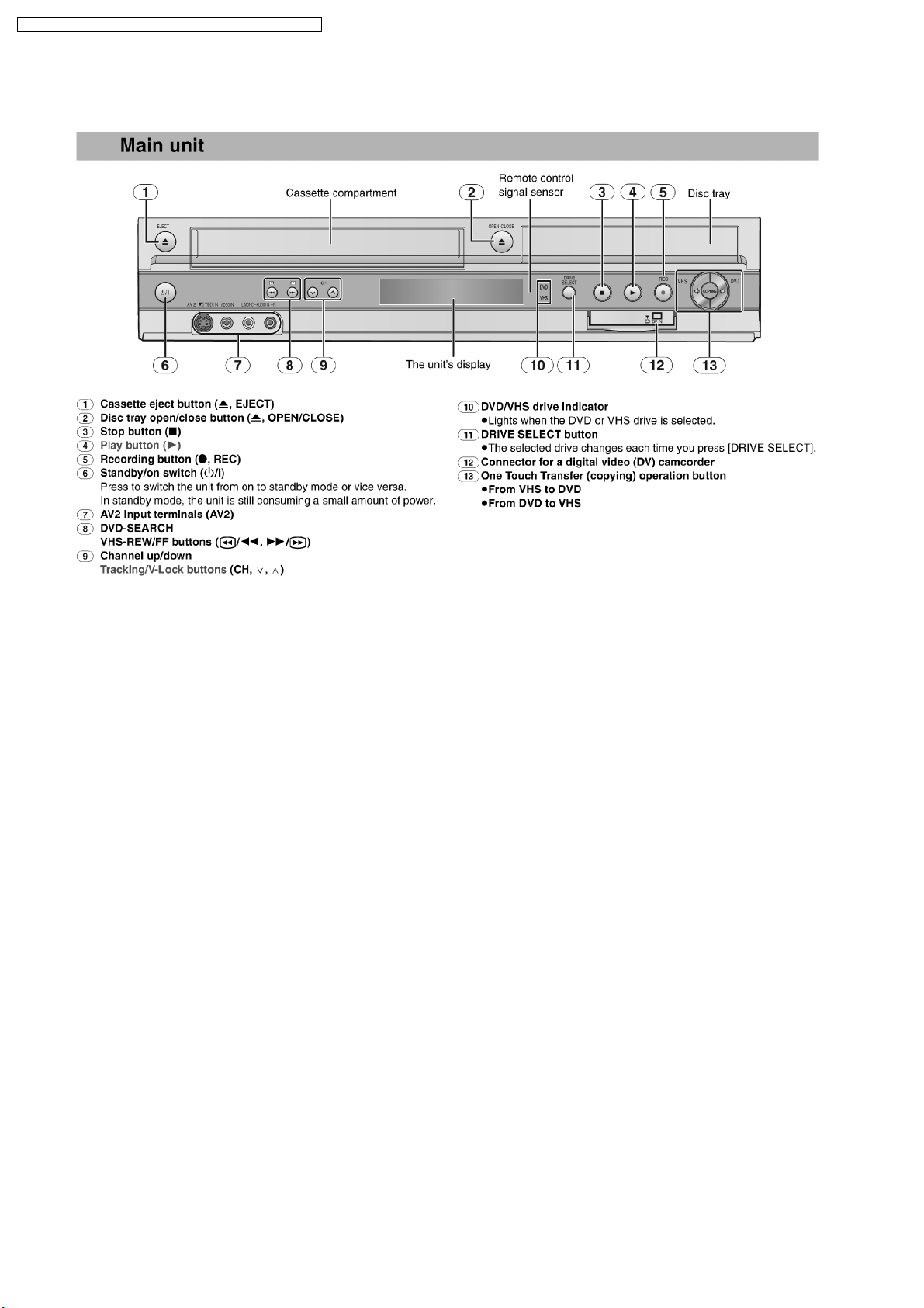
8.3. Main Unit Operation
18
Page 19
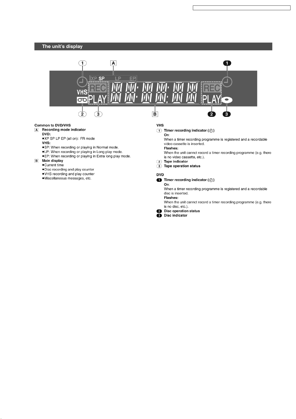
8.4. Main Unit Panel Display
DMR-ES35VGN / DMR-ES35VGC / DMR-ES35 VGCS / DMR-ES35 VEE
19
Page 20
DMR-ES35VGN / DMR-ES35VGC / DMR-ES35 VGCS / DMR-ES35 VEE
8.5. Disc Information
8.5.1. Discs for recording & play
20
Page 21
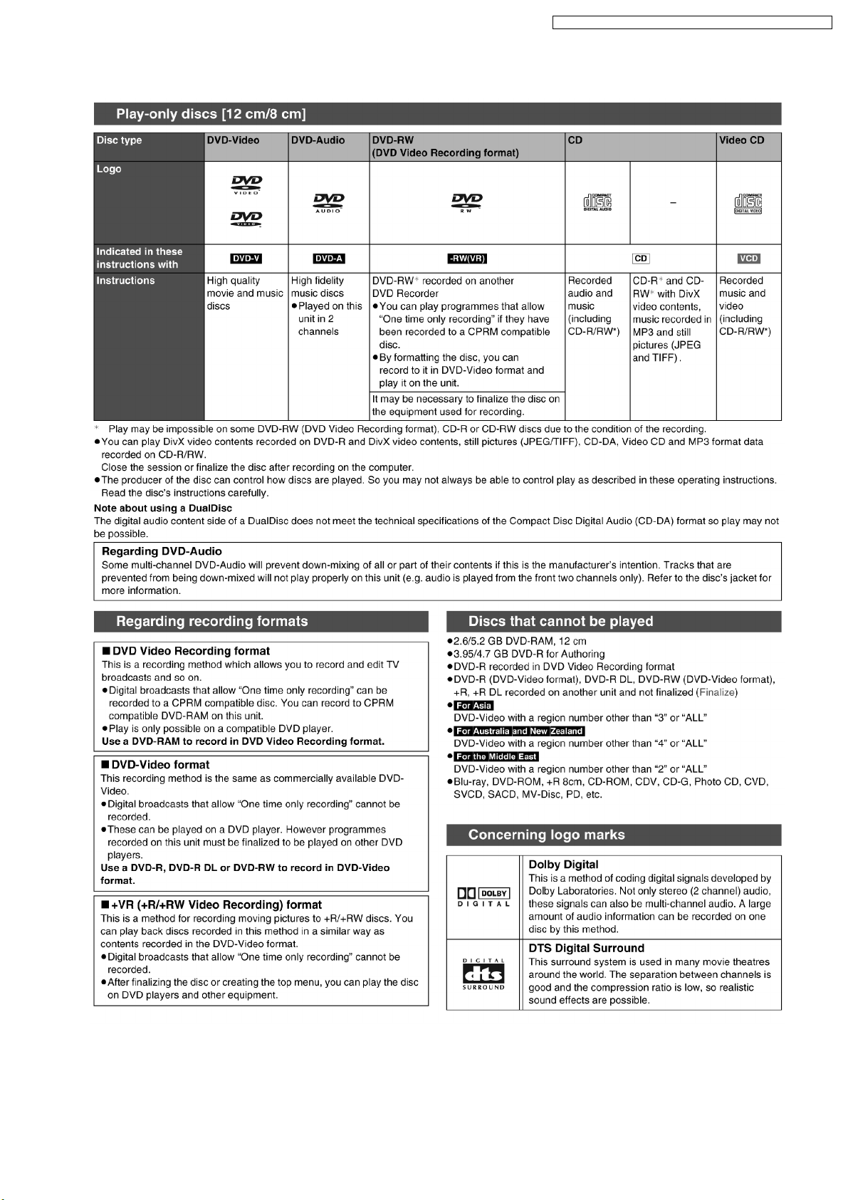
8.5.2. Discs for playing
DMR-ES35VGN / DMR-ES35VGC / DMR-ES35 VGCS / DMR-ES35 VEE
21
Page 22
DMR-ES35VGN / DMR-ES35VGC / DMR-ES35 VGCS / DMR-ES35 VEE
22
Page 23
DMR-ES35VGN / DMR-ES35VGC / DMR-ES35 VGCS / DMR-ES35 VEE
23
Page 24
DMR-ES35VGN / DMR-ES35VGC / DMR-ES35 VGCS / DMR-ES35 VEE
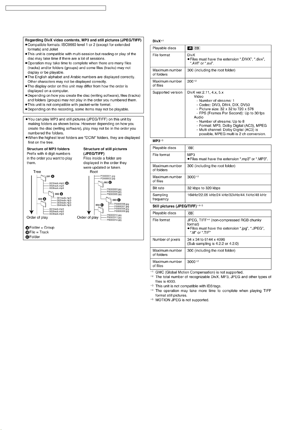
8.5.3. Data playable format (DivX, MP3, JPEG, TIFF)
24
Page 25
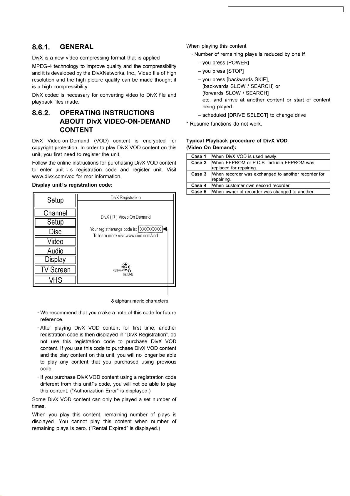
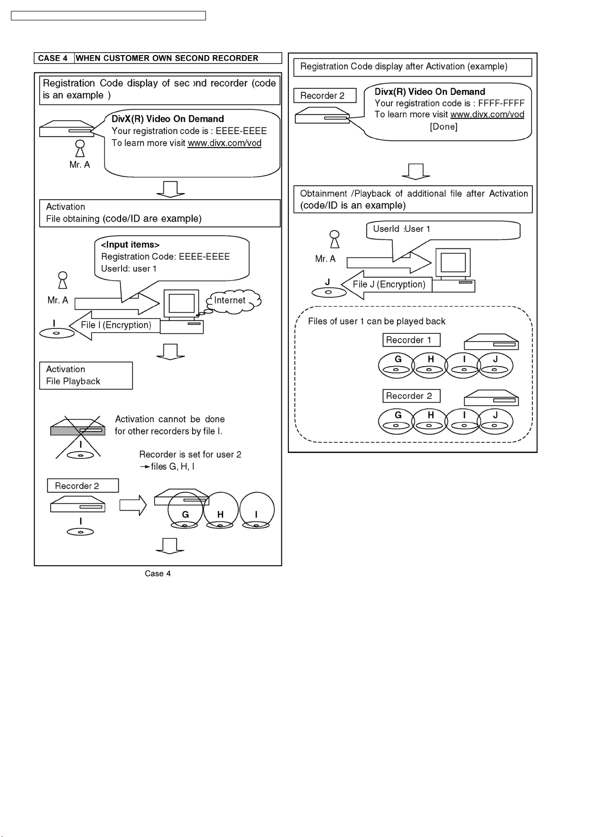
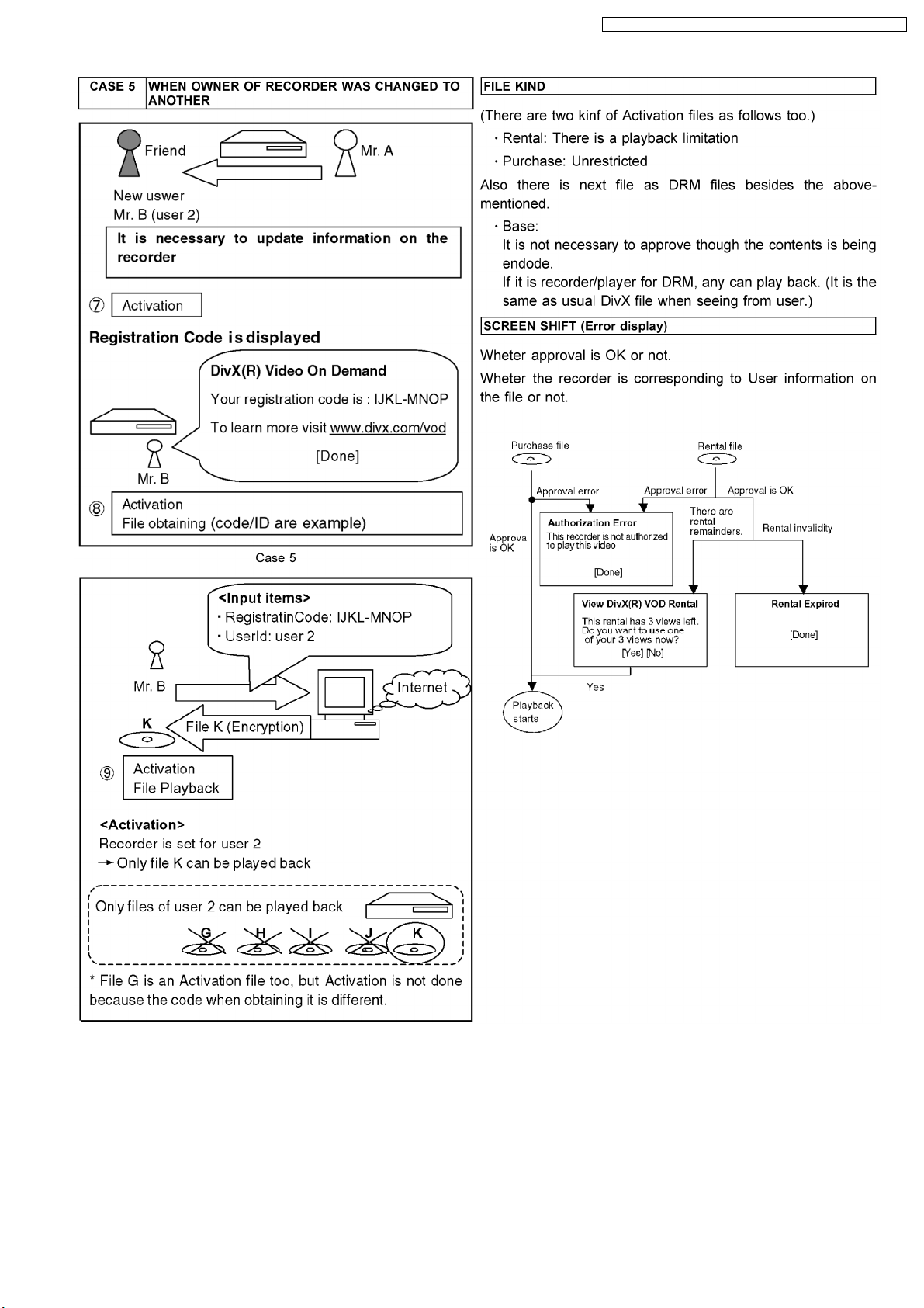
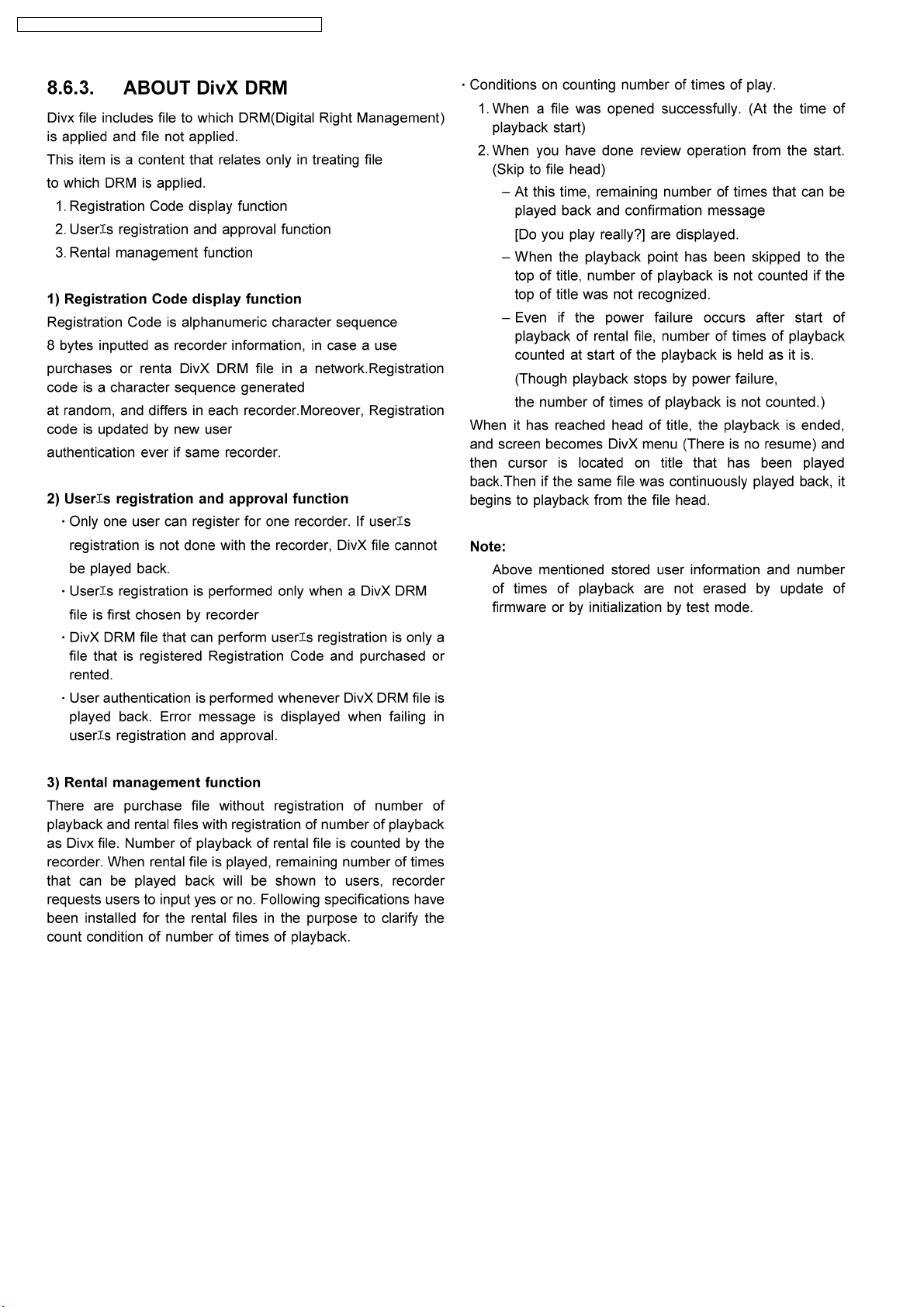
8.6. ABOUT DivX
DMR-ES35VGN / DMR-ES35VGC / DMR-ES35 VGCS / DMR-ES35 VEE
25
Page 26
DMR-ES35VGN / DMR-ES35VGC / DMR-ES35 VGCS / DMR-ES35 VEE
26
Page 27
DMR-ES35VGN / DMR-ES35VGC / DMR-ES35 VGCS / DMR-ES35 VEE
27
Page 28
DMR-ES35VGN / DMR-ES35VGC / DMR-ES35 VGCS / DMR-ES35 VEE
28
Page 29
DMR-ES35VGN / DMR-ES35VGC / DMR-ES35 VGCS / DMR-ES35 VEE
29
Page 30
DMR-ES35VGN / DMR-ES35VGC / DMR-ES35 VGCS / DMR-ES35 VEE
30
Page 31

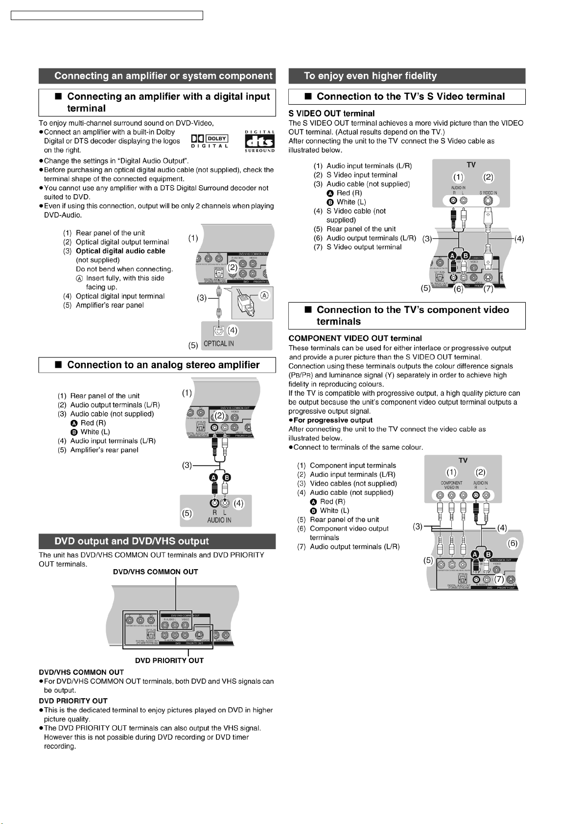
8.7. Connection to other Devices
8.7.1. Connection to TV (For GN/GC/GCS)
DMR-ES35VGN / DMR-ES35VGC / DMR-ES35 VGCS / DMR-ES35 VEE
31
Page 32

DMR-ES35VGN / DMR-ES35VGC / DMR-ES35 VGCS / DMR-ES35 VEE
8.7.2. Connection to amplifier / system component
32
Page 33

8.8. Connection to other Devices
8.8.1. Connection to TV (For EE)
DMR-ES35VGN / DMR-ES35VGC / DMR-ES35 VGCS / DMR-ES35 VEE
33
Page 34
DMR-ES35VGN / DMR-ES35VGC / DMR-ES35 VGCS / DMR-ES35 VEE
8.8.2. Connection to amplifier / system component
34
Page 35

DMR-ES35VGN / DMR-ES35VGC / DMR-ES35 VGCS / DMR-ES35 VEE
9 Operation Instructions
9.1. (DVD) Taking out the Disc from RAM-Drive Unit when the Disc cannot
be ejected by OPEN/CLOSE button
9.1.1. (DVD) Forcible Disc Eject
9.1.1.1. (DVD) When the power can be turned off.
1. Turn off the power and press [STOP], [CH UP] keys on the front panel simultaneously for 5 seconds.
9.1.1.2. (DVD) When the power can not be turned off.
1. Press [POWER] key on the front panel for over 10 seconds to turn off the power forcibly, and press [STOP] [CH UP] keys on
the front panel simultaneousl y for 5 second s.
9.1.2. (DVD) When the Forcible Disc Eject can not be done.
1. Turn off the power and pull out AC cord.
2. Remove the Top Case.
3. Push in SLIDE CAM by Eject Pin(JZS0484) or minus screw driver (small) to eject tray slightly.
4. Push out Tray by Eject Pin (JZS0484) or minus screw driver (small).
35
Page 36

DMR-ES35VGN / DMR-ES35VGC / DMR-ES35 VGCS / DMR-ES35 VEE
9.2. (VHS) Removing Cassette
Tape manually
When the cassette tape could not be uninstalled from an
electrical malfunction, there are 2 ways to remove a cassette
tape.
9.2.1. (VHS) Removal by compulsory
unloading.
If Service Mode can be activated when the power can not be
turned on, this operation is able.
1. Press [STOP] and [EJECT] button simultaneously for more
than 3 seconds and set the Service Mode to 7.
2. Press [STOP] button in order to unload the mechanism.
(Pay attention to tape slack)
Service Mode Display:
7 ** ** (STOP) → 7 0L ** (EJECT)
9.2.2. (VHS) Removal by manual
operation by rotating the Loading
Motor with the batteries.
1. Disconnect the AC plug, and remove the Top Panel and the
Front Panel by referring to the Disassembly Procedures.
2. Connect three batteries (1.5V spec.) to the Loading Motor
in series for supplying 4.5V to rotate the Loading Motor as
shown below.
3. Stop unload ing just before unloading will be completed as
shown below, and then the tape becomes slack as shown
below.
4. Rotate the S-Reel by a small minus screwdriver to remove
the slack tape as shown below.
5. Then unload again to remove the cassette tape as shown
below.
9.2.3. (VHS) Take out Cassette
Tapemanually after removing the
mechanism
1. Disconnect the AC plug, and remove the Top Case, Front
Panel and the Mechanism by referring to "12 Assembling
and Disassembling"
2. Remove the Screw and remove the Loading Motor as
shown below.
36
Page 37

3. Rotate the Main Cam Gear counter-clockwise until just
before the unloading will be completed as shown below. .
DMR-ES35VGN / DMR-ES35VGC / DMR-ES35 VGCS / DMR-ES35 VEE
4. Rotate the Capstan Motor clockwise to remove the slack
tape as shown below.
5. Rotate the Main Cam Gear counter-clockwise again to
remove the cassette-tape as shown below.
6. Attach Loading Motor and tighten the screw.
7. Set the Position Switch to EJECT POSITION certainly and
attach the mechanism to chassis as shown below.
37
Page 38

DMR-ES35VGN / DMR-ES35VGC / DMR-ES35 VGCS / DMR-ES35 VEE
10 Service Mode
10.1. (DVD) Self-Diagnosis and Special Mode Setting
10.1.1. (DVD) Self-Diagnosis Functions
Self-Diagnosis Function provides information for errors to service personnel by “Self-Diagnosis Display” when any error has
occurred.
U**, H** and F** are stored in memory and held.
You can check latest error code by transmitting [0] [1] of Remote Controller in Service Mode.
Automatic Display on FL will be cancelled when the power is turned off or AC input is turned off during self-diagnosis display is ON.
Error Code Diagnosis contents Description Monitor Display Automatic FL display
U30 Remote control code error Display appears when main unit and remote
U59 Abnormal inner temperature
detected
U61 The unit is carrying out its
recovery process.
controller codes are not matched.
Display appears when the drive temperature
exceeds 70°C.
The power is turned off forcibly.
For 30 minutes after this, all key entries are
disabled. (Fan motor operates at the highest
speed for the first 5 minutes. For the
remaining 25 minutes, fan motor is also
stopped.) The event is saved in memory as
well.
No display
“*” is remote controller code of the
main unit.
Display for 5 seconds.
No display
“U59 is displayed for 30 minutes.
No display
U88 The unit is carrying out its
U99 Hang-up Displayed when communication error has
H19 Inoperative fan motor When inoperative fan motor is detected after
F00 No error information Initial setting for error code in memory
F09 Serial Communication Error
F34 Initialization error when main
F58 Drive hardware error When drive unit error is detected, the event is
F60 DVD module has not been
recovery process.
between VHS Microprocessor
and Timer Microprocessor.
microprocessor is started up
for program recording
started.
occurred between Main microprocessor and
Timer microprocessor.
powered on, the power is turned off
automatically.
The event is saved in memory.
(Error code Initialization is possible with error
code initialization and main unit initialization.)
Please confirm Serial Communication
terminal of Microprocessor.
NOTE:
If F09 appears just after updating Firmware,
pull off and insert AC plug, then it will
disappear.
When initialization error is detected after
starting up main microprocessor for program
recording, the power is turned off
automatically.
The event is saved in memory.
saved in memory.
Defect of Digital P.C.B.
Mode: No change
No display
No display
Displayed is left until the
[POWER] key is pressed.
No display No display
No display No display
No display
No display No display
No display No display
No display
38
Page 39

DMR-ES35VGN / DMR-ES35VGC / DMR-ES35 VGCS / DMR-ES35 VEE
Error Code Diagnosis contents Description Monitor Display Automatic FL display
UNSUP-
PORT
NO READ Disc read error *A disc is flawed or dirty.
HARD
ERR
Unsupported disc error *An unsupported format disc was played,
although the drive starts normally.
*The data format is not supported, although
the media type is supported.
*Exceptionally in case of the disc is dirty.
*A poor quality failed to start.
*The track information could not be read.
Drive error The drive detected a hard error. “DVD drive error.” Display for 5 seconds.
“This disc is
incompatible.”
Display for 5 seconds.
“Cannot read.
Please check the
disc.”
SELF
CHECK
PLEASE
WAIT
UNFORMAT
IR ERR IR communication error [IR ERR] is display when communication
No REC Recording is impossible [No REC] is displayed when recording
Restoration operation Since the power cord fell out during a power
failure or operation, it is under restoration
operation.
*It will OK, if a display disappears
automatically. If a display does not disappear,
there is the possibility that defective Digital
P.C.B. / RAM drive.
Unit is in termination process Unit is in termination process now.
“BYE” is displayed and power will be turned
off.
In case “Quick Start” of setup menu is ON, it
is displayed in restoration operation for AC
off.
Unformatted disc error You have inserted an unformatte d DVD-RAM
or DVD-RW that is unformatted or recorded
on other equipment.
between Timer microprocessor and IR
microprocessor fails.
isimpossible due to the defect, dirt or woundof
media.
No display
No display
No display
No display
10.1.2. (DVD) Special Modes Setting
Item FL display Key operation
Mode name Description Front Key
TEST Mode *All the main unit´s parameters (include tuner)
are initialized.
Rating password The audiovisual level setting password is
initialized to “Level 8”.
Service Mode Setting every kind of modes for servicing.
*Details are described in “10.1.3. (DVD)
Service Modes at a glance”.
Forced disc eject Removing a disc that cannot be ejected.
The tray will open and unit will shift to P-off
mode.
*When Timer REC is ON, execute " Forced
disc eject " after releasing Timer REC.
While Demonstration Lock is being set, this
Forced disc eject function is not accepted.
The display before execution
leaves.
Press [VHS to DVD COPYING],
[REC] and [OPEN/CLOSE] keys
simultaneously for five seconds
when power is off.
Set DRIVE SELECT to [DVD].
While the tray is open, press [REC]
and [PLAY] simultaneously for 5
seconds.
When the power is off, press [VHS
to DVD COPYING], [OPEN/CLOSE]
and [STOP] keys simultaneously for
5 seconds.
When the power is off, press
[STOP] and [CH UP] keys
simultaneously for 5 seconds.
Forced power-off When the power button is not effective while
power is ON, turn off the power forcibly.
*When Timer REC is ON, execute “Forced
Power-off” after releasing Timer REC.
Display in P-off mode. Press [POWER] key over than 10
seconds.
39
Page 40

DMR-ES35VGN / DMR-ES35VGC / DMR-ES35 VGCS / DMR-ES35 VEE
Item FL display Key operation
Mode name Description Front Key
Child lock/unlock Set or release “Child Lock”. Press [ENTER] and [RETURN] by
remote controller simultaneously
until [X-HOLD] is displayed.
NTSC/PAL system select To switch PAL/NTSC altemately. The display before execution
Aging Perform sequence of modes as * Aging
Description shown below continually.
leaves.
Display following the then mode. When the power is ON, press [CH
Aging Contents (Example):
While the power is on (E-E mode),
press [STOP] and [OPEN/CLOSE]
simultaneously for 5 seconds.
DOWN], [VHS to DVD COPYING]
and [OPEN/CLOSE] simultaneously
for over 5 seconds and less than 10
seconds.
NOTE1:
If Unit has not turned into Aging
mode by operations shown above,
execute TEST MODE once and reexecute operation shown above.
(*All the main unit’s parameters
include tuner are initialized by TEST
mode.)
NOTE2:
If the unit has hung-up because of
pressing keys for over 10 seconds,
once turn off the power, and reexecute this command.
*When releasing Aging mode, press
[POWER] key.
Demonstration
lock/unlock
Progressive initialization The progressive setting is initialized to
ATP re-execution Re-execute ATP. Display at ATP executing. When the power is on (E-E mode),
Ejection of the disc is prohibited.
The lock setting is effective until unlocking the
tray and not released by “Main unit
initialization” of service mode.
Interlace.
*When lock the tray.
“LOCK” is displayed for 3 seconds.
*When unlock the tray.
“UNLOCK” is displayed for 3
seconds.
*When press OPEN/CLOSE key
while the tray being locked.
Display “LOCK” for 3 seconds.
The display before execution
leaves.
When the power is on, press
[STOP] and [POWER] keys
simultaneously for 5 seconds.
Note:
When a disc is not in tray, this
setting is not effective.
When the power is on, press
[STOP] and [POWER] keys
simultaneously for 5 seconds.
Press [OPEN/CLOSE] key while the
tray being locked.
When the power is on (E-E mode),
press [STOP] and [VHS to DVD
COPYING] simultaneously for 5
seconds.
press [CH UP] and [CH DOWN]
simultaneously for 5 seconds.
40
Page 41

DMR-ES35VGN / DMR-ES35VGC / DMR-ES35 VGCS / DMR-ES35 VEE
10.1.3. (DVD) Service Modes at a glance
Service mode setting: While the power is off, press [STOP], [VHS to DVD COPYING] and [OPEN / CLOSE] simultaneously for
five second s (OPERATION SELECT should be set to DVD).
Item FL display Key operation
Mode name Description (Remote controller key)
Release Items Item of Service Mode executing is cancelled. Press [0] [0] or [Return] in service
mode.
Error Code Display Last Error Code of U/H/F held by Timer is
displayed on FL.
*Details are described in “10.1.1. (DVD) Self-
Diagnosis Functions” .
ROM Version Display 1. Region code (displayed for 5 sec.)
2. Main firm version (displayed for 5 sec.)
3. Timer firm version (displayed for 5 sec.)
4. Drive firm version (displayed for 5 sec.)
5. ROM correction version
(displayed for 5 sec.)
6. VHS Microprocessor version
(displayed for 5 sec.)
7. VHS ROM correction version
(left displated)
White Picture Output White picture is output as component Output
from AV Decoder.
*White picture
(Saturation rate : 100%)
*It is enable to switch Interlace/P rogressive by
“I/P switch: [1] [4]”
Press [0] [1] in service mode
If any error history dose not exist,
[F00] is displayed.
Press [0] [2] in service mode
‘’’’ are version displays.
*Initial mode is “Interlace”. Press [1] [1] in service mode.
Switch Interlace/Progressive Press [1] [4] in White Picture Output
mode.
*I/P are switched alternately.
Magenta Picture Output Magenta picture is output with Component
RTSC Return in XP
(A & V)
Output from AV Decoder.
*Magenta picture
(Saturation rate: 100%)
*It is enable to switch Interlace/P rogressive by
“I/P switch: [1] [4]”
L1 input signal is encoded (XP), decoded
(XP) and output decoded signal to external
without DISC recording and DISC playback.
*Initial mode is “Interlace”. Press [1] [2] in service mode.
Switch Interlace/Progressive Press [1] [4] in Magenta Picture
Initial mode: EE2/ Interlace/ XP/
Audio 48kHz
Switch Interlace/Progressive Press [1] [4] in RTSC Return XP
Audio 44.1 kHz/ 48 kHz Switch Press [2] [4] in RTSC Return XP
Output mode.
*I/P are switched alternately.
Press [1] [3] in service mode.
mode.
*I/P are switched alternately.
mode.
*48 kHz / 44.1 kHz are switched
alternately.
41
Page 42

DMR-ES35VGN / DMR-ES35VGC / DMR-ES35 VGCS / DMR-ES35 VEE
Item FL display Key operation
Mode name Description (Remote controller key)
I/P Switch Switch Interlace and Progressive in EE mode.
*Initial setting is “Interlace”.
*This command is effective during executing
“White Picture Output”, “Magenta Picture
Output” and “RTSC Return in XP (A & V)”
modes.
Initial mode is Interlace
Switch Interlace/Progressive
Press [1] [4] in I/P Switch mode.
*I/P are switched alternately.
Audio Mute (XTMUTE) Check whether mute is applied normally by
the timer microprocessor.
Audio Mute (XDMUTE) Check whether mute is applied normally by
the Digital P.C.B..
Audio Pattern Output The audio pattern stored in the internal
memory is output
(Lch: 1kHz/-18dB)
(Rch: 400Hz/-18dB)
*Audio sound clock switching operation of
DAC can be confirmed by sub command [2]
[4].
Laser Used Time
Check laser used time (hours) of drive.
Indiction
Delete the Laser Used
Time
Laser used time stored in the memory of the
unit is deleted.
Press [2] [1] in service mode.
Press [2] [2] in service mode.
Initial mode (Audio 48kHz) Press [2] [3] in service mode.
Audio 44.1kHz/48kHz switching Press [2] [4] in Audio Pattern Output
mode.
*48 kHz / 44.1 kHz are switched
alternately.
Press [4] [1] in service mode.
l(*****) is the used time display in
hour.
lLaser used time of DVD/ CD in
Playback/Recording mode is
counted.
Press [9] [5] in service mode.
42
Page 43

DMR-ES35VGN / DMR-ES35VGC / DMR-ES35 VGCS / DMR-ES35 VEE
Item FL display Key operation
Mode name Description (Remote controller key)
RAM Drive Last Error RAM Drive error code display.
*For details about the drive error code, refer
to the Service Manual for the specific RAM
Drive.
1. Error Number is displayed for 5
seconds.
Press [4] [2] in service mode.
When “INFO******” is being
displayed, past 19 error histories
can be displayed by pressing [0] [1]
- [1] [9]
2. Time when the error has occurred
is displayed for 5 seconds.
DD: Day
hh: Hour
mm: Minute
3. Last Drive Error (1/2) is displayed
for 5 seconds.
4. Last Drive Error (2/2) is displayed
for 5 seconds.
5. Error occurring Disc type is
displayed for 5 seconds.
Delete the Last Drive
Error
Delete the Last Drive Error information stored
on the DVD RAM-Drive.
Laser power confirmation Drive state is judged based on difference
between laser power value at shipping and
present laser power value.
Turn on all FL/LEDs All segments of FL and all LEDs are turned
on.
S1 signal output Forcibly superimpose the S1 signal (approx.
4.5V DC) on the EE chroma signal, and check
the output on the S terminal.
S2 signal output Forcibly superimpose the S2 signal (approx.
2V DC) on the EE chroma signal, and check
the output on the S terminal.
AV4(V)/AV1(RGB) I/O
Setting
Set input to AV4 (V) and set output to AV1
(RGB) for I/O checking
6. Disc Maker ID is displayed for 5
seconds.
In case that the maker cannot be
identified, display is black out.
7. Factor of Drive Error occurring is
left displayed
Press [9] [6] in service mode.
1. into RAM
Drive in service mode. (Other
media are assumed to be noncorrespondence.)
2. Press [4] [4].
If DVD-RAM disc in not inserted,
[NO DISC] is displayed.
If power value study was filed,
[ERROR] is displayed.
All segments are turned on. Press [5] [1] in service mode.
Press [5] [2] in service mode.
Press [5] [3] in service mode.
Press [8] [0] in service mode.
43
Page 44

DMR-ES35VGN / DMR-ES35VGC / DMR-ES35 VGCS / DMR-ES35 VEE
Item FL display Key operation
Mode name Description (Remote controller key)
AV2(Y/C)/AV1(V)
I/OSetting
Set input to AV2 (Y/C) and set output to AV1
(V) for I/O checking
Press [8] [0] in service mode.
Front connection
inspection
Press all front keys and check the connection
between Main P.C.B. and Front key Switches.
(1) Each time a key is pressed,
segment turned on increases one
by one.
(2) Total umber of keys that have
been pressed.
Production Date Display Display the date when the unit was produced.
YY: Year
MM: Month
DD: Day
Display the accumlated
Display the accumulated unit´s working time.
working time
(Indicating unit: Second)
Display the Error History Display the Error History stored on the unit. Display reason of error for 5
seconds.
01:
Defect of Digital P.C.B.
(AV DEC / MAIN CPU)
02:
Defect of RAM Drive.
03:
Defect of Disc.
04:
Defect of Digital P.C.B. or
Communication Error.
05:
Defect of Digital P.C.B.
(AV DEC / MAIN CPU)
Press [5] [4] in service mode.
Press [6] [1] in service mode.
Press [6] [4] in service mode.
Press [6] [5] in service mode.
Then press [0] [1] ~ [1] [9], the past
19 error histories are displayed.
Delete the Error History Delete Error History information stored on the
unit.
Tray OPEN/CLO SE Test The RAM drive tray is opened and closed
repeatedly.
Error code initialization Initialization of the last error code held by
timer (Write in F00)
Display the time when the error has
occurred for 5 seconds.
DD: Day
hh: Hour
mm: Minute
Accumulated working time till
occuring of the error is left
displayed.
(Indicating unit: Second)
“*” is number of open/close cycle
times.
Press [9] [7] in service mode.
Press [9] [1] in service mode
*When releasing this mode, press
the [POWER] button of Remote
Controller more than 10 seconds.
Press [9] [8] in service mode.
44
Page 45

DMR-ES35VGN / DMR-ES35VGC / DMR-ES35 VGCS / DMR-ES35 VEE
Item FL display Key operation
Mode name Description (Remote controller key)
Initialize Service Last Drive Error, Error history and Error
Press [9] [9] in service mode.
Codes stored on the unit are initialized to
factory setting.
PB HIGH Signal Output 8 pin of AV 1 Jack (PB HIGH terminal) is High
Press [5] [2] in service mode.
(approx. 11V DC).
PB MIDDLE Signal
Output
8 pin of AV 1 Jack (PB HIGH terminal) is
Middle (approx. 5.5V DC)
Press [5] [3] in service mode.
Finishing service mode Release Service Mode. Display in STOP (E-E) mode. Press power button on the front
panel or Remote controller in
service mode.
AV2(V)/AV1(Y/C) I/O
Setting
AV2(RGB)/AV1(V)
I/OSetting
P50(H) Output Timer Microprocessor IC7504-76 output High
Set input to AV2 (V) and set output to AV1
(Y/C) for I/O checking
Set input to AV2 (RGB) and set output to AV1
(V) for I/O checking
When OK.
Press [8] [2] in service mode.
Press [8] [3] in service mode.
Press [8] [4] in service mode.
signal for AV1-pin 10 passing through inverter
(approx. 0V DC at AV1-pin 10).
When NG.
P50(L) Output Timer Microprocessor IC7504-76 output Low
When OK.
Press [8] [5] in service mode.
signal for AV1-pin 10 passing through inverter
(approx. 4.4V DC at AV1-pin 10).
When NG.
Tray OPEN/CLO SE Test The RAM drive tray is opened and closed
repeatedly.
Press [9] [1] in service mode*When
releasing this mode, press the
[POWER] button of Remote
“*” is number of open/close cycle
Controller more than 10 seconds.
times.
Error code initialization Initialization of the last error code held by
Press [9] [8] in service mode.
timer (Write in F00)
Initialize Service Last Drive Error, Error history and Error
Press [9] [9] in service mode.
Codes stored on the unit are initialized to
factory setting.
Finishing service mode Release Service Mode. Display in STOP (E-E) mode. Press power button on the front
panel or Remote controller in
service mode.
45
Page 46

DMR-ES35VGN / DMR-ES35VGC / DMR-ES35 VGCS / DMR-ES35 VEE
10.2. (VHS) Self-Diagnosis and Special Mode Setting
10.2.1. (VHS) SPECIAL MODES SETTING
10.2.2. (VHS) SERVICE MODES
46
Page 47

DMR-ES35VGN / DMR-ES35VGC / DMR-ES35 VGCS / DMR-ES35 VEE
10.2.3. (VHS) SELF-DIAGNOSIS FUNCTIONS
This model has a self-diagnosis. If the VHS section detects trouble during installation or during use, the power is
automaticallyturned off or become power-save mode and it is memorized into the EEPROM (IC37501) as error code of two-digit
number. It ismemorized error code can be display ed in "second" display portion (the last 2 digits of the FIP) by placing the unit is
Service ModeNumber 2 when turning on the Service Information Display as for example "01" or "02" etc. as below. If a second error
occurs, themost recent error will be memorized and can be displayed in Service Mode Number 2. It can be memorized until 3 selfdiagnosishistories in maximum.In order to erase the memorized error code, press STOP and EJECT buttons on the Front Panel
simultaneously over 5 secondsduring turning on Service Information Display mode.
10.2.3.1. MEMORY OF THE SELF-DIAGNOSIS HISTORY
*This is effective only in Service Mode 3, 4, 5.
10.2.3.1.1. ERROR NUMBERS AT A GLANCE
10.2.3.1.2. MEMORY FOR THE SELF-DIAGNOSIS HISTORY
3. The self-diagnosis result is memorized the state of the moment of detecting.
4. There are the histories from number 1 to number 3.
5. The latest error is memorized on history number 1, and then the old histories are shifted to the history number 2 and 3.The error
code memorized in the history number 2 and 3 is over-written by shift.
6. If the latest error is the same with the history number 1 (2nd-latest), it is not memorized.(The same error code is not memorized
47
Page 48

DMR-ES35VGN / DMR-ES35VGC / DMR-ES35 VGCS / DMR-ES35 VEE
in succession)
10.2.3.1.3. CLEAR FOR THE SELF-DIAGNOSIS HISTORY
1. Press STOP and EJECT buttons simultaneously over 5 seconds during turning on Service Information Display mode.
10.2.3.1.4. INDICATION OF THE SELF-DIAGNOSIS HISTORY
The self-diagnosis histories can be indicated on the FIP with Service Mode number 3 to 5.
The procedure of service mode setting and indication format are the same as usual.
48
Page 49

DMR-ES35VGN / DMR-ES35VGC / DMR-ES35 VGCS / DMR-ES35 VEE
11 Service Fixture & Tools
(For DVD)
Part Number Description Compatibility
RFKZ0168 Extension Cable (Digital I/F P.C.B. - FAN / 3 Pin) Same as E50 / ES30V Series
RFKZ0327 Extension Cable (Main P.C.B. - Digital I/F P.C.B. / 15 Pin / 40 mm)
RFKZ0240 Extension Cable (Main P.C.B. - Digital I/F P.C.B. / 19 Pin / 40 mm) Same as ES75V / ES30V Series
RFKZ0368 Extension Cable (Main P.C.B. - Digital I/F P.C.B. / 11 Pin / 40 mm) New
RFKZ0239 Extension Cable (Main P.C.B. - Panel P.C.B. / 12 Pin) Same as E75V / ES30V Series
RFKZ0239 Extension Cable (Main P.C.B. - Front Jack P.C.B. / 10 Pin) Same as E75V / ES30V Series
RFKZ0365 Extension Cable (Main P.C.B. - RAM / Digital P.C.B. Module / 64 Pin) Same as ES15 Series
JZS0484 Eject Pin Same as ES15 / E50 Series
RFKZ03D01K Lead Free Solder (0.3mm/10 0g Reel) Same as ES15 Series
RFKZ06D01K Lead Free Solder (0.6mm/10 0g Reel) Same as ES15 Series
RFKZ10D01 Lead Free Solder (1.0mm/10 0g Reel)) Same as ES15 Series
RFKZ0316 Solder Remover (Lead free 10W temperature Solder/180g) Same as ES15 Series
RFKZ0328 Flux Same as ES15 Series
RFKZ0329 Bottle of Flux Same as ES15 Series
(For VHS)
Part Number Description Compatibility
VFJ8125H3F NTSC VHS Alignment Tape Same as E75V / ES30V
VFK0329 Post Adjustment Screwdriver Same as E75V / ES30V
VFK0330 Fine Adjustment Gear Driver Same as E75V / ES30V
49
Page 50

DMR-ES35VGN / DMR-ES35VGC / DMR-ES35 VGCS / DMR-ES35 VEE
12 Assembling and Disassembling
12.1. Caution
“ATTENTION SERVICER”
Some chassis components may be have sharp edges. Be careful when disassembling and servicing.
1. This section describes procedures for checking the operation of the major printed circuit boards and replacing the main
components.
2. For reassembly after operation checks or replacement, reverse the respective procedures.
Special reassembly procedures are described only when required.
3. Select items from the following index when checks or replacement are required.
4. Refer to the Parts No. on the page of “Replacement Parts List” (Section 22), if necessary.
Below is the list of disassembly sections
· Disasse mbly of Top Panel
· Disasse mbly of Nicam Decoder P.C.B.
· Disasse mbly of Front Panel
· Disasse mbly of Panel P.C.B. & Front Jack P.C.B.
· Disasse mbly of RAM/Digital P.C.B. module
· Disasse mbly of DV Jack P.C.B.
· Disasse mbly of VTR Mechanism Unit
· Disasse mbly of Rear Panel
· Disasse mbly of Fan Motor
· Disasse mbly of Digital I/F P.C.B.
· Disasse mbly of Main P.C.B.
50
Page 51

DMR-ES35VGN / DMR-ES35VGC / DMR-ES35 VGCS / DMR-ES35 VEE
12.2. Disassembly Flow Chart
The following chart is the procedure for disassembling the casing and inside parts for internal inspection when carrying out the
servicing.
To assemble the unit, reverse the steps shown in the chart below.
51
Page 52

DMR-ES35VGN / DMR-ES35VGC / DMR-ES35 VGCS / DMR-ES35 VEE
12.3. Main Parts Location Diagram
52
Page 53

DMR-ES35VGN / DMR-ES35VGC / DMR-ES35 VGCS / DMR-ES35 VEE
12.4. Caution with inserting cassette tape when disassembling the unit
Note1:
For description of the disassembling procedure, see the section 12.5.
Note2:
Video Cassette might not enter when a strong lighting is applied to VHS Mechanism when Video Cassette is inserted. Please
weaken the lighting or cover with the top panel etc.
53
Page 54

DMR-ES35VGN / DMR-ES35VGC / DMR-ES35 VGCS / DMR-ES35 VEE
12.5. Disassembly of Top Panel
Step 1 : Remove 4 Screws (A) and 3 Screws (B).
Step 2 : Slide Top Panel rearward and open the both ends at
rear side of the Top Panel a little and lift the Top Panel in the
direction of the arrows.
12.6. Disassembly of Nicam
Decoder P.C.B.
· Follow the (step 1) - (step 2) of item 12.5.
Step 1 : Disconnect 2 connectors to remove Nicam Decoder
P.C.B. as arrow shown.
54
Page 55

12.7. Disassembly of Front Panel
· Follow the (step 1) - (step 2) of item 12.5.
Step 1 : Remove 1 screw (A).
Step 2 : Unlock tab (A) and tab (B) simultaneously.
Step 3 : Unlock tab (C) and tab (D) simultaneously.
Step 4 : Unlock 2 tabs (E) respectively, and pull out Front Panel
with connector slightly.
DMR-ES35VGN / DMR-ES35VGC / DMR-ES35 VGCS / DMR-ES35 VEE
Note:
When attaching Front Panel, in order to hook Cassette
Door Opener Lever to Cassette Door, push up cassette
door in the direction of arrow and insert a front panel.
12.8. Disassembly of Front Jack
P.C.B. & Panel P.C.B.
· Follow the (step 1) - (step 2) of item 12.5.
· Follow the (step 1) - (step 4) of item 12.7.
Step 1 : Remove 6 screws (A) to remove Panel P.C.B.
Step 2 : Remove 3 screws (B) and unlock Locking Tab (A) to
remove Front Jack P.C.B.
55
Page 56

DMR-ES35VGN / DMR-ES35VGC / DMR-ES35 VGCS / DMR-ES35 VEE
12.9. Disassembly of RAM / Digital
P.C.B. Module
· Follow the (step 1) - (step 2) of item 12.5.
· Follow the (step 1) - (step 4) of item 12.7.
Step 1 : Remove 3 Screws (A).
Note: Handle the RAM Drive with care. Please put on antistatic strap when handling the drive unit
Step 2 : With holding RAM drive as below illustration, remove
3 screws (B) and disconnect FFC.
And lift up Digital P.C.B. slightly so to disconnect connectors to
remove Digital P.C.B..
Step 3 : Place the Digital P.C.B. on RAM Drive and remove
RAM/Digital P.C.B. Module.
Note:
RAM/Digital P.C.B. Module as service part has no heat sink
unit.
Before returning to customer, heat sink unit should be
installed on Digital P.C.B..
56
Page 57

DMR-ES35VGN / DMR-ES35VGC / DMR-ES35 VGCS / DMR-ES35 VEE
12.10. Disassembly of DV Jack
P.C.B.
· Follow the (step 1) - (step 2) of item 12.5.
· Follow the (step 1) - (step 4) of item 12.7.
· Follow the (step 1) - (step 2) of item 12.9.
Step 1 : Remove 7 Screws (A).
Step 2 : Remove DV Jack P.C.B. with Digital Angle.
57
Page 58

DMR-ES35VGN / DMR-ES35VGC / DMR-ES35 VGCS / DMR-ES35 VEE
12.11. Disassembly of VTR
Mechanism Unit
· Follow the (step 1) - (step 2) of item 12.5.
· Follow the (step 1) - (step 4) of item 12.7.
Step 1 : Disconnect 3 Connectors (P1531, P2501 and P4002).
Step 2 : Remove 3 Black Screws (A), Screw (B) , Screw (C)
and Screw (D).
Step 3 : Lift up VTR Mechanism Unit perpendicularly so to
disconnect Connectors (P2571 and P3001).
Note:
Pay attention to stiff connections of P2571 and P3001,
when removing VTR Mechanism Unit.
12.11.1. Caution for attaching VTR
Mechanism Unit
Step 1 : Attach VTR Mechanism Unit so that Boss of Position
SW is put into long hole of Main Cam Gear, refer to Fig. (B).
58
Page 59

DMR-ES35VGN / DMR-ES35VGC / DMR-ES35 VGCS / DMR-ES35 VEE
12.12. Disassembly of Rear Panel
· Follow the (step 1) - (step 2) of item 12.5.
Step 1 : Disconnect Fan Connector.
Step 2 : Remove 6 Screws (A) and 1 Screw (B).
Step 3 : Unlock 2 Locking Tabs (A) to remove panel Cabinet
with Fan Motor.
12.14. Disassembly of Digital I/F
P.C.B.
· Follow the (step 1) - (step 2) of item 12.5.
· Follow the (step 1) - (step 4) of item 12.7.
· Follow the (step 1) - (step 2) of item 12.9.
· Follow the (step 1) - (step 2) of item 12.10.
· Follow the (step 1) - (step 3) of item 12.12.
Step 1 : Disconnect 5 Connectors (A).
Step 2 : Remove the 2 Screws (A).
Step 3 : Remove Digital I/F P.C.B.
12.13. Disassembly of Fan Motor
· Follow the (step 1) - (step 2) of item 12.5.
Step 1 : Disconnect Fan Connector.
Step 2 : Remove 2 Screws (A) to Remove Fan Motor.
59
Page 60

DMR-ES35VGN / DMR-ES35VGC / DMR-ES35 VGCS / DMR-ES35 VEE
12.15. Main P.C.B.
· Follow the (step 1) - (step 2) of item 12.5.
· Follow the (step 1) - (step 4) of item 12.7.
· Follow the (step 1) - (step 3) of item 12.11.
· Follow the (step 1) - (step 3) of item 12.12.
Step 1 : Disconnect 5 Conne ctors.
Step 2 : Remove 2 Screws (A) and remove Main P.C.B.
60
Page 61

DMR-ES35VGN / DMR-ES35VGC / DMR-ES35 VGCS / DMR-ES35 VEE
13 Measurements and Adjustments
13.1. Service Positions
Note:
For description of the disassembling procedure, see the section 12.
13.1.1. Checking and Repairing of RAM / Digital P.C.B. Module
61
Page 62

DMR-ES35VGN / DMR-ES35VGC / DMR-ES35 VGCS / DMR-ES35 VEE
13.1.2. Checking and Repairing of Panel, Front Jack and Digital I/F P.C.B.
62
Page 63

13.1.3. Checking and Repairing of Main P.C.B.
DMR-ES35VGN / DMR-ES35VGC / DMR-ES35 VGCS / DMR-ES35 VEE
63
Page 64

DMR-ES35VGN / DMR-ES35VGC / DMR-ES35 VGCS / DMR-ES35 VEE
13.2. Caution for Replacing Parts
13.2.1. Notice for replacing parts of VHS Mechanism
13.2.1.1. Regarding change of parts of VHS mechanism
64
Page 65

13.2.2. Notice for Replacing Capstan Motor
DMR-ES35VGN / DMR-ES35VGC / DMR-ES35 VGCS / DMR-ES35 VEE
65
Page 66

DMR-ES35VGN / DMR-ES35VGC / DMR-ES35 VGCS / DMR-ES35 VEE
13.2.3. Items that should be done after replacing parts
66
Page 67

DMR-ES35VGN / DMR-ES35VGC / DMR-ES35 VGCS / DMR-ES35 VEE
67
Page 68

DMR-ES35VGN / DMR-ES35VGC / DMR-ES35 VGCS / DMR-ES35 VEE
68
Page 69

DMR-ES35VGN / DMR-ES35VGC / DMR-ES35 VGCS / DMR-ES35 VEE
13.3. Standard Inspection Specifications after Making Repairs
After making repairs, we recommend performing the following inspection, to check normal operation.
No. Procedure Item to Check
1 Turn on the power, and confirm items pointed out. Items pointed out should reappear.
69
Page 70

DMR-ES35VGN / DMR-ES35VGC / DMR-ES35 VGCS / DMR-ES35 VEE
No. Procedure Item to Check
2 Insert RAM disc. The Panasonic RAM disc should be recognized.
3 Enter the EE (TU IN / AV IN - AV OUT) mode. No abnormality should be seen in the picture, sound or operation.
4 Perform auto recording and playback for one minute using the RAM
disc.
No abnormality should be seen in the picture, sound or operation.
*Panasonic DVD-RAM disc should be used when recording and
playback.
5 If a problem is caused by a VCD, DVD-R, DVD-Video, Audio-CD, or
No abnormality should be seen in the picture, sound or operation.
MP3, playback the test disc.
6 Models with DV Input Jack: In case of that the trouble is caused by
DV terminal.
7 After checking and making repairs, upgrade the firmware to the
Models with DV Input Jack;
1) DV terminal: Check to be able to record from DVC.
Make sure that [UPDOK] appears in the FL display.
latest version.
8 Transfer [9][9] in the service mode setting, and initialize the service
settings (return various settings and error information to their
Make sure that [CLR] appears in the FL display.
After checking it, turn the power off.
default values. The laser time is not included in this initialization).
Use the following checklist to establish the judgement criteria for the picture and sound.
Item Contents Check Item Contents Check
Picture
Block noise
Crosscut noise Noise (static, background noise, etc.)
Dot noise The sound level is too low.
Picture disruption The sound level is too high.
Sound
Not bright enough The sound level changes.
Too bright
Flickering color
Color fading
Distorted sound
70
Page 71

DMR-ES35VGN / DMR-ES35VGC / DMR-ES35 VGCS / DMR-ES35 VEE
14 Miscellaneous
14.1. Abbreviations
14.1.1. DVD
INITIAL/LOGO ABBREVIATIONS
A A0~UP
ACLK
AD0~UP
ADATA
ALE
AMUTE
AREQ
ARF
ASI
ASO
ASYNC
B BCK
BCKIN
BDO
BLKCK
BOTTOM
BYP
BYTCK
C CAV
CBDO
CD
CDSCK
CDSRDATA
CDRF
CDV
CHNDATA
CKSL
CLV
COFTR
CPA
CPCS
CPDT
CPUADR
CPUADT
CPUIRQ
CPRD
CPWR
CS
CSYNCIN
CSYNCOUT
D DACCK
DEEMP
DEMPH
DIG0~UP
DIN
DMSRCK
DMUTE
DO
DOUT0~UP
DRF
DRPOUT
DREQ
DRESP
DSC
DSLF
DVD
ADDRESS
AUDIO CLOCK
ADDRESS BUS
AUDIO PES PACKET DATA
ADDRESS LATCH ENABLE
AUDIO MUTE
AUDIO PES PACKET REQUEST
AUDIO RF
SERVO AMP INVERTED INPUT
SERVO AMP OUTPUT
AUDIO WORD DISTINCTION SYNC
BIT CLOCK (PCM)
BIT CLOCK INPUT
BLACK DROP OUT
SUB CODE BLOCK CLOCK
CAP. FOR BOTTOM HOLD
BYPATH
BYTE CLOCK
CONSTANT ANGULAR VELOCITY
CAP. BLACK DROP OUT
COMPACT DISC
CD SERIAL DATA CLOCK
CD SERIAL DATA
CD RF (EFM) SIGNAL
COMPACT DISC-VIDEO
CHANNEL DATA
SYSTEM CLOCK SELECT
CONSTANT LINEAR VELOCITY
CAP. OFF TRACK
CPU ADDRESS
CPU CHIP SELECT
CPU DATA
CPU ADDRESS LATCH
CPU ADDRESS DATA BUS
CPU INTERRUPT REQUEST
CPU READ ENABLE
CPU WRITE ENABLE
CHIP SELECT
COMPOSITE SYNC IN
COMPOSITE SYNC OUT
D/A CONVERTER CLOCK
DEEMPHASIS BIT ON/OFF
DEEMPHASIS SWITCHING
FL DIGIT OUTPUT
DATA INPUT
DM SERIAL DATA READ CLOCK
DIGITAL MUTE CONTROL
DROP OUT
DATA OUTPUT
DATA SLICE RF (BIAS)
DROP OUT SIGNAL
DATA REQUEST
DATA RESPONSE
DIGITAL SERVO CONTROLLER
DATA SLICE LOOP FILTER
DIGITAL VIDEO DISC
INITIAL/LOGO ABBREVIATIONS
E EC
ECR
ENCSEL
ETMCLK
ETSCLK
F FBAL
FCLK
FE
FFI
FEO
FG
FSC
FSCK
G GND COMMON GROUNDING (EARTH)
H HA0~UP
HD0~UP
HINT
HRXW
I IECOUT
IPFRAG
IREF
ISEL
L LDON
LPC
LRCK
M MA0~UP
MCK
MCKI
MCLK
MDATA
MDQ0~UP
MDQM
MLD
MPEG
O ODC
OFTR
OSCI
OSCO
OSD
P P1~UP
PCD
PCK
PDVD
PEAK
PLLCLK
PLLOK
PWMCTL
PWMDA
PWMOA, B
ERROR TORQUE CONTROL
ERROR TORQUE CONTROL
REFERENCE
ENCODER SELECT
EXTERNAL M CLOCK (81MHz/40.5MHz)
EXTERNAL S CLOCK (54MHz)
FOCUS BALANCE
FRAME CLOCK
FOCUS ERROR
FOCUS ERROR AMP INVERTED INPUT
FOCUS ERROR AMP OUTPUT
FREQUENCY GENERAT OR
FREQUENCY SUB CARRIER
FS (384 OVER SAMPLING) CLOCK
HOST ADDRESS
HOST DATA
HOST INTERRUP T
HOST READ/WRITE
IEC958 FORMAT DATA OUTPUT
INTERPOLATION FLAG
I (CURRENT) REFERENCE
INTERFACE MODE SELECT
LASER DIODE CONTROL
LASER POWER CONTROL
L CH/R CH DISTINCTION CLOCK
MEMORY ADDRESS
MEMORY CLOCK
MEMORY CLOCK INPUT
MEMORY SERIAL COMMAND CLOCK
MEMORY SERIAL COMMAND DATA
MEMORY DATA INPUT/OUTPUT
MEMORY DATA I/O MASK
MEMORY SERIAL COMMAND LOAD
MOVING PICTURE EXPERTS GROUP
OPTICAL DISC CONTROLLER
OFF TRACKING
OSCILLATOR INPUT
OSCILLATOR OUTPUT
ON SCREEN DISPLAY
PORT
CD TRACKING PHASE DIFFERENCE
PLL CLOCK
DVD TRACKING PHASE DIFFERENCE
CAP. FOR PEAK HOLD
CHANNEL PLL CLOCK
PLL LOCK
PWM OUTPUT CONTROL
PULSE WAVE MOTOR DRIVE A
PULSE WAVE MOTOR OUT A, B
71
Page 72

DMR-ES35VGN / DMR-ES35VGC / DMR-ES35 VGCS / DMR-ES35 VEE
INITIAL/LOGO ABBREVIATIONS
R RE
RFENV
RFO
RS
RSEL
RST
RSV
S SBI0, 1
SBO0
SBT0, 1
SCK
SCKR
SCL
SCLK
SDA
SEG0~UP
SELCLK
SEN
SIN1, 2
SOUT1, 2
SPDI
SPDO
SPEN
SPRCLK
SPWCLK
SQCK
SQCX
SRDATA
SRMADR
SRMDT0~7
SS
STAT
STCLK
STD0~UP
STENABLE
STSEL
STVALID
SUBC
SBCK
SUBQ
SYSCLK
T TE
TIBAL
TID
TIN
TIP
TIS
TPSN
TPSO
TPSP
TRCRS
TRON
TRSON
READ ENABLE
RF ENVELOPE
RF PHASE DIFFERENCE OUTPUT
(CD-ROM) REGISTER SELECT
RF POLARITY SELECT
RESET
RESERVE
SERIAL DATA INPUT
SERIAL DATA OUTPUT
SERIAL CLOCK
SERIAL DATA CLOCK
AUDIO SERIAL CLOCK RECEIVER
SERIAL CLOCK
SERIAL CLOCK
SERIAL DATA
FL SEGMENT OUTPUT
SELECT CLOCK
SERIAL PORT ENABLE
SERIAL DATA IN
SERIAL DATA OUT
SERIAL PORT DATA INPUT
SERIAL PORT DATA OUTPUT
SERIAL PORT R/W ENABLE
SERIAL PORT READ CLOCK
SERIAL PORT WRITE CLOCK
SUB CODE Q CLOCK
SUB CODE Q DATA READ CLOCK
SERIAL DATA
SRAM ADDRESS BUS
SRAM DATA BUS 0~7
START/STOP
STATUS
STREAM DATA CLOCK
STREAM DATA
STREAM DATA INPUT ENABLE
STREAM DATA POLARITY SELECT
STREAM DATA VALIDITY
SUB CODE SERIAL
SUB CODE CLOCK
SUB CODE Q DATA
SYSTEM CLOCK
TRACKING ERROR
BALANCE CONTROL
BALANCE OUTPUT 1
BALANCE INPUT
BALANCE INPUT
BALANCE OUTPUT 2
OP AMP INPUT
OP AMP OUTPUT
OP AMP INVERTED INPUT
TRACK CROSS SIGNAL
TRACKING ON
TRAVERSE SERVO ON
INITIAL/LOGO ABBREVIATIONS
V VBLANK
VCC
V BLANKING
COLLECTOR POWER SUPPLY
VOLTAGE
VCDCONT
VIDEO CD CONTROL (TRACKING
BALANCE)
VDD
VFB
VREF
VSS
W WAIT
WDCK
WEH
WSR
X X
XALE
XAREQ
XCDROM
XCS
XCSYNC
XDS
XHSYNCO
XHINT
XI
XINT
XMW
XO
XRE
XSRMCE
XSRMOE
XSRMWE
XVCS
XVDS
XVSYNCO
DRAIN POWER SUPPLY VOLTAGE
VIDEO FEED BACK
VOLTAGE REFERENCE
SOURCE POWER SUPPLY VOLTAGE
BUS CYCLE WAIT
WORD CLOCK
WRITE ENABLE HIGH
WORD SELECT RECEIVER
X´ TAL
X ADDRESS LATCH ENABLE
X AUDIO DATA REQUEST
X CD ROM CHIP SELECT
X CHIP SELECT
X COMPOSIT E SYNC
X DATA STROBE
X HORIZONTAL SYNC OUTPUT
XH INTERRUPT REQUEST
X´ TAL OSCILLATOR INPUT
X INTERRUPT
X MEMORY WRITE ENABLE
X´ TAL OSCILLATOR OUTPUT
X READ ENABLE
X SRAM CHIP ENABLE
X SRAM OUTPUT ENABLE
X SRAM WRITE ENABLE
X V-DEC CHIP SELECT
X V-DEC CONTROL BUS STROBE
X VERTICAL SYNC OUTPUT
72
Page 73

14.1.2. VHS
443NT [L]
A. COMP
A. COMPO
A. D.P [L]
A. D/L [L]
A. DEF [S]
A. DEF [S] [L]
A. DUB P [L]
A. DUB [H]
A. ERASE
A. H. SW
A. HEAD [R]
A. HEAD [W]
A. IN [L]
A. IN [R]
A. MUT [H]
A. MUTE [H]
A. OUT [L]
A. OUT [R]
A. RF OUT
A/VS/S. DATA
AC ONLINE
AC. O/EE. H
AFC S C
AFC [S]
AFC. DEF
ARFC OUT
ART. V
ART. V. MM
ART. V/H/N
AT. V/H/N
ATSW/TEST/NOR/SE
AUDIO IN [L]
AUDIO IN [R]
AUDIO OUT [L]
AUDIO OUT [R]
AUDIO SELECT [H]
AUDIO. L
AUDIO. R
AV CNT
AV CTL
AV CTL/S. CLK
AV. C.M.
AVCNT/METER. R
AVSW/METER. L
B MODE. H
B.G.P
BACKUP 5V
BAND. U.E.
BANDVL. D
BI/MI [L]
4.43 NTSC
L
AUDIO COMPONENT SIGNAL
AUDIO COMPONENT SIGNAL
AUDIO DUBBING PAUSE
L
AUDIO DUBBING PAUSE L
AUDIO DEFEAT
AUDIO DEFEAT
AUDIO DUBBING PAUSE
L
AUDIO DUBBING H
AUDIO ERASE
AUDIO HEAD SWITCHING PULSE
AUDIO HEAD (REC)
AUDIO HEAD (PLAY)
AUDIO INPUT (L)
AUDIO INPUT (R)
AUDIO MUTE
H
AUDIO MUTE H
AUDIO OUTPUT (L)
AUDIO OUTPUT (R)
AUDIO RF SIGNAL OUTPUT
AV SW/SERIAL DATA
AC ONLINE
AC ONLINE/EE
H
AFC S CURVE
AFC S CURVE
AFC DEFEAT
AUDIO RF SIGNAL OUTPUT
ARTIFICIAL VERTICAL SYNC SIGNAL
ARTIFICIAL VERTICAL SYNC
SIGNAL MONO MULTI
ARTIFICIAL VERTICAL SYNC
SIGNAL
H/NORMAL
ARTIFICIAL VERTICAL SYNC SIGNAL
TEST/NORMAL/SERVICE
AUDIO INPUT (L)
AUDIO INPUT (R)
AUDIO OUTPUT (L)
AUDIO OUTPUT (R)
AUDIO SELECT
H
AUDIO (L)
AUDIO (R)
AV CONTROL
AV CONTROL
AV CONTROL/SERIAL CLOCK
AV CONTROL MODE
AV CONTROL/LEVEL METER (R)
AV SW/LEVEL METER (L)
B MODE
H
BURST GATE PULSE
BACK UP 5V
BAND U
BAND VL
BILINGUAL/MIX
L
BIL
BIL [L]
BIL. [H]
BIL/M1 [L]
BS CLOCK
BS DATA
BS LCH IN
BS MIX [H]
BS MON [H]
BS MONI [H]
BS RCH IN
BS VIDEO
BS VIDEO/BS1
BS [H]
BS. LEVEL
BS. M [H]
BS/VTR [H]
BUS CLK
BUS LSN
BUS TLK
BUZZER
CAP EC
CAP M GND
CAP. ET
CAP. FG1
CAP. FG2
CAS. SW
CCN
CCP
CHM
CHP
CINEM [L]
CINEMA [L]
CINEMA/MIX
CKL
CKS
CL
CLK
CLK (C.G)
CLOCK. IN
CLP
COL/B/W/NOR
COLOR [H]
CONV
CS
CTL GND
CTL HEAD [
+
]
CTL HEAD [
−
]
CTL [
+
]
CTL [
−
]
CUE BIAS
CURRENT LIM
CYL ET
BILINGUAL
BILINGUAL
L
BILINGUAL H
BILINGUAL L
BS CLOCK
BS DATA
BS L CHANNEL INPUT
BS MIX
H
BS MONITOR H
BS MONITOR H
BS R CHANNEL INPUT
BS VIDEO SIGNAL
BS VIDEO SIGNAL
BS
H
BS LEVEL
BS MONITOR
H
BS/VTR H
BUS CLOCK
BUS LISTEN
BUS TALK
BUZZER
CAPSTAN TORQUE CONTROL
CAPSTAN MOTOR GND
CAPSTAN TORQUE CONTROL
CAPSTAN FG1 PULSE
CAPSTAN FG2 PULSE
CASSETTE SW
PLAYBACK CONTROL SIGNAL (−)
PLAYBACK CONTROL SIGNAL (
+
)
CONTROL SIGNAL (+)
CONTROL SIGNAL (
−
)
CINEMA
L
CINEMA L
CINEMA/MIX
RATCH LOCK
SHIFT LOCK
CLOCK
CLOCK
CLOCK
CLOCK INPUT
CLAMP
COLOUR/BLACK & WHITE/NORMAL
COLOUR H
CONVERTOR
CHIP SELECT
CONTROL GND
CONTROL HEAD (
+
)
CONTROL HEAD (
−
)
CONTROL HEAD (
+
)
CONTROL HEAD (
−
)
CUE BIAS
CURRENT LIMMITER
CYLINDER TORQUE CONTROL
DMR-ES35VGN / DMR-ES35VGC / DMR-ES35 VGCS / DMR-ES35 VEE
73
Page 74

CYL GND
D.F.M. REC [H]
D. FM REC [L]
D. GND
D. REC [H]
D4/S. LED
D4/STILLED
DAC [CLK]
DAC/FSCS
DAREC [H]
DATA
DECODER [L]
DECODER [R]
DEW
DEW SNS
DFMRE [H]
E. REC 5V
EC
ECR
EDT TRIG [L]
EDIT [H]
EE [H]
EE [H]/INS [M]
EE. VV. TR
EJECT. PO
EJECT/VDET
ENV. SEL
ENVE. OUT
ENVE. SEL
ENV SELECT
EP [H]
EP/LP [H]
EP/LP/SP
EP/SS [H]
EPROMCS
EX. REC 5V
FF/REW [L]
FG1 IN
FG2 IN
FILTER ADJUSTMENT
FLY ERASE [H]
FLY ON [H]
FLY. E [H]
FM MUT [H]
FM MUTE [H]
FM OUT [L]
FM OUT [R]
FM PACK OUT [L]
FM PACK OUT [R]
FM/BS SEL [L]
FM/BS SEL [R]
FS. CLK
FUL. E [H]
FULL. E [H]
CYLINDER GND
DELAIED FM RECORDING
H
DELAIED FM RECORDING L
DIGITAL GND
DELAYED RECORDING
H
D4/STILL LED
D4/STILL LED
TUNER DAC (CLOCK)
TUNER DAC/FS CHIP SELECT
DELAYED AUDIO RECORDING
H
DATA
DECODER (L)
DECODER (R)
DEW
DEW SENSOR
DELAYED FM AUDIO RECORDING
H
EXCEPT RECORDING 5V
ERROR TORQUE CONTROL
ERROR TORQUE CONTROL
REFERENCE VOLTAGE
EDIT TRIGGER
L
EDIT H
EE H
EE H/INSERT M
EE/VV/TRICK PLAY
EJECT POSITION
EJECT/REVERSE SLOW LOCK
ENVELOPE SELECT
ENVELOPE OUTPUT
ENVELOPE SELECT
ENVELOPE SELECT
LP
H
LP H
LP/SP
LP/SLOW/STILL/STOP
H
EPROM CHIP SELECT
EXCEPT RECORDING 5V
FIRST FORWARD/REWIND
L
FG1 PULSE INPUT
FG2 PULSE INPUT
FILTER ADJUSTMENT
FLYING ERASE HEAD ON
H
FLYING ERASE HEAD ON H
FLYING ERASE HEAD ON H
FM AUDIO MUTE H
FM AUDIO MUTE H
FM OUTPUT (L)
FM OUTPUT (R)
FM PACK OUTPUT (L)
FM PACK OUTPUT (R)
FM/BS SELECT (L)
FM/BS SELECT (R)
FS CLOCK
FULL ERASE HEAD ON
H
FULL ERASE HEAD ON H
FULL. E. 12V
GND [A]
GND [TU]
GND/N. SW. 12V
H. SYNC
H. AMP. SW
H. P <R>
H. P <L>
H. P GND
H. P OUT [L]
H. P OUT [R]
H. SW
HEAD PHONE [L]
HEAD PHONE [R]
HEAD SW
HEATER [
+
]
HEATER [
−
]
HSS
HTR [
+
]
HTR [
−
]
I RFE
ICL
IF
IN SELA1
IN SELA2
IN SELA3
INS L/R [L]
INS. [H]
INSEL A1
INSEL A2
INSERT
INSERT [H]
IO CS
JOG1
JOG S3 LED/FOWRD
JOG/F. LED
JSB [H]
JST. CLCK
JST. CLK
JST. CLOCK
L. OUT
L. CH [H]
L. CH [L]
LED (MAIN)
LED (STEREO)
LED (SUB)
LED CKL
LED CKS
LED DATA
LINE IN 1 [L]
LINE IN 1 [R]
LINE IN 2 [L]
LINE IN 2 [R]
LINE IN V
LINE IN [L]
FULL ERASE 12V
GND (ANALOG)
GND (TUNER)
GND/NON SW 12V
HORIZONTAL SYNC
HEAD AMP SW PULSE
HEAD PHONE (R)
HEAD PHONE (L)
HEAD PHONE GND
HEAD PHONE OUTPUT (L)
HEAD PHONE OUTPUT (R)
HEAD SW PULSE
HEAD PHONE (L)
HEAD PHONE (R)
HEAD SW
HEATER (
+
)
HEATER (
−
)
HORIZONTAL SYNC SIGNAL
HEATER (
+
)
HEATER (
−
)
REFERENCE CURRENT
CONTROL AGC CIRCUIT
INTERMEDIATE FREQUENCY
INPUT SELECT A1 POSITION
INPUT SELECT A2 POSITION
INPUT SELECT A3 POSITION
INSERT Lch/Rch
L
INSERT H
INPUT SELECT A1 POSITION
INPUT SELECT A2 POSITION
INSERT
INSERT
H
INPUT/OUTPUT CHIP SELECT
JOG1
JOG LED/FORWARD LED
JOG LED/FORWARD LED
JSB
H
JUST CLOCK
JUST CLOCK
JUST CLOCK
Lch OUTPUT
Lch
H
Lch L
LED (MAIN)
LED (STEREO)
LED (SUB)
LED SERIAL CLOCK
LED SERIAL CLOCK
LED SERIAL DATA
LINE INPUT 1 (L)
LINE INPUT 1 (R)
LINE INPUT 2 (L)
LINE INPUT 2 (R)
LINE INPUT VIDEO
LINE INPUT (L)
DMR-ES35VGN / DMR-ES35VGC / DMR-ES35 VGCS / DMR-ES35 VEE
74
Page 75

LINE IN [R]
LINE OUT [L]
LINE OUT [R]
LP [H]
LPTRI [L]
Lch/A. DUB
M GND
M REG
MAIN OUT
MAIN [L]
MAIN/MONO
MAX IN
MES [H]
MESE [H]
MESE [L]
METER 5V
METER [L]
METER [R]
METER. L/AVS
METER. R/AVC
MI/BI [L]
MIC GND
MIC IN
MIC IN [L]
MIC IN [R]
MIC [H]
MIX [H]
MIX [H]/CINEMA [L]
MIX/CINE
MIX/CINEMA [L]
MN. H/M. L
MN. H/MAI. L
MN2/MES. L
MODE SEL
MODE SW
MODE. S. IN
MODE. S. OUT
MONO [H]
MONO [H]/MAIN [L]
MONO2 [L]
MONO2/MESE [FM(L)]
MOTOR GND
MUTE
N. A. REC [L]
N. SW 12V
N. SW. 5. DET
NICAM
NICAM [L]
NOL [H]
NOR/SOFT [H]
NORMAL [H]
NR BIAS
NTSC [L]
OCH
OUT
LINE INPUT (R)
LINE OUTPUT (L)
LINE OUTPUT (R)
LP
H
LP TRICK PLAY L
Lch/AUDIO DUBBING
MOTOR GND
MOTOR REGULATOR
MAIN OUTPUT
MAIN
L
MAIN/MONAURAL
MAXIMAM INPUT
MESECAM
H
MESECAM H
MESECAM L
LEVEL METER 5V
LEVEL METER (L)
LEVEL METER (R)
LEVEL METER (L)
LEVEL METER (R)
MIX
H/BILIGUAL
MIC GND
MIC INPUT
MIC INPUT (L)
MIC INPUT (R)
MIC
H
MIX H
MIX H/CINEMA SOUND L
MIX H/CINEMA SOUND L
MIX H/CINEMA SOUND L
MONAURAL H/MAIN L
MONAURAL H/MAIN L
MONAURAL 2/MESECAM L
AUDIO MODE SELECT
AUDIO MODE SW
AUDIO MODE SELECT INPUT
AUDIO MODE SELECT OUTPUT
MONAURAL
H
MONAURAL H/MAIN L
MONAURAL 2
MONAURAL 2/MESECAM (FM
L)
MOTOR GND
MUTE
NORMAL AUDIO RECORDING
NON SW 12V
NON SW 5V DETECT
NICAM
NICAM
L
PAL H/4.43 NTSC M/3.58 NTSC
L
NORMAL/SOFT TAPE PLAY H
NORMAL H
NR BIAS
NTSC
L
CONTROL AGC CIRCUIT
OUTPUT
P-OFF [H]
P-OFF [L]
P. FAIL
P. OFF [H]
P. OFF [L]
PAL [H]
PAL [L]/NTSC [H]
PB ADJ OUT
PB OUT
PB. H
PFG
PHOTSN +B
PICT. CNT
PLAY LED/RVS LED
PLAY. PO
PLAY/R. LED
PLY/DEW
POWER OFF [L]
PREROLL [H]
PWRFAIL
R. CH [H]
R. CH [L]
R. ST
R/S/F
RCH [H]
REC 12V
REC CHROMA
REC H
REC IN
REC OUT [L]
REC START
REC VR [C]
REC VR [L]
REC VR [R]
REC Y
REC [H]
REC. C
REC. Y
REC/EE CTL
REEL-T
REEL-S
REGULATOR FILTER
RESET
REV M F/R
REV M V1
REV M V2
REV MOTOR F/R
REV MOTOR V1
REV MOTOR V2
REV MOTOR [
+
]
REV MOTOR [
−
]
REV. M. GND
RF. CHROMA
POWER OFF
H
POWER OFF L
POWER FAILURE DETECT
POWER OFF
H
POWER OFF L
PAL H
PAL L/NTSC H
PLAYBACK ADJUST OUTPUT
PLAYBACK OUTPUT
PLAYBACK
H
PG/FG
PHOTO SENSOR +B
PICTURE CONTROL
PLAY LED/REVERSE LED
PLAY POSITION
PLAY LED/REVERSE LED
PLAY/DEW
H
POWER OFF L
PREROLL H
POWER FAILURE DETECT
Rch
H
Rch L
RESET
REVERSE H/STOP M/FORWARD
L
Rch H
RECORDING 12V
RECORDING CHROMINANCE SIGNAL
RECORDING H
RECORDING INPUT
RECORDING OUTPUT
L
RECORDING START
RECORDING VOLUME (COMMON)
RECORDING VOLUME (L)
RECORDING VOLUME (R)
RECORDING LUMINANCE SIGNAL
RECORDING H
RECORDING CHROMINANCE SIGNAL
RECORDING LUMINANCE SIGNAL
RECORDING/EE CONTROL
REEL PULSE (TAKE-UP)
REEL PULSE (SUPPLY)
REGULATOR FILTER
RESET
REVIEW MOTOR
FORWARD/REVERSE
REVIEW MOTOR V1
REVIEW MOTOR V2
REVIEW MOTOR
FORWARD/REVERSE
REVIEW MOTOR V1
REVIEW MOTOR V2
REVIEW MOTOR (
+
)
REVIEW MOTOR (
+
)
REVIEW MOTOR GND
RF CHROMINANCE SIGNAL
DMR-ES35VGN / DMR-ES35VGC / DMR-ES35 VGCS / DMR-ES35 VEE
75
Page 76

RF OUT
RF Y
RF. Y. IN
RF. Y. OUT
ROTAR. SW
ROTARY
RST
RST [L]
Rch/INST
S IN
S OUT
S-PHOTO
S-RL. PLS
S. CLK
S. CLK/AV
S. DATA
S. DATA/A
S. PHOTO
S. TAB [L]
S/P/N
SC IN
SC OUT
SCK SELECT
SEL OUT [L]
SEL OUT [R]
SHUTTLE 1
SIF
SLMUT [H]
SLNID [
+
]
SLNID [
−
]
SLW TR. MM
SLW TR. REF
SNS. GND
SOFT [H]
SOFT [H]/NORMAL
SOLENOID ON [L]
SP [H]
SP/L/SLP
SSS [L]
STEREO LED
STEREO [H]
STEREO [L]
STOP. PO
STOP/5V
STOP1/TAPE SEL
STOP1/PAL:ST
STOP2. PO
STOP2/S-TAB
STREO [H]
SUB BIAS
SUB. SW
SVHS CAS [L]
SW. 5. DET
SYNC [L]
RF OUTPUT
RF LUMINANCE SIGNAL
RF LUMINANCE SIGNAL INPUT
RF LUMINANCE SIGNAL OUTPUT
ROTARY SW
ROTARY SW
RESET
RESET
L
Rch/INSERT
SERIAL DATA INPUT
SERIAL DATA OUTPUT
SUPPLY PHOTO TRANSISTOR
SUPPLY REEL PULSE
SERIAL CLOCK
SERIAL CLOCK/AV
SERIAL DATA
SERIAL DATA
SUPPLY PHOTO TRANSISTOR
SAFETY TAB SW ON
L
SECAM/PAL/NTSC
SERIAL CLOCK INPUT
SERIAL CLOCK OUTPUT
SERIAL CLOCK SELECT
SELECT OUTPUT (L)
SELECT OUTPUT (R)
SHUTTLE 1
SOUND INTERMEDIATE FREQUENCY
INPUT SELECT MUTE H
SOLENOID (
+
)
SOLENOID (
−
)
SLOW TRACKING MONO MULTI
SLOW TRACKING REFERENCE
VOLTAGE
SENSOR GND
SOFT TAPE PLAY
H
SOFT TAPE PLAY H/NORMAL H
SOLENOID ON L
SP H
SP/LP
SLOW/STILL/STOP
STEREO LED
STEREO
H
STEREO L
STOP POSITION
STOP POSITION/5V
STOP1 POSITION/TAPE SELECT
STOP1 POSITION/PAL
STOP 2 POSITION
STOP 2 POSITION/SAFETY TAB SW
STEREO H
SUB BIAS
SUB SW
S-VHS CASSETTE
L
SW 5V DETECT
SYNC
L
SYSCON 5V
SYSTEM
T-PHOTO
T-RL. PLS
T. BUSCLK
T. BUSLSN
T. BUSTLK
T. END [L]
T. PHOTO
TAPE END [L]
TAPE END [L]/CAM
TEST
TPZ
TRIC [L]
TRICK [L]
TRK. ENV
TU. AUDIO
TU. GND
TU. V. IN
TU. VIDEO
TUN NOR IN
TUN R
TUN. AUDIO IN
TUNER 12V
TUNER L
TUNER V IN
TUNER [L]
TUNER [N]
TUNER [R]
TUNER. 12
TUOFF [H]
TV. AUDIO
TV/VTR
TXTON [L]
U. REG45V
UNREG
UNREG19V
V. REF
V. EE [H]
V. EE [L]
VCO REF
VD. IN
VD. OUT
VIDEO EE [L]
VIDEO IN
VIDEO OUT
VM
VM DOWN [L]
VSS
VTR [H]
VTR. 12V
X IN
X OUT
SYSTEM CONTROL 5V
SYSTEM SW
TAKE-UP PHOTO TRANSISTOR
TAKE-UP REEL PULSE
TIMER BUS CLOCK
TIMER BUS LISTEN
TIMER BUS TALK
TAPE END
L
TAKE-UP PHOTO TRANSISTOR
TAPE END
L
TAPE END L/CAMERA PAUSE
TEST MODE
TRAPEZOIDAL WAVE CIRCUIT
TRIC PLAY
L
TRIC PLAY L
AUTO TRACKING ENVELOPE DETECT
TUNER AUDIO
TUNER GND
TUNER VIDEO SIGNAL INPUT
TUNER VIDEO
TUNER NORMAL INPUT
TUNER AUDIO (R)
TUNER AUDIO INPUT
TUNER 12V
TUNER AUDIO (L)
TUNER VIDEO SIGNAL INPUT
TUNER AUDIO (L)
TUNER AUDIO (NORMAL)
TUNER AUDIO (R)
TUNER 12V
TUNER OFF
H
TV AUDIO
TV/VTR
TEXT ON
L
UNREGULATOR 45V
UNREGULATOR
UNREGULATOR 19V
REFERENCE VOLTAGE
VIDEO EE
H
VIDEO EE L
REFERENCE OSCILLATER
VIDEO SIGNAL INPUT
VIDEO SIGNAL OUTPUT
VIDEO EE
L
VIDEO SIGNAL INPUT
VIDEO SIGNAL OUTPUT
MOTOR VOLTAGE
MOTOR VOLTAGE DOWN
L
VERTICAL SYNC SIGNAL
VTR
H
VTR 12V
OSCILLATOR INPUT
OSCILLATOR OUTPUT
DMR-ES35VGN / DMR-ES35VGC / DMR-ES35 VGCS / DMR-ES35 VEE
76
Page 77

DMR-ES35VGN / DMR-ES35VGC / DMR-ES35 VGCS / DMR-ES35 VEE
15 Voltage Measurement and Waveform Chart
Note:
· Indicated voltage values are the standard values for the unit measured by the DC electronic circuit tester (high-impedance)
with the chassis taken as standard.
Therefore, there may exist some errors in the voltage values, depending on the internal impedance of the DC circuit tester.
· Circuit voltage and waveform described herein shall be regarded as reference information when probing defect point
because it may differ from actual measuring value due to difference of Measuring instrument and its measuring condition
and product itself.
15.1. Voltage Measurement
15.1.1. PANEL P.C.B
Ref No.
MODE 1 2 3
STOP 4.7 0 4.9
Ref No.
MODE E C B
STOP 0 4.5 0
IC7502
Q7702
PANEL P.C.B
15.1.2. P59001 Connector
Ref No.
MODE 1234567891011121314151617181920
REC 3.1 12.6 4.8 12.6 3.3 0 4.8 0 3.3 5.1 3.3 5.1 5.0 3.3 1.8 3.1 2.5 4.7 2.5 3.3
PLAY 3.1 12.6 4.8 12.6 3.3 0 4.8 0 3.3 5.1 3.3 5.1 5.0 3.3 1.8 3.1 2.5 4.7 2.5 3.3
STOP 3.1 12.6 4.8 12.6 3.3 0 4.8 0 3.3 5.1 3.3 5.1 5.0 3.3 1.8 3.2 2.5 4.7 2.5 3.3
Ref No.
MODE 21 22 23 24 25 26 27 28 29 30 31 32 33 34 35 36 37 38 39 40
REC 0 3.3 0 3.3 0 3.3 2.5 - 2.5 3.3 0 1.6 0 0 0 4.9 0 3.3 0.5 4.8
PLAY 0 3.3 0 3.3 0 3.3 2.5 - 2.5 3.3 0 1.6 0 0 0 4.9 0 3.3 0.5 4.8
STOP 0 3.3 0 3.3 0 3.3 2.5 - 2.5 3.3 0 1.6 0 0 0 4.9 0 3.3 0.5 4.8
Ref No.
MODE 41 42 43 44 45 46 47 48 49 50 51 52 53 54 55 56 57 58 59 60
REC 0 0 0.9 3.3 0 3.3 0.9 3.9 0 3.9 0.5 12.4 0 12.4 0.9 12.4 0 12.4 2.9 12.4
PLAY 0 0 0.9 3.3 0 3.3 0.9 3.9 0 3.9 0.5 12.4 0 12.4 0.9 12.4 0 12.4 2.9 12.4
STOP 0 0 0.9 3.3 0 3.3 0.9 3.9 0 3.9 0.5 12.4 0 12.4 0.9 12.4 0 12.4 2.9 12.4
Ref No.
MODE 61 62 63 64
REC 0 12.4 2.3 5.0
PLAY 0 12.4 2.3 5.0
STOP 0 12.4 2.3 5.0
P59001
P59001
P59001
P59001
77
Page 78

DMR-ES35VGN / DMR-ES35VGC / DMR-ES35 VGCS / DMR-ES35 VEE
15.1.3. Digital I/F P.C.B
Ref No.
MODE 12345679 12345 123
REC -0.2 1.5 0 6.3 6.2 0 12.6 -446 2.2 2.2 0 12.7 -280 7.8 2.5 0
PLAY -0.2 1.5 0 6.3 6.2 0 12.6 -446 2.2 2.2 0 12.7 -280 7.8 2.5 0
STOP -0.2 1.5 0 6.3 6.2 0 12.6 -446 2.2 2.2 0 12.7 -280 7.8 2.5 0
Ref No.
MODE 12345678 123
REC 12.6 4.5 1.2 1.2 1.2 0 5.7 12.6 4.4 2.5 0
PLAY 12.6 4.5 1.2 1.2 1.2 0 5.7 12.6 4.4 2.5 0
STOP 12.6 4.5 1.2 1.2 1.2 0 5.7 12.6 4.4 2.5 0
Ref No.
MODE 12345678 12345678
REC -14.8 0 -16.7 -18.1 -11.3 0 0 -11.3 12.4 4.5 1.2 1.2 0.8 0 7.7 12.4
PLAY -14.8 0 -16.7 -18.1 -11.3 0 0 -11.3 12.4 4.5 1.2 1.2 0.8 0 7.7 12.4
STOP -14.8 0 -16.7 -18.1 -11.3 0 0 -11.3 12.4 4.5 1.2 1.2 0.8 0 7.7 12.4
Ref No.
MODE 12345 12345678
REC 5.9 0 4.1 5.9 5.0 3.3 - 1.3 0 4.7 - - 3.8
PLAY 5.9 0 4.1 5.9 5.0 3.3 - 1.3 0 4.7 - - 3.8
STOP 5.9 0 4.1 5.9 5.0 3.3 - 1.3 0 4.7 - - 3.8
Ref No.
MODE 12345678 12345678
REC 5.8 1.8 1.8 0 1.8 1.8 1.8 12.4 0 0 0 0 4.9 4.9 0.5 4.9
PLAY 5.8 1.8 1.8 0 1.8 1.8 1.8 12.4 0 0 0 0 4.9 4.9 0.5 4.9
STOP 5.8 1.8 1.8 0 1.8 1.8 1.8 12.4 0 0 0 0 4.9 4.9 0.5 4.9
Ref No.
MODE 12345
REC 1.2 0 4.7 5.9 5.0
PLAY 1.2 0 4.7 5.9 5.0
STOP 1.2 0 4.7 5.9 5.0
Ref No.
MODE 1234 1234 ECB
REC 8.8 7.8 0 1.5 5.4 4.4 0 2.2 0 7.8 0
PLAY 8.8 7.8 0 1.5 5.4 4.4 0 2.2 0 7.8 0
STOP 8.8 7.8 0 1.5 5.4 4.4 0 2.2 0 7.8 0
Ref No.
MODE 12345678 123456
REC 12.6 12.6 12.6 6.3 12.6 12.6 12.6 12.6 11.9 11.9 5.7 12.6 12.0 12.0
PLAY 12.6 12.6 12.6 6.3 12.6 12.6 12.6 12.6 11.9 11.9 5.7 12.6 12.0 12.0
STOP 12.6 12.6 12.6 6.3 12.6 12.6 12.6 12.6 11.9 11.9 5.7 12.6 12.0 12.0
Ref No.
MODE 123456 123
REC 5.2 5.2 7.7 12.4 5.2 5.2 12.4 12.4 11.7
PLAY 5.2 5.2 7.7 12.4 5.2 5.2 12.4 12.4 11.7
STOP 5.2 5.2 7.7 12.4 5.2 5.2 12.4 12.4 11.7
Ref No.
MODE E C B E C B E C B E C B
REC 0 0 4.8 0 0 4.8 0 0 4.7 0 4.2 0
PLAY 0 0 4.8 0 0 4.8 0 0 4.7 0 4.2 0
STOP 0 0 4.8 0 0 4.8 0 0 4.7 0 4.2 0
IC31501 IC31503
IC45001
Q11101 Q11301
QR11501 QR11601 QR11603QR11602
IC11201 IC11301
IC11601
IC11720
IC37001
Q11601
Q11801
DIGITAL I/F P.C.B
IC11701
IC11801
IC37501
Q11502
Q11602
Q37001
IC11502
78
Page 79

15.1.4. MAIN P.C.B
DMR-ES35VGN / DMR-ES35VGC / DMR-ES35 VGCS / DMR-ES35 VEE
0
0
0
MAIN P.C.B
IC2501
2.8
1.6 1.6 0.6 1.5 2.4 2.5 2.5 2.5 1.3 5.0 3.8
2.8
1.6 1.6 0.6 1.5 2.4 2.5 2.5 2.5 1.3 5.0 3.6
2.8
1.6 1.6 0.6 1.5 2.4 2.5 2.5 2.5 1.3 5.0 3.6
IC2501
IC3001
2.3 2.6 1.5 0 2.8 2.7 2.0 2.7 2.0 2.7 0
2.3 2.6 1.5 0 2.8 2.7 2.0 2.7 2.0 2.7 0
2.3 2.6 1.5 0 2.8 2.7 2.0 2.7 2.0 2.7 0
IC3001
2.8 0.4 2.2 2.0 1.7 3.0 2.3 3.0 2.1 1.4 2.1
2.8 0.4 2.2 2.0 1.7 3.0 2.3 3.0 2.1 1.4 2.1
2.8 0.4 2.2 2.1 1.7 3.0 2.3 3.0 2.1 1.5 2.1
IC3001
IC3001
IC3001
IC3701
IC3701
IC3701
IC3701
IC4501
IC4501
IC4501
Ref No.
MODE 1234 1234 1234
REC 1.2 2.4 0.2 0 0 1.2 4.9 0 5.1 0 4.6 5.8
PLAY 1.2 2.4 0.1 0 0 1.2 4.9 0 5.1 0 4.6 5.8
STOP 1.2 2.4 0.2 0 0 1.2 4.9 0 5.1 0 4.6 5.8
Ref No.
MODE 1234567891011121314151617181920
REC 12.2 0.1 0 0.1 0 0
PLAY 12.2 0.1 0 0.1 0 0
STOP 12.2 0.1 0 0.1 0 0
Ref No.
MODE 21 22 23 24 25 26 27
REC 12.2 3.8 3.8 0 3.8 0 0
PLAY 12.2 3.6 3.6 0 3.6 0 0
STOP 12.2 3.6 3.6 0 3.6 0 0
Ref No.
MODE 1234567891011121314151617181920
REC 0 0 0 5.1 2.1 2.6
PLAY 0 0 0 5.1 2.1 2.6
STOP 0 0 0 5.1 2.1 2.6
Ref No.
MODE 21 22 23 24 25 26 27 28 29 30 31 32 33 34 35 36 37 38 39 40
REC 2.7 5.0 2.3 0.1 0 2.9
PLAY 2.7 5.0 2.3 0.1 0 2.9
STOP 2.7 5.0 2.3 0 0 3.0
Ref No.
MODE 41 42 43 44 45 46 47 48 49 50 51 52 53 54 55 56 57 58 59 60
REC 2.5 2.0 2.1 0 3.2 3.2 5.0 5.0 3.1 5.0 1.9 5.0 2.6 0 1.9 0 2.2 2.2 5.0 5.0
PLAY 2.5 2.0 2.1 0 3.2 3.2 5.0 5.0 3.1 5.0 1.9 5.0 2.6 0 1.9 0 2.2 2.2 5.0 5.0
STOP 2.5 2.0 2.1 0 3.2 3.2 5.0 5.0 0 5.0 1.9 2.6 0 1.9 0 2.2 2.2 5.0 5.0
Ref No.
MODE 61 62 63 64 65 66 67 68 69 70 71 72 73 74 75 76 77 78 79 80
REC 4.0 2.3 2.2 2.4 2.2 2.4 2.2 1.2 2.0 2.7 0 5.0 0 2.4 2.8 2.2 2.8 0 0 2.6
PLAY 4.0 2.3 2.2 2.4 2.2 2.4 2.2 1.2 2.0 2.7 0 5.0 0 2.4 2.8 2.2 2.8 0 0 2.6
STOP 4.0 2.3 2.2 2.4 2.2 2.4 2.2 1.2 0 2.7 0 0 2.9 2.4 2.7 2.2 2.8 5.0 0 2.4
Ref No.
MODE 81 82 83 84 85 86 87 88 89 90 91 92 93 94 95 96 97 98 99 100
REC 0.703.24.92.42.32.400005.10.52.62.52.502.302.6
PLAY 0.703.24.92.42.32.400005.10.52.62.52.502.302.6
STOP 0.7 0 3.2 5.0 2.3 2.3 2.3 0 2.3 2.3 2.3 5.1 0.6 2.5 2.5 2.5 0 2.3 0 2.6
Ref No.
MODE 12345
REC 5.7 4.6 5.1 2.7 0
PLAY 5.7 4.6 5.1 2.7 0
STOP 5.7 4.6 5.1 2.7 0
Ref No.
MODE 1234567891011121314151617181920
REC 2.3 0 2.3 0 1.8 0 2.3 0 1.8 2.8 2.3 0 1.7 5.0 1.7 4.2 2.9 0 2.1 0
PLAY 2.3 0 2.3 0 1.8 0 2.3 0 1.8 2.8 2.3 0 1.7 5.0 1.7 4.2 2.9 0 2.1 0
STOP 2.3 0 2.3 0 1.8 0 2.3 0 1.8 2.8 2.3 0 1.7 5.0 1.7 4.2 2.9 0 2.1 0
Ref No.
MODE 21 22 23 24 25 26 27 28 29 30 31 32 33 34 35 36 37 38 39 40
REC 2.5 5.0 0.4 2.4 2.0 2.5 5.0 2.5 2.0 2.4 0 2.5 0 2.4 2.4 2.4 5.0 2.2 2.3 2.2
PLAY 2.5 5.0 0.4 2.4 2.0 2.5 5.0 2.5 2.0 2.4 0 2.5 0 2.4 2.4 2.4 5.0 2.2 2.3 2.2
STOP 2.5 5.0 0.4 2.4 2.0 2.5 5.0 2.5 2.0 2.4 0 2.5 0 2.4 2.4 2.4 5.0 2.2 2.3 2.2
Ref No.
MODE 41 42 43 44 45 46 47 48 49 50 51 52 53 54 55 56 57 58 59 60
REC 2.3 1.3 2.3 0 2.9 4.9 3.5 2.3 2.9 5.0 2.3 0 4.5 4.5 9.0 4.5 0.5 4.6 4.6 4.6
PLAY 2.3 1.3 2.3 0 2.9 4.9 3.5 2.3 2.9 5.0 2.3 0 4.5 4.5 9.0 4.5 0.5 4.6 4.6 4.6
STOP 2.3 1.3 2.3 0 2.9 4.9 3.5 2.3 2.9 5.0 2.3 0 4.5 4.5 9.0 4.5 0.5 4.6 4.6 4.6
Ref No.
MODE 61 62 63 64 65 66 67 68 69 70 71 72 73 74 75 76 77 78 79 80
REC 4.6 4.6 4.6 4.6 4.6 4.6 4.6 4.5 4.5 4.5 4.5 4.5 0 4.5 0 4.5 5.0 4.5 5.0 4.5
PLAY 4.6 4.6 4.6 4.6 4.6 4.6 4.6 4.5 4.5 4.5 4.5 4.5 0 4.5 0 4.5 5.0 4.5 5.0 4.5
STOP 4.6 4.6 4.6 4.6 4.6 4.6 4.6 4.5 4.5 4.5 4.5 4.5 0 4.5 0 4.5 5.0 4.5 5.0 4.5
Ref No.
MODE 1234567891011121314151617181920
REC 2.302.3002.52.100002.10002.70.62.62.62.1
PLAY 2.302.3002.52.100002.10002.70.62.62.62.1
STOP 2.302.3002.52.100002.10002.70.62.62.62.1
Ref No.
MODE 21 22 23 24 25 26 27 28 29 30 31 32 33 34 35 36 37 38 39 40
REC 2.0 2.1 0 2.1 5.1 2.1 0 4.3 3.9 3.7 1.1 2.5 2.6 0.8 2.6 0 2.0 0 0 5.1
PLAY 2.0 2.1 0 2.1 5.1 2.1 0 4.3 3.9 3.7 1.1 2.5 2.6 0.8 2.6 0 2.0 0 0 5.1
STOP 2.1 2.1 0 2.1 5.1 2.1 0 4.3 1.8 1.8 0 2.6 2.6 0.8 2.6 0 2.0 0 0 5.1
Ref No.
MODE 41 42 43 44 45 46 47 48 49 50 51 52 53 54 55 56 57 58 59 60
REC 0 2.9 2.4 3.3 1.6 2.5 2.5 2.5 3.6 2.5 5.1 0.1 5.9 0 0 0 5.9 12.1 6.0 0
PLAY 0 2.9 2.4 3.3 1.6 2.5 2.5 2.5 3.6 2.5 5.1 0.1 5.9 0 0 0 5.9 12.1 6.0 0
STOP 0 2.9 2.4 3.3 1.6 2.5 1.6 2.5 3.6 2.5 5.1 0.1 6.0 0 0 0 6.0 12.1 6.1 0
IC1511
IC3002
IC1512
16.1
16.2
16.2
2.8 1.9 1.9
2.8 1.9 1.9
2.8 1.9 1.9
002.4
002.4
002.4
IC2001
79
Page 80

DMR-ES35VGN / DMR-ES35VGC / DMR-ES35 VGCS / DMR-ES35 VEE
Ref No.
MODE 61 62 63 64
REC 2.5 2.4 2.5 2.5
PLAY 2.5 2.4 2.5 2.5
STOP 2.6 2.4 2.5 2.5
Ref No.
MODE 12345
REC 4.6 0 1.2 8.9 12.2
PLAY 4.6 0 1.2 8.9 12.2
STOP 4.6 0 1.2 8.9 12.2
Ref No.
MODE 1234567891011121314151617181920
REC 00004.94.94.84.63.204.74.904.93.804.8004.8
00004.94.94.84.63.200004.93.804.82.404.8
STOP 4.80004.94.94.84.63.300004.93.804.82.400
Ref No.
MODE 21 22 23 24 25 26 27 28 29 30 31 32 33 34 35 36 37 38 39 40
REC 4.9 0 4.3 2.0 0 4.8 0 0 4.9 0 4.8 4.8 0 4.9 1.5 1.3 4.9 - - 0
PLAY 4.9 0 4.3 2.0 0 4.8 0 0 4.9 0 4.8 4.8 0 4.9 1.5 1.3 4.9 - - 0
STOP 4.904.32.000004.904.84.804.91.51.34.9- - 0
Ref No.
MODE 41 42 43 44 45 46 47 48 49 50 51 52 53 54 55 56 57 58 59 60
REC 0004.74.701.42.101.75.01.75.12.11.72.00000
PLAY 0004.74.701.42.101.75.01.75.12.11.72.00000
STOP 0004.74.7002.101.75.01.75.12.12.22.00000
Ref No.
MODE 61 62 63 64 65 66 67 68 69 70 71 72 73 74 75 76 77 78 79 80
REC 00000004.02.24.24.24.10.104.62.52.44.84.84.5
00000004.02.24.24.24.10.104.62.52.44-84.80.2
STOP 00000004.02.24.24.24.10.104.602.44.85.00.2
Ref No.
MODE 81 82 83 84 85 86 87 88 89 90 91 92 93 94 95 96 97 98 99 100
REC 000002.52.5001.32.52.502.32.82.52.55.14.90
000002.52.5001.32.52.502.32.82.52.55.14.90
STOP 000002.62.6001.32.52.502.52.52.52.55.14.90
Ref No.
MODE 12345 1234
REC 4.9 4.9 0 - - 5.0 0 4.6 5.7
PLAY 4.9 4.9 0 - - 5.0 0 4.6 5.7
STOP 4.9 4.9 0 - - 5.0 0 4.6 5.7
Ref No.
MODE 1234567891011121314151617181920
REC - 0.6 2.7 0.5 2.4 2.4 4.5 0 2.5 2.5 0 0 2.8 2.7 2.2 - 3.4 3.4 5.0 -
PLAY - 0.6 2.7 0.7 2.4 2.4 4.5 0 2.5 2.5 0 0 2.8 2.7 2.2 - 3.4 3.4 5.0 -
STOP - 0.6 2.7 0.7 2.4 2.4 4.5 0 2.5 2.5 0 0 2.8 2.7 2.2 - 3.4 3.4 5.0 -
Ref No.
MODE 21 22 23 24 25 26 27 28 29 30 31 32
REC 2.2 3.4 2.2 5.0 - 1.7 5.0 1.7 2.2 2.2 - 2.2
PLAY 2.2 3.4 2.2 5.0 - 1.7 5.0 1.7 2.2 2.2 - 2.2
STOP 2.2 3.4 2.2 5.0 - 1.7 5.0 1.7 2.2 2.2 - 2.2
Ref No.
MODE 12345678
REC 5.0 - 0 3.2 4.9 - - 5.7
PLAY 5.0 - 0 3.2 4.9 - - 5.7
STOP 5.0 - 0 3.2 4.9 - - 5.7
Ref No.
MODE 1234567891011121314151617181920
REC 4.8 4.8 0 4.8 4.8 4.8 4.7 4.8 4.8 - - 0 2.1 2.3 0 4.8 4.8 4.8 4.0 0
PLAY 4.8 4.8 0 4.8 4.8 4.8 4.7 4.8 4.8 - - 0 2.1 2.3 0 4.8 4.8 4.8 4.0 0
STOP 4.8 4.8 0 4.8 4.8 4.8 4.7 4.8 4.8 - - 0 2.1 2.3 0 4.8 4.8 4.8 4.0 0
Ref No.
MODE 21 22 23 24 25 26 27 28 29 30 31 32 33 34 35 36 37 38 39 40
REC 0.4 4.6 4.7 4.9 4.8 4.8 4.8 0.5 4.8 3.7 3.8 4.1 3.2 4.8 4.8 4.8 0 0 4.8 -26.8
PLAY 0.4 4.6 4.7 4.9 4.8 4.8 4.8 0.5 4.8 3.7 3.8 4.1 3.2 4.8 4.8 4.8 0 0 4.8 -26.8
STOP 0.4 4.6 4.7 4.9 4.8 4.8 4.8 0.5 4.8 3.7 3.8 4.1 3.2 4.8 4.8 4.8 0 0 4.8 -26.8
Ref No.
MODE 41 42 43 44 45 46 47 48 49 50 51 52 53 54 55 56 57 58 59 60
REC -26.8 -22.5 -22.7 -22.7 -22.5 -22.5 -22.5 -22.5 -22.5 -18.3 -14.1 -26.6 -26.6 -26.6 -14.1 -14.2 -14.2 -22.4 -14.2 -18.3
PLAY -26.8 -22.5 -22.7 -22.7 -22.5 -22.5 -22.5 -22.5 -22.5 -18.3 -14.1 -26.6 -26.6 -26.6 -14.1 -14.2 -14.2 -22.4 -14.2 -18.3
STOP -26.8 -22.5 -22.7 -22.7 -22.5 -22.5 -22.5 -22.5 -22.5 -18.3 -14.1 -26.6 -26.6 -26.6 -14.1 -14.2 -14.2 -22.4 -14.2 -18.3
Ref No.
MODE 61 62 63 64 65 66 67 68 69 70 71 72 73 74 75 76 77 78 79 80
REC-26.5-26.5-26.7-14.6-26.804.7004.84.84.800000000
PLAY-26.5-26.5-26.7-14.6-26.804.7004.84.84.80 0000000
STOP-26.5-26.5-26.7-14.6-26.804.7004.84.84.800000000
Ref No.
MODE 81 82 83 84 85 86 87 88 89 90 91 92 93 94 95 96 97 98 99 100
REC 0 0 4.3 0 0 2.6 0 2.3 0 -26.9 0 0 0 2.6 0 0 4.8 4.8 0 4.6
PLAY 0 0 4.3 0 0 2.6 0 2.3 0 -26.9 0 0 0 2.6 0 0 4.8 4.8 0 4.6
STOP 0 0 4.3 0 0 2.6 0 2.3 0 -26.9 0 0 0 2.6 0 0 4.8 4.8 0 4.6
IC4801
IC6002
IC6301
IC7402
IC4501
IC6001
IC6001
IC6001
IC6001
IC6001
IC7301
IC7301
IC7501
IC7501
IC7501
IC7501
IC7501
80
Page 81

DMR-ES35VGN / DMR-ES35VGC / DMR-ES35 VGCS / DMR-ES35 VEE
Ref No.
MODE E C E C E C B E C B E C B
REC 0 4.6 0 4.9 1.6 5.0 2.2 1.7 5.1 3.4 -19.4 10.4 -28.1
PLAY 0 4.7 0 4.9 1.6 5.0 2.2 1.7 5.1 3.4 0 0 0.7
STOP 0 4.7 0 4.9 1.6 5.0 2.2 1.7 5.1 3.4 0 0 0.7
Ref No.
MODE E C B
REC -19.4 0 -28.1
PLAY 0 0 0.7 5.7 0.4 5.7 12.4 12.3 11.7
STOP 0 0 0.7 5.7 0.4 5.7 5.7 0.4 5.7 12.4 12.3 11.7
Ref No.
MODE E C B E C B E C B E C B
REC 5.1 5.7 5.8 0 12.5 0 2.4 0 1.7 0 0.1 0.6
PLAY 5.1 5.7 5.8 0 12.5 0 2.4 0 1.7 0 0.1 0.6
STOP 5.1 5.7 5.8 0 12.5 0 2.4 0 1.7 0 0.1 0.6
Ref No.
MODE E C B E C B E C B 1 2345
REC 5.1 -28.1 4.8 0 0.1 4.8 0 0 4.6 0 0 1.8 0 4.6
PLAY 5.1 5.0 0 0 5.7 0 0 0 4.6 0 0 1.8 0 4.6
STOP 5.1 5.0 0 0 5.7 0 0 0 4.6 0 0 1.8 0 4.6
Ref No.
MODE 12345 12345 ECB
REC 0 0 -0.3 0 -0.5 5.8 5.8 0 0 0 5.8 -0.5 5.8
PLAY 0 0 -0.3 0 -0.5 5.8 5.8 0 0 0 5.8 -0.5 5.8
STOP 0 0 -0.3 0 -0.5 5.8 5.8 0 0 0 5.8 -0.5 5.8
Ref No.
MODE 12345 12345 ECB
REC 0 0 -0.3 0 -0.5 0 0 -0.1 0 -0.6 4.8 4.7 0
PLAY 0 0 -0.3 0 -0.5 0 0 -0.1 0 -0.6 4.8 4.7 0
STOP 0 0 -0.3 0 -0.5 0 0 -0.1 0 -0.6 4.8 4.7 0
Ref No.
MODE 12345 ECB ECB
REC 0 0 4.7 0 4.7 0.1 -0.6 0 12.6 0 12.5
PLAY 0 0 4.7 0 4.7 0.1 -0.6 0 12.6 0 12.5
STOP 0 0 4.7 0 4.7 0.1 -0.6 0 12.6 0 12.5
Q4002
Q4502
QR4001
QR4802 QR4803 QR4804
QR4805
QR4808 QR4809 QR6801
Q1502
Q4081
ECB
5.7 5.6 4.9
5.7 0.3 5.7
5.7 0.3 5.7
QR4082
Q3001Q1501
Q4082
ECB EC B ECB
0 5.1 -0.6
0 0.3 0.3
Q7401Q6801
QR4501
QR4806 QR4807
Q3004 Q4001
Q4084 Q4501
5.7 5.6 4.9 12.4 12.3 11.7
Q7402
QR4801
81
Page 82

DMR-ES35VGN / DMR-ES35VGC / DMR-ES35 VGCS / DMR-ES35 VEE
15.2. Waveform Chart
IC6001 PIN 18
REC
5.0Vp-p (10msec.div)
IC6001 PIN 79
FF/REW
5.0Vp-p (1msec.div)
IC6001 PIN 94
REC
2.4Vp-p (10msec.div)
IC6001 PIN 19
PLAY
5.0Vp-p (5msec.div)
IC6001 PIN 80
FF/REW
5.0Vp-p (1msec.div)
IC6001 PIN 95
REC
2.4Vp-p (10msec.div)
IC6001 PIN 50
REC/PLAY
2.2Vp-p (20usec.div)
IC6001 PIN 86
PLAY
0.7Vp-p (0.5msec.div)
IC6001 PIN 97
PLAY
4.4Vp-p (5msec.div)
IC6001 PIN 52
REC/PLAY
2.2Vp-p (20usec.div)
IC6001 PIN 90
REC
5.0Vp-p (10msec.div)
IC2501 PIN 22
PLAY
8.0Vp-p (2msec.div)
IC2501 PIN 23
PLAY
8.0Vp-p (2msec.div)
IC3001 PIN 29
REC/PLAY
2.4Vp-p (20usec.div)
IC2501 PIN 25
PLAY
8.0Vp-p (2msec.div)
IC3001 PIN 36
REC/PLAY
0.5Vp-p (20usec.div)
IC3001 PIN 6
REC/PLAY
0.9Vp-p (2msec.div)
IC3001 PIN 57
REC/PLAY
0.2Vp-p (20usec.div)
82
IC3001 PIN 19
REC
1.0Vp-p (20usec.div)
IC3001 PIN 67
REC/PLAY
0.5Vp-p (0.5usec.div)
Page 83

DMR-ES35VGN / DMR-ES35VGC / DMR-ES35 VGCS / DMR-ES35 VEE
IC3001 PIN 80
REC/PLAY
0.5Vp-p (10msec.div)
IC4501 PIN 53
REC/PLAY
1.6Vp-p (0.5msec.div)
T11101 PIN 4
STOP
36Vp-p (5usec.div)
IC3001 PIN 86
REC
1.4Vp-p (20usec.div)
IC4501 PIN 57
REC/PLAY
1.6Vp-p (0.5msec.div)
T11301 PIN 6
STOP
300Vp-p (5usec.div)
IC3001 PIN 98
REC
1.5Vp-p (1msec.div)
IC11201 PIN 9
STOP
300Vp-p (5usec.div)
T11301 PIN 8
STOP
25Vp-p (5usec.div)
IC4501 PIN 21
REC
1.1Vp-p (20usec.div)
T11101 PIN 1
STOP
10Vp-p (2msec.div)
P59001 PIN 17
REC/PLAY
0.8Vp-p (1msec.div)
P59001 PIN 19
REC/PLAY
0.8Vp-p (1msec.div)
P59001 PIN 43
REC/PLAY
0.8Vp-p (20usec.div)
P59001 PIN 27
REC/PLAY
1.0Vp-p (1msec.div)
P59001 PIN 47
REC/PLAY
0.6Vp-p (20usec.div)
P59001 PIN 29
REC/PLAY
1.0Vp-p (1msec.div)
P59001 PIN 51
REC/PLAY
1.0Vp-p (20usec.div)
83
P59001 PIN 39
REC/PLAY
1.0Vp-p (20usec.div)
P59001 PIN 55
REC/PLAY
0.6Vp-p (20usec.div)
Page 84

DMR-ES35VGN / DMR-ES35VGC / DMR-ES35 VGCS / DMR-ES35 VEE
P59001 PIN 59
REC/PLAY
1.0Vp-p (20usec.div)
JK3902 PIN 16
REC/PLAY
2.0Vp-p (20usec.div)
P59001 PIN 63
REC/PLAY
0.8Vp-p (20usec.div)
JK4801 PIN 18
REC/PLAY
1.2Vp-p (20usec.div)
JK3902 PIN 3
REC/PLAY
2.0Vp-p (20usec.div)
JK4801 PIN 19
REC/PLAY
1.2Vp-p (20usec.div)
JK3902 PIN 4
REC/PLAY
1.5Vp-p (20usec.div)
JK4801 PIN 20
REC/PLAY
2.0Vp-p (20usec.div)
84
Page 85

16 Wiring Diagram
C
PANEL P.C.B
DMR-ES35VGN / DMR-ES35VGC / DMR-ES35 VGCS / DMR-ES35 VEE
CAUTION
RISK OF ELECTRIC SHOCK
AC VOLTAGE LINE.
PLEASE DO NOT TOUCH THIS P.C.B
PbF
1 . . . . . . . . . . . . . 63
2 . . . . . . . . . . . . . 64
PS59001
DIGITAL P.C.B
Solder Side
FP50002
5 . . . .1
6 . . . .2
E
NICAM DECODER P.C.B
P50001
1 . . . . . . . 45
TO RAM MODULE
Solder Side
FP50003
11 . . . . .1
10 . . .2
DP7701
P53501
FP50004
7 . . . . .1
8 . . .2
2........20
For Software Download
Solder Side
1
.
6
P66804
1 . . . . 9
2 . . . . 10
PP7702
1 . . . . . . . 20
P66802
P66803
1 3
DV IN
2 4
1 . . . . 9
2 . . . . 10
PP7701
F
DV JACK P.C.B
PbF
Solder Side
PbF
PS31091
10
9
.
.
.
.
.
.
.
1
2
PS31092
10
9
.
.
.
.
.
.
.
.
2
1
Solder Side
P37101
..... ...... ..................
.
1
............................
3
............................
4
..............................
2
A
DIGITAL I/F P.C.B
P31905
2 . . . . . . . . 18
1 . . . . . . . . . . 19
1 . . . . . . . . . . .19
2 . . . . . . . . 18
B
MAIN P.C.B
TO CAPSTAN MOTOR
P6001
AC IN
220-240V 50/60Hz...GC/GCS
220V-240V 50Hz...GN
63
61
62
64
T11301
(POWER TRANSFORMER)
T11101
(SUB-TRANSFORMER)
P11101
230V 50Hz...EE
FAN UNIT
3 2 1
P37001
P31904
2 . . . . . . . . 18
1 . . . . . . . . . . 19
1 . . . . . . . . . . .19
2 . . . . . . . . 18
P6002
P1531
1 2
P2501
1
2
.
.
P2571
.
.
.
.
.
.
4
.
5
.
.
.
6
7
1
8
.
6
.
5
.
2
1
P4002
P31903
2 . . . . . . . . 18
1 . . . . . . . . . . 19
1 . . . . . . . . . . .19
2 . . . . . . . . 18
P6003
TO MOTOR
TO CYLINDER HEAD
P31902
2 . . . . . . 14
1 . . . . . . . . 15
1 . . . . . . . . . 15
2 . . . . . . 14
P6004
P31901
2 . . . . 10
1 . . . . . . 11
1 . . . . . . . 11
2 . . . . . 10
P6005
PbF
JK
JK
48
390
01
COMPONENT
(DIGITAL AUDIO
2
VIDEO OUT
OPTICAL
OUT)
AUDIO
PK7301 PK7302
1 . . . . . 7
PbF
1 . . . . 6
D
Solder Side
PP4801
10 . . . . . . .2
FRONT JACK P.C.B
JK4600
9 . . . . . . .1
AUDIO IN S-VIDEO
VIDEO
JK3802
PbF
85
PS6001
10
9
.
.
.
.
1
.
.
.
.
2
Solder Side
TO AUDIO CONTROL HEAD
P4001
1
2
TO FULL ERASE HEAD
PK7402
1 . . . . 6
P3001
1
2
.
.
.
.
.
.
.
8
9
TO CYLINDER UNIT
PK7401
1 . . . . . 7
PbF
TU7401
JK3903
VIDEO
S-VIDEO
AUDIO
VIDEO
S-VIDEO
RF IN/OUT
DVD PRIORITY OUT
DVD/VHS COMMON OUT
AV IN
Page 86

DMR-ES35VGN / DMR-ES35VGC / DMR-ES35 VGCS / DMR-ES35 VEE
86
Page 87

17 Block Diagram
17.1. Analog Audio Block Diagram
DMR-ES35VGN / DMR-ES35VGC / DMR-ES35 VGCS / DMR-ES35 VEE
JK3903
JK4600
IN L/
MONO
IC4501
AN3656NFBPBV
(AUDIO PROCESSOR)
TUN R
L1(REAR JACK)
IN
(R)
IN
(L)
IN
(R)
TO/FROM
SYSTEM
CONTROL
24
20
L2(FRONT JACK)
3
2
5
IIC CLOCK
IC6001-
IIC DATA
IC6001-
71
72
PS6001PP4801
77
PP48015PS6001
5
L1 IN R
DVD R
L1 IN L
L2 IN R
TUN L
L2 IN L
DVD L
8
9
63
14
10
13
15
64
42
43
IIC BUS
INTERFACE
INPUT
SELECT
SWITCH
RCH
INPUT
SELECT
SWITCH
LCH
AGC
&
SWITCH
AGC
&
SWITCH
PNR L CH
DVD AUDIO SIGNAL AUDIO MAIN SIGNAL PATH IN PLAYBACK MODEAUDIO MAIN SIGNAL PATH IN REC MODE
IC3001
C1AB00002084
(AUDIO PROCESSOR)
RCH
LCH
2
6
QR4808
MUTE
QR4808
MUTE
R
P
QR4807
MUTE
DRIVE
NORMAL
SELECT
SWITCH
PNR R CH
FM MODULATOR/
DEMODULATOR
BPF
LPF
SW NOISESW NOISE
HOLD
TIMING
OUTPUT
SELECT
SWITCH
R CH
OUTPUT
SELECT
SWITCH
L CH
+
PREAMP &
SWITCH
FM MODULATOR/
DEMODULATOR
AGC
61
62
53
57
BPFLPF
VCO
45
FO
30
FM MIX
TW4501
21
MUTE
36
CTL
27
29
24
22
VCA
fh
TRAP
ENVE
TW4502
P3001
7
P3001
8
P3001
9
REC
EQ.
PRE
AMP
PB :ON
H
Q4001,
Q4002
98
96
P4002
P4002
4
3
QR4809
MUTE
DRIVE
QR4001
L
QR4806
MUTE
QR4806
MUTE
COM MUTE
:ON
A+5V
D.REC
IC6001-
A.HEAD(R)
A.HEAD(W)
FSC
IC3001-
COMMON MUTE
IC6001-
FM MUTE
IC6001-
AUDIO HEAD SW
IC6001-
D.REC
IC6001-
H
20
JK3903
REAR JACK
22
18
63
73
H
28
19
H
20
FROM
SYSTEM
CONTROL
SECTION
TO/FROM
A/C HEAD
VHS/DVD
COMMON OUT
OUT
(R)
OUT
(L)
FROM
VIDEO
SECTION
H
FROM
SYSTEM
CONTROL
SECTION
L
Hi-Fi
AUDIO
HEAD
R
LINE
TU7401
U/V TUNER
5V REG.
15SIF OUT
IC7302
C0EAH0000051
(RESET IC)
1IN 3OUT
TO/FROM
DIGITAL
P.C.B.
FROM
DIGITAL
P.C.B.
PK7401 PK7301
1
P59001 P37101
26
P37101P59001
24
P37101P59001
29
P37101P59001
27
P59001 P371018P31901 P6005
32
IC7301
C1AB00002225
(NICAM DECODER)
SIF125
SDA
/RESET
26
MIX R OUT DM
MIX L OUT DM
2930
OUT R
OUT L
SCL
IECOUT
2
1
PK7302 PK7402
PK7302 PK7402
P3190111P6005
P31902
PK7302 PK7402
4
PK7302 PK7402
6
1
2
P6005P31901
9
P6004
2
P6004P31902
5
TUNER IN R
TUNER IN L
L1 IN R
L1 IN L
L2 IN R
L2 IN L
I2C5CK
I2C5DT
IC3701
C1AB00002490
(AUDIO BUFFER & SELECTOR SWITCH)
72
P-ON
MUTE
IIC BUS
INTERFACE
INPUT
SELECTOR
SWITCH
L CH
VCR
TU
L2
L1
R CH
VCR
TU
L2
L1
AGC
71
80
78
76
74
56
22
23
53
54
INPUT
SELECTOR
SWITCH
L CH
VCR
DVD
R CH
VCR
DVD
L CH
VCR
DVD
R CH
VCR
DVD
70
69
58
59
P-ON
6
6
+
6
6
MUTE
P-ON
MUTE
P-ON
MUTE
P-ON
MUTE
65
66
FROM
TIMER
SECTION
61
62
FROM
DIGITAL
P.C.B.
XTMUTE
IC7501-
XDMUTE
IC4402-
VHS R
VHS L
ADC R
ADC L
LINE OUT R
LINE OUT L
L
85
DVD OUT R
DVD OUT L
P31902
15
L
16
P6004
6
IEC OUT
P600318P31903
P600319P31903
QR4801,
QR4803
MUTE
DRIVE
QR4801,
QR4803
MUTE
DRIVE
QR4802
QR4802
QR4804
QR4805
QR4805
MUTE
MUTE
X SW5.8V
MUTE
MUTE
P59001
P37101
19
P59001
P37101
17
JK3902
REAR OUTPUT JACK
24
20
JK4801
DIGITAL AUDIO OUT
23
TO
DIGITAL
P.C.B.
DVD
OUT
(R)
OUT
(L)
PCM/
BITSTREAM
DMR-ES35VEE/GCS/GN/GC
Analog Audio Block Diagram
87
Page 88

DMR-ES35VGN / DMR-ES35VGC / DMR-ES35 VGCS / DMR-ES35 VEE
17.2. Analog Timer Block Diagram
IC7701
C0HBB0000044
(FL DRIVER)
45
F-F+1
FROM
DIGITAL I/F P.C.B.
IC11720-
1
FROM
DIGITAL I/F P.C.B.
T11301-
20
PANEL P.C.B.
PP7702P31092
5
P31092
PP7702
3
FL00~FL21
1,2,21~39
1G~7G
4
DP7701
(FL DISPLAY)
34
P1~P7
RESET
/CS
SDATA
SCK
IC7501
C2CBJG000720
(TIMER CPU)
MAIN P.C.B.
FRONT JACK P.C.B.
PP7701
P310919P6001
P31091
P31091
P31091
10
4
2
P31905
P31905
P31905
P31905
P6001
P6001
P6001
8
PP7701
3
PP7701
10
PP7701
9
FL_RESET
51
FL_CS
45
FL_RXD
5
FL_TXD
6
FL_CLK
7
PS6001
PS6001
PP4801
4
PP4801
1
< OPERATION KEY >
S7802S7801
REWCH DOWN
S7806 S7803
POWER CH UP
S7813 S7810
EJECT FF
PANEL P.C.B.
IC6001
C2CBHF000470
(SYSTEM CONTROL/SERVO/TIMER)
VHS_CS
IIC DATA OUT
IIC DATA IN
IIC DATA CLK
SST6V
X SW +12.5V
Q37001
(FAN MOTOR DRIVE)
86KEY IN1
X7501
X7502
15
68
69
70
IC7504
C0EBE0000504
(RESET)
VOUT 45 XRESET12
VDD
IC37001
C0ABBA000146
(FAN MOTOR DRIVE)
13
75
P6003P31903
9
10MHz OUT13
15 10MHz IN
32KHz OUT11
10 32KHz IN
VHS_ CS
80
VHS_ RXD
100
VHS_ TXD
1
VHS_ SCLK
2
FAN PWM
22
OUT
DVD LED
DUB LED
87KEY IN2
88KEY IN3
71
68
P6001 P31905
P6001 P31905
PS31092 PP7702P6001 P31905
17
16
15
9
PS31092 PP7702
8
PS31092 PP7702
7
PS31091 PP7701P6001 P31905
6
PS31091
PP7701P6001 P31905
5
S7702
V2D
S7703
REC
S7707
OPEN/CLOSE
S7704
PLAY
S7705
STOP
S7711
D2V
Q7702
(DVD LED DRIVE)
Q7704
(DUBBING LED DRIVE)
< OPERATION KEY >
S7706
SELECT
D7702
D7704
DVD
DUB
SYS6V
FAN MOTOR
M
TO
DIGITAL
P.C.B.
P37001
1
P37001
3
P59001 P3710115P31904 P6002
3
SCLK
P31903 P6003
11
FAN LOCK39
36 TBUS CLK
PS31091
VHS LED 69 VHS
PP7701P6001 P31905
3
Q7703
(VHS LED DRIVE)
D7703
88
DMR-ES35VEE/GCS/GN/GC
Analog Timer Block Diagram
Page 89

17.3. Analog Video Block Diagram
DMR-ES35VGN / DMR-ES35VGC / DMR-ES35 VGCS / DMR-ES35 VEE
FROM
DIGITAL
P.C.B.
TO/FROM
SYSTEM CONTROL
SECTION
FROM
SYSTEM CONTROL
SECTION
JK4600
FRONT A/V JACK
JK3802
L2
S-VIDEO IN
JK3903
REAR A/V JACK
L1
S-VIDEO IN
P59001
P37101
43
P59001
P37101
39
P59001
P37101
51
P59001
P37101
55
P59001
P37101
47
L2
VIDEO IN 7
34
65
12
L1
VIDEO IN
IIC DATA
IC37501-
IIC CLOCK
IC37501-
L1/2 SWIDE_A
IC7501-
OSD V OUT
IC6001-
52
C
Y
L2 SW
16
C
4
Y
3
6
IC3701
C1AB00002490
(VIDEO I/O PROCESSOR)
C-SW
VCR
P6004P31902
14
P6005P31901
2
P31901 P6005
6
P6005P31901
4
P31901 P6005
5
5
6
81
PP4801
PS6001
3
PP4801
PS6001
8
PP4801
PS6001
10
PP4801
PS6001
6
LINE 1V IN
CPN C IN1
CPN Y IN1
L1 CS DET
C OUT DM
Y OUT DM
G PYOUT DM
B PBOUT DM
R PROUT DM
P6005P31901
11
P6005P31901
9
CPN C IN2
CPN Y IN2
L2 CS DET
DVD C IN
43
DVD Y IN
41
DVD G/Py IN
38
DVD B/Pb IN
40
DVD R/Pr IN
39
SDA
22
SCL
23
DVD S1/S2 OUT
6
S1/S2 DET3
2
S1/S2 DET2
4
S1/S2 DET1
8
VCR Y IN
1
V2 IN
13
C2 IN
7
Y2 IN
5
S2 DET IN
77
VIDEO1 IN
15
C1 IN
11
Y1 IN
9
S1 DET IN
79
6.7M
LPF
CL
CL
CL
BIAS
CL
BIAS
GCL
CL
GCL
CL
6.7M
LPF
Y/Py/G-SW
Y
PY
6.7MLPF
13.5MLPF
6.7M
LPF
6.7M
LPF
IIC-BUS
CONTROL
+
+
V-SW
Y-SW
Py/G-SW
Pb/B-SW
Pr/R-SW
V-SW
6.7M
LPF
6.7M
Y3
Y2
Y1
C3
C2
C1
DVDY
Y3
Y2
Y1
DVDC
C3
C2
C1
TU
L2
L1
TU
L2
L1
LPF
6.7M
LPF
+
-6/0CL
Y-SW
C-SW
Y-SW
C-SW
V-SW
V-SW
675 30
DVD
VCR
675
DVD
VCR
675
DVD
DEC
DEC
DEC
VCR
DVD
V/Y-SW
OFF
ON
C-SW
OFF
ON
V/Y-SW
OFF
ON
V/Y-SW
SEP
COMP
V/Y-SW
MIX
SEP
COMP
C2 OUT
S1/S2 BIAS
S1/S2
BIAS
756
75634
756
756
VCR S1S2 OUT
Y/V OUT TO DVD
V2 OUT
Y2 OUT
Py OUT
Pb OUT
Pr OUT
V1 OUT
V OUT TO VCR
C OUT TO DVD
29
28
32
36
35
21
18
45
51
49
TU VIDEO INTUNER IN
17
:DVD VIDEO EE SIGNAL :PB SIGNAL:REC SIGNAL
1
P37101
FROM
SYSTEM CONTROL
SECTION
P59001
63
P59001P37101
L12_SWIDE_B
IC6001-
CPN CIN DM P31902
V/YIN DM
Q7404
P6004
9
P31902P6004
12 59
AMPGCL
TO
DIGITAL
P.C.B.
CPN V OUT
CPN Y OUT
CPN C OUT
PY OUT
PB OUT
PR OUT
TU7401
U/V TUNER PACK
VIDEO OUT
18
JK3902
REAR A/V OUT JACK
16
Y
3
C
4
14
JK4801
REAR A/V OUT JACK
VIDEO
OUT
VIDEO
OUT
Y(GREEN)20
PB(BLUE)19
PR(RED)18
S-VIDEO
OUT
DVD
VHS/DVD
COMMON
OUT
COMPONENT
VIDEO OUT
A
DMR-ES35VEE/GCS/GN/GC
Analog Video Block Diagram 1/2
89
Page 90

DMR-ES35VGN / DMR-ES35VGC / DMR-ES35 VGCS / DMR-ES35 VEE
A
R3032,
C3005,L3002
TO
AUDIO SECTION
FSC
IC4501-
45
TO
SYSTEM CONTROL SECTION
OSD_FSC IN
IC6001-
48
TO
SYSTEM CONTROL SECTION
SVHS PB
IC6001-
H
61
Q3001
PEAKING
FILTER
BUFFER
IC3001
C1AB00002084
(AUDIO/VIDEO SIGNAL PROCESSOR)
15
19
23
26
33
37
38
40
Y-CCD
49
DELAY
51
36
12
9
8
67
X3002
3.58MHz
69
65
53
63
20
ATT
-6dB
ATT
-10dB
GCL
GCL35
GCL
LPF
SUB
LPF
ATT
-4dB
R
P
MAIN
DE-EMPHASIS
DEMO
X'TAL
VCO
OSCILLATOR
2FSC
C CLOCK
DRIVER
Y-LPF
DO/REC
DO
MAIN EMPHASIS
CARRIER OFFSET
W.C/D.C
DLIM
VIDEO
AGC
R
P
Y-NOISE
REDUCTION
SQPB
SQPB
DL
S-PB
DET
G-EQ
TO C CCD
SQPB
NON-LINEAR
DE-EMPHASIS
SQPB
SQPB
REC FBC+ALC
PB AGC+APL
fo/DEVIATION
ADJUSTMENT
P-EQ
R
ATP
SQPB
EQ
HP-NC
TRAP-NC
DEH
ET LPF
HPF
R
P
PHASE
COMPARATOR
NON-LINEAR
EMPHASIS
FM
MODULATION
FM
AGC
P
R
FEED BACK
CLAMP
VIDEO ALC
629MHz
TRAP
PB APC
KILLER
REC APC
ACC DET
CHROMA
ACC DET
2MHz
LPF
ACC
APC SW
ACC SW
REC
FILTER
R
P
CLEAR
SYNC
EXT
INT
NO
FREC
TRAP
B.D
PILOT
ERASE
B.E
R
+
SQUELCH
P
BPF
FREC TRAP
:DVD VIDEO EE SIGNAL :PB SIGNAL:REC SIGNAL
R
P
R
P
CHROMA
ACC
REC TRAP/
Hi-Fi TRAP
COLOUR
KILLER
MAIN
CONV 2
MAIN
CONV 1
C-ACC:ON
THROUGH
SP
EP
C LPF2
+
R
P
C LPF1
COLOUR
KILLER
fh HPF
CTL TRAP
CDELAY
SP2
CH2
CH1
SP1
EP2
CH2
CH1
EP1
REC
MUTE
PILOT
ADD
MIX
LEVEL
ADJUST
P
R
P
R
NTSC/PAL
CONVERTER
VCA
4.43PAL MPAL
CONV DELAY
6dB
AMP
R
76
CSQUELCH
TO
Q3004
29V-AMP
57
P
SP2
SP1
EP2
EP1
VCA
CCD
LPF
DATA 74
CLOCK
H SW
55
46
45
73
80
85
86
87
89
90
91
C CCD
+
AMP
SYSTEM CONTROL SECTION
OSD V IN
IC6001-
50
TO/FROM
SYSTEM CONTROL SECTION
IIC DATA
IC6001-
72
IIC CLOCK
IC6001-
71
FROM
SYSTEM CONTROL SECTION
HEAD SW
IC6001-
18
SP L
SP COM
SP R
EP L
EP COM
EP R
P3001
P3001
P3001
P3001
P3001
P3001
6
5
4
3
2
1
TO/FROM
DD CYLINDER
VIDEO HEAD
TO/FROM
DD CYLINDER
VIDEO HEAD
90
DMR-ES35VEE/GCS/GN/GC
Analog Video Block Diagram 2/2
Page 91

17.4. Power Supply Block Diagram
DMR-ES35VGN / DMR-ES35VGC / DMR-ES35 VGCS / DMR-ES35 VEE
AC SOCKET
P11101
F11101
VA11101,L11101
SURGE
SUPPRESSOR
AND
SURGE
ABSORBER
D11212 D11203
D11101,C11108L11102
RECTIFIER
3
2
IC11201
C0DACZH00026
(SWITCHING IC)
ZC
1
F/B
GND
2
IC11301
C0DACZH00026
(SWITCHING IC)
VCC
ZC
1
F/B
GND
2
7
VCC
DRAIN 9
3
4
DRAIN 5
3
D11210
D11305
T11101
SW TRANSFORMER
P1
1
4
1
P2
3
B1
4
B2
5
Q11101
(FEED BACK)
4
3
T11301
SW TRANSFORMER
P1
4
P2
6
B1
8
B2
11
9
1
20
19
18
17
16
15
14
13
129
IC11502
C0DAEMB00003
(ERROR VOLTAGE DET.)
KR
A
1
3
2
IP11702
2
IP11703
2
IC11720
C0CBCBD00048
(REGULATOR)
ON
V OUT 18
H
5
1
1
V IN
2
X SW+12.3V
MECHA+12.3V
F-
F+
-29V
P31903 P6003
15,16
PP7702P31092
3
PP7702P31092
5
PP7702P31092
4
TO
MAIN P.C.B.
IC2501-
1
TO
PANEL P.C.B.
DP7701-
1
TO
PANEL P.C.B.
DP7701-
45
TO
PANEL P.C.B.
DP7701-
A
B
D11304D11306
Q11301
(FEED BACK)
4
3
1
2
IC11701
C0DAEMB00003
(ERROR VOLTAGE DET.)
A
2
3RK1
X SW+6V
D+12V
UNREG+36V
P31902 P6004
10
TO
MAIN P.C.B.
C
D
HOT COLD
DMR-ES35VEE/GCS/GN/GC
Power Supply Block Diagram 1/2
91
Page 92

DMR-ES35VGN / DMR-ES35VGC / DMR-ES35 VGCS / DMR-ES35 VEE
A
MECHA+12.5V
B
X SW +6V
C
D+12V
D
P31902 P6004
8
QR11602,QR11603
(DI P ON OUT)
H
X SW +12.3VX SW +12.5V
IC4801
C0CBCDC00027
(REG.+9V)
V OUT
5
V IN
ON/OFF
Q11602
(REG.DR +5V)
S
4
D
5
D
6
4
1
G
3
D
2
D
1
IC11601
C0DBAZZ00131
(DC-DC CONVERTER)
1
V IN
2
ON/OFF
8CS
Q11801
(REG.D +12V)
4
D
D36
IC11801
C0DBAZZ00131
(DC-DC CONVERTER)
1
V IN EXT
2
8CS
Q11601
(DR +12V SELECT SWITCH)
EXT
7
5
FB
GS
D
25
D
1
7
5
FBON/OFF
+9V
POWER ON
D +3.8V
TO
IC3701-
55
H
FROM
IC6001-
75
IC7402
C0CBCDD00006
(REG.+5V)
V IN
V IN
PK7401 PK7301
V OUT 31
H
ON
2
V OUT 14
ON
3
7
POWER ON
POWER ON
JC REG.+5V
H
A+5V
+5V
H
TO
IC7301-
3
TO
MAIN P.C.B.
FROM
IC7501-
7
TO
IC6001-
98
TO
IC2501-
19
FROM
IC6001-
75
28
P31903 P6003
12,13
CONT
5
ON
3
V OUT 18
1
V OUT 14
V IN
IP6001
2
IC6301
C0CBCDC00020
(REG.+5V)
V IN
+5V
IC3002
C0CBCDG00006
(REG.JC+5V)
IC2001
C0CBCDC00020
(REG.A+5V)
IC45001
C0DBAHD00013
(REG.AU +5V)
ON
3
CONT
3
ON
5
V OUT 54
H
V OUT 51
V OUT 18
H
V IN
IC31501
C0CBCDC00052
(REG.ANA +5V)
V IN
IC31503
C0CBCBD00048
(REG.ANA +3.3V)
V IN
AU +5V
DI POWER ON
DR +5V
DR +12V
AD+5V PS31091 PP7701
ANA +5V
ANA +3.3V
H
P31905P6001
P37101 P9001
48,50
P37101 P9001
25
P31903 P6003
17
P37101 P102
P37101 P102
3
P31903 P6003
6
P37101 P59001
64
P37101 P59001
44
110,12
3,42,4
TO
DIGITAL P.C.B.
FROM
MAIN P.C.B.
IC7501-
44
TO
DVD-RAMDRIVE
TO
PANEL P.C.B.
IC7701-
7
IC7702-
3
TO
MAIN P.C.B.
JK4801-
22
TO
DIGITAL P.C.B.
TO
DIGITAL P.C.B.
QR11601
(DR P ON OUT)
L
1
S
3
G45
8
72
D
6
92
DRIVE POWER ON
H
P31903
DMR-ES35VEE/GCS/GN/GC
Power Supply Block Diagram 2/2
7
P6003
FROM
MAIN P.C.B.
IC7501-
42
Page 93

17.5. System Control & ServoBlock Diagram
DMR-ES35VGN / DMR-ES35VGC / DMR-ES35 VGCS / DMR-ES35 VEE
LOADING
MOTOR
M
CYLINDER
MOTOR
COILS
CONTROL
MODE
SW
S1532
HALL
CAPSTAN
MOTOR
COILS
HALL
P1531
1
P1531
2
HALL
IC
P4002HEAD
5
P4002
6
1
2
3
4
5
HALL
IC201
C1AB00001793
(CAPSTAN MOTOR DRIVE)
A1
15
A2
MOTOR
16
DRIVE
A3
17
22
H3-
23
H3+
24
H1-
25
H1+
26
H2-
27
H2+
VH+
21
IC2501
C1AB00001767
(LOADING MOTOR & CYLINDER MOTOR DRIVE)
+
OUT 1
2
-
OUT 2
4
M1
22
M2
23
M3
25
COM
20
PG+
15
PG-
16
PG OUT
17
SW1
SW2
SW3
SW4
HALL
POWER
MOTOR
DRIVE
DIFFERENTIAL
AMPLIFIRE
DEF
AMP
AMP
AMP
PRE-DRIVE
DIFFERENTIAL
AMPLIFIRE
POSITION
SIGNAL
PROCESS
FG/PG
COMPOSER
TORQUE
CONTROL
TORQUE
DIRECTION
SELECT
PRE-DRIVE
MOTOR
DRIVE
SIGNAL
GENERATOR
TL
AMP
EC
AMP
CONTROL
LOGIC
SELECTOR
DIFFERENTIAL
AMPLIFIRE
VM
19
TL
9
EC
10
ED/S
11
DIFFERENTIAL
AMPLIFIRE
-
MECHA
+12.3V
P2571
P0201
2
P2571
P0201
5
P2571
P0201
6
P2571
P0201
7
CAPSTAN
FG
HEAD
F IN
5
R IN
6
+++
VCC
PFG
+5V
19
EC
P0201 P2571
3
TW2002
PB CTL
TL2015
CAP FG
TL2502
CAP TL
IC6001
C2CBHF000470
(SYSTEM CONTROL/SERVO)
11
76
74
86
87
84
83
7714
94
95
82
97
SW1
SW2
32 POSITION SW2
SW3
SW4
30 POSITION SW4
CURRENT LIMIT
CAP ET
CAP R/F
CAP.AMP.OUT
CAP.AMP.IN
H
LOADING
H
UNLOADING
0 REF91
CTL.AMP.REF96
CYL.ET
CYL.PFG9018
CTL.HEAD(-)
CTL.HEAD(+)
L
EX.FF/REW
PB.CTL.OUT
POSITION SW133
POSITION SW331
MAIN P.C.B.
+5V5V(D) 37
H
12MHz IN 38
12MHz OUT 39
L
H
POWER ON 75
IC DATA OUT 68
IC DATA IN 69
IC DATA CLK 70
X6001
(12MHz)
+5V
19
(IC2501- /P2571- )
15TIMER CS
14REMOCON
P31905P6001
14
PP7701PS31901
10
IC6002
C0EBH0000172
(RESET)
1OUT
+5V
IC6301
C0CBCDC00020
(SWITCHING REG.+5V)
1
1
IC7501
C2CBJG000720
(TIMER CPU)
73
P.FAIL
TIMER CS
100
VHS_RXD
31
VHS_TXD
30
VHS_SCL
32
IC7702
B3RAD0000122
(REMOTE CTL.RECEIVER)
1 ROUT
2
TL600434RESET
TL6002
INOUT 4
ON
3
L
SYS_P_FAIL
X SW+5.8V
74
FROM
POWER
IC7502
C0EBE0000457
(3.3V DET IC)
1
+3.3V3
PANEL P.C.B.
+5V3
Q1501
TAKE-UP
PHOTO
SENSOR
+5V
D1501
SENSOR
LED
Q1502
SUPPLY
PHOTO
SENSOR
S1531
SAFETY
TAB SW
IC1511
+5V
B3NAA0000117
(T-REEL SENSOR)
21
4
3423
IC1512
B3NAA0000117
(S-REEL SENSOR)
1
TL24
TL23
8 T.PHOTO
7 S.PHOTO
27 SAFETY TAB
79 S.REEL.PULSE
80 T.REEL.PULSE
L
93
IIC CLOCK 71
IIC CLOCK
72IIC DATA
IIC DATA
TO/FROM
VIDEO IC(IC3001)/
AUDIO IC(IC4501)
DMR-ES35VEE/GCS/GC/GN
System Control & Servo Block Diagram
Page 94

DMR-ES35VGN / DMR-ES35VGC / DMR-ES35 VGCS / DMR-ES35 VEE
94
Page 95

18 Notes of Schematic Diagram
(All schematic diagrams may be modified at any time with
the development of new technology)
Note :
S1531 Safety TAB switch
S1532 MODE switch
S7701 V2D switch
S7702 STOP switch
S7703 SELECT switch
S7704 D2V switch
S7705 REC switch
S7706 OPEN/CLOSE switch
S7707 PLAY switch
S7801 CH DWN switch
S7802 REW switch
S7803 CH UP switch
S7806 POWER switch
S7810 FF switch
S7813 EJECT switch
· Importance safety notice :
Components identifi ed by
characteristics important for safety. Furthermore, special
parts which have purposes of fire-retardant (resistors), highquality sound (capacitors), low-noise (resistors), etc. are
used. When replacing any of components, be sure to use
only manufacturer´s specified parts shown in the parts list.
Caution !
IC, LSI and VLSI are sensitive to static electricity.
Secondary trouble can be prevented by taking care during
repair.
· Cover the parts boxes made of plastics with aluminium foil.
· Put a conductive mat on the work table.
· Ground the soldering iron.
· Do not touch the pins of IC, LSI or VLSI with fingers directly.
mark have special
DMR-ES35VGN / DMR-ES35VGC / DMR-ES35 VGCS / DMR-ES35 VEE
95
Page 96

DMR-ES35VGN / DMR-ES35VGC / DMR-ES35 VGCS / DMR-ES35 VEE
96
Page 97

DMR-ES35VGN / DMR-ES35VGC / DMR-ES35 VGCS / DMR-ES35 VEE
19 Schematic Diagram
19.1. DIGITAL IF CIRCUIT
SCHEMATIC DIAGRAM - 1
Q11601
B1DHED000008
12V REGULATOR
D
S
S
G
C11707
180P
DS
D
D
C0DBAZZ00131
CONVERTER IC
C11605 16V1
C11603 16V120P
C11709
F2A1A6810022
Q11801
B1DHDD000022
3.8V REGULATOR
12
DD
3
R11802
0.FR
VIN
1
243
V5
VREF
CCGFB
IC11801
C0DBAZZ00131
DC TO DC
CONVERTER
8
675
IC11601
DC TO DC
C11607 0.1
C11606 0.1
EXT
GND
R11604
DD
CS
51K
S
C11604
16V120P
C11608
180P
B0EAKL000062
B0AACK000004
56
4
8
675
C11806
B1DHDD000022
5V REGULATOR
12
D
D
3
G
R11605 0.FR
IC11601
1
V5
243
VREF
CC
D11720
D11722
0.01
Q11602
EXT
GND
B0EAKL000062
B0AACK000004
LB11703
J0JHC0000048
G0A220ZA0030
D
D
56
4
S
CSVIN
8
675
FB
D11721
D11723
L11801
LB11801
J0JHC0000048
D11801
B0JCPD000021
R11803
R11804
R11805
220
12K
5.6K
C11601
10
C11610
0.01
B0JCPD000021
C11807 10V680P
L11603
G0A150ZA0030
R11606
15K
R11607
910
LB11601 J0JHC0000048
R11608
5.1K
D11602
D11602
470
R11807
W206
0
1
C11721
C11721
1
C11613
16V470P
8
CS
V IN
1
1
243
L11602
G0A100HA0023
QR11603
UNR521300L
SWITCH
QR11603
LB11701 J0JHC0000048
LB11702 J0JHC0000048
16V120P
QR11802
SWITCH
C11805
R11801
51K
C11804 0.1
DMR-ES35VEE/GCS/GC/GN DIGITAL IF (POWER) CIRCUIT
10987654321
L11601
G0A220GA0026
675
EXT
GND
VREF/SS
PW ON
243
C11722
0.01
FB
C0CBCBD00048
CC
MECHA_12R5V
DR12V
DR_GND IF
DI_PON_H
DR_PON_H
DR_PSAVE_L
X_SW6V
X_SW12R5V
UNREG36V
D_P_OFF_L1
D3R8V
IC11720
DC TO DC
CONVERTER
DR5V
-29V
D12V
F-
F+
IF
IF
IF
IF
IF
IF
IF
IF
IF
IF
IF
IF
IF
IF
IF
2
VCC
VOLTAGE REGULATOR IC
D11201
MAZ73000BC
24
VCC
IC11301
Z/CFBGND DRAIN
135
: - B SIGNAL LINE
: +B SIGNAL LINE
G0B233D00001
C11106
0.022
C1110 4
470P
IC11201
C0DACZH00026
R11202
10K
D11303
MAZ73000BC
R11203
15K
R11204
300
C11205
1000P
C11105
C11308
470P
R11307
1000P
J0JHC0000048
L11102
2
1
34
R11208 22
R11219 22
C11213
25V100P
C11212
100P
IP11201
K5H5012A0010
2
LB11301
10K
C11309
100P
R11308
13K
R11309
200
D11203
MA2J11100L
1
F
D1110 1
B0EDKT000009
1
4
C11214
2200P
R11217
10
R11218
10
R11321 6.8
R11322 6.8
C11310
35V68P
D11304
MA2J11100L
C11311
2200P
2
3
LB11101
J0JKB0000003
C1110 7
250V68P
LB11102
J0JKB0000003
D11210
B0AADM000003
R11220
8.2K
R11222
270
D11209
B0AADM000003
B0AADM000003
R11323
10K
R11324
820
D1110 2
MAZ81200ML
R11223
15K
D11305
MAZ81200ML
R11325
D11105
B0BB20000004
B0AAGR000003
D11212
D11306
13K
D1110 6
B0BB20000004
T11101
G4DYA0000038
P1
PT
231654
P2
B1
B2
C1110 9
22
Q1110 1
B3PBA0000402
PHOTO COUPLER
4
3
T11301
G4DYA0000039
P1
43529786
PT
P2
B1
B2
Q11301
B3PBA0000402
PHOTO COUPLER
4
3
Ns12
91112108
LB11103
J0JHC0000048
1
2
IC11502
C0DAEMB00003
SHUNT REGULATOR IC
Q11502
2SD0601AHL
SWITCH
20
1813 1411 12 1715 16 19
1
2
IC11701
C0DAEMB00003
SHUNT REGULATOR IC
D11401
B0JCNG000003
D11402
B0JCNG000003
R11506
2.4K
R11507
1K
C
Q11502
R11508
10K
B0JAME000025
B0AADM000003
D11706
B0JAQE000004
D11701
B0AADM000003
D11703
B0AADM000003
R11701
680
R11702
1K
R11703
1K
C
1
C11401
16V1000P
D11504
MA2J11100L
D11505
MA2J11100L
R11509
1K
IC11502
32
1
D11705
D11704
C11711
IC11701
AR
32
C11512
0.1
AR
R11510
R11704
10K
C11712
0.047
0.1
C11402 16V1000P
R11511
10K
C11513
0.047
56K
IP11702
K5H1022A0011
2
2
IP11703
K5H1022A0011
R11706
R11707
R11708
R11709
L11401
G0A100H00025
C11403
16V560P
300
R11513
9.1K
R11514
R11512
2.4K
H
1
H
1
L11701
G0A100HA0023
C11701
10V2200P
L11703
G0A100HA0023
C11704
50V56P
C11703
16V560P
2.4K
820
100
UNR521300L
2.4K
W208
0
W207
0
R11515
4.7K
QR11602
UNR521300L
SWITCH
QR11501
UNR521100L
C11705
16V120P
C11706
50V56P
QR11801
SWITCH
SWITCH
W209
0
C11801
4.7K
R11601
R11806
16V120P
1
C11618
R11602
4.7K
QR11601
UNR521300L
SWITCH
R11610
10K
QR11602
L11704
G0A100HA0023
10K
UNR521300L
C11802 1
C11803 0.1
DIGITAL IF (POWER) CIRCUIT
ZA11102
ZA11101
EYF52BCY
AC IN
220-240V
50/60Hz...GC/GCS
220-240V
50Hz...GN/EE
F
A
N
P11101
K2AB2B000008
EYF52BCY
2
1
F1110 1
K5D202BK0005
250V2A
VA1110 1
ERZVA5V471
C1110 1
0.068
E
C11201
100P
L1110 1
G0B233D00001
1
43
24
Z/CFBGND DRAIN
135
D
P:Digital IF (Power): Schematic Diagram 1
IF:Digital IF (DVD_IF): Schematic Diagram 2-5
C
IC11301
C0DACZH00026
VOLTAGE REGULATOR IC
B
C11307
100P
NOTE:DO NOT USE THE PART NUMBER SHOWN ON THIS DRAWING FOR ORDERRING.
THE CORRECT PART NUMBER IS SHOWN IN THE PARTS LIST,AND MAY BE
A
SLIGHTLY DIFFERNT OR AMENDED SINCE THIS DRAWING WAS PREPARED.
IMPORTANT SAFETY NOTICE:
COMPONENTS IDENTIFIED WITH THE MARK HAVE THE SPECIAL CHARACTERISTICS FOR SAFETY.
WHEN REPLACING ANY OF THESE COMPONENTS.ONLY THE SAME TYPE.
97
Page 98

DMR-ES35VGN / DMR-ES35VGC / DMR-ES35 VGCS / DMR-ES35 VEE
SCHEMATIC DIAGRAM - 2
DIGITAL IF (DVD_IF) CIRCUIT
P:Digital IF (Power): Schematic Diagram 1
IF:Digital IF (DVD_IF): Schematic Diagram 2-5
LOCATION MAP
C
1/4 2/4
3/4 4/4
NOTE:DO NOT USE THE PART NUMBER SHOWN ON THIS DRAWING FOR ORDERRING.
THE CORRECT PART NUMBER IS SHOWN IN THE PARTS LIST,AND MAY BE
SLIGHTLYDIFFERNT OR AMENDED SINCE THIS DRAWING WAS PREPARED.
UNREG36V
P
P
DR_PON_H
DR_PSAVE_L
P
DI_PON_H
P
P
MECHA_12R5V
P
X_SW12R5V
X_SW6V
P
P
-29V
P
F+
F-
P
P
D_P_OFF_L1
P
D12V
P
D3R8V
: -B SIGNAL LINE
: +B SIGNAL LINE
: DVD PLAYBACK VIDEO SIGNAL LINE
: DVD RECORDING VIDEO SIGNAL LINE
TO
MAIN(SYSCON/SERVO/TIMER)
CIRCUIT (P6005) ON
SCHEMATIC DIAGRAM-7
P31901
K1KA11A00124
11
DGND
10
GND
IECOUT
897
GND
GPYOUT_DM
BPBOUT_DM
RPROUT_DM
6
GND
Y_OUT_DM
21453
: DVD PLAYBACK AUDIO SIGNAL LINE
: DVD RECORDING AUDIO SIGNAL LINE
TO
MAIN(SYSCON/SERVO/TIMER)
CIRCUIT (P6004) ON
SCHEMATIC DIAGRAM-7
GND
P31902
K1KA15A00118
GND
15
COUT_DM
V_Y_IN_DM
131110
12
14
GND
UNREG_38V
CPNC_IN_DM
9
GND
XDMUTE_L
X_SW12R3V
8
AU_GND
AU_GND
MIXLOUT_DM
576
4
P_SAVE
MIXROUT_DM
231
P31903
ADC_R
ADC_L
K1KA19A00007
18
19
W205
0
TO
MAIN(SYSCON/SERVO/TIMER)
CIRCUIT (P6003) ON
SCHEMATIC DIAGRAM-7
MGND
X_SW6V
X_SW6V
DI_PON_H
MECHA_12R3V
MECHA_12R3V
16
14
15
17
13
FANPWM1
FANLOCK1
JC_REG5V
9
111210
D3R3V
DR_PON_H
8
ANA5V
DR_PSAVE_L
576
UARTM2P
231
4
1
3
4
5
6
B
A
TO
FAN MOTOR
ZJ37004
K9ZZ00001279
321
ZJ37001
K9ZZ00001279
321
P37001
K1KA03AA0180
FANOUT1
GND
FANLOCK1
ZJ37005
K9ZZ00001279
321
ZJ37002
K9ZZ00001279
321
ZJ37006
K9ZZ00001279
321
ZJ37003
K9ZZ00001279
321
1
2
3
220
R45016
7
C37001
16V22
Q37001
2SD0874A0L
FAN MOTOR SWITCH
8
V+
B OUT
R37003
820
675
B-IN
B+IN
IC37001
R37002
10K
A+IN
GND
IC37001
C0ABBA000146
FAN MOTOR DRIVE
A OUT
A-IN
243
1
R37001
18K
TO
DIGITAL IF (DVD_IF)
B
C FGHI J KL MN O QR S U VW X Y Z AAAB
(3/4)
LB45001
J0JCC0000103
C45001
0.1
C45003
0.1
VOUT
NR
5
4
VIN
C0DBAHD00013
POWER SUPPLY IC
ON[H]
312
IC45001
8
12
98
DMR-ES35VEE/GCS/GC/GN DIGITAL IF (DVD_IF) CIRCUIT
54321
Page 99

DMR-ES35VGN / DMR-ES35VGC / DMR-ES35 VGCS / DMR-ES35 VEE
SCHEMATIC DIAGRAM - 3
DIGITAL IF (DVD_IF) CIRCUIT
P:Digital IF (Power): Schematic Diagram 1
IF:Digital IF (DVD_IF): Schematic Diagram 2-5
1
3
4
5
6
C45005
6.3V100P
7
R45008
1K
: -B SIGNAL LINE
: +B SIGNAL LINE : DVD PLAYBACK AUDIO SIGNAL LINE
TO
MAIN(SYSCON/SERVO/TIMER)
CIRCUIT (P6002) ON
SCHEMATIC DIAGRAM-7
C45012
1000P
K45004
0
P31904
K1KA19A00007
R45015
47K
C45014
16V47P
UARTP2M
18
19
SCLK
SBPTM
SBMTP
XMPREQ
16
14
111210
13
15
17
XINTP
9
XFWE
XINTM
8
GND
TO
MAIN(SYSCON/SERVO/TIMER)
CIRCUIT (P6001) ON
SCHEMATIC DIAGRAM-6
P31905
KEY1
KEY2
KEY3IRGND
SST6V
GND
FL_CS
FL_RESET
FL_ON_L
DVD_LED
VHS_LED
DUB_LED
FL_DATA
AD5V
FL_CLK
K1KA19A00007
231
576
4
18
16
14
13
15
17
19
111210
8
9
576
GND
231
4
D31505
MAZ4180NMF
R31509
220
W201
W203
W202
W204
0
PS31092
K1KB10B00045
IR
10
KEYIN1
9
KEYIN2
8
KEYIN3
7
GND
6
F+
5
SYS_6V
4
F-
3
GND
2
VPP
1
PS31091
K1KB10B00045
FL_CS
10
Fl-RESET
9
FL_ON_L
8
DVD_LED
7
VHS_LED
6
DUB_LED
5
FL_DATA
4
AD5V
3
FL_CLK
2
GND
1
0
0
0
TO
PANEL CIRCUIT
(PP7702) ON
SCHEMATIC
DIAGRAM-19
TO
PANEL CIRCUIT
(PP7701) ON
SCHEMATIC
DIAGRAM-19
8
C45004
6.3V470P
9
10
11
12
NOTE:DO NOT USE THE PART NUMBER SHOWN ON THIS DRAWING FOR ORDERRING.
THE CORRECT PART NUMBER IS SHOWN IN THE PARTS LIST,AND MAY BE
SLIGHTLYDIFFERNT OR AMENDED SINCE THIS DRAWING WAS PREPARED.
C45010
16V100P
C45011
1000P
R45009
1K
K45003
0
C45013
16V47P
R45014
47K
C45016
25V4.7P
TO
DIGITAL IF (DVD_IF)
AE AF AH AI AK AL AM AN AO AP AQ
(4/4)
LOCATION MAP
1/4 2/4
3/4 4/4
DMR-ES35VEE/GCS/GC/GN DIGITAL IF (DVD_IF) CIRCUIT
109876
99
Page 100

DMR-ES35VGN / DMR-ES35VGC / DMR-ES35 VGCS / DMR-ES35 VEE
SCHEMATIC DIAGRAM - 4
: -B SIGNAL LINE
DIGITAL IF (DVD_IF) CIRCUIT
B
C FGHI J KL MN O QR S U VW X Y Z AAAB
: +B SIGNAL LINE
TO
DIGITAL IF (DVD_IF)
(1/4)
C
: DVD PLAYBACK VIDEO SIGNAL LINE
: DVD RECORDING VIDEO SIGNAL LINE
: DVD PLAYBACK AUDIO SIGNAL LINE
: DVD RECORDING AUDIO SIGNAL LINE
K31501 0
K31502
0
3
4
5
6
7
8
9
10
11
12
13
14
15
16
16A
17
18
C31501
10
20
21
B
IC31501
C0CBCDC00052
ANA +5V SWITCHING REGULATOR
IC31501
C31504
1
5
VO
4
NC
CNT
GNDVIN
312
C31505
1
22
23
24
25
LOCATION MAP
A
1/4 2/4
P:Digital IF (Power): Schematic Diagram 1
3/4 4/4
IF:Digital IF (DVD_IF): Schematic Diagram 2-5
NOTE:DO NOT USE THE PART NUMBER SHOWN ON THIS DRAWING FOR ORDERRING.
THE CORRECT PART NUMBER IS SHOWN IN THE PARTS LIST,AND MAY BE
SLIGHTLYDIFFERNT OR AMENDED SINCE THIS DRAWING WAS PREPARED.
100
DMR-ES35VEE/GCS/GC/GN DIGITAL IF (DVD_IF) CIRCUIT
54321
 Loading...