

Page 1
ORDER NO. DSD1008038CE
Blu-ray Disc Player
Model No. DMP-BDT100EE
DMP-BDT100EG
Vol. 1
Colour
(K)...........Black Type
© Panasonic Corporation 2010 Unauthorized copying and distribution is a violation of law.
Page 2

TABLE OF CONTENTS
PAGE PAGE
1 Safety Precautions -----------------------------------------------3
1.1. General Guidelines ----------------------------------------3
1.2. Leakage Current Cold Check ---------------------------3
1.3. Leakage Current Hot Check (See Figure 1.)--------3
2Warning--------------------------------------------------------------4
2.1. Prevention of Electrostatic Discharge (ESD)
to Electrostatically Sensitive (ES) Devices ----------4
2.2. Caution for AC Cord (For the United Kingdo m
and Republic of Ireland)----------------------------------5
2.3. Precaution of Laser Diode -------------------------------6
2.4. Service Caution Based On Legal Restrictions------ 7
2.5. Static Electricity Protection Measures ----------------8
2.6. Ground for electrostatic breakdown
prevention----------------------------------------------------8
3 Service Navigation------------------------------------------------9
3.1. Service Infomation-----------------------------------------9
3.2. Caution for DivX------------------------------------------ 10
4 Specifications---------------------------------------------------- 11
4.1. Others (Licenses) ----------------------------------------13
5 Location of Controls and Components------------------14
6 Operating Instructions---------------------------------------- 15
6.1. Taking out the Disc from BD D rive Unit when
the Disc cannot be ejected by OPEN/CLOSE
button--------------------------------------------------------15
6.2. Micro Fuse Conducting Check------------------------16
7 Multiple Pressing Function ----------------------------------17
7.1. About the Multiple Pressing of the Unit’s
Remote Control-------------------------------------------17
7.2. How to enter the Special Modes using the
Multiple Pressing Function of the Unit’s
Remote Control-------------------------------------------17
8 Service Mode-----------------------------------------------------20
8.1. About the Service Mode--------------------------------20
8.2. Service Mode List---------------------- -------- ---------- 21
8.3. Self-Diagnostics Functions ---------------------------- 24
9 Service Fixture & Tools---------------------------------------27
10 Disassembly and Assembly Instructions---------------28
10.1. Unit-----------------------------------------------------------28
10.2. BD Drive----------------------------------------------------31
11 Measurements and Adjustments --------------------------37
1 1 .1. Service Positions-----------------------------------------37
11.2. Adjustment of BD Drive Unit/Digital P.C.B.--------39
11.3. Caution for Replacing Parts ---------------------------40
2
Page 3
1 Safety Precautions
1.1. General Guidelines
1. IMPORTANT SAFETY NOTICE
There are special components used in this equipment
which are important for safety. These p art s are marked by
in the Schematic Diagrams, Circuit Board Layout,
Exploded Views and Replacement Parts List. It is essential that these critical parts should be replaced with manufacturer’s specified parts to prevent X-RADIATION,
shock, fire, or other hazards. Do not modify the original
design without permission of manufacturer.
2. An Isolation Transformer should always be used during
the servicing of AC Adaptor whose chassis is not isolated
from the AC power line. Use a transformer of adequate
power rating as this protects the technician from accidents resulting in personal injury from electrical shocks. It
will also protect AC Adaptor from being damaged by accidental shorting that may occur during servicing.
3. When servicing, observe the original lead dress. If a short
circuit is found, replace all parts which have been overheated or damaged by the short circuit.
4. After servicing, see to it that all the protective devices
such as insulation barriers, insulation papers shields are
properly installed.
5. After servicing, make the following leakage current
checks to prevent the customer from being exposed to
shock hazards.
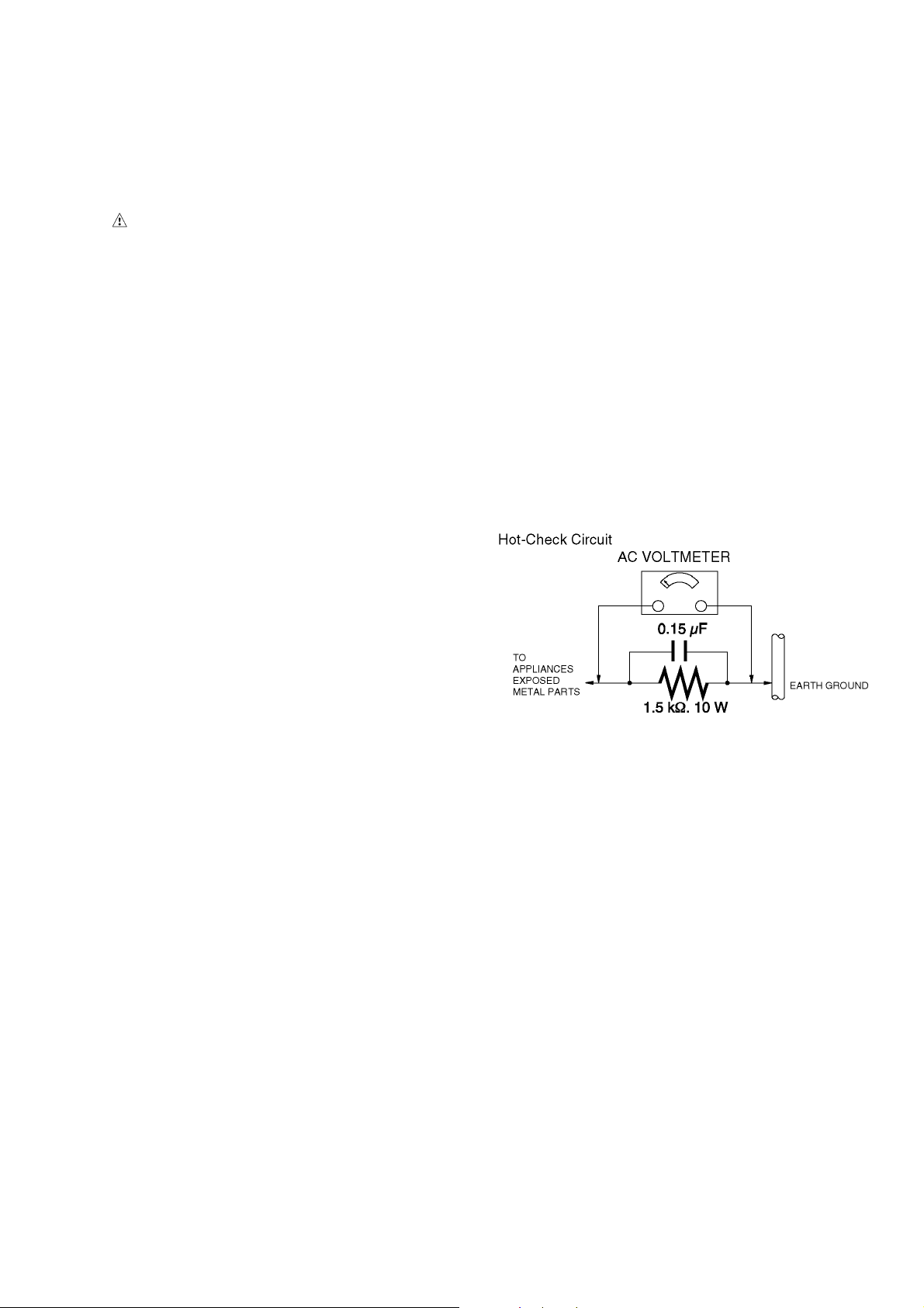
1.3. Leakage Current Hot Check
(See Figure 1.)
1. Plug the AC cord directly into the AC outlet. Do not use
an isolation transformer for this check.
2. Connect a 1.5 kΩ, 10 W resistor, in parallel with a 0.15 μF
capacitor, between each exposed metallic part on the set
and a good earth ground, as shown in Figure 1.
3. Use an AC voltmeter, with 1 kΩ/V or more sensitivity, to
measure the potential across the resistor.
4. Check each exposed metallic part, and measure the voltage at each point.
5. Reverse the AC plug in the AC outlet and repeat each of
the above measurements.
6. The potential at any point should not exceed 0.75 V RMS.
A leakage current tester (Simpson Model 229 or equivalent) may be used to make the hot checks, leakage current must not exceed 1/2 mA. In case a measurement is
outside of the limits specified, there is a possibility of a
shock hazard, and the equipment should be repaired and
rechecked before it is returned to the customer.
1.2. Leakage Current Cold Check
1. Unplug the AC cord and connect a jumper between the
two prongs on the plug.
2. Measure the resistance value, with an ohmmeter,
between the jumpered AC plug and each exposed metallic cabinet part on the equipment such as screwheads,
connectors, control shafts, etc. When the exposed metallic part has a return path to the chassis, the reading
should be between 1 MΩ and 5.2 MΩ. When the exposed
metal does not have a return path to the chassis, the
reading must be infinity.
Figure. 1
3
Page 4

2Warning
2.1. Prevention of Electrostatic Discharge (ESD) to Electrostatically
Sensitive (ES) Devices
Some semiconductor (solid state) devices can be damaged easily by static electricity. Such components commonly are called Electrostatically Sensitive (ES) Devices.
The following techniques should be used to help reduce the incidence of component damage caused by electrostatic discharge
(ESD).
1. Immediately before handling any semiconductor component or semiconductor-equipped assembly, drain off any ESD on your
body by touching a known earth ground. Alternatively, obtain and wear a commercially available discharging ESD wrist strap,
which should be removed for potential shock reasons prior to applying power to the unit under test.
2. After removing an electrical assembly equipped with ES devices, place the assembly on a conductive surface su ch as a luminum foil, to prevent electrostatic charge buildup or exposure of the assembly.
3. Use only a grounded-tip soldering iron to solder or unsolder ES devices.
4. Use only an antistatic solder removal device. Some solder removal devices not classified as "antistatic (ESD protected)" can
generate electrical charge sufficient to damage ES devices.
5. Do not use freon-propelled chemicals. These can generate electrical charges sufficient to damage ES devices.
6. Do not remove a replacement ES device from its protective package until immediately before you are ready to install it. (Most
replacement ES devices are packaged with leads electrically shorted together by conductive foam, aluminum foil or comparable conductive material).
7. Immediately before removing the protective material from the leads of a replacement ES device, touch the protective material
to the chassis or circuit assembly into which the device will be installed.
CAUTION :
Be sure no power is applied to the chassis or circuit, and observe all other safety precautions.
8. Minimize bodily motions when handling unpackaged replacement ES devices. (Otherwise harmless motion such as the
brushing together of your clothes fabric or the lifting of your foot from a carpeted floor can generate static electricity (ESD) sufficient to damage an ES device).
4
Page 5
2.2. Caution for AC Cord
(For the United Kingdom and
Republic of Ireland)
2.2.1. Information for Your Safety
IMPORTANT
Your attention is drawn to the fact that recording of prerecorded tapes or discs or other published or broadcast
material may infringe copyright laws.
WARNING
To reduce the risk of fire or shock hazard, do not expose
this equipment to rain or moisture.
CAUTION
To reduce the risk of fire or shock hazard and annoying
interference, use the recommended accessories only.
FOR YOUR SAFETY
DO NOT REMOVE THE OUTER COVER
To prevent electric shock, do not remove the cover. No user
serviceable parts inside. Refer servicing to qualified service
personnel.
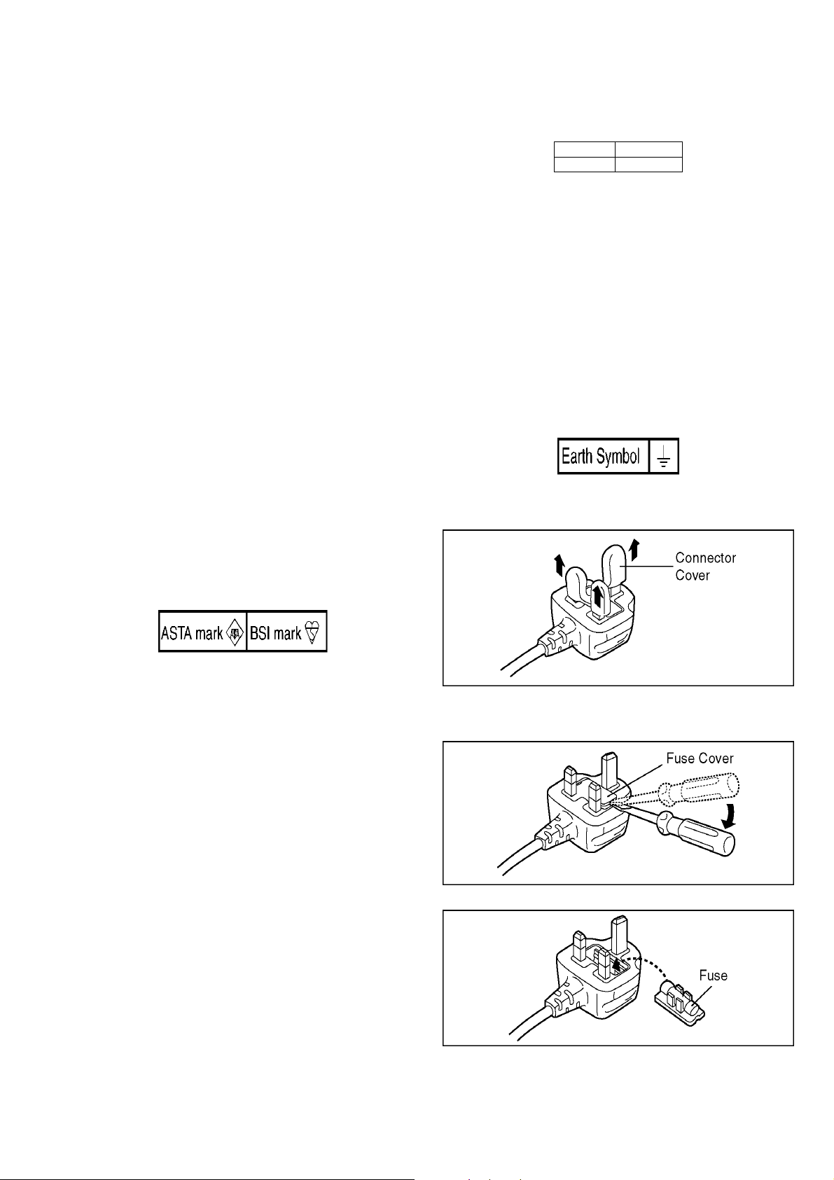
2.2.2. Caution for AC Mains Lead
For your safety, please read the following text carefully.
This appliance is supplied with a moulded three-pin mains plug
for your safety and convenience.
A 5-ampere fuse is fitted in this plug.
Should the fuse need to be replaced please ensure that the
replacement fuse has a rating of 5 amperes and it is approved
by ASTA or BSI to BS1362
Check for the ASTA mark or the BSI mark on the body of the
fuse.
2.2.2.1. Important
The wires in this mains lead are coloured in accordance with
the following code:
Blue Neutral
Brown Live
As the colours of the wires in the mains lead of this applianc e
may not correspond with the coloured markings identifying the
terminals in your plug, proceed as follows:
The wire which is coloured BLUE must be connected to the terminal in the plug which is marked with the letter N or coloured
BLACK.
The wire which is coloured BROWN must be connected to the
terminal in the plug which is marked with the letter L or coloured
RED.
Under no circumstances should either of these wi res be connected to the earth terminal of the three pin plug, marked with
the letter E or the Earth Symbol.
2.2.2.2. Before Use
Remove the Connector Cover as follows.
If the plug contains a removable fuse cover you must ensure
that it is refitted when the fuse is replaced.
If you lose the fuse cover, the plug must not be used until a
replacement cover is obtained.
A replacement fuse cover can be purchased from your local
Panasonic Dealer.
If the fitted moulded plug is unsuitable for the socket outlet in
your home then the fuse should be removed and the plug cut
off and disposed of safety.
There is a danger of severe electrical shock if the cut off plug is
inserted into any 13-ampere socket.
If a new plug is to be fitted please observe the wiring code as
shown below.
If in any doubt, please consult a qualified electrician.
2.2.2.3. How to Replace the Fuse
1. Remove the Fuse Cover with a screwdriver.
2. Replace the fuse and attach the Fuse cover.
5
Page 6
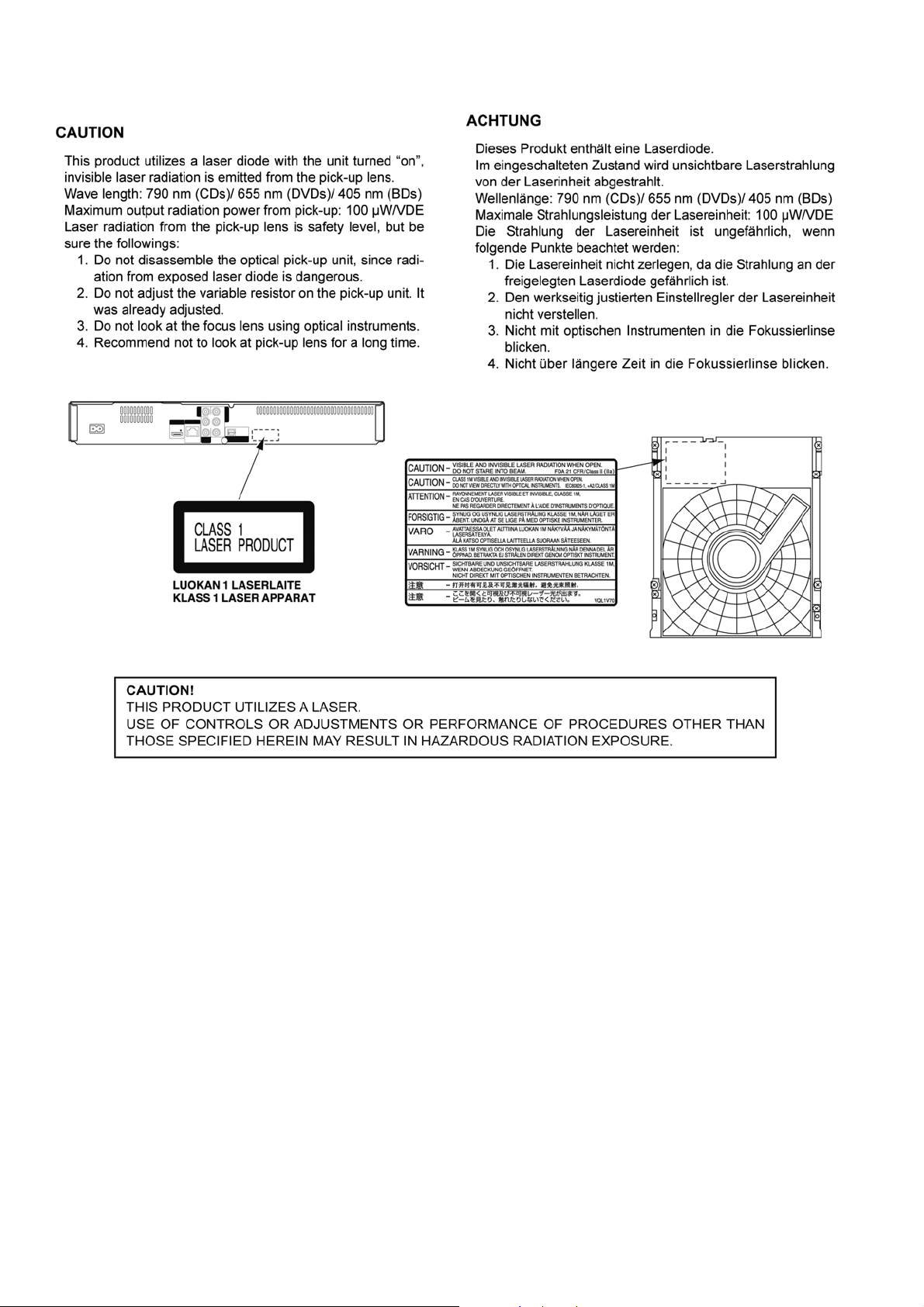
2.3. Precaution of Laser Diode
6
Page 7

2.4. Service Caution Based On Legal Restrictions
This service manual contains technical information, which allow service personnel’s to understand and service this model.
Please place orders using the parts list and not the drawing reference numbers.
If the circuit is changed or modified, the information will be followed by service manual to be controlled with original service manual.
2.4.1. General Description About Lead Free Solder (PbF)
The lead free solder has been used in the mounting proce ss of a ll electrical components on the printed circuit board s used for this
equipment in considering the globally environmental conservation.
The normal solder is the alloy of tin (Sn) and lead (Pb). On the other hand, the lead free solder is the alloy mainly consists of tin
(Sn), silver (Ag) and Copper (Cu), and the melting point of the lead free solder is higher approx.30°C (86°F) more than that of the
normal solder.
Distinction of P.C.B. Lead Free Solder being used
Service caution for repair work using Lead Free Solder (PbF)
• The lead free solder has to be used when repairing the equipment for which the lead free solder is used.
(Definition: The letter of “PbF” is printed on the P.C.B. using the lead free solder.)
• To put lead free solder, it should be well molten and mixed with the original lead free solder.
• Remove the remaining lead free solder on the P.C.B. cleanly for soldering of the new IC.
• Since the melting point of the lead free solder is higher than that of the normal lead solder, it takes the longer time to melt the
lead free solder.
• Use the soldering iron (more than 70W) equipped with the temperature control after setting the temperature at 350±30°C
(662±86°F).
Recommended Lead Free Solder (Service Parts Route.)
• The following 3 types of lead free solder are available through the service parts route.
RFKZ03D01KS-----------(0.3mm 100g Reel)
RFKZ06D01KS-----------(0.6mm 100g Reel)
RFKZ10D01KS-----------(1.0mm 100g Reel)
Note
* Ingredient: tin (Sn) 96.5%, silver (Ag) 3.0%, Copper (Cu) 0.5%, Cobalt (Co) / Germanium (Ge) 0.1 to 0.3%
7
Page 8
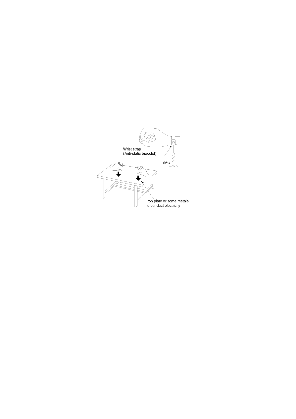
2.5. Static Electricity Protection Measures
• The laser diode in the traverse unit (optical pick-up) may break down due to potential difference caused by static electricity of
clothes or human body.
So, be careful of electrostatic breakdown during repair of the traverse unit (optical pick-up).
2.6. Ground for electrostatic breakdown prevention
• As for parts that use optical pick-up (laser diode), the optical pick-up is destroyed by the static electricity of the working environment.
Repair in the working environment that is grounded.
2.6.1. Work table grounding
• Put a conductive material (sheet) or steel sheet on the area where the traverse unit (optical pick- up) is placed, and ground t he
sheet.
2.6.2. Human body grounding
• Use the anti-static wrist strap to discharge the static electricity from your body.
2.6.3. When exchange the BDP Drive
• Before remove the ESD prevention bag, make sure to use the anti-static wrist strap to discharge the static electricity when
replace the BDP Drive.
Note:
The ESD prevention bag is used to replace the original short-circuit point.
It can be removed while placing the BDP Drive.
8
Page 9

3 Service Navigation
3.1. Service Infomation
This service manual contains technical information which will allow service personnel’s to understand and service this model.
Please place orders using the parts list and not the drawing reference numbers.
If the circuit is changed or modified, this information wil l be fol lowed by supp lement service ma nual to be filed with original servic e
manual.
1. This service manual does not contain the following information, because of the impossibility of servicing at component level.
• Schematic Diagram, Block Diagram and P.C.B. layout of Digital P.C.B., Drive P.C.B..
• Parts List for individual parts of Digital P.C.B..
• Exploded View and Parts List for individual parts of BD Drive.
2. The following category are recycle module part. Please send them to Central Repair Center.
• Digital P.C.B. (DMP-BDT100EE: RFKB76231DT)
• Digital P.C.B. (DMP-BDT100EG: RFKB76231BT)
• BD Drive: VXY2094
9
Page 10
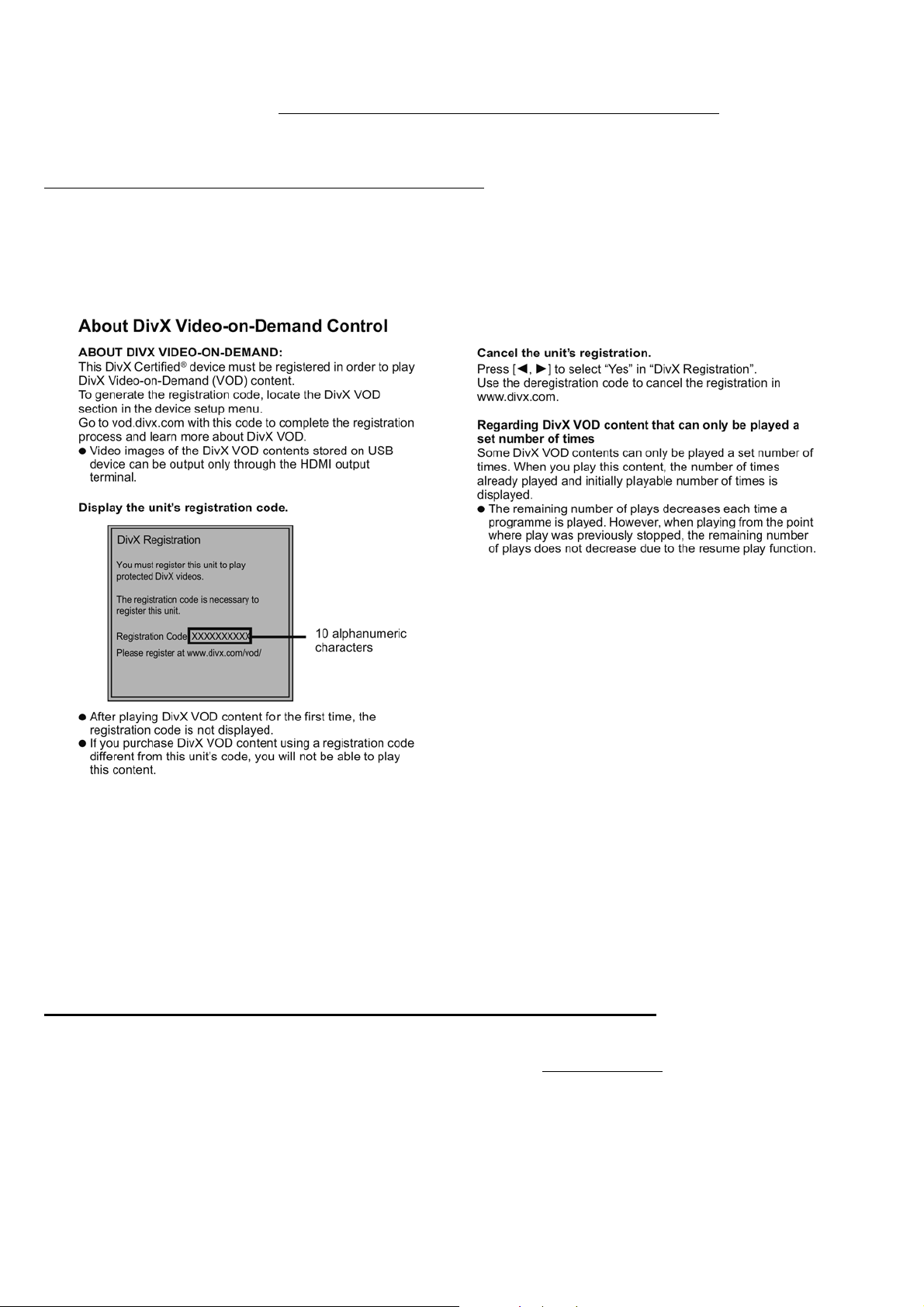
3.2. Caution for DivX
Please will always pass the customer “Warning for Customers Who Use the DivX Video-on-Demand content.” with the product and
get it when you unavoidably exchange FLASH ROM or P.C.B. including FLASH ROM (Wh en the product is exchanged, it is the
same.).
You must use print attached to service part (FLASH ROM or P. C.B. including FLASH ROM) or must use copy of print below as
“Warning for Customers Who Use the DivX Video-on-Demand content.”
Information needed without fail for the customer for whom it is used continuing DivX Video-on-Demand Service to “Manual for the
customer” is recorded.
Appendix:
*Parts that memorize user’s information are only FLASH ROM.
*The registration of Registration Code is possible for half a year up to 6 recorders up to 10 recorders a year.
Registration Code is memorized in FLASH ROM (Digital P.C.B.).
If exchange above P.C.B. or FLASH ROM, new registration Code differ from previous Registration Code will be generated.
In this case if your customer uses DivX Video-on-Demand service, he/she will no longer be able to play any content that he/she purchased under that same registration code.
Therefore your customer will need to obtain and register the new registration code.
*Copy this page and cut on the dotted line and give the lower half to your customer.
- - - - - - - - - - - - - - - - - - - - - - - - - - - - - - - - - - - - - - - - - - - - - - - - - - - - - - - - - - - - - - - - - - - - - - - - - - - - - - - - - - - - - - - - - - - - - - -
Warning for Customers Who Use the DivX Video-on-Demand content.
1. The registration code has been changed for the repair of the product or the product exchange.
2. Obtain and register a new registration code, otherwise you will no longer be able to play DivX Video-on-Demand content.
3. Follow the procedure on the DivX Video-on-Demand web site to register at http://vod.divx.com/
*If you do not use the DivX Video-on-Demand content, please ignore this warning.
10
.
Page 11

4 Specifications
Power supply: AC 220 to 240 V, 50 Hz
Power consumption: Approx. 24 W
In standby mode: Approx. 0.2 W
In quick start standby mode: Approx. 7 W
Operating temperature range: +5°C to +35°C
Operating humidity range: 10 % to 80 % RH (no condensation)
Signal system: PAL/NTSC
Video output:
Output level: 1.0 Vp-p (75 Ω)
Output connector: Pin jack (1 system)
Component video output:
(1080i/720p/480p/480i:60 Hz)
(1080i/720p/576p/576i:50 Hz)
Y output level: 1.0 Vp-p (75 Ω)
output level: 0.7 Vp-p (75 Ω)
P
B
P
output level: 0.7 Vp-p (75 Ω)
R
Output connector: Pin jack (Y:green, P
(1 system)
Video performance:
Horizontal resolution: More than 500 lines
Video S/N ratio: More than 65 dB
Audio output:
Output level: 2 Vrms (1 kHz, 0 dB)
Output connector: Pin jack
Number of connectors: 2 channel (1 system)
Audio performance:
Frequency response:
DVD(linear audio): 4 Hz to 22 kHz (48 kHz sampling)
4 Hz to 44 kHz (96 kHz sampling)
CD-Audio: 4 Hz to 20 kHz
S/N ratio: 100 dB
Dynamic range: 100 dB
Total harmonic distortion: 0.003 %
Digital audio output:
Optical digital output: Optical terminal
HDMI AV output:
Output format: 480p(525p)/1080i(1125i)/
720p(750p)/1080p(1125p)
HDMI (V.1.4a with 3D, Content
Type)
This unit supports “HDAVI Control 5”
function.
Output connector: TypeA (19 pin): 1 system
SD card slot:
Connector: 1 system
USB slot:
USB2.0: 1 system
Ethernet:
10BASE-T/100BASE-TX: 1 system
Optical pick-up: System with 2 lenses
Wave length: 790 nm (CDs)/655 nm (DVDs)/
405 nm (BDs)
LASER Specification
Class 1 LASER Product:
Wave length: 790 nm (CDs)/655 nm (DVDs)/
405 nm (BDs)
Laser power: No hazardous radiat ion is emitted
with the safety protection
Region management
information:
For the United Kingdom, Continental Europe and Republic of
Ireland (“EG” Model)
DVD-Video: region number “2” or “ALL”
BD-Video: region code “B”
For CIS and India (“EE” Model)
:blue, PR:red)
B
DVD-Video: region number “5” or “ALL”
BD-Video: region code “C”
Media:
Playable disc:
BD-Video (Blu-ray 3D, BDLIVE, BONUS VIEW): BD-ROM Version 2.4
BD-RE: Version3(Single Layer / Dual Layer),
JPEG
BD-R: V ersion2(Single Layer / Dual Layer),
4*5
DivX*
DVD-RAM: DVD Video Recording format,
AVCHD format, JPEG
DVD-R/DVD-R DL:
DVD-Video format*
1
,
DVD Video Recording format*
1
, JPEG*2, MP3*2,
1
,
DVD-RW:
AVCHD format*
2*3*5
DivX*
DVD-Video format*
DVD Video Recording format*
1
, AVCHD format*
1
+R/+RW/+R DL:
AVCHD format*
1
Video*
DVD-Video: DVD-Video format
CD-Audio: CD-DA
CD-R/CD-RW:
CD-DA, JPEG*
2
, MP3*2, DivX*2*
*1 Finalizing is necessary.
*2 ISO9660 level 1 or 2 (except for extended formats), Joliet
This unit is compatible with multi-session.
This unit is not compatible with packet writing.
*3 UDF1.02 without ISO9660, UDF1.5 with ISO9660
*4 UDF2.5
*5 DivX Certified to play DivX video up to Plus HD 1080p,
including premium content.
GMC (Global Motion Compensation) is not supported.
Maximum number of folders recognizable: 300 folders.
(including the root folder)
Maximum number of files recognizable: 200 files.
MPEG-4 AVC (H.264) profile is up to High Profile, Level 4.
AAC-LC, MP3 and Dolby Digital audio can be decoded.
SD card:
SD Memory Card*
6
JPEG, AVCHD format, MPEG-2
formatted FAT12, FAT16,
FAT32, exFAT*
7
*6 support SDHC, SDXC card
TM
support miniSD
support microSD
(need a microSD
Cards (need a miniSDTM Adaptor.)
TM
/microSDHC/microSDXC Cards
TM
Adaptor.)
*7 SDXC only
USB device:
USB Standard: USB 2.0 High Speed
MP3, JPEG, DivX
Format: FAT12, FAT16, FAT32
Contents:
JPEG:
(SD card, CD-R/CD-RW, DVD-RAM, DVD-R/DVD-R DL, BD-RE,
USB device)
File format: JPEG
Pixels: 34 x 34 to 8192 x 8192
Sub Sampling: 4:2:2, 4:2:0
Motion JPEG not supported.
SD card: JPEG conforming DCF (Design rule
for Camera File system)
Thawing Time: approx. 2sec (7M pixels)
Maximum folders: CD-R/CD-RW: 99
SD card, DVD-RAM, BD-RE,
DVD-R/DVD-R DL, US B d ev ic e : 300
1
,
1
,
5
11
Page 12

Maximum files: CD-R/CD-RW: 999
SD card, DVD-RAM, DVD-R/
DVD-R DL, USB device: 3000
BD-RE: 9999
MP3:
(CD-R/CD-RW, DVD-R/DVD-R DL, USB device)
File format: MP3
Compression rate: 32 kbps to 320 kbps
Sampling rate: 44.1 kHz, 48 kHz
AVCHD (H.264):
(DVD-RAM, DVD-R/DVD-R DL, DVD-RW, +R/+RW/+R DL,
SD Card)
File format: AVCHD format V1.0
Dimensions: 430mm(W) x 199mm(D) x 59mm(H)
Mass: Approx. 2.1 kg
Solder: This model uses lead free solder
Note: Specifications are subject to change
(excluding the projecting parts)
430mm(W) x 207mm(D) x 59mm(H)
(including the projecting parts)
(PbF).
without notice.
12
Page 13
4.1. Others (Licenses)
13
Page 14
5 Location of Controls and Components
2
10
11
12
1
2
13
3
14
15
16
4
5
17
18
6
1 Turn the unit on and off
2 TV operation buttons
You can operate the TV through the unit’s remote control.
[ TV] : Turn the television on and off
[AV] : Switch the input select
[KLVOL] : Adjust the volume
[9:CH] : Channel select
3 Select title numbers, etc./Enter numbers or characters
[CANCEL] : Cancel
4 Show playback menu
5 Switch on/off Secondary Video (Picture-in-picture)
6 Basic playback control buttons
7 Show status messages
8 Show Pop-up menu
9 Show Top menu/DIRECT NAVIGATOR
10 Show OPTION menu
11 Coloured buttons (red, green, yellow
These buttons are used when;
Operating a BD-Video disc that includes Java
applications (BD-J).
Displaying “Title View” and “Album View” screens.
Operating contents of VIERA CAST.
12 Transmit the remote control signal
13 Open or close the disc tray
, blue)
TM
CAUTION
7
19
8
20
9
21
22
Do not place objects in front of the unit. The disc tray may
collide with objects when it is opened, and this may cause
malfunction.
14 Adjust the volume of an amplifier/receiver.
15 Select audio
16 Reproduce more natural audio
17 Select drive (BD/DVD/CD, SD card or USB device)
18 Displays the Home screen of the VIERA CAST
19 Exit the menu screen
20 Show FUNCTION menu
21 Selection/OK, Frame-by-frame
22 Return to previous screen
5
1
1 Standby/on switch ( /I)
Press to switch the unit from on to standby mode or vice
versa. In standby mode, the unit is still consuming a
small amount of power.
Disc tray
3 Display
Disc indicator SD card indicator
The indicator blinks when reading data from a disc, a
card or a USB device, or writing data to a card.
2
6
USB device
indicator
3
7
4 Remote control signal sensor
Distance: Within approx. 7 m
Angle: Approx. 20G up and down, 30G left and right
5 Open or close the disc tray
6 SD card slot
7USBport
8Stop
9 Start play
4
Pull to flip down
the front panel.
9
8
14
Page 15
6 Operating Instructions
6.1. Taking out the Disc from BD Drive Unit when the Disc cannot be ejected
by OPEN/CLOSE button
6.1.1. When the power can be turned off.
6.1.1.1. When the power can be turned off.
1. Turn the unit off, then press and hold [OK], [Yellow] and [Blue] buttons on the remote control simultaneously for 5 seconds.
- “00 RET” is displayed on the unit’s FL display.
2. Repeatedly press the right cursor button on the remote Control or Power button on the u nit until “06 FTO” is displayed on the
unit's FL display.
3. Press [OK] button on the remote control or [OPEN/CLOSE] button on the unit.
6.1.1.2. When the power can not be turned off.
Press [POWER] button on the unit for over 4 seconds to turn off the power forcibly, and step 1 to 3 above.
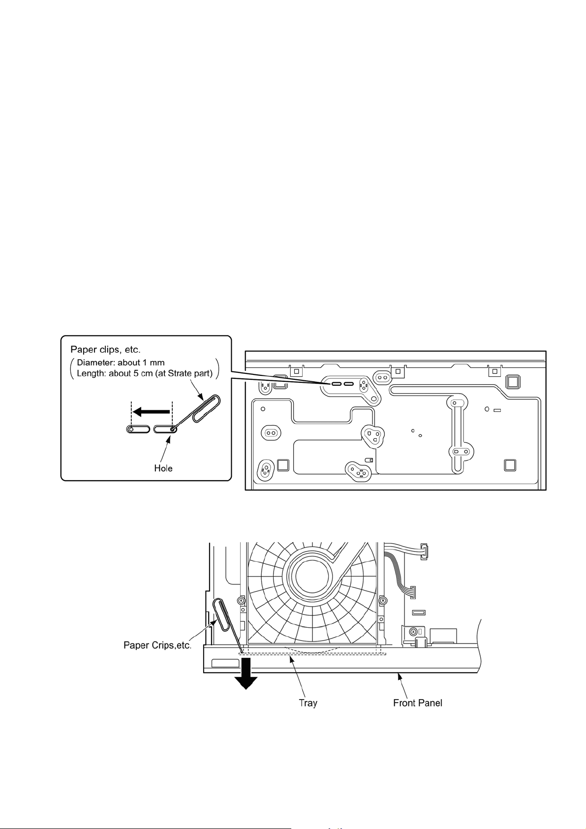
6.1.2. When the Forcible Disc Eject can not be done.
1. Turn off the power and pull out AC cord.
2. Remove the Top Case.
3. Put the unit so that bottom can be seen.
4. Insert paper clips, etc. into the hole on the bottom of BD Drive and slide th e paper clips, etc. in the direction of the arrow to
eject tray slightly.
5. Pull the unit upward, and push out Tray by paper clips, etc. or minus screw driver (small).
15
Page 16
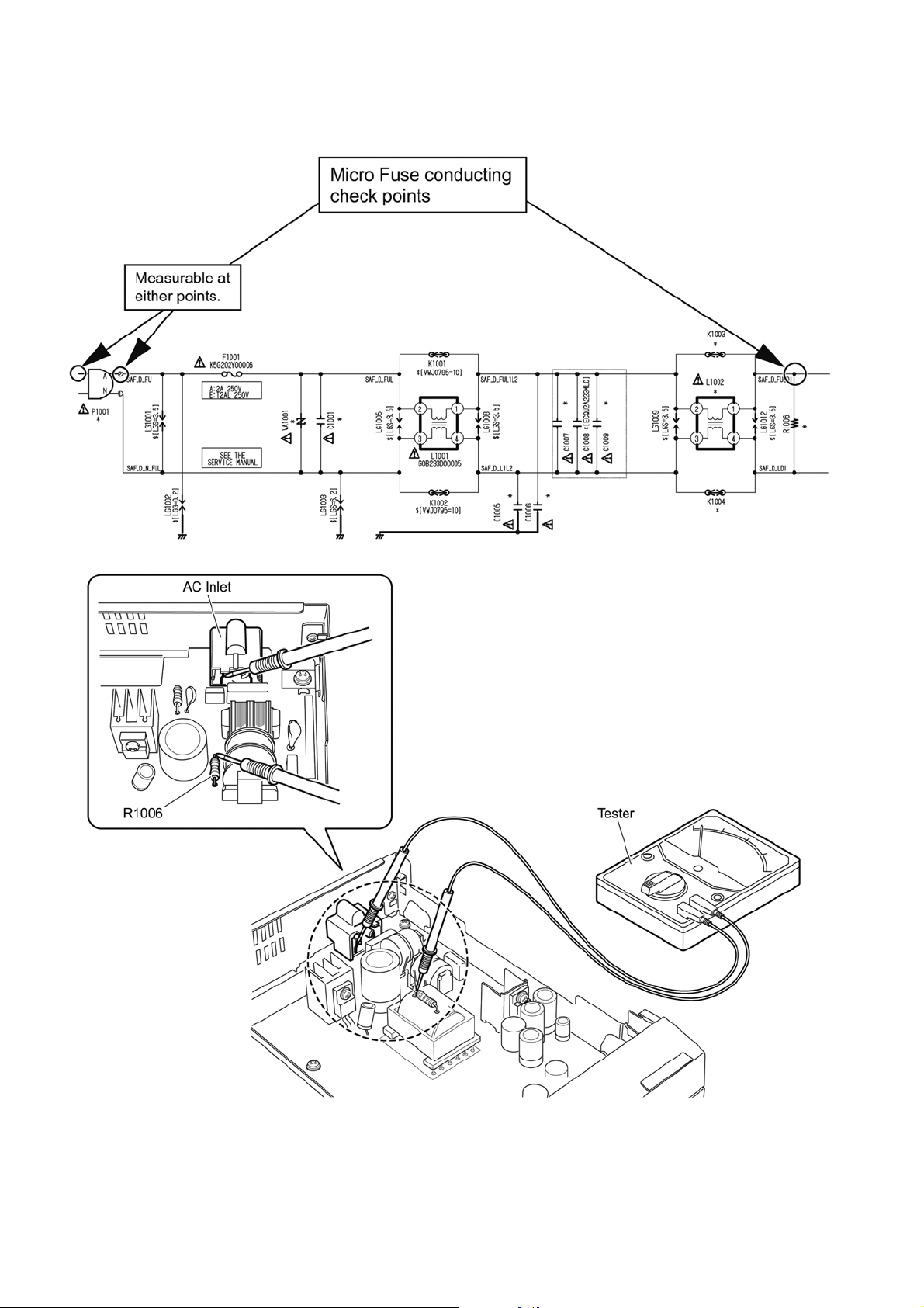
6.2. Micro Fuse Conducting Check
This unit uses the Micro Fuse.
Check the Micro Fuse conducting using the Tester at the check points below.
16
Page 17
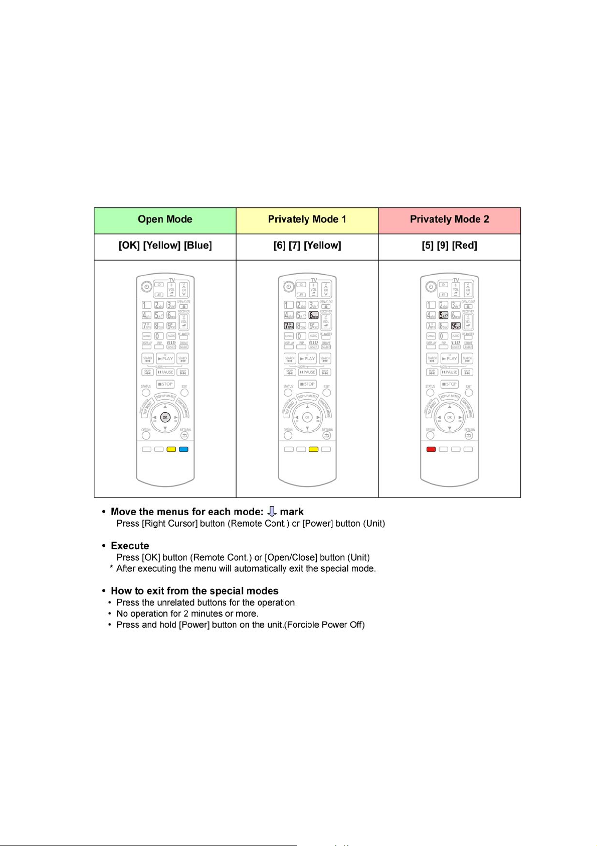
7 Multiple Pressing Function
7.1. About the Multiple Pressing of the Unit’s Remote Control
The remote control which included this unit is possible pressing multiple buttons simultaneously (Multiple Pre ssing function), and
can operate for the customer's initial settings and the Service Mode, etc.
The Multiple Pressing function is not available for conventional models' remote control. Use the remote control included this unit.
7.2. How to enter the Special Modes using the Multiple Pressing Function of
the Unit’s Remote Control
For pressing the multiple buttons of the remote control, this unit can be entering each of the following special modes.
After entering each mode, and then go to the menu you want to run.
17
Page 18
7.2.1. Open Mode (Remote Cont. Buttons: [OK] [Yellow] [Blue])
When pressing the 3 buttons, [OK], [Yellow] and [Blue] simultaneously for 5 seconds, “00 RET” is displayed on the FL display.
18
Page 19
7.2.2. Privately Mode 1 (Remote Cont. Buttons: [6] [7] [Yellow])
When pressing the 3 buttons, [6], [7] and [Yellow] simultaneously for 5 seconds, “50 RET” is displayed on FL display.
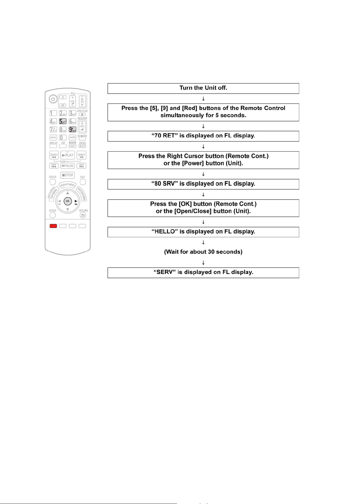
7.2.3. Privately Mode 2 (Remote Cont. Buttons: [5] [9] [Red])
When pressing the 3 buttons, [5], [9] and [Red] simultaneously for 5 seconds, “70 RET” is displayed on FL display.
19
Page 20
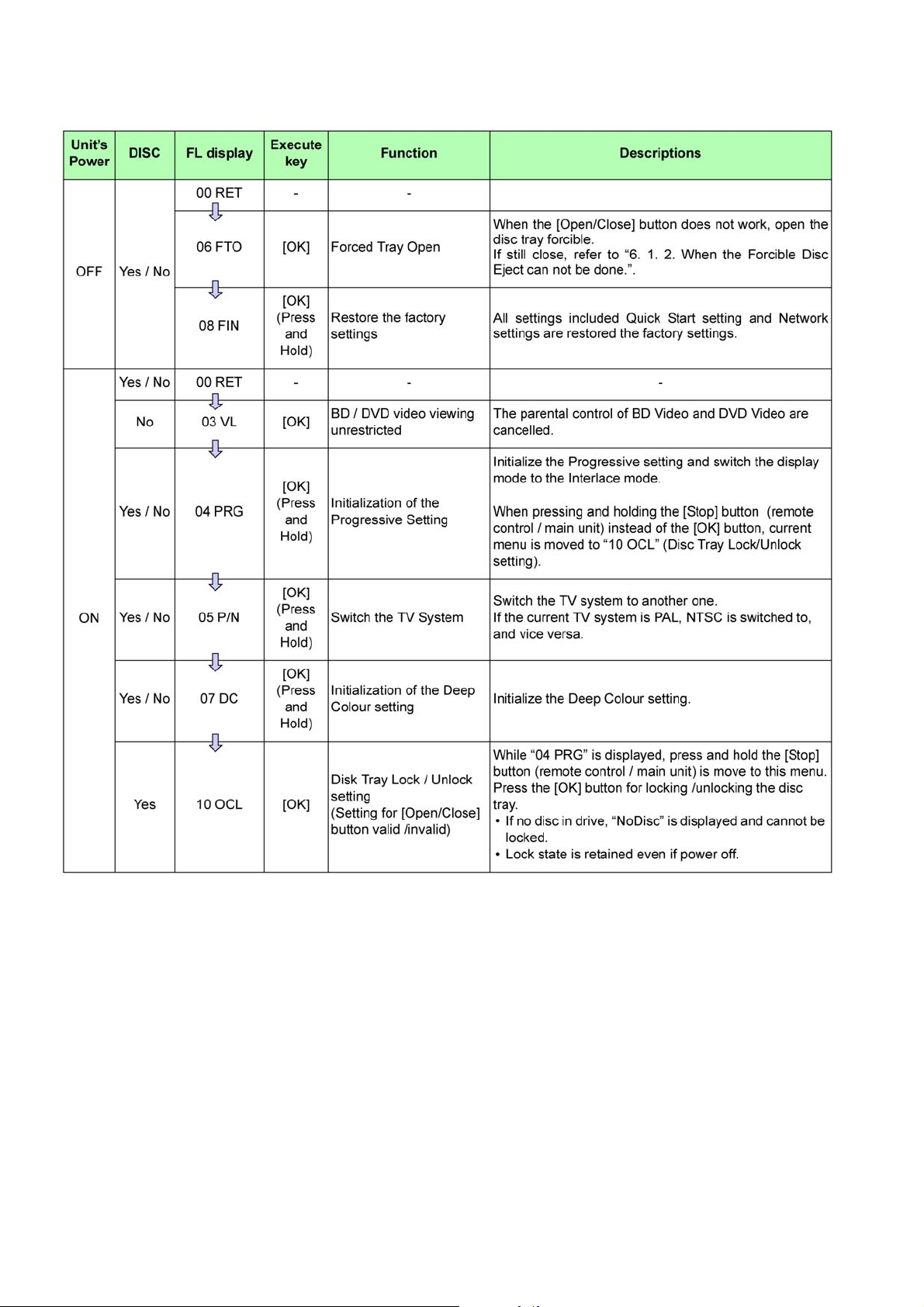
8 Service Mode
8.1. About the Service Mode
Informations necessary for service can be displayed.
8.1.1. How to enter the Service Mode
8.1.2. How to exit the Service Mode
Press and hold the [Power] button (remote control or unit).
>>> The Service Mode is terminated and automatically turns the unit off.
20
Page 21
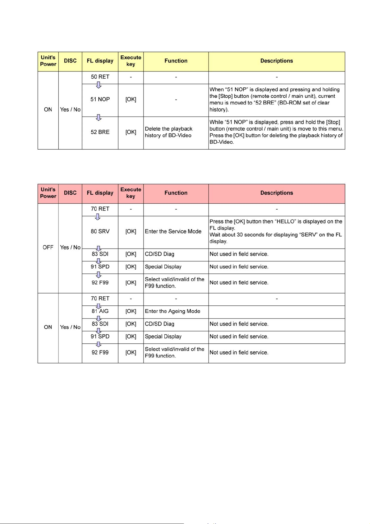
8.2. Service Mode List
The display of information to each command is as follows.
Note:
Do not use it excluding the designated command.
21
Page 22
222324
Page 23

Page 24

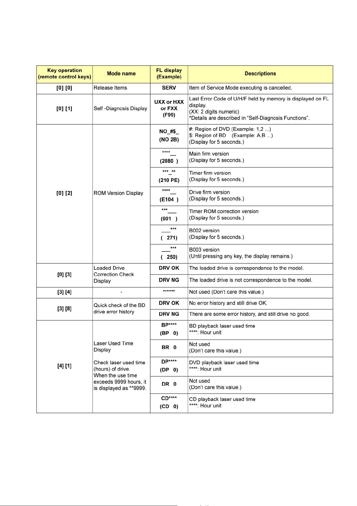
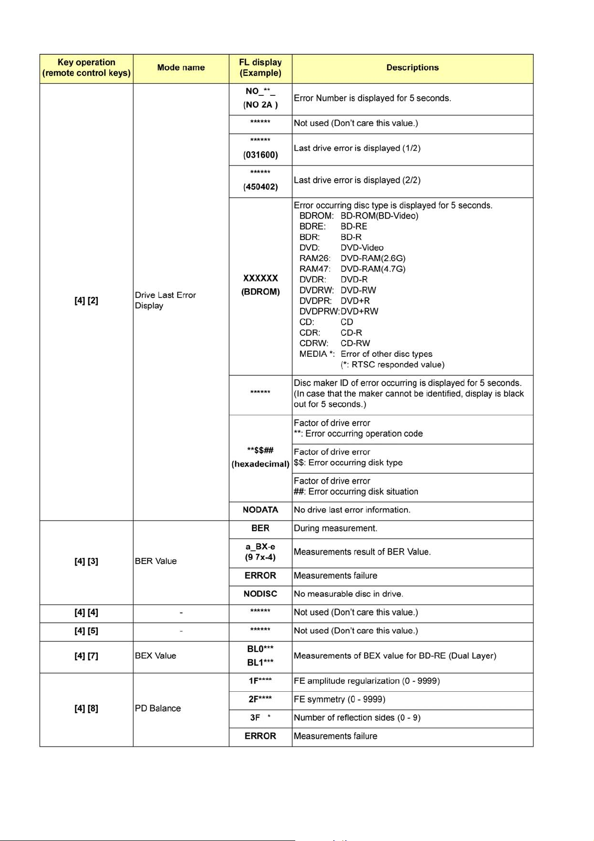
8.3. Self-Diagnostics Functions
8.3.1. Self-Diagnostics Functions
Self-Diagnosis Function provides information for errors to service personnel by Self-Diagnosis Display when any error has
occurred.
U** , H** and F** are stored in memory and held.
You can check last error code by transmitting [0] [1] of Remote Control in Service Mode.
Automatic Display on FL will be cancelled when the power is turned off or AC input is turned off during self-diagnosis display is ON.
Page 25

252627
Page 26

Page 27

9 Service Fixture & Tools
*The above parts are supplied by AVC-CSC-SPC.
Page 28

10 Disassembly and Assembly Instructions
10.1. Unit
10.1.1. Disassembly Flow Chart
The following chart is the procedure for disassembling the casing and inside parts for internal inspection when carrying out the servicing.
To assemble the unit, reverse the steps shown in the chart below.
10.1.2. P.C.B. Positions
28
Page 29

10.1.3. T op Case
1. Remove the 2 screws (A) and 3 screws (B).
2. Slide Top Case rearward and open th e both ends at rear
side of the Top Case a littl e and lift the Top Case in the
direction of the arrows.
10.1.5. Power SW P.C.B. and FL P.C.B.
10.1.5.1. Power SW P.C.B. and FL P.C.B.
1. Remove the screw (A).
2. Remove the Power SW P.C.B..
3. Remove the 3 screws (B).
4. Remove the FL P.C.B..
10.1.5.2. How to assemble the Tray door
ass’y
1. Attach the Tray door spring to Tray door ass’y.
10.1.4. Front Panel
1. Unlock 6 tabs (A) - (F) turn.
Pull with the Front Panel in the direction of your side.
2. Attach Tray door ass’y in order from [1] to [2].
[1]: Insert the shaft to the hole.
[2]: Insert the shaft to the hole.
29
Page 30

3. Confirm the Tray door spring is attached as following.
10.1.6. BD Drive Unit
1. Remove the wire with connector (A) and (B).
2. Remove the FFC.
3. Remove the 4 screws (A) to remove BD Drive Unit.
10.1.8. Rear Panel
1. Remove the 4 screws (A) and 1 screw (B).
2. Unlock 2 locking tabs (A) to remove the Rear Panel.
10.1.9. Power P.C.B.
1. Remove the wire with connector (A).
2. Remove the 2 screws (A) to remove Power P.C.B..
10.1.7. Chassis Angle
1. Remove the 2 screws (A) and remove the Chassis Angle.
10.1.10. Digital P.C.B.
1. Remove the wire with connector (A) , (B) and (C).
2. Remove the FFC.
3. Remove the 2 screws (A) to remove Digital P.C.B..
30
Page 31

10.2. BD Drive
10.2.1. Upper Base Ass’y
1. Remove the 4 Screws (A), and push the Hook in.
10.2.2. Tray
1. Perform the step “10. 2. 1. Upper Base Ass’y”.
2. Insert the paper clips, etc. into the hole of the bottom side,
and slide it to the direction of arrow until it can be.
3. Pull the Tray to the direction of arrow until it can be.
2. Lift up the Upper Base Ass’y, and pull it out to the direction of arrow.
4. Insert the paper clips, etc. into the hole of the Tray at 45
degrees, and lean it to the direction of arrow with pushing
the dotted point of the tray forward.
31
Page 32

5. Insert the paper clips, etc. into the Tray as below figure,
lift up the lever using the Eject Pin while pushing the dotted point of the Tray.
10.2.3. Pulley Gear, Belt
1. Perform the step “10. 2. 2. Tray”.
2. Push the Post to the direction of arrow by using the slotted screwdriver.
10.2.4. Slide Cam
1. Perform the step “10. 2. 3. Pulley Gear, Belt”.
2. Disconnect the 3 FFCs.
3. Remove the 2 Screws (B) to remove the Radiator Plate.
4. Open the connector lock, and disconnect the FFC (A).
5. Remove the Drive P.C.B..
3. Remove the Pulley Gear and Belt.
Caution:
Though the Drive P.C.B. is not supplied as replacement parts, it must be removed for after disassembling.
6. Open the connector lock, and disconnect the FFC.
7. Remove the 2 Screws (C), and remove the Traverse
Base Ass'y with spreading the 2 hooks to the direction of
arrows.
32
Page 33

8. Remove the Slide Cam.
10.2.5. Mid Gear, Drive Gear and Loading
Motor
1. Perform the step “10. 2. 4. Slide Cam”.
2. Remove the Mid Gear and Drive Gear.
3. Remove the Screw (D).
4. Remove the Screw (E), and remove the Switch P.C.B.
with the Loading Motor.
Remove the 2 soldering points, and remove the Loading
Motor.
33
Page 34

10.2.6. Grease
34
Page 35

10.2.7. How to Clean the Lens of the Optical Pick-UP
After performing the step “10. 2. 1. Upper Base Ass'y”, clean the lens of the Optical Pick-UP.
35
Page 36

10.2.8. How to Clean up the Turntable
When “NoREAD” is displayed in FL display, clean up the Turntable according to the following steps.
1. Blow the dust from the Turntable in the blower.
(Do not strongly blow it.)
2. Put one drop of isopropyl or ethyl alcohol to clean cotton swab.
(Using a fresh cotton swab does not use chemicals or additives.)
3. Using the cotton swab, wipe out the dust on the Turntable.
(Be careful not touching the surface of Turntable directly.)
36
Page 37

11 Measurements and Adjustments
For description of the disassembling procedure, see the “10 Disassembly and Assembly Instructions”.
11.1. Service Positions
1 1 .1.1. Checking and repairing of Power P.C.B.
37
Page 38

11.1.2. Checking and Repairing of BD Drive Unit/Digital P.C.B.
38
Page 39

11.2. Adjustment of BD Drive Unit/Digital P.C.B.
1 1.2.1. Checking out symptoms and repair of BD Drive Unit/Digital P.C.B.
39
Page 40

11.3. Caution for Replacing Parts
After replacing the Digital P.C.B., [TEST] is displayed, so, once power off again to on.
1 1.3.1. Caution after replacing parts
After replacing the BD Drive Unit/Digital P.C.B., must be update Firmware.
1 1.3.2. Standard Inspect Specifications after Repairs
After making repairs, we recommend performing the following inspection, to check normal operation.
40
Page 41

Table of contents
Service Manual
DSD1008038CE
Diagrams and Replacement
Parts List
Vol. 1
(K)...........Black Type
Colour
Model No.
DMP-BDT100EE
DMP-BDT100EG
Blu-ray Disc Player
Name of Signal
OFTR
FEP
This signal is connected
to the FEP schematic diagram.
Circuit name being connected.
6.Use the parts number indicated on the Replacement Parts List .
7.Indication on Schematic diagrams:
5.The voltage being indicated here may be include observational-error (deviation) due to
internal-resistance and/or reactance of equipment. Therefore, handle the value
indicated on here as reference.
4.Although the voltage and waveform available on here is measured with standard frame,
it may be differ from actual measurement due to modification of circuit and so on.
3.The voltage being indicated on the schematic diagram is measured in
"Standard-Playback" mode when there is no specify mode is mentioned.
2.It is only the "Test Round" and no terminal (Pin) is available on the P.C.B.
when the TP (Test Point) indicated as " " mark.
1.Although reference number of the parts is indicated on the P.C.B. drawing and/or
schematic diagrams, it is NOT mounted on the P.C.B. when it is displayed with "$" mark.
FOR SAFETY. WHEN REPLACING ANY OF THESE COMPONENTS USE ONLY THE SAME TYPE.
COMPONENTS IDENTIFIED WITH THE MARK HAVE THE SPECIAL CHARACTERISTICS
S1. About Indication of The Schematic Diagram
S1.1. Important Safety Notice
S1. About Indication of The Schematic Diagram ............................ S-1
S1.1. Important Safety Notice......................................................... S-1
S2. Voltage and Waveform Chart ................................................... S-2
S2.1. Power P.C.B. .........................................................................S-2
S3. Block Diagram .......................................................................... S-3
S3.1. Overall Block Diagram ..........................................................S-3
S3.2. Power Supply Block Diagram................................................ S-4
S3.3. Analog Video/Audio Block Diagram ...................................... S-5
S3.4. Timer Block Diagram ............................................................. S-6
S4. Schematic Diagram .................................................................. S-7
S4.1. Interconnection Diagram ....................................................... S-7
S4.2. FL Schematic Diagram .......................................................... S-8
S4.3. Power_SW Schematic Diagram ............................................ S-8
S4.4. Power Schematic Diagram.................................................. S-10
S6. Abbreviation ........................................................................... S-21
S7. Replacement Parts List .......................................................... S-25
S8. Exploded View .......................................................................S-31
S8.1. Frame and Casing Section.................................................. S-31
S8.2. Mechanism Section ............................................................. S-32
S8.3. Packing Parts and Accessories Section .............................. S-33
S5. Print Circuit Board .................................................................. S-14
S5.1. FL P.C.B. .............................................................................S-14
S5.2. Power_SW P.C.B. ............................................................... S-14
S5.3. Power P.C.B. .......................................................................S-16
S-1
Page 42

S2. Voltage and Waveform Chart
Note) Indicated voltage values are the standard values for the unit measured by the DC electronic circuit tester (high-impedance) with the chassis taken as standard.
Therefore, there may exist some errors in the voltage values, depending on the internal impedance of the DC circuit tester.
S2.1. Power P.C.B.
REF No.
IC1021 1 1.8 1.8
IC1021 2 1.6 1.5
IC1021 3 0.0 0.0
IC1021 4 16.5 16.5
IC1021 5 0.0 0.0
IC1021 6 - IC1021 7 321.0 319.0
IC1021 8 - IC1021 9 33.2 32.5
IC1102 1 0.0 0.0
IC1102 2 0.0 0.0
IC1102 3 8.3 8.4
IC1102 4 2.4 2.5
IC1130 1 4.4 4.5
IC1130 2 0.0 0.0
IC1130 3 0.0 0.0
IC1130 4 1.1 1.2
IC1130 5 1.2 1.3
IC1130 6 0.5 0.6
IC1130 7 5.3 5.5
IC1130 8 5.3 5.4
IC1130 9 1.1 1.2
IC1130 10 0.0 0.0
IC1130 11 0.0 0.0
IC1130 12 4.4 4.5
IC1130 13 5.7 5.9
IC1130 14 7.0 7.1
IC1130 15 9.9 10.6
IC1130 16 12.0 12.1
Q1022 1 9.4 9.5
Q1022 2 8.3 8.4
Q1022 3 0.0 0.0
Q1022 4 1.5 1.5
Q1023 1 1.1 1.2
Q1023 2 0.0 0.0
Q1023 3 0.0 0.0
Q1023 4 0.0 0.0
Q1131 1 5.8 5.8
Q1131 2 5.8 5.8
Q1131 3 10.0 10.6
Q1131 4 12.0 12.0
Q1131 5 5.8 5.8
Q1131 6 5.8 5.8
Q1170 1 11.3 11.3
Q1170 2 12.0 12.0
Q1170 3 11.9 11.9
Q1171 1 -0.2 -0.3
Q1171 2 0.0 0.0
Q1171 3 11.9 11.9
Q10101 1 0.1 0.0
Q10101 2 0.0 0.0
Q10101 3 5.8 5.8
QR1101 1 3.2 3.2
QR1101 2 0.0 0.0
QR1101 3 0.0 0.0
QR1131 1 3.2 3.2
QR1131 2 0.0 0.0
QR1131 3 0.0 0.0
QR1170 1 3.2 3.2
QR1170 2 0.0 0.0
QR1170 3 0.0 0.0
P1102 1 0.0 0.0
P1102 2 3.2 3.2
P1102 3 3.2 3.2
P1102 4 3.2 3.2
P1102 5 3.2 3.2
PIN No.
PB STOP
REF No.
PIN No.
P1102 6 2.1 2.2
P1102 7 3.2 3.2
P1102 8 3.2 3.2
P1102 9 3.2 3.2
P1102 10 3.2 3.2
P1102 11 - P1102 12 5.7 5.7
P1102 13 5.7 5.7
P1102 14 5.7 5.7
P1102 15 0.0 0.0
P1102 16 0.0 0.0
P1102 17 0.0 0.0
P1102 18 0.0 0.0
P1102 19 12.0 12.0
P1102 20 12.0 12.0
P1102 21 12.0 12.0
P1102 22 12.0 12.0
P1102 23 3.2 3.2
P1103 1 -18.5 -18.5
P1103 2 3.2 3.2
P1103 3 -15.6 -15.6
P1103 4 -21.0 -20.0
P1103 5 3.3 3.2
P1103 6 3.3 3.2
P1103 7 3.3 3.2
P1103 8 2.4 2.3
P1103 9 3.3 3.2
P1103 10 3.3 3.2
P1103 11 3.3 3.2
P1103 12 0.0 0.0
T1001 1 318.0 318.0
T1001 2 75.0 75.0
T1001 3 32.0 33.0
T1001 - - T1001 5 0.0 0.0
T1001 6 0.6 0.6
T1001 7 0.0 0.0
T1001 8 0.0 0.0
T1001 9 0.0 0.0
T1001 10 0.0 0.0
T1001 11 0.0 0.0
T1001 12 0.0 0.0
T1101 1 11.9 12.0
T1101 2 0.0 0.0
T1101 3 11.9 11.9
T1101 4 0.0 0.0
T1101 5 0.0 0.0
T1101 6 0.0 0.0
T1101 7 11.0 11.5
T1101 8 -18.5 -18.5
T1101 9 -18.5 -18.5
PB STOP
<IC1021>
<T1001>
S-2
Page 43

DMP-BDT100EE/EG OVERALL BLOCK DIAGRAM
TRAVERSE MECHANISM UNIT
OPTICAL
PICK-UP
UNIT
USB JACK
(FRONT)
X51006
IC57001
IC301
OPERATION/
TIMER
IC51001
AV DECODER/
SYSTEM CONTROLLER
L (MIX)
IC54002
R (MIX)
KEY
FL
V(COMPONENT)
PY
PB
CEC
PR
LASER DIODE
SERVO CONTROLLER/
OPTICAL DISC CONTROLLER
FOCUS COIL
TRACKING COIL
STEPPING
MOTOR
SPINDLE
MOTOR
LOADING
MOTOR
RESET
IC57005
AUDIO D/A
CONVERTER
IC55001
HDMI TX
DIGITAL
AUDIO OUT
(OPTICAL)
IC53001
VIDEO DRIVER
SD CARD
IC59020
IC51301
P59301
NAND FLASH
ROM/1GB
PHYSICAL LAYER
TRANSCEIVER
JK59001
ETHERNET
JACK
IC52201,IC52202
SDRAM/1GB
IC302
SERIAL FLASH
ROM/16Mbit
SDRAM/1GB
IC51004
PLL
IC52001,IC52002
REMOTE
SENSOR
HDMI
(JK55001)
JACK
AUDIO
X301
IC401
DISC
MOTOR
DRIVER
P51604
IC53002
IC101
LASER DIODE
DRIVER
S3. Block Diagram
S3.1. Overall Block Diagram
S-3
Page 44

DMP-BDT100EE/EG POWER SUPPLY CIRCUIT BLOCK DIAGRAM
F1001
P1001
(AC SOCKET)
A
N
VA1001,
L1001,1002
D1006,C1014
SURGE
SUPPRESSOR
AND
SURGE
ABSORBER
RECTIFIER
1
2
3
12
16
12
1
15
11
10
9
123
8
7
5
6
T1001
(POWER TRANSFORMER)
7
1
4
9
5
2
IC1021
(SWITCHING IC)
IC1130
(DC-DC CONVERTER)
IC1102
(SHUNT REGULATOR)
F/B
Z/C
3
GND
VCC
VIN
Q1022
(FEED BACK)
4
3
1
2
Q1131
(REGULATOR +5.9V)
4
3
1
5
6
2
Q1023
(FEED BACK)
4
3
1
2
Q10101
D1110
P1102
P58001
P1102
P58001
3
1
4
2
REF
CA
NC
QR1101
QR1131
D1027
D1026
D1029
D1031
D1032
VIN
V5
EN
EXT-Up
14
VB
13
LX
6
9
1
2
3
8
FB
OSC
7
RS+
8
RS-
P ch
MOS
FET
D
D
D
D
G
S
PW X SW12R2V
PW X SW5R9V
P1102
P58001
SP SAVE L
P1102
P58001
FL DCDC ON H
HOT COLD
T1101
(FL POWER
TRANSFORMER)
QR1170
Q1170
Q1171
9
5
12-14
23
19-22
10
To DIGITAL P.C.B.
P1103
3
P7001
P1103
1
P7001
F-
F+
VP
To FL P.C.B.
P1103
4
P7001
D1131 D1132
D1176
D1173
D1021
P1103
2
P7001
X SW3R3V
P1102
2
P58001
PW X SW3R3V
S3.2. Power Supply Block Diagram
S-4
Page 45

S3.3. Analog Video/Audio Block Diagram
IC57001
(TIMER)
IC53002
(OPTICAL FIBER
TRANSMITTER)
IC51001
(BP1 LSI)
DMP-BDT100EE/EG ANALOG VIDEO/AUDIO CIRCUIT BLOCK DIAGRAM
IC53001
(VIDEO DRIVER)
IC54002
(DAC)
1
SVDACO3
SYNC TIP
CLAMP
LPF
6.75MHz
LOGIC
MUTE
CTRL
LPF
13.5MHz
LPF
30MHz
3
SYNC TIP
CLAMP
VIN
PYIN
LPF
13.5MHz
8X
INTERPOLATOR
DE-EMPHASIS
CONTROL
CLOCK
DIVIDER MODULATOR
8X
INTERPOLATOR
LPF
30MHz
5
PBIN
LPF
13.5MHz
LPF
30MHz
7
8
6
7
8
2
PRIN
CTRL
15
14
13
12
11
10
4dB
2dB
2dB
2dB
2dB
4dB
4dB
4dB
VSAG
PYOUT
PYSAG
PBOUT
PROUT
VOUT
JK53001
(COMPONENT
AUDIO/VIDEO OUT)
VIDEO OUT
Y
PB
PR
AL
AR
SVDACO0
E 20
SVDACO1
B19
C15
Y OUT
(G Y OUT D)
PY OUT
(G PY OUT D)
PB OUT
(G PB OUT D)
SVDACO2
F19
PORT CA35
AF33
SBT2
G31
SBO2
H32
AO2DACCK
A22
AO2BCK
B22
AO2DMIX
B23
AO2LRCK
C20
AO2IEC
A21
PR OUT
(G PR OUT D)
CK53002
CK53001
CK53003
CK53004
CONTROL
INTERFACE
3
12
1
2
9
4
5
MODULATOR
AUDIO
DATA
INTERFACE
75
DRIVER
75
DRIVER
75
DRIVER
150k
BIAS
150k
BIAS
75
DRIVER
SCF
LPF
SCF
LPF
CSN
CCLK
CDTI
MCLK
BICK
SDTI
LRCK
AOUTL
AOUTR
SD L
4
CL57004
V OUT MUTE H
25
QR53001
VIN
VCC
DRIVER
IC
PW ADAC5V
1
10
PW ADAC5V
VDD
AVDD
2
16
PW ADAC5V
VCC1
VCC2
: VIDEO PB SIGNAL
: AUDIO PB SIGNAL
CK53006
CK53007
CK53008
S-5
Page 46

S3.4. Timer Block Diagram
IC57001
(TIMER)
DR PFAIL[L
]
SP SAVE L
SP SAVE L
G KEY3
G KEY1
G KEY2
G REMOCON
G FL TXD
G FL CLK
G FL CS
REMOCON
60
7
31
59
IC7001
(VFD DRIVER)
P110223P58001
P1103
8
P7001 P58001
6
P1102
P58001
12-14
P1102
P58001
19-22
P1102
PFAIL[L
]
VREF
VDD
6
IC57006
(REGULATOR)
4
1
5
VOUT
ON
VIN
PW X SW 5R9V
RESET
14
IC57005
(RESET)
12
OUTVDD
PW X SW12R2V
CL57014
CL57007
P1103
9
P7001 P58001
7
P1102
1
REMOCON
IR7001
REMOTE
SENSOR
27
FL TXD
18
FL CLK
20
FL CS[L
]
21
KEYIN2
2
P1103
10
P7001 P58001
8
P1102
KEYIN1 OP CL
1
P1103
11
P7001 P58001
9
P1102
KEYIN3 POWER
3
STOP
S7003
POWER
S7551
PLAY
S7002
OPEN/
CLOSE
S7001
REMOCON
KEY2
KEY1
PJ7004
1
PJ7551
KEY3
KEY POWER
POWER SW P.C.B.
FL P.C.B.
POWER P.C.B. DIGITAL P.C.B.
14
SG1
SG16
SG17
SG18
29
15
P15
P1
7
7G
6
P16
5
4
P17
P18
2
31
F-
1
F-
32
F+
F+
42
30
36
GR1
GR7
TIMER
DISPLAY
DP7001
P1103
3
P7001
P1103
1
P7001
P1103
6
P7001
P1103
5
P7001
P1103
7
P7001
P58001
4
P1102
P58001
3
P1102
P58001
5
P1102
F-
F+
VP
P1103
4
P7001
43
X SW3R3V
FL TXD
FL CLK
FL CS
PW X SW3R3V
P1103
2
P7001
P58001
2
P1102
VEE
VDD
13
VDD
6
DOUT
7
DIN
8
CLK
9
STB
FL DCDC
FL DCDC ON H
41
P110210P58001
2
DMP-BDT100EE/EG TIMER CIRCUIT BLOCK DIAGRAM
9
8
10MHz OUT
10MHz IN
X57001
(10MHz)
UARTP2M/TBUS TXD
UARTM2P/TBUS RXD
TBUS CLK
15
16
17
IC51001
(BP1 LSI)
AP24
AM24
AN24
SBPTM
AL23
XINTP
AM23
XINTM
AJ24
XMPREQ
SBMTP
SCLKM
CL57008 CL57010 CL57006 CL57011
CL57015 CL57013
TRY DILECT
40
CL57001
XINTM OUT
XINTP OUT
22
23
XINTM[TBUS
]
29
XMPREQ[TBUS
]
30
IC58006
(SWITCHING REGULATOR)
P STANDBY H
42
7
EN
IC58302
(REGULATOR)
DR P ON H
43
2
ON[H
]
TRY OP/CL
37
CL57003
CL57063
TRY PFAIL
50
Y31
XRST
SD BOOT
63
AK23
SDBOOT
XRES BP
51
To QR58001-B
IC58004
(DC-DC CONVERTER)
8
EN2
EN1
1
D58001
IC55002
(REGULATOR +5V)
HDMI P ON[H
]
55
1
5
4
ON
28
HDMI MONI(CEC IN)
26
HDMI CEC OUT
CL57028
CL57026
Q55001-55005
13
JK55001
(HDMI JACK)
CEC
18
+5V
VIN
VOUT
HD X SW5R9V
HDMI(CEC)
DRIVE
P53001 FP304
2 3
P53001 FP304
3 2
P53001 FP304
4 1
DRIVE P.C.B.
CL55001
CKS18
CKS13
13
1G
28
SG15
29
31
32
AJ23
XSRST
BP STATE
57
CL57057
S-6
Page 47

S4. Schematic Diagram
DMP-BDT100EE/EG INTERCONNECTION DIAGRAM
BD DRIVE UNITDRIVE P.C.B.
FP103
W 1
V 2
U 3
VH+ 4
U+ 5
U- 6
VH- 7
FP104
A- 1
B- 2
B+ 3
A+ 4
GND 5
XINRSW 6
FP102
CLOSE SW 1
GND 2
OPEN SW 3
LDM+ 4
LDM- 5
P1103
1 F2 X SW3R3V
3 F+
4 VP
5 FL CS
6 FL CLK
7 FL TXD
8 REMOCON
9 KEY2
10 KEY1
11 KEY3
12 GND
P1001
1 A
2 N
P1102
NC 1
PW X SW3R3V 2
FL CS 3
FL CLK 4
FL TXD 5
REMOCON 6
KEY2 7
KEY1 8
KEY3 9
FL DCDC ON H 10
NC 11
PW X SW5R9V 12
PW X SW5R9V 13
PW X SW5R9V 14
GND 15
GND 16
GND 17
GND 18
PW X SW12R2V 19
PW X SW12R2V 20
PW X SW12R2V 21
PW X SW12R2V 22
SP SAVE L 23
POWER SUPPLY P.C.B.
FL P.C.B.
POWER SW P.C.B.
P7001
1 F-
2 X SW3R3V
3 F+
4 VP
5 FL CS
6 FL CLK
7 FL TXD
8 REMOCON
9 KEY2
10 KEY1
11 KEY3
12 GND
PJ7004
KEY POWER 1
GND 2
PJ7551
KEY POWER 1
GND 2
P58001
1 NC
2 PW X SW3R3V
3 FL CS
4 FL CLK
5 FL TXD
6 REMOCON
7 KEY2
8 KEY1
9 KEY3
10 FL DCDC ON H
11 NC
12 PW X SW5R9V
13 PW X SW5R9V
14 PW X SW5R9V
15 GND
16 GND
17 GND
18 GND
19 PW X SW12R2V
20 PW X SW12R2V
21 PW X SW12R2V
22 PW X SW12R2V
23 SP SAVE L
DIGITAL P.C.B.
P53001
GND 1
BUSYLED 2
XEJECT 3
TRY PFAIL 4
P51602
GND 1
TX+ 2
TX- 3
GND 4
RX- 5
RX+ 6
GND 7
P58007
DR 5V 1
DRGND 2
DRGND 3
DR 12V 4
P301
1 GND SATA
2 DRX
3 NDRX
4 GND SATA
5 NDTX
6 DTX
7 GND SATA
P201
1 5V
2 MGND
3 GND
4 12V
FP304
4 GND
3 BUSYLED
2 XEJECT
1 TRY PFAIL
FP101
FCS2+ 1
FCS2- 2
TRK+ 3
FCS1+ 4
TRK- 5
FCS1- 6
A- 7
B- 8
A+ 9
B+ 10
GND PD 11
GND PD 12
GND PD 13
A(C/c/C) 14
B(B/b/B) 15
C(A/a/A) 16
D(D/d/D) 17
SA(F+J/e3+f3/E2) 18
SB(E+I/e2+f2/E1) 19
SC(H+L/e1+f1/F1) 20
SD(G+K/e4+f4/F2) 21
SW3 22
RF+ 23
RF- 24
SWB2 25
SWB1 26
VREF PD 27
VCC +5PD 28
GND PD 29
SW 30
GND 31
LDI BD 32
GND 33
LDI CD 34
GND 35
LDI DVD 36
GND 37
TEMP 38
VCC 39
VR DVD 40
VR CD 41
MD DVDCD 42
GND 43
MD BD 44
GND BDFPD 45
S4.1. Interconnection Diagram
S-7
Page 48

S4.2. FL Schematic Diagram / S4.3. Power_SW Schematic Diagram
Confidential
Until
2200
R7003
33
R7005
R7002
6200
R7009
82K
ZB7001 *
F1H1A105A028
C7002
10V
F1H1C104A071
C7006
16V
C7004
F1H1C104A071
16V
C7005
F1H1H104A783
50V
8 6 4 2 1579
32 31 28 2526
22 182021 19
24 232729
16 1314 11 10121517
A2BD00000200
DP7001
1
8
6
423
5
7
9
111210
P7001
K1KA12B00136
133
34
22
36 38 434140 42 44393735
20
6
18 1314
111210
17 1516
879
19
423
5
21
31
29
27
252324
26
28
30
32
C0HBB0000061
IC7001
EVQ11A05R
S7001
S7002
EVQ11A05R
S7003
EVQ11A05R
LB7003
$[J0JYC0000070]
321
G1 G2
IR7001
PNA4861M02VT
321
G1 G2
IR7002
$[B3RAD0000144]
1
2
PJ7004 REZ2025
PW-15V
PW-18V
PW-21V
PW_XN3R3V
STOPPLAY
KEY3
GND
GND
KEY2
KEY1
F-
F-
F-
or
or
or
or
or
(FL HOLDER)
KEY_POWER
P1
P2
5G
4G
P16
6G
7G
1GNC3G
2G
P18
P17
F+
F+
F+
P15
P13
P8
P7
P11
P12
P10
P9
P14
P4
P5P3P6
SG15 DOUT
LED4
[33]GR10
VEE
SG16 OSC
[23]SG10
[12]VSS
SG14 DIN
GR8
GR6
GR7
GR9
SG17
SG18
VDDVDD
VSS
GR3
GR5
GR4
GR1
GR2
LED3
LED2
[1]LED1
SG11
SG9
SG7
SG6
SG8
SG13
SG12 STB
CLK
SG1
K2
K1
SG4
SG5
SG2
SG3
REMOCON
FL_TXD
FL_CS
FL_CLK
VP
X_SW3R3V
2PIN FLAT CABLE 2.5mm PITCH
OPEN/CLOSE_SW
VariationCategory
ZB7001
DMP-BDT100P/GN DMP-BDT100EG
RMN0937-2 RMN0937-2J
Confidential
Until
S7551
EVQ11A05R
1
2
PJ7551
$[REZ2025]
POWER_SW
KEY_POWER
GND
DMP-BDT100EG/EE
Power_SW
Schematic Diagram
DMP-BDT100EG/EE
FL
Schematic Diagram
10987654321
G
F
E
D
C
B
A
S-8
Page 49

S-9
Page 50

C1031
*
*
C1006
*
C1005
C1009 *
C1007
*
C1001
*
*
C1019
C1008 $[ECQU2A223MLC]
*
R1006
*
R1011
*
R1012
R1013
*
VA1001
*
*
C1014
K1004
*
K1001
$[VWJ0795=10]
K1002
$[VWJ0795=10]
*
K1003
K1013
*
LG1008
$[LGS=3.5]
$[LGS=3.5]
LG1005
LG1003
$[LGS=6.2]
$[LGS=6.2]
LG1002
$[LGS=3.5]
LG1001
LG1012
$[LGS=3.5]
$[LGS=3.5]
LG1009
2 1
3 4
L1001
G0B233D00005
2 1
3 4
L1002
*
12
3 4
D1006
B0EDKT000009
K5G202Y00006
F1001
1
2
*
P1001
1
T1001
*
SAF_D_FULDI
SAF_D_DCV
SAF_D_DCV
SAF_D_DCV
SAF_D_LDISAF_D_L1L2
SAF_D_FUL1L2SAF_D_FUL
SAF_D_N_FUL
SAF_D_DCV_1
SAF_D_FU
(Y09140-1A)
XYN3+J8FJ
RADIATION
(S1WBA80-7062)
SEE THE
SERVICE MANUAL
A
N
VariationCategory1
C1001
C1005
C1006
C1007
C1009
C1014
C1018
C1019
C1021
C1023
C1024
C1026
C1031
D1012
D1021
D1029
D1110
IC1021
DMP-BDT100P DMP-BDT100EG/GN
C0DACZH00035 C0DACZH00017
B0JBSG000054 B0JBSL000002
B0BA01200046 B0BA01200046
$ B0HADV000001
$ B0HADV000001
$ F1B3D222A011
F1H1H222A013
│F1H1H222A219
F1H1H222A013
│F1H1H222A219
F1H1H101A004
│F1H1H1010005
F1H1H101A004
│F1H1H1010005
F1H1H471A792
│F1H1H471A004
F1H1H471A792
│F1H1H471A004
F1B3A122A009 F1B3D181A011
$ F1B2G681A015
F1B2G222A018 F1BAF1020020
F2B2E1010001 F2B2W4700003
$
F0CAF683A021
│ECQU2A683MLC
F0CAF223A021 $
F1BAF1020020 F1B2G471A014
F1BAF1020020 F1B2G471A014
F0CAF683A021
│ECQU2A683MLC
F0CAF683A021
│ECQU2A683MLC
VariationCategory
K1003
K1004
K1013
L1002
P1001
R1006
R1011
R1012
R1013
R1019
R1021
R1022
R1023
R1024
R1030
R1032
R1033
T1001
VA1001
ZA1021
ZA1023
DMP-BDT100P DMP-BDT100EG/GN
$ $
VSC5603-A VSC5603-A
ERZV05Z471CS
ERZV05Z471CS
│ERZV10D471C2
G4D2A0000313 G4D2A0000314
5600[G] 4700[G]
5100[G] 4700[G]
1500 3900
15K[G] 15K[G]
22K 10K
ERX2SZJR12E ERX2SJR33E
$(10K) $(10K)
$ $
$ ERG1SJ222E
$ ERG2SJ104P
$ ERG2SJ104P
$ D0BF685JA030
K2AB2B000007
│K2AB2B000011
K2AA2B000017
│K2AA2B000011
$ G0B233D00005
VWJ0795=5 $
VWJ0795=10 $
VWJ0795=10 $
HOT
COLD
CAUTION: FOR CONTINUED PROTECTION AGAINST FIRE HAZARD,
REPLACE ONLY WITH THE SAME TYPE 2A 250V FUSE.
ATTENTION: POUR UNE PROTECTION CONTINUE LES RISQUES
D' INCENDIE N' UTILISERQUE DES FUSIBLE DE MÉME TYPE 2A 250V.
2A 250V
2A 250V
DMP-BDT100EG/EE
Power
Schematic Diagram
1/4
N
M
L
K
J
I
H
G
S4.4. Power Schematic Diagram
S-10
S-10
Page 51

B0JAMD000026
D1176
D1174
$[B0AADM000003]
D1173
B0AADM000003
D1132 B0JCMD000014
D1131 B0JCMD000014
*
C1019
F1H1H221A004
50V220PC1135
50V
F1H1H120A004
C1134 50V12P
50V
C1175
F1H1H392A013
50V
$[F1K1C106A062]C1138
16V10
$[F1K1C106A062]C1139 16V10
F1K1C106A062
16V10uC1131
16V
C1133
50V0.015
F1H1H153A013
50V
16V0.1
C1132
F1H1C104A071
16V
F1H1C104A071
16V0.1C1137
16V
F1H1C104A071
16V0.1
C1136
16V
16V0.1
C1141
F1H1C104A071
16V
*
R1006
27K[D]
R1136
R1173
5600
ERDS2TJ470T
R1174
R1178
$(3300)
27K[D]
R1138
4700
R1172
R1171
4700
R1141
220K
470K[D]
R1139
470K[D]
R1137
R1177 $(47K)
R1175 $(47K)
470
R1176
R1145
D1BDR027A135
R1135
27K[D]
R1133
10K[D]220K[D]
R1134
R1132
2700
R1131
33K
82K
R1142
470K
R1143
5600
R1144
G1 G2
VSC6221
ZA1112
F2A1C221B111
C1174
16V
F2A1C8210008C1140 16V820[JG]
16V
C1176
F2A1C221B111
16V
C1173
F2A1H100B040
50V
C1172
F2A1V470A831
35V
$[F2A1H100B040]
C1171
D1171
B0BA02100019
B0BA03600021
D1172
B0BA01800019
D1175
D1110
*
B1BACG000058
Q1171
LG1012
$[LGS=3.5]
J0JHC0000048
LB1131
QR1170
B1GBCFJJ0040
B1GBCFNN0041
QR1131
13
4
15 1614
1236 578
12119 10
C0DBAYY00624
IC1130
L1105
G0A100ZA0045
5
2
6
13
4
Q1131
B1CHRD000024
2
9
1
6
7
8
4
3
5
T1101
G4D1A0000129
1
9
7
5
3
2
4
6
8
22
23
12
13
11
20
19
21
16
15
17
14
18
10
P1102
K1KY23AA0606
CKAA4
CKAA3
CKAA5
CKAA2
CKAA1
CKAB12
CKAB4
CKAB3
CKAB6
CKAB5
CKAB1
CKAB2
CKAB10
CKAB9
CKAB11
CKAB7
CKAB8
CKAA22
CKAA14
CKAA18
CKAA23
CKAA9
CKAA10
CKAA7
CKAA6
CKAA8
CKAA11
B1ADGF000010
Q1170
1
8
6
4
2
3
5
7
9
11
12
10
K1KB12B00040
P1103
1
T1001
*
SAF_D_FULDI
SAF_D_DCV
SAF_D_LDISAF_D_L1L2
PW_12R2V
PW_5R9VPW_A
PW_5R9VPW_C
PW_12R2VPW_B
or
or
or
or
or
or
or
or
or
or
or
or
or
or
or
or
or
or
or
or
(Y09140-1A)
XYN3+J8FJ
RADIATION
ZA1111
D1110
OSC
D
D
D
D
(CPH6350)
S
Vref/SS
GND
GND
GND
GND
GND
GND
GND
GND
G
AL1473
SEL/SYNC
EN VIN
EXT-Up
VB
RS+
RS-
CC
EXT-Lo
V5
LX
FB
FL_CLK
FL_CLK
PW_X_SW5R9V
PW_X_SW5R9V
PW_X_SW5R9V
PW_X_SW3R3V
FL_DCDC_ON_H
REMOCON
REMOCON
PW_X_SW12R2V
PW_X_SW12R2V
PW_X_SW12R2V
PW_X_SW12R2V
SP_SAVE_L
FL_TXD
FL_TXD
FL_CS
FL_CS
KEY1
KEY1
KEY3
KEY3
KEY2
KEY2
X_SW3R3V
V+
V-
NC
F+
F-
VP
VP
HOT
COLD
DMP-BDT100EG/EE
Power
Schematic Diagram
2/4
S-11
S-11
Page 52

D1021
*
D1012
*
B0ACCK000005
D1031
B0ACCK000005
D1026
D1032
B0ACCK000005
D1027
B0HAGM000006
*
C1021
C1024
*
C1023
*
C1026
*
C1031
*
*
C1006
*
C1005
C1009 *
C1007
C1018
*
*
C1019
$[F1A3D331A005]
C1022
C1008 $[ECQU2A223MLC]
$(0.1)
C1112
R1022
*
R1026
ERDS2TJ221T
$(4700)
R1105
4700
R1104
R1031
$
R1041
100K
R1042
100K
10[22]R1029
R1028 10[22]
*
R1011
*
R1012
R1013
*
R1021
*
R1023
*
R1024
*
R1030
*
R1032*R1033
*
R1019
G1 G2
*
ZA1023
G1 G2
*
ZA1021
51 3
2 4 7
9
IC1021
*
*
C1014
C1025
F2A1V6800002
35V68[JG]
35V
D1029
*
B0BA01600007
D1025
B0BC03200002
D1023
K1004
*
K1002
$[VWJ0795=10]
K1013
*
XYN3+J8FJZA1022
XYN3+J8FJZA1111
B1ABDF000033
Q10101
2 13
ZA1002
$[K9ZZ00001279]
2 13
ZA1001
K9ZZ00001279
$[LGS=3.5]
$[LGS=3.5]
LG1003
$[LGS=6.2]
$[LGS=6.2]
LG1002
$[LGS=3.5]
$[LGS=3.5]
$[LGS=3.5]
3 4
L1001
G0B233D00005
3 4
J0JKB0000003
LB1021
12
3 4
D1006
B0EDKT000009
4
3 2
1
B3PBA0000454
Q1022
4
3 2
1
B3PBA0000454
Q1023
1
10 11 12
56
7 98
23
T1001
*
SAF_D_VDS_1
SAF_D_VDS_1
SAF_D_DCV
SAF_D_DCV
SAF_D_DCV
SAF_D_LDISAF_D_L1L2
SAF_D_N_FUL
SAF_D_VDS
SAF_D_DCV_1
PW_12R2VPW_E
VEP71187A
VEP71186A
or
(Y09140-1A)
NP1
NP2
XYN3+J8FJ
RADIATION
IC1021 RADITION
(S1WBA80-7062)
ZA1022 XYN3+J8FJ
SEE THE
SERVICE MANUAL
(MR4020)
NS12-2
NS12-3
NS12-1
NC
DMP-BDT100EG/EE
Power
Schematic Diagram
I
H
G
F
E
D
C
B
A
3/4
S-12
Page 53

D1027
D1132 B0JCMD000014
D1131 B0JCMD000014
C1018
*
*
C1019
$(0.1)
C1112
F1H1C104A071
C1114
16V
C1124
F1H1C104A071
16V
F1H1H221A004
50V220PC1135
50V
$[F1K1C106A062]C1138
16V10
$[F1K1C106A062]C1139 16V10
F1K1C106A062
16V10uC1131
16V
C1133
50V0.015
F1H1H153A013
50V
16V0.1
C1132
F1H1C104A071
16V
F1H1C104A071
16V0.1C1137
16V
F1H1C104A071
16V0.1
C1136
16V
16V0.1
C1141
F1H1C104A071
16V
$(4700)
R1105
R1118
330[D]
R1116
2200
2200
R1112
4700
R1104
R1113
10K
R1111
1000
18K[D]
R1119
4700[D]
R1115
R1042
100K
27K[D]
R1136
27K[D]
R1138
R1141
220K
470K[D]
R1139
470K[D]
R1137
R1145
D1BDR027A135
R1135
27K[D]
R1133
10K[D]220K[D]
R1134
R1132
2700
R1131
33K
82K
R1142
470K
R1143
5600
R1144
G1 G2
VSC6221
ZA1112
C1125
F2A1C102A236
16V
F2A1C8210008C1140 16V820[JG]
16V
16V1000uF[JG]
F2A1C1020095
C1121
16V
16V1000uF[JG]
C1118
F2A1C1020095
16V
D1029
*
1 2 3
D1110
*
$[LGS=3.5]
J0JHC0000048
LB1131
4
3 2
1
B3PBA0000454
Q1022
4
3 2
1
B3PBA0000454
Q1023
4123
C0DBZMC00006
IC1102
QR1101
B1GBCFLL0042
B1GBCFNN0041
QR1131
13
4
15 1614
12119 10
G0A100ZA0045
L1103
G0A100ZA0045
4
1
9
7
5
3
2
4
6
8
12
13
11
10
P1102
K1KY23AA0606
CKAA4
CKAA3
CKAA5
CKAA2
CKAA1
CKAA9
CKAA10
CKAA7
CKAA6
CKAA8
CKAA11
Confidential
Until
1
10 11 12
56
7 98
23
T1001
*
SAF_D_DCV
SAF_D_LDISAF_D_L1L2
SAF_D_VDS
PW_12R2V
PW_12R2VPW_D
SP_SAVE_L
PW_12R2VPW_E
PW_5R9VPW_A
PW_5R9VPW_C
C
N.C REF
[MM1431CURE]
or
or
or
or
or
or
or
or
or
or
or
or
or
or
or
or
or
(Y09140-1A)
NP1
NP2
XYN3+J8FJ
RADIATION
ZA1111
D1110
OSC
(CPH6350)
S
Vref/SS
GND
GND
GND
G
SEL/SYNC
EN VIN
EXT-Up
VB
RS+
RS-
CC
EXT-Lo
V5
LX
FB
FL_CLK
PW_X_SW5R9V
PW_X_SW5R9V
PW_X_SW3R3V
FL_DCDC_ON_H
REMOCON
FL_TXD
FL_CS
KEY1
KEY3
KEY2
NC
2010/06/30
[PR]
NS12-2
NS12-3
NS12-1
NC
DMP-BDT100EG/EE
Power
Schematic Diagram
4/4
212019181716151413121110987654321
S-13
Page 54

IBT6
W753
W752
W751
R7009
R7005
R7003
LB7003
C7005
C7004
C7002
C7006
R7002
1
1
1
12
22
23
33
3
4
44
IC7001
MK2
MK1
W707
W702
W705
W703
W704
W706
W701
32
1
IR7002
1
43132 229
DP7001
S7001
S7002S7003
1
3
IR7001
12
PJ7004
1
2
12
11
P7001
DMP-BDT100EG/EE
Power_SW P.C.B.
DMP-BDT100EG/EE
FL P.C.B.
10987654321
G
F
E
D
C
B
A
(Foil Side)
(Component Side)
12
PJ7551
S7551
S5. Print Circuit Board
S5.1. FL P.C.B. / S5.2. Power_SW P.C.B.
S-14
Page 55

S-15
Page 56

W12
W15
W3
ZA1023
K1013
ZA1021
ZA1112
R1011
R1012
D1021
D1012
C1031
R1013
VA1001
6 5 2 13
T1001
D1025
R1026
R1022
LB1021
9
75432
1
IC1021
D1027
C1025
C1022
C1021
D1029
C1014
R1006
2
1
4 3
L1002
2
1
4 3
L1001
K1004
K1003
K1002
K1001
F1001
C1019
C1018
C1009C1008C1007
C1006
C1005
C1001
P1001
3
1
ZA1001
3
1
ZA1002
(Component Side)
1/4
N
M
L
K
J
I
H
G
DMP-BDT100EG/EE
Power P.C.B.
S5.3. Power P.C.B.
S-16
S-16
Page 57

3.53.5
3.53.5
6.26.2
3.5
R1019
4
3 2
1
Q1023
4
3 2
1
Q1022
C1112
C1124
1
R1104
R1105
R1111
R1112
R1113
R1116
QR1101
D1023
R1042
R1041
R1033
R1032
R1031
R1030
R1029
R1028
R1024
R1023
R1021
Q10101
D1032
D1031
D1026
C1026
C1024
C1023
LG1012
LG1009
LG1008
LG1005
LG1003
LG1002
LG1001
+
-
D1006
2/4
DMP-BDT100EG/EE
Power P.C.B.
(Foil Side)
S-17
S-17
Page 58

W14
W7
W10
W4
W9
W12
W15
W2
W5
W6
W1
W8
W11
W13
K1013
ZA1112
R1013
121110987
6 5 2 13
T1001
C1176
R1174
Q1171
D1172
9
8
7
6
5 4
3
2
1
T1101
D1176
D1174
D1173
D1171
C1171
C1174
D1175
C1173
C1172
C1125
L1105
C1118
D1110
C1121
L1103
C1140
D1025
R1026
LB1021
D1027
C1025
C1014
4 3
K1004
C1019
C1018
C1005
22
23
1
2
P1102
1
2
11
12
P1103
I
H
G
F
E
D
C
B
A
3/4
(Component Side)
(Component Side)
DMP-BDT100EG/EE
Power P.C.B.
S-18
Page 59

CKAB1
CKAA11
CKAA9
CKAA7
CKAA5
CKAA3
CKAA1
CKAA8
CKAA6
CKAA4
CKAA2
CKAB2
CKAB4
CKAB3
CKAB12
CKAB10
CKAB9
CKAB8
CKAB6
CKAB5
CKAB7
CKAB11
CKAA10
CKAA18
CKAA23
CKAA22
C1175
R1173
Q1170
R1171
QR1170
R1172
R1177
R1176
R1175
R1178
4
3 2
1
Q1023
4
3 2
1
Q1022
CKAA14
R1135
R1134
R1133
R1138
R1139
R1137
C1132
R1131
C1133
R1132
C1138
R1142
R1141
QR1131
R1143
C1135
C1136
C1139
R1115
R1119 R1118
1 8
916
IC1130
C1137
C1141
R1144
LB1131
D1132
D1131
C1131
4
61
3
Q1131
C1134
R1136
R1145
C1112
C1114
C1124
3 2
4
1
IC1102
R1104
R1105
R1111
R1112
R1113
R1116
QR1101
D1023
R1042
R1041
R1029
R1028
R1024
D1026
C1023
LG1012
LG1009
+
-
DMP-BDT100EG/EE
Power P.C.B.
(Foil Side)
4/4
212019181716151413121110987654321
(Foil Side)
S-19
Page 60

S-20
Page 61

S6. Abbreviation
INITIAL/LOGO
A A0~UP ADDRESS
ACLK AUDIO CLOCK
AD0~UP ADDRESS BUS
ADATA AUDIO PES PACKET DATA
ALE ADDRESS LATCH ENABLE
AMUTE AUDIO MUTE
AREQ AUDIO PES PACKET REQUEST
ARF AUDIO RF
ASI SERVO AMP INVERTED INPUT
ASO SERVO AMP OUTPUT
ASYNC AUDIO WORD DISTINCTION SYNC
B BCK BIT CLOCK (PCM)
BCKIN BIT CLOCK INPUT
BDO BLACK DROP OUT
BLKCK SUB CODE BLOCK CLOCK
BOTTOM CAP. FOR BOTTOM HOLD
BYP BYPATH
BYTCK BYTE CLOCK
C CAV CONSTANT ANGULAR VELOCITY
CBDO CAP. BLACK DROP OUT
CD COMPACT DISC
CDSCK CD SERIAL DATA CLOCK
CDSRDATA CD SERIAL DATA
CDRF CD RF (EFM) SIGNAL
CDV COMPACT DISC-VIDEO
CHNDATA CHANNEL DATA
CKSL SYSTEM CLOCK SELECT
CLV CONSTANT LINEAR VELOCITY
COFTR CAP. OFF TRACK
CPA CPU ADDRESS
CPCS CPU CHIP SELECT
CPDT CPU DATA
CPH1~3 CLOCK PULSE SOURCE DRIVE
CPUADR CPU ADDRESS LATCH
CPUADT CPU ADDRESS DATA BUS
CPUIRQ CPU INTERRUPT REQUEST
CPRD CPU READ ENABLE
CPV GATE DRIVER CLOCK PULSE
CPWR CPU WRITE ENABLE
CS CHIP SELECT
CSYNCIN COMPOSITE SYNC IN
CSYNCOUT COMPOSITE SYNC OUT
D DACCK D/A CONVERTER CLOCK
DEEMP DE-EMPHASIS BIT ON/OFF
DEMPH DE-EMPHASIS SWITCHING
DIG0~UP FL DIGIT OUTPUT
DIN DATA INPUT
DMSRCK DM SERIAL DATA READ CLOCK
DMUTE DIGITAL MUTE CONTROL
DO DROP OUT
DOUT0~UP DATA OUTPUT
DRF DATA SLICE RF (BIAS)
DRPOUT DROP OUT SIGNAL
ABBREVIATIONS
S-21
Page 62

INITIAL/LOGO
ABBREVIATIONS
DREQ DATA REQUEST
DRESP DATA RESPONSE
DSC DIGITAL SERVO CONTROLLER
DSLF DATA SLICE LOOP FILTER
DVD DIGITAL VIDEO DISC
E EC ERROR TORQUE CONTROL
ECR ERROR TORQUE CONTROL REFERENCE
ENCSEL ENCODER SELECT
ETMCLK EXTERNAL M CLOCK (81MHz/40.5MHz)
ETSCLK EXTERNAL S CLOCK (54MHz)
F FBAL FOCUS BALANCE
FCLK FRAME CLOCK
FE FOCUS ERROR
FFI FOCUS ERROR AMP INVERTED INPUT
FEO FOCUS ERROR AMP OUTPUT
FG FREQUENCY GENERATOR
FSC FREQUENCY SUB CARRIER
FSCK FS (384 OVER SAMPLING) CLOCK
G GND COMMON GROUNDING (EARTH)
H HA0~UP HOST ADDRESS
HD0~UP HOST DATA
HINT HOST INTERRUPT
HRXW HOST READ/WRITE
I IECOUT IEC958 FORMAT DATA OUTPUT
IPFRAG INTERPOLATION FLAG
IREF I (CURRENT) REFERENCE
ISEL INTERFACE MODE SELECT
L LDON LASER DIODE CONTROL
LPC LASER POWER CONTROL
LRCK L CH/R CH DISTINCTION CLOCK
M MA0~UP MEMORY ADDRESS
MCK MEMORY CLOCK
MCKI MEMORY CLOCK INPUT
MCLK MEMORY SERIAL COMMAND CLOCK
MDATA MEMORY SERIAL COMMAND DATA
MDQ0~UP MEMORY DATA INPUT/OUTPUT
MDQM MEMORY DATA I/O MASK
MLD MEMORY SERIAL COMMAND LOAD
MPEG MOVING PICTURE EXPERTS GROUP
O ODC OPTICAL DISC CONTROLLER
OEH SOURCE DRIVER OUTPUT ENABLE
OEV 1, 2 GATE DRIVER OUTPUT ENABLE
OFTR OFF TRACKING
OSCI OSCILLATOR INPUT
OSCO OSCILLATOR OUTPUT
OSD ON SCREEN DISPLAY
P P1~UP PORT
PCD CD TRACKING PHASE DIFFERENCE
PCK PLL CLOCK
PDVD DVD TRACKING PHASE DIFFERENCE
PEAK CAP. FOR PEAK HOLD
PLLCLK CHANNEL PLL CLOCK
PLLOK PLL LOCK
S-22
Page 63

INITIAL/LOGO
ABBREVIATIONS
PWMCTL PWM OUTPUT CONTROL
PWMDA PULSE WAVE MOTOR DRIVE A
PWMOA, B PULSE WAVE MOTOR OUT A, B
R RE READ ENABLE
RFENV RF ENVELOPE
RFO RF PHASE DIFFERENCE OUTPUT
RS (CD-ROM) REGISTER SELECT
RSEL RF POLARITY SELECT
RST RESET
RSV RESERVE
S SBI0, 1 SERIAL DATA INPUT
SBO0 SERIAL DATA OUTPUT
SBT0, 1 SERIAL CLOCK
SCK SERIAL DATA CLOCK
SCKR AUDIO SERIAL CLOCK RECEIVER
SCL SERIAL CLOCK
SCLK SERIAL CLOCK
SDA SERIAL DATA
SEG0~UP FL SEGMENT OUTPUT
SELCLK SELECT CLOCK
SEN SERIAL PORT ENABLE
SIN1, 2 SERIAL DATA IN
SOUT1, 2 SERIAL DATA OUT
SPDI SERIAL PORT DATA INPUT
SPDO SERIAL PORT DATA OUTPUT
SPEN SERIAL PORT R/W ENABLE
SPRCLK SERIAL PORT READ CLOCK
SPWCLK SERIAL PORT WRITE CLOCK
SQCK SUB CODE Q CLOCK
SQCX SUB CODE Q DATA READ CLOCK
SRDATA SERIAL DATA
SRMADR SRAM ADDRESS BUS
SRMDT0~7 SRAM DATA BUS 0~7
SS START/STOP
STAT STATUS
STCLK STREAM DATA CLOCK
STD0~UP STREAM DATA
STENABLE STREAM DATA INPUT ENABLE
STH SOURCE START PULSE
STSEL STREAM DATA POLARITY SELECT
STV GATE DRIVER SCAN START PULSE
STVALID STREAM DATA VALIDITY
SUBC SUB CODE SERIAL
SBCK SUB CODE CLOCK
SUBQ SUB CODE Q DATA
SYSCLK SYSTEM CLOCK
T TE TRACKING ERROR
TIBAL BALANCE CONTROL
TID BALANCE OUTPUT 1
TIN BALANCE INPUT
TIP BALANCE INPUT
TIS BALANCE OUTPUT 2
TPSN OP AMP INPUT
S-23
Page 64

INITIAL/LOGO
ABBREVIATIONS
TPSO OP AMP OUTPUT
TPSP OP AMP INVERTED INPUT
TRCRS TRACK CROSS SIGNAL
TRON TRACKING ON
TRSON TRAVERSE SERVO ON
V VBLANK V BLANKING
VCC COLLECTOR POWER SUPPLY VOLTAGE
VCDCONT VIDEO CD CONTROL (TRACKING BALANCE)
VDD DRAIN POWER SUPPLY VOLTAGE
VFB VIDEO FEED BACK
VREF VOLTAGE REFERENCE
VSS SOURCE POWER SUPPLY VOLTAGE
W WAIT BUS CYCLE WAIT
WDCK WORD CLOCK
WEH WRITE ENABLE HIGH
WSR WORD SELECT RECEIVER
X X X' TAL
XALE X ADDRESS LATCH ENABLE
XAREQ X AUDIO DATA REQUEST
XCDROM X CD ROM CHIP SELECT
XCS X CHIP SELECT
XCSYNC X COMPOSITE SYNC
XDS X DATA STROBE
XHSYNCO X HORIZONTAL SYNC OUTPUT
XHINT XH INTERRUPT REQUEST
XI X' TAL OSCILLATOR INPUT
XINT X INTERRUPT
XMW X MEMORY WRITE ENABLE
XO X' TAL OSCILLATOR OUTPUT
XRE X READ ENABLE
XSRMCE X SRAM CHIP ENABLE
XSRMOE X SRAM OUTPUT ENABLE
XSRMWE X SRAM WRITE ENABLE
XVCS X V-DEC CHIP SELECT
XVDS X V-DEC CONTROL BUS STROBE
XVSYNCO X VERTICAL SYNC OUTPUT
S-24
Page 65

S7. Replacement Parts List
Definition of Parts supplier:
1. Parts marked with [CHPAVC] in the remarks column are supplied from CHPAVC.
Others are supplied from PAVCSK.
S-25
Page 66

DMP-BDT100EG,EE vol.1
Ref.No. Part No. Part Name & Description Pcs Remarks Ref.No. Part No. Part Name & Description Pcs Remarks
C1175 F1H1H392A013 50V 3900P 1
## VEP70362B FL P.C.B. UNIT 1 (RTL) E.S.D. C1176 F2A1C221B111 16V 220U 1
## VEP70363A POWER SW P.C.B. UNIT 1 (RTL) E.S.D.
## VEP71187A BD POWER P.C.B. UNIT 1 (RTL) E.S.D. D1006 B0EDKT000009 DIODE 1
## VEP70362B FL P.C.B. UNIT (RTL) E.S.D. D1025 B0BA01600007 DIODE 1 E.S.D.
D1026 B0ACCK000005 DIODE 1 E.S.D.
C7002 F1H1A105A028 10V 1U 1 D1027 B0HAGM000006 DIODE 1 E.S.D.
C7004 F1H1C104A071 16V 0.1U 1 D1029 B0BA01200046 DIODE 1 E.S.D.
C7005 F1H1H104A783 50V 0.1U 1 D1031 B0ACCK000005 DIODE 1 E.S.D.
C7006 F1H1C104A071 16V 0.1U 1 D1032 B0ACCK000005 DIODE 1 E.S.D.
D1110 B0JBSL000002 DIODE 1 E.S.D.
DP7001 A2BD00000200 FL DISPLAY 1 D1131 B0JCMD000014 DIODE 1 E.S.D.
D1132 B0JCMD000014 DIODE 1 E.S.D.
IC7001 C0HBB0000061 IC 1 E.S.D. D1171 B0BA02100019 DIODE 1 E.S.D.
D1172 B0BA03600021 DIODE 1 E.S.D.
IR7001 PNA4861M02VT PHOTO DETECTOR 1 D1173 B0AADM000003 DIODE 1 E.S.D.
D1175 B0BA01800019 DIODE 1 E.S.D.
P7001 K1KA12B00136 CONNECTOR(12P) 1 D1176 B0JAMD000026 DIODE 1 E.S.D.
R7002 ERJ3GEYJ622V 1/10W 6.2K 1 F1001 K5G202Y00006 FUSE 1
R7003 ERJ3GEYJ222V 1/10W 2.2K 1
R7005 ERJ3GEYJ330V 1/10W 33 1 IC1021 C0DACZH00017 IC 1 E.S.D.
R7009 ERJ3GEYJ823V 1/10W 82K 1 IC1102 C0DBZMC00006 IC 1 E.S.D.
IC1130 C0DBAYY00624 IC 1 E.S.D.
S7001 EVQ11A05R TOUCH SWITCH 1
S7002 EVQ11A05R TOUCH SWITCH 1 L1001 G0B233D00005 COIL 1
S7003 EVQ11A05R TOUCH SWITCH 1 L1002 G0B233D00005 COIL 1
L1103 G0A100ZA0045 COIL 1
W751 ERJ3GEY0R00V 1/10W 0 1 L1105 G0A100ZA0045 COIL 1
W752 ERJ6GEY0R00V 1/8W 0 1
W753 ERJ6GEY0R00V 1/8W 0 1 LB1021 J0JKB0000003 COIL 1
LB1131 J0JHC0000048 COIL 1
ZB7001 RMN0937-2J FL HOLDER 1
P1001 K2AA2B000017 AC INLET 1
P1102 K1KY23AA0606 CONNECTOR(23P) 1
P1103 K1KB12B00040 CONNECTOR(12P) 1
## VEP70363A POWER SW P.C.B. UNIT (RTL) E.S.D.
PJ7004 REZ2025 FRONT CABLE 1
S7551 EVQ11A05R TOUCH SWITCH 1
Q1022 B3PBA0000454 TRANSISTOR 1 E.S.D.
Q1023 B3PBA0000454 TRANSISTOR 1 E.S.D.
Q1131 B1CHRD000024 TRANSISTOR 1 E.S.D.
## VEP71187A BD POWER P.C.B. UNIT (RTL) E.S.D. Q1170 B1ADGF000010 TRANSISTOR 1 E.S.D.
Q1171 B1BACG000058 TRANSISTOR 1 E.S.D.
C1001 F0CAF683A021 100V 0.068P 1 Q10101 B1ABDF000033 TRANSISTOR 1 E.S.D.
C1005 F1B2G471A014 400V 470P 1
C1006 F1B2G471A014 400V 470P 1 QR1101 B1GBCFLL0042 TRANSISTOR 1 E.S.D.
C1009 F0CAF683A021 100V 0.068P 1 QR1131 B1GBCFNN0041 TRANSISTOR 1 E.S.D.
C1014 F2B2W4700003 450V 47U 1 QR1170 B1GBCFJJ0040 TRANSISTOR 1 E.S.D.
C1018 F1BAF1020020 1000P 1
C1019 F1B2G681A015 CERAMIC CAPACITOR 1 R1006 D0BF685JA030 6.8M 1
C1021 F1B3D181A011 CERAMIC CAPACITOR 1 R1011 ERG2SJ104P 2W 100K 1
C1023 F1H1H471A792 50V 470P 1 R1012 ERG2SJ104P 2W 100K 1
C1024 F1H1H101A004 50V 100P 1 R1013 ERG1SJ222E 1W 2.2K 1
C1025 F2A1V6800002 35V 68U 1 R1022 ERX2SJR33E 2W 033 1
C1026 F1H1H222A013 50V 2200P 1 R1023 ERJ3GEYJ103V 1/10W 10K 1
C1031 F1B3D222A011 2000V 2200P 1 R1024 ERJ3GEYG153V 1/10W 15K 1
C1114 F1H1C104A071 16V 0.1U 1 R1026 ERDS2TJ221T 1/4W 220 1
C1118 F2A1C1020095 16V 1000U 1 R1028 ERJ6GEYJ100V 1/8W 10 1
C1121 F2A1C1020095 16V 1000U 1 R1029 ERJ6GEYJ100V 1/8W 10 1
C1124 F1H1C104A071 16V 0.1U 1 R1030 ERJ3GEYJ392V 1/10W 3.9K 1
C1125 F2A1C102A236 16V 1000U 1 R1032 ERJ3GEYG472V 1/10W 4.7K 1
C1131 F1K1C106A062 16V 10U 1 R1033 ERJ3GEYG472V 1/10W 4.7K 1
C1132 F1H1C104A071 16V 0.1U 1 R1041 ERJ3GEYJ104V 1/10W 100K 1
C1133 F1H1H153A013 50V 0.015U 1 R1042 ERJ3GEYJ104V 1/10W 100K 1
C1134 F1H1H120A004 CHIP CAPACITOR 1 R1104 ERJ3GEYJ472V 1/10W 4.7K 1
C1135 F1H1H221A004 50V 220P 1 R1111 ERJ3GEYJ102V 1/10W 1K 1
C1136 F1H1C104A071 16V 0.1U 1 R1112 ERJ3GEYJ222V 1/10W 2.2K 1
C1137 F1H1C104A071 16V 0.1U 1 R1113 ERJ3GEYJ103V 1/10W 10K 1
C1140 F2A1C8210008 16V 820U 1 R1115 ERJ3RBD472V 1/16W 4.7K 1
C1141 F1H1C104A071 16V 0.1U 1 R1116 ERJ3GEYJ222V 1/10W 2.2K 1
C1172 F2A1V470A831 35V 47U 1 R1118 ERJ3RBD331V 1/16W 330 1
C1173 F2A1H100B040 50V 10U 1 R1119 ERJ3RBD183V 1/16W 18K 1
C1174 F2A1C221B111 16V 220U 1 R1131 ERJ3GEYJ333V 1/10W 33K 1
D1012 B0HADV000001 DIODE 1 E.S.D.
D1021 B0HADV000001 DIODE 1 E.S.D.
D1023 B0BC03200002 DIODE 1 E.S.D.
S-26
Page 67

DMP-BDT100EG,EE vol.1
Ref.No. Part No. Part Name & Description Pcs Remarks Ref.No. Part No. Part Name & Description Pcs Remarks
R1132 ERJ3GEYJ272V 1/10W 2.7K 1
R1133 ERJ3RBD103V 1/16W 10K 1
R1134 ERJ3RED224V 1/10W 220K 1
R1135 ERJ3RBD273V 1/16W 27K 1
R1136 ERJ3RBD273V 1/16W 27K 1
R1137 ERJ3RED474V 1/16W 470K 1
R1138 ERJ3RBD273V 1/16W 27K 1
R1139 ERJ3RED474V 1/16W 470K 1
R1141 ERJ3GEYJ224V 1/10W 220K 1
R1142 ERJ3GEYJ823V 1/10W 82K 1
R1143 ERJ3GEYJ474V 1/10W 470K 1
R1144 ERJ3GEYJ562V 1/10W 5.6K 1
R1145 D1BDR027A135 1/3W 20M 1
R1171 ERJ3GEYJ472V 1/10W 4.7K 1
R1172 ERJ3GEYJ472V 1/10W 4.7K 1
R1173 ERJ3GEYJ562V 1/10W 5.6K 1
R1174 ERDS2TJ470T 1/4W 47 1
R1176 ERJ3GEYJ471V 1/10W 470 1
T1001 G4D2A0000314 POWER TRANSFORMER 1
T1101 G4D1A0000129 TRANSFORMER 1
VA1001 ERZV10D471C2 VARISTOR 1
ZA1001 K9ZZ00001279 EARTH PLATE 1
ZA1021 VSC5603-A HEAT SINK 1
ZA1022 XYN3+J8FJ SCREW 1
ZA1111 XYN3+J8FJ SCREW 1
ZA1112 VSC6221 HEAT SINK 1
S-27
Page 68

DMP-BDT100EG,EE vol.1
Ref.No. Part No. Part Name & Description Pcs Remarks Ref.No. Part No. Part Name & Description Pcs Remarks
1 RGR0398D-D1 REAR PANEL 1 EG
1 RGR0398D-F REAR PANEL 1 EE
2 RKM0624-K TOP CASE 1
3 RHD30113-1K SCREW 1
4 RHD30113-1K SCREW 1
5 RHD30119-L SCREW 1
6 RHD30119-L SCREW 1
7 RHD30119-L SCREW 1
8 RHD26045 SCREW 1
9 RHD26045 SCREW 1
10 RHD26045 SCREW 1
11 RHD26045 SCREW 1
12 RYP1601-K FRONT PANEL UNIT 1
12-1 RGU2705A-K POWER BUTTON 1
12-2 RGU2706-K OPEN BUTTON 1
12-3 RYQ0790-K TRAY DOOR UNIT 1
12-3-1 RMB0877 TRAY DOOR SPRING 1
12-3-2 RMG0735-KJ CUSHION 1
12-3-3 RMG0735-KJ CUSHION 1
12-4 RYQ0791-K DOOR PANEL UNIT 1
12-5 RYQ0805-Q FL WINDOW UNIT 1
13 RHD30111-31 SCREW 1
14 RHD30111-31 SCREW 1
15 RHD30111-31 SCREW 1
16 RHD30111-31 SCREW 1
17 RHD30111-31 SCREW 1
18 RHD30111-31 SCREW 1
19 RHD30111-31 SCREW 1
20 RHDC0003-1 SCREW 1
21 RHDC0003-1 SCREW 1
22 RHDC0003-1 SCREW 1
23 RHDC0003-1 SCREW 1
24 XSN3+4FJ SCREW 1
25 RHD30119-L SCREW 1
26 RHD30119-L SCREW 1
27 RHD30119-L SCREW 1
28 RHD30119-L SCREW 1
29 RMA2274 CHASSIS ANGLE 1
30 VWJ2225 DRIVE DIGITAL FFC 1
31 RSC0960 RADIATOR SHEET 1
32 VEE1H76 SATA SIGNAL CABLE 1
33 VEE1H86 BD DRIVE POWER CABLE 1
34 RFKB76231BT BD DIGITAL P.C.B. UNIT 1 EG (RTL) E.S.D.
34 RFKB76231DT BD DIGITAL P.C.B. UNIT 1 EE (RTL) E.S.D.
35 RSC0959 RADIATOR SHEET 1
36 RMX0404-1 DRIVE SPACER 1
37 RMX0404-1 DRIVE SPACER 1
38 RMX0404-1 DRIVE SPACER 1
39 RMX0404-1 DRIVE SPACER 1
40 RMZ1122-J BARRIER 1
41 RKA0239-KJ LEG RUBBER 1
42 RKA0239-KJ LEG RUBBER 1
43 RKA0239-KJ LEG RUBBER 1
44 RKA0239-KJ LEG RUBBER 1
45 VEP70362B FL P.C.B. UNIT 1 (RTL) E.S.D.
46 VEP70363A POWER SW P.C.B. UNIT 1 (RTL) E.S.D.
47 VEP71187A BD POWER P.C.B. UNIT 1 (RTL) E.S.D.
51 RMZ1140-J FL BARRIER SHEET 1
55 VXY2094 DRIVE UNIT 1 (RTL) (JIG AND ADJ.)
S-28
Page 69

DMP-BDT100EG,EE vol.1
Ref.No. Part No. Part Name & Description Pcs Remarks Ref.No. Part No. Part Name & Description Pcs Remarks
101 VQL1V70-J LASER CAUTION LABEL 1
102 VMA0V86 YOKE 1
103 VMD6136 UPPER BASE 1
104 VMD5752-1J DISC CLAMPER 1
106 VMZ3737-J CLAMP COVER 1
107 VXA8619 TRAY UNIT 1
108 XTV26+10GFJ SCREW 1
109 XTV26+10GFJ SCREW 1
110 XTV26+10GFJ SCREW 1
111 XTV26+10GFJ SCREW 1
112 VMD5753-2 MIDDLE BASE 1
113 VDG1713-J PULLEY GEAR 1
114 VDG1714 MIDDLE GEAR 1
115 VDG1715-J DRIVE GEAR 1
116 VEM0881 LOADING MOTOR UNIT 1
117 VHD1653-1 SCREW 1
118 VMD6134 MECHANISM SHASSIS 1
119 VMD5749 SLIDE CAM 1
120 VMG1809 BELT 1
122 VHD1518-1 SCREW 1
123 VHD1518-1 SCREW 1
124 VHD1518-1 SCREW 1
125 VHD1518-1 SCREW 1
126 VMG1883 DAMPER 1
127 VMG1883 SCREW 1
128 VMG1883 SCREW 1
129 VMG1883 SCREW 1
133 VWJ2143 FFC 1
S-29
Page 70

DMP-BDT100EG,EE vol.1
Ref.No. Part No. Part Name & Description Pcs Remarks Ref.No. Part No. Part Name & Description Pcs Remarks
A1 K2CT2YY00003 AC CABLE 1 EG
A2 RJA0043-1C AC CABLE 1
A3 N2QAKB000077 REMOTE CONTROLLER 1
A3-1 100300055200 BATTERY COVER 1
A4 VQT2U34 OPERATING INSTRUCTION 1 EG
A4 VQT3C23 OPERATING INSTRUCTION 1 EE
PC1 RPQ2731 PAD 1 EG
PC2 RPN2212 FRONT PAD 1
PC3 RPN2207A CUSHION A 1
PC4 RPN2207B CUSHION B 1
PC5 RPF0500 POLYETHYLENE BAG 1
PC6 RPG9228-2 PACKING CASE 1 EG
PC6 RPG9309 PACKING CASE 1 EE
PC8 RPF0502 POLYETHYLENE BAG 1
PC9 RPQ2704 PAD 1 EE
S-30
Page 71

S8. Exploded View
S8.1. Frame and Casing Section
20
8
55
3
46
36
37
21
38
22
33
C
30
5
39
1
15
28
16
34
27
17
26
24
47
25
18
6
2
7
E
23
32
D
13
4
C
E
19
D
F
12-3
12-3-1
12-3-2
12-1
12-3-3
51
9
12-4
45
10
11
12-2
41
12-5
42
12
35
F
29
14
40
31
44
43
S-31
Page 72

S8.2. Mechanism Section
106
101
123
107
111
104
102
110
108
103
109
115
120
113
114
126
119
122
112
127
124
133
125
129
128
117
S-32
118
116
Page 73

S8.3. Packing Parts and Accessories Section
A3
A3-1
A4
A1
PC3
A2
PC2
PC9
PC8
PC1
BATTERY
(REMOTE CONT.)
PC5
S-33
PC6
PC4
 Loading...