

Panasonic CQ-EN7161 Service manual
ORDER No.2015
AUTOMOTIVE ELECTRONICS
NISSAN
CQ-EN7160Z
CQ-EN7161Z
AM/FM MPX ELECTRONIC TUNING
RADIO and RDS with 6-Disc CD
Changer
NISSAN PART No. 28185 7Z900 (CQ-EN7160Z)
NISSAN PART No. 28185 7Z960 (CQ-EN7161Z)
ID CORD : PY110 (CQ-EN7160Z)
ID CORD : PY350 (CQ-EN7161Z)
Specifications*
General
Power Supply DC 12V (11V - 16V),
Test Voltage 13.2V
Negative Ground
Current Consumption Less than 3.0A
(at Illumination: ON)
Power Output 30W×4
Output Impedance 4Ω
AM Radio
Frequency Range 531 - 1,602kHz
Usable Sensitivity 24dB/µV (S/N 20dB)
FM Stereo Radio
Frequency Range 87.7 - 107.9MHz
Usable Sensitivity 6dB/µV (S/N 30dB)
Signal to Noise Ratio (Stereo) More than 30dB
VEHICLE : Xterra/ EX-Cab Frontier
DESTINATION : North America
PRODUCED AFTER : Aug., 2001
IDC (6-Disc Indash CD Changer)
Signal to Noise Ratio More than 65dB (IHF-A)
Total Harmonic Distortion Less than 0.4%
Channel Separation More than 65dB (IHF-A)
Dimensions** (W×H×D) 180×108×178mm
Weight** 2.4kg
* Specifications and the design are subject to possible modification
without notice due to improvements.
** Dimensions and Weight shown are approximate.
NISSAN / CQ-EN7160Z / CQ-EN7161Z
CONTENTS
Page Page
1 FEATUERS 2
2 LASER PRODUCTS
3 REAR VIEW AND CONNECTORS
4 FRONT VIEW AND FUNCTIONS
5 WIRING CONNECTIONS
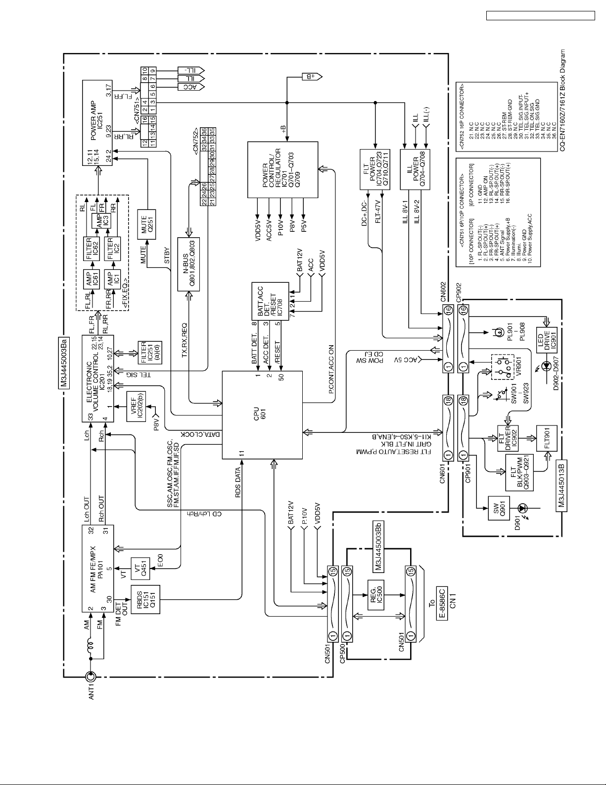
6 BLOCK DIAGRAM (Main / Display / Connector Block)
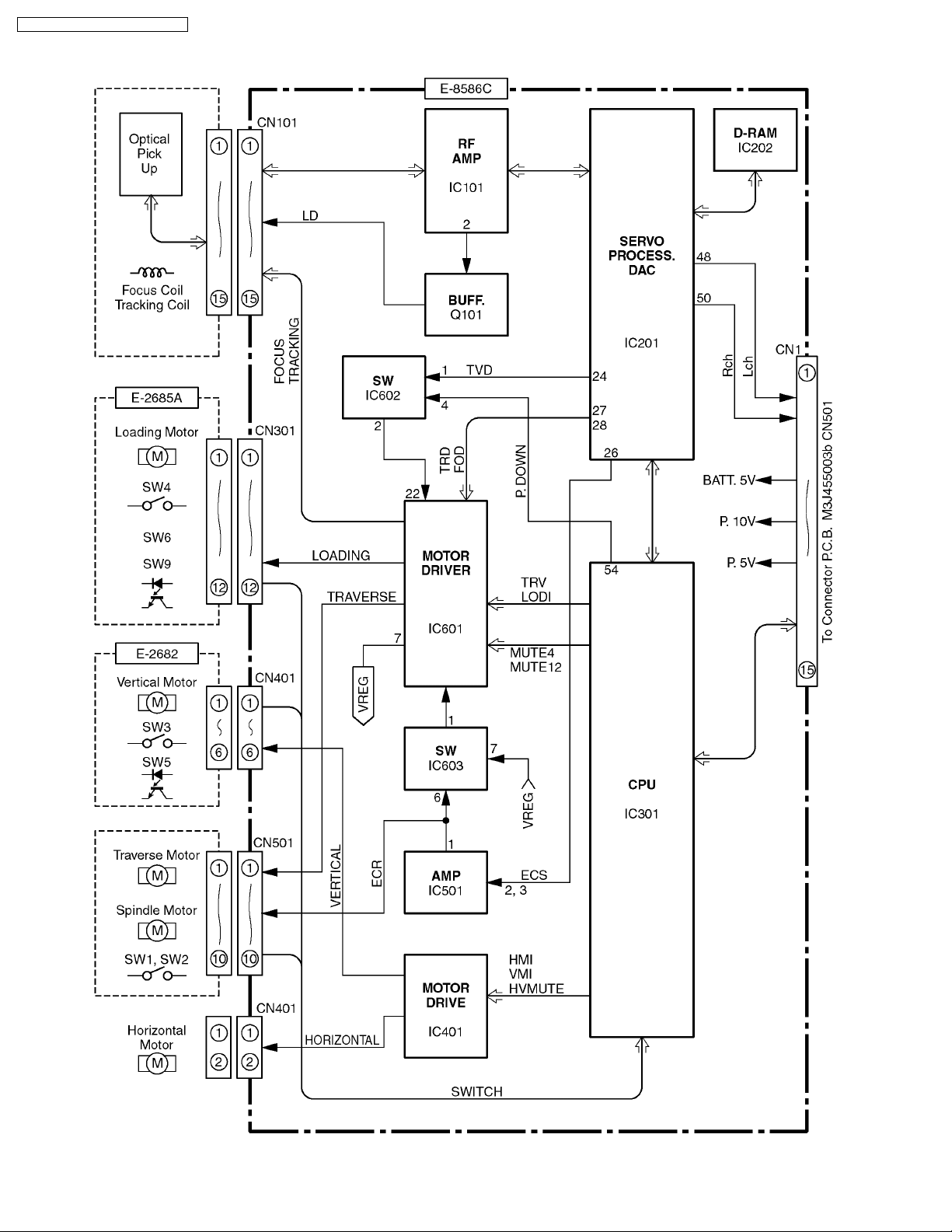
7 BLOCK DIAGRAM (CD Servo Block)
8 TERMINALS DESCRIPTION
9 CD DISC CENTERING ALIGNMENT
10 PACKAGE AND I C BLOCK DIAGRAM 11
2
11 REPLACEM ENT PARTS LIST
3
12 EXPLODED VIEW (Unit)
13 CD CHANGER PARTS LIST
3
4
14 EXPLODE D VIEW (CD Deck-1)
5
15 EXPLODE D VIEW (CD Deck-2)
16 EXPLODE D VIEW (CD Deck-3)
6
7
17 WIRING DIAGRAM
10
18 SCHEMAT IC DIAGRAM
1 FEATUERS
•
•
PLL (Phase Locked Loop) synthesized tuning.
• •
•
•
Preset Scanning / All Preset Scan
• •
•
•
Traffic information and emergency broadcasts
• •
•
•
6-Disc CD changer (in dash board).
• •
•
•
Adjustable VOL, BAS, TRE, FAD and BAL.
• •
•
•
Sttering sheel controls
• •
•
•
Telephone interrupt / audio output
• •
•
•
CQ-EN7160 is Rockford unit. Flat EQ; lowered gain &
• •
Rockford logo on faceplate.
15
20
21
24
25
26
27
33
2 LASER PRODUCTS
2
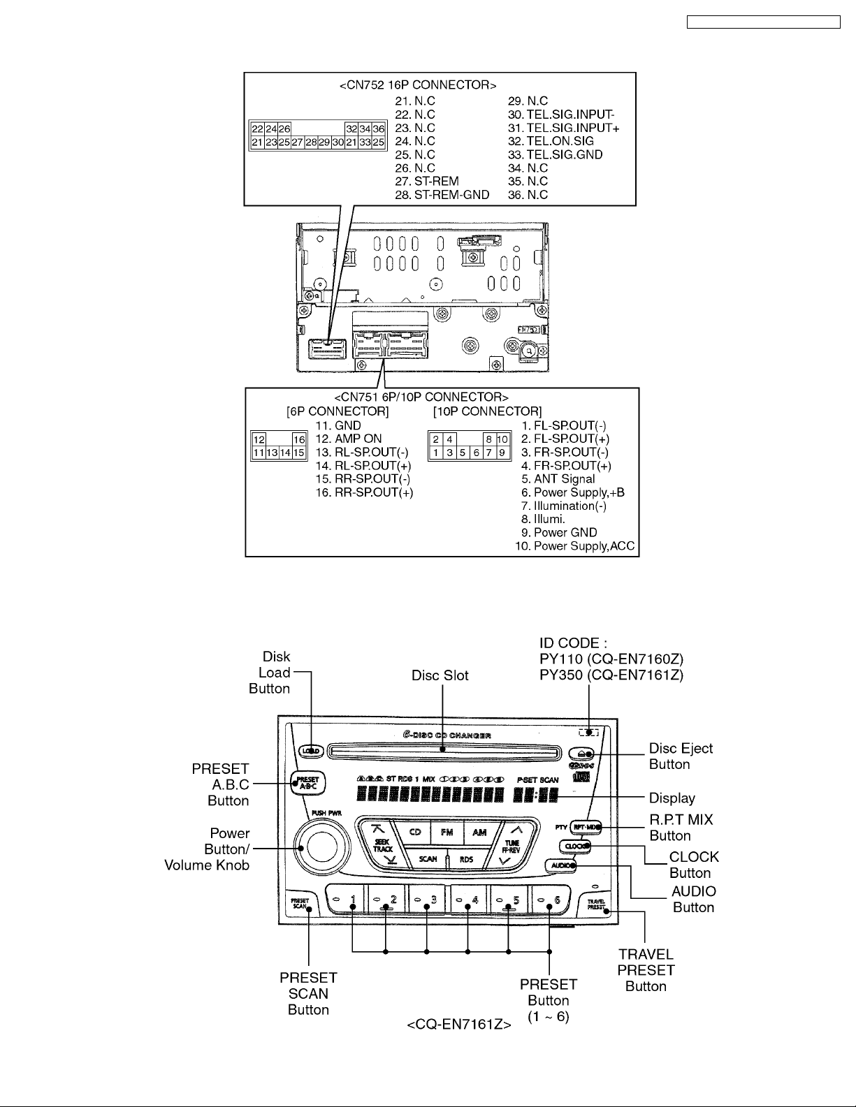
3 REAR VIEW AND CONNECTORS
NISSAN / CQ-EN7160Z / CQ-EN7161Z
4 FRONT VIEW AND FUNCTIONS
3
NISSAN / CQ-EN7160Z / CQ-EN7161Z
5 WIRING CONNECTIONS
4
NISSAN / CQ-EN7160Z / CQ-EN7161Z
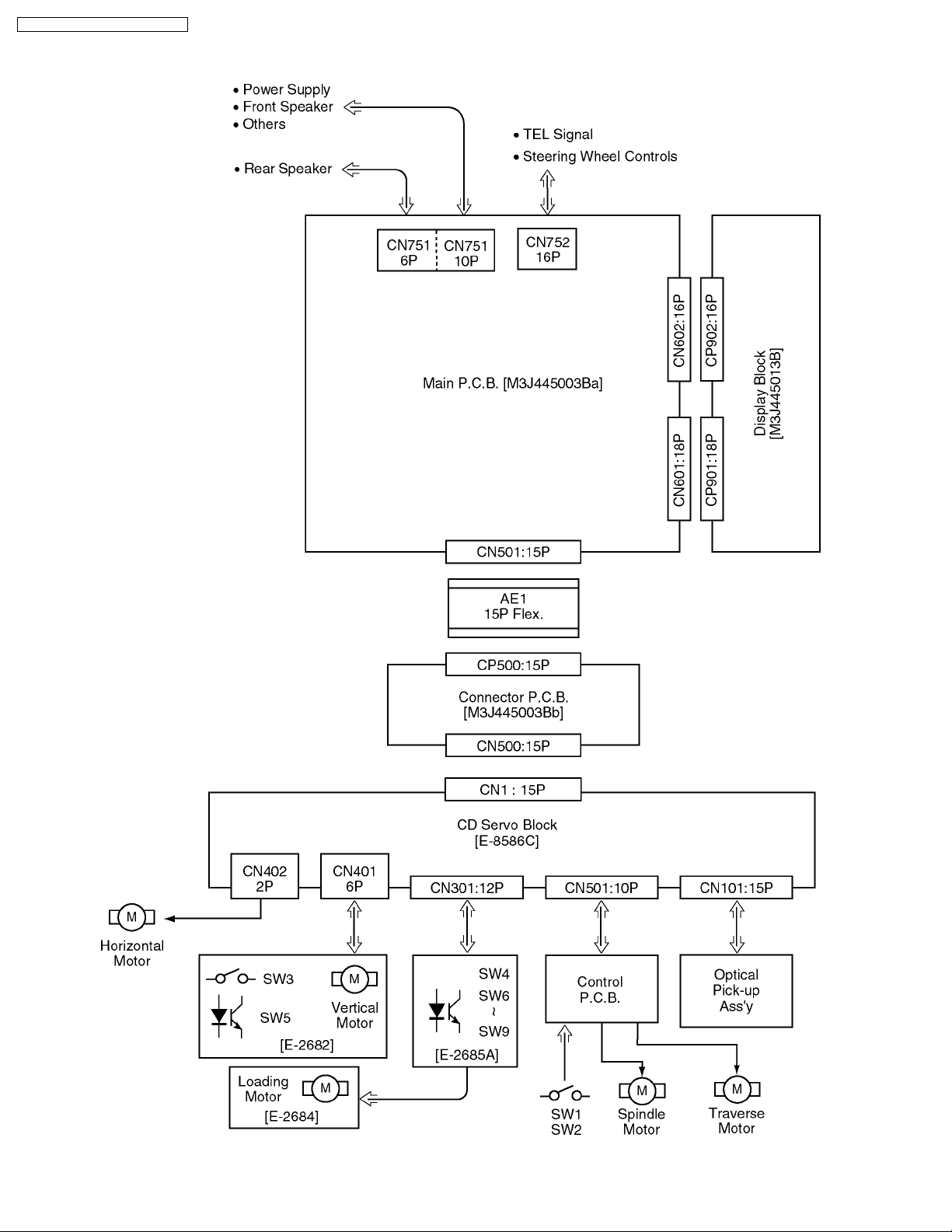
6 BLOCK DIAGRAM (Main / Display / Connector Block)
5
NISSAN / CQ-EN7160Z / CQ-EN7161Z
7 BLOCK DIAGRAM (CD Servo Block)
6
8 TERMINALS DESCRIPTION
8.1. Main Block
IC601 : C2CBBGF000117
Pin
Name Description I/O Vol.(V)
No.
1 BAT-DET Battery level detection I 5.3 5 5
2 ACC-DET ACC level detection I 5.3 5 5.1
3 ANT ON ANT on O 5.4 5.1 0
4 AMP ON AMP on O 5.4 5 5
5 IDC
CONT
6 CD ON LCD illumi. on/off O 5.4 5.1 5.1
7 CD
RESET
8 CD SON CD control I 5.1 4.7 4.7
9 CD SIN CD control O 5.3 5 5
10 CD SCKM CD clock I 5.4 5.1 5.1
11 RDS
DATA
12 NC No connection - - - 13 RDS CLK RDS clock I 2.8 2.5 2.5
14 RADIO
MUTE
15 IDC
MUTE
16 FM CONT FM control O 5.4 0 0
17 AM/FM
CONT
18 VOL CLK Electronic volume clock O 0 0 0
19 VOL
DATA
20 MUTE Not used - 0 0 0
21 STBY Power amp. Stndby O 5.4 5.1 5.1
22 DX/LOC DX/Local O 0 0 0
23 ILL CONT Illumination control I 0 0 0
24 VCONT Security ROM chip select I 0.6 0.7 0
25 ST-REM Stering Wheel control I 5.4 5.1 5.1
26 NC No connection - 0 0 0
27 AVDD +5V power supply - 5.5 5.1 5.1
28 NC No connection - 0 0 0
29 NC No connection - 0 0 0
30 SD Signal detect I 0.4 0 0
31 FM ST FM stereo signal I 0 1.8 0
32 AVSS ACC 5V power switch O 0 0 0
33 REGCPU Not used - 3.4 3.4 3.4
34 VDD +5V power supply - 5.1 5.1 5.1
35 REGOSC REG OSC capacitor - 5.1 5.1 5.1
36 X2 Crystal oscillator terminal - 2.2 2.2 2.2
37 X1 Crystal oscillator terminal - 2.2 2.2 2.2
38 GND Ground - 0 0 0
39 SSC SSC O 0 0 0
40 GND Ground - 0 0 0
41 AM IF AM IF I 0 0 0
42 FN IF FM IF I 0 0 0
43 PLL VDD PLL VDD - 5.1 5.1 5.1
44 FM OSC FM OSC I 2.6 0 0
45 AM OSC AM OSC I 0 1.8 1.9
46 PLL GND Ground - 0 0 0
47 EO0 EO0 O 1.4 1.3 0
48 NC(E01) No connection - - - 49 GND(IC) Ground I 0 0 0
50 RESET Reset input I 5 5 5
51 GRIT IN Grit in I 3.8 3.8 3.8
52 NC No connection - 0 0 0
53 NC No connection - 0 0 0
IDC control O 0 0 0
CD reset O 5.4 5.1 5.1
RDS data I 2.5 3.3 3.3
Radio mute O 0 0 5
IDC mute O 0 0 0
AM/FM control O 5.4 5 0
Electronic volume data O 0 0 0
FM AM CD
NISSAN / CQ-EN7160Z / CQ-EN7161Z
Pin
Name Description I/O Vol.(V)
No.
54 FLT BLK
PWM
55 NC No connection - 0 0 0
56 TEST
POINT
57 NC No connection - 0 0 0
58 NC No connection - 0 0 0
59 BEEP Beep output O 0 0 0
60 NC No connection - 0 0 0
61 PWN PWM O 0 0 0
62 AUTO P Auto Preset O 5 5 5
63 FLT
RESET
64 KS0 Key scan 0 O 0 0 0
65 KS1 Key scan 1 O 0 0 0
66 KS2 Key scan 2 O 0 0 0
67 KS3 Key scan 3 O 0 0 0
68 KS4 Key scan 4 O 0 0 0
69 NC(RX) No connection - 0 0 0
70 NC(TX) No connection - 0 0 0
71 EN A Encoder A I 0 0 0
72 EN B Encoder B I 5.1 5 5
73 KI1 Key return 1 I 5.1 5.1 5.1
74 KI2 Key return 2 I 5.1 5.1 5.1
75 KI3 Key return 3 I 5.1 5.1 5.1
76 KI4 Key return 4 I 5.1 5.1 5.1
77 KI5 Key return 5 I 5 5.1 5.1
78 NC No connection - 0 0 0
79 CD EJ CD disc eject SW I 5.1 5.1 5.1
80 POW SW Power switch I 5.1 5.1 5.1
81 ILL DET Illumination detect I 5 5 5
82 GND Ground - 0 0 0
83 LED LCK LED LCK O 0 0 0
84 LED CLK LED clock O 0 0 0
85 LED
DOUT
86 FLT CS FLT chip select O 4.6 4.8 4.8
87 FLT CP FLT clock O 4.9 5 5
88 FLT DA FLT data O 0 0 0
89 DC-
DC_250H
z
90 P
CONT(AC
C)
91 FLT
CONT
92 ACC ON ACC on O 5 5 5
93 NC Not used - 0 0 0
94 NC Not used - 0 0 0
95 SIYOU Spec 0 I 5.1 5.1 5.1
96 SIYOU1 Spec 1 I 5.1 5.1 5.1
97 SIYOU2 Spec 2 I 5.1 5.1 5.1
98 TEL
ON(EXT)
99 VDD +5V power supply - 5.1 5.1 5.1
100 GND Ground - 0 0 0
FLT PWM O 5 5 5
GA-IN I 5 5 5
FLT reset O 5 5 5
LED data out O 0 0 0
DC-DC control O 5.1 5.1 5.1
Power control O 5.1 5.1 5.1
FLT control O 5 5 5
Spec 3 I 0 0 0
FM AM CD
Note :
Voltage measuerments are with respect to ground, with a
voltmeter (Internal resistance : 10M ohms.)
7
NISSAN / CQ-EN7160Z / CQ-EN7161Z
8.2. Display Block
IC902 : C0HBB0000010
Pin
No.
1 AD3 AD3 O
2 AD4(NC) Not used -
3-37 S1-35 LCD segment data O
38 VDISP1 ’+5V Power Supply 39-56 COM1-18 LCD common I
57-62 COM19-24 Not used -
63 VFL1 FLT voltage -
64 GND ground -
65 OSC0 Oscillator -
66 OSC1 Oscillator -
67 RESET Reset I
68 CS Chip select I
68 CP Clock I
70 DA LCD data I
71 VDD Ground 72-75 P1-4 Not used -
76 VFL2 FLT voltage -
77 NC Not used -
78 VDISP2 ’+5V Power Supply -
79,80AD1, 2 FLT AD O
Port Description I/O
8.3. CD Servo Block
IC201 : MN662783RPW
Pin No. Port Description I/O (V)
1 VDD +5V power supply - 5.0
2 D0 D-RAM data I/O 2.3
3 D1 D-RAM data I/O 1.8
4 /WE D-RAM data write O 4.9
5 /RAS D-RAM row address strobe O 3.4
6 D2 D-RAM data I/O 0.8
7 D3 D-RAM data I/O 0
8 /CAS0 D-RAM columun address strobe O 3.9
9 /CAS1 D-RAM columun address strobe O 0
10 A8 D-RAM address O 0.6
11 A7 D-RAM address O 1.1
12 A6 D-RAM address O 0.7
13 A5 D-RAM address O 0
14 A4 D-RAM address O 1.1
15 A9 D-RAM address O 0.4
16 A0 D-RAM address O 1.0
17 A1 D-RAM address O 1.0
18 A2 D-RAM address O 1.0
19 A3 D-RAM address O 0
20 VSS2 Ground - 0
21 VDD2 +5V power supply - 5.0
22, 23 - Not used - -
24 TVD Traverse motor control O 2.5
25 PC Not used - 26 ECS Spindle motor control O 2.4
27 TRD Tracking coil drive O 2.5
28 FOD Focus coil drive O 2.4
29 FBAL Focus balance O 1.9
30 TBAL Tracking balance O 3.0
31 VREF Reference voltage I 2.5
32 FE Focus error I 2.5
33 TE Tracking error I 2.5
34 RFENV RF envelope I 2.5
35 OFT Off track signal I 0
36 /RFDET RF detecting signal I 0
37 BDO Drop-out signal I 0
38 LDON Laser on signal O 4.5
39 ARF RF signal I 2.5
40 IREF Reference current input I 1.2
41 DRF Biase for DSL I 2.4
42 DSLF Loop filter for DSL I/O 2.5
43 SDLF2 Loop filter for DSL I/O 2.2
44 PLLF Loop filter for PLL I/O 1.4
45 VCOF Not used - 46 AVDD2 +5V power supply - 5.0
47 AVSS2 Ground - 0
48 OUTL L channel output O 2.3
49 AVSS1 Ground - 0
50 OUTR R channel output O 2.3
51 AVDD1 +5V power supply - 4.7
52-54 - (Connecting to ground) - 0
55 FLAG Flag output O 0
56 FCLK Frame clock O 0
57-59 - Not used - -
60 TX Not used - 61 MCLK Clock for I/F command I 1.0
62 MDATA Data for I/F command I 3.1
63 MLD I/F command load I 5.0
64 BLKCK Subcode block clock O 0
65 SQCK Ext. clock for sub code-Q I 5.0
66 SUBQ Code for sub. code-Q O 3.8
67 DMUTE Mute input I 0
68 STAT Status signal O 5.0
69 /RST Reset input I 5.0
70 CSEL (Connecting to ground) - 0
71 PMCK PM clock O 2.5
72 SMCK SM clock O 2.5
73 SUBC Serial data of sub code O 0
74 SBCK Shift clock for SUBC I 0.6
75 /CLDCK Not used - 76 /TEST (Connecting to VDD) - 5.0
77 X1 Crystal oscillator - 0.4
78 X2 Crystal oscillator - 3.2
79 VDD1 +5V power supply - 5.0
80 VSS1 Ground - 0
IC301 : MN1873260AB4
Pin
No.
1 VDD +5V power supply - 5.0
2 OSC2 Crystal oscillator - 2.2
3 OSC1 Crystal oscillator - 2.1
4 VSS Ground - 0
5 XI (Connecting to ground) - 0
6 XO Not used - 7 CM (Connecting to ground) - 0
8 VREFH Reference voltage I 5.0
9 SW13 Shuter SW I 4.9
10 SW12 Horizontal origin I 4.9
11 SW11 Clump SW I 0
12 SW10 Play SW I 0
13 SW4 Shuter SW I 4.9
14 SW3 Tray origin SW I 0
15 SW2 Inner SW I 4.8
16 SW1 Outer SW I 4.9
17 VREFL Reference voltage I 0
18 /RESET Reset input I 4.9
19 - (Ground pull-down) - 0
20 SCKM Clock for serial data I 5.0
21 SIM CD changer serial data I 1.3
22 SOM CD changer serial data O 4.3
23 SQCK Ext. clock for sub. code-Q O 5.0
Port Description I/O (V)
8
24 SUBQ Code for sub. code-Q I 1.6
25 - Not used - 5.0
26 - (Ground pull-down) - 0
27 CD.ON CD changer start/stop I 5.0
28 - Not used - 5.0
29 BLKCK Sub. code block clock I 0
30 P.ON Not used - 5.0
31 MUTE Mute output O 5.0
32 - (Ground pull-down) - 0
33 SENS Servo status O 0
34 CLVS Servo status O 5.0
35 FLOCK Focus servo lock O 0.2
36 TLOCK Tracking servo lock O 0
37 VMI Horizontal motor control O 2.5
38 HMI Vertical motor control O 0
39 HVMUTE H/V motor mute O 0
40-42 - (Ground pull-down) - 0
43 SW9 Disc-in (B) SW I 0
44 SW8 Disc-in (L) SW I 0
45 SW7 Disc-in (F) SW I 0
46 SW6 Disc push SW I 0
47 SW5 Tray hight SW I 4.5
48 BDO Drop-out signal I 0
49 DQSY Not used - 50 /RST Reset output O 5.0
51 STAT Status signal I 2.1
52 DMUTE Mute output O 0
53 XE Not used - 54 P.DOWN Power down signal O 0
55 - No connection - 56 MLD I/F command load O 5.0
57 MDATA Data for I/F command O 3.1
58 MCLK Clock for I/F command O 4.1
59 SPMT Spindle mute O 5.0
60 MUTE12 Focus/Tracking mute O 0
61 MUTE4 Loading motor mute O 4.8
62 LDOI Loading motor control I/O 2.5
63 TRV Forced traverse control I/O 2.4
64 SYNC Not used - -
NISSAN / CQ-EN7160Z / CQ-EN7161Z
9
NISSAN / CQ-EN7160Z / CQ-EN7161Z
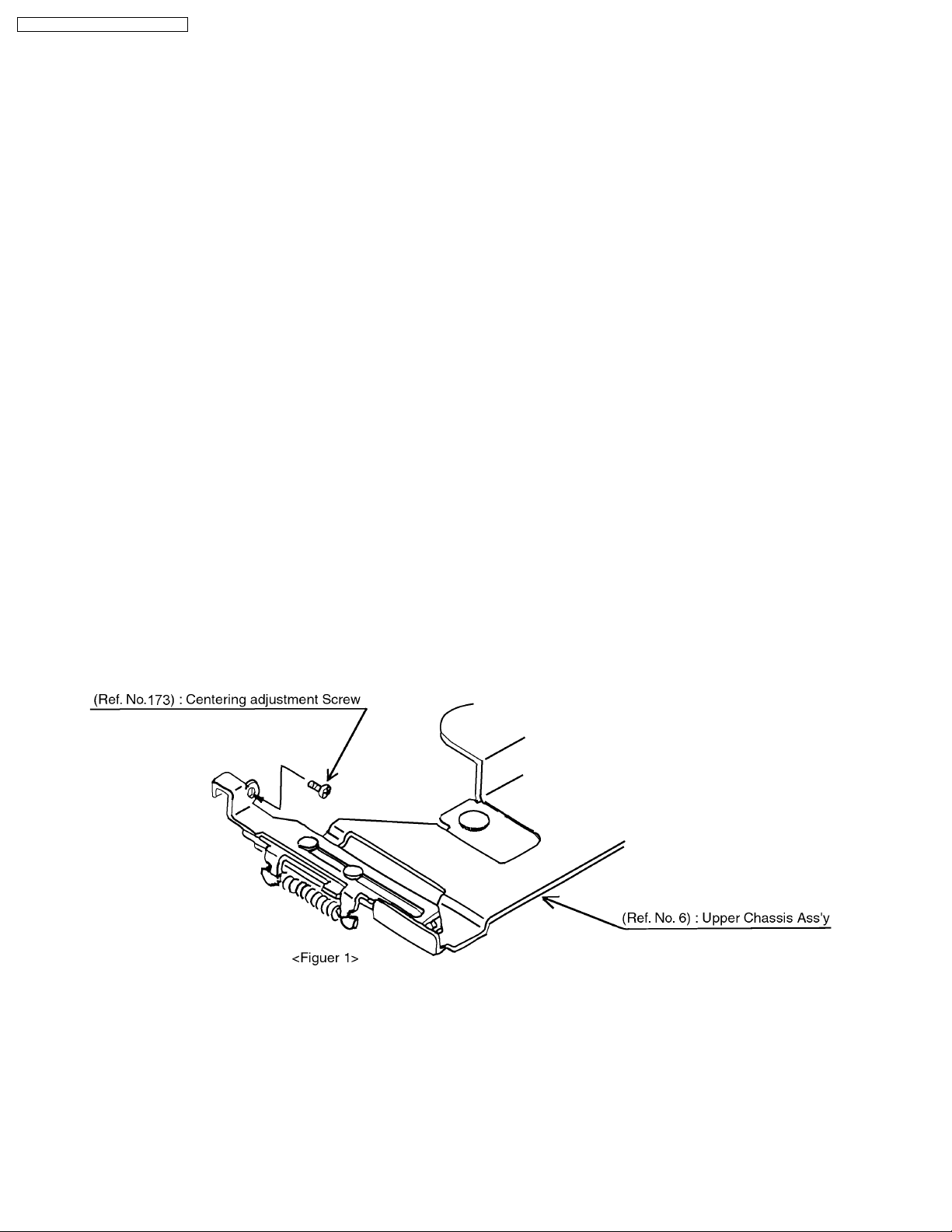
9 CD DISC CENTERING ALIGNMENT
•
•
This adjustment is for assuring that compact discs will be placed in the center of the turntable.
• •
<Adjustment Condition / Jig>
•
•
Power Supply Voltage : 13.2V
• •
•
•
Test Disc : TCD-792A
• •
<Adjustment Procedures>
1. Attach the adjusting screw to the upper chassis (See Figure 1.).
2. Insert the test CD (TCD-792A) into the disc No.1 position and play it.
3. After checking whether the disc is centered on the turntable, turn the adjusting screw unit it is in the center.
<Check Items>
•
•
Check that the disc is correctly centered.
• •
•
•
Check that the disc is securely clamped.
• •
•
•
Check that no abnormal noise is produced when clamping the disc.
• •
[Directions of Turning the Adjusting Screw]
•
•
CD stops before its proper position : Turn the screw counterclockwise.
• •
•
•
CD overruns : Turn the screw clockwise.
• •
4. After the adjustment, lock the screw.
10
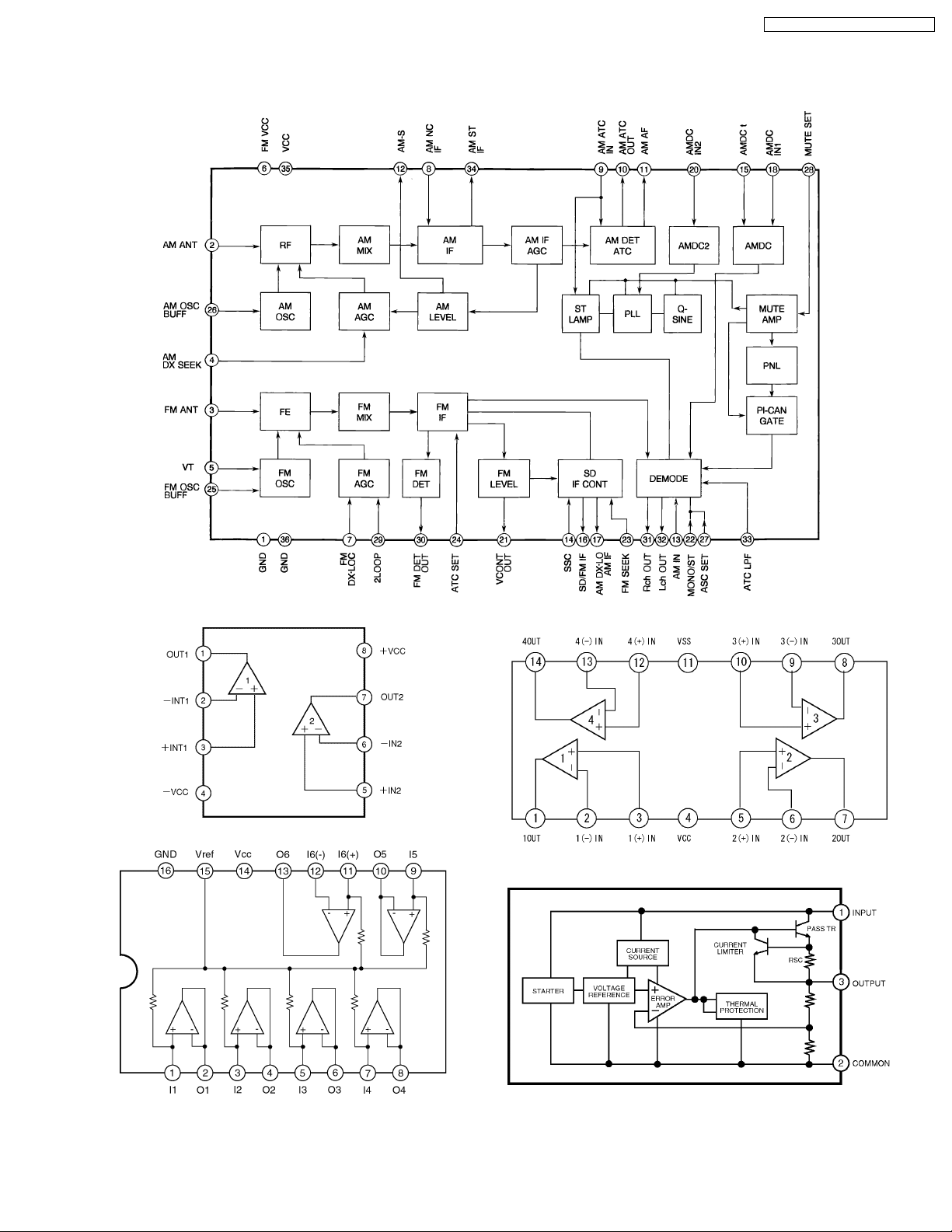
10 PACKAGE AND IC BLOCK DIAGRAM
10.1. Main Block
NISSAN / CQ-EN7160Z / CQ-EN7161Z
IC1, 3, 61 : YEAMPC4570E1
PA101 : YMP0PTA514B0
IC202 : C0ABCB000032
IC2, 62 : YEAMTA2062FL
IC500 : AN78N05
11
 Loading...