

Page 1
查询NTK3043N供应商
NTMD4102PR2
Product Preview
Trench Power MOSFET
-20 V, P-Channel, SO-8 Dual
This P-Channel device was designed using ON Semiconductor’s
leading edge trench technology for low R
SO-8 dual package for high power and current handling capability.
The low R
performance is particularly suited for game systems,
DS(on)
notebook and desktop computers, and printers.
Features & Benefits
• Leading -20 V Trench for Low R
DS(on)
• SO-8 Package Provides Excellent Thermal Performance
• Surface Mount SO-8 Package Saves Board Space
• Pb Free Package for Green Manufacturing
performance in the
DS(on)
R
DS(on)
R
DS(on)
http://onsemi.com
V
BR(DSS)
= -20 VOLTS
(max) = 19 m @ -10 V
I
D(max)
(Note 1) = -8.5 A
(max) = 30 m @ -4.5 V
I
D(max)
(Note 1) = -6.5 A
Applications
• Load/Power Management
• Battery Switching for Multi Cell Li-Ion
• Buck-Boost Synchronous Rectification
MAXIMUM RATINGS (T
Rating Symbol Value Unit
Drain-to-Source Voltage V
Gate-to-Source Voltage V
Drain Current
- Continuous @ T
- Pulsed Drain Current (t = 10 µs)
Steady State Power Dissipation
@ T
= 25°C (Note 1)
A
Operating Junction and Storage Temperature
Range
Continuous Source Current (Body Diode) I
Lead Temperature for Soldering Purposes
(1/8″ from case for 10 seconds)
THERMAL RESISTANCE RATINGS
Thermal Resistance
- Junction- to- Ambient - Steady State (Note 1)
- Junction-to-Ambient - t ≤ 10 s (Note 1)
- Junction-to-Lead - Steady State (Note 2)
1. Surface-mounted on FR4 board using 1″ sq pad size (Cu area = 1.127 in sq
[1 oz] including traces)
2. Surface-mounted on FR4 board using the minimum recommended pad size
(Cu area = TBD in sq)
This document contains information on a product under development. ON Semiconductor
reserves the right to change or discontinue this product without notice.
= 25°C unless otherwise noted)
A
= 25°C (Note 1)
A
DSS
I
I
DM
P
TJ, T
T
R
R
R
GS
-20 V
±20 V
A
°C
°C/W
D
stg
L
JA
JA
JL
-6.5
-30
1.1 W
-55 to
150
-0.9 A
260 °C
TBD
TBD
TBD
D
S
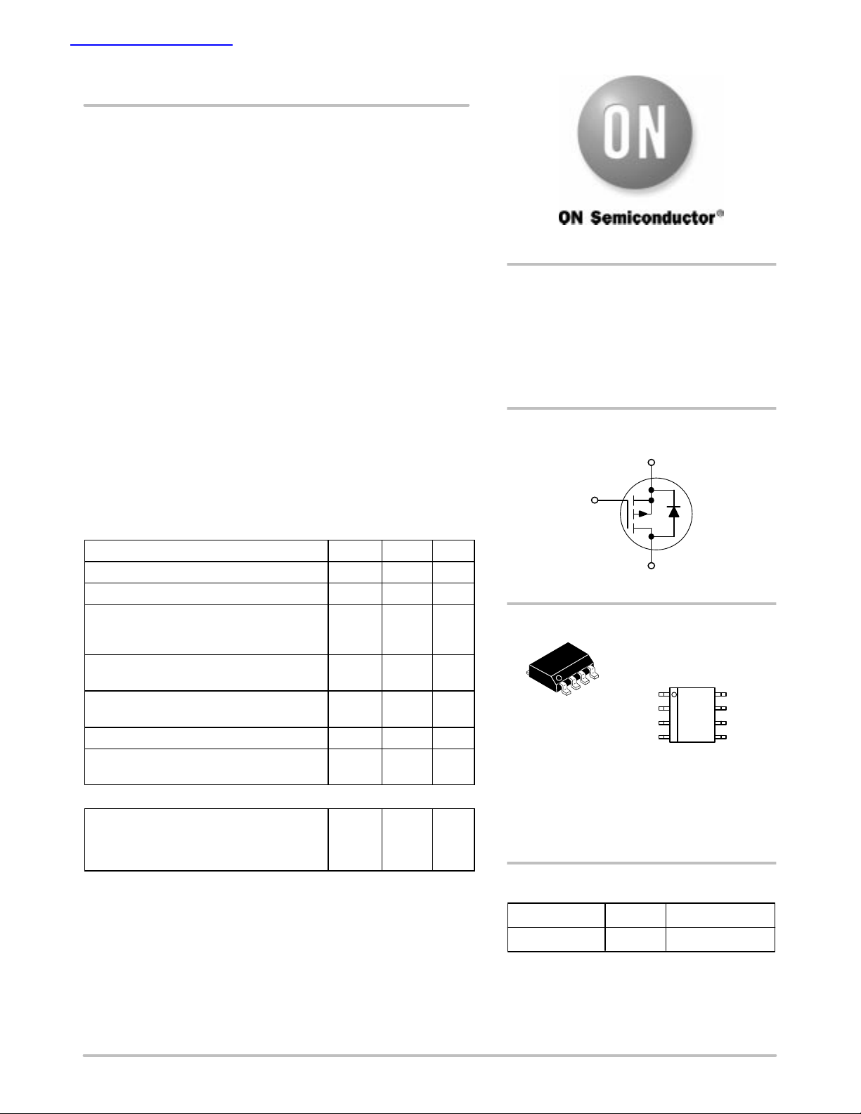
P-Channel MOSFET
S
G
D
MARKING DIAGRAM &
PIN ASSIGNMENT
8
SO-8
CASE 751
STYLE 12
Source-1
1
Gate-1
Source-2
Gate-2
XXX = Specific Device Code
A = Assembly Location
L = Wafer Lot
Y = Year
W = Work Week
18
XXXXXX
ALYW
Top View
Drain-1
Drain-1
Drain-2
Drain-2
ORDERING INFORMATION
Device Package Shipping
NTMD4102PR2 SO-8 2500/Tape & Reel
Semiconductor Components Industries, LLC, 2003
March, 2003 - Rev. 0
1 Publication Order Number:
NTMD4102PR2/D
Page 2
NTMD4102PR2
)
V
S
V)
(V
GS
5 V, V
DS
)
dISD/dt
100 A/s, I
A)
ELECTRICAL CHARACTERISTICS (T
= 25°C unless otherwise noted)
A
Characteristic Symbol Min Typ Max Unit
OFF CHARACTERISTICS
Drain-to-Source Breakdown Voltage (Note 3)
= 0 V, ID = 250 A)
(V
GS
Zero Gate Voltage Drain Current (Note 3)
(V
= 0 V, VDS = -16 V)
GS
Gate-to-Source Leakage Current
(V
= ±20 V, VDS = 0 V)
GS
ON CHARACTERISTICS
Gate Threshold Voltage (Note 3)
= VDS, ID = -250 A)
(V
GS
Drain-to-Source On-Resistance
(V
= -10 V, ID = -8.5 A)
GS
= -4.5 V, ID = -6.5 A)
(V
GS
Forward Transconductance (VDS = -10 V, ID = -8.4 A) g
CHARGES, CAPACITANCES & GATE RESISTANCE
Input Capacitance
Output Capacitance
Reverse Transfer Capacitance
(VGS = 0 V, f = 1 MHz,
= -10
V
= -10 V
D
Total Gate Charge (VGS = -4.5 V, VDS = -10 V,
I
= -8.4 A)
D
Threshold Gate Charge (VGS = -4.5 V, VDS = -10 V,
= -8.4 A)
I
D
Gate-to-Source Gate Charge (VDS = -10 V, ID = -8.4 A) Q
Gate-to-Drain “Miller” Charge (VDS = -10 V, ID = -8.4 A) Q
Output Charge (VDS = -10 V, VGS = 0 V) Q
Gate Resistance R
SWITCHING CHARACTERISTICS (Note 4)
Turn-On Delay Time
Rise Time
Turn-Off Delay Time
(VGS = -4.5 V, VDS = -10 V,
4.
I
= -1.0 A, RG = 6.0 Ω)
D
10 V,
Fall Time t
DRAIN-SOURCE DIODE CHARACTERISTICS
Forward Diode Voltage
(VGS = 0 V, ISD = -1.7 A) V
Reverse Recovery Time
Charge Time
(VGS = 0 V, VDS = -10 V,
dI
/dt = 100 A/s, I
=
= -1.7 A
= -1.7
SD
Discharge Time
Reverse Recovery Charge Q
3. Pulse Test: Pulse Width ≤300 µs, Duty Cycle ≤ 2%.
4. Switching characteristics are independent of operating junction temperature.
V
(BR)DSS
I
DSS
I
GSS
V
GS(th)
R
DS(on)
C
C
C
Q
G(tot)
Q
G(th)
OSS
t
d(on)
t
d(off)
t
FS
iss
oss
rss
GS
GD
t
SD
rr
t
a
t
b
-20 - - V
- - -1.0 A
- - ±100 nA
-1.0 - - V
m
-
-
TBD
TBD
19
30
- TBD - S
- TBD - pF
- TBD -
- TBD -
- TBD TBD nC
- TBD TBD nC
- TBD - nC
- TBD - nC
- TBD - nC
G
r
- TBD -
- TBD -
- TBD -
ns
- TBD -
f
- TBD -
- TBD TBD V
- TBD TBD ns
- TBD - ns
- TBD - ns
rr
- TBD - nC
http://onsemi.com
2
Page 3
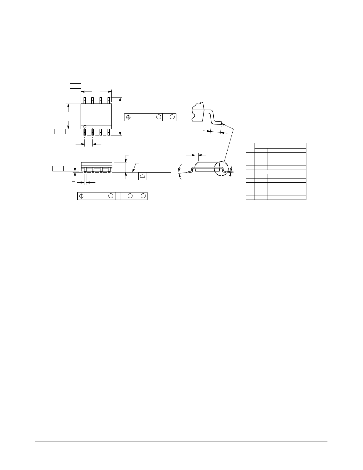
-Z-
-Y-
NTMD4102PR2
PACKAGE DIMENSIONS
SOIC-8 NB
CASE 751-07
ISSUE AA
NOTES:
-XA
58
B
1
S
0.25 (0.010)
4
M
M
Y
K
G
C
SEATING
PLANE
0.10 (0.004)
H
D
0.25 (0.010) Z
M
Y
SXS
N
X 45
M
1. DIMENSIONING AND TOLERANCING PER ANSI
Y14.5M, 1982.
2. CONTROLLING DIMENSION: MILLIMETER.
3. DIMENSION A AND B DO NOT INCLUDE MOLD
PROTRUSION.
4. MAXIMUM MOLD PROTRUSION 0.15 (0.006) PER
SIDE.
5. DIMENSION D DOES NOT INCLUDE DAMBAR
PROTRUSION. ALLOWABLE DAMBAR
PROTRUSION SHALL BE 0.127 (0.005) TOTAL IN
EXCESS OF THE D DIMENSION AT MAXIMUM
MATERIAL CONDITION.
6. 751−01 THRU 751−06 ARE OBSOLETE. NEW
STANDARD IS 751−07.
MILLIMETERS
DIMAMIN MAX MIN MAX
4.80 5.00 0.189 0.197
B 3.80 4.00 0.150 0.157
C 1.35 1.75 0.053 0.069
D 0.33 0.51 0.013 0.020
G 1.27 BSC 0.050 BSC
H 0.10 0.25 0.004 0.010
J
J 0.19 0.25 0.007 0.010
K 0.40 1.27 0.016 0.050
M 0 8 0 8
N 0.25 0.50 0.010 0.020
S 5.80 6.20 0.228 0.244
STYLE 12:
PIN 1. SOURCE
2. SOURCE
3. SOURCE
4. GATE
5. DRAIN
6. DRAIN
7. DRAIN
8. DRAIN
INCHES
http://onsemi.com
3
Page 4

NTMD4102PR2
ON Semiconductor and are registered trademarks of Semiconductor Components Industries, LLC (SCILLC). SCILLC reserves the right to make
changes without further notice to any products herein. SCILLC makes no warranty, representation or guarantee regarding the suitability of its products for any
particular purpose, nor does SCILLC assume any liability arising out of the application or use of any product or circuit, and specifically disclaims any and all
liability, including without limitation special, consequential or incidental damages. “Typical” parameters which may be provided in SCILLC data sheets and/or
specifications can and do vary in different applications and actual performance may vary over time. All operating parameters, including “Typicals” must be
validated for each customer application by customer’s technical experts. SCILLC does not convey any license under its patent rights nor the rights of others.
SCILLC products are not designed, intended, or authorized for use as components in systems intended for surgical implant into the body, or other applications
intended to support or sustain life, or for any other application in which the failure of the SCILLC product could create a situation where personal injury or death
may occur. Should Buyer purchase or use SCILLC products for any such unintended or unauthorized application, Buyer shall indemnify and hold SCILLC
and its officers, employees, subsidiaries, affiliates, and distributors harmless against all claims, costs, damages, and expenses, and reasonable attorney fees
arising out of, directly or indirectly, any claim of personal injury or death associated with such unintended or unauthorized use, even if such claim alleges that
SCILLC was negligent regarding the design or manufacture of the part. SCILLC is an Equal Opportunity/Affirmative Action Employer.
PUBLICATION ORDERING INFORMATION
Literature Fulfillment:
Literature Distribution Center for ON Semiconductor
P.O. Box 5163, Denver, Colorado 80217 USA
Phone: 303-675-2175 or 800-344-3860 Toll Free USA/Canada
Fax: 303-675-2176 or 800-344-3867 Toll Free USA/Canada
Email: ONlit@hibbertco.com
N. American Technical Support: 800-282-9855 Toll Free USA/Canada
http://onsemi.com
JAPAN: ON Semiconductor, Japan Customer Focus Center
2-9-1 Kamimeguro, Meguro-ku, Tokyo, Japan 153-0051
Phone: 81-3-5773-3850
ON Semiconductor Website: http://onsemi.com
For additional information, please contact your local
Sales Representative.
NTMD4102PR2/D
4
 Loading...