

NCP5603
High Efficiency Charge Pump
Converter
The NCP5603 is an integrated circuit dedicated to the medium
power White LED applications. The power conversion is achieved by
means of a charge pump structure, using two external ceramic
capacitors, making the system extremely tiny. The device supplies a
constant voltage to the load from a low battery voltage source. It is
particularly suited for the High Efficiency LED used in low cost, low
power applications, with high extended battery life.
Features
•Wide Battery Supply Voltage Range: 2.7 < V
•Automatic Operating Mode 1X, 1.5X and 2X Improves Efficiency
•Dimmable Output Current
•Up to 350 mA Output Pulsed Current
•Selectable Output Voltage
•High Efficiency Up To 90%
•Supports 2.5 kV ESD, Human Body Model
•Supports 200 V Machine Model ESD
•Low 40 mA Short Circuit Current
•Pb-Free Package is Available
< 5.5 V
CC
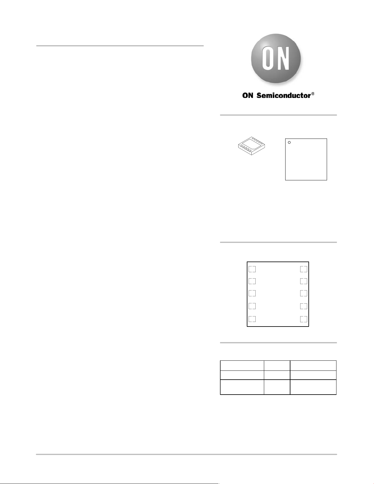
http://onsemi.com
MARKING
DIAGRAM
5603
DFN10, 3x3
MN SUFFIX
CASE 485C
5603 = Specific Device Code
A = Assembly Location
L = Wafer Lot
Y = Year
W = Work Week
G = Pb-Free Package
(Note: Microdot may be in either location)
ALYWG
G
Applications
•High Power LED
•Back Light Display
•High Power Flash
PIN CONNECTIONS
C2P
V
1
out
2
C1P
V
3
bat
Fsel
4
Vsel
5
(Top View)
ORDERING INFORMATION
Device Package Shipping
NCP5603MNR2 DFN10 3000/ Tape & Reel
NCP5603MNR2G
†For information on tape and reel specifications,
including part orientation and tape sizes, please
refer to our Tape and Reel Packaging Specification
Brochure, BRD8011/D.
DFN10
(Pb-Free)
10
9
C1N
GND
8
7
C2N
EN
6
†
3000/ Tape & Reel
© Semiconductor Components Industries, LLC, 2007
July, 2007 - Rev. 2
1 Publication Order Number:
NCP5603/D

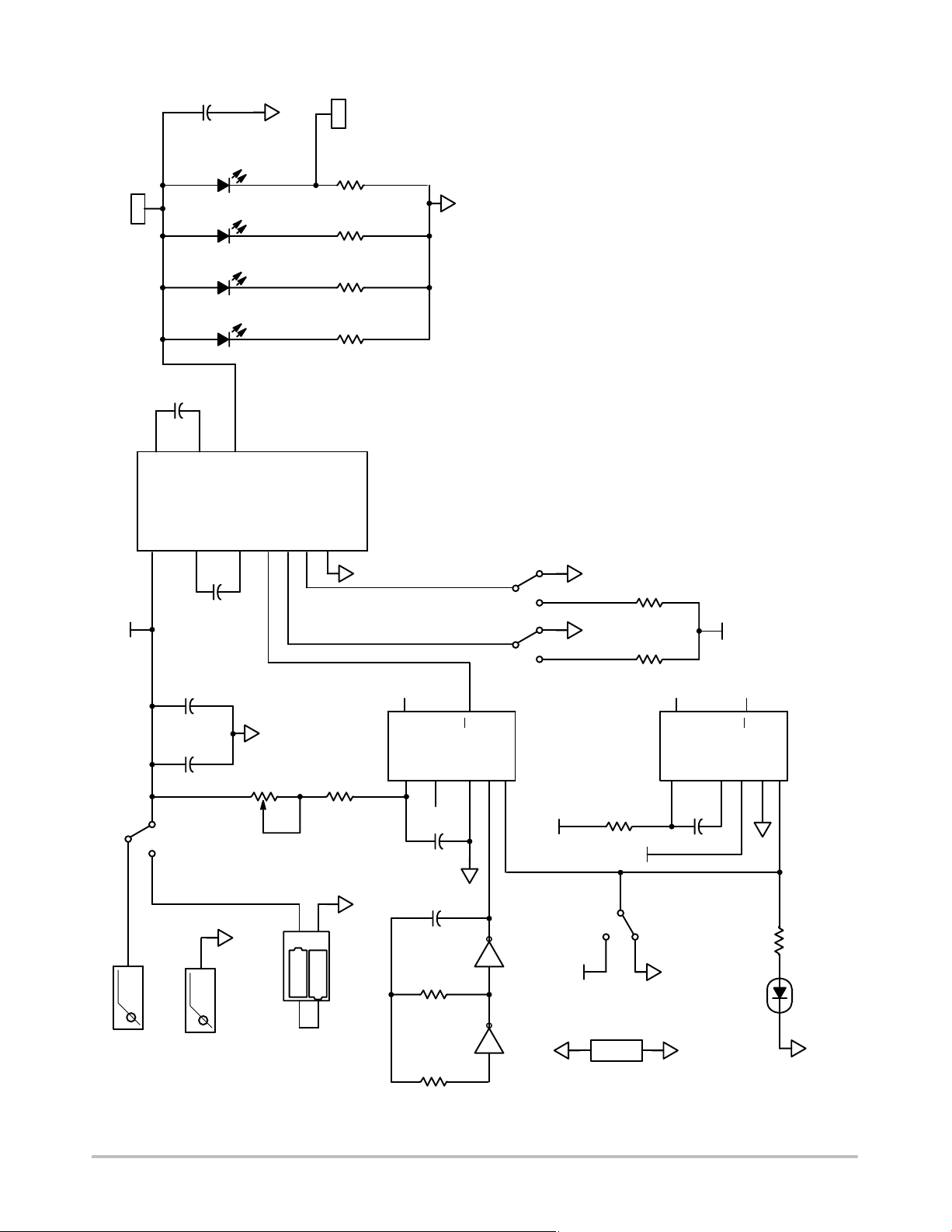
GND
C3
4.7 mF/16 V
1 mF/16 V
PWM
FSEL
VSEL
NCP5603
V
bat
U1
3
V
C1
GND
2
C1P
9
C1N
6
EN/PWM
4
Fsel
5
Vsel
8
GND
bat
NCP5603
C2N
C2P
V
out
7
10
1
D1
C2
1 mF/16 V
LWT67C
D2
C4
1 mF/16 V
LWT67C
D3
GND
LWT67C
LWT67C
D4
R1
10 W
Figure 1. Typical Application
R2
10 W
GND
R3
R4
10 W
10 W
http://onsemi.com
2

NCP5603
V
bat
3
V
bat
Fsel
Vsel
V
bat
10
C2P
7
C2N
Thermal Shutdown
9
C1N
V
bat
POWER SWITCHES
2
C1P
LEVEL SHIFTER AND MOSFET DRIVE
CONTROL
4
GND
V
bat
V
out
1
V
out
LOGIC AND ANALOG
5
-
+
EN
6
GND
BANDGAP
GND
8
GND
Figure 2. Block Diagram
http://onsemi.com
3

NCP5603
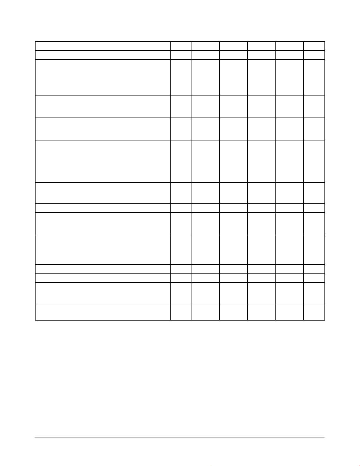
PIN FUNCTION DESCRIPTION
Pin Symbol Type Description
1 V
out
2 C1N POWER One side of the external charge pump capacitor (C
3 V
bat
4 Fsel INPUT, Digital This pin is used to program the operating frequency:
5 Vsel INPUT, Digital This pin setup the output voltage:
6 EN/PWM INPUT, Digital This pin controls the activity of the NCP5603 chip:
7 C2N POWER One side of the external charge pump capacitor (C
8 GND GROUND This pin combines the Signal ground and the Power ground and must be connected to the
9 C1P POWER One side of the external charge pump capacitor (C
10 C2P POWER One side of the external charge pump capacitor is connected to this pin, associated with
1. Using ceramic 16 V working voltage capacitors is recommended to compensate the DC bias effect encountered with such type of capacitors.
2. Any external impedance connected to pin 6 shall be 10 kW or higher.
OUTPUT, PWR This pin supplies the regulated voltage to the external LED. Since high current transients
are present in this pin, care must be observed to avoid voltage spikes in the system. Good
high frequency layout technique must be observed.
) is connected to this pin, associated
FLY
with C1P, pin 9. Using low ESR ceramic capacitor is recommended to optimize the Charge
Pump efficiency.
POWER This pin shall be connected to the power source, and must be decoupled to Ground by a
low ESR capacitor (2.2 mF/6.3 V ceramic or better (see Note 1)).
Fsel = 0 → Fop = 262 kHz
Fsel = 1 → Fop = 650 kHz
Vsel = 0 → V
Vsel = 1 → V
= 4.5 V
out
= 5.0 V
out
EN/PWM = Low → the chip is deactivated, the load is disconnected
EN/PWM = High → the chip is activated and the load is connected to the
regulated output current.
The NCP5603 can operate either in a continuous mode (EN/PWM = High), or can be
controlled by a PWM pulse applied to EN/PWM to dim the output light. When EN/PWM is
Low, the external load is disconnected from the converter, providing a very low standby
current. The pull down built-in resistance makes sure the chip is deactivated even if the
EN/PWM pin is disconnected (see Note 2).
) is connected to this pin, associated
FLY
with C2P, pin 10. Using low ESR ceramic capacitor is recommended to optimize the
Charge Pump efficiency.
system ground. Using good quality ground plane is mandatory to avoid spikes on the logic
signal lines.
) is connected to this pin, associated
FLY
with C1N, pin 2. Using low ESR ceramic capacitor is recommended to optimize the Charge
Pump efficiency.
C2N, pin 7. Using low ESR ceramic capacitor is recommended to optimize the Charge
Pump efficiency.
http://onsemi.com
4

NCP5603
MAXIMUM RATINGS
Rating Symbol Value Unit
Power Supply Voltage V
Power Supply Current I
Digital Input Pins V
bat
bat
in
-0.5 V < Vbat < Vbat +0.5 V < 6.0 V V
Digital Input Pins Iin "5.0 mA
Output Voltage V
ESD Capability (Note 3)
Human Body Model
V
out
ESD
Machine Model
DFN10, 3x3 Package
Power Dissipation @ Tamb = +85°C
Thermal Resistance, Junction-to-Air (R
)
q
JA
Operating Ambient Temperature Range T
Operating Junction Temperature Range T
Maximum Junction Temperature T
Storage Temperature Range T
P
R
Jmax
q
stg
DS
JA
A
J
Latchup Current Maximum Rating 100 mA per JEDEC standard, JESD78
Moisture Sensitivity Level (MSL) 1 per IPC/JEDEC standard, J-STD-020A
Stresses exceeding Maximum Ratings may damage the device. Maximum Ratings are stress ratings only. Functional operation above the
Recommended Operating Conditions is not implied. Extended exposure to stresses above the Recommended Operating Conditions may affect
device reliability.
3. This device series contains ESD protection and exceeds the following tests:
Human Body Model (HBM) "2.5 kV per JEDEC Standard: JESD22-A114
Machine Model (MM) "200 V per JEDEC Standard: JESD22-A115.
4. The maximum package power dissipation limit must not be exceeded.
7.0 V
800 mA
5.5 V
2.5
kV
200
580
68.5
mW
°C/W
-40 to +85 °C
-40 to +125 °C
+150 °C
-65 to +150 °C
V
http://onsemi.com
5
NCP5603
ELECTRICAL CHARACTERISTICS @ 2.85 V < Vbat < 5.5 V (-40°C to +85°C ambient temperature, unless otherwise noted).
Characteristic
Power Supply 3 V
Quiescent Current @ V
= 3.7 V, I
bat
out
= 0 mA
@ Pulsed Clock Fop = 262 kHz
@ Pulsed Clock Fop = 650 kHz
@ Continuous Clock Fop = 262 kHz
@ Continuous Clock Fop = 650 kHz
Shutdown Current @ I
@ 2.85 < V
@ V
bat
bat
= 5.5 V
< 4.2 V
= 0 mA, EN/PWM = L
out
Output Voltage Regulation
@ Vsel = 1, 2.85 V < V
@ Vsel = 0, 2.85 V < V
< 4.3 V
bat
< 4.3 V
bat
Continuous DC Load Current (Note 7)
Cin = 1.0 mF, C
@ Vsel = 1, 3.2 V < V
@ Vsel = 0, 3.2 V < V
@ Vsel = 1, 2.85 V < V
@ Vsel = 0, 2.85 V < V
= 1.0 mF, Cout = 1.0 mF
FLY
< 4.3 V
bat
< 4.3 V
bat
bat
bat
< 4.3 V
< 4.3 V
Pulsed Output Current
Cin = 10 mF, C
Output Continuous Short Circuit Current, V
= 1.0 mF, Cout = 10 mF, V
FLY
Pwidth = 500 ms, -40°C < T
= 3.6 V
bat
< +65°C
A
= 0 V 3 Isch - 40 100 mA
out
Operating Frequency (Note 5)
@ Fsel = 0, 2.85 V < V
@ Fsel = 1, 2.85 V < V
< 4.5 V
bat
< 4.5 V
bat
Output Voltage Ripple (Note 6)
Fop = 262 kHz, I
@ C
@ C
= 1.0 mF
out
= 4.7 mF
out
= 60 mA (Note 7)
out
Digital Input High Level 4, 5, 6 V
Digital Input Low level 4, 5, 6 V
Output Power Efficiency
@ V
@ V
= 3.3 V, V
bat
= 3.9 V, V
bat
= 5.0 V, I
out
= 5.0 V, I
out
= 60 mA, Fop = 262 kHz
out
= 160 mA, Fop = 650 kHz
out
Thermal Shut Down Protection
Hysteresis
5. Temperature range guaranteed by design, not production tested.
6. Smaller footprint associated to lower working voltages (10 V or 6.3 V, size 0805 or 0602) can be used, but care must be observed to prevent
DC bias effect on the capacitance final value. See capacitor manufacturer data sheets.
7. Ceramic X7R, ESR < 100 mW, SMD type capacitors are mandatory to achieve the I
might be necessary to use two 2.2 mF/6.3 V/ceramic capacitors in parallel, yielding an improved V
the other hand, care must be observed to take into account the DC bias impact on the capacitance value. See ceramic capacitor manufacturer
data sheets.
8. Digital inputs undershoot < - 0.30 V to ground, Digital inputs overshoot < 0.30 V to V
Pin Symbol Min Typ Max Unit
bat
3 Iqsc
3 I
3 V
3 I
3 I
stdb
out
out
FLH
2.85 - 5.5 V
-
-
-
-
-
-
4.75
4.275
-
-
-
-
1.0
2.1
5.0
4.5
-
-
0.8
1.2
-
-
-
-
2.5
4.0
5.25
4.725
-
-
-
-
160
200
80
120
mA
mA
V
mA
mA
- 350 -
3 V
Fop
T
PP
IH
IL
Ph
HSD
210
500
-
-
262
650
150
25
320
1000
-
60
1.3 - - V
- - 0.4 V
-
-
-
-
specifications. Depending upon the PCB layout, it
out
.
bat
75
84
160
20
noise over the temperature range. On
out
-
-
-
-
kHz
mV
%
°C
http://onsemi.com
6

NCP5603
TYPICAL CHARACTERISTICS
100
I
= 120 mA
90
OUT
80
70
EFFICIENCY (%)
60
50
2.5 3.0 3.5 4.0 4.5 5.0 5.5
Vin (V)
Figure 3. Operating Modes Transitions and
Output Power Efficiency @ V
100
90
80
I
OUT
= 160 mA
= 4.5 V/262 kHz
out
-40°C
25°C
85°C
100
I
= 120 mA
90
OUT
80
70
EFFICIENCY (%)
60
50
2.5 3.0 3.5 4.0 4.5 5.0 5.5
V
(V)
bat
Figure 4. Operating Modes Transitions and
Output Power Efficiency @ V
= 4.5 V/650 kHz
out
70
EFFICIENCY (%)
60
50
2.5 3.0 3.5 4.0 4.5 5.0 5.5
V
(V)
bat
Figure 5. Operating Modes Transitions and
Output Power Efficiency @ V
4.8
4.7
4.6
(V)
4.5
out
V
4.4
4.3
-40°C
85°C
I
OUT
= 200 mA
25°C
= 5.0 V/650 kHz
out
Figure 6. Typical Output Voltage Ripple
4.2
2.5 3.0 3.5 4.0 4.5 5.0 5.5
V
bat
(V)
Test conditions: V
I
= 25mA
LED
= 3.6 V, V
bat
= 5 V, Load = 4*LW87S,
out
Figure 7. Typical Output Voltage Line Regulation Figure 8. Output Voltage Startup from Scratch
http://onsemi.com
7

NCP5603
TYPICAL CHARACTERISTICS
PWR-FLASH
V
CC
GND
Test conditions: V
I
LED
C1
10 mF/10 V
1 mF/6.3 V
GND
= 25mA
= 3.6 V, V
bat
= 5 V, Load = 4*LW87S,
out
Figure 9. Typical PWM Dimming
NCP5603
3
V
C2
EN
FSEL
VSEL
GND
2
C1P
9
C1N
6
EN/PWM
4
Fsel
5
Vsel
8
GND
bat
C2N
C1P
V
out
7
10
1
GND
C2
1 mF/16 V
C4
10 mF
D1
OSRAM: LWW5SG
GOLDEN DRAGON
R1
1 W
GND
Figure 10. Typical High Power Flash Circuit
http://onsemi.com
8

NCP5603
500
450
400
350
300
(mA)
250
out
I
200
150
100
50
0
2.5 3.0 3.5 4.0 4.5
R = 1 W
V
out
FSEL = 0
Load = OSRAM / LWW5SG
PWR SWITCH = MGSF1N03
(V)
V
bat
Figure 11. NCP5603 Output Current
Table 1. Ceramic Preferred Capacitors
Manufacturer Type/Series Format Value
TDK C3216X5R1C475MT 1206
TDK C2012X5R1C225MT 0805
TDK C2012X5R1C105MT 0805
R = 0 W
R = 2.2 W
= 4.5 V
4.7 mF / 16 V
2.2 mF / 16 V
1.0 mF / 16 V
http://onsemi.com
9
NCP5603
TP1
V
out
NCP5603
U1
CC
V
1.0 mF/16 V
1
C2
1 mF/16 V
7
C2N
bat
V
3
1 mF/16 V
C7
100 nF
C4
4.7 mF/16 V
Adjust PWM
S4
POWER
2
C3
10
D4
D3
D2
D1
C1P
C1P
C1
LW67C
LW67C
LW67C
LW67C
1
out
V
C1N
9
200 kA
EN/PWM
6
GND
P1
TP2
1
GND
I
SENSE
R9
82 W
R8
82 W
R7
82 W
R6
82 W
Fsel4Vsel5GND
8
R3
10 k
GND
U3A
MC14538B
U3A
MC14538B
6
Q
RC
2
100 nF
Vsel
Fsel
1
C6
C
GND
7
Q
ABCLR
4
5
S3
Vsel
S2
Fsel
3
V
CC
GND
GND
R10
10 k
R4
10 k
R5
10 k
U3B
MC14538B
14
CC
V
10
Q
RC
C8
100 nF
V
CC
9
Q
C
A
151211
GND
B
CLR
13
J1
4 mm
GND
1
2
+
GND
-
+
+
4 mm
CC
V
J2
GND
34
GND
PK1
2 x 1.5 V
33 nF
R2
100 k
R1
NL27WZ14
4
U2B
3
NL27WZ14
6
U2A
1
GND
C5
S1
CC
V
Z3
GND
GROUND
CNT/PWM
GND
GND
R11
1.5 k
D5
PWM
GND
Figure 12. Evaluation Board Schematic Diagram
http://onsemi.com
10

NCP5603
Figure 13. Evaluation Board: Silk View (Top View)
http://onsemi.com
11
NCP5603
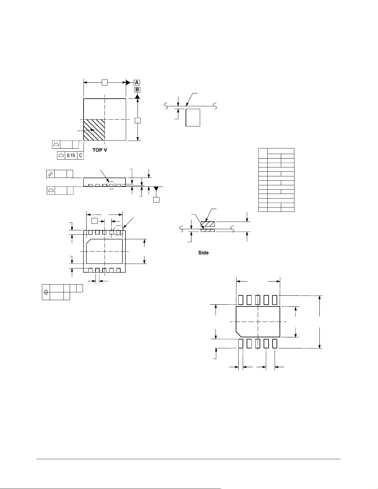
PACKAGE DIMENSIONS
DFN10, 3x3
MN SUFFIX
CASE 485C-01
ISSUE A
10X
REFERENCE
2X
2X
10X
10X
PIN 1
0.15 C
0.10 C
0.08 C
L
K
0.15
D
TOP VIEW
C
DETAIL B
SIDE VIEW
D2
e
15
(A3)
A
B
E
A1
DETAIL A
E2
NOTES:
1. DIMENSIONING AND TOLERANCING PER
EDGE OF PACKAGE
L1
DETAIL A
Bottom View
(Optional)
A
SEATING
PLANE
C
MOLD CMPD
EXPOSED Cu
ASME Y14.5M, 1994.
2. CONTROLLING DIMENSION: MILLIMETERS.
3. DIMENSION b APPLIES TO PLATED
TERMINAL AND IS MEASURED BETWEEN
0.25 AND 0.30 MM FROM TERMINAL.
4. COPLANARITY APPLIES TO THE EXPOSED
PAD AS WELL AS THE TERMINALS.
5. TERMINAL b MAY HAVE MOLD COMPOUND
MATERIAL ALONG SIDE EDGE. MOLD
FLASHING MAY NOT EXCEED 30 MICRONS
ONTO BOTTOM SURFACE OF TERMINAL b.
6. DETAILS A AND B SHOW OPTIONAL VIEWS
FOR END OF TERMINAL LEAD AT EDGE OF
PACKAGE.
MILLIMETERS
DIM MIN MAX
A 0.80 1.00
A1 0.00 0.05
A3 0.20 REF
b 0.18 0.30
D 3.00 BSC
D2 2.45 2.55
E 3.00 BSC
E2 1.75 1.85
e 0.50 BSC
K 0.19 TYP
L 0.35 0.45
L1 0.00 0.03
A3
A1
DETAIL B
Side View
(Optional)
0.10 C
0.05 C
10X
A B
NOTE 3
b
10 6
BOTTOM VIEW
SOLDERING FOOTPRINT*
2.6016
1.8508
0.5000 PITCH
DIMENSIONS: MILLIMETERS
10X
0.5651
2.1746
10X
0.3008
*For additional information on our Pb-Free strategy and soldering
details, please download the ON Semiconductor Soldering and
Mounting Techniques Reference Manual, SOLDERRM/D.
3.3048
http://onsemi.com
12

NCP5603
ON Semiconductor and are registered trademarks of Semiconductor Components Industries, LLC (SCILLC). SCILLC reserves the right to make changes without further notice
to any products herein. SCILLC makes no warranty, representation or guarantee regarding the suitability of its products for any particular purpose, nor does SCILLC assume any liability
arising out of the application or use of any product or circuit, and specifically disclaims any and all liability, including without limitation special, consequential or incidental damages.
“Typical” parameters which may be provided in SCILLC data sheets and/or specifications can and do vary in different applications and actual performance may vary over time. All
operating parameters, including “Typicals” must be validated for each customer application by customer's technical experts. SCILLC does not convey any license under its patent rights
nor the rights of others. SCILLC products are not designed, intended, or authorized for use as components in systems intended for surgical implant into the body, or other applications
intended to support or sustain life, or for any other application in which the failure of the SCILLC product could create a situation where personal injury or death may occur. Should
Buyer purchase or use SCILLC products for any such unintended or unauthorized application, Buyer shall indemnify and hold SCILLC and its officers, employees, subsidiaries, affiliates,
and distributors harmless against all claims, costs, damages, and expenses, and reasonable attorney fees arising out of, directly or indirectly, any claim of personal injury or death
associated with such unintended or unauthorized use, even if such claim alleges that SCILLC was negligent regarding the design or manufacture of the part. SCILLC is an Equal
Opportunity/Affirmative Action Employer. This literature is subject to all applicable copyright laws and is not for resale in any manner.
PUBLICATION ORDERING INFORMATION
LITERATURE FULFILLMENT:
Literature Distribution Center for ON Semiconductor
P.O. Box 5163, Denver, Colorado 80217 USA
Phone: 303-675-2175 or 800-344-3860 Toll Free USA/Canada
Fax: 303-675-2176 or 800-344-3867 Toll Free USA/Canada
Email: orderlit@onsemi.com
N. American Technical Support: 800-282-9855 Toll Free
USA/Canada
Europe, Middle East and Africa Technical Support:
Phone: 421 33 790 2910
Japan Customer Focus Center
Phone: 81-3-5773-3850
http://onsemi.com
ON Semiconductor Website: www.onsemi.com
Order Literature: http://www.onsemi.com/orderlit
For additional information, please contact your local
Sales Representative
NCP5603/D
13
 Loading...