

ON Semiconductor NCP5392P Datasheet

NCP5392P
2/3/4--Phase Controller for
CPU Applications
The NCP5392P provides up to a four--phase buck solution which
combines differential voltage sensing, differential phase current
sensing, and adaptive voltage positioning to provide accurately
regulated power for both Intel and AMD processors. Dual--edge
pulse--width modulation (PWM) combined with inductor current
sensing reduces system cost by providing the fastest initial response
to dynamic load events. Dual--edge multiphase modulation reduces
the total bul k and ceramic output capacitance required to meet
transient regulation specifications.
A high performance operational error amplifier is provided to
simplify compensation of the system. Dynamic Reference Injection
further simplifies loop compensation by eliminating the need to
compromise bet we en closed--loop transient response and Dynamic
VID performance.
In addition, NCP5392P provides an automatic power saving
feature (Auto--PSI). When Auto--PSI function is enabled, NCP5392P
will automatically detect the VID transitions and direct the Vcore
regulator in or out of low power states. As a result, the best efficiency
scheme is always chosen.
Features
Meets Intel’s VR11.1 Specifications
Meets AMD 6 Bit Code Specifications
Dual--edge PWM for Fastest Initial Response to Transient Loading
High Performance Operational Error Amplifier
Internal Soft Start
Dynamic Reference Injection
DAC Range from 0.375 V to 1.6 V
DAC Feed Forward Function
0.5% DAC Voltage Accurac y from 1.0 V to 1.6 V
True Differential Remote Voltage Sensing Amplifier
Phase--to--Phase Current Balancing
“Lossless” Differential Inductor Current Sensing
Differential Current Sense Amplifiers for each Phase
Adaptive Voltage Positioning (AVP)
Oscillator Frequency Range of 100 kHz – 1 MHz
Latched Over Voltage Protection (OVP)
Guaranteed Startup into Pre-- Charged Loads
Threshold Sensitive Enable Pin for VTT Sensing
Power Good Output with Internal Delays
Thermally Compensated Current Monitoring
Automatic Power Saving (AUTO PSI Mode)
Compatible to PSI Power Saving Requirements
This is a Pb--Free Device
Applications
Desktop Processors
http://onsemi.com
MARKING
DIAGRAM
1
401
40 PIN QFN, 6x6
MN SUFFIX
CASE 488AR
NCP5392P = Specific Device
Code
A = Assembly Location
WL = Wafer Lot
YY = Year
WW = Work Week
G = Pb-- Free Package
*Pin 41 is the thermal pad on the bottomof thedevice.
ORDERING INFORMATION
Device Package Shipping
NCP5392PMNR2G* QFN--40
(Pb--Free)
*Temperature Range: 0Cto85C
†For information on tape and reel specifications,
including part orientation and tape sizes, please
refer to our Tape and Reel Packaging Specification
Brochure, BRD8011/D.
NCP5392P
AWLYYWWG
†
2500/Tape & Reel
Semiconductor Components Industries, LLC, 2010
November, 2010 -- Rev. 2
1 Publication Order Number:
NCP5392P/D
NCP5392P
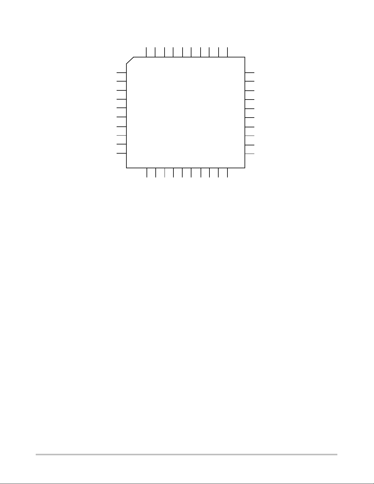
PIN CONNECTIONS
40
39
38
37
36
35
34G433G332G231
PSI
DAC
1
EN
2
VID0
3
VID1
4
VID2
5
VID3
6
VID4
7
VID5
8
VID6
9
VID7
10
ROSC
PH_PSI
VR_RDY
APSI_EN
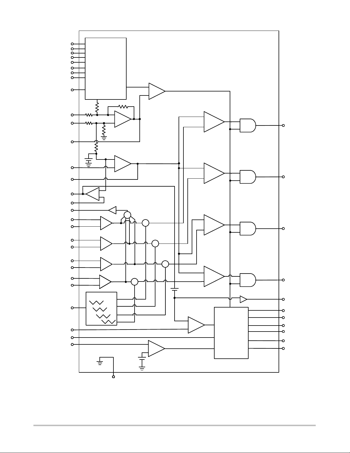
2/3/4--Phase Buck Controller
ILIM11IMON12VSP13VSN14DIFFOUT15COMP16VFB17VDRP18VDFB19CSSUM
VCC
12VMON
DRVON
NCP5392P
(QFN40)
20
Figure 1. NCP5392P QFN40 Pin Connections (Top View)
CS4
CS4N
CS3
CS3N
CS2
CS2N
CS1
CS1N
30
G1
29
28
27
26
25
24
23
22
21
http://onsemi.com
2
VID0
VID1
VID2
VID3
VID4
VID5
VID6
VID7/AMD
DAC
NCP5392P
Flexible DAC
Overvoltage
Protection
--
+
VSN
VSP
DIFFOUT
VFB
COMP
VDRP
VDFB
CSSUM
CS1P
CS1N
CS2P
CS2N
CS3P
CS3N
CS4P
CS4N
ROSC
ILIM
EN
VCC
+
1.3 V
+
--
+
--
+
--
+
--
+
--
Oscillator
--
+
Diff Amp
+
--
Droop Amp
-- 2 / 3
Gain = 6
Gain = 6
Gain = 6
Gain = 6
Error Amp
+
+
4.25 V
+
+
+
+
--
UVLO
+
--
+
--
+
--
+
+
+
--
+
-ILimit
Control,
Fault Logic
and
Monitor
Circuits
G1
G2
G3
G4
IMON
DRVON
PSI
APSI_EN
PH_PSI
12VMON
VR_RDY
GND (FLAG)
Figure 2. NCP5392P Block Diagram
http://onsemi.com
3
NCP5392P
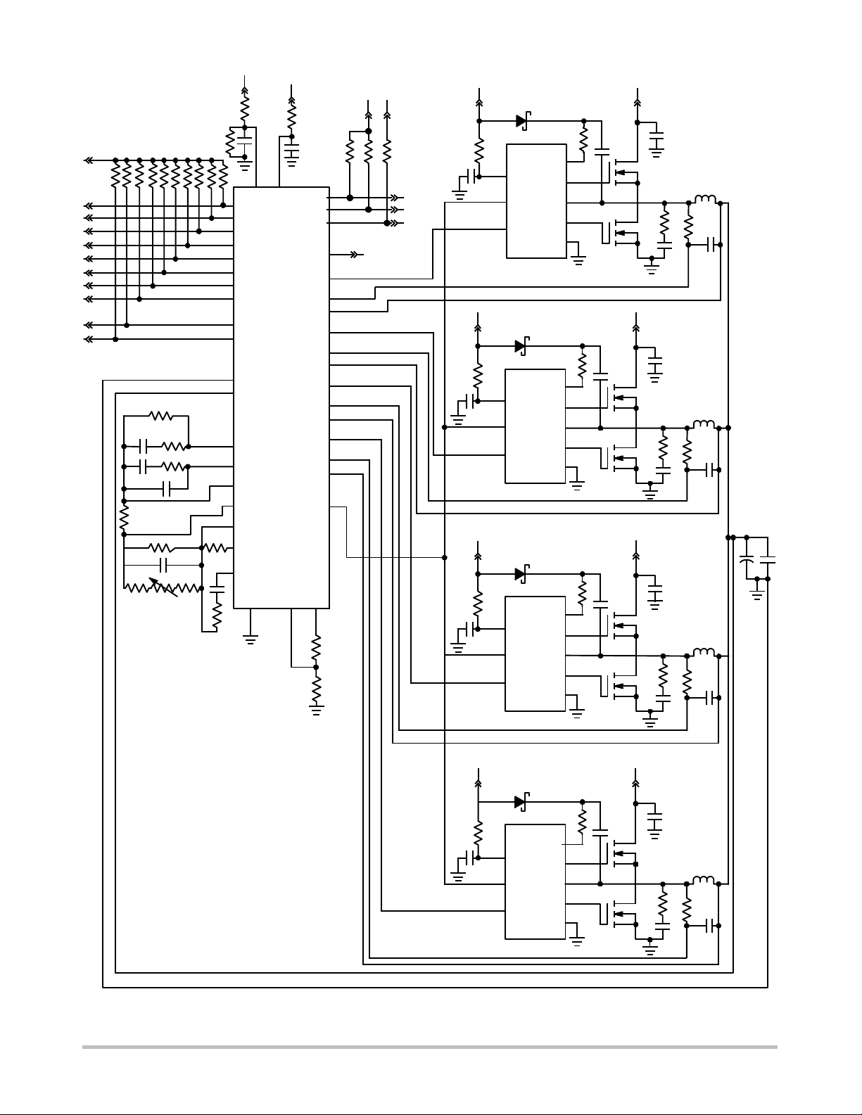
VTT
RFB
CFB1
CF
RDRP
RISO1 RISO2RT2
RFB1
RF
CH
RNOR
CDFB
12V_FILTER
2
3
4
5
6
7
8
9
1
39
14
13
15
16
17
18
19
R6R6
20
36
CDNI
RDNP
+5V
3534
VID0
VID1
VID2
VID3
VID4
VID5
VID6
VID7
EN
VR_RDY
VSN
VSP
DIFFOUT
COMP
VFB
VDRP
VDFB
CSSUM
DAC
41 11 10
12VMON
NCP5392P
GND
VCC
APSI_EN
ILIM
PH_PSI
IMON
CS1P
CS1N
CS2P
CS2N
CS3P
CS3N
CS4P
CS4N
DRVON
G1
G2
G3
G4
ROSC
37
38
40
12
30
22
21
31
24
23
32
26
25
33
28
27
29
RLIM1
RLIM2
VTTU2+5V
IMON
PSIPSI
APSI_EN
PH_PSI
12V_FILTER12V_FILTER
D1
C4
C3
C1
VCC
NCP5359
OD
IN
VCC
NCP5359
OD
IN
VCC
NCP5359
OD
IN
BST
DRH
SW
DRL
PGND
BST
DRH
SW
DRL
PGND
BST
DRH
SW
DRL
PGND
12V_FILTER12V_FILTER
12V_FILTER12V_FILTER
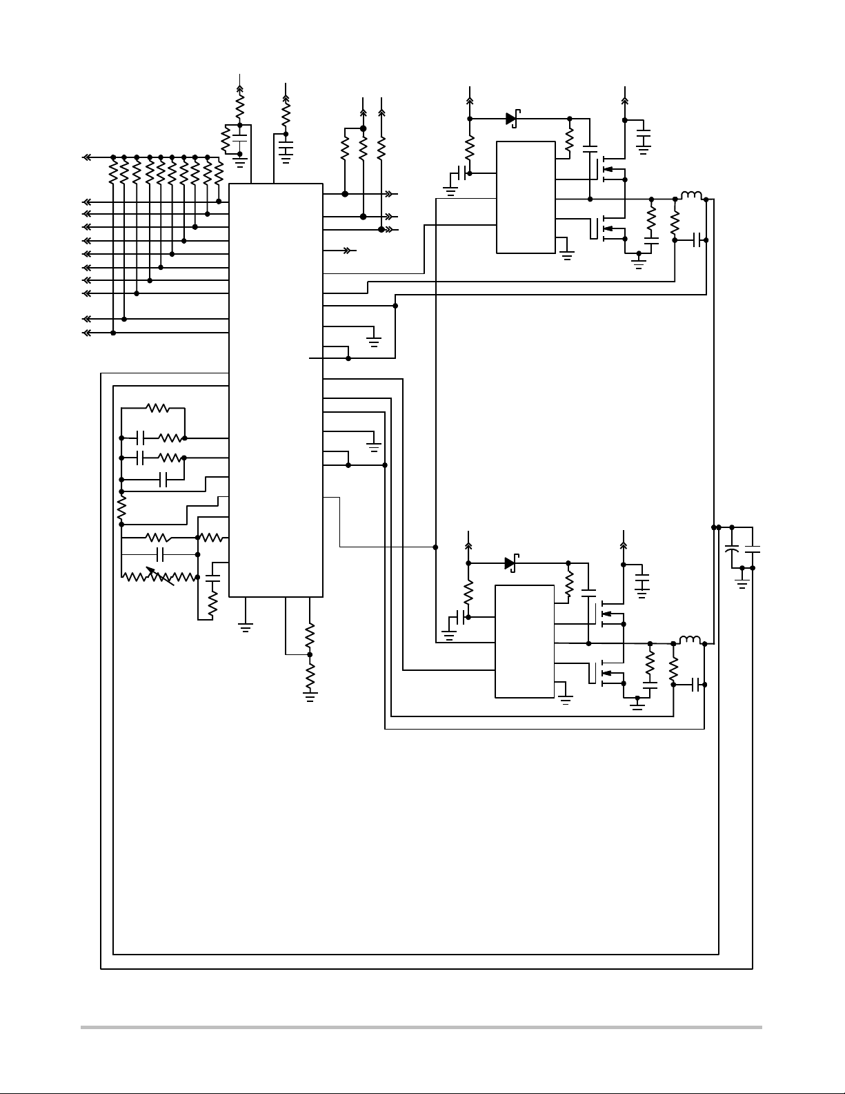
Q1
Q2 R2 RS1
C2
L1
CS1
+
CPU GND
VCCP
VSSN
BST
VCC
DRH
NCP5359
SW
OD
DRL
IN
PGND
Figure 3. Application Schematic for Four Phases
http://onsemi.com
4
12V_FILTER12V_FILTER
NCP5392P
VTT
RFB
CFB1
CF
RDRP
RISO1 RISO2RT2
RFB1
RF
CH
RNOR
CDFB
12V_FILTER
2
3
4
5
6
7
8
9
1
39
14
13
15
16
17
18
19
R6R6
20
36
CDNI
RDNP
+5V
3534
VID0
VID1
VID2
VID3
VID4
VID5
VID6
VID7
EN
VR_RDY
VSN
VSP
DIFFOUT
COMP
VFB
VDRP
VDFB
CSSUM
DAC
41 11 10
12VMON
NCP5392
GND
VCC
APSI_EN
ILIM
PH_PSI
IMON
CS1P
CS1N
CS2P
CS2N
CS3P
CS3N
CS4P
CS4N
DRVON
G1
G2
G3
G4
ROSC
37
38
40
12
30
22
21
31
24
23
32
26
25
33
28
27
29
RLIM1
RLIM2
VTTU2+5V
IMON
PSIPSI
APSI_EN
PH_PSI
12V_FILTER12V_FILTER
D1
C4
C3
C1
VCC
NCP5359
OD
IN
VCC
NCP5359
OD
IN
VCC
NCP5359
OD
IN
BST
DRH
SW
DRL
PGND
BST
DRH
SW
DRL
PGND
BST
DRH
SW
DRL
PGND
Q1
L1
Q2
12V_FILTER12V_FILTER
12V_FILTER12V_FILTER
RS1R2
C2
CS1
+
CPU GND
VCCP
VSSN
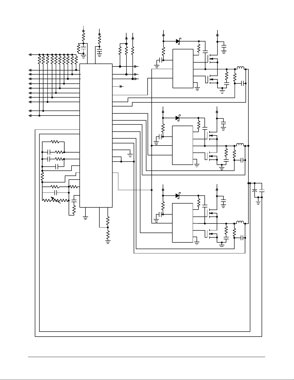
Figure 4. Application Schematic for Three Phases
http://onsemi.com
5
NCP5392P
VTT
RFB
CFB1
CF
RDRP
RISO1 RISO2RT2
RFB1
RF
CH
RNOR
CDFB
12V_FILTER
2
3
4
5
6
7
8
9
1
39
14
13
15
16
17
18
19
R6R6
20
36
CDNI
RDNP
+5V
3534
VID0
VID1
VID2
VID3
VID4
VID5
VID6
VID7
EN
VR_RDY
VSN
VSP
DIFFOUT
COMP
VFB
VDRP
VDFB
CSSUM
DAC
41 11 10
12VMON
NCP5392
GND
VCC
APSI_EN
ILIM
PH_PSI
IMON
CS1P
CS1N
CS2P
CS2N
CS3P
CS3N
CS4P
CS4N
DRVON
G1
G2
G3
G4
ROSC
37
38
40
12
30
22
21
31
24
23
32
26
25
33
28
27
29
RLIM1
RLIM2
VTTU2+5V
IMON
RNTC1
PSIPSI
APSI_EN
PH_PSI
12V_FILTER12V_FILTER
D1
C4
C3
C1
VCC
NCP5359
OD
IN
VCC
NCP5359
OD
IN
BST
DRH
SW
DRL
PGND
BST
DRH
SW
DRL
PGND
Q1
L1
Q2
12V_FILTER12V_FILTER
RS1R2
C2
CS1
+
CPU GND
VCCP
VSSN
Figure 5. Application Schematic for Two Phases
http://onsemi.com
6

NCP5392P
PIN DESCRIPTIONS
Pin No. Symbol Description
1 EN Threshold sensitive input. High = startup, Low = shutdown.
2 VID0 Voltage ID DAC input
3 VID1 Voltage ID DAC input
4 VID2 Voltage ID DAC input
5 VID3 Voltage ID DAC input
6 VID4 Voltage ID DAC input
7 VID5 Voltage ID DAC input
8 VID6 Voltage ID DAC input
9 VID7/AMD Voltage ID DAC input. Pull to VCC(5 V) to enable AMD 6--bit DAC code.
10 ROSC A resistance from this pin to ground programs the oscillator frequency according to fSW. This pin supplies a
11 ILIM Overcurrent shutdown threshold setting. Connect this pin to the ROSC pin via a resistor divider as shown in
12 IMON 0 mV to 900 mV analog signal proportional to the output load current. VSN referenced
13 VSP Non--inverting input to the internal differential remote sense amplifier
14 VSN Inverting input to the internal differential remote sense amplifier
15 DIFFOUT Output of the differential remote sense amplifier
16 COMP Output of the error amplifier
17 VFB Compensation Amplifier Voltage feedback
18 VDRP Voltage output signal proportional to current used for current limit and output voltage droop
19 VDFB Droop Amplifier Voltage Feedback
20 CSSUM Inverted Sum of the Differential Current Sense inputs. Av=CSSUM/CSx = --4
21 CS1N Inverting input to current sense amplifier #1
22 CS1 Non-- inverting input to current sense amplifier #1
23 CS2N Inverting input to current sense amplifier #2
24 CS2 Non-- inverting input to current sense amplifier #2
25 CS3N Inverting input to current sense amplifier #3
26 CS3 Non-- inverting input to current sense amplifier #3
27 CS4N Inverting input to current sense amplifier #4
28 CS4 Non-- inverting input to current sense amplifier #4
29 DRVON Bidirectional Gate Drive Enable
30 G1 PWM output pulse to gate driver. 3-- level output: Low = LSFET Enabled, Mid = Diode Emulation Enabled,
31 G2 PWM output pulse to gate driver. 3-- level output (see G1)
32 G3 PWM output pulse to gate driver. 3-- level output (see G1)
33 G4 PWM output pulse to gate driver. 3-- level output (see G1)
34 12VMON Monitor a 12 V input through a resistor divider.
35 VCC Power for the internal control circuits.
36 DAC DAC Feed Forward Output
37 PSI Power Saving Control. Low = power saving operation, High = normal operation. PSI signal has higher priority
38 APSI_EN APSI_EN High: Enable AUTO PSI function. When PSI = low, system will be forced into PSI mode, uncondi-
39 VR_RDY Open collector output. High indicates that the output is regulating
40 PH_PSI PH_PSI Pin select one or two phase operation in PSI mode. PH_PSI = low, two phase operation, PH_PSI =
FLAG GND Power supply return (QFN Flag)
trimmed output voltage of 2 V.
the Application Schematics. To disable the overcurrent feature, connect this pin directly to the ROSC pin. T o
guarantee correct operation, this pin should only be connected to the voltage generated by the ROSC pin; do
not connect this pin to any externally generated voltages.
High = HSFET Enabled
over APSI_EN signal.
tionally. When PSI = high, APSI_EN will determine if the system needs to be in AUTO PSI mode. Once in
AUTO PSI mode, system switches on/off PSI functions automatically based on VID change status.
high, one phase operation.
http://onsemi.com
7
NCP5392P
PIN CONNECTIONS VS. PHASE COUNT
Number of Phases G4 G3 G2 G1 CS4--CS4N CS3--CS3N CS2--CS2N CS1--CS1N
4 Phase 4
Out
3 Tie to
GND
2 Tie to
GND
MAXIMUM RATINGS
ELECTRICAL INFORMATION
Pin Symbol
COMP 5.5 V -- 0 . 3 V 10 mA 10 mA
V
DRP
V– GND + 300 mV GND – 300 mV 1mA 1mA
DIFFOUT 5.5 V -- 0 . 3 V 20 mA 20 mA
VR_RDY 5.5 V -- 0 . 3 V N/A 20 mA
VCC 7.0 V -- 0 . 3 V N/A 10 mA
ROSC 5.5 V -- 0 . 3 V 1mA N/A
IMON Output 1.1 V
All Other Pins 5.5 V -- 0 . 3 V
*All signals referenced to AGND unless otherwise noted.
Phase 3
Out
Phase 3
Out
Phase 2
Out
Phase 2
Out
Phase 2
Out
Tie to
GND
V
MAX
Phase 1
Out
Phase 1
Out
Phase 1
Out
Phase 4 CS
input
TietoCSN
pin used
TietoCSN
pin used
V
MIN
Phase 3 CS
input
Phase 3 CS
input
Phase 2 CS
input
I
SOURCE
Phase 2 CS
input
Phase 2 CS
input
TietoCSN
pin used
Phase 1 CS
Phase 1 CS
Phase 1 CS
I
SINK
5.5 V -- 0 . 3 V 5mA 5mA
input
input
input
THERMAL INFORMATION
Rating
Thermal Characteristic, QFN Package (Note 1) R
Operating Junction Temperature Range (Note 2) T
Operating Ambient Temperature Range T
Maximum Storage T emperature Range T
Symbol Value Unit
θ
JA
J
A
STG
34 C/W
0to125 C
0to+85 C
--55 to +150 C
Moisture Sensitivity Level, QFN Package MSL 1
Stresses exceeding Maximum Ratings may damage the device. Maximum Ratings are stress ratings only. Functional operation above the
Recommended Operating Conditions is not implied. Extended exposure to stresses above the Recommended Operating Conditions may affect
device reliability.
*The maximum package power dissipation must be observed.
1. JESD 51--5 (1S2P Direct-- Attach Method) with 0 LFM.
2. JESD 51--7 (1S2P Direct-- Attach Method) with 0 LFM.
http://onsemi.com
8
NCP5392P
ELECTRICAL CHARACTERISTICS
(Unless otherwise stated: 0C<TA<85C; 4.75 V < VCC< 5.25 V; All DAC Codes; C
Parameter
Test Conditions Min Typ Max Unit
ERROR AMPLIFIER
Input Bias Current (Note 3)
Noninverting Voltage Range (Note 3) 0 1.3 3 V
Input Offset Voltage (Note 3) V+=V-- =1.1V -- 1 . 0 -- 1.0 mV
Open Loop DC Gain CL=60pFtoGND,
R
=10KΩ to GND
L
Open Loop Unity Gain Bandwidth CL=60pFtoGND,
R
=10KΩ to GND
L
Open Loop Phase Margin CL=60pFtoGND,
R
=10KΩ to GND
L
Slew Rate ΔVin= 100 mV, G = -- 10 V/V,
ΔV
=1.5V–2.5V,
out
C
=60pFtoGND,
L
DC Load = 125 mAtoGND
Maximum Output Voltage I
Minimum Output Voltage I
Output source current (Note 3) V
Output sink current (Note 3) V
=2.0mA 3.5 -- -- V
SOURCE
=0.2mA -- -- 50 mV
SINK
=3.5V 2 -- -- mA
out
=1.0V 2 -- -- mA
out
DIFFERENTIAL SUMMING AMPLIFIER
VSN Input Bias Current
VSN Voltage = 0 V 30 mA
VSP Input Resistance DRVON = Low
DRVON = High
VSP Input Bias Voltage DRVON = Low
DRVON = High
Input Voltage Range (Note 3) -- 0 . 3 -- 3.0 V
--3 dB Bandwidth CL=80pFtoGND,
R
=10KΩ to GND
L
Closed Loop DC Gain VS to Diffout VS+ to VS-- = 0.5 to 1.6 V 0.98 1.0 1.025 V/V
Maximum Output Voltage I
Minimum Output Voltage I
Output source current (Note 3) V
Output sink current (Note 3) V
=2mA 3.0 -- -- V
SOURCE
=2mA -- -- 0.5 V
SINK
=3V 2.0 -- -- mA
out
=0.5V 2.0 -- -- mA
out
INTERNAL OFFSET VOLTAGE
Offset Voltage to the (+) Pin of the
Error Amp and the VDRP pin
VDROOP AMPLIFIER
Input Bias Current (Note 3)
Non--inverting Voltage Range (Note 3) 0 1.3 3 V
Input Offset Voltage (Note 3) V+=V-- =1.1V -- 4 . 0 -- 4.0 mV
Open Loop DC Gain CL= 20 pF to GND including
ESD, R
=1kΩ to GND
L
Open Loop Unity Gain Bandwidth CL= 20 pF to GND including
ESD, R
=1kΩ to GND
L
Slew Rate CL= 20 pF to GND including
ESD, R
Maximum Output Voltage I
Minimum Output Voltage I
Output source current (Note 3) V
Output sink current (Note 3) V
=1kΩ to GND
L
=4.0mA 3 -- -- V
SOURCE
=1.0mA -- -- 1 V
SINK
=3.0V 4 -- -- mA
out
=1.0V 1 -- -- mA
out
3. Guaranteed by design, not tested in production.
=0.1mF)
VCC
--200 200 nA
-- 100 dB
-- 10 -- MHz
-- 80 --
-- 5 -- V/ms
1.5
kΩ
17
0.09
0.66
-- 10 -- MHz
-- 1.30 -- V
--200 200 nA
-- 100 dB
-- 10 -- MHz
-- 5 -- V/ms
V
http://onsemi.com
9
NCP5392P
ELECTRICAL CHARACTERISTICS
(Unless otherwise stated: 0C<TA<85C; 4.75 V < VCC< 5.25 V; All DAC Codes; C
Parameter UnitMaxTypMinTest Conditions
CSSUM AMPLIFIER
Current Sense Input to CSSUM Gain
Current Sense Input to CSSUM --3 dB
Bandwidth
Current Sense Input to CSSUM
Output Slew Rate
Current Summing Amp Output Offset
--60 mV < CS < 60 mV -- 4.00 --3.88 --3.76 V/V
CL=10pFtoGND,
R
=10kΩ to GND
L
ΔVin=25mV,CL=10pFto
GND, Load = 1 k to 1.3 V
CSx – CSNx = 0, CSx = 1.1 V -- 1 5 -- +15 mV
Voltage
Maximum CSSUM Output Voltage CSx – CSxN = --0.15 V
(All Phases) I
SOURCE
=1mA
Minimum CSSUM Output Voltage CSx – CSxN = 0.066 V
Output source current (Note 3) V
Output sink current (Note 3) V
(All Phases) I
=3.0V 1 -- -- mA
out
=0.3V 1 -- -- mA
out
SINK
=1mA
PSI (Power Saving Control, Active Low)
Enable High Input Leakage Current
Upper Threshold V
Lower Threshold V
Hysteresis V
External1KPullupto3.3V -- -- 1.0 mA
UPPER
LOWER
-- V
UPPER
LOWER
APSI_EN (AUTO PSI Function Enable, Active High)
Enable High Input Leakage Current
Upper Threshold V
Lower Threshold V
Hysteresis V
External 1k Pullup to 3.3 V -- -- 1.0 mA
UPPER
LOWER
-- V
UPPER
LOWER
PH_PSI (PSI Phase Selection)
Enable High Input Leakage Current
Upper Threshold V
Lower Threshold V
External 1k Pullup to 3.3 V -- -- 1.0 mA
UPPER
LOWER
DRVON
Output High Voltage
Sourcing 500 mA 3.0 -- -- V
Sourcing Current for Output High VCC=5V -- 2.5 4.0 mA
Output Low Voltage Sinking 500 mA -- -- 0.7 V
Sinking Current for Output Low 2.5 -- -- mA
Delay Time Propagation Delay from EN Low
to DRVON
Rise Time CL(PCB) = 20 pF, ΔVo= 10% to
90%
Fall Time CL(PCB) = 20 pF, ΔVo= 10% to
90%
Internal Pulldown Resistance 35 70 140 kΩ
VCCVoltage when DRVON
Output Valid
CURRENT SENSE AMPLIFIERS
Input Bias Current (Note 3)
CSx = CSxN = 1.4 V -- 0 -- nA
Common Mode Input Voltage Range
(Note 3)
Differential Mode Input Voltage Range
(Note 3)
3. Guaranteed by design, not tested in production.
=0.1mF)
VCC
-- 4 -- MHz
-- 4 -- V/s
3.0 -- -- V
-- -- 0.3 V
-- 650 770 mV
450 550 -- mV
-- 100 -- mV
-- 650 770 mV
450 550 -- mV
-- 100 -- mV
-- -- 0.7 V
0.3 -- -- V
-- 10 -- ns
-- 130 -- ns
-- 10 -- ns
-- -- 2.0 V
-- 0 . 3 -- 2.0 V
--120 -- 120 mV
CC
CC
http://onsemi.com
10
 Loading...