

Page 1
High and Low Side Gate
Driver, High Performance,
700 V, with 3.5 A Source
and 3 A Sink Currents
NCP51530
NCP51530 is a 700 V high side and low side driver with 3.5 A
source & 3 A sink current drive capability for AC−DC power supplies
and inverters. NCP51530 offers best in class propagation delay, low
quiescent current and low switching current at high frequencies of
operation. This device is tailored for highly efficient power supplies
operating at high frequencies. NCP51530 is offered in two versions,
NCP51530A/B. NCP51530A has a typical 60 ns propagation delay,
while NCP51530B has a typical propagation delay of 25 ns.
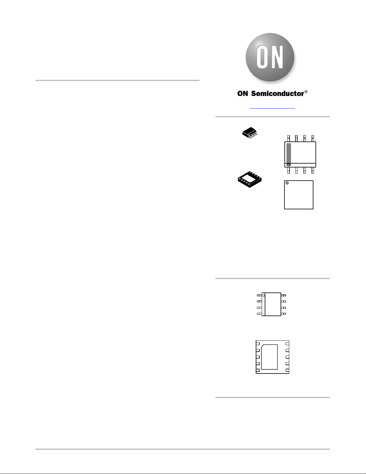
NCP51530 comes in SOIC8 and DFN10 packages.
Features
• High voltage range: Up to 700 V
• NCP51530A: Typical 60 ns Propagation Delay
• NCP51530B: Typical 25 ns Propagation Delay
• Low Quiescent and Operating Currents
• 15 ns Max Rise and Fall Time
• 3.5 A Source / 3 A Sink Currents
• Under−voltage Lockout for Both Channels
• 3.3 V and 5 V Input Logic Compatible
• High dv/dt Immunity up to 50 V/ns
• Pin to Pin Compatible with Industry Standard Half−bridge ICs.
• Matched Propagation Delay (7 ns Max)
• High Negative Transient Immunity on Bridge Pin
• DFN10 Package Offers Both Improved Creepage and Exposed Pad
Applications
• High−density SMPS for Servers, Telecom and Industrial
• Half/Full−bridge & LLC Converters
• Active Clamp Flyback/Forward Converters
• Solar Inverters & Motor Controls
• Electric Power Steering
www.onsemi.com
MARKING
DIAGRAMS
1
SOIC−8
D SUFFIX
CASE 751−07
1
DFN10
MN SUFFIX
CASE 506DJ
NCP51530 = Specific Device Code
x = A or B version
A = Assembly Location
WL = Wafer Lot
YY = Year
WW = Work Week
G = Pb−Free Package
(Note: Microdot may be in either location)
PINOUT INFORMATION
HIN
LIN
GND
LO
8 Pin Package
(Top View)
VCC
GND
GND
1
HIN
LIN
10 Pin DFN Package
(Top View)
8
NCP51530x
ALYW
G
1
51530x
ALYWG
G
1
VB
HO
HB
VCC
VB
HO
HB
NC
LO
© Semiconductor Components Industries, LLC, 2018
September, 2020 − Rev. 4
ORDERING INFORMATION
See detailed ordering and shipping information on page 22 of
this data sheet.
1 Publication Order Number:
NCP51530/D
Page 2
NCP51530
HIN
LIN
GND
LO
SOIC8 DFN10
(Top View) (Top View)
VB
HO
HB
VCC
VCC
HIN
LIN
GND
GND
Table 1. PIN DESCRIPTION SOIC 8 PACKAGE
Pin Out Name Function
1 HIN High side input
2 LIN Low side input
3 GND Ground reference
4 LO Low side output
5 VCC Low side and logic supply
6 HB High side supply return
7 HO High side output
8 VB High side voltage supply
VB
HO
HB
NC
LO
Table 2. PIN DESCRIPTION DFN10 PACKAGE
Pin Out Name Function
1 VCC Low side and logic supply
2 HIN High side input
3 LIN Low side input
4 GND Ground reference
5 GND Ground reference
6 LO Low side output
7 NC No Connect
8 HB High side supply return
9 HO High side output
10 VB High side voltage supply
www.onsemi.com
2
Page 3
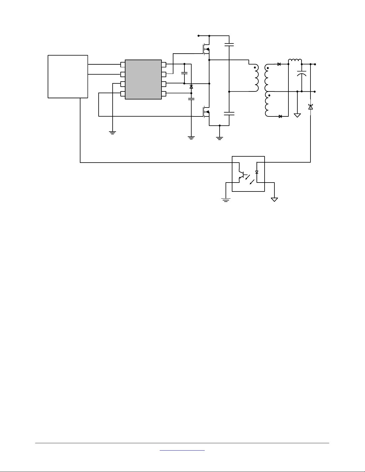
NCP51530
VHV
ADRV
PWM CONTROLLER
LDRV
COMP
Figure 1. Simplified Applications Schematic for a Half−Bridge Converter (SOIC8)
HIN
LIN
GND
LO
NCP51530
VB
HO
HB
VCC
www.onsemi.com
3
Page 4
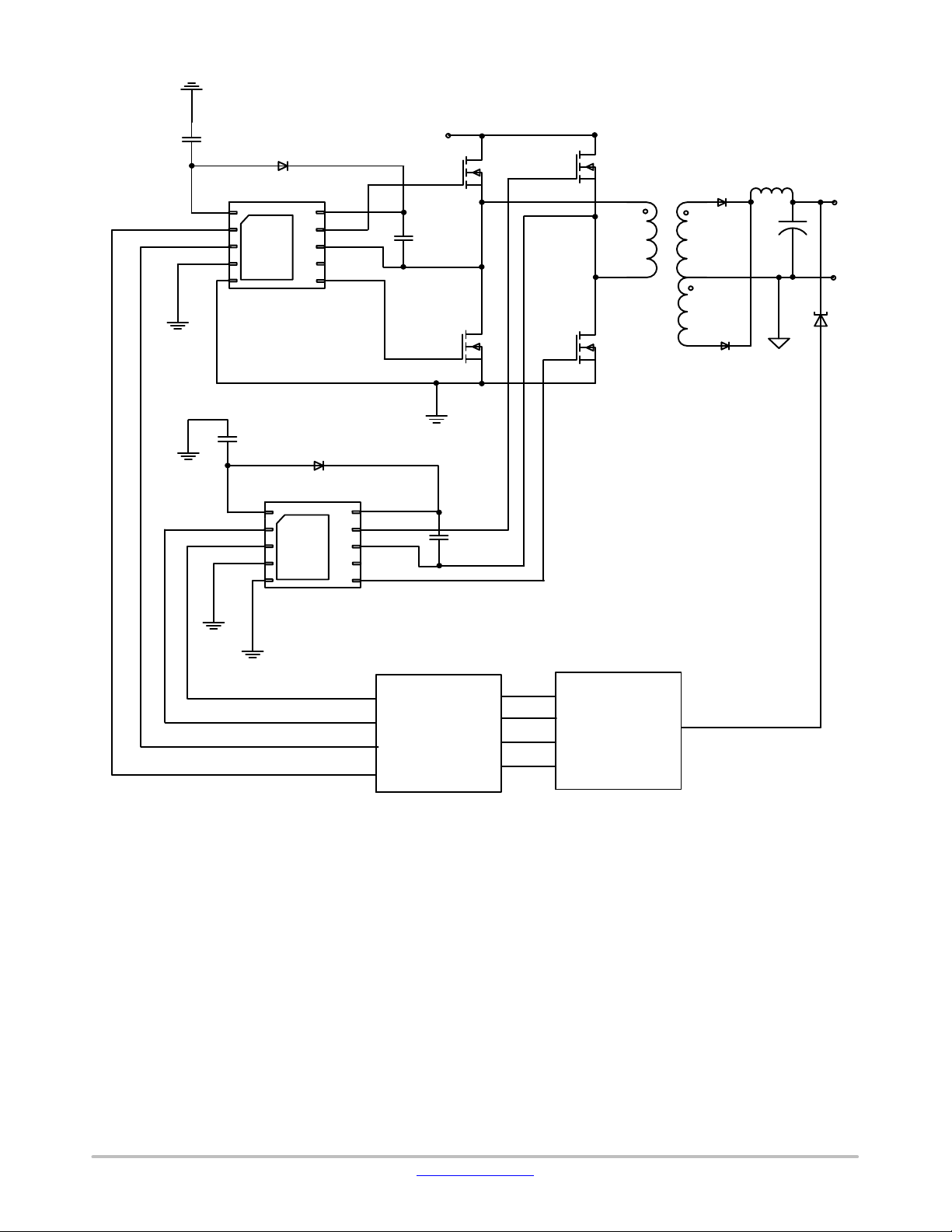
NCP51530
VHV
VCC
HIN
LIN
GND
GND
VCC
HIN
LIN
GND
GND
VB
HO
HB
NC
LO
VB
HO
HB
NC
LO
LIN 1
HIN 1
LIN 2
HIN 2
Digital Isolator
Micro Controller
Figure 2. Simplified Applications Schematic for a Full Bridge Converter (DFN 10)
www.onsemi.com
4
Page 5
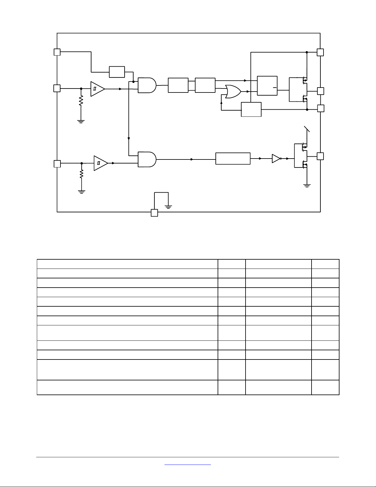
NCP51530
VCC
HIN
LIN
VB
UV
Detect
Q
UV
DETECT
S
Q
R
VCC
HO
HB
LO
Pulse
Trigg er
r
r
GND
Level
Shifter
DELAY
Figure 3. Internal Block Diagram for NCP51530
Table 3. ABSOLUTE MAXIMUM RATINGS All voltages are referenced to GND pin.
Rating Symbol Value Unit
Input voltage range V
High side boot pin voltage V
High side floating voltage VB−V
High side drive output voltage V
Low side drive output voltage V
CC
B
HB
HO
LO
Allowable hb slew rate dVHB/dt 50 V/ns
Drive input voltage V
Junction temperature T
Storage temperature range T
LIN
V
HIN
J(MAX)
STG
,
ESD Capability (Note 1)
Human Body Model per JEDEC Standard JESD22−A114E.
Charge Device Model per JEDEC Standard JESD22−C101E.
Lead Temperature Soldering
Reflow (SMD Styles ONLY), Pb−Free Versions (Note 2)
Stresses exceeding those listed in the Maximum Ratings table may damage the device. If any of these limits are exceeded, device functionality
should not be assumed, damage may occur and reliability may be affected.
1. This device series incorporates ESD protection and is tested by the following methods. ESD Human Body Model tested per
AEC−Q100−002(EIA/JESD22−A114)
ESD Charged Device Model tested per AEC−Q100−11(EIA/JESD22−C101E)
Latchup Current Maximum Rating: ≤150 mA per JEDEC standard: JESD78
2. For information, please refer to our Soldering and Mounting Techniques Reference Manual, SOLDERRM/D
−0.3 to 20 V
−0.3 to 720 V
−0.3 to 20 V
VHB – 0.3 to VB + 0.3
−0.3 to V
+ 0.3 V
CC
−5 to VCC + 0.3 V
150° C
−55° to 150° C
4000
1000
260 °C
V
V
www.onsemi.com
5
Page 6
NCP51530
t
Table 4. THERMAL CHARACTERSTICS
Rating Symbol Value Unit
Thermal Characteristics, SOIC8 (Note 3)
Thermal Resistance, Junction to Air
Thermal Characteristics, DFN10
Thermal Resistance, Junction to Air (Note 4)
3. Refer to ELECTRICAL CHARACTERSTICS and APPLICATION INFORMATION for Safe Operating Area.
4. Values based on copper area of 50 mm
2
of 1 oz thickness and FR4 PCB substrate.
R
q
JA
R
q
JA
Table 5. RECOMMENDED OPERATING CONDITIONS
Rating Symbol Min Max Unit
Input Voltage Range V
High Side Floating Voltage VB−V
High Side Bridge pin Voltage V
High Side Output Voltage V
High Side Output Voltage V
Input Voltage on LIN and HIN pins V
LIN
V
HIN
Operating Junction Temperature Range T
CC
HB
HB
HO
LO
,
J
10 17 V
10 17 V
−1 700 V
V
GND V
GND VCC−2 V
−40 125 °C
183 °C/W
162 °C/W
HB
V
B
CC
V
V
Table 6. ELECTRICAL CHARACTERISTICS
(−40°C <T
< 125°C, V
J
Typical values are at T
Parameters
SUPPLY SECTION
quiescent current V
V
CC
VCC operating current f = 500 kHz, C
Boot voltage quiescent current V
Boot voltage operating current f = 500 kHz, C
HB to GND quiescent current VHS = VHB = 700 V I
INPUT SECTION
Input rising threshold
Input falling threshold V
Input voltage Hysteresis V
Input pulldown resistance V
UNDER VOLTAGE LOCKOUT (UVLO)
ON VCC Rising V
V
CC
VCC hysteresis V
VB ON VB Rising V
VB hysteresis V
High Side Startup Time Time between VB > UVLO & 1
LO GATE DRIVER
Low level output voltage
High level output voltage ILO = −100 mA, V
Peak source current VLO = 0 V I
=V
CC
= 25°C.)
J
=12V, V
B
= GND, outputs are not loaded, all voltages are referenced to GND; unless otherwise noted,
HB
Test Conditions Symbol Min Typ Max Unit
LIN=VHIN
LIN
=0 I
= 0 I
LOAD
= V
= 0 V I
HIN
= 0 I
LOAD
V
= 5 V R
XIN
s
HO Pulse
ILO = 100 mA V
= V
LOH
−V
LO
CC
CCQ
CCO
BQ
BO
HBQ
HIT
LIT
IHYS
IN
CCon
CChys
Bon
Bhyst
T
startup
LOL
V
LOH
LOpullup
0.15 0.25 mA
0.7 1.0 mA
0.1 0.15 mA
0.7 1.0 mA
6 11
2.3 2.7 3.1 V
1 1.4 1.8 V
1.3 V
100 175 250
8.6 9.1 9.6 V
0.5 V
8 8.5 9 V
0.5 V
10
0.125 V
0.150 V
3.5 A
mA
kW
ms
www.onsemi.com
6
Page 7
NCP51530
Table 6. ELECTRICAL CHARACTERISTICS
(−40°C <T
< 125°C, V
J
Typical values are at T
Parameters UnitMaxTypMinSymbolTest Conditions
LO GATE DRIVER
Peak sink current
HO GATE DRIVER
Low level output voltage
High level output voltage IHO = −100 mA, V
Peak source current VHO = 0 V I
Peak sink current VHO = 12 V I
OUTPUT RISE AND FALL TIME
Rise Time LO, HO
Fall Time LO, HO C
DELAY MATCHING
LI ON, HI OFF
LI OFF, HI ON
TIMING
Minimum Input Filter (NCP51530A)
PROPAGATION DELAY
NCP51530A
V
falling to VLO falling C
LI
VHI falling to VHO falling C
VLI rising to VLO rising C
VHI rising to VHO rising C
PROPAGATION DELAY
NCP51530B
V
falling to VLO falling C
LI
VHI falling to VHO falling C
VLI rising to VLO rising C
VHI rising to VHO rising C
=V
CC
= 25°C.)
J
=12V, V
B
= GND, outputs are not loaded, all voltages are referenced to GND; unless otherwise noted,
HB
VLO = 12 V I
IHO = 100 mA V
= V
HOH
–V
HO
C
= 1000 pF T
load
= 1000 pF T
load
HB
Pulse width = 1 ms
Pulse width = 1 ms
V
= 5 V , Input pulse width
XIN
above which output change occurs.
= 0, Minimum On/Off−time
load
to register as a valid change =
50 ns
= 0, Minimum On/Off−time
load
to register as a valid change =
50 ns
= 0, Minimum On/Off−time
load
to register as a valid change =
50 ns
= 0, Minimum On/Off−time
load
to register as a valid change =
50 ns
= 0, Minimum On/Off−time
load
to register as a valid change =
50 ns
= 0, Minimum On/Off−time
load
to register as a valid change =
50 ns
= 0, Minimum On/Off−time
load
to register as a valid change =
50 ns
= 0, Minimum On/Off−time
load
to register as a valid change =
50 ns
LOpulldown
HOL
V
HOH
HOpullup
HOpulldown
R
F
T
MON
T
MOFF
T
FT
T
DLFF
T
DHFF
T
DLRR
T
DHRR
T
DLFF
T
DHFF
T
DLRR
T
DHRR
3.0 A
0.125 V
0.150 V
3.5 A
3.0 A
8 15 ns
8 15 ns
7 ns
7 ns
30 40 ns
60 100 ns
60 100 ns
60 100 ns
60 100 ns
25 40 ns
25 40 ns
25 40 ns
25 40 ns
www.onsemi.com
7
Page 8
NCP51530
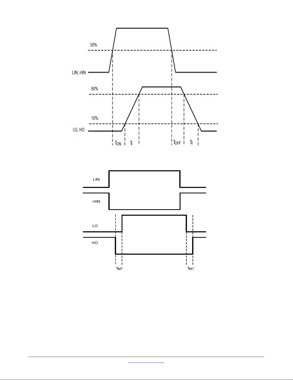
Figure 4. Propagation Delay, Rise and Fall Times
Figure 5. Delay Matching
www.onsemi.com
8
Page 9

NCP51530
Figure 6. NCP51530 Operating Currents (No Load, V
CC
= 12V)
Figure 7. NCP51530 Operating Currents (1nF load, VCC = 12V)
www.onsemi.com
9
Page 10

NCP51530
9.7
9.6
9.5
9.4
9.3
9.2
9.1
ON (V)
CC
9
V
8.9
8.8
8.7
8.6
8.5
−40.0 −20.0 0.0 20.0 40.0 60.0 80.0 100.0 120.0 140.0
TEMPERATURE (°C)
Figure 8. VCCON vs Temperature
1
0.9
0.8
0.7
0.6
0.5
ON (V)
Hyst
0.4
V
0.3
0.2
0.1
0
−40.0 −20.0 0.0 20.0 40.0 60.0 80.0 100.0 120.0 140.0
TEMPERATURE (°C)
Figure 10. VCCHyst vs Temperature
9.2
9.1
9
8.9
8.8
8.7
8.6
8.5
OFF (V)
8.4
CC
V
8.3
8.2
8.1
8
7.9
7.8
−40.0 −20.0 0.0 20.0 40.0 60.0 80.0 100.0 120.0 140.0
TEMPERATURE (°C)
Figure 9. VCCOFF vs Temperature
9.2
9.1
9
8.9
8.8
8.7
8.6
ON (V)
B
8.5
V
8.4
8.3
8.2
8.1
8
−40.0 −20.0 0.0 20.0 40.0 60.0 80.0 100.0 120.0 140.0
TEMPERATURE (°C)
Figure 11. VBON vs Temperature
8.8
8.7
8.6
8.5
8.4
8.3
8.2
8.1
OFF (V)
8
B
V
7.9
7.8
7.7
7.6
7.5
7.4
−40.0 −20.0 0.0 20.0 40.0 60.0 80.0 100.0 120.0 140.0
TEMPERATURE (°C)
Figure 12. VBOff vs Temperature
1
0.9
0.8
0.7
0.6
0.5
Hyst (V)
B
0.4
V
0.3
0.2
0.1
0
−40.0 −20.0 0.0 20.0 40.0 60.0 80.0 100.0 120.0 140.0
TEMPERATURE (°C)
Figure 13. VbHyst vs Temperature
www.onsemi.com
10
Page 11

NCP51530
300
280
260
240
220
200
180
160
(mA)
140
120
CCQ
I
100
80
60
40
20
0
−40.0 −20.0 0.0 20.0 40.0 60.0 80.0 100.0 120.0 140.0
TEMPERATURE (°C)
Figure 14. I
14
12
10
8
6
_LEAK (mA)
HB
I
4
2
0
−40.0 −20.0 0.0 20.0 40.0 60.0 80.0 100.0 120.0 140.0
TEMPERATURE (°C)
vs Temperature
CCQ
Figure 16. IHB_Leakage vs Temperature
100
90
80
70
60
50
40
TDLRR (ns)
30
20
10
0
−40.0 −20.0 0.0 20.0 40.0 60.0 80.0 100.0 120.0 140.0
TEMPERATURE (°C)
Figure 18. Low Side Turn on Propagation
Delay vs Temperature
200
180
160
140
120
100
(mA)
BQ
80
I
60
40
20
0
−40.0 −20.0 0.0 20.0 40.0 60.0 80.0 100.0 120.0 140.0
TEMPERATURE (°C)
Figure 15. IBQ vs Temperature
100
90
80
70
60
50
40
TDLFF (ns)
30
20
10
0
−40.0 −20.0 0.0 20.0 40.0 60.0 80.0 100.0 120.0 140.0
TEMPERATURE (°C)
Figure 17. Low Side Turn on Propagation
Delay vs Temperature
100
90
80
70
60
50
40
TDHFF (ns)
30
20
10
0
−40.0 −20.0 0.0 20.0 40.0 60.0 80.0 100.0 120.0 140.0
TEMPERATURE (°C)
Figure 19. High Side Turn off Propagation
Delay vs Temperature
www.onsemi.com
11
Page 12

NCP51530
100
90
80
70
60
50
40
TDHRR (ns)
30
20
10
0
−40.0 −20.0 0.0 20.0 40.0 60.0 80.0 100.0 120.0 140.0
TEMPERATURE (°C)
Figure 20. High Side Turn off Propagation
Delay vs Temperature
14
12
10
8
Tr_HO
6
4
2
0
−40.0 −20.0 0.0 20.0 40.0 60.0 80.0 100.0 120.0 140.0
TEMPERATURE (°C)
Figure 22. High Side Rise Time vs
Temperature
14
12
10
14
12
10
8
6
Tr_LO (ns)
4
2
0
−40.0 −20.0 0.0 20.0 40.0 60.0 80.0 100.0 120.0 140.0
TEMPERATURE (°C)
Figure 21. Low Side Rise Time vs Temperature
14
12
10
8
Tf_LO
6
4
2
0
−40.0 −20.0 0.0 20.0 40.0 60.0 80.0 100.0 120.0 140.0
TEMPERATURE (°C)
Figure 23. Low Side Fall Time vs Temperature
0
−20
−40
8
Tr_HO
6
4
2
0
−40.0 −20.0 0.0 20.0 40.0 60.0 80.0 100.0 120.0 140.0
TEMPERATURE (°C)
Figure 24. High Side Fall Time vs Temperature
−60
−80
−100
NEGATIVE PULSE AMPLITUDE
−120
0 100 200 300 400 500 600
NEGATIVE PULSE WIDTH (ns)
Figure 25. Typical Safe Operating Area with
Negative Transient Voltage on HB Pin
www.onsemi.com
12
Page 13

NCP51530
GENERAL DESCRIPTION
For popular topologies like LLC, half bridge converters,
full bridge converters, two switch forward converter etc.
low−side high−side drivers are needed which perform the
function of both buffer and level shifter. These devices can
drive the gate of the topside MOSFETs whose source node
is a dynamically changing node. The bias for the high side
driver in these devices is usually provided through a
bootstrap circuit.
In a bid to make modern power supplies more compact
and efficient, power supply designers are increasingly
opting for high frequency operations. High frequency
operation causes higher losses in the drivers, hence reducing
the efficiency of the power supply.
NCP51530 is a 700 V high side−low side driver for
AC−DC power supplies and inverters. NCP51530 offers
best in class propagation delay, low quiescent current and
low switching current at high frequencies of operation. This
device thus enables highly efficient power supplies
operating at high frequencies.
NCP51530 is offered in two versions, NCP51530A/B.
NCP51530A has a typical 60 ns propagation delay, while
NCP51530B has propagation delay of 25 ns.
NCP51530 comes in SOIC8 and DFN10 packages.
SOIC8 package of the device is pin to pin compatible with
industry standard solutions.
NCP51530 has two independent input pins HIN and LIN
allowing it to be used in a variety of applications. This device
also includes features wherein, in case of floating input, the
logic is still defined. Driver inputs are compatible with both
CMOS and TTL logic hence it provides easy interface with
analog and digital controllers. NCP51530 has under voltage
lock out feature for both high and low side drivers which
ensures operation at correct V
output stage of NCP51530 has 3.5 A/3 A current source/sink
capability which can effectively charge and discharge a 1 nF
load in 15 ns.
FEATURES
INPUT STAGES
NCP51530 has two independent input pins HIN and LIN
allowing it to be used in a variety of applications. The input
stages of NCP51530 are TTL and CMOS compatible. This
ensures that the inputs of NCP51530 can be driven with
3.3 V or 5 V logic signals from analog or digital PWM
controllers or logic gates.
The input pins have Schmitt triggers to avoid noise
induced logic errors. The hysteresis on the input pins is
typically 1.3 V. This high value ensures good noise
immunity.
NCP51530 comes with an important feature wherein
outputs (HO, LO) stays low in case any of the input pin is
floating. At both the input pins there is an internal pull down
resistor to define its logic value in case the pin is left open
or NCP51530 is driven by open drain signal. The input logic
is explained in the Table 7 below.
NCP51530 input pins are also tolerant to negative voltage
below the GND pin level as long as it is within the ratings
defined in the datasheet. This tolerance allows the use of
transformer as an isolation barrier for input pulses.
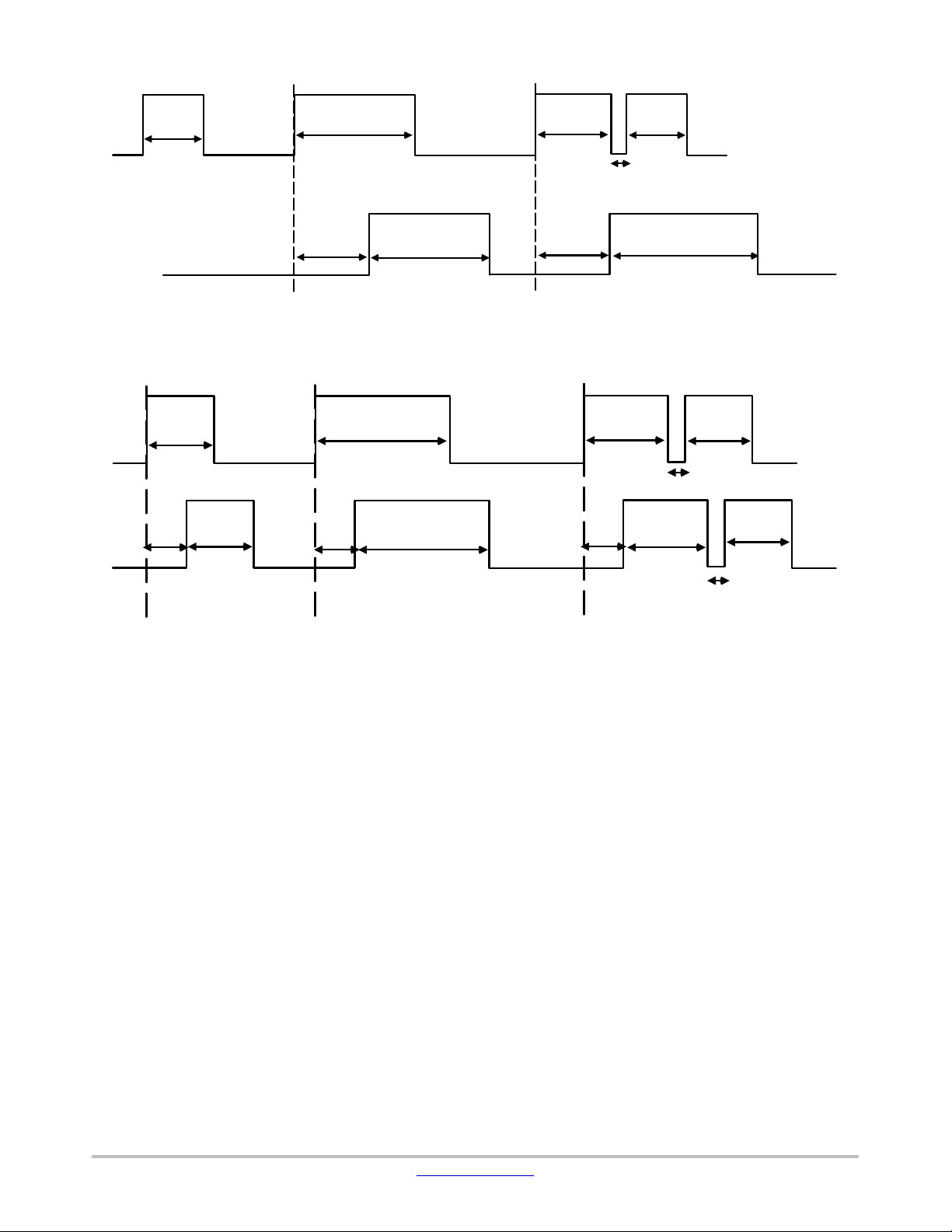
NCP51530A features a noise rejection function to ensure
that any pulse glitch shorter than 30 ns will not produce any
output. These features are well illustrated in the Figure 26
below.
NCP51530B has no such filters in the input stages. The
timing diagram NCP51530B is Figure 27 below.
and VB voltage levels. The
CC
Table 7. INPUT TABLE
S.No LIN HIN LO HO
1 0 0 0 0
2 0 1 0 1
3 1 0 1 0
4 1 1 1 1
5 X 0 0 0
6 X 1 0 1
7 X X 0 0
8 0 X 0 0
9 1 X 1 0
www.onsemi.com
13
Page 14
NCP51530
30ns
25ns
30ns
30ns
80ns
LIN/HIN
60ns
LO /HO
80ns
Figure 26. Input Filter (NCP51530A)
80ns
LIN/HIN
25ns
80ns
50ns
60ns
25ns
10ns
50ns
40ns
50ns
100ns
40ns
10ns
40ns
Figure 27. No Input Filter (NCP51530B)
10ns
www.onsemi.com
14
Page 15

VCCON
V
CC
OFF
V
LIN
NCP51530
CC
V
VB − V
B
LO
ON
HB
HIN
HO
Figure 28. UVLO Timing Diagram
UNDER VOLTAGE LOCK−OUT
NCP51530 has under voltage lockout protection on both
the high side and the low side driver. The function of the
UVLO circuits is to ensure that there is enough supply
voltages (V
and VB) to correctly bias high side and low
CC
side circuits. This also ensures that the gate of external
MOSFETs are driven at an optimum voltage.
www.onsemi.com
If the V
is below the VCC UVLO voltage, the low side
CC
driver output (LO) and high side driver output (HO) both
remain low.
If VB is below VB UVLO voltage the high side driver
output (HO) remains low. However if the V
is above V
CC
UVLO voltage level, the low side driver output (LO) can
still turn on and off based on the low side driver input (LI)
15
CC
Page 16
NCP51530
and is not affected by the VB status. This ensures proper
charging of the bootstrap capacitor to bring the high side bias
supply V
Both the V
above UVLO voltage.
B
CC
and V
UVLO circuits are provided with
B
hysteresis feature. This hysteresis feature avoids errors due
to ground noise in the power supply. The hysteresis also
ensures continuous operation in case of a small drop in the
bias voltage. This drop in the bias can happen when device
starts switching MOSFET and the operating current of the
device increases. The UVLO feature of the device is
explained in the Figure 28.
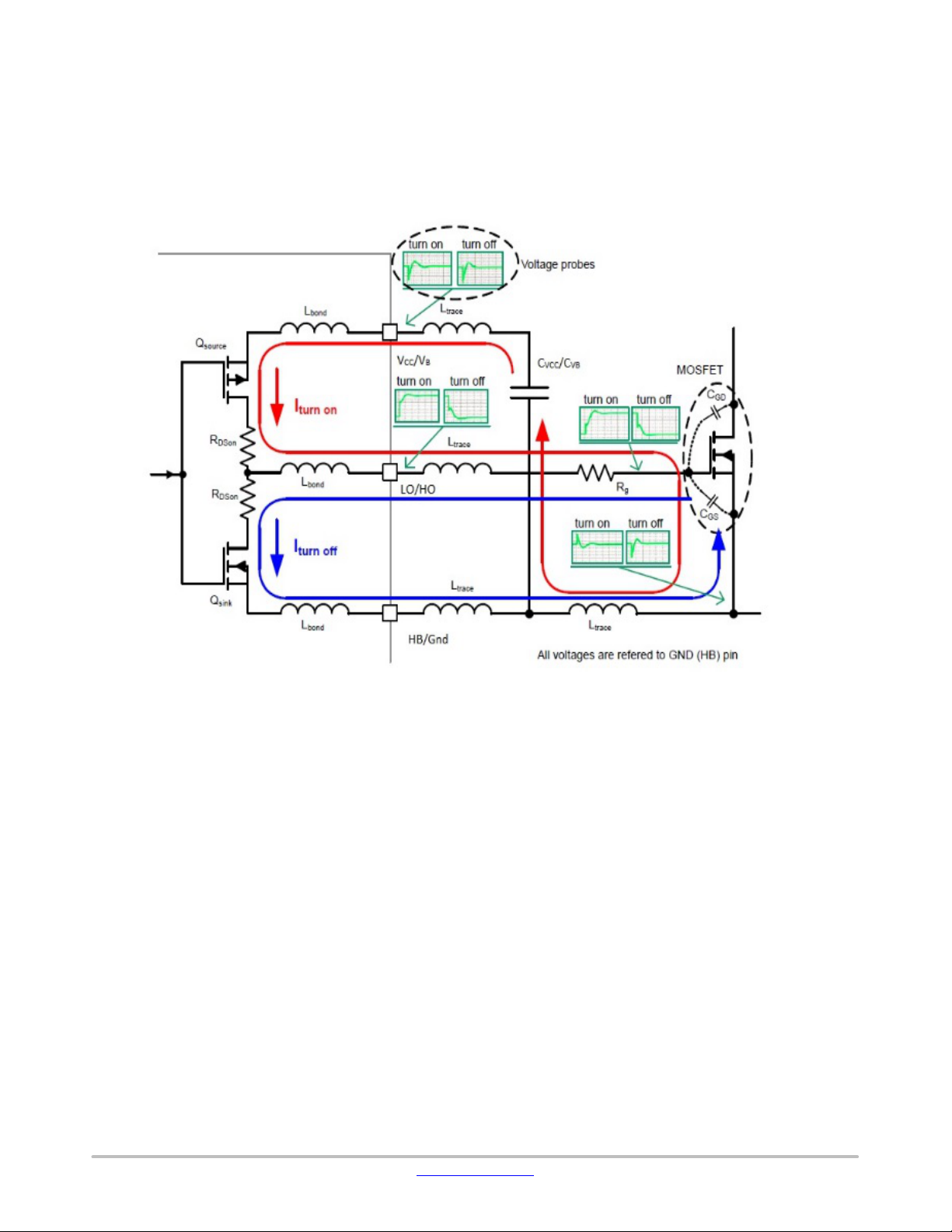
Figure 29. NCP51530 Turn ON−OFF Paths
OUTPUT STAGES
The NCP51530 is equipped with two independent drivers.
The output stage of NCP51530 has 3.5 A/3 A current
source/sink capability which can effectively charge and
discharge a 1 nF load in 15 ns.
The outputs of NCP51530 can be turned on at the same
time and there is no internal dead−time built between them.
This allows NCP51530 to be used in topologies like two
switch forward converter.
The figure below show the output stage structure and the
charging and discharging path of the external power
MOSFET. The bias supply V
CC
or V
supply the energy to
B
charge the gate capacitance Cgs of the low side or the top
side external MOSFETs respectively. When a logic high is
received from input stage, Qsource turns on and V
CC/VB
starts charging Cgs through Rg. Once the Cgs is charged to
the drive voltage level the external power MOSFET turns on
the external MOSFET to discharge to GND/HB level.
When a logic low signal is received from the input stage,
Qsource turns off and Qsink turns on providing a path for
gate terminal of
As seen in the figure, there are parasitic inductances in
charging and discharging path of the Cgs. This can result in
a little dip in the bias voltages V
. If the VCC/VB drops
CC/VB
below UVLO the power supply can shut down the device.
www.onsemi.com
16
Page 17

NCP51530
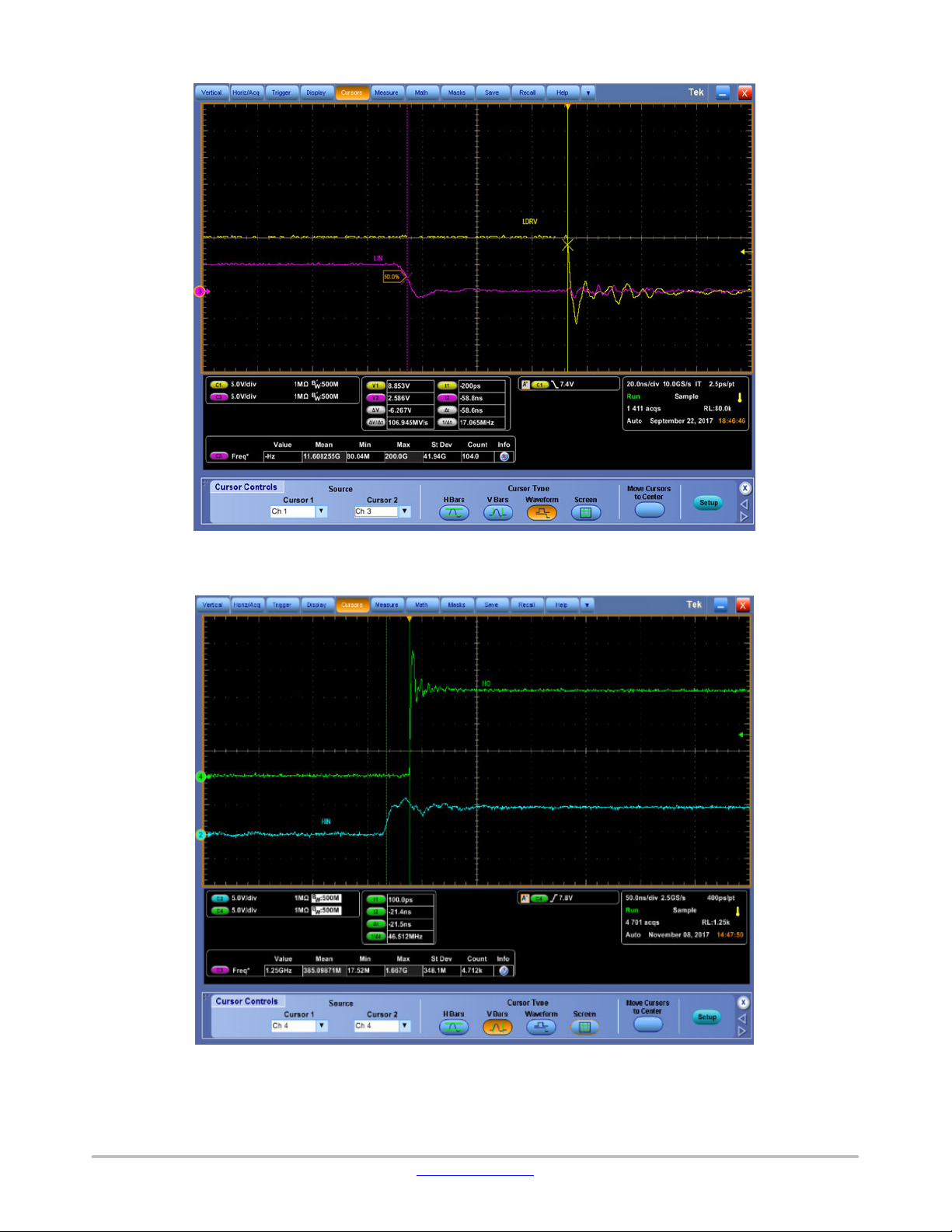
Figure 30. Low Side Turn−ON Propagation Delay (NCP51530A)
FAST PROPAGATION DELAY
NCP51530 boasts of industry best propagation delay
between input and output. NCP51530A has a typical of
60 ns propagation delay. The best in class propagation delay
in NCP51530 makes it suitable for high frequency
operation.
Since NCP51530B doesn’t have the input filter included,
the propagation delay are even faster. NCP51530B offers
25 ns propagation delay between input and output.
www.onsemi.com
17
Page 18
NCP51530
Figure 31. Low Side Turn−Off Propagation Delay (NCP51530A)
Figure 32. High Side Turn−Off Propagation Delay (NCP51530B)
www.onsemi.com
18
Page 19

NCP51530
Figure 33. High Side Turn−Off Propagation Delay (NCP51530B)
www.onsemi.com
19
Page 20

NCP51530
Figure 34. Bootstrap Circuit
COMPONENT SELECTION
C
CAPACITOR VALUE CALCULATION
BOOT
NCP51530 has two independent drivers for driving high
side and low side external MOSFETs. The bias for the high
side driver is usually provided through a bootstrap circuit. A
typical bootstrap circuit is shown in the figure 8 below.
The high side driver is biased by the C
capacitor). As can be seen in the circuit, C
only when HB goes to GND level. Low value of C
result in a little dip in the bias voltages V
(bootstrap
boot
will charge
boot
boot
. If the VB drops
B
can
below UVLO the power supply can shut down the high side
driver. Therefore choosing the right value of C
boot
is very
important for a robust design.
An example design for C
Qg+ 30 nC, VCC+ 15 V
Qb+ IBQ*t
Q
+ Qg) Qb+ 30 nC ) 405p + 30.4 pC
tot
C
boot
+
V
Q
ripple
discharge
tot
+
is given below.
boot
+ 81 mC*5mS + 405 pC
30.4 nC
150 mV
+ 203 nF
(eq. 1)
(eq. 2)
(eq. 3)
(eq. 4)
Qg is equivalent gate charge of the FET
I
is the boot quiescent current
BQ
t
dishcharge
V
ripple
is the discharge time for bootstrap capacitor
is the allowed ripple voltage in the bootstrap
capacitor
It is recommended to use a larger value so as to cover any
variations in the gate charge and voltage with temperature.
R
RESISTOR VALUE CALCULATION
boot
R
resistor value is very important to ensure proper
boot
function of the device. A high value of R
down the charging of the C
while too low a value would
boot
push very high charging currents for C
a value between 2 W and 10 W is recommended for R
+
boot
V
CC
R
= 5 W
* V
boot
15 V * 1V
D
+
5 W
For example R
I
boot(pk)
Where V
Thus, R
HIN AND LIN INPUT FILTER
is the bootstrap diode forward drop.
D
value of 5 W keeps the peak current below 2.8 A.
boot
would slow
boot
. For NCP51530
boot
+ 2.8 A
boot
(eq. 5)
For PWM connection on the LIN and HIN pin of the
NCP51530, a RC is recommended to filter high frequency
input noise.
This filter is particularly important in case of NCP51530B
where no internal filter is included.
The recommended value for R
LIN/RHIN
and C
HIN/CLIN
are as below.
R
LIN/RHIN
C
HIN/CLIN
= 100 W
= 120 pF
.
www.onsemi.com
20
Page 21

NCP51530
VCC CAPACITOR SELECTION
VCC capacitor value should be selected at least ten times
the value of C
R
SELECTION
gate
R
are selected to limit the peak gate current during
gate
. In this case thus C
boot
VCC
> 2 mF.
charging and discharging of the gate capacitance. This
resistance also helps to damp the ringing due to the parasitic
inductances.
For example for a R
value of 5 W, the peak source and
gate
sink currents would be limited to the following values.
R
I
LO_Source
I
LO_Sink
I
HO_Source
I
HO_Sink
+
+
+
V
R
+
R
CC
Lgate
R
Lgate
V
R
Lgate
Lgate
V
CC
* V
) R
V
) R
CC
) R
* V
) R
Dboot
gate
CC
LOL
Dboot
HOL
+ 5W
+
LOH
+
6.8 W
+
HOH
15 V * 1V
+
15 V
6.7 W
15 V
14 V
6.7 W
6.8 W
+ 2.23 A
+ 2.20 A
+ 2.09 A
+ 2.06 A
(eq. 6)
(eq. 7)
(eq. 8)
(eq. 9)
(eq. 10)
TOTAL POWER DISSIPATION
Total power dissipation of NCP51530 can be calculated as
follows.
1. Static power loss of device (excluding drivers)
while switching at an appropriate frequency.
P
operating
+ V
+ 14 V * 0.4 mA ) 15 V * 0.4 mA + 11.6 mW
*IBO) VCC*I
boot
CCO
IBO is the operating current for the high side driver
I
is the operating current for the low side driver
CCO
2. Power loss of driving external FET (Hard
Switching)
ǒ
P
drivers
+
ǒ
+
Qg*V
ǒ
ǒ
30 nC * 14 VǓ)ǒ30 nC * 15 V
boost
Ǔ
)ǒQg*V
Ǔ
Ǔ
f
CC
Ǔ
Ǔ
* 100 kHz + 87 mW
Qg is total gate charge of the MOSFET
3. Power loss of driving external FET (Soft
Switching)
P
drivers
ǒ
ǒ
+
Qgs*V
ǒ
ǒ
+
4nC*14VǓ)ǒ4nC*15V
boot
Ǔ
)ǒQgs*V
Ǔ
Ǔ
*f
CC
Ǔ
Ǔ
* 100 kHz + 11 mW
4. Level shifting losses
P
levelshifting
+ǒVr) V
+ 415 V * 0.5 nC * 100 kHz + 20.75 mW
Ǔ
*Q*f
b
Vr is the rail voltage
Q is the substrate charge on the level shifter
5. Total Power Loss (Hard Switching)
P
total
+ P
driver
) P
operating
) P
levelshifting
+ 11.6 mW ) 87 mW ) 20.75 mW + 119.35 mW
6. Junction temperature increase
tJ+ R
qJA*Ptotal
+ 183 * 0.14 + 25° C
(eq. 11)
(eq. 12)
(eq. 13)
(eq. 14)
(eq. 15)
(eq. 16)
www.onsemi.com
21
Page 22

NCP51530
LAYOUT RECOMMENDATIONS
NCP51530 is a high speed and high current high side and
low side driver. To avoid any device malfunction during
device operation, it is very important that there is very low
parasitic inductance in the current switching path. It is very
important that the best layout practices are followed for the
PCB layout of the NCP51530. An example layout is shown
in the figure below. Some of the layout rules to be followed
are listed below.
• Keep the low side drive path LO−Q1−GND as small as
possible. This reduces the parasitic inductance in the
path and hence eliminates ringing on the gate terminal
of the low side MOSFET Q1.
• Keep the high side drive loop HO−Q2−HB as small as
possible. This reduces the parasitic inductance in the
path and hence eliminates ringing on the gate terminal
of the low side MOSFET Q1.
• Keep C
V
CC
• Keep C
as near to the VCC pin as possible and the
VCC
−CVCC−GND loop as small as possible.
as near to VB pin as possible and
VB
VB−CVB−HB loop as small as possible.
• Keep the HB−GND−Q1 loop as small as possible. This
loop has the potential to produce a negative voltage
spike on the HB pin. This negative voltage spike can
cause damage to the driver. This negative spike can
increase the boot capacitor voltage above the maximum
rating and hence cause damage to the driver.
Figure 35. Example Layout
ORDERING INFORMATION
Propagation Delay
Device
NCP51530ADR2G 60 Yes
NCP51530BDR2G 25 No
NCP51530AMNTWG 60 Ye s
NCP51530BMNTWG 25 No
†For information on tape and reel specifications, including part orientation and tape sizes, please refer to our Tape and Reel Packaging
Specification Brochure, BRD8011/D.
(ns)
Input filter Package Shipping
SOIC−8
(Pb−Free)
SOIC−8
(Pb−Free)
DFN10 4x4
(Pb−Free)
DFN10 4x4
(Pb−Free)
www.onsemi.com
22
2500 / Tape & Reel
2500 / Tape & Reel
4000 / Tape & Reel
4000 / Tape & Reel
†
Page 23

MECHANICAL CASE OUTLINE
PACKAGE DIMENSIONS
1
SCALE 2:1
B
A3
5
A1
6
A
E
A
C
0.10 C A
10X
L
E2
10X
b
0.10 C
0.05 C
10X
0.60
PIN ONE
REFERENCE
2X
2X
10X
NOTE 4
DETAIL A
E3
C0.10
C0.10
TOP VIEW
C0.10
C0.08
SIDE VIEW
1
K
10
e
BOTTOM VIEW
RECOMMENDED
MOUNTING FOOTPRINT
PACKAGE
OUTLINE
D
DETAIL B
D2
3.20
DFN10 4x4, 0.8P
CASE 506DJ
ISSUE O
L
ALTERNATE A−1 ALTERNATE A−2
ALTERNATE TERMINAL
A1
ALTERNATE B−1 ALTERNATE B−2
SEATING
PLANE
B
B
0.10 C A
A
BB
NOTE 3
L1
DETAIL A
CONSTRUCTIONS
A3
DETAIL B
ALTERNATE
CONSTRUCTIONS
B
B
DATE 20 MAY 2016
NOTES:
1. DIMENSIONING AND TOLERANCING PER ASME
Y14.5M, 1994.
L
2. CONTROLLING DIMENSION: MILLIMETERS.
3. DIMENSION b APPLIES TO PLATED TERMINAL AND IS
MEASURED BETWEEN 0.25 AND 0.30 MM FROM THE
TERMINAL TIP.
4. COPLANARITY APPLIES TO THE EXPOSED PAD AS
WELL AS THE TERMINALS.
5. FOR DEVICE OPN CONTAINING W OPTION, DETAIL A
ALTERNATE CONSTRUCTION A−2 AND DETAIL B ALTERNATE CONSTRUCTION B−2 ARE NOT APPLICABLE.
MILLIMETERS
DIM MIN MAX
MOLD CMPDEXPOSED Cu
A 0.80 1.00
A1 0.00 0.05
A3 0.20 REF
b 0.25 0.35
D 4.00 BSC
D2 2.90 3.10
E 4.00 BSC
E2 1.85 2.05
E3
0.375 BSC
e 0.80 BSC
K 0.90 −−−
L 0.35 0.45
L1 0.00 0.15
GENERIC
MARKING DIAGRAM*
XXXXXX
XXXXXX
ALYWG
G
XXXXX = Specific Device Code
A = Assembly Location
L = Wafer Lot
Y = Year
W = Work Week
G = Pb−Free Package
(Note: Microdot may be in either location)
*This information is generic. Please refer
to device data sheet for actual part
marking. Pb−Free indicator, “G”, may
or not be present.
4.30
0.75
2.15
1
0.80
PITCH
DOCUMENT NUMBER:
DESCRIPTION:
ON Semiconductor and are trademarks of Semiconductor Components Industries, LLC dba ON Semiconductor or its subsidiaries in the United States and/or other countries.
ON Semiconductor reserves the right to make changes without further notice to any products herein. ON Semiconductor makes no warranty, representation or guarantee regarding
the suitability of its products for any particular purpose, nor does ON Semiconductor assume any liability arising out of the application or use of any product or circuit, and specifically
disclaims any and all liability, including without limitation special, consequential or incidental damages. ON Semiconductor does not convey any license under its patent rights nor the
rights of others.
© Semiconductor Components Industries, LLC, 2019
DIMENSIONS: MILLIMETERS
98AON12037G
DFN10 4X4, 0.8P
10X
0.42
Electronic versions are uncontrolled except when accessed directly from the Document Repository.
Printed versions are uncontrolled except when stamped “CONTROLLED COPY” in red.
PAGE 1 OF 1
www.onsemi.com
Page 24

MECHANICAL CASE OUTLINE
PACKAGE DIMENSIONS
8
1
SCALE 1:1
−Y−
−Z−
−X−
A
58
B
1
4
G
H
D
0.25 (0.010) Z
M
SOLDERING FOOTPRINT*
7.0
0.275
S
Y
0.25 (0.010)
C
SEATING
PLANE
SXS
0.060
0.10 (0.004)
1.52
4.0
0.155
CASE 751−07
M
M
Y
N
SOIC−8 NB
ISSUE AK
K
X 45
_
M
J
MARKING DIAGRAM*
8
XXXXX
ALYWX
1
XXXXX = Specific Device Code
A = Assembly Location
L = Wafer Lot
Y = Year
W = Work Week
G = Pb−Free Package
8
XXXXX
ALYWX
G
1
IC
IC
(Pb−Free)
DATE 16 FEB 2011
NOTES:
1. DIMENSIONING AND TOLERANCING PER
ANSI Y14.5M, 1982.
2. CONTROLLING DIMENSION: MILLIMETER.
3. DIMENSION A AND B DO NOT INCLUDE
MOLD PROTRUSION.
4. MAXIMUM MOLD PROTRUSION 0.15 (0.006)
PER SIDE.
5. DIMENSION D DOES NOT INCLUDE DAMBAR
PROTRUSION. ALLOWABLE DAMBAR
PROTRUSION SHALL BE 0.127 (0.005) TOTAL
IN EXCESS OF THE D DIMENSION AT
MAXIMUM MATERIAL CONDITION.
6. 751−01 THRU 751−06 ARE OBSOLETE. NEW
STANDARD IS 751−07.
MILLIMETERS
DIMAMIN MAX MIN MAX
4.80 5.00 0.189 0.197
B 3.80 4.00 0.150 0.157
C 1.35 1.75 0.053 0.069
D 0.33 0.51 0.013 0.020
G 1.27 BSC 0.050 BSC
H 0.10 0.25 0.004 0.010
J 0.19 0.25 0.007 0.010
K 0.40 1.27 0.016 0.050
M 0 8 0 8
____
N 0.25 0.50 0.010 0.020
S 5.80 6.20 0.228 0.244
INCHES
GENERIC
8
XXXXXX
AYWW
1
Discrete
XXXXXX = Specific Device Code
A = Assembly Location
Y = Year
WW = Work Week
G = Pb−Free Package
8
XXXXXX
AYWW
1
Discrete
(Pb−Free)
G
0.6
0.024
1.270
0.050
SCALE 6:1
ǒ
inches
mm
Ǔ
*This information is generic. Please refer to
device data sheet for actual part marking.
Pb−Free indicator, “G” or microdot “G”, may
or may not be present. Some products may
not follow the Generic Marking.
*For additional information on our Pb−Free strategy and soldering
details, please download the ON Semiconductor Soldering and
Mounting Techniques Reference Manual, SOLDERRM/D.
STYLES ON PAGE 2
DOCUMENT NUMBER:
DESCRIPTION:
ON Semiconductor and are trademarks of Semiconductor Components Industries, LLC dba ON Semiconductor or its subsidiaries in the United States and/or other countries.
ON Semiconductor reserves the right to make changes without further notice to any products herein. ON Semiconductor makes no warranty, representation or guarantee regarding
the suitability of its products for any particular purpose, nor does ON Semiconductor assume any liability arising out of the application or use of any product or circuit, and specifically
disclaims any and all liability, including without limitation special, consequential or incidental damages. ON Semiconductor does not convey any license under its patent rights nor the
rights of others.
© Semiconductor Components Industries, LLC, 2019
98ASB42564B
SOIC−8 NB
Electronic versions are uncontrolled except when accessed directly from the Document Repository.
Printed versions are uncontrolled except when stamped “CONTROLLED COPY” in red.
PAGE 1 OF 2
www.onsemi.com
Page 25

STYLE 1:
PIN 1. EMITTER
2. COLLECTOR
3. COLLECTOR
4. EMITTER
5. EMITTER
6. BASE
7. BASE
8. EMITTER
STYLE 5:
PIN 1. DRAIN
2. DRAIN
3. DRAIN
4. DRAIN
5. GATE
6. GATE
7. SOURCE
8. SOURCE
STYLE 9:
PIN 1. EMITTER, COMMON
2. COLLECTOR, DIE #1
3. COLLECTOR, DIE #2
4. EMITTER, COMMON
5. EMITTER, COMMON
6. BASE, DIE #2
7. BASE, DIE #1
8. EMITTER, COMMON
STYLE 13:
PIN 1. N.C.
2. SOURCE
3. SOURCE
4. GATE
5. DRAIN
6. DRAIN
7. DRAIN
8. DRAIN
STYLE 17:
PIN 1. VCC
2. V2OUT
3. V1OUT
4. TXE
5. RXE
6. VEE
7. GND
8. ACC
STYLE 21:
PIN 1. CATHODE 1
2. CATHODE 2
3. CATHODE 3
4. CATHODE 4
5. CATHODE 5
6. COMMON ANODE
7. COMMON ANODE
8. CATHODE 6
STYLE 25:
PIN 1. VIN
2. N/C
3. REXT
4. GND
5. IOUT
6. IOUT
7. IOUT
8. IOUT
STYLE 29:
PIN 1. BASE, DIE #1
2. EMITTER, #1
3. BASE, #2
4. EMITTER, #2
5. COLLECTOR, #2
6. COLLECTOR, #2
7. COLLECTOR, #1
8. COLLECTOR, #1
STYLE 2:
PIN 1. COLLECTOR, DIE, #1
2. COLLECTOR, #1
3. COLLECTOR, #2
4. COLLECTOR, #2
5. BASE, #2
6. EMITTER, #2
7. BASE, #1
8. EMITTER, #1
STYLE 6:
PIN 1. SOURCE
2. DRAIN
3. DRAIN
4. SOURCE
5. SOURCE
6. GATE
7. GATE
8. SOURCE
STYLE 10:
PIN 1. GROUND
2. BIAS 1
3. OUTPUT
4. GROUND
5. GROUND
6. BIAS 2
7. INPUT
8. GROUND
STYLE 14:
PIN 1. N−SOURCE
2. N−GATE
3. P−SOURCE
4. P−GATE
5. P−DRAIN
6. P−DRAIN
7. N−DRAIN
8. N−DRAIN
STYLE 18:
PIN 1. ANODE
2. ANODE
3. SOURCE
4. GATE
5. DRAIN
6. DRAIN
7. CATHODE
8. CATHODE
STYLE 22:
PIN 1. I/O LINE 1
2. COMMON CATHODE/VCC
3. COMMON CATHODE/VCC
4. I/O LINE 3
5. COMMON ANODE/GND
6. I/O LINE 4
7. I/O LINE 5
8. COMMON ANODE/GND
STYLE 26:
PIN 1. GND
2. dv/dt
3. ENABLE
4. ILIMIT
5. SOURCE
6. SOURCE
7. SOURCE
8. VCC
STYLE 30:
PIN 1. DRAIN 1
2. DRAIN 1
3. GATE 2
4. SOURCE 2
5. SOURCE 1/DRAIN 2
6. SOURCE 1/DRAIN 2
7. SOURCE 1/DRAIN 2
8. GATE 1
SOIC−8 NB
CASE 751−07
ISSUE AK
STYLE 3:
STYLE 7:
STYLE 11:
STYLE 15:
PIN 1. DRAIN, DIE #1
2. DRAIN, #1
3. DRAIN, #2
4. DRAIN, #2
5. GATE, #2
6. SOURCE, #2
7. GATE, #1
8. SOURCE, #1
PIN 1. INPUT
2. EXTERNAL BYPASS
3. THIRD STAGE SOURCE
4. GROUND
5. DRAIN
6. GATE 3
7. SECOND STAGE Vd
8. FIRST STAGE Vd
PIN 1. SOURCE 1
2. GATE 1
3. SOURCE 2
4. GATE 2
5. DRAIN 2
6. DRAIN 2
7. DRAIN 1
8. DRAIN 1
PIN 1. ANODE 1
2. ANODE 1
3. ANODE 1
4. ANODE 1
5. CATHODE, COMMON
6. CATHODE, COMMON
7. CATHODE, COMMON
8. CATHODE, COMMON
STYLE 19:
PIN 1. SOURCE 1
2. GATE 1
3. SOURCE 2
4. GATE 2
5. DRAIN 2
6. MIRROR 2
7. DRAIN 1
8. MIRROR 1
STYLE 23:
PIN 1. LINE 1 IN
2. COMMON ANODE/GND
3. COMMON ANODE/GND
4. LINE 2 IN
5. LINE 2 OUT
6. COMMON ANODE/GND
7. COMMON ANODE/GND
8. LINE 1 OUT
STYLE 27:
PIN 1. ILIMIT
2. OVLO
3. UVLO
4. INPUT+
5. SOURCE
6. SOURCE
7. SOURCE
8. DRAIN
DATE 16 FEB 2011
STYLE 4:
PIN 1. ANODE
2. ANODE
3. ANODE
4. ANODE
5. ANODE
6. ANODE
7. ANODE
8. COMMON CATHODE
STYLE 8:
PIN 1. COLLECTOR, DIE #1
2. BASE, #1
3. BASE, #2
4. COLLECTOR, #2
5. COLLECTOR, #2
6. EMITTER, #2
7. EMITTER, #1
8. COLLECTOR, #1
STYLE 12:
PIN 1. SOURCE
2. SOURCE
3. SOURCE
4. GATE
5. DRAIN
6. DRAIN
7. DRAIN
8. DRAIN
STYLE 16:
PIN 1. EMITTER, DIE #1
2. BASE, DIE #1
3. EMITTER, DIE #2
4. BASE, DIE #2
5. COLLECTOR, DIE #2
6. COLLECTOR, DIE #2
7. COLLECTOR, DIE #1
8. COLLECTOR, DIE #1
STYLE 20:
PIN 1. SOURCE (N)
2. GATE (N)
3. SOURCE (P)
4. GATE (P)
5. DRAIN
6. DRAIN
7. DRAIN
8. DRAIN
STYLE 24:
PIN 1. BASE
2. EMITTER
3. COLLECTOR/ANODE
4. COLLECTOR/ANODE
5. CATHODE
6. CATHODE
7. COLLECTOR/ANODE
8. COLLECTOR/ANODE
STYLE 28:
PIN 1. SW_TO_GND
2. DASIC_OFF
3. DASIC_SW_DET
4. GND
5. V_MON
6. VBULK
7. VBULK
8. VIN
DOCUMENT NUMBER:
DESCRIPTION:
ON Semiconductor and are trademarks of Semiconductor Components Industries, LLC dba ON Semiconductor or its subsidiaries in the United States and/or other countries.
ON Semiconductor reserves the right to make changes without further notice to any products herein. ON Semiconductor makes no warranty, representation or guarantee regarding
the suitability of its products for any particular purpose, nor does ON Semiconductor assume any liability arising out of the application or use of any product or circuit, and specifically
disclaims any and all liability, including without limitation special, consequential or incidental damages. ON Semiconductor does not convey any license under its patent rights nor the
rights of others.
© Semiconductor Components Industries, LLC, 2019
98ASB42564B
SOIC−8 NB
Electronic versions are uncontrolled except when accessed directly from the Document Repository.
Printed versions are uncontrolled except when stamped “CONTROLLED COPY” in red.
PAGE 2 OF 2
www.onsemi.com
Page 26

ON Semiconductor and are trademarks of Semiconductor Components Industries, LLC dba ON Semiconductor or its subsidiaries in the United States and/or other countries.
ON Semiconductor owns the rights to a number of patents, trademarks, copyrights, trade secrets, and other intellectual property. A listing of ON Semiconductor’s product/patent
coverage may be accessed at www.onsemi.com/site/pdf/Patent−Marking.pdf
ON Semiconductor makes no warranty, representation or guarantee regarding the suitability of its products for any particular purpose, nor does ON Semiconductor assume any liability
arising out of the application or use of any product or circuit, and specifically disclaims any and all liability, including without limitation special, consequential or incidental damages.
Buyer is responsible for its products and applications using ON Semiconductor products, including compliance with all laws, regulations and safety requirements or standards,
regardless of any support or applications information provided by ON Semiconductor. “Typical” parameters which may be provided in ON Semiconductor data sheets and/or
specifications can and do vary in different applications and actual performance may vary over time. All operating parameters, including “Typicals” must be validated for each customer
application by customer’s technical experts. ON Semiconductor does not convey any license under its patent rights nor the rights of others. ON Semiconductor products are not
designed, intended, or authorized for use as a critical component in life support systems or any FDA Class 3 medical devices or medical devices with a same or similar classification
in a foreign jurisdiction or any devices intended for implantation in the human body. Should Buyer purchase or use ON Semiconductor products for any such unintended or unauthorized
application, Buyer shall indemnify and hold ON Semiconductor and its officers, employees, subsidiaries, affiliates, and distributors harmless against all claims, costs, damages, and
expenses, and reasonable attorney fees arising out of, directly or indirectly, any claim of personal injury or death associated with such unintended or unauthorized use, even if such
claim alleges that ON Semiconductor was negligent regarding the design or manufacture of the part. ON Semiconductor is an Equal Opportunity/Affirmative Action Employer. This
literature is subject to all applicable copyright laws and is not for resale in any manner.
. ON Semiconductor reserves the right to make changes without further notice to any products herein.
PUBLICATION ORDERING INFORMATION
LITERATURE FULFILLMENT:
Email Requests to: orderlit@onsemi.com
ON Semiconductor Website: www.onsemi.com
TECHNICAL SUPPORT
North American Technical Support:
Voice Mail: 1 800−282−9855 Toll Free USA/Canada
Phone: 011 421 33 790 2910
Europe, Middle East and Africa Technical Support:
Phone: 00421 33 790 2910
For additional information, please contact your local Sales Representative
◊
www.onsemi.com
1
 Loading...