

Page 1
NCP336, NCP337
Controlled Load Switch with
Auto-Discharge Path, 3 A
Description
The NCP336 and NCP337 are very low Ron MOSFET controlled
by external logic pin, allowing optimization of battery life, and
ortable device autonomy.
p
Indeed, thanks to a current consumption optimization with PMOS
structure, leakage currents are eliminated by isolating connected IC on
the battery when not used.
Output discharge path is also embedded to eliminate residual
voltages on the output rail for the NCP337 part only.
Proposed in a wide input voltage range from 1.2 V to 5.5 V, in a
small 1 x 1.5 mm WLCSP6, pitch 0.5 mm.
http://onsemi.com
WLCSP6
FC SUFFIX
CASE 567FH
Features
• 1.2 V − 5.5 V Operating Range
• 21 mW P MOSFET at 4.5 V
• DC Current up to 3 A
• Output Auto−Discharge
• Active High EN Pin
• WLCSP6 1 x 1.5 mm
• This Device is Pb−Free, Halogen Free/BFR Free and is RoHS
Compliant
Applications
• Mobile Phones
• Tablets
• Digital Cameras
• GPS
• Portable Devices
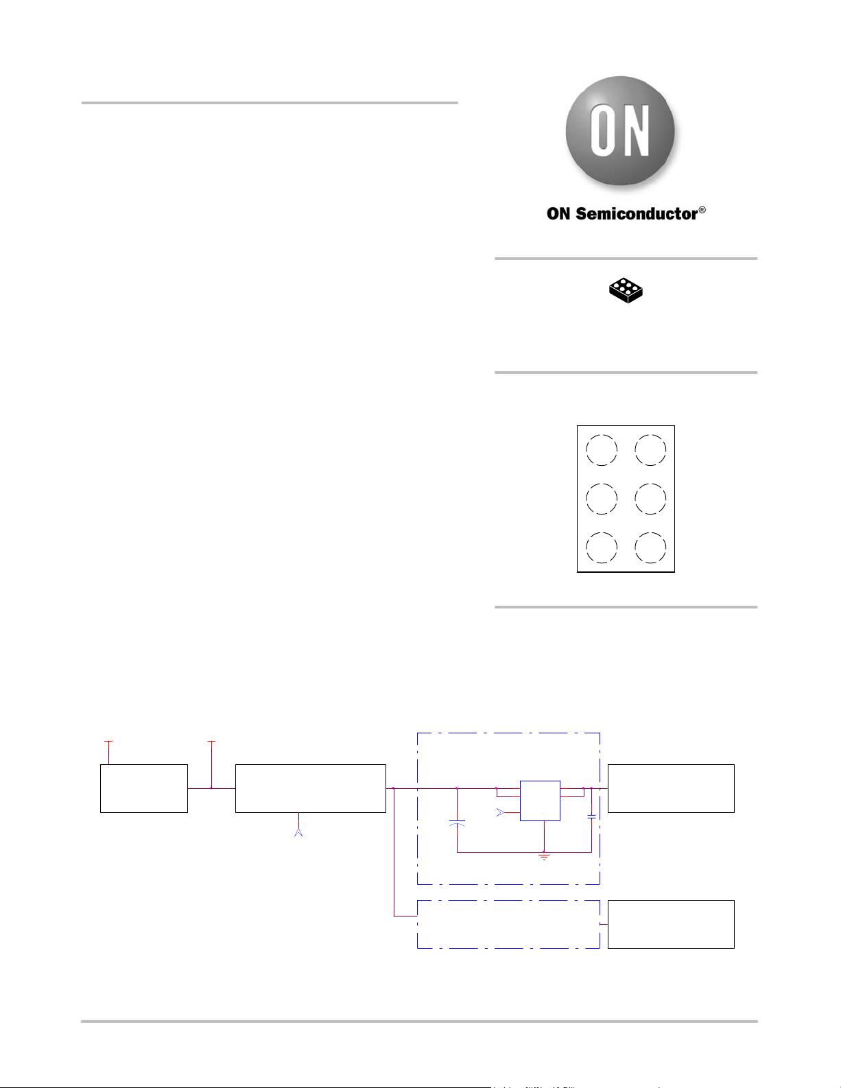
VCC
SMPS
V+
DCDC Converter
or
LDO
ENx
LS
1μF
PIN CONNECTIONS
21
A
B
C
OUT
OUT
GND
(Top View)
IN
IN
EN
ORDERING INFORMATION
See detailed ordering and shipping information on page 8 of
this data sheet.
NCP336 or NCP337
ENy
A2
IN
B2
IN
C2
EN
OUT
OUT
C1
GND
0
A1
B1
100n
Platform IC’n
© Semiconductor Components Industries, LLC, 2012
September, 2012 − Rev. 2
LS
Figure 1. Typical Application Circuit
1 Publication Order Number:
Platform IC’n+1
NCP336/D
Page 2
NCP336, NCP337
Table 1. PIN FUNCTION DESCRIPTION
Pin Name Pin Number Type Description
IN A2, B2 POWER
GND C1 POWER Ground connection.
EN C2 INPUT Enable input, logic high turns on power switch.
OUT A1, B1 OUTPUT
Load−switch input voltage; connect a 1 mF or greater ceramic capacitor from IN to GND
as close as possible to the IC.
Load−switch output; connect a 1 mF ceramic capacitor from OUT to GND as close as
possible to the IC is recommended.
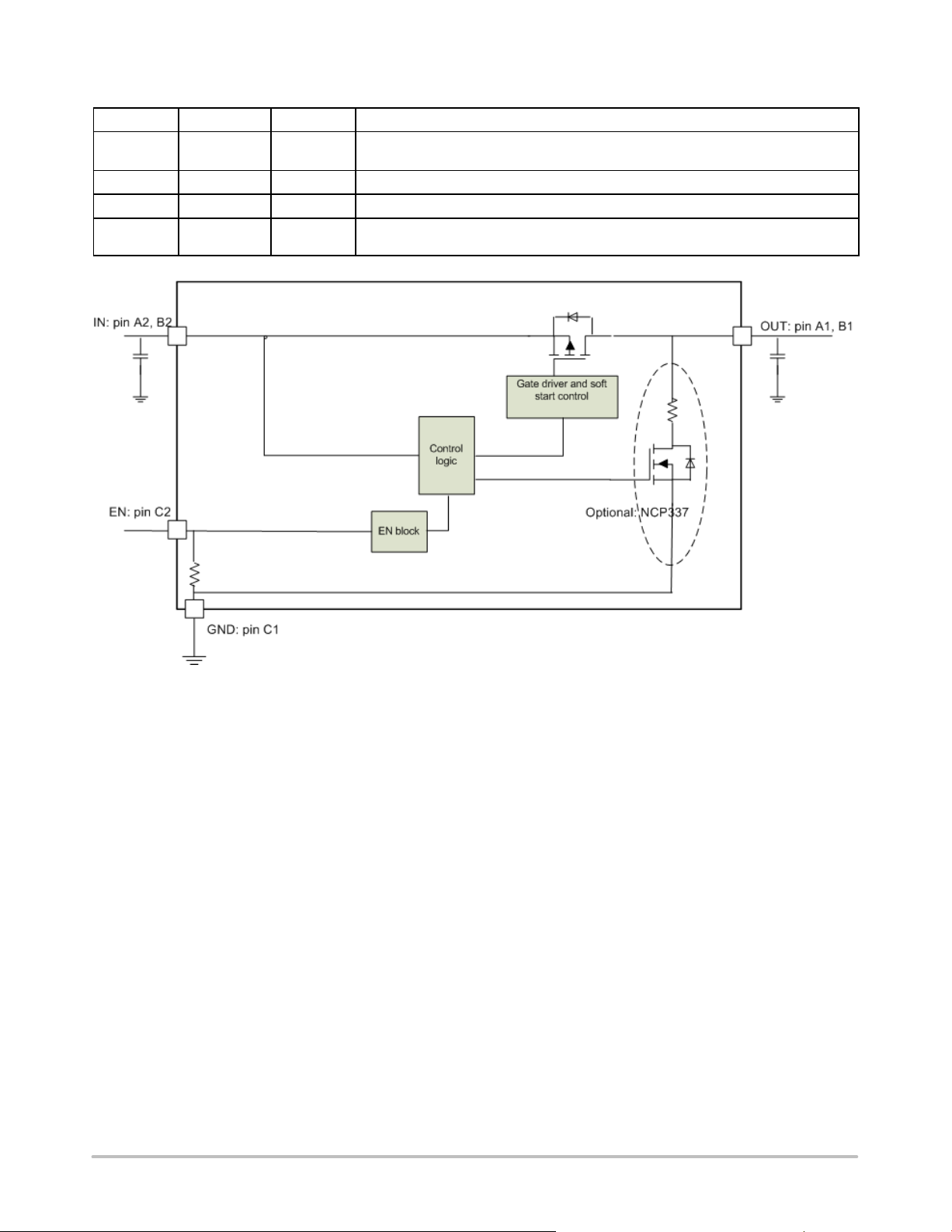
Figure 2. Block Diagram
http://onsemi.com
2
Page 3
NCP336, NCP337
Table 2. MAXIMUM RATINGS
Rating Symbol Value Unit
IN, OUT, EN, Pins: (Note 1) V
From IN to OUT Pins: Input/Output (Note 1) V
Maximum Junction Temperature T
Storage Temperature Range T
Moisture Sensitivity (Note 2) MSL Level 1
Stresses exceeding Maximum Ratings may damage the device. Maximum Ratings are stress ratings only. Functional operation above the
Recommended Operating Conditions is not implied. Extended exposure to stresses above the Recommended Operating Conditions may affect
device reliability.
Table 3. OPERATING CONDITIONS
Symbol Parameter Conditions Min Typ Max Unit
V
IN
V
EN
T
A
T
J
C
IN
C
OUT
R
q
JA
I
OUT
P
D
1. According to JEDEC standard JESD22−A108.
2. Moisture Sensitivity Level (MSL): 1 per IPC/JEDEC standard: J−STD−020.
3. The R
4. The maximum power dissipation (
q
PD+
Operational Power Supply 1.2 5.5 V
Enable Voltage 0 5.5
Ambient Temperature Range −40 25 +85 °C
Junction Temperature Range −40 25 +125 °C
Decoupling input capacitor 1
Decoupling output capacitor 1
Thermal Resistance Junction to Air WLCSP package (Note 3) 100 °C/W
Maximum DC current 3 A
Power Dissipation Rating (Note 4)
TA ≤ 25°C WLCSP package 0.66 W
TA = 85°C WLCSP package 0.26 W
is dependent of the PCB heat dissipation and thermal via.
JA
T
* T
JMAX
A
R
qJA
) is given by the following formula:
PD
EN, VIN,
IN,
STG
V
OUT
J
V
OUT
−0.3 to + 7.0 V
0 to + 7.0 V
−40 to + 125 °C
−40 to + 150 °C
mF
mF
http://onsemi.com
3
Page 4

NCP336, NCP337
Table 4. ELECTRICAL CHARACTERISTIC Min & Max Limits apply for T
(Unless otherwise noted). Typical values are referenced to T
Symbol
Parameter Conditions Min Typ Max Unit
= +25°C and VIN = 5 V (Unless otherwise noted).
A
between −40°C to +85°C for VIN between 1.2 V to 5.5 V
A
POWER SWITCH
R
DSON
Static drain−source
on−state resistance
Vin = 5.5 V I = 1 A (Note 5) 20 22 mW
Vin = 4.5 V I = 500 mA (Note 5) 21 25
Vin = 3.3 V I = 500 mA (Note 5) 23 28
Vin = 2.5 V I = 500 mA (Note 5) 28 35
Vin = 1.8 V I = 250 mA (Note 5) 40 45
Vin = 1.2 V TA = 25°C, I = 200 mA 95 120
Rdis Output discharge path EN = low 70 90
V
IH
V
IL
R
pd
High−level input voltage 0.9
Low−level input voltage 0.5
EN pull down resistor 5
QUIESCENT CURRENT
Istd
Standby current Vin = 4.2 V EN = low, No load 1
Iq Quiescent current Vin = 4.2 V EN = high, No load 1
TIMINGS
T
EN
T
R
T
ON
T
F
Enable time
Output rise time
ON time (TEN + TR)
Output fall time
Vin = 3.6 V
(Note 6)
RL = 25 W, Cout = 1 mF
RL = 25 W, Cout = 1 mF
RL = 25 W, Cout = 1 mF
NCP337. RL = 25 W, Cout = 1 mF
323 ms
810
1130
42
5. Guaranteed by design and characterization
6. Parameters are guaranteed for C
LOAD
and R
connected to the OUT pin with respect to the ground
LOAD
W
V
MW
mA
mA
Vin
EN
Vout
TIMINGS
T
EN
T
R
T
ON
Figure 3. Enable, Rise and Fall Time
T
T
DIS
T
F
OFF
http://onsemi.com
4
Page 5

NCP336, NCP337
TYPICAL CHARACTERISTICS
Figure 4. Rdson (mW) vs. Vin (V) Figure 5. Rdson (mW) vs. Iload (A)
Figure 6. Rdson (mW) vs. Temperature (5C) at 100 mA Figure 7. Rdson (mW) vs. Temperature (5C) at 3 A
http://onsemi.com
5
Page 6

NCP336, NCP337
TYPICAL CHARACTERISTICS
Figure 8. Standby (mA) and Leakage Current (mA)
vs. Vin (V)
Figure 9. Standby Current (mA) vs.
Temperature (5C)
Figure 10. Leakage Current (mA) vs.
Temperature (5C)
Figure 11. Quiescent Current (mA) vs.
Temperature (5C)
http://onsemi.com
6
Page 7

NCP336, NCP337
Figure 12. Enable Time and Rise Time
Figure 13. Disable Time and Fall Time
FUNCTIONAL DESCRIPTION
Overview
The NCP337 is a high side P channel MOSFET power
distribution switch designed to isolate ICs connected on the
battery in order to save energy. The part can be turned on,
with a wide range of battery from 1.2 V to 5.5 V.
Enable Input
Enable pin is an active high. The path is opened when EN
pin is tied low (disable), forcing P MOS switch off.
The IN/OUT path is activated with a minimum of Vin of
1.2 V and EN forced to high level.
http://onsemi.com
Auto Discharge
NMOS FET is placed between the output pin and GND,
in order to discharge the application capacitor connected on
OUT pin.
The auto−discharge is activated when EN pin is set to low
level (disable state).
The discharge path (Pull down NMOS) stays activated as
long as EN pin is set at low level and Vin > 1.2 V.
In order to limit the current across the internal discharge
Nmosfet, the typical value is set at 70 W.
Cin and Cout Capacitors
IN and OUT, 1 mF, at least, capacitors must be placed as
close as possible the part to for stability improvement.
7
Page 8
NCP336, NCP337
APPLICATION INFORMATION
Power Dissipation
Main contributor in term of junction temperature is the
power dissipation of the power MOSFET. Assuming this,
the power dissipation and the junction temperature in
normal mode can be calculated with the following
equations:
• P
D
= R
DS(on)
x (I
OUT
2
)
PD = Power dissipation (W)
= Power MOSFET on resistance (W)
R
DS(on)
I
= Output current (A)
OUT
• T
= PD x R
J
+ T
JA
A
q
TJ = Junction temperature (°C)
= Package thermal resistance (°C/W)
R
JA
q
T
= Ambient temperature (°C)
A
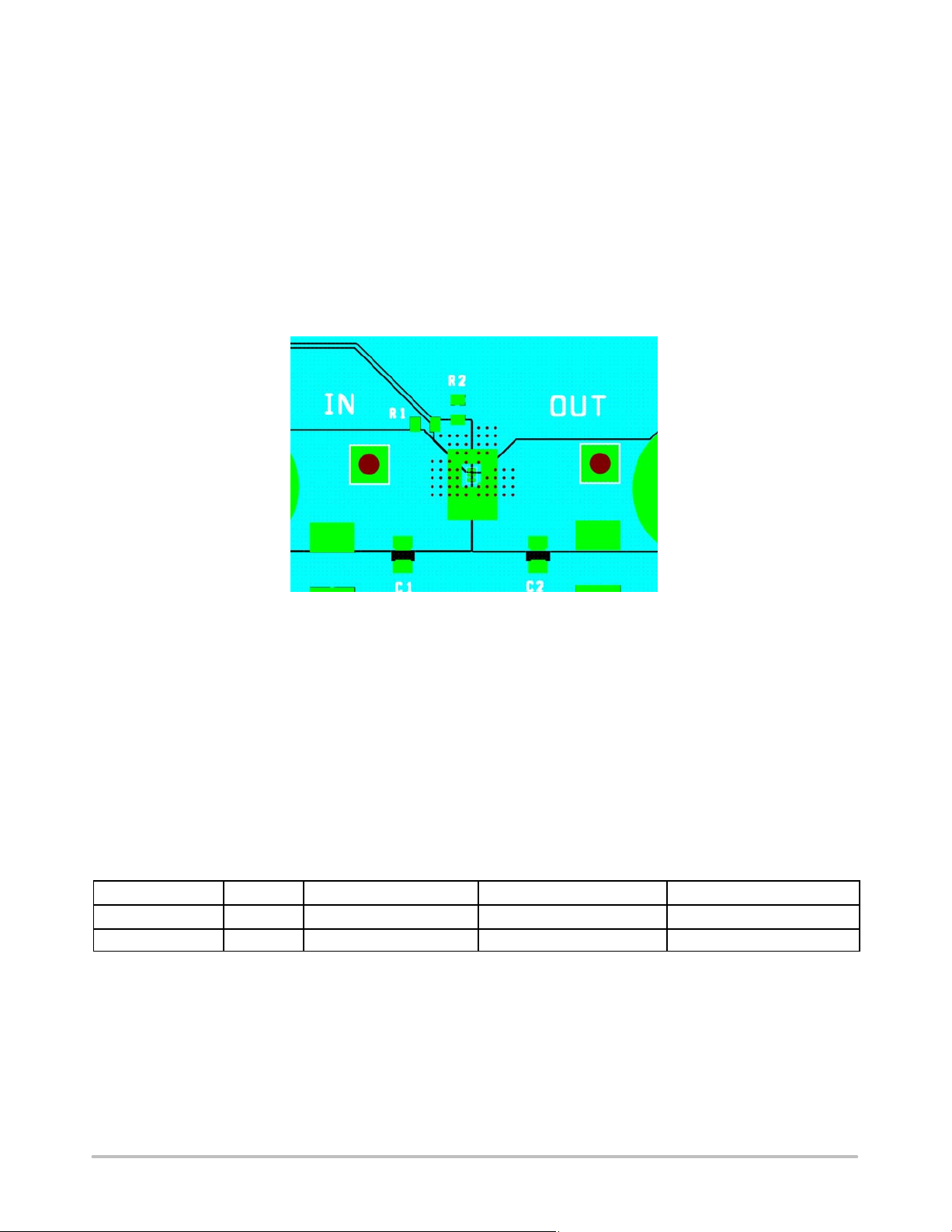
PCB Recommendations
The NCP337 integrates an up to 3 A rated PMOS FET, and
the PCB design rules must be respected to properly evacuate
the heat out of the silicon. By increasing PCB area,
especially around IN and OUT pins, the R
of the package
JA
q
can be decreased, allowing higher power dissipation.
Figure 14. Routing Example: 2 oz, 4 layers with vias across 2 internal inners.
Example of application definition.
TJ* TA+ R
PD+ R
qJA
qJA
R
DS(on)
I
2
TJ: junction temperature.
T
: ambient temperature.
A
= Thermal resistance between IC and air, through PCB.
R
q
R
: intrinsic resistance of the IC Mosfet.
DS(on)
I: load DC current.
Taking into account of R
obtain with:
q
• 1 oz, 2 layers: 100°C/W.
ORDERING INFORMATION
Device Marking Option Package Shipping
NCP337FCT2G AC Auto discharge WLCSP 1 x 1.5 mm 3000 Tape / Reel
NCP336FCT2G AF Without Autodischarge WLCSP 1 x 1.5 mm 3000 Tape / Reel
†For information on tape and reel specifications, including part orientation and tape sizes, please refer to our Tape and Reel Packaging
Specifications Brochure, BRD8011/D.
At 3 A, 25°C ambient temperature, R
5 V, the junction temperature will be:
TJ+ TA) Rq PD+ 25 ) (0.024 32) 100 + 43oC
Taking into account of Rq obtain with:
• 2 oz, 4 layers: 60°C/W.
At 3 A, 65°C ambient temperature, R
5 V, the junction temperature will be:
TJ+ TA) Rq PD+ 65 ) (0.024 32) 60 + 78oC
20 mW @ Vin
DS(on)
24 mW @ Vin
DS(on)
†
http://onsemi.com
8
Page 9

MECHANICAL CASE OUTLINE
PACKAGE DIMENSIONS
SCALE 4:1
WLCSP6, 1.00x1.50
CASE 567FH
ISSUE O
DATE 17 APR 2012
REFERENCE
2X
2X
NOTE 3
0.03
PIN A1
0.05 C
0.05 C
6X
A0.05 BC
C
0.05 C
0.05 C
A1
b
D
TOP VIEW
SIDE VIEW
C
B
A
123
BOTTOM VIEW
e/2
e
A
A2
A
B
E
e
C
SEATING
PLANE
NOTES:
1. DIMENSIONING AND TOLERANCING PER
ASME Y14.5M, 1994.
2. CONTROLLING DIMENSION: MILLIMETERS.
3. COPLANARITY APPLIES TO SPHERICAL
CROWNS OF SOLDER BALLS.
MILLIMETERS
DIMAMIN MAX
A1
A2 0.33 REF
b 0.29 0.34
D 1.00 BSC
E
e 0.50 BSC
0.63
0.54
0.22 0.28
1.50 BSC
RECOMMENDED
SOLDERING FOOTPRINT*
PACKAGE
0.50
PITCH
OUTLINE
6X
0.25
A1
0.50
PITCH
DIMENSIONS: MILLIMETERS
*For additional information on our Pb−Free strategy and soldering
details, please download the ON Semiconductor Soldering and
Mounting Techniques Reference Manual, SOLDERRM/D.
DOCUMENT NUMBER:
DESCRIPTION:
ON Semiconductor and are trademarks of Semiconductor Components Industries, LLC dba ON Semiconductor or its subsidiaries in the United States and/or other countries.
ON Semiconductor reserves the right to make changes without further notice to any products herein. ON Semiconductor makes no warranty, representation or guarantee regarding
the suitability of its products for any particular purpose, nor does ON Semiconductor assume any liability arising out of the application or use of any product or circuit, and specifically
disclaims any and all liability, including without limitation special, consequential or incidental damages. ON Semiconductor does not convey any license under its patent rights nor the
rights of others.
© Semiconductor Components Industries, LLC, 2019
98AON79918E
WLCSP6, 1.00X1.50
Electronic versions are uncontrolled except when accessed directly from the Document Repository.
Printed versions are uncontrolled except when stamped “CONTROLLED COPY” in red.
PAGE 1 OF 1
www.onsemi.com
Page 10

ON Semiconductor and are trademarks of Semiconductor Components Industries, LLC dba ON Semiconductor or its subsidiaries in the United States and/or other countries.
ON Semiconductor owns the rights to a number of patents, trademarks, copyrights, trade secrets, and other intellectual property. A listing of ON Semiconductor’s product/patent
coverage may be accessed at www.onsemi.com/site/pdf/Patent−Marking.pdf
ON Semiconductor makes no warranty, representation or guarantee regarding the suitability of its products for any particular purpose, nor does ON Semiconductor assume any liability
arising out of the application or use of any product or circuit, and specifically disclaims any and all liability, including without limitation special, consequential or incidental damages.
Buyer is responsible for its products and applications using ON Semiconductor products, including compliance with all laws, regulations and safety requirements or standards,
regardless of any support or applications information provided by ON Semiconductor. “Typical” parameters which may be provided in ON Semiconductor data sheets and/or
specifications can and do vary in different applications and actual performance may vary over time. All operating parameters, including “Typicals” must be validated for each customer
application by customer’s technical experts. ON Semiconductor does not convey any license under its patent rights nor the rights of others. ON Semiconductor products are not
designed, intended, or authorized for use as a critical component in life support systems or any FDA Class 3 medical devices or medical devices with a same or similar classification
in a foreign jurisdiction or any devices intended for implantation in the human body. Should Buyer purchase or use ON Semiconductor products for any such unintended or unauthorized
application, Buyer shall indemnify and hold ON Semiconductor and its officers, employees, subsidiaries, affiliates, and distributors harmless against all claims, costs, damages, and
expenses, and reasonable attorney fees arising out of, directly or indirectly, any claim of personal injury or death associated with such unintended or unauthorized use, even if such
claim alleges that ON Semiconductor was negligent regarding the design or manufacture of the part. ON Semiconductor is an Equal Opportunity/Affirmative Action Employer. This
literature is subject to all applicable copyright laws and is not for resale in any manner.
. ON Semiconductor reserves the right to make changes without further notice to any products herein.
PUBLICATION ORDERING INFORMATION
LITERATURE FULFILLMENT:
Email Requests to: orderlit@onsemi.com
ON Semiconductor Website: www.onsemi.com
TECHNICAL SUPPORT
North American Technical Support:
Voice Mail: 1 800−282−9855 Toll Free USA/Canada
Phone: 011 421 33 790 2910
Europe, Middle East and Africa Technical Support:
Phone: 00421 33 790 2910
For additional information, please contact your local Sales Representative
◊
www.onsemi.com
1
 Loading...