

Page 1

Cat. No. W348-E1-05
DRT1-COM
GT1 Series
DeviceNet
MULTIPLE I/O TERMINAL
OPER ATION MANUAL
Page 2

DRT1-COM
GT1 Series
DeviceNet
MULTIPLE I/O TERMINAL
Operation Manual
Revised May 2003
Page 3

iv
Page 4

Notice:
r
f
OMRON products are manufactured for use accordin g to proper procedures by a qualified operator
and only for the purposes described in this manual.
The following conventions are used to ind icate and classify pr ecautions in this manual . Always heed
the information provided with them . Failure to heed precautions can result in in jur y to people or damage to property.
!DANGER Indicates an immine ntly hazardous situation whi ch, if not avoided, will result in death or
serious inj ury.
!WARNING Indicates a potentially hazardous situatio n which, if not avoided, could resu lt in death or
serious inj ury.
!Caution Indicates a potentially ha zardous situation which, if not avoided, may result in minor or
moderate injury, or property damage.
OMRON Product References
All OMRON products are capitalized in this manual. The word “Unit” is also capitalized when it refers to
an OMRON product, regardless of whether or not it appears in the proper name of the product.
The abbreviation “Ch,” which ap pears in some displays and on some OMRON produ cts, often means
“word” and is abbreviated “Wd” in documentation in this sense.
The abbreviation “PC” means Programmable Controller and is not used as an abbreviation for anything
else.
Visual Aids
The following headings appear in the left co lumn of the manual to help you locate different types of
information.
Note Indicates information of pa rticular interest for efficient and convenient opera-
tion of the product.
1,2,3... 1. Indicates lists of one sort or another, such as procedures, checklists, etc.
Trademarks and Copyrights
COMBICON is a registered trademark of Phoenix Contact K.K.
DeviceNet is a registered trademark of the Open DeviceNet Vendor Association, Inc.
PowerTap is a registered trademark of the Allen-Bradley Company, Inc.
OMRON, 1998
All rights reserved. No part of this publication may be reproduced, stored in a retrieval system, or tran smit ted, in any form, o
by any means, mechanical, electronic, photocopying, recording, or otherwise, without the prior written permission o
OMRON.
No patent liability is assumed with respect to th e use of the in fo rmation c ontain ed he rein. M oreover, because OMRON is constantly striving to improve its high-quality products, the information contained in this manual is subject to change without
notice. Every precaution has been taken in the preparation of this manual. Nevertheless, OMRON assumes no responsibility
for errors or omissions. Neither is any liability assumed for damages resulting from the use of the information contained in
this publication.
v
Page 5

vi
Page 6

TABLE OF CONTENTS
PRECAUTIONS. . . . . . . . . . . . . . . . . . . . . . . . . . . . . . . . . . . xi
1 Intended Audience . . . . . . . . . . . . . . . . . . . . . . . . . . . . . . . . . . . . . . . . . . . . . . . . . . . . . . . . xii
2 General Precautions . . . . . . . . . . . . . . . . . . . . . . . . . . . . . . . . . . . . . . . . . . . . . . . . . . . . . . . xii
3 Safety Precautions. . . . . . . . . . . . . . . . . . . . . . . . . . . . . . . . . . . . . . . . . . . . . . . . . . . . . . . . . xii
4 Operating Environment Precautions . . . . . . . . . . . . . . . . . . . . . . . . . . . . . . . . . . . . . . . . . . . xii
5 Application Precautions . . . . . . . . . . . . . . . . . . . . . . . . . . . . . . . . . . . . . . . . . . . . . . . . . . . .xiii
6 EC Directives . . . . . . . . . . . . . . . . . . . . . . . . . . . . . . . . . . . . . . . . . . . . . . . . . . . . . . . . . . . . xv
SECTION 1
MULTIPLE I/O TERMINAL. . . . . . . . . . . . . . . . . . . . . . . . 1
1-1 MULTIPLE I/O TERMINAL . . . . . . . . . . . . . . . . . . . . . . . . . . . . . . . . . . . . . . . . . . . . . . . . 2
1-2 Functions. . . . . . . . . . . . . . . . . . . . . . . . . . . . . . . . . . . . . . . . . . . . . . . . . . . . . . . . . . . . . . . . 8
SECTION 2
Hardware Setup and Operational Check. . . . . . . . . . . . . . . 19
2-1 Basic Procedure. . . . . . . . . . . . . . . . . . . . . . . . . . . . . . . . . . . . . . . . . . . . . . . . . . . . . . . . . . . 20
2-2 Specific Example . . . . . . . . . . . . . . . . . . . . . . . . . . . . . . . . . . . . . . . . . . . . . . . . . . . . . . . . . 21
SECTION 3
Sample Programs . . . . . . . . . . . . . . . . . . . . . . . . . . . . . . . . . . 27
3-1 Examples of Counter Unit Operation . . . . . . . . . . . . . . . . . . . . . . . . . . . . . . . . . . . . . . . . . . 28
SECTION 4
Basic I/O Unit Specifications. . . . . . . . . . . . . . . . . . . . . . . . . 35
4-1 Communications Unit. . . . . . . . . . . . . . . . . . . . . . . . . . . . . . . . . . . . . . . . . . . . . . . . . . . . . .36
4-2 Specifications Common to All Basic I/O Units . . . . . . . . . . . . . . . . . . . . . . . . . . . . . . . . . . 40
4-3 Transistor Inpu t Units . . . . . . . . . . . . . . . . . . . . . . . . . . . . . . . . . . . . . . . . . . . . . . . . . . . . . . 44
4-4 Transistor Output Units. . . . . . . . . . . . . . . . . . . . . . . . . . . . . . . . . . . . . . . . . . . . . . . . . . . . . 66
4-5 Relay Output Units . . . . . . . . . . . . . . . . . . . . . . . . . . . . . . . . . . . . . . . . . . . . . . . . . . . . . . . . 90
SECTION 5
Special I/O Unit Specifications . . . . . . . . . . . . . . . . . . . . . . . 97
5-1 Analog Input Units . . . . . . . . . . . . . . . . . . . . . . . . . . . . . . . . . . . . . . . . . . . . . . . . . . . . . . . . 98
5-2 Analog Output Units. . . . . . . . . . . . . . . . . . . . . . . . . . . . . . . . . . . . . . . . . . . . . . . . . . . . . . . 124
5-3 GT1-TS04T and GT1-TS04P Temperature Input Units . . . . . . . . . . . . . . . . . . . . . . . . . . . . 148
5-4 GT1-CT01 Counter Unit . . . . . . . . . . . . . . . . . . . . . . . . . . . . . . . . . . . . . . . . . . . . . . . . . . . . 172
SECTION 6
Communications Timing . . . . . . . . . . . . . . . . . . . . . . . . . . . . 189
6-1 Remote I/O Communications Characteristics. . . . . . . . . . . . . . . . . . . . . . . . . . . . . . . . . . . . 190
SECTION 7
Troubleshooting and Maintenance . . . . . . . . . . . . . . . . . . . . 195
7-1 Normal Indication. . . . . . . . . . . . . . . . . . . . . . . . . . . . . . . . . . . . . . . . . . . . . . . . . . . . . . . . . 196
7-2 Troubleshooting . . . . . . . . . . . . . . . . . . . . . . . . . . . . . . . . . . . . . . . . . . . . . . . . . . . . . . . . . . 197
7-3 Maintenance . . . . . . . . . . . . . . . . . . . . . . . . . . . . . . . . . . . . . . . . . . . . . . . . . . . . . . . . . . . . . 204
Appendices
A Slave Devi ce Profiles . . . . . . . . . . . . . . . . . . . . . . . . . . . . . . . . . . . . . . . . . . . . . . . . . . . . . . 209
B Connectable Devices . . . . . . . . . . . . . . . . . . . . . . . . . . . . . . . . . . . . . . . . . . . . . . . . . . . . . .215
Index . . . . . . . . . . . . . . . . . . . . . . . . . . . . . . . . . . . . . . . . . . . . 221
Revision History . . . . . . . . . . . . . . . . . . . . . . . . . . . . . . . . . . . 223
vii
Page 7

About this Manual:
This manual descri bes the operation of the DeviceNet MULTIPLE I/O TERMINAL and includes the
sections described below.
Please read this manual carefully and be sure you understand the information provided before
attempting to operate the MULTIPLE I/O TERMINAL.
Section 1 provides an overview of the MULTIPLE I/O TERMINAL, including its features and functions.
Section 2 provides the basic procedure for operation and includes an actual example.
Section 3 provides some examples of programs used with the Counter Unit.
Section 4 provides the basic spec ific ations for the I/O Units incl uding Communicat ions Uni ts, Transi s-
tor Input and Output Units, and Relay Output Units.
Section 5 provides the specifications for Special I/O Units, including the Analog Input Unit, the Analog
Output Unit, the Tempera ture Input Unit, and th e Counter Unit. Setti ng procedures for a Configurator
are also provided.
Section 6 provides characteristics for communications in the DeviceNet Unit and describes how to calculate the times required for communications between Units.
Section 7 provides procedures for dealing with errors as well as basic maintenance procedures.
The Appendices provide Slave device profiles and lists of connectable devices.
!WARNING Failure to read and understand the informati on provided i n this ma nual may result in p er-
sonal injury or death, damage to th e product, or product failure. Please r ea d ea ch section
in its entirety and be sure you understand the information provided in the section and
related sections before attempting any of the procedures or operations given.
ix
Page 8

PRECAUTIONS
This section provides general precautions for using the Programmable Controller (PC) Systems and related devices.
The information contained in this section is important for the safe and reliable application of PC Systems. Y ou must
read this section and understand the information contained before attempting to set up or operate a PC System.
1 Intended Audience . . . . . . . . . . . . . . . . . . . . . . . . . . . . . . . . . . . . . . . . . . . . . xii
2 General Precautions . . . . . . . . . . . . . . . . . . . . . . . . . . . . . . . . . . . . . . . . . . . . xii
3 Safety Precautions. . . . . . . . . . . . . . . . . . . . . . . . . . . . . . . . . . . . . . . . . . . . . . xii
4 Operating Environment Precautions . . . . . . . . . . . . . . . . . . . . . . . . . . . . . . . . xii
5 Application Precautions . . . . . . . . . . . . . . . . . . . . . . . . . . . . . . . . . . . . . . . . . xiii
6 EC Directives . . . . . . . . . . . . . . . . . . . . . . . . . . . . . . . . . . . . . . . . . . . . . . . . . xv
xi
Page 9

Intended Audience 1
1 Intended Audience
This manual is intended for the following personnel, who must also have
knowledge of electrical systems (an electrical engineer or the equivalent).
• Personnel in charge of installing FA systems.
• Personnel in charge of designing FA systems.
• Personnel in charge of managing FA systems and facilities.
2 General Precautions
The user must operate t he product according to t he performance specifications described in the operation manuals.
Before using the product under conditions which are not described in the
manual or applying the produ ct to nuclear control s ystems, railroad systems,
aviation systems, vehicles, combustion systems, me dical equipmen t, amusement machines, safety equipment, and oth er systems, machines, and equi pment that may have a serious influence on lives and property if used
improperly, consult your OMRON representative.
Make sure that the ratings and performan ce charact er is ti cs of the pr od uc t are
sufficient for the systems, machi nes, and equipment, and be sure to provide
the systems, machines, and equipment with double safety mechanisms.
This manual provides information for programming and operating OMRON PC
Systems. Be sure to read this manual before attempting to use the software
and keep this manual close at hand for reference during operation.
!WARNING It is extremely importa nt that a PC System and all PC Units be us ed for the
specified pur pose and under the specified conditions, espec ially in applications that can directly or indirectly affect human life. You must consult with
your OMRON representative before applyin g a PC S ystem t o the abovementioned applications.
3 Safety Precautions
!WARNING Never attempt to disassemble any Units while power is being sup plied. Doin g
so may result in serious electrical shock or electrocution.
!WARNING Never touch any of the terminals while power is being supplied. Doing so may
result in serious elec trical shock or electrocution.
4 Operating Environment Precautions
Do not operate the control system in the following places.
• Locations subject to direct sunlight.
• Locations subject to temperatures or humidity outside the range specified
in the specifications.
• Locations subject to condensation as the result of severe changes in temperature.
• Locations subject to corrosive or flammable gases.
• Locations subject to dust (especially iron dust) or salts.
• Locations subject to shock or vibration.
• Locations subject to exposure to water, oil, or chemicals.
xii
Page 10

Application Precautions 5
• Take appropriate and sufficient countermeasures when installing systems
in the following locations.
• Locations subject to static electricity or other forms of noise.
• Locations subject to strong electromagnetic fields.
• Locations subject to possible exposure to radioactivity.
• Locations close to power supplies.
!Caution The operating environment of the PC System ca n have a large effect on the
longevity and reliability of the sy stem. Improper operating environme nts can
lead to malfunction, failure, and other unforeseeable problems with the PC
System. Be sure that the op erating environment is within the sp ecified cond itions at installation and remai ns within the specifi ed conditions dur ing the life
of the system.
5 Application Precautions
Observe the following precautions when using the MULTIPLE I/O TERMINAL.
!WARNING Failure to abide by the following precautions c ould lead to ser ious or pos sibly
fatal injury. Always heed these precautions.
• Always ground the syst em to 100
protect against electrical shock.
• Always turn OFF the power supply to the system before attempting any of
the following. Performing any of the following with the power supply turned
ON may lead to electrical shock:
• Mounting or removing any Units (e.g., Power Suppl y Unit, I/O Units,
CPU Unit, etc.) or memory cassettes.
• Assembling any devices or racks.
• Connecting or disconnecting any cables, connectors, or wiring.
!Caution Failure to abide by the following precautions could lead to faulty operation of
or damage to the MULTIPLE I/O TERMINAL. Always heed these precautions.
• Use the Units only with the power supplies and voltages speci fied in the
operation manuals. Other power supp lies and voltages may damage the
Units.
• Take measu res to stabilize the power suppl y to conform to the rated supply if it is not stable.
• Provide circui t breakers and other safety measures to provide p rotection
against shorts in external wiring.
• Do not a pply vol tages exceeding the rated input voltage to Input Units.
The Input Units may be destroyed.
• Do not a ppl y voltage s exceeding the max imum switching capacity to O utput Units. The Output Units may be destroyed.
• Always disconnect the LG terminal when performing withstand voltage
tests.
• Install all Units according to instructions in the operation manuals.
Improper installation may cause faulty operation.
• Be sure to ti ght en B ackpla ne sc rews, ter mi na l s crews, and cable co nne ctor screws securel y.
• Do not at tempt to take any Units apart, to repair any Units, or to modify
any Units in any way.
Ω or less when installi ng the system to
xiii
Page 11

Application Precautions 5
• Do not u se communi cations cables or I/O cables i n parallel to or close t o
high-tension, high -rate current carr ying lines. Doing s o may cause faulty
operation.
• Be sure to ins tall the MULTIPLE I/O TERMINAL in the pr oper direction.
Not doing so may cause faulty operation.
• When atta ching Units to the DIN track, be sur e to attach them securely.
Not doing so may cause the Units to be damaged.
• Use this product within the specified ranges for communications distances and connection dista nces. Not doing so may lead to faulty operation.
• Use t he sp ecified cables when maki ng c ommunica tions c onnecti ons. Not
doing so may cause faulty operation.
• Be sure to wire the communications paths, the communications power
supplies, the internal power supplies, and the I/O power supplies correctly. Use voltag es for th e power s upplies that are within the specified
ranges. Not doing so may cause malfunction.
• Do not, un der any circumstances, use this p roduct with loads exceeding
the contact rating values. Doing s o may cause deterioration of insulation
and damage.
• The life-expectancy of the r elays depends greatly on the switching conditions. Before practical use of the product, perform a tr ial operation of the
product in the actual conditions in which it will be used. Use the product at
a switching frequency that will allow effici ent operation. Continued use of
the product in cond itions cau sing redu ced ef ficiency will cause deter ioration of insulation and damage.
• Connection Cables
• Before switching ON power supplies, check that the connecto rs are
mounted securely.
• Check that the connectors for the I/O Unit interfaces are securely
locked.
• Tightening Torques
Check that all the screws for the Units are tightened to the correct tor qu e.
Not doing so may cause faulty operation.
• Internal power supplies, I/O power supplies, terminal screws:
0.3 to 0.5 N • m
• Communications cable, communications connector screws:
0.25 to 0.35 N • m
• High-density I/O Unit connector screws: 0.25 to 0.35 N • m
• Cleaning
• Do no t used thinner-bas ed products for clean ing. Doing so m ay dissolve attachment areas or cause discoloration.
• Power Supply
• Use sepa rate power suppli es for communication s power supplies, internal power supplies, I/O power suppli es, load power supplies, and
encoder power supplies. Not doing so may lead to faulty operation.
xiv
!Caution The following precautions are ne cessary to en sure the general safety of the
system. Always heed these precautions.
• Provide double safety mechanisms to handle incorrect signals that can be
generated by broken signal lines or momentary power interruptions.
• Provide external interlock circuits, limit circuits, and other safety circuits in
addition to any provided within the PC System to ensure safety.
Page 12

EC Directives 6
6 EC Directives
The MULTIPLE I/O TERMINAL conforms to EMC as follows:
EMC Directives
OMRON devices that comply with EC Directives also conform to the r elated
EMC standards so tha t they can be more e asil y built in to ot her devices or the
overall machine. The actual products have been checked for conformity to
EMC standards (see the following note). Whether the products conform to the
standards in the system used by the custo mer, however, must be che cked by
the customer.
EMC-related perfor ma nce o f th e O M RON devices that c omp ly wi th EC Di re ctives will vary depending on the configuration, wi ring, an d other conditio ns of
the equipment or control panel on which the OMRON devices are installed .
The customer must, therefore, perform the fi nal c heck to confir m th at devices
and the overall machine conform to EMC standards.
The MULTIPLE I/O TERMINA L products that com ply wit h EC Direct ives must
be installed as follows:
1,2,3... 1. MULTIPLE I/O TERMINAL products are designed for installation inside
control panels. All MULTIPLE I/O TERMINAL products must be i nstalled
within control panels.
2. Used reinforced insulation or double in sulati on for the DC power supp lies
used for the communications power s upply, internal circuit power supply,
and the I/O power supplies.
3. MULTIPLE I/O TERMINAL products that meet EC Directives also meet the
Common Emission Standard (EN50081-2). However, radiated emission
(at 10 m) will vary with the overall configuration of the contro l panel, other
devices connected to the contr ol panel, and other conditions. You must
theref ore con firm that E C Direct ives are sati sfied f or t he ov era ll machi ne or
device.
4. MULTIPLE I/O TERMINA L products that meet EC Dir ectives have configurations with less than 30 m of I/O wiring, and less than 10 m of power supply wiring.
The following examples show means of reducing noise.
1,2,3... 1. Noise from the communications cable can be reduced by installing a ferrite
core on the communications cable within 10 cm of the DeviceNet Mas ter
Unit.
Ferrite Core (Data Line Filter): LF130B (Manufactured by Easy Magnet Co.)
Impedance specifications
25 MHZ: 105 Ω
100 MHZ: 190 Ω
13 mm
30 mm
31.5 mm
32 mm
2. Wire the control panel with cables as thick and short as possible and
ground to 100
Ω min.
xv
Page 13

EC Directives 6
3. Keep DeviceNet communications cables as shor t as pos sible and ground
to 100
Ω min.
xvi
Page 14

SECTION 1
MULTIPLE I/O TERMINAL
This section provides an overview of the MULTIPLE I/O TERMINAL, including its features and functions.
1-1 MULTIPLE I/O TERMINAL. . . . . . . . . . . . . . . . . . . . . . . . . . . . . . . . . . . . . 2
1-1-1 Overview . . . . . . . . . . . . . . . . . . . . . . . . . . . . . . . . . . . . . . . . . . . . . 2
1-1-2 System Configuration. . . . . . . . . . . . . . . . . . . . . . . . . . . . . . . . . . . . 2
1-1-3 Features . . . . . . . . . . . . . . . . . . . . . . . . . . . . . . . . . . . . . . . . . . . . . . 3
1-1-4 Communications Units and I/O Units . . . . . . . . . . . . . . . . . . . . . . . 4
1-1-5 List of Models . . . . . . . . . . . . . . . . . . . . . . . . . . . . . . . . . . . . . . . . . 5
1-2 Functions . . . . . . . . . . . . . . . . . . . . . . . . . . . . . . . . . . . . . . . . . . . . . . . . . . . . 8
1-2-1 I/O Unit Interface Specifications. . . . . . . . . . . . . . . . . . . . . . . . . . . 8
1-2-2 Exchanging Data . . . . . . . . . . . . . . . . . . . . . . . . . . . . . . . . . . . . . . . 10
1-2-3 Allocating I/O . . . . . . . . . . . . . . . . . . . . . . . . . . . . . . . . . . . . . . . . . 11
1-2-4 I/O Unit Interface Status . . . . . . . . . . . . . . . . . . . . . . . . . . . . . . . . . 15
1-2-5 I/O Configuration Changes . . . . . . . . . . . . . . . . . . . . . . . . . . . . . . . 17
1
Page 15
MULTIPLE I/O TERMINAL Section 1-1
1-1 MULTIPLE I/O TERMINAL
1-1-1 Overview
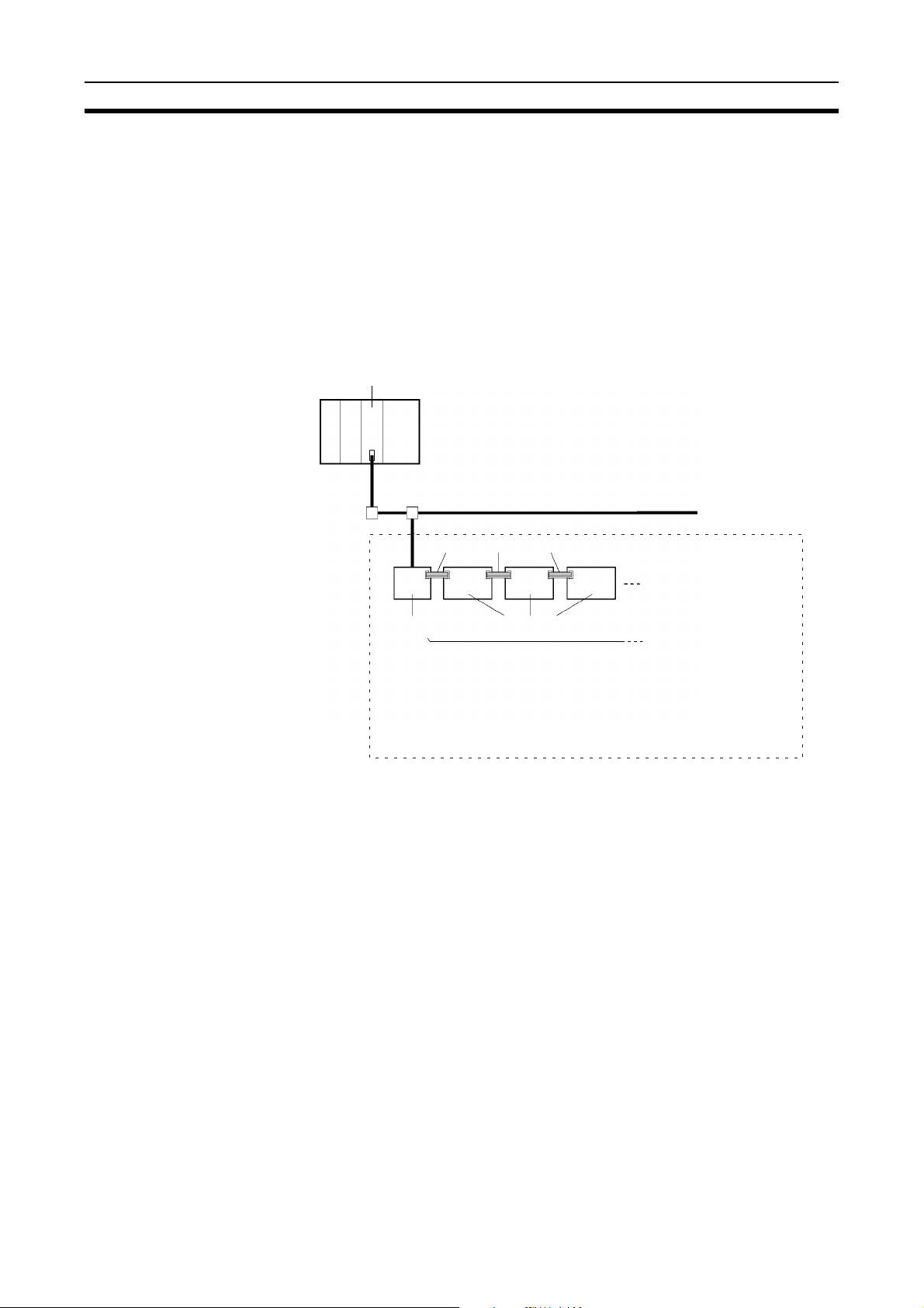
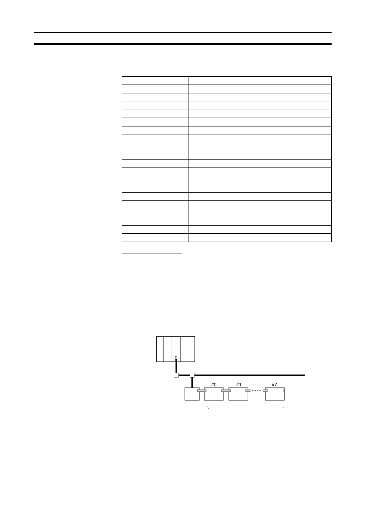
A MULTIPLE I/O TERMINAL is a building-block DeviceNet Slave that consists
of a Communications Unit tha t interfaces one o r more I/O Uni ts. The I/O Uni t
interface supports up to 8 I/O Unit s and a total of up to 1,024 I/O poi nts. I/O
Units are connected using simple s nap-on c onnectio ns via I /O Unit Con necting Cables. Allocation and addres s settings on the I/O Unit interface are not
required, enabling simple, flexible distributed I/O control.
1-1-2 System Configuration
DeviceNet Master Unit
DeviceNet Network
I/O Unit Connecting Cable
Communications
Unit
I/O Unit interface
Maximum of 8 Units; total length: 3 m, 1 m max. between Units
Total number of points (inputs + outputs): 1,024 points
The total number of points must be within the maximum number
supported by the Master.
Example: With C200HW-DRM21-V1 Master, 512 inputs/512 outputs
I/O Units
2
Page 16

MULTIPLE I/O TERMINAL Section 1-1
1-1-3 Features
Simple Connections The Communications Unit and the I/O Units are separate, and the Communi-
cations Unit and the I/O Units ar e con nected by an I/O U nit in terface. I/O can
be expanded simply by connecting additio nal I/O Units to the I/O Unit interface.
Automatic Recognition of
I/O Units
Status Notification Status information about the I/O Unit i nter face can be transm itt ed as inp uts to
Many T ypes of I/O Unit The following I/O Units are available.
An I/O-intensive System
Can be Built at Low Cost
Range Setting by
Configurator
When the power to the Communications Uni t is tur ne d ON, the models of the
I/O Units on the I/O Unit interface are aut oma tic al ly re co gni zed, and the number of remote I/O communication s points with the DeviceNet Master Unit is
automatically determined. This enables I/O to be increased or decreased simply by connecting or disconnecting I/O Units.
the DeviceNet Master Unit (two words).
• 16- or 32-point Transistor Input Units (terminal block, connector, 25-pin Dsub connector, or high-density connector)
• 16- or 32-po int Transist or Output Units (ter minal block, connector, 25-pin
D-sub connector, or high-density connector)
• 8-point/16-point Relay Output Unit (16-point Unit)
• 4- or 8-point Analog Input Unit (terminal block or connector)
• 4-point Analog Output Unit (terminal block or connector)
• 1-point Pulse Input Unit (high-speed counter)
• 4-point Temperature Input Unit
Compared with fixed I/O Terminals, a high cost-performance ratio can be
achieved if I/O Units are used.
The input and out put ranges for the Analog In put, Analog Output, an d Temperature Input Units can be set for each point using the Configurator (with version 1.11 or later). Usin g DIP switches, ranges can be set in 2-point units for
the Analog Input and Analog Output Units, and in 4-point units for the Temperature Input Unit.
3
Page 17
MULTIPLE I/O TERMINAL Section 1-1
1-1-4 Communications Units and I/O Units
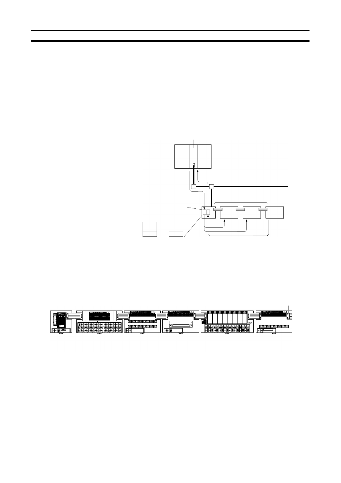
Communications Unit The Communications Unit interfaces the I/O Units to the DeviceNet.
• It controls the I/O Units in response to I/O refresh requests from the
DeviceNet Master.
• It automa tical ly rec ogni zes the configuration of the I/O Uni ts wh en th e I/O
Unit interface is initialized.
• It notifie s the con nection stat us or the s tatus informa tion for the I/O Units
to the DeviceNet Master Unit.
• It provides a DIP switch to set the node number and baud rate of the
MULTIPLE I/O TERMINAL as a DeviceNet Slave.
DeviceNet Master Unit
DeviceNet Network
I/O Unit interface
Output area
(Master → Communications Unit)
0
1
Input area
(Communications
Unit → Master)
Status
2
0
Example:
Outputs
1
Example:
Outputs
2
Example:
Inputs
I/O Units There are various I/O Units that can be connected to the I/O Unit interface.
• I/O Units are connected to the Communications Unit using an I/O Unit
Connecting Cable (included with th e I/O Unit, a 1-m I/O Unit Connecting
Cable (GCN1-100) is also available).
• No address or baud rate settings are required.
• The connection order of I/O Units is flexible.
Units with Connectors
Communications Unit
Units with Terminal Blocks
Transistor Input Unit
Transistor Output Unit
I/O Unit Connecting Cables
Included with Unit: 40 mm
GCN1-100: 1 m (sold separately)
Transistor Input Unit
Transistor Output Unit
Units with High-density
Connectors
Transistor Input Unit
Transistor Output Unit
Relay Output Unit
End connector
Analog Input Unit
Analog Output Unit
4
Page 18
MULTIPLE I/O TERMINAL Section 1-1
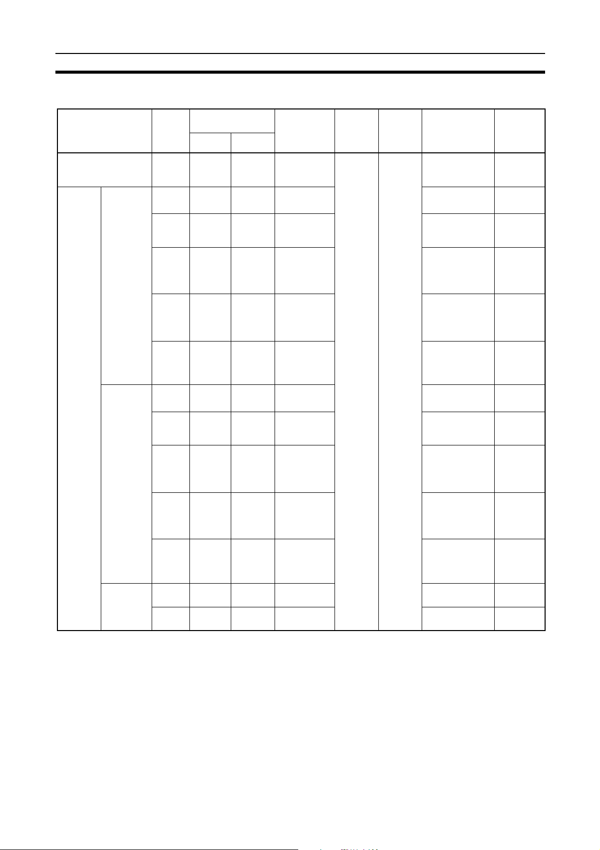
1-1-5 List of Models
Unit I/O
points
Communications Unit None Status
Basic I/O
Units
Transistor
Input Units
Transistor
Output
Units
Relay Output Units
16
inputs
16
inputs
16
inputs
16
inputs
32
inputs
16 outputs
16 outputs
16 outputs
16 outputs
32 outputs
8 outputs
16 outputs
Words allocated
in PC memory
Input Output
two
words
1 word 0 words M3 terminal
1 word 0 words Connectors
1 word 0 words Connectors
1 word 0 words Connectors
2 words 0 words High-density
0 words 1 word M3 terminal
0 words 1 word Connectors
0 words 1 word Connectors
0 words 1 word Connectors
0 words 2 words High-density
0 words 1 word M3 terminal
0 words 1 word M3 terminal
I/O
connections
0 words None 24 VDC
block
(made by
MOLEX)
(made by
FUJITSU)
(25-pin Dsub connectors)
connector
(made by
FUJITSU)
block
(made by
MOLEX)
(made by
FUJITSU)
(25-pin Dsub connectors)
connector
(made by
FUJITSU)
block
block
Unit
power
supply
voltage
(supplied
from outside)
Installa-
tion
DIN track DRT1-COM ---
Model number Remarks
GT1-ID16
GT1-ID16-1
GT1-ID16MX
GT1-ID16MX-1
GT1-ID16ML
(See note 2.)
GT1-ID16ML-1
(See note 2.)
GT1-ID16DS
(See note 2.)
GT1-ID16DS-1
(See note 2.)
GT1-ID32ML
GT1-ID32ML-1
GT1-OD16
GT1-OD16-1
GT1-OD16MX
GT1-OD16MX-1
GT1-OD16ML
(See note 2.)
GT1-OD16ML-1
(See note 2.)
GT1-OD16DS
(See note 2.)
GT1-OD16DS-1
(See note 2.)
GT1-OD32ML
GT1-OD32ML-1
GT1-ROP08 ---
GT1-ROS16 ---
NPN
PNP
NPN
PNP
NPN
PNP
NPN
PNP
NPN
PNP
NPN
PNP
NPN
PNP
NPN
PNP
NPN
PNP
NPN
PNP
5
Page 19
MULTIPLE I/O TERMINAL Section 1-1
Special I/
O Units
(See
note.)
Unit I/O
Analog
Input Units
Analog
Output
Units
Temperature Input
Units
Counter
Unit
points
4 inputs 4 words 0 word M3 terminal
8 inputs 8 words 0 word Connectors
4 outputs
4 outputs
4 inputs 4 words
1 input 3 words 3 words M3 terminal
Words allocated
in PC memory
Input Output
0 words 4 words M3 terminal
0 words 4 words Connectors
0 words M3 terminal
(8 words
depending on
mode)
I/O
connections
block
(made by
MOLEX)
block
(made by
MOLEX)
block
block
Unit
power
supply
voltage
24 VDC
(supplied
from outside)
Installa-
tion
DIN track GT1-AD04
Model number Remarks
(See note 2.)
GT1-AD08MX
GT1-DA04
(See note 2.)
GT1-DA04MX Outputs:
GT1-TS04T Inputs:
GT1-TS04P Inputs:
GT1-CT01 1 external
Inputs:
4 to
20 mA, 0
to 20 mA,
0 to 5 V,
1 to 5 V,
0 to 10 V,
–10 to
10 V
Outputs:
4 to
20 mA,
0 to 5 V,
1 to 5 V,
0 to 10 V,
–10 to
10 V
0 to 5 V,
1 to 5 V,
0 to 10 V,
–10 to
10 V
R, S, K, J,
T, B, L
Pt100,
JPt100
input
2 external
outputs
Note The front-panel indic ators and o ther parts of An alog Input Units, Analog O ut-
put Units, Temperature Input Units, and Counter Units differ from those of
other I/O Units. These Units belong to a group called Special I/O Units.
An end connector is attache d to the Communications Unit, and a 40-mm I/O
Unit Connecting Cable is included with each I/O Unit. A 1-m I/O Unit Connecting Cable (GCN1-100) is also available.
1 m
6
Page 20

MULTIPLE I/O TERMINAL Section 1-1
Applicable Connectors The applicable connectors are shown in the following table.
Connector Model number Remarks
Connectors made
by MOLEX
Connectors made
by
FUJITSU
corresponding to 16point connectors
Recommended
connectors
corresponding to 25pin D-sub
connectors
Connectors made
by
FUJITSU
corresponding to highdensity
connectors
Pressurewelded
Crimp Housing 51030-0330
Soldered FCN361J024-AU
Pressure-welded FCN367J024-AU/F
Crimp FCN363J024-AU
Hood XW2S-2513 OMRON
Plug XW2A-2501 OMRON
Soldered FCN361J040-AU
Pressure-welded FCN367J040-AU/F
Crimp FCN363J040-AU
Housing 52109-0390 For AWG#24
(See note.)
Reeled contacts
Loose contacts
Crimping tool 57036-5000 For AWG#22 to 26
50083-8014 For AWG#24 to 30
50084-8014 For AWG#22 to 24
50083-8114
(See note.)
50084-8114 For AWG#22 to 24
57037-5000
(See note.)
For AWG#24 to 30
For AWG#24 to 30
Note Refer to page 219, High-de ns ity Conn ector Cables for MULTIP LE I/ O TE RMI-
NALs for detai ls.
7
Page 21

Functions Section 1-2
1-2 Functions
1-2-1 I/O Unit Interface Specifications
Item Specification
Communications method Special protocol
Number of I/O Units 8 Units max.
Maximum number of points Total inputs/outputs: 1,024 points (bits)
Communications dis-
tance
Communications power supply Supplied from the Commu nications
Relationship to DeviceNet After the I/O Unit interface is estab-
Addresses Automaticall y recogn ized when the
I/O configuration Automaticall y rec ogn ized when the
Self-diagnostic functions
Error detection Frame error ch eck; CRC-CCITT check
Total length 3 m max.
Between Units 1 m max. (Cable included with Unit is
Configuration errors The I/O Unit configuration is constantly
Special I/O Unit
errors
I/O Unit interface
errors
Power supply overload to I/O Units
40 mm.)
Unit to the I/O Unit (0.4 A max.)
lished, Device Net co mm unica tion s continue normally, even if an error occurs
on the I/O Unit interface.
power to the Communi ca tio ns Unit is
turned ON.
power to the Communi ca tio ns Unit is
turned ON. If the configuration is
changed while the pow er sup ply is ON,
a configuration error will occur.
checked while power is supplied. If a
mismatch occurs while the power is
turned ON, I/O refreshing for all I/O
Units is stopped.
Errors are detected in the Special I/O
Units (Analog Input Units, Analog Output Units, Temperature Inpu t Units , and
Counter Units) on the I/O Unit interface.
Communications stop when there is no
communications response from an I/O
Unit.
Communications stop when there is no
specific response from the la st I/O Unit
(terminator).
Communications stop when nine or
more I/O Units are connected.
The power supply to the I/O Un its an d I/
O refreshing for all I/O Units are
stopped when the power supply to the
I/O Units through the Communications
Unit exceeds 0.4 A.
8
Page 22
Functions Section 1-2
I/O Interface Current
Consumption
Make sure that the power supply from the Communications Unit to the I/O
Units is less t han the total rated output cur rent (400 mA). The I/O in terface
current consumption for each I/O Unit is shown in the following table.
I/O Unit I/O interface current consumption
GT1-ID16(-1) 35 mA max.
GT1-ID16MX(-1) 35 mA max.
GT1-ID16ML(-1) 35 mA max.
GT1-ID16DS(-1) 35 mA max.
GT1-ID32ML(-1) 55 mA max.
GT1-OD16(-1 ) 35 mA max.
GT1-OD16MX(-1) 35 mA max.
GT1-OD16ML(-1) 35 mA max.
GT1-OD16DS(-1) 35 mA max.
GT1-OD32ML(-1) 65 mA max.
GT1-ROP08 40 mA max.
GT1-ROS16 50 mA max.
GT1-AD04 50 mA max.
GT1-AD08MX 50 mA max.
GT1-DA04 50 mA max.
GT1-DA04MX 50 mA max.
GT1-TS04T 50 mA max.
GT1-TS04P 50 mA max.
GT1-CT01 90 mA max.
I/O Unit Interface
Addresses
Calculation Example
When five GT1-ID32ML Input Units and three GT1-OD16 Output Units are
used, the total current consumption is calculated as follows:
(GT1-ID32ML current consumption) x 5 Units
+ (GT1-OD16 current consumption) x 3 Units
= 55 mA x 5 + 35 mA x 3 = 380 mA
≤ 400 mA
The addresses of the I/O U nits on the I/O Unit interface are automati cally se t
when the Communications Unit is started. The addres ses are from 0 to 7 in
ascending order from the I/O Units closest to the Communications Unit.
DeviceNet Master Unit
DeviceNet Network
I/O Unit interface
Communications Unit
I/O Unit I/O Unit I/O Unit
Checking the I/O Unit
Interface Status
The following two methods are used to check the I/O Unit interface status:
• Checking the Communications Unit and I/O Unit indicators
• Checking the status of the Communications Unit
9
Page 23
Functions Section 1-2
Indicators
DeviceNet
Network
Communications Unit
TS indicator
I/O Unit I/O Unit
Unit Normal Error
Communications
Unit
TS Indicator:
Lit green
TS indicator
I/O Unit interface error: Lit red
Special I/O Unit error: Flashing green
Maximum power supply
overload to I/O Units: Not lit
I/O Units TS indicator:
Lit green
U.ERR indica-
tor: Not lit
PWR indicator:
Lit green
TS indicator
I/O Unit interface error: Lit red
U.ERR indicator
Special I/O Unit error: Lit red
PWR indicator
No internal power supply: Not lit
For details, refer to page 199, Troubleshooting via Indicators.
Checking the I/O Unit Interface Status
The first two words of the CPU Unit all ocatio n in put area are always allocated
to the status of the I/O Unit interface via the DeviceNet.
DeviceNet Master Unit
Communications Unit
Output
Input
area
area
DeviceNet Network
I/O Unit I/O Unit
Status, two words
0 wd
I/O Unit connection information
Error slaves Registered slaves
+1 wd
For details, see page 15.
1-2-2 Ex changing Data
Initialization When the Communications Unit is started, it automatically recognizes the
configuration of the I/O Units and registers this status as the n ormal co nfiguration (in RAM memor y). At the same time, addr esses 0 to 7 are alloca ted to
the I/O Units in ascend ing order from the I/O Unit c losest to the Communications Unit. The se pr ocesses are performed ea ch t im e th e p ower is turned ON.
10
Page 24

Functions Section 1-2
Remote I/O communications with the DeviceNet Master Uni t are carried out
by a MULTIPLE I/O TERMINAL base d on the registered co nfiguration. Whe n
the power to the Communications Unit is turned ON, the bits allocated to the I/
O Units can be used to check the status (bits 0 to 7 of the first word) of the
Communications Unit.
DeviceNet Network
Communications Unit
At startup
I/O Unit I/O Unit I/O Unit
Automatically recognizes the configuration of the
I/O Units
Communications with the DeviceNet Master Unit
based on this I/O configuration
Note 1. If the configuration of the I/O Units is to be changed, a number of pr ecau-
tions must be noted. For details, see 1-2-5 I/O Configuration Changes.
2. For details of data exchange timing, see 6-1-1 I/O Response Time.
Error Processing Even if an error occurs in the I/O Unit interface after initialization is completed,
DeviceNet communications will continue normally. Therefore, an error processing program section must be included in the CPU Unit to check the status
of the Communications Unit for errors that have occurred and to identify the
error type and location.
1-2-3 Allocating I/O
This section explains how words for a MULTIPLE I/O TERMINAL are allocated in the output area and input area of the Master. For details of remote I/O
functions in the output area and input area of the Master such as word specification, fixed allocation, and user-set al loca tio n, refer to the DeviceNet Opera-
tion Manual (W267).
Fixed Allocation The output area and i nput area corresponding to the Communica tions Unit
node number for a MULTIP LE I/O TERMINAL are as shown in the following
diagram.
Output Area
The output area contains outp ut bits in the orde r that I/O Units are co nnecte d
on the I/O Unit interface.
Input Area
The input area contains the Communications Unit status (two words), and
input bits in the order that I/O Units are connected on the I/O Unit interface.
Output area Input area
Area corresponding to
Communications Unit
node number
Output bits on
the I/O Unit
interface
I/O Unit interface
status
Input bits on the I/O
Unit interface
The input and output bits for the I/O Unit interface are allocated in the
DeviceNet input and output a reas in 16-p oint (one word) increments. With 8point I/O Units, these bits are alloc ated using the r ightmost byte (bits 0 to 7) ,
and the leftmost byte (bits 8 to 15) will be 00 Hex.
11
Page 25
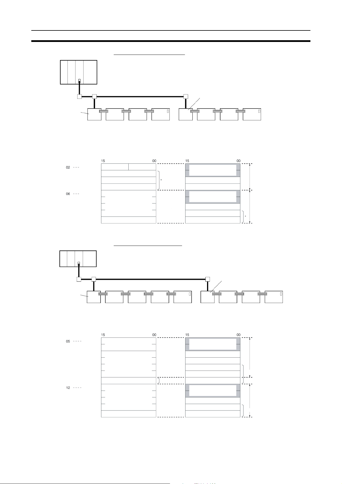
Functions Section 1-2
Example: CVM1/CV Series
Communications Unit
node number 02
I/O Unit
addresses
Communications Unit
node number
CIO 1902
CIO 1903
CIO 1904
CIO 1905
CIO 1906
CIO 1907
CIO 1908
CIO 1909
CIO 1910
DeviceNet Network
#0
16 inputs#18 outputs#216 inputs
Output area Input area
00 Hex
8 output bits for
Unit #1
Unused
Unused
Unused
CIO 2002
CIO 2003
CIO 2004
CIO 2005
16 input bits for Unit #0
16 input bits for Unit #2
CIO 2006
4 analog
outputs for
Unit #1
CIO 2007
CIO 2008
16 input bits for Unit #0
CIO 2009
16 output bits for Unit #2
CIO 2010
The unused words can be used as work bits.
Example: C200HX/HG/HE
Communications Unit
node number 06
#0
16 inputs
I/O Unit interface status
for node number 02
I/O Unit interface status
for node number 06
#1
4-point
Analog
Output
Unit
Unused
Unused
#2
16 outputs
Area allocated to
Communications Unit
for node number 02
Area allocated to
Communications Unit
for node number 06
Communications Unit
node number 05
I/O Unit
addresses
Communications Unit
node number
DeviceNet Network
#0
32 outputs
#1
4-point
Analog
Output Unit
#2
16 inputs
#3
16 inputs
Communications Unit
node number 12
#0
16 inputs#14-point
Analog
Output Unit
Output area Input area
(See
note 1.)
CIO 355
CIO 356
CIO 357
CIO 358
CIO 359
CIO 360
CIO 361
CIO 362
CIO 363
CIO 364
CIO 365
CIO 366
I/O Unit interface status
for node number 05
16 input bits for Unit #2
16 input bits for Unit #3
Unused
Unused
Unused
I/O Unit interface status
for node number 12
16 input bits for Unit #0
Unused
Unused
Area allocated to
Communications Unit
for node number 05
(See note 1.)
Area allocated to
Communications Unit
for node number 12
(See note 2.)
CIO 55
CIO 56
CIO 57
CIO 58
CIO 59
CIO 60
CIO 61
CIO 62
CIO 63
CIO 64
CIO 65
CIO 66
32 output bits for
Unit #0
4 analog outputs
for Unit #1
Unused
4 analog outputs
for Unit #1
16 output bits for Unit #2
Note 1. The unused words between I/O areas that are used cannot be used as work bits.
2. The unused words (not between I/O areas that are used) can be used as work bits.
#2
32 outputs
12
Page 26

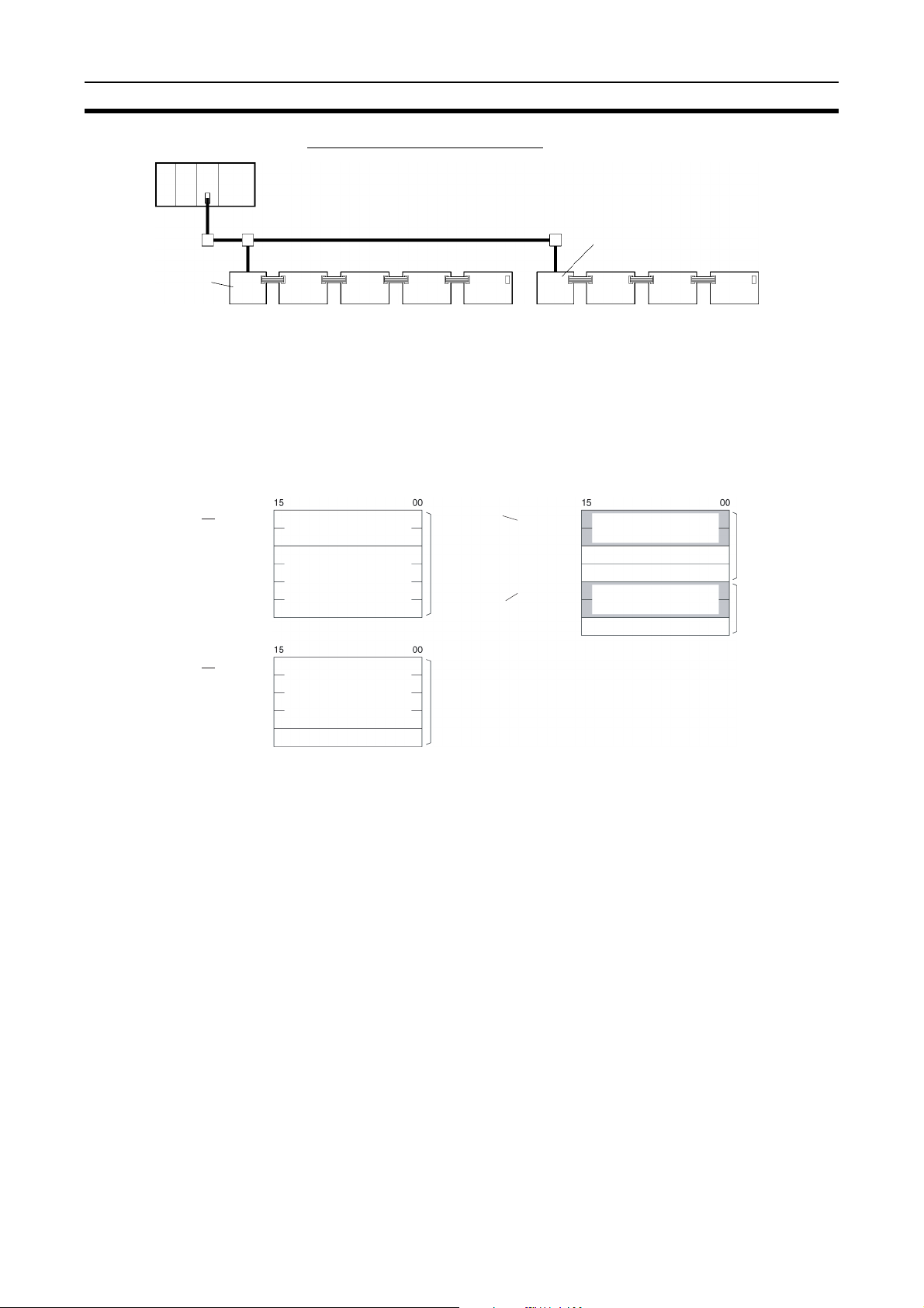
Functions Section 1-2
User-set Allocation The Configurator can be used to set the Communi cations Unit node number,
first word, and number of bytes to all ocate (allocation size) for input block 1
and 2 and for output block 1 and 2, as shown in the following diagram.
Output block 1 or 2: Output bits in the order I/O Units are connected on
the I/O Unit interface
Input block 1 or 2: I/O Unit interface status (two words), and input bits in
the order I/O Units are connected on the I/O Unit
interface
Communications Unit
node number 02
I/O Unit
addresses
Allocation settings for node number 02
First word: CIO 1952
Allocation size: 2 bytes (1 word)
Allocation settings for node number 06
First word: CIO 1954
Allocation size: 10 bytes (5 words)
Output block 1 or 2
First word
Output bits on the
I/O Unit interface
Example: CVM1/CV Series
DeviceNet Network
#0
16 inputs
#1
8 outputs
# 2
16 inputs
Input block 1 or 2
First word
Allocation size
Communications Unit
node number 06
#0
16 inputs
Allocation settings for node number 02
First word: CIO 1904
Allocation size: 8 bytes (4 words)
Allocation settings for node number 06
First word: CIO 1901
Allocation size: 6 bytes (3 words)
I/O Unit interface
status
Input bits on the
I/O Unit interface
#1
4-point
Analog
Output Unit
#2
16 outputs
Allocation size
First word
of node
number 02
First word
of node
number 06
CIO 1950
CIO 1951
CIO 1952
CIO 1953
CIO 1954
CIO 1955
CIO 1956
CIO 1957
CIO 1958
Output block 2
00 Hex
4 analog outputs
for Unit #1
16 input bits for Unit #2
8output bits for
Unit #1
First word
of node
number 06
Size of node
number 02
First word
of node
number 02
Size of node
number 06
CIO 1900
CIO 1901
CIO 1902
CIO 1903
CIO 1904
CIO 1905
CIO 1906
CIO 1907
Input block 1
I/O Unit interface status
for node number 06
16 input bits for Unit #0
I/O Unit interface status
for node number 02
16 input bits for Unit #0
16 input bits for Unit #2
Size of node
number 06
Size of node
number 02
13
Page 27
Functions Section 1-2
Example: C200HX/HG/HE Series
Communications Unit
node number 05
I/O Unit
addresses
First word
of node
number 05
First word
of node
number 12
DeviceNet Network
#0
32 outputs
Allocation settings for node number 05
First word: CIO 50
Allocation size: 12 bytes (6 words)
Allocation settings for node number 12
First word: CIO 120
Allocation size: 10 bytes (5 words)
CIO 50
CIO 51
CIO 52
CIO 53
CIO 54
CIO 55
CIO 120
CIO 121
CIO 122
CIO 123
CIO 124
32 output bits for
Unit #0
16 output bits for Unit #2
#1
4-point
Analog
Output Unit
Output block 1
4 analog outputs
for Unit #1
Output block 2
4 analog outputs
for Unit #1
#2
16 outputs
# 3
16 inputs
First word
of node
number 05
Size of node
number 05
First word
of node
number 12
Size of node
number 12
Communications Unit
node number 12
#0
16 outputs
Allocation settings for node number 05
First word: CIO 360
Allocation size: 3 bytes (4 words)
Allocation settings for node number 12
First word: CIO 363
Allocation size: 8 bytes (3 words)
CIO 360
CIO 361
CIO 362
CIO 362
CIO 363
CIO 364
CIO 365
16 input bits for Unit #2
16 input bits for Unit #3
16 input bits for Unit #0
#1
4-point
Analog
Output Unit
Input block 1
I/O Unit interface status
for node number 05
I/O Unit interface status
for node number 12
#2
16 outputs
Size of node
number 05
Size of node
number 12
14
Page 28

Functions Section 1-2
Allocation Precautions Note the following precautions when starting the DeviceNet Network.
Limits on the Total Number of Input and Output Points for a Master Unit
A maximum of 1,024 in puts and outpu ts can be c ontrolled by one Com munications Unit (DRT1-COM). The number of I/O points for each node, however,
depends on the Master Unit. For example, with the CV-series Master Unit
(CVM1-DRM21-V1) or the C200HX/HG/HE and C200HS Master Unit
(C200HW-DRM21-V1), up to 512 inputs and up to 512 outputs can be used at
each node. Therefore, connect I/O Uni ts within a range that does not exceed
the number of I/O points for each Master Unit node. The following table shows
the I/O size of each Unit.
Unit model Number of
inputs
DRT1-COM 32 points 0 point
GT1-ID16(-1), GT1-ID16MX(-1), GT1-ID16ML(-1)*,
GT1-ID16DS(-1)*
GT1-OD16(-1), GT1-OD16MX(-1), GT1-OD16ML(-1)*,
GT1-OD16DS(-1)*, GT1-ROS16, GT1-ROP08
GT1-ID32ML(-1) 32 points 0 point
GT1-OD32ML(-1) 0 points 32 points
GT1-AD04* 64 points 0 points
GT1-AD08MX (With 8-input mode) 128 points 0 points
GT1-AD08MX (With 4-input mode) 64 points 0 points
GT1-DA04*, GT1-DA04MX 0 points 64 points
GT1-TS04T, GT1-TS04P (With Normal Mode) 64 points 0 points
GT1-TS04T, GT1-TS04P (With 2-decimal-place Mode) 128 points 0 points
GT1-CT01 48 points 48 points
16 points 0 point
0 points 16 points
Number of
outputs
The GT1-ROP08 (Relay Output Unit with Power Relay) has 8 actual outputs
but, as a MULTIPL E I/O TERMINAL, the number of outputs allocated to the
Master Unit is 16.
Calculation Example
When one GT1-DA04MX Analog Output Unit and three GT1-AD08 Analog
Input Units are used, th e tot al num ber of inp u t p oin ts and outp ut p oin ts is calculated as follows:
Total Number of Input Points:
Communications Unit (Status) + Analog Input Units x 3
= 32 points + 128 points x 3 = 416 points
Total Number of Output Points:
Analog Output Units x 1
= 64 points
Reference
For information on dealing with oth er problems c onc erning the MULTIPLE I/O
TERMINAL, refer to SECTION 7 Troubleshooting and Maintenance. For information on problems concer ning the DeviceNet, refer to DeviceNet Operation
Manual (W267).
1-2-4 I/O Unit Interface Status
The following I/O Unit interface status is maintained in the CPU Unit.
• I/O Unit connection information (I/O Unit interface status)
• Registered I/O Unit addresses
15
Page 29

Functions Section 1-2
• Error I/O Unit addresses
As shown in the following diagram, the status consists of two words. The first
two words of the Communic ations Unit alloc ation input are a in the CPU Uni t
are allocated for this status. Include a program section in the CPU Unit to
check this status and perform error processing.
I/O Unit Connection Information
0 wd
1: Error (OR of bits 0 to 4)
1: Refreshing I/O
Bit Flag name Meaning Content
15 Refreshing I/O Refreshing I/O 1: Communications between the
14 Error OR of bits 0 to 4 1: Any one of bits 0 to 4 is ON
4 High-density
I/O Unit Error
3 I/O Unit Pow er
Supply Overload
2 I/O Unit Inter-
face Error
1 Configuration
Error
0 Special I/O
Unit Error
0 wd
+1 wd
A high-density I/O Un it error w as
detected.
An overcurrent to an I/O Unit
was detected.
An I/O Unit interface error was
detected.
Data Transfer Error:
In the I/O Unit interfa ce, there
was no response to a command after the fixed time has
elapsed. Alternatively, the
response expected to be
returned from the end I/O Unit
(terminator) was not received.
Too many I /O Units:
Nine or more I/O Units are
connected.
The I/O con figuration was
changed when the Communications Unit was started.
An error occurred in a Special
I/O Unit.
Error I/O Unit addresses Registered I/O Unit addresses
I/O Unit connection information
Bit
1: Special I/O Unit Error
1: Configuration Error
1: I/O Unit Interface Error
1: I/O Unit Power Supply Overload
1: High-density I/O Unit Error
Communications Unit and I/O Units
is normal.
0: Communications error (no
response is received from an I/O
Unit)
0: Bits 0 to 4 are all OFF
1: Unit error
0: Unit normal
1: Overcurrent detected
0: Normal
1: I/O Unit interface error
0: Normal
1: I/O configuration change during
startup
0: No I/O configuration change during
startup
1: Special I/O Unit error
0: Special I/O Unit normal
16
Page 30

Functions Section 1-2
Abnormal I/O Unit Addresses and Registered I/O Unit Addresses
Bit
+1 wd
1-2-5 I/O Configuration Changes
The I/O Unit interface automatically recognizes the I/O Unit configuration each
time the Communications Unit is star ted up, and stores this as the normal
configuration.
Note 1. If the I/O Unit configuration is c hanged wh ile the Communications Unit is
turned ON, a configuration error will occur. Do not change the I/O Unit configuration while power is being supplied to the Communications Unit.
2. If a configuration error occurs on the I/O Unit interface, I/O refreshing of all
I/O Units will stop. Even if a configuration er ror occurs, communications
with the DeviceNet Network will continue, using the initial I/O Unit configuration. An error processi ng p rogram se cti on mus t the re fore be includ ed i n
the CPU Unit to regular ly check whether or not a configuratio n error has
occurred (status bit 1) and to process abnormal I/O Unit addresses.
If the I/O Unit configuration is changed, perform the following operations,
according to the DeviceNet area al loc at ion meth od. For details abou t I/O all ocation, refer to DeviceNet Operation Manual (W267).
The bits corresponding
to I/O Unit with errors
are turned ON. Bits 8 to
15 correspond to
addresses 0 to 7.
1: Error
0: No error, or not
part of network
The bits corresponding
to registered I/O Units
are turned ON. Bits 0 to
7 correspond to
addresses 0 to 7.
1: Registered
0: Not registered
Default Allocations Because the allocation size of the Communications Unit changes together
with changes to th e I/O Unit configuration, a verification er ror will occur on
DeviceNet if the scan list is enabled, as follows:
• Master Unit 7-segment display will show d6, Slave I/O size mismatch.
• Master status bits 14 and 7 will turn ON.
Perform the following operations, according to the status of the input/output
areas.
Allocation Areas Do Not Overlap with Other Slaves
Remote I/O communication s will be performed unchanged wi th the new configurat io n. C heck the V erif ic at i o n Error Bit and, if require d, pe r form processing
to disable the allocated words in the CPU Unit. Also check the number of
points for the changed I/O Unit and its allocation ar ea on the I/O Unit interface, and re-register the scan list (first set the Scan List Enable software
switch to OFF, and then set it to ON after checking the I/O size).
Allocation Areas Overlap with Other Slaves
In this case, I/O area duplication will also occur on the DeviceNet, as follows:
• Master Unit 7-segment display will show d0, I/O area duplication.
• Master status bits 14 and 4 will turn ON.
Check the Verification Error Bit, and per form processing to disable the allocated words in the CPU Unit. Also ch ang e the S lave node number so that th e
allocation area doe s not overlap with any other, and re-register the sca n list
(first set the Scan Lis t Enable software switch to OFF, and then set it to ON
after checking the I/O size).
Note If the scan list is disabled, there will be no changes made in the DeviceNet
Master Unit, even if the Communication s Unit input/output sizes ch ange. Be
sure to use the Scan List Enable Mode for normal operations.
17
Page 31

Functions Section 1-2
User-set Allocations The sizes of the allocated areas for the Communications Unit will change with
changes to the I/O Un it con figuration , ca using a Verification Error to occur o n
DeviceNet if the scan list is enabled, as follows:
• Master Unit 7-segment display will show d6, a Slave I/O size mismatch.
• Master status bits 14 and 7 will turn ON.
Perform the following operations, according to the status of the input/output
areas.
Allocation Areas Do Not Overlap with Other Slaves
Remote I/O communication s will be performed unchanged wi th the new configuration data. Check the Verification Error Bit and , if required, perform processing to disable the allocated words in the CPU Unit. A lso, perform change
the allocations using the Configurator.
Allocation Areas Not Overlap with Other Slaves
In this case, I/O area duplication will also occur on the DeviceNet, as follows:
• Master Unit 7-segment display will show d0, I/O area duplication.
• Master status bits 14 and 4 will turn ON.
Check the Verification Error Bit, and per form processing to disable the allocated words in the CPU Unit. Also, perform change allocations using the Configurator.
18
Page 32

Hardware Setup and Operational Check
This section provides the basic procedure for operation and includes an actual example.
2-1 Basic Procedure . . . . . . . . . . . . . . . . . . . . . . . . . . . . . . . . . . . . . . . . . . . . . . . 20
2-2 Specific Example . . . . . . . . . . . . . . . . . . . . . . . . . . . . . . . . . . . . . . . . . . . . . . 21
SECTION 2
19
Page 33

Basic Procedure Section 2-1
2-1 Basic Procedure
The basic operating procedure is shown below. For details about settings and
connections, re fer to DeviceNet Operation Manual (W267). For explanations
about Slave Units, refer to SECTION 4 Basic I/O Unit Specifications and SEC-
TION 5 Special I/O Unit Specifications.
Inputs: Number of points/input type/connection type
1
Determine the MULTIPLE
I/O TERMINAL I/O
specifications.
Outputs: Number of points/input type/connection type
Analog inputs: Number of points
Analog outputs: Number of points
Temperature inputs: Number of points
Pulse inputs (counter): Number of points
2
Select the I/O Units.
3
Check the specifications.
4
Mount and connect the
Communications Unit and
I/O Units.
Set the DIP switches for the
5
Communications Unit,
Analog Input Units, Analog
Output Units, and
Temperature Input Units.
6
Connect to the DeviceNet
Master Unit.
Communications
Unit (1)
+
Transistor Input
Terminal
Connec-
block
tor
16 points 16 points 32 points 16 points 16 points 32 points 16 points 8 points 4 points8 points
Unit
Unit Unit Unit Unit Unit Unit Unit Unit Unit
High-density connector
+
Terminal
block
Transistor Output
Connec-
High-den-
tor
sity connector
Relay Output Analog
Terminal
block
+
Input Output
Analog
Counter
Input
1 points
Unit
The combined total of input points and output points for each Communications Unit is 1,024 max.
The total current supplied from the Communications Unit to each I/O Unit (I/O Unit interface current
consumption) is 0.4 A max.
Mount Units on DIN track (DIN 35-mm track: all Units).
Connect I/O Unit Connecting Cabled and end connector.
Connect Communications Unit internal power supply (24 VDC −15%/+10%).
Connect I/O power supply (24 VDC −15%/+10%) for each Transistor Input/Output Unit and Relay
Output Unit.
Connect I/O power supply (24 VDC −15%/+10%) for each Analog Input/Output Unit and
Temperature Input Unit, as well as power supply for each Counter Unit encoder, using a separate
power supply from the above.
Connect I/O to each I/O Unit.
Set the node number of the Communications Unit as a DeviceNet Slave, and the hold/clear output
settings for the baud rate and communications errors.
Set the Analog Input Unit, Analog Output Unit, and Temperature Input Unit ranges and other
specifications. (When setting the Analog Input Unit, Analog Output Unit, and Temperature Input
Unit ranges from the Configurator, set the DIP switch to Software Setting Enable.)
Connect the Communications Unit to the DeviceNet Master Unit using the DeviceNet
Communications Cable.
7
Turn ON the power.
8
Set using the Configurator.
9
Set the Scan List Enable
switch.
10
Check the operation.
20
Turn ON the PC power supply.
Turn ON the DeviceNet communications power supply.
Turn ON the Communications Unit internal power supply.
Turn ON the I/O power supply to individual I/O Units.
Set as required for the Communications Unit, Analog Input Units, Analog Output Units, and
Temperature Input Units using the DeviceNet Configurator (versions 1.11 and later).
Set to enable the DeviceNet Master Unit scan list (from a PC Peripheral Device or
the Configurator).
Check the I/O Unit interface status.
Check the indicators on all Units.
The following indications are normal:
Communications Unit MS indicator: Lit green
Communications Unit NS indicator: Lit green
TS indicators for I/O Units: Lit green
Check that the data for the I/O words allocated in the I/O memory (with default allocations, in the
DeviceNet area) of the CPU Unit of the PC is being correctly read and written by the CPU Unit.
Page 34

Specific Example Section 2-2
2-2 Specific Example
1,2,3... 1. Determine the MULTIPLE I/O TERMINAL I/O specifications.
Each Communications Unit for the MUL TIPLE I/O TERMINAL can be connected to a combined total of 1,024 input and output points (64 words)
max. (This figure does not incl ude the 2 words of the inp ut area all ocate d
to the I/O Unit interface status.)
In this example, the following configuration will be used:
• Inputs: 16 points
• Outputs : 16 points
• Analog Input: 8 inputs (8 words)
• Analog Output: 4 outputs(4 words)
2. Select the I/O Units.
• DRT1-COM Communications Unit: 1 Unit
• GT1-ID16 Transistor Input Unit, 16 points with terminal block: 1 Unit
• GT1-OD16MX Transistor Output Unit, 16 points with connector:1 Unit
• GT1-AD08MX Analog Input Unit, 8 inputs: 1 Unit
• GT1-DA04MX Analog Output Unit: 4 outputs: 1 Unit
3. Check the specifications.
• Check that the total number of input and output po in ts (words) is less
than 1,024 (64). In this example, the number of points is calculated as
follows:
Inputs (16 poin ts) + O utp uts (16 points) + Anal og Inp ut (8 wor ds x 1 6
points) + Analog Output (4 words x 16 points)
= 224 points
Note There are DeviceNet Master Units that have restrictions on the num-
ber of input and output points per Slave Unit. Make sure that the
number of input and output point s does not exceed the limit for the
Master Unit. (For example, the C200 HW-DRM21-V1 has an upper
limit of 512 for both input and output points.) The maximum number
of input and output points for the Master Unit, includ es the 2 words
allocated to the I/O Unit i nterface status. When calcula ting the total
number of input and output points, be sure to include this (32 points)
in the calculation.
• Check that the total I/O Unit interface current consumption is less than
0.4 A. In this example, the total is calculated as follows:
Transistor Input Unit (35 mA) + Transistor Output Unit (35 mA) + Analog Input Unit (50 mA) + Analog Output Unit (50mA)
=170 mA
4. Mount and connect the Communications Unit and I/O Units.
• Mounting on the DIN Track
Communications
Unit
Transistor Input Unit:
with terminal block
Transistor Input Unit
with connector
Analog Input Unit
Analog Output Unit
DIN track
21
Page 35

Specific Example Section 2-2
• Connecting I/O Unit Connecting Cable
GT1-ID16
GT1-OD16MX
I/O Unit Connecting Cable
Standard cable: 40 mm
GCN1-100: 1 m
(One cable is included with
each I/O Unit.)
GT1-AD08MX
Same I/O Unit Connecting
Cable as at left
End connector
(One is provided with the
Communications Unit.)
To connect each pair of Units, con nect I/ O Unit in terface communic ations
connector 2 o n the Unit cl oser t o the Co mmunica tions U nit to I/O U nit i nterface communications connector 1 on the Unit closer to the end Unit.
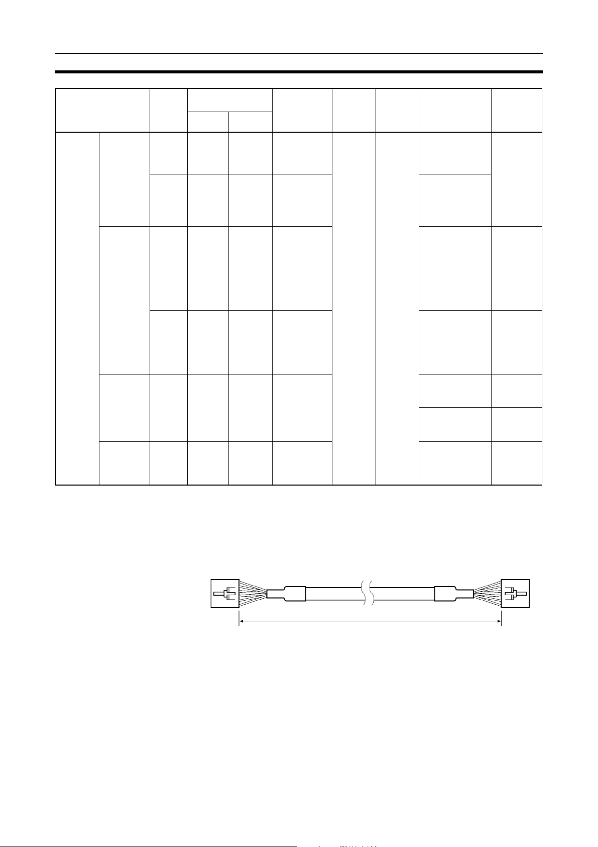
Note The connecting cable for the I/O Unit is shown below.
Accessory Cable
GT1-DA04MX
Communications
Unit
24-VDC
power supply
GCN1-100
Transistor Input Unit
with terminal block
24-VDC
power supply
40 mm
1 m
• Connecting Communications Unit and I/O Unit Power
Transistor Input Unit
with connector
Analog Input Unit Analog Output Unit
24-VDC
power supply
Note Be sure to separate the communi cations power supply, the internal
power supply for the Communications Unit and the CPU Bus Unit,
and the power supplies for the I/O Units. If the same power supply is
used, malfunction due to noise may occur.
The capacity required for the Communications Unit internal power supply,
can be obtained using the following formula:
Communications Unit internal power supply current
= Communications Unit internal current consumption + Sum of I/O Unit Interface current consumption
22
Page 36

Specific Example Section 2-2
Note T he ab ove formula appl ies when a voltage o f 2 4 VDC is su ppl ie d t o
the Commun icati ons Un it int ernal po we r suppl y terminal s. If the su pplied voltage become s lower, the current c on su mpti on wi ll in cre as e.
Select a device for the power supply that will allow a degre e of variation.
When selecting a power supply, take inrush c urrent into consideration.
The following OMRON products are recommended for the 24-V DC
power supply:
S82K-05024: 100 to 120/200 to 240 VAC, 50 W
S82K-10024: 100 to 120/200 to 240 VAC, 100 W
S82J-5524: 100 to 120 VAC, 50 W
S82J-5024: 100 to 120 VAC, 100 W
For details of the I/O Unit interface current consumption for the Units,
refer to page 9, I/O Interface Current Consumption.
Select power supplies for the I/O Units that are suitable for the load currents to
be used and the Units’ internal drive currents (refer to page 41).
• Connecting I/O Units to I/O
Communications
Unit
Transistor Input Unit
with terminal block,
16 points
Transistor Output Unit
with connector,
16 points
Analog Input Unit,
8 input
Analog Output Unit,
4 outputs
5. Set the DIP switches for the Communications Unit, Analog Input Unit, and
Analog Output Unit.
Communications Unit Analog Input Unit Analog Output Unit
Node
number
Baud rate
Hold/clear
outputs for
communications
errors
Input range Operating
specifications
• Averaging
• 4 or 8 inputs
• Software Setting
Enable/Disable
Output
range
Operating
specifications
• Output when an
• Software Setting
Enable/Disable
I/O Unit interface
error occurs
Note a) If a DeviceNet Configurator (versions 1.1 1 and later) is used, the
input range for Analog Input Units, the output range for Analog
Output Uni ts, and I/O Unit int erf ace error ou tput (hig h-clear ou tput/
low-clear output) can be set via the network. When setting from
the Configurator, use the DIP switch to set the Software Setting
Enable/Disable setting to Enable. For details, refer to 5-1 An alog
Input Units and 5-2 Analog Output Units.
23
Page 37

Specific Example Section 2-2
b) You must also use the DIP switch a nd the Conf igurator to s et the
Temperature Input Unit. For details, refer to 5-3 GT1-TS04T and
GT1-TS04P Temperature Input Units.
Left side of
cassette
Operating specifications
• T emperature unit
• Number of decimal places used
• Enable/disable software settings
• Input type
• Input range
6. Connect to the DeviceNet Master Unit.
Communications
power supply
24 VDC
Communications
Unit
DeviceNet Network
Temperature Input Unit
I/O Unit
7. Turn ON the power.
8. Set using the Configurator.
Using version 1.11 or later versions of the DeviceNet Configurator, it is
possible, via the network, to set the following:
• Input range for Analog Input Units.
• Output range for Analog Output Units.
• I/O Unit i nterface error output (low-clear output/hi gh-clear output) for
Analog Output Units.
Note a) When using a DIP switch, the input and output ranges for the An-
alog Input and Output Units can be set in 2-point units, whereas
with a Configurator, a setting can be made for each point.
b) You can set the Temperature Input Unit input range as well as the
I/O Unit settings us in g th e Co nfi gura tor. For details, refer to 5-3-2
Settings Using the Configurator.
9. Create the scan list.
24
Set the Scan List Enable switch (PC software switch) to ON. For example,
for a DeviceNet Master Unit with unit address 0 installed in a C200HX/HG/
Page 38

Specific Example Section 2-2
HE(-Z) PC, turn ON IR 10000. For details of the DeviceNet startup procedure, refer to the DeviceNet Operation Manual (W267).
10. Check the operation.
• Checking Indicators
With normal operations, all indicators should be lit green.
MS NS
TS TS TS TS TS
U.ERR is
not lit.
U.ERR is
not lit.
IR 50
IR 51
IR 52
IR 53
IR 54
IR 55
IR 56
IR 57
IR 58
IR 59
IR 60
IR 61
IR 62
IR 63
Output area
For another node
16 outputs for Unit #1
4 analog outputs
for Unit #3
Unused
Unused
Unused
Unused
Unused
Unused
Unused
For another node
#0
Input:
16 points
#1
Output:
16 points
#2
Analog
input:
8 inputs
(words)
#3
Analog output:
4 outputs
(words)
• Checking the I/O Unit Interface Status
Example:
The following allocations will be used for status w hen the default allocations are used for a Communications Unit with node number 01 connected
to a C200HX/HG/HE(-Z) DeviceNet Master Unit with unit address 0.
Node
number
(First)
(Last)
Input area
For another node
I/O Unit interface
status
16 inputs for Unit #0
8 analog outputs
for Unit # 2
For another node
IR 350
IR 351
IR 352
IR 353
IR 354
IR 355
IR 356
IR 357
IR 358
IR 359
IR 360
IR 361
IR 362
IR 363
Check the I/O Unit
interface status. If
normal, the status
will be as follows:
IR 351
IR 352
• The first two words of the input a rea i s autom atica lly allo ca ted for the
I/O Unit interface status information. This allocation cannot be
changed.
• Words are alloca ted for the input/output data for each I/O U nit in the
order that the I/O Units are co nnec te d (I/O Un it in ter face address es 0
to 3) in the input area (input) and the output area (output).
• The in put/output areas are allocated in the words corresponding to
node numbers 01 to 11.
25
Page 39

This section provides some examples of programs used with the Counter Unit.
3-1 Examples of Counter Unit Operation . . . . . . . . . . . . . . . . . . . . . . . . . . . . . . . 28
3-1-1 Counter Unit Word Allocation for Functions. . . . . . . . . . . . . . . . . . 28
3-1-2 Present Count Value Reading. . . . . . . . . . . . . . . . . . . . . . . . . . . . . . 31
3-1-3 Counter Setting and Execution. . . . . . . . . . . . . . . . . . . . . . . . . . . . . 31
3-1-4 Count Restart Operation after Error Clearance . . . . . . . . . . . . . . . . 33
SECTION 3
Sample Programs
27
Page 40

Examples of Counter Unit Operation Section 3-1
3-1 Examples of Counter Unit Operation
This section, using the system configuration shown below as an example,
explains how to use the Counter Unit.
C200HW-DRM21-V1 Master Unit
(node number 0, unit number 0)
C200HX
DeviceNet Network
GT1-CT01
Counter Unit (#0)
DRT1-COM Communications Unit
(node number 1)
3-1-1 Counter Unit W ord Allocation for Functions
Setting and control for the Counter Unit is executed by writing to the allocate d
area in the output area of the Master, and status check and monitoring is executed by reading the alloc ated area in the input area of the Master. The allocated area for the Counter Unit, with the system configuration shown above, is
given below (this example is for fixed allocation). For details about area allocation for a MULTIPLE I/O TERM INAL (Communications Unit) on a DeviceNet
Master, refer to the DeviceNet Operatio n Manual (W267). For details about
area allocation for a Counter Unit in the area used by a MULTIPLE I/O TERMINAL, refer to 1-2-3 Allocating I/O.
Encoder
Communications
node number
CIO 51
CIO 52
CIO 53
CIO 54
CIO 55
Output area
Counter Unit #0
(For setting and
writing in)
Unused
Unused
CIO 351
CIO 352
CIO 353
CIO 354
CIO 355
Input area
I/O Unit interface status
for node number 01
Counter Unit #0
(For status check
and reading)
Functions are allocate d to the wo rds as sh own bel ow. This is only a basic list.
For details, refer to 5-4 GT1-CT01 Counter Unit.
28
Page 41

Examples of Counter Unit Operation Section 3-1
Output Area
• Hexadecimal
(Negative numbers specified with
the complement of 2 in 24 bits)
Wd n+0
Wd n+1
Wd n+2
Output area
Count Value
• BCD
(O: positive, F: negative)
Setting Value
• BCD
Output conditions:
000 Present value ≥ Set value
Not 000 Present value ≤ Set value
(O: positive, F: negative)
Bit
Bit 00: Set value 1 (0: Not set, 1: Set)
Bit 01: Set value 2 is set (0: Not set, 1: Set)
Bit 02: Count value is set (0: Not set, 1: Set)
Bit 03: Data code change (0: BCD, 1: Hex.)
Bit 04: Set value 1 reading (0: Not read, 1: Read)
Bit 05: Set value 2 reading (0: Not read, 1: Read)
Bit 06: Count value reading (0: Not read, 1: Read)
Bit 07: Internal resetting (0→1: Resetting)
Bit 08: External output 1 (0: Disabled, 1: Enabled)
Bit 09: External output 2 (0: Disabled, 1: Enabled)
Bit 10, 11: Count mode selection:
Bits 12 to 14: Reset mode selection:
Bit 15: I/O Unit interface error setting
(0: Count stop • Initialize, 1: Count continue)
• Hexadecimal
Output conditions:
000 Present value ≥ Set value
Not 000 Present value ≤ Set value
Bit 11 Bit 12
0
0
1
1
Bit 14 Bit 13 Bit 12
0
0
0
0
1
1
1
1
0
No mode change
1
Directional input mode
0
Phase difference y4 mode
1
Phase difference y1 mode
0
0
1
1
0
0
1
1
Z: Encoder input, Z. IN: External Input.
Internal: Internal reset bit. •: AND condition.
0
1
0
1
0
1
0
1
(Negative numbers specified with
the complement of 2 in 24 bits)
No mode change
Z
IN
Z • IN
Internal
Z • Internal
IN • Internal
Z S IN • Internal
29
Page 42

Examples of Counter Unit Operation Section 3-1
Input Area
• Hexadecimal
(Negative numbers specified with
the complement of 2 in 24 bits)
Wd n+0
Wd n+1
Wd n+2
Input area
Count Value
• BCD
(O: positive, F: negative)
Setting Value
• BCD
Output conditions:
000 Present value ≥ Set value
Not 000 Present value ≤ Set value
(O: positive, F: negative)
Bit
-: Undefined
Bit 00: Set value 1 setting completion (0: Not complete, 1: Completed)
Bit 01: Set value 2 setting completion (0: Not complete, 1: Completed)
Bit 02: Count value setting completion (0: Not complete, 1: Completed)
Bit 03: Data code status (0: BCD, 1: Hex.)
Bit 04: Set value 1 storage (0: Not stored, 1: Stored)
Bit 05: Set value 1 storage (0: Not stored, 1: Stored)
Bit 06: Count value storage (0: Not stored, 1: Stored)
Bit 07: Count operation status (0: Not in operation, 1: In operation)
Bit 08: External output 1 status: (0: Low, 1: High)
Bit 09: External output 2 status: (0: Low, 1: High)
Bit 10: Encoder input Z status: (0: Low, 1: High)
Bit 11: External input status (0: Low, 1: High)
Bit 12: Underflow/Overflow (0: No, 1: Yes)
Bit 13: Setting error (0: No, 1: Yes)
• Hexadecimal
(Negative numbers specified with
the complement of 2 in 24 bits)
Output conditions:
000 Present value ≥ Set value
Not 000 Present value ≤ Set value
30
Page 43

Examples of Counter Unit Operation Section 3-1
3-1-2 Present Count Value Reading
If the following bits in the output area for the Counter Unit have been set to
ON, the set values or the present count value (count value) will always be
read to words m and m+1 in the input area.
To read set value 1: Output area word n+2, bit 04
To read set value 2: Output area word n+2, bit 05
To read count value: Output area word n+2, bit 06
The simplest example of a program to co mmence co unt operation and obtai n
the count value is given in the following. For details refer to 5-4 GT1-CT01
Counter Unit.
Note 1. To execute counting, it is necessa ry to set the co unt mode. If the count
mode is changed during count operation, however, the count value will be
cleared to 0.
2. Setting and reading will not be executed if a bit with a higher priority is ON.
As shown in the following example, therefore, it is recommended that word
n+2 be used with the MOV instruction.
Execution
Condition
MOV(21)
#0C40
053
END(01)
When execution of count value reading is indicated
(execution conditions are ON), set the following condi-
tions:
• Word 53
Bit 03: Data code BCD
Bit 06: Count value reading
Bits 10, 11: Count mode phase difference ×1
The count value will subsequently be sent to words m
and m+1 (353, 354) of the Counter Unit automatically.
3-1-3 Counter Setting and Execution
When the program is executed, the necessar y settings for the Counter Unit
will be made, and count operation will star t. Duri ng count operation, external
outputs 1 and 2 of the Counter Unit will automatically switch ON or OFF,
according to the count value.
Note It will be necessary to reset all the settings, including the set values,
present value and count mode, every time the Counter Unit is turned
ON.
31
Page 44

Examples of Counter Unit Operation Section 3-1
25315
(1 cycle ON)
23200
23201
23202
23201
35500
Set 1 Setting
Completion
Flag
35501
Set 2 Setting
Completion
Flag
MOV(21)
#5000
051
MOV(21)
#0000
052
MOV(21)
#0001
053
2320223200
MOV(21)
#0000
051
MOV(21)
#0001
052
MOV(21)
#0002
053
2320323201
MOV(21)
#0000
051
MOV(21)
#0000
052
MOV(21)
#0C04
053
When the program starts, set value 1 will be set under
the following conditions:
• Words 51, 52
Set value 1: +5000 (BCD)
Output conditions: Present value . Set value 1
• Word 53
Bit 00: Setting value 1 set
Bit 03: Data code BCD
23200
Bit 23200 is a Step Advance Flag.
When the Step Advance Flag 23200 turns ON and
set value 1 has been set, set value 2 will be set under
the following conditions:
• Words 51, 52
Set value 2: +10000 (BCD)
Output conditions: Present value . Set value 2
Bit 01: Set value 2 set
Bit 03: Data code BCD
23201
Bit 23201 is a Step Advance Flag.
When the Step Advance Flag 23201 turns ON and
set value 2 has been set, the count value will be set
under the following conditions:
• Words 51, 52
Count value: 0 (BCD)
• Word 53
Bit 02: Count value set
Bit 03: Data code BCD
Bit 10, 11: Differential phase pulse input ×1
32
23202 35502
Count Value Set
23203
Completion Flag
23203
23204
23202
23203
MOV(21)
#2F40
053
23204
Bit 23202 is a Step Advance Flag.
When the Step Advance Flag 23202 is ON and
the count value has been set, the Step Advance
Flag 23203 turns ON.
When the Step Advance Flag 23203 turns ON, the initial
settings are complete. Commence count operation under
the following conditions:
• Word 53
Bit 03: Data code BCD
Bit 06: Count value read
Bit 08: External output 1 enabled
Bit 09: External output 2 enabled
Bit 10, 11: Count mode phase difference ×1
Bits 12 to 14: External input, reset mode
Bit 15: Count stop during I/O Unit Interface error
When the settings and operations for the counter
have been completed, the Step Advance Flag 23204
turns ON.
Page 45

Examples of Counter Unit Operation Section 3-1
3-1-4 Count Restart Operation after Error Clearance
If power supply from the I/O Unit interface to the Counter Unit is interru pted,
the Counter Unit will stop count operation . It will be nece ssary to res tart th e
count operation. When the Counter Unit is rest ar ted, all s ettings, such a s the
setting values, the present value, and the count mode will be cleare d. These
settings must be reset. By adding the following program to the program
described in the pr evious section, 3-1-3 Counter Setting and Execution, the
settings will be r eset automa tically when the Counter U nit is resta r ted, and it
will be possible to resume count operations. An example of the program used,
along with an explanation of that program appears below. For details about
the status area of the Master Unit, refer to DeviceNet Operation Manual
(W267).
If any of the following occur after the Counter Unit setting
10601
10105
35208
23300
23300 10115 35115
23204
10114
MOV(21)
#0001
232
and start-up have been completed (and 23204 is ON),
the Step Advance Bit 23300 turns ON in order to reset
23203
the settings for the Counter Unit.
• The Communications Unit Bit (node number 01 =
10601) for the Master Unit normal Slave information
area is OFF (error).
• Bit 5 (10105) of the Master Status Area 1 is ON
(transmission error in the DeviceNet).
• The Counter Unit Bit (#0 = 35208) for the error I/O Unit
address in the I/O Unit Interface Status Area is ON
(error).
When the Step Advance Flag 23300 turns ON for resetting, if all of the following conditions are satisfied, the
Counter Unit will start up normally and communications
will be possible. Therefore, the Step Advance Flag 23200
will turn ON. The previously described setting and execution program will be re-executed.
• Bit 15 (10115) of the Master Status Area is ON (Device
Net remote I/O communications are operating).
• Bit 14 (10114) of the Master Status Area 1 is OFF
(Error/Communications Stopped Flag).
• Bit 15 (35115) of I/O Unit connection information in the
I/O Unit Interface Status Area is ON (I/O refresh in prog-
ress).
33
Page 46

SECTION 4
Basic I/O Unit Specifications
This section provides the basic specifications for the Basic I/O Units, including Communications Units, Transistor
Input Units, Transistor Output Units, and Relay Output Units.
4-1 Communications Unit. . . . . . . . . . . . . . . . . . . . . . . . . . . . . . . . . . . . . . . . . . . 36
4-2 Specifications Common to All Basic I/O Units . . . . . . . . . . . . . . . . . . . . . . . 40
4-2-1 Precautions for Connecting a DC 2-wire Sensor. . . . . . . . . . . . . . . 42
4-2-2 TS Indicator . . . . . . . . . . . . . . . . . . . . . . . . . . . . . . . . . . . . . . . . . . . 43
4-3 Transistor Input Units. . . . . . . . . . . . . . . . . . . . . . . . . . . . . . . . . . . . . . . . . . . 44
4-3-1 GT1-ID16 Transistor Input Unit with Terminal Block (NPN) . . . . 44
4-3-2 GT1-ID16-1 Transistor Input Unit with Terminal Block (PNP) . . . 46
4-3-3 GT1-ID16MX Transistor Input Unit with Connector (NPN) . . . . . 48
4-3-4 GT1-ID16MX-1 Trans istor Input Unit with Connector (PNP) . . . . 50
4-3-5 GT1-ID16ML Transistor Input Unit with Connector (NPN). . . . . . 52
4-3-6 GT1-ID16ML-1 Transistor Input Unit with Connector (PNP) . . . . 55
4-3-7 GT1-ID16DS Transistor Input Unit with Connector (NPN) . . . . . . 57
4-3-8 GT1-ID16DS-1 Transistor Input Unit with Connector (PNP). . . . . 60
4-3-9 GT1-ID32ML Transistor Input Unit
with High-density Connector (NPN). . . . . . . . . . . . . . . . . . . . . . . . 62
4-3-10 GT1-ID32ML-1 Transistor Input Unit
with High-density Connector (PNP) . . . . . . . . . . . . . . . . . . . . . . . . 64
4-4 Transistor Output Units . . . . . . . . . . . . . . . . . . . . . . . . . . . . . . . . . . . . . . . . . 66
4-4-1 GT1-OD16 Transistor Output Unit with Ter minal Block (NPN) . . 66
4-4-2 GT1-OD16-1 Transistor Output Unit with Terminal Block (PNP) . 68
4-4-3 GT1-OD16MX Transistor Output Unit with Connector (NPN) . . . 71
4-4-4 GT1-OD16MX-1 Transistor Output Unit with Connector (PNP) . . 73
4-4-5 GT1-OD16ML Transist or Output Unit with Connector (NPN) . . . 76
4-4-6 GT1-OD16ML-1 Transistor Output Unit with Connector (PNP) . . 78
4-4-7 GT1-OD16DS Transistor Output Unit with Connector (NPN) . . . . 81
4-4-8 GT1-OD16DS-1 Transistor Output Unit with Connector (PNP). . . 83
4-4-9 GT1-OD32ML Transistor Output Unit
with High-density Connector (NPN). . . . . . . . . . . . . . . . . . . . . . . . 85
4-4-10 GT1-OD32ML-1 Transistor Output Unit
with High-density Connector (PNP) . . . . . . . . . . . . . . . . . . . . . . . . 87
4-5 Relay Output Units. . . . . . . . . . . . . . . . . . . . . . . . . . . . . . . . . . . . . . . . . . . . . 90
4-5-1 GT1-ROP08 Relay Output Unit with Power Relay . . . . . . . . . . . . . 90
4-5-2 GT1-ROS16 Relay Output Unit with Miniature Relay . . . . . . . . . . 92
35
Page 47

Communications Unit Section 4-1
4-1 Communications Unit
The Communications Unit connects the MULTIPLE I/O TERMINAL to the
DeviceNet Network. Connections for a maximum of eight I/O Units can be
made with one Communications Unit.
Specifications
Item Specification
Model DRT1-COM
DeviceNet com-
munications
power supply
Internal power
supply
I/O Unit interface
Noise immunity ±2000 V
Vibration resistance
Shock resistance
Dielectric strength 500 VAC (between isolated circuits)
Ambient temperature –10°C to 55°C
Ambient humidity 25% to 85% (with no condensation)
Operating atmosphere No corrosive gases
Storage temperature –25°C to 65°C
Mounting DIN 35-mm track
Weight Approx. 135 g
Safety standa rds UL508, CSA22.2
EMC directives EN50081-2, EN50082-2
Voltage range 11 to 25 VDC (supplied from the DeviceNet commu-
Unit current consumption
V o ltage range
Unit current con-
sumption
Maximum cur-
rent
Inrush current 30 A max.
Number of Units
connected
Total number of
inputs/outputs
Rated output
current
Overcurrent pro-
tection function
nications connector)
30 mA max.
+10%
/
20.4 to 26.4 VDC (24 VDC
110 mA max. (at 24 VDC)
0.6 A (with maximum output to I/O Unit)
The capacity required for the internal power supply
of the Communications Unit can be obtained using
the following formula:
Communications Unit internal power supply current
= Communications Unit internal current consumption + total current consump tion f or th e I/O Unit int erfaces
8 Units max.
Total inputs (IN) and outputs (OUT): 1,024 points
max.
0.4 A max.
105% of rated current or higher. When an overcurrent occurs, the power supply to the I/O Units will
remain OFF until the power supply is turned ON
again.
(IEC1000-4-4 via fast transient noise simulator)
10 to 150 Hz, 1.0-mm double amplitude or 70 m/s
200 m/s
2
–15%
)
2
36
This product has bee n teste d in the test l aboratory of a third p arty authori zed
by ODVA and has been approved as conforming to ODVA Conformance Software Ver. 2.0-1.00.
Page 48

Communications Unit Section 4-1
Components
DeviceNet Indicators (MS, NS Indicators)
Indicate the status of the Slave and the network.
Refer to page 199 for details.
I/O Unit Interface Indicator (TS Indicator)
Shows the communications status of the I/O Unit interface.
Normal communications: Lit green
I/O Unit interface error: Lit red
DeviceNet Communications Connector
Power T erminals
Connect to the power
supply for operation
(internal circuit power
supply).
DIN Trac k Mounting Hooks
Special I/O Unit error: Flashing green
During initialization: Not lit
Refer to page 200 for details.
I/O Unit Interface Communications Connector 2
Connects to the I/O Unit interface communications cable.
DIP Switch
Set the pins as follows:
Pins 1 to 6: DeviceNet node number
Pins 7 and 8: DeviceNet baud rate
Pin 9: Not used
Pin 10: Hold/clear outputs for communications
errors. (I/O Units with separate settings,
such as Analog Output Units, do not
follow this setting; they follow their own
setting.)
DIP Switch Settings The following diagram shows the functions of the DIP switch.
ON
Node number
Hold/Clear outputs for
communications error
Baud rate
The following table summarizes the DIP switch se ttings. (All pins ar e factoryset to OFF.)
Pin(s) Function Settings
1 through 6 Node number Refer to page38, Node Number Settings
7 and 8 Baud rate
and Baud Rate Settings for details.
9 Reserved for system use. Always OFF.
10 Hold/Clear outputs for
communication s error
OFF: Clear
All output data will be cleared to 0 when a
communications error occurs.
ON: Hold
All output data will be retained when a
communications error occurs. (See note
1.)
Note 1. I/O Units with individual setti ng s, such as A nalog O u tput Unit s, do no t fol-
low this setting; they follow their own setting.
2. Always turn OFF the power supplies (including the communications power
supply) before changing any settings.
37
Page 49

Communications Unit Section 4-1
Node Number Settings
The setting range for the Co mmunicatio ns Unit n ode numbers varies acc ording to the PC, as shown in the following table.
Master PC CV Series C200HX/HG/HE(-Z) C200HS
Setting range
(decimal)
Node numbers vary acc ording to the settin gs of pins 1 to 6, as shown in the
following table. Node numbers can be set to a ny value within the range, as
long as they do not coincide wi th other nodes (Master, Slave) or node numbers in the same network.
654321
OFF OFF OFF OFF OFF OFF 0 (factory-set)
OFF OFF OFF OFF OFF ON 1
OFF OFF OFF OFF ON OFF 2
.
.
.
ON ON ON ON OFF ON 61
ON ON ON ON ON OFF 62
ON ON ON ON ON ON 63
0 to 63 0 to 49 (without Con-
Pin Node number
.
.
.
.
.
.
.
.
.
figurator)
0 to 63 (with Configurator)
.
.
.
0 to 31 (without Configurator)
0 to 63 (with Configurator)
.
.
.
.
.
.
Note 1. For details about node numbers and I/O allocation, refer to DeviceNet Op-
eration Manual (W267).
2. If node numbers coincide with other nodes, overlapping will occur and
communications will not be possi ble.
Baud Rate Settings
The baud rate can be set using pins 7 and 8, according to the following table.
Pin Baud rate
12
78
OFF OFF 125 kbps (factory-set)
ON OFF 250 kbps
OFF ON 500 kbps
ON ON Setting not possible
Note 1. Be sure to turn OFF the pow er supply to Slav es (incl uding com municatio ns
power supply) when making the setting.
2. Set the same baud rate for all the nodes (Master, Slaves) on the network.
Not only can Slaves with a different baud rate to the Master not take part
in communications, they can also cause communications errors for communications between correctly set nodes.
Mounting Mount the Unit on DIN 35-mm track using the DIN Track Mounting Hook.
I/O Unit Interface
Connectors
The I/O Unit interface connectors provide I/O Unit interface and allow power to
be supplied to the I/O Units.
A feedback cable must be connected to th e right-side co nnec to r on the e nd I/
O Unit (terminator).
One I/O Unit Connecting Cable (cable length 40 mm) is included with each I/O
Unit. One end connector i s attache d to the Co mmunica tions Unit. An I/O Unit
Connecting Cable with a cable length of 1 m (GCN1-100) is sold separately.
38
Page 50

Communications Unit Section 4-1
As shown in the following diagram, connect the I/O Unit interface connector 2
on the Communicatio n Unit to the I/O Unit in terfa ce connector 1 on the I/O
Unit.
I/O Unit Connecting
Cable
(included with the I/O
Unit)
40 mm
End connector
(included with the
Communications Unit)
Connect the I/O Units in order, in the wa y shown in the above diagram. A maximum of 8 Units can be connected.
Be sure to connect th e end connec tor to the I/O Uni t interface conne ctor 2 of
the last I/O Unit.
Wiring Provide the internal power supply as shown in the following diagram.
6.0 mm max.
6.0 mm max.
For M3
Dimensions
Power supply
24 VDC
27.6
35
65
12.6
37.4
4
64
65
Note The vertical center of the Unit is 4.9 m m lower than the center of the DIN
track. The Unit therefore extends downward 41.4 mm (including the mounting
hook) from the DIN track center.
39
Page 51

Specifications Common to All Basic I/O Units Section 4-2
4-2 Specifications Common to All Basic I/O Units
For details of the differences between Uni ts, refer to the explanations for the
relevant Units.
General Specifications
Item Specification
I/O power
supply
Noise immunity ±2000 V
Vibration resistance Relay output unit:
Shock resistance
Dielectric strength 500 VAC (between isolated circuits)
Ambient temperature –10°C to 55°C
Ambient humidity 25% to 85% (with no condensation)
Operating atmosphere No corrosive gases
Storage temperature –25°C to 65°C
Mounting DIN 35-mm track
Safety standards UL508, CSA22.2
EMC directives EN50081-2, EN50082-2
Voltage range
20.4 to 26.4 VDC (24 VDC
(IEC61000-4-4 via fast transient noise simulator)
10 to 55 Hz, 1.0-mm double amplitude or 70 m/s
Others:
10 to 150 Hz, 1.0-mm double amplitude or 70 m/s
200 m/s
2
+10%
/
–15%
)
2
2
Input Specifications for Transistor Input Unit
Item Specification
ON voltage 15 VDC min. (between each input terminal and V and
each input terminal and G)
OFF voltage 5 VDC max. (between each input terminal and V and
each input terminal and G)
OFF current 1 mA max.
Input current Typical: 5 mA at 24 VDC, minimum 3 mA at 17 VDC.
Input impedance 4.4 kΩ
ON delay time 1.5 ms max.
OFF delay time 1.5 ms max.
Insulation resistance 20 MΩ min. at 250 VDC (between isolated circuits)
Isolation method Photocoupler
Output Specifications for Transistor Output Unit
Item Specification
Rated output current 0.5 A/point
Residual voltage 1.2 V max. at 0.5 A DC (between each output terminal
Leakage current 0.1 mA max. at 24 VDC (between each output termi-
ON delay time 0.5 ms max.
OFF delay time 1.5 ms max.
Insulation resistance 20 MΩ min. at 250 VDC (between isolated circuits)
Isolation method Photocoupler
and V and each output terminal and G)
nal and V and each output terminal and G)
40
Note For details about output specifications of Relay Output Units, refer to
the explanations for the relevant Units.
Page 52

Specifications Common to All Basic I/O Units Section 4-2
Current Consumption and Weight
The following table shows the current consumption, the weight and the connector-lock strength for the I/O Units.
Model I/O Unit interface power
supply current
GT1-ID16( -1) 35 mA max. --- Approx. 330 g
GT1-ID16MX(-1) 35 mA max. --- Approx. 175 g
GT1-ID16ML(-1) 35 mA max. --- Approx. 120 g
GT1-ID16DS(-1) 35 mA max. --- Approx. 125 g
GT1-ID32ML(-1) 55 mA max. --- Approx. 195 g
GT1-OD16(-1) 35 mA max. 9 mA max. Approx. 330 g
GT1-OD16MX(- 1) 35 mA max. 9 mA max. Approx. 150 g
GT1-OD16ML(-1) 35 mA max. 9 mA max. Approx. 90 g
GT1-OD16DS( -1) 35 mA max. 9 mA max. Approx. 95 g
GT1-OD32ML(-1) 65 mA max. 11 mA max . Approx. 165 g
GT1-ROP08 40 mA max. 350 mA max.
GT1-ROS16 50 mA max. 250 mA max.
GT1-AD04 50 mA max. 100 mA max.
GT1-AD08MX 50 mA max. 100 mA max.
GT1-DA04 50 mA max. 150 mA max.
GT1-DA04MX 50 mA max. 100 mA max.
GT-TS04T 50 mA max. 80 mA max. (inrush current
GT-TS04P 50 mA max. 80 mA max. (inrush current
GT1-CT01 90 mA max. 9 mA max. Approx. 250 g
I/O power supply current Weight
Approx. 405 g
(inrush current 30 A max.)
Approx. 320 g
(inrush current 30 A max.)
Approx. 220 g
(inrush current 20 A max.)
Approx. 180 g
(inrush current 30 A max.)
Approx. 230 g
(inrush current 20 A max.)
Approx. 180 g
(inrush current 30 A max.)
Approx. 210 g
10 A max.)
Approx. 210 g
10 A max.)
41
Page 53

Specifications Common to All Basic I/O Units Section 4-2
4-2-1 Precautions for Connecting a DC 2-wire Sensor
Check that the following conditions have been satisfied wh en using a DC 2wire sensor with a Transi stor Inpu t Unit. Failure to meet these c onditi ons may
result in operating errors.
Transistor Input Unit ON Voltage and Sensor Residual Voltage
VON ≤ V
VCC: I/O supply voltage
(Supply voltage range is 20.4 to 2 6.4 V, but is calculated at 20.4 V as the
worst-case scenario.)
V
ON:
V
R:
The above formula can sometimes be satisfied by adjusting the I/O supply
voltage (V
Transistor Input Unit ON Current and Sensor Control Output (Load
Current)
I
OUT (min.)
I
OUT:
I
: ON current of the Transistor Input Unit
ON
I
ON
I
ON
VF: The Transistor Input Unit’s internal residual voltage
R
: The Transistor Input Unit’s input impedance
IN
When I
resistor constant can be determined as follows:
R
≤ (V
– V
CC
R
ON voltage for the Transistor Input Unit
(15 V with a MULTIPLE I/O TERMINAL)
Sensor output residual voltage
) to 26.4 V.
CC
≤ I
≤ I
ON
OUT (max.)
Sensor control output (load current)
can be determin ed as follows:
= (VCC – VR – VF) / R
IN
(1.5 V with a MULTIPLE I/O TERMINAL)
Ω with a MULTIPLE I/O TERMINAL).
(4.4 k
is smaller th an I
ON
– VR) / (I
cc
OUT (min.)
OUT (min.)
– ION)
, connect a bleeder resistor R. The bleeder
42
≥ (V
Power W
– VR) 2 / R x 4 [tolerance]
cc
2-wire
sensor
Transistor
Input Unit
Transistor Input Unit OFF Current and Sensor Leakage Current
I
≥ I
OFF
LEAK
I
OUT:
OFF current of the Transistor Input Unit
(1.0 mA with a MULTIPLE I/O TERMINAL).
I
: Sensor leakage current.
LEAK
If the sensor leaka ge cu rren t i s great er tha n the OFF current of t he Transistor
Input Unit, connect a bleeder re si stor R. The bleeder resistor constant can b e
determined as follows:
≤ (I
R
Power W
x RIN + VF) / I
OFF
≥ (V
cc
LEAK
– I
OFF
)
– VR) 2 / R x 4 [tolerance]
Page 54

Specifications Common to All Basic I/O Units Section 4-2
4-2-2 TS Indicator
The TS indicator is a 2-color LED. The color of the TS indicator, and whether it
is lit or not, indicate the following:
Indicator Color State Meaning
TS Green Lit Normal communications
Red Lit I/O Unit interface error
--- Not lit Under initialization, or no power supplied
Note T he meanings of the TS indicator for Communications Units, d iffer
from those for I/O Units. For details, refer to page 200.
43
Page 55

Transistor Inpu t Units Section 4-3
4-3 Transistor Input Units
4-3-1 GT1-ID16 Transistor Input Unit with Terminal Block (NPN)
Input Specifications
Item Specifications
Number of input points 16 points
Number of points that can be ON simultaneously 16 points max.
Components
TS Indicator
I/O Unit Interface
Communications Connector 1
(on the Communications Unit side)
(Refer to page 200.)
Input Indicators
Display the status of the inputs.
Lit when an input is ON.
I/O Unit Interface
Communications Connector 2
(on the terminator side)
Internal Circuits
Terminal Block
DIN Track Mounting Hook
Internal
circuits
Photocoupler
Photocoupler
Cassette
Detach by pressing on the lower
part and pulling outwards.
(Refer to page 207.)
24 VDC
I/O power supply
44
Page 56

Transistor Input Units Section 4-3
Terminal Arrangement
Row A
Row B
Row C
Terminal numbers
Wiring
24 VDC
Dimensions
65
I/O power
supply
(black)
Blue
(white)
Black
Brown
(black)
Black
Blue
(white)
(red)
Brown
NPN output
3-wire sensor
(photoelectric or
proximity sensor)
(black)
Blue
(white)
Brown
2-wire sensor
(limit switch)
NPN output 3-wire
sensor
(photoelectric or
proximity sensor)
(red)
Wire colors in parentheses are the previous JIS colors
for photoelectric and proximity sensors.
Note V terminals and G termin als are inter nally connec ted. When the I/O power is
being supplied, the power can be supplied to the input devices from the V terminals and G term inals. Current supplied in this way, however, must be less
than 1 A.
Approx. 89
140
27.637.4
80
60
35
12.6
4
(Unit: mm)
Note The vertical center of the Unit is 4.9 m m lower than the center of the DIN
track. The Unit therefore extends downward 41.4 mm (including the mounting
hook) from the DIN track center.
45
Page 57

Transistor Inpu t Units Section 4-3
4-3-2 GT1-ID16-1 Transistor Input Unit with Terminal Block (PNP)
Input Specifications
Item Specifications
Number of input points 16 points
Number of points that can be ON simultaneously 16 points max.
Components
TS Indicator
(Refer to page 200.)
I/O Unit Interface
Communications Connector 1
(on the Communications Unit side)
Internal Circuits
Input Indicators
Display the status of the inputs.
Lit when an input is ON.
Terminal Block DIN Track Mounting Hook
Internal
circuits
Photocoupler
I/O Unit Interface
Communications Connector 2
(on the terminator side)
Cassette
Detach by pressing on the lower
part and pulling outwards.
(Refer to page 207.)
24 VDC
I/O power supply
Terminal Arrangement
46
Photocoupler
Row A
Row B
Row C
Terminal numbers
Page 58

Transistor Input Units Section 4-3
Wiring
24 VDC
I/O power
supply
red)
white)
Brown
(
(
Black
(black)
(black)
Blue
Black
Brown
(red)
(white)
(black)
Blue
(white)
Brown
Blue
Dimensions
65
4
PNP output
3-wire sensor
(photoelectric or
proximity sensor)
2-wire sensor
(limit switch)
PNP output 3-wire
sensor
(photoelectric or
proximity sensor)
Wire colors in parentheses are the previous JIS colors
for photoelectric and proximity sensors.
Note V terminals and G termin als are inter nally connec ted. When the I/O power is
being supplied, the power can be supplied to the input devices from the V terminals and G term inals. Current supplied in this way, however, must be less
than 1 A.
Approx. 89
140
27.637.4
80
60
35
12.6
(Unit: mm)
Note The vertical center of the Unit is 4.9 m m lower than the center of the DIN
track. The Unit therefore extends downward 41.4 mm (including the mounting
hook) from the DIN track center.
47
Page 59

Transistor Inpu t Units Section 4-3
4-3-3 GT1-ID16MX Transistor Input Unit with Connector (NPN)
Input Specifications
Item Specifications
Number of input points 16 points
Number of points that can be ON simultaneously 16 points max.
Components
TS Indicator
(Refer to page 200.)
I/O Unit Interface
Communications Connector 1
(on the Communications Unit side)
Internal Circuits
Terminal Block
Input Indicators
Display the status of the inputs.
Lit when an input is ON.
I/O Unit Interface
Communications Connector 2
(on the terminator side)
Digital Input Connectors
(made by MOLEX)
Connect to input devices, such as switches
and sensors.
DIN Trac k Mounting Hook
24 VDC
I/O power supply
(terminal block)
Terminal Arrangement
48
Internal
circuits
Input
Input
Photocoupler
Photocoupler
(Connector)
(Connector)
Page 60

Transistor Input Units Section 4-3
Connector Pin
The arrangement of the connectors is shown in the following diagram.
Arrangement
V
G
Signal
Wiring Attach MOLEX connec tors to the Transistor Input Unit and co nnect them to
external devices.
Applicable Connectors
Manufact
urer
MOLEX Pressure-
welded
Crimp Housing 50-57-9403
Connector Model number Remarks
Housing 521-09-0390 For AWG#24
Reeled contacts 16-02-0069 For AWG#24 to 30
16-02-0086 For AWG#22 to 24
Loose contacts 16-02-0096 For AWG#24 to 30
16-02-0102 For AWG#22 to 24
Crimping tool 570-36-5000 For AWG#22 to 26
11-01-0209 For AWG#24 to 30
Wiring Example
24 VDC
I/O power
supply
NPN output
3-wire sensor
(photoelectric or
proximity sensor)
Wire colors in parentheses are the previous JIS colors for
photoelectric and proximity sensors.
Blue
d)
re
(black)
(white)
Black
Brown
(
Brown
(white)
(black)
Blue
2-wire sensor
(limit switch)
Note V terminals an d V connector pins, as well as G termina ls and G connector
pins, are intern ally connected. W hen the I/O power is be ing supplied f rom a
terminal block, the power can be sup pli ed to th e i npu t devices from the V and
G connectors. Current supplied in this way, however, must be less than 1 A.
49
Page 61

Transistor Inpu t Units Section 4-3
Dimensions
110
27.6
65
37.4
Approx. 70
60
35
12.6
4
(Unit: mm)
Note The vertical center of the Unit is 4.9 m m lower than the center of the DIN
track. The Unit therefore extends downward 41.4 mm (including the mounting
hook) from the DIN track center.
4-3-4 GT1-ID16MX-1 Transistor Input Unit with Connector (PNP)
Input Specifications
Item Specifications
Number of input points 16 points
Number of points that can be ON simultaneously 16 points max.
Components
TS Indicator
I/O Unit Interface
Communications Connector 1
(on the Communications Unit side)
(Refer to page 200.)
Input Indicators
Display the status of the inputs.
Lit when an input is ON.
I/O Unit Interface
Communications Connector 2
(on the terminator side)
50
Digital Input Connectors
(made by MOLEX)
Connect to input devices, such
as switches and sensors.
Terminal Block DIN Track Mounting Hook
Page 62

Transistor Input Units Section 4-3
Internal Circuits
24 VDC
I/O power supply
(terminal block)
Terminal Arrangement
Connector Pin
Arrangement
circuits
Input
Input
Photocoupler
Photocoupler
(Connector)Internal
(Connector)
The arrangement of the connectors is shown in the following diagram.
Signal
Wiring Attach MOLEX connec tors to the Transistor Input Unit and co nnect them to
external devices.
Applicable Connectors
Manufact
urer
MOLEX Pressure-
welded
Crimp Housing 50-57-9403
Connector Model number Remarks
Housing 521-09-0390 For AWG#24
Reeled contacts
Loose contacts
16-02-0069 For AWG#24 to 30
16-02-0086 For AWG#22 to 24
16-02-0096 For AWG#24 to 30
16-02-0102 For AWG#22 to 24
Crimping tool 570-36-5000 For AWG#22 to 26
11-01-0209 For AWG#24 to 30
51
Page 63

Transistor Inpu t Units Section 4-3
Wiring Examples
Dimensions
+ −
I/O power
supply
NPN output
3-wire sensor
(photoelectric or
proximity sensor)
Wire colors in parentheses are the previous JIS colors
for photoelectric and proximity sensors.
Blue
n
w
hite)
w
(red)
Black
(
Bro
(black)
2-wire sensor
(limit switch)
Blue
hite)
Brown
(w
(black)
Note V terminals an d V connector pins, as well as G termina ls and G connector
pins, are intern ally connected. W hen the I/O power is be ing supplied f rom a
terminal block, the power can be sup pli ed to th e i npu t devices from the V and
G connectors. Current supplied in this way, however, must be less than 1 A.
Approx. 70
(Unit: mm)
Note The vertical center of the Unit is 4.9 m m lower than the center of the DIN
track. The Unit therefore extends downward 41.4 mm (including the mounting
hook) from the DIN track center.
4-3-5 GT1-ID16ML Transistor Input Unit with Connector (NPN)
Input Specifications
Item Specifications
Number of input points 16 points
Number of points that can be ON simultaneously 16 points max.
Note T he numbe r of in put poi nts that can be ON simultaneously depe nds
on the ambient temperature, as shown below.
Max. No. of input points
Ambient temperature (°C)
52
Page 64

Transistor Input Units Section 4-3
Components
TS Indicator
(Refer to page 200.)
I/O Unit Interface
Communications Connector 1
(on the Communications Unit side)
Internal Circuits
Input Indicators
Display the status of the inputs.
Lit when an input is ON.
I/O Unit Interface
Communications Connector 2
(on the terminator side)
Digital Input Connector
(made by FUJITSU)
Connects to input devices, such as
switches and sensors, via an I/O Block
or a Connector-Terminal Block
Conversion Unit.
DIN Trac k Mounting HookTerminal Block
Photocoupler
V (Terminal block)
G (Terminal block)
V (Connector)
Input (IN00 to IN07)
Row A connector
Terminal Arrangement
Internal circuits
Photocoupler
Input (IN08 to IN15)
Row B connector
53
Page 65

Transistor Inpu t Units Section 4-3
Connector Pin Arrangement
Pin number
Function
A12 A11 A10 A9 A8 A7 A6 A5 A4 A3 A2 A1
NC NC NC
V
IN IN IN ININ IN IN IN
06 05 04 03 01 000207
Pin number
Function
B12 B11 B10 B9 B8 B7 B6 B5 B4 B3 B2 B1
NC NC NC
V
IN IN IN ININ IN IN IN
14 13 12 11 09 0810
15
Wiring Attach a FUJITSU con nector to the Tran sist or Inpu t Unit and co nnect i t to the
external devices.
Applicable Connectors
Three types of connectors can be attached to the cable depending on the
assembly method. When creating your own cables, use one of the foll owing
connectors.
Manufacturer Model number Remarks
FUJITSU FCN361J024-AU Soldered
FCN363J024-AU Crimp
FCN367J024-AU/F Pressure-welded
Cables with Connectors
When a Transistor Input Unit with a high-density connector is to be connected
to an OMRON I/O Block or a Connector-Terminal Block Conversion Unit, use
the cables listed in the following table (sold separately).
Manufacturer Model number Device
OMRON XW2Z-@@@A Connector-Terminal Block
G79-@@@C I/O Block
Conversion Unit
XW2B-20G4 or
XW2B-20G5
G7TC-I@16
54
Page 66

Transistor Input Units Section 4-3
Dimensions
Approx. 59
(Unit: mm)
Note The vertical center of the Unit is 4.9 m m lower than the center of the DIN
track. The Unit therefore extends downward 41.4 mm (including the mounting
hook) from the DIN track center.
4-3-6 GT1-ID16ML-1 Transistor Input Unit with Connector (PNP)
Input Specifications
Item Specifications
Number of input points 16 points
Number of points that can be ON simultaneously 16 points max.
Note T he numbe r of in put poi nts that can be ON simultaneously depe nds
on the ambient temperature, as shown below.
Max. No. of input points
Ambient temperature (°C)
Components
TS Indicator
(Refer to page 200.)
I/O Unit Interface
Communications Connector 1
(on the Communications Unit side)
Input Indicators
Display the status of the inputs.
Lit when an input is ON.
I/O Unit Interface
Communications Connector 2
(on the terminator side)
Digital Input Connector
(made by FUJITSU)
Connects to input devices, such as
switches and sensors, via an I/O Block
or a Connector-Terminal Block
Conversion Unit.
DIN Trac k Mounting HookTerminal Block
55
Page 67

Transistor Inpu t Units Section 4-3
Internal Circuits
V (Terminal block)
G (Terminal block)
Input (IN00 to IN07)
Row A connector
G (Connector)
Input (IN08 to IN15)
Row B connector
Terminal Arrangement
Photocoupler
Internal circuits
Photocoupler
Connector Pin Arrangement
Pin
number
Function
A12 A11 A10 A9 A8 A7 A6 A5 A4 A3 A2 A1
NC NC NC
Pin
B12 B11 B10 B9 B8 B7 B6 B5 B4 B3 B2 B1
number
Function
NC NC NC
G
G
IN IN IN ININ IN IN IN
06 05 04 03 01 000207
IN IN IN ININ IN IN IN
14 13 12 11 09 081015
Wiring Attach a FUJITSU con nector to the Tran sist or Inpu t Unit and co nnect i t to the
external devices.
Applicable Connectors
Three types of connectors can be attached to the cable depending on the
assembly method. When creating your own cables, use one of the foll owing
connectors.
Manufacturer Model number Remarks
FUJITSU FCN361J024-AU Soldered
FCN363J024-AU Crimp
FCN367J024-AU/F Pressure-welded
56
Page 68

Transistor Input Units Section 4-3
Cables with Connectors
When a Transistor Input Unit with a high-density connector is to be connected
to an OMRON I/O Block or a Connector-Terminal Block Conversion Unit, use
the cables listed in the following table (sold separately).
Manufacturer Model number Device
OMRON XW2Z-@@@A Connector-Terminal Block Conversion
Unit
XW2B-20G4 or
XW2B-20G5
Dimensions
Approx. 59
(Unit: mm)
Note The vertical center of the Unit is 4.9 m m lower than the center of the DIN
track. The Unit therefore extends downward 41.4 mm (including the mounting
hook) from the DIN track center.
4-3-7 GT1-ID16DS Transistor Input Unit with Connector (NPN)
Input Specifications
Item Specifications
Number of input points 16 points
Number of points that can be ON simultaneously 16 points max.
Note T he numbe r of in put poi nts that can be ON simultaneously depe nds
on the ambient temperature, as shown below.
Max. No. of input points
Ambient temperature (°C)
57
Page 69

Transistor Inpu t Units Section 4-3
Components
TS Indicator
(Refer to page 200.)
I/O Unit Interface
Communications Connector 1
(on the Communications Unit side)
Internal Circuits
DIN Trac k Mounting HookTerminal Block
Photocoupler
Internal circuits
Input Indicators
Display the status of the inputs.
Lit when an input is ON.
I/O Unit Interface
Communications Connector 2
(on the terminator side)
25-pin D-sub Connector
(female)
Connects to input devices, such as
switches and sensors, via an I/O Block
or a Connector-Terminal Block
Conversion Unit.
V (Terminal block)
G (Terminal block)
V (Connector)
G (Connector)
Input (IN00 to IN07)
Pins 1 to 8
Terminal Arrangement
58
Photocoupler
Input (IN08 to IN15)
Pins 14 to 21
Page 70

Transistor Input Units Section 4-3
Connector Pin Arrangement
Pin
number
Function
1312111098765 4321
NC NC NC V
G
IN IN IN ININ IN IN IN
06 05 04 03 01 000207
Pin
number
Function
25 24 23 22 21 20 19 18 17 16 15 14
NC NC V
G
IN IN IN ININ IN IN IN
14 13 12 11 09 081015
Wiring Attach a 25-pin D-sub conn ector to the Transistor Input Unit and connect it t o
the external devices.
Applicable Connectors
When creating your own cables, use one of the following connectors.
Manufactur er Model number Remarks
OMRON XW2S-2513 Hood
XW2A-2501 Plug
Dimensions
Approx. 59
(Unit: mm)
Note The vertical center of the Unit is 4.9 m m lower than the center of the DIN
track. The Unit therefore extends downward 41.4 mm (including the mounting
hook) from the DIN track center.
59
Page 71

Transistor Inpu t Units Section 4-3
4-3-8 GT1-ID16DS-1 Transistor Input Unit with Connector (PNP)
Input Specifications
Item Specifications
Number of input points 16 points
Number of points that can be ON simultaneously 16 points max.
Note T he numbe r of in put poi nts that can be ON simultaneously depe nds
on the ambient temperature, as shown below.
Max. No. of input points
Ambient temperature (°C)
Components
TS Indicator
(Refer to page 200.)
I/O Unit Interface
Communications Connector 1
(on the Communications Unit side)
Internal Circuits
Input Indicators
Display the status of the inputs.
Lit when an input is ON.
I/O Unit Interface
Communications Connector 2
(on the terminator side)
25-pin D-sub Connector
(female)
Connects to input devices, such as
switches and sensors, via an I/O Block
or a Connector-Terminal Block
Conversion Unit.
DIN Track Mounting HookTerminal Block
Photocoupler
V (Terminal block)
G (Terminal block)
V (Connector)
Input (IN00 to IN07)
Pins 1 to 8
G (Connector)
60
Internal circuits
Photocoupler
Input (IN08 to IN15)
Pins 14 to 21
Page 72

Transistor Input Units Section 4-3
Terminal Arrangement
Connector Pin Arrangement
Pin
number
Function
1312111098765 4321
NC NC NC V
G
IN IN IN ININ IN IN IN
06 05 04 03 01 000207
Pin
number
Function
25 24 23 22 21 20 19 18 17 16 15 14
NC NC V
G
IN IN IN ININ IN IN IN
14 13 12 11 09 081015
Wiring Attach a 25-pin D-sub conn ector to the Transistor Input Unit and connect it t o
the external devices.
Applicable Connectors
When creating your own cables, use one of the following connectors.
Manufacturer Model number Remarks
OMRON XW2S-2513 Hood
XW2A-2501 Plug
Dimensions
Approx. 59
(Unit: mm)
Note The vertical center of the Unit is 4.9 m m lower than the center of the DIN
track. The Unit therefore extends downward 41.4 mm (including the mounting
hook) from the DIN track center.
61
Page 73

Transistor Inpu t Units Section 4-3
4-3-9 GT1-ID32ML Transistor Input Unit with High-density Connector
(NPN)
Input Specifications
Item Specifications
Number of input points 32 points
Number of points that can be ON simultaneously 32 points max.
Components
TS Indicator
(Refer to page 200.)
I/O Unit Interface
Communications Connector 1
(on the Communications Unit side)
Internal Circuits
Terminal Block
Input Indicators
Display the status of the inputs.
Lit when an input is ON.
DIN Trac k Mounting Hook
I/O Unit Interface
Communications Connector 2
(on the terminator side)
High-density Digital Input Connector
(made by FUJITSU)
Connects to input devices, such as
switches and sensors, via an I/O Block
or a Connector-Terminal Block
Conversion Unit.
V (Terminal block)
G (Terminal block)
Terminal Arrangement
62
Photocoupler
Internal circuits
Photocoupler
V (Connector)
Input (IN00 to IN15)
Row A connector
Input (IN00 to IN15)
Row B connector
Page 74

Transistor Input Units Section 4-3
Connector Pin Arrangement
Pin
number
Function
A20 A19 A18 A17 A16 A15 A14 A13 A12 A11 A10 A9 A8 A7 A6 A5 A4 A3 A2 A1
NC NC V
IN IN IN IN IN IN IN IN
15 14 13 12 10 09 0811 06 05 04 03 01 000207
V
IN IN IN ININ IN IN IN
m word
Pin
number
Function
B20 B19 B18 B17 B16 B15 B14 B13 B12 B11 B10 B9 B8 B7 B6 B5 B4 B3 B2 B1
NC NC V
IN IN IN IN IN IN IN IN
15 14 13 12 10 09 0811 06 05 04 03 01 000207
V
IN IN IN ININ IN IN IN
m+1 word
Wiring Attach a FUJITSU con nector to the Tran sist or Inpu t Unit and co nnect i t to the
external devices.
Applicable Connectors
Three types of connectors can be attached to the cable depending on the
assembly method. When creat ing your own cables, use one of the foll owing
connectors.
Manufacturer Model number Remarks
FUJITSU FCN361J040-AU Soldered
FCN363J040-AU Crimp
FCN367J040-AU/F Pressure-welded
Cables with Connectors
When a Transistor Input Unit with a high-density connector is to be connected
to an OMRON I/O Block or a Connector-Terminal Block Conversion Unit, use
the cables listed in the following table (sold separately).
Manufacturer Model number Device
OMRON XW2Z-@@@B Connector-Terminal Block Conversion
G79-I@C-@ I/O Block
Unit
XW2B-40G4 or
XW2B-40G5
G7TC-I@16
Dimensions
Note Make sure there are no more than 16 points are turned ON at the same time.
Approx. 70110
60
27.6
65
37.4
4
35
12.6
(Unit: mm)
Note The vertical center of the Unit is 4.9 m m lower than the center of the DIN
track. The Unit therefore extends downward 41.4 mm (including the mounting
hook) from the DIN track center.
63
Page 75

Transistor Inpu t Units Section 4-3
4-3-10 GT1-ID32ML-1 Transistor Input Unit with High-density Connector
(PNP)
Input Specifications
Item Specifications
Number of input points 32 points
Number of points that can be ON simultaneously 32 points max.
Components
TS Indicator
(Refer to page 200.)
I/O Unit Interface
Communications Connector 1
(on the Communications Unit side)
Internal Circuits
Input Indicators
Display the status of the inputs.
Lit when an input is ON.
DIN Trac k Mounting HookTerminal Block
Photocoupler
I/O Unit Interface
Communications Connector 2
(on the terminator side)
High-density Digital Input Connector
(made by FUJITSU)
Connects to input devices, such as
switches and sensors, via an I/O Block
or a Connector-Terminal Block
Conversion Unit.
V (Terminal block)
G (Terminal block)
Input (IN00 to IN15)
Row A connector
G (Connector)
Terminal Arrangement
64
Internal circuits
Photocoupler
Input (IN00 to IN15)
Row B connector
Page 76

Transistor Input Units Section 4-3
Connector Pin Arrangement
Pin
number
Function
A20 A19 A18 A17 A16 A15 A14 A13 A12 A11 A10 A9 A8 A7 A6 A5 A4 A3 A2 A1
NC NC G
IN IN IN IN IN IN IN IN
15 14 13 12 10 09 0811 06 05 04 03 01 000207
G
IN IN IN ININ IN IN IN
m word
Pin
number
Function
B20 B19 B18 B17 B16 B15 B14 B13 B12 B11 B10 B9 B8 B7 B6 B5 B4 B3 B2 B1
NC NC G
IN IN IN IN IN IN IN IN
15 14 13 12 10 09 0811 06 05 04 03 01 000207
G
IN IN IN ININ IN IN IN
m+1 word
Wiring Attach a FUJITSU con nector to the Tran sist or Inpu t Unit and co nnect i t to the
external devices.
Applicable Connectors
Three types of connectors can be attached to the cable depending on the
assembly method. When creat ing your own cables, use one of the foll owing
connectors.
Manufacturer Model number Remarks
FUJITSU FCN361J040-AU Soldered
FCN363J040-AU Crimp
FCN367J040-AU/F Pressure-welded
Cables with Connectors
When a Transistor Input Unit with a high-density connector is to be connected
to an OMRON I/O Block or a Connector-Terminal Block Conversion Unit, use
the cables listed in the following table (sold separately).
Manufacturer Model number Device
OMRON XW2Z-@@@B Connector-Terminal Block Conversion
Unit
XW2B-40G4 or
XW2B-40G5
Dimensions
Note Make sure there are no more than 16 points are turned ON at the same time.
Approx. 70
(Unit: mm)
Note The vertical center of the Unit is 4.9 m m lower than the center of the DIN
track. The Unit therefore extends downward 41.4 mm (including the mounting
hook) from the DIN track center.
65
Page 77

Transistor Output Units Section 4-4
4-4 Transistor Output Units
4-4-1 GT1-OD16 Transistor Output Unit with Terminal Block (NPN)
Output Specifications
Item Specifications
Number of outputs 16 points
Current per common 4 A max.
Components
TS Indicator
I/O Unit Interface
Communications Connector 1
(on the Communications Unit side)
(Refer to page 200.)
Output Indicators
Display the status of the outputs.
Lit when an output is ON.
I/O Unit Interface
Communications Connector 2
(on the terminator side)
Cassette
Detach by pressing on the lower
part and pulling outwards.
(Refer to page 207.)
Internal Circuits
Terminal Block
DIN Trac k Mounting Hook
Drive power
supply
Drive power
supply
Photocoupler
Internal circuits
Drive power
supply
Photocoupler
Low voltage
Output 0
Output 1
66
Page 78

Transistor Output Units Section 4-4
Terminal Arrangement
Row A
Row B
Row C
Terminal numbers
Wiring
24 VDC
I/O power
supply
Solenoids,
valves, etc.
Solenoids,
valves, etc.
Note V terminals and G termin als are inter nally connec ted. When the I/O power is
being supplied, the power can be s upplied to the output devices from the V
terminals and G terminals. Current supplied in this way , how e ver, must be less
than 4 A.
67
Page 79

Transistor Output Units Section 4-4
Dimensions
Approx. 89
140
27.6
80
60
65
37.4
12.6
(Unit: mm)
Note The vertical center of the Unit is 4.9 m m lower than the center of the DIN
track. The Unit therefore extends downward 41.4 mm (including the mounting
hook) from the DIN track center.
4-4-2 GT1-OD16-1 Transistor Output Unit with Terminal Block (PNP)
Output Specifications
Item Specifications
Number of outputs 16 points
Current per common 4 A max.
Components
TS Indicator
I/O Unit Interface
Communications Connector 1
(on the Communications Unit side)
(Refer to page 200.)
Output Indicators
Display the status of the outputs.
Lit when an output is ON.
35
68
Terminal Block DIN Track Mounting Hook
I/O Unit Interface
Communications Connector 2
(on the terminator side)
Cassette
Detach by pressing on the lower
part and pulling outwards.
(Refer to page 207.)
Page 80

Transistor Output Units Section 4-4
Internal Circuits
Drive power
supply
Internal circuits
Photocoupler
Low voltage
Drive
power
supply
Output 0
Output 1
Terminal Arrangement
Row A
Row B
Row C
Terminal numbers
Photocoupler
Drive
power
supply
69
Page 81

Transistor Output Units Section 4-4
Wiring
24 VDC
I/O power
supply
Dimensions
Solenoids,
valves, etc.
Solenoids,
valves, etc.
Note V terminals and G termin als are inter nally connec ted. When the I/O power is
being supplied, the power can be s upplied to the output devices from the V
terminals and G terminals. Current supplied in this way , how e ver, must be less
than 4 A.
Approx. 89
(Unit: mm)
Note The vertical center of the Unit is 4.9 m m lower than the center of the DIN
track. The Unit therefore extends downward 41.4 mm (including the mounting
hook) from the DIN track center.
70
Page 82

Transistor Output Units Section 4-4
4-4-3 GT1-OD16MX Transistor Output Unit with Connector (NPN)
Output Specifications
Item Specifications
Number of outputs 16 points
Current per common 2 A max.
Components
TS Indicator
(Refer to page 200.)
I/O Unit Interface
Communications Connector 1
(on the Communications Unit side)
Internal Circuits
Terminal Block
Output Indicators
Display the status of the outputs.
Lit when an output is ON.
DIN Trac k Mounting Hook
Drive power
supply
Drive power
supply
I/O Unit Interface
Communications Connector 2
(on the terminator Side)
Digital Output Connectors
(made by MOLEX)
Connect to output devices,
such as relays and solenoids.
Low voltage
V (Terminal block)
G (Terminal block)
V (Connector)
Internal circuits
Photocoupler
Photocoupler
Drive power
supply
Output 0
(Connector)
G (Connector)
V (Connector)
Output 1
(Connector)
G (Connector)
71
Page 83

Transistor Output Units Section 4-4
Terminal Arrangement
Output
Output
Connector Pin Arrangement
The following diagram shows the pin arrangement for the connector.
GV
Signal
Wiring Attach MOLEX conne ctors to the Transistor Output Un it and connec t them to
external devices.
Applicable Connectors
Manufac-
turer
MOLEX Pressure-
welded
Crimp Housing 50-57-9403 ---
Connector Model number Remarks
Wiring Examples
24 VDC
+ −
I/O power
supply
Housing 521-09-0390 For AWG#24
Reeled contacts 16-02-0069 For AWG#24 to 30
16-02-0086 For AWG#22 to 24
Loose contacts 16-02-0096 For AWG#24 to 30
16-02-0102 For AWG#22 to 24
Crimping tool 570-36-5000 For AWG#22 to 26
11-01-0209 For AWG#24 to 30
Solenoids,
valves, etc.
72
Note V terminals an d V connector pins, as well as G termina ls and G connector
pins, are intern ally connected. W hen the I/O power is be ing supplied f rom a
terminal block, the power can be supplied to th e output devices from the V
and G connectors. Cu rrent supplied in this way, however, must be less than
2A.
Page 84

Transistor Output Units Section 4-4
Dimensions
110
27.6
65
37.4
Approx. 70
60
35
12.6
4
(Unit: mm)
Note The vertical center of the Unit is 4.9 m m lower than the center of the DIN
track. The Unit therefore extends downward 41.4 mm (including the mounting
hook) from the DIN track center.
4-4-4 GT1-OD16MX-1 Transistor Output Unit with Connector (PNP)
Output Specifications
Item Specifications
Number of outputs 16 points
Current per common 2 A max.
Components
TS Indicator
I/O Unit Interface
Communications Connector 1
(on the Communications Unit side)
(Refer to page 200.)
Output Indicators
Display the status of the outputs.
Lit when an output is ON.
I/O Unit Interface
Communications Connector 2
(on the terminator side)
Digital Output Connector
(made by MOLEX)
Connects to the output devices,
such as relays and solenoids.
DIN Trac k Mounting HookTerminal Block
73
Page 85

Transistor Output Units Section 4-4
Internal Circuits
Drive
power
supply
Drive
power
supply
Low voltage
V (Terminal block)
G (Terminal block)
V (Connector)
Output 0
(Connector)
G (Connector)
V (Connector)
Output 1
(Connector)
G (Connector)
Terminal Arrangement
Internal circuits
Drive power
supply
Photocoupler
Photocoupler
Output
Output
Connector Pin Arrangement
The following diagram shows the pin arrangement for the connector.
Signal
Wiring Attach MOLEX conne ctors to the Transistor Output Un it and connec t them to
external devices.
Applicable Connectors
Manufac-
turer
MOLEX Pressure-
welded
Crimp Housing 50-57-9403 ---
Connector Model number Remarks
Housing 521-09-0390 For AWG#24
Reeled contacts 16-02-0069 For AWG#24 to 30
16-02-0086 For AWG#22 to 24
Loose contacts 16-02-0096 For AWG#24 to 30
16-02-0102 For AWG#22 to 24
Crimping tool 570-36-5000 For AWG#22 to 26
11-01-0209 For AWG#24 to 30
74
Page 86

Transistor Output Units Section 4-4
Wiring Examples
24 VDC
+ −
I/O power
supply
Solenoids,
valves, etc.
Note V terminals an d V connector pins, as well as G termina ls and G connector
pins, are intern ally connected. W hen the I/O power is be ing supplied f rom a
terminal block, the power can be supplied to th e output devices from the V
and G connectors. Cu rrent supplied in this way, however, must be less than
2A.
Dimensions
Approx. 70
(Unit: mm)
Note The vertical center of the Unit is 4.9 m m lower than the center of the DIN
track. The Unit therefore extends downward 41.4 mm (including the mounting
hook) from the DIN track center.
75
Page 87

Transistor Output Units Section 4-4
4-4-5 GT1-OD16ML Transistor Output Unit with Connector (NPN)
Output Specifications
Item Specifications
Number of outputs 16 points
Components
I/O Unit Interface
Communications Connector 1
(on the Communications Unit side)
Current per common With connectors: 2 A max.
TS Indicator
(Refer to page 200.)
Output Indicators
Display the status of the outputs.
Lit when an output is ON.
With terminal block: 2.5 A max.
I/O Unit Interface
Communications Connector 2
(on the terminator side)
Digital Output Connector
(made by FUJITSU)
Connects to the output devices, such as
relays and solenoids, via an I/O Block or a
Connector-Terminal Block Conversion Unit.
Internal Circuits
Terminal Arrangement
DIN Trac k Mounting HookTerminal Block
Internal circuits
Drive power supply
Drive power supply
Photocoupler
Drive power supply
Photocoupler
Low voltage
V (Terminal block)
G (Terminal block)
V (Connector)
G (Connector)
Outputs
(OUT00 to OUT07)
Row A connector
Outputs
(OUT08 to OUT15)
Row B connector
76
Page 88

Transistor Output Units Section 4-4
Connector Pin Arrangement
Pin number
A12
Function
Pin number
Function
Wiring Attach a FUJITSU connector to the Transistor Output Unit and connect to
external devices.
Applicable Connectors
Three types of connec tors can be attached to the cable, depending on the
assembly method. When creat ing your own cables, use one of the foll owing
connectors.
Manufacturer Model number Remarks
FUJITSU FCN361J024-AU Soldered
FCN363J024-AU Crimp
FCN367J024-AU/F Pressure-welded
A11 A10 A9 A8 A7 A6 A5 A4 A3 A2 A1
VNCV
B12 B11 B10 B9 B8 B7 B6 B5 B4 B3 B2 B1
VNCV
G
OUT OUT OUT OUTOUT OUT OUT OUT
06 05 04 03 01 000207
G
OUT OUT OUT OUTOUT OUT OUT OUT
14 13 12 11 09 081015
Connector Cables
When a T r ansistor Output Unit (connector) is to be connected to an OMRON I/
O Block or a Connector-Terminal Block Conversion Unit, use the cables ( sold
separately) listed in the following table.
Manufacturer Model number Corresponding device
OMRON XW2Z-@@@A Connector-Terminal Block Conversion Unit
XW2B-20G4
XW2B-20G5
G79-@@@C I/O Block
G7TC-OC16
G70D-SOC16
G70D-FOM16
G70A-ZOC16-3
M7F
Note V terminals and G termin als are inter nally connec ted. When the I/O power is
being supplied, the power can be s upplied to the output devices from the V
and G connectors. Cu rrent supplied in this way, however, must be less than
2 A. If, instead o f using the V and G con nectors, th e power suppl y is wired t o
the terminal block as shown in the following diagram, the current supplied
must be less than 2.5 A.
Output Unit
I/O Block (example)
Load
77
Page 89

Transistor Output Units Section 4-4
Dimensions
Approx. 59
(Unit: mm)
Note The vertical center of the Unit is 4.9 m m lower than the center of the DIN
track. The Unit therefore extends downward 41.4 mm (including the mounting
hook) from the DIN track center.
4-4-6 GT1-OD16ML-1 Transistor Output Unit with Connector (PNP)
Output Specifications
Item Specifications
Number of outputs 16 points
Current per common With connectors: 2 A max.
With terminal block: 2.5 A max.
Components
TS Indicator
I/O Unit Interface
Communications Connector 1
(on the Communications Unit side)
(Refer to page 200.)
Output Indicators
Display the status of the outputs.
Lit when an output is ON.
I/O Unit Interface
Communications Connector 2
(on the terminator side)
78
Digital Output Connector
(made by FUJITSU)
Connects to the output devices, such as
relays and solenoids, via an I/O Block or a
Connector-Terminal Block Conversion Unit.
DIN Trac k Mounting HookTerminal Block
Page 90

Transistor Output Units Section 4-4
Internal Circuits
Low voltage
Drive power supply
V (Terminal block)
G (Terminal block)
V (Connector)
G (Connector)
Terminal Arrangement
Connector Pin Arrangement
Internal circuits
Pin number
Function
Photocoupler
Drive power
supply
Photocoupler
A12 A11 A10 A9 A8 A7 A6 A5 A4 A3 A2 A1
NC NC V
Drive power
supply
G
OUT OUT OUT OUTOUT OUT OUT OUT
06 05 04 03 01 000207
Outputs
(OUT00 to OUT07)
Row A connector
Outputs
(OUT08 to OUT15)
Row B connector
Pin number
B12 B11 B10 B9 B8 B7 B6 B5 B4 B3 B2 B1
Function
NC NC V
G
OUT OUT OUT OUTOUT OUT OUT OUT
14 13 12 11 09 081015
Wiring Attach a FUJITSU c onnector to the Transi stor Output Unit and conne ct it to
external devices.
Applicable Connectors
Three types of connec tors can be attached to the cable, depending on the
assembly method. When creat ing your own cables, use one of the foll owing
connectors.
Manufacturer Model number Remarks
FUJITSU FCN361J024-AU Soldered
FCN363J024-AU Crimp
FCN367J024-AU/F Pressure-welded
79
Page 91

Transistor Output Units Section 4-4
Connector Cables
When a T r ansistor Output Unit (connector) is to be connected to an OMRON I/
O Block or a Connector-Terminal Block Conversion Unit, use the cables ( sold
separately) listed in the following table.
Manufacturer Model number Corresponding device
OMRON XW2Z-@@@A Connector-Terminal Block Conversion Unit
XW2B-20G4
XW2B-20G5
G79-@@@C I/O Block
Note V terminals and G termin als are inter nally connec ted. When the I/O power is
being supplied, the power can be s upplied to the output devices from the V
and G connectors. Cu rrent supplied in this way, however, must be less than
2 A. If, instead o f using the V and G con nectors, th e power suppl y is wired t o
the terminal block as shown in the following diagram, the current supplied
must be less than 2.5 A.
G7TC-OC16-1
G70D-SOC16-1
G70D-FOM16-1
G70A-ZOC16-4
M7F
Dimensions
Output Unit
I/O Block (example)
Approx. 59
Load
(Unit: mm)
Note The vertical center of the Unit is 4.9 m m lower than the center of the DIN
track. The Unit therefore extends downward 41.4 mm (including the mounting
hook) from the DIN track center.
80
Page 92

Transistor Output Units Section 4-4
4-4-7 GT1-OD16DS Transistor Output Unit with Connector (NPN)
Output Specifications
Item Specifications
Number of outputs 16 points
Current per common 2.5 A max.
Components
TS Indicator
(Refer to page 200.)
I/O Unit Interface
Communications Connector 1
(on the Communications Unit side)
Internal Circuits
Output Indicators
Display the status of the outputs.
Lit when an output is ON.
I/O Unit Interface
Communications Connector 2
(on the terminator side)
25-pin D-sub Connector
(female)
Connects to the output devices, such as
relays and solenoids, via an I/O Block or a
Connector-Terminal Block Conversion Unit.
DIN Track Mounting HookTerminal Block
Drive power supply
Drive power
supply
Low voltage
V (Terminal block)
G (Terminal block)
V (Connector)
G (Connector)
Terminal Arrangement
Internal circuits
Photocoupler
Drive power
supply
Photocoupler
Outputs
(OUT00 to OUT07)
Pins 1 to 8
Outputs
(OUT08 to OUT15)
Pins 14 to 21
81
Page 93

Transistor Output Units Section 4-4
Connector Pin Arrangement
Pin number
13 12 11 10 9 8 7 6 5 4 3 2 1
Function
NC NC NC V
G
OUT OUT OUT OUTOUT OUT OUT OUT
06 05 04 03 01 000207
Wiring
Dimensions
Pin number
Function
25 24 23 22 21 20 19 18 17 16 15 14
NC NC V
G
OUT OUT OUT OUTOUT OUT OUT OUT
14 13 12 11 09 081015
Attach a 25-pin D-sub conn ector to the Transistor Input Unit and connect it t o
the external devices.
Applicable Connectors
When creating your own cables, use one of the following connectors.
Manufacturer Model number Remarks
OMRON XW2S-2513 Hood
XW2A-2501 Plug
Note V terminals and G termin als are inter nally connec ted. When the I/O power is
being supplied, the power can be s upplied to the output devices from the V
and G connectors. Cu rrent supplied in this way, however, must be less than
2.5 A.
82
Approx. 59
(Unit: mm)
Note The vertical center of the Unit is 4.9 m m lower than the center of the DIN
track. The Unit therefore extends downward 41.4 mm (including the mounting
hook) from the DIN track center.
Page 94

Transistor Output Units Section 4-4
4-4-8 GT1-OD16DS-1 Transistor Output Unit with Connector (PNP)
Output Specifications
Item Specifications
Number of outputs 16 points
Current per common 2.5 A max.
Components
TS Indicator
(Refer to page 200.)
I/O Unit Interface
Communications Connector 1
(on the Communications Unit side)
Internal Circuits
Output Indicators
Display the status of the outputs.
Lit when an output is ON.
I/O Unit Interface
Communications Connector 2
(on the terminator side)
25-pin D-sub Connector
(female)
Connects to the output devices, such as
relays and solenoids, via an I/O Block or a
Connector-Terminal Block Conversion Unit.
DIN Track Mounting HookTerminal Block
Drive power supply
Low voltage
V (Terminal block)
G (Terminal block)
V (Connector)
G (Connector)
Terminal Arrangement
Internal circuits
Photocoupler
Photocoupler
Drive power
supply
Drive power
supply
Outputs
(OUT00 to OUT07)
Pins 1 to 8
Outputs
(OUT08 to OUT15)
Pins 14 to 21
83
Page 95

Transistor Output Units Section 4-4
Connector Pin Arrangement
Pin number
Function
Wiring
Attach a 25-pin D-sub conn ector to the Transi stor Output Unit an d connect it
to external devices.
Applicable Connectors
When creating your own cables, use one of the following connectors.
Manufacturer Model number Remarks
OMRON XW2S-2513 Hood
13 12 11 10 9 8 7 6 5 4 3 2 1
NC NC NC V
Pin number
25 24 23 22 21 20 19 18 17 16 15 14
Function
NC NC V
G
OUT OUT OUT OUTOUT OUT OUT OUT
06 05 04 03 01 000207
G
OUT OUT OUT OUTOUT OUT OUT OUT
14 13 12 11 09 081015
XW2A-2501 Plug
Dimensions
Note V terminals and G termin als are inter nally connec ted. When the I/O power is
being supplied, the power can be s upplied to the output devices from the V
and G connectors. Cu rrent supplied in this way, however, must be less than
2.5 A.
(Unit: mm)
Approx. 59
Note The vertical center of the Unit is 4.9 m m lower than the center of the DIN
track. The Unit therefore extends downward 41.4 mm (including the mounting
hook) from the DIN track center.
84
Page 96

Transistor Output Units Section 4-4
4-4-9 GT1-OD32ML T ransistor Output Unit with High-density Connector
(NPN)
Output Specifications
Item Specifications
Number of outputs 32 points
Components
Current per common With connectors: 2 A max.
TS Indicator
(Refer to page 200.)
With terminal board:4 A max.
I/O Unit Interface
Communications Connector 1
(on the Communications Unit side)
Internal Circuits
Terminal Block
Output Indicators
Display the status of the outputs.
Lit when an output is ON.
DIN Trac k Mounting Hook
Drive power supply
Drive power
supply
I/O Unit Interface
Communications Connector 2
(on the terminator side)
High-density Digital Output Connector
(made by FUJITSU)
Connects to the output devices, such as
relays and solenoids, via an I/O Block or
a Connector-Terminal Block Conversion
Unit.
Low voltage
V (Terminal block)
G (Terminal block)
V (Connector)
G (Connector)
Terminal Arrangement
Internal circuits
Photocoupler
Drive power
supply
Photocoupler
Outputs
(OUT00 to OUT15)
Row A connector
Outputs
(OUT00 to OUT15)
Row B connector
85
Page 97

Transistor Output Units Section 4-4
Connector Pin Arrangement
Pin number
A20 A19 A18 A17 A16 A15 A14 A13 A12 A11 A10 A9 A8 A7 A6 A5 A4 A3 A2 A1
Function
V G OUT
15
OUT 14OUT 13OUT 12OUT 11OUT 10OUT 09OUT 08V
G
OUT
07
OUT 06OUT 05OUT 04OUT
OUT 02OUT 01OUT
03
m word
00
Pin number
Function
B20 B19 B18 B17 B16 B15 B14 B13 B12 B11 B10 B9 B8 B7 B6 B5 B4 B3 B2 B1
V G OUT 15OUT 14OUT 13OUT 12OUT 11OUT 10OUT 09OUT 08V G OUT 06OUT 05OUT 04OUT
OUT
07
OUT 02OUT 01OUT
03
00
m+1 word
Wiring Attach a FUJITSU c onnector to the Transi stor Output Unit and conne ct it to
external devices.
Applicable Connectors
Three types of connec tors can be attached to the cable, depending on the
assembly method. When creating your own cables, use one of the foll owing
connectors.
Manufactur er Model number Remarks
FUJITSU FCN361J040-AU Soldered
FCN363J040-AU Crimp
FCN367J040-AU/F Pressure-welded
Connector Cables
When a Transistor Output Uni t (high-dens ity connec tor) is to be connec ted to
an OMRON I/O Block or a Connector-T erminal Block Conversion Unit, use the
cables (sold separately) listed in the following table.
Manufacturer Model number Corresponding device
OMRON XW2Z-@@@B Connector-Terminal Block Conversion Unit
XW2B-40G4
XW2B-40G5
G79-O@C-@ I/O Block
G7TC-OC16, G7 TC -O C 08
G70D-SOC16, G70D-FOM16
G70A-ZOC16-3
M7F
86
Note V terminals and G termin als are inter nally connec ted. When the I/O power is
being supplied, the power can be s upplied to the output devices from the V
and G connectors. Cu rrent supplied in this way, however, must be less than
2 A. If, instead o f using the V and G con nectors, th e power suppl y is wired t o
the terminal block as shown in the following diagram, the current supplied
must be less than 4 A.
Output Unit
I/O Block (example)
Load
Page 98

Transistor Output Units Section 4-4
Dimensions
110
27.6
65
37.4
Approx. 70
60
35
12.6
4
(Unit: mm)
Note The vertical center of the Unit is 4.9 m m lower than the center of the DIN
track. The Unit therefore extends downward 41.4 mm (including the mounting
hook) from the DIN track center.
4-4-10 GT1-OD32ML-1 Transistor Output Unit with High-density
Connector (PNP)
Output Specifications
Item Specifications
Number of outputs 32 points
Current per common With connectors: 2 A max.
With terminal block: 4 A max.
Components
TS Indicator
I/O Unit Interface
Communications Connector 1
(on the Communications Unit side)
(Refer to page 200.)
Output Indicators
Display the status of the outputs.
Lit when an output is ON.
I/O Unit Interface
Communications Connector 2
(on the Terminator side)
High-density Digital Output Connector
(made by FUJITSU)
Connects to the output devices, such as
relays and solenoids, via an I/O Block or a
Connector-Terminal Block Conversion Unit.
DIN Trac k Mounting HookTerminal Block
87
Page 99

Transistor Output Units Section 4-4
Internal Circuits
Low voltage
Drive power supply
V (Terminal block)
G (Terminal block)
V (Connector)
G (Connector)
Terminal Arrangement
Connector Pin Arrangement
Pin number
A20 A19 A18 A17 A16 A15 A14 A13 A12 A11 A10 A9 A8 A7 A6 A5 A4 A3 A2 A1
Function
V G OUT
15
Photocoupler
Internal circuits
Photocoupler
OUT OUT OUT OUT OUT OUT OUT V
14 13 12 11 09 0810 06 05 04 03 01 000207
G
Drive power
supply
Drive power
supply
OUT OUT OUT OUTOUT OUT OUT OUT
Outputs
(OUT00 to OUT15)
Row A connector
Outputs
(OUT00 to OUT15)
Row B connector
m word
Pin number
B20 B19 B18 B17 B16 B15 B14 B13 B12 B11 B10 B9 B8 B7 B6 B5 B4 B3 B2 B1
V G OUT OUT OUT OUT OUT OUT OUT OUT V G OUT OUT OUT OUTOUT OUT OUT OUT
Function
14 13 12 11 09 0810 06 05 04 03 01 000207
15
m+1 word
Wiring Attach a FUJITSU c onnector to the Transi stor Output Unit and conne ct it to
external devices.
Applicable Connectors
Three types of connec tors can be attached to the cable, depending on the
assembly method. When creating your own cables, use one of the foll owing
connectors.
Manufacturer Model number Remarks
FUJITSU FCN361J040-AU Soldered
FCN363J040-AU Cr imp
FCN367J040-AU/F Pressure-welded
88
Page 100

Transistor Output Units Section 4-4
Connector Cables
When a Transistor Output Uni t (high-dens ity connec tor) is to be connec ted to
an OMRON I/O Block or a Connector-T erminal Block Conversion Unit, use the
cables (sold separately) listed in the following table.
Manufacturer Model number Corresponding device
OMRON XW2Z-@@@B Connector-Terminal Block Conversion Unit
XW2B-40G4
XW2B-40G5
G79-O@C-@ I/O Block
Note V terminals and G termin als are inter nally connec ted. When the I/O power is
being supplied, the power can be s upplied to the output devices from the V
and G connectors. Cu rrent supplied in this way, however, must be less than
2 A. If, instead o f using the V and G con nectors, th e power suppl y is wired t o
the terminal block as shown in the following diagram, the current supplied
must be less than 4 A.
G7TC-OC16-1
G70D-SOC16-1
G70D-FOM16-1
G70A-ZOC16-4
M7F
Dimensions
Output Unit
I/O Block
Load
Approx. 70
(Unit: mm)
Note The vertical center of the Unit is 4.9 m m lower than the center of the DIN
track. The Unit therefore extends downward 41.4 mm (including the mounting
hook) from the DIN track center.
89
 Loading...