

Page 1

Cat. No. W364-E1-05
SYSMAC CQM1H Series
CQM1H-CPU@@ Programmable Controllers
CQM1H-@@@@@ Inner Boards
PROGRAMMING MANUAL
Page 2

SYSMAC CQM1H Series
CQM1H-CPU@@ Programmable Controllers
CQM1H-@@@@@ Inner Boards
Programming Manual
Revised September 2007
Page 3

iv
Page 4

Notice:
OMRON products are manufactured for use according to proper procedures by a qualified operator
and only for the purposes described in this manual.
The following conventions are used to indicate and classify precautions in this manual. Always heed
the information provided with them. Failure to heed precautions can result in injury to people or damage to property.
!DANGER Indicates an imminently hazardous situation which, if not avoided, will result in death or
serious injury. Additionally, there may be severe property damage.
!WARNING Indicates a potentially hazardous situation which, if not avoided, could result in death or
serious injury. Additionally, there may be severe property damage.
!Caution Indicates a potentially hazardous situation which, if not avoided, may result in minor or
moderate injury, or property damage.
OMRON Product References
All OMRON products are capitalized in this manual. The word “Unit” is also capitalized when it refers to
an OMRON product, regardless of whether or not it appears in the proper name of the product.
The abbreviation “Ch,” which appears in some displays and on some OMRON products, often means
“word” and is abbreviated “Wd” in documentation in this sense.
The abbreviation “PC” means Programmable Controller and is not used as an abbreviation for anything
else.
Visual Aids
The following headings appear in the left column of the manual to help you locate different types of
information.
OMRON, 1999
All rights reserved. No part of this publication may be reproduced, stored in a retrieval system, or transmitted, in any form, or
by any means, mechanical, electronic, photocopying, recording, or otherwise, without the prior written permission of
OMRON.
No patent liability is assumed with respect to the use of the information contained herein. Moreover, because OMRON is constantly striving to improve its high-quality products, the information contained in this manual is subject to change without
notice. Every precaution has been taken in the preparation of this manual. Nevertheless, OMRON assumes no responsibility
for errors or omissions. Neither is any liability assumed for damages resulting from the use of the information contained in
this publication.
Note Indicates information of particular interest for efficient and convenient opera-
tion of the product.
1,2,3... 1. Indicates lists of one sort or another, such as procedures, checklists, etc.
v
Page 5

vi
Page 6

TABLE OF CONTENTS
PRECAUTIONS . . . . . . . . . . . . . . . . . . . . . . . . . . . . . . . . xvii
1 Intended Audience . . . . . . . . . . . . . . . . . . . . . . . . . . . . . . . . . . . . . . . . . . . . . . . . . xviii
2 General Precautions . . . . . . . . . . . . . . . . . . . . . . . . . . . . . . . . . . . . . . . . . . . . . . . . xviii
3 Safety Precautions. . . . . . . . . . . . . . . . . . . . . . . . . . . . . . . . . . . . . . . . . . . . . . . . . . xviii
4 Operating Environment Precautions . . . . . . . . . . . . . . . . . . . . . . . . . . . . . . . . . . . . xx
5 Application Precautions . . . . . . . . . . . . . . . . . . . . . . . . . . . . . . . . . . . . . . . . . . . . . xx
6 Conformance to EC Directives . . . . . . . . . . . . . . . . . . . . . . . . . . . . . . . . . . . . . . . . xxiv
SECTION 1
PC Setup and Other Features . . . . . . . . . . . . . . . . . . . . . 1
1-1 PC Setup . . . . . . . . . . . . . . . . . . . . . . . . . . . . . . . . . . . . . . . . . . . . . . . . . . . . . . . . . 2
1-2 Inner Board Settings . . . . . . . . . . . . . . . . . . . . . . . . . . . . . . . . . . . . . . . . . . . . . . . . 9
1-3 Basic PC Operation and I/O Processes . . . . . . . . . . . . . . . . . . . . . . . . . . . . . . . . . . 12
1-4 Interrupt Functions . . . . . . . . . . . . . . . . . . . . . . . . . . . . . . . . . . . . . . . . . . . . . . . . . 18
1-5 Pulse Output Function. . . . . . . . . . . . . . . . . . . . . . . . . . . . . . . . . . . . . . . . . . . . . . . 44
1-6 Communications Functions. . . . . . . . . . . . . . . . . . . . . . . . . . . . . . . . . . . . . . . . . . . 47
1-7 Calculating with Signed Binary Data . . . . . . . . . . . . . . . . . . . . . . . . . . . . . . . . . . . 58
SECTION 2
Inner Boards . . . . . . . . . . . . . . . . . . . . . . . . . . . . . . . . . . . 63
2-1 High-speed Counter Board . . . . . . . . . . . . . . . . . . . . . . . . . . . . . . . . . . . . . . . . . . . 64
2-2 Pulse I/O Board. . . . . . . . . . . . . . . . . . . . . . . . . . . . . . . . . . . . . . . . . . . . . . . . . . . . 87
2-3 Absolute Encoder Interface Board . . . . . . . . . . . . . . . . . . . . . . . . . . . . . . . . . . . . . 121
2-4 Analog Setting Board . . . . . . . . . . . . . . . . . . . . . . . . . . . . . . . . . . . . . . . . . . . . . . . 135
2-5 Analog I/O Board . . . . . . . . . . . . . . . . . . . . . . . . . . . . . . . . . . . . . . . . . . . . . . . . . . 137
2-6 Serial Communications Board . . . . . . . . . . . . . . . . . . . . . . . . . . . . . . . . . . . . . . . . 141
SECTION 3
Memory Areas . . . . . . . . . . . . . . . . . . . . . . . . . . . . . . . . . . 145
3-1 Memory Area Structure . . . . . . . . . . . . . . . . . . . . . . . . . . . . . . . . . . . . . . . . . . . . . 146
3-2 IR Area . . . . . . . . . . . . . . . . . . . . . . . . . . . . . . . . . . . . . . . . . . . . . . . . . . . . . . . . . . 148
3-3 SR Area . . . . . . . . . . . . . . . . . . . . . . . . . . . . . . . . . . . . . . . . . . . . . . . . . . . . . . . . . . 160
3-4 TR Area. . . . . . . . . . . . . . . . . . . . . . . . . . . . . . . . . . . . . . . . . . . . . . . . . . . . . . . . . . 163
3-5 HR Area . . . . . . . . . . . . . . . . . . . . . . . . . . . . . . . . . . . . . . . . . . . . . . . . . . . . . . . . . 163
3-6 AR Area . . . . . . . . . . . . . . . . . . . . . . . . . . . . . . . . . . . . . . . . . . . . . . . . . . . . . . . . . 164
3-7 LR Area. . . . . . . . . . . . . . . . . . . . . . . . . . . . . . . . . . . . . . . . . . . . . . . . . . . . . . . . . . 171
3-8 Timer/Counter Area . . . . . . . . . . . . . . . . . . . . . . . . . . . . . . . . . . . . . . . . . . . . . . . . 172
3-9 DM Area . . . . . . . . . . . . . . . . . . . . . . . . . . . . . . . . . . . . . . . . . . . . . . . . . . . . . . . . . 172
3-10 EM Area . . . . . . . . . . . . . . . . . . . . . . . . . . . . . . . . . . . . . . . . . . . . . . . . . . . . . . . . . 174
3-11 Using Memory Cassettes . . . . . . . . . . . . . . . . . . . . . . . . . . . . . . . . . . . . . . . . . . . . 174
vii
Page 7

TABLE OF CONTENTS
SECTION 4
Ladder-diagram Programming . . . . . . . . . . . . . . . . . . . . 179
4-1 Basic Procedure . . . . . . . . . . . . . . . . . . . . . . . . . . . . . . . . . . . . . . . . . . . . . . . . . . . 180
4-2 Instruction Terminology . . . . . . . . . . . . . . . . . . . . . . . . . . . . . . . . . . . . . . . . . . . . 180
4-3 Basic Ladder Diagrams . . . . . . . . . . . . . . . . . . . . . . . . . . . . . . . . . . . . . . . . . . . . . 181
4-4 Controlling Bit Status . . . . . . . . . . . . . . . . . . . . . . . . . . . . . . . . . . . . . . . . . . . . . . 200
4-5 Work Bits (Internal Relays). . . . . . . . . . . . . . . . . . . . . . . . . . . . . . . . . . . . . . . . . . 202
4-6 Programming Precautions . . . . . . . . . . . . . . . . . . . . . . . . . . . . . . . . . . . . . . . . . . . 204
4-7 Program Execution . . . . . . . . . . . . . . . . . . . . . . . . . . . . . . . . . . . . . . . . . . . . . . . . 205
4-8 Indirectly Addressing the DM and EM Areas. . . . . . . . . . . . . . . . . . . . . . . . . . . . 206
SECTION 5
Instruction Set . . . . . . . . . . . . . . . . . . . . . . . . . . . . . . . . . . 207
5-1 Notation . . . . . . . . . . . . . . . . . . . . . . . . . . . . . . . . . . . . . . . . . . . . . . . . . . . . . . . . . 211
5-2 Instruction Format . . . . . . . . . . . . . . . . . . . . . . . . . . . . . . . . . . . . . . . . . . . . . . . . . 211
5-3 Data Areas, Definer Values, and Flags . . . . . . . . . . . . . . . . . . . . . . . . . . . . . . . . . 211
5-4 Differentiated Instructions. . . . . . . . . . . . . . . . . . . . . . . . . . . . . . . . . . . . . . . . . . . 213
5-5 Expansion Instructions. . . . . . . . . . . . . . . . . . . . . . . . . . . . . . . . . . . . . . . . . . . . . . 214
5-6 Coding Right-hand Instructions. . . . . . . . . . . . . . . . . . . . . . . . . . . . . . . . . . . . . . . 215
5-7 Instruction Tables. . . . . . . . . . . . . . . . . . . . . . . . . . . . . . . . . . . . . . . . . . . . . . . . . . 217
5-8 Ladder Diagram Instructions. . . . . . . . . . . . . . . . . . . . . . . . . . . . . . . . . . . . . . . . . 222
5-9 Bit Control Instructions . . . . . . . . . . . . . . . . . . . . . . . . . . . . . . . . . . . . . . . . . . . . . 223
5-10 NO OPERATION – NOP(00) . . . . . . . . . . . . . . . . . . . . . . . . . . . . . . . . . . . . . . . . 227
5-11 END – END(01) . . . . . . . . . . . . . . . . . . . . . . . . . . . . . . . . . . . . . . . . . . . . . . . . . . 227
5-12 INTERLOCK and INTERLOCK CLEAR – IL(02) and ILC(03). . . . . . . . . . . . . 227
5-13 JUMP and JUMP END – JMP(04) and JME(05) . . . . . . . . . . . . . . . . . . . . . . . . . 229
5-14 User Error Instructions:
FAILURE ALARM AND RESET – FAL(06) and
SEVERE FAILURE ALARM – FALS(07). . . . . . . . . . . . . . . . . . . . . . . . . . . . . . 230
5-15 Step Instructions:
STEP DEFINE and STEP START–STEP(08)/SNXT(09) . . . . . . . . . . . . . . . . . . 231
5-16 Timer and Counter Instructions . . . . . . . . . . . . . . . . . . . . . . . . . . . . . . . . . . . . . . . 233
5-17 Shift Instructions . . . . . . . . . . . . . . . . . . . . . . . . . . . . . . . . . . . . . . . . . . . . . . . . . . 261
5-18 Data Movement Instructions . . . . . . . . . . . . . . . . . . . . . . . . . . . . . . . . . . . . . . . . . 269
5-19 Comparison Instructions . . . . . . . . . . . . . . . . . . . . . . . . . . . . . . . . . . . . . . . . . . . . 280
5-20 Conversion Instructions . . . . . . . . . . . . . . . . . . . . . . . . . . . . . . . . . . . . . . . . . . . . . 291
5-21 BCD Calculation Instructions . . . . . . . . . . . . . . . . . . . . . . . . . . . . . . . . . . . . . . . . 317
5-22 Binary Calculation Instructions. . . . . . . . . . . . . . . . . . . . . . . . . . . . . . . . . . . . . . . 328
5-23 Special Math Instructions . . . . . . . . . . . . . . . . . . . . . . . . . . . . . . . . . . . . . . . . . . . 338
5-24 Floating-point Math Instructions . . . . . . . . . . . . . . . . . . . . . . . . . . . . . . . . . . . . . . 347
5-25 Logic Instructions . . . . . . . . . . . . . . . . . . . . . . . . . . . . . . . . . . . . . . . . . . . . . . . . . 372
5-26 Increment/Decrement Instructions. . . . . . . . . . . . . . . . . . . . . . . . . . . . . . . . . . . . . 376
5-27 Subroutine Instructions . . . . . . . . . . . . . . . . . . . . . . . . . . . . . . . . . . . . . . . . . . . . . 377
5-28 Special Instructions . . . . . . . . . . . . . . . . . . . . . . . . . . . . . . . . . . . . . . . . . . . . . . . . 379
5-29 Network Instructions . . . . . . . . . . . . . . . . . . . . . . . . . . . . . . . . . . . . . . . . . . . . . . . 406
5-30 Communications Instructions . . . . . . . . . . . . . . . . . . . . . . . . . . . . . . . . . . . . . . . . 415
5-31 Advanced I/O Instructions. . . . . . . . . . . . . . . . . . . . . . . . . . . . . . . . . . . . . . . . . . . 424
viii
Page 8

TABLE OF CONTENTS
SECTION 6
Host Link Commands. . . . . . . . . . . . . . . . . . . . . . . . . . . . 437
6-1 Host Link Command Summary . . . . . . . . . . . . . . . . . . . . . . . . . . . . . . . . . . . . . . . 438
6-2 End Codes . . . . . . . . . . . . . . . . . . . . . . . . . . . . . . . . . . . . . . . . . . . . . . . . . . . . . . . . 439
6-3 Communications Procedure . . . . . . . . . . . . . . . . . . . . . . . . . . . . . . . . . . . . . . . . . . 442
6-4 Command and Response Formats . . . . . . . . . . . . . . . . . . . . . . . . . . . . . . . . . . . . . . 443
6-5 Host Link Commands . . . . . . . . . . . . . . . . . . . . . . . . . . . . . . . . . . . . . . . . . . . . . . . 447
SECTION 7
CPU Unit Operation and Processing Time. . . . . . . . . . . 473
7-1 CPU Unit Operation . . . . . . . . . . . . . . . . . . . . . . . . . . . . . . . . . . . . . . . . . . . . . . . . 474
7-2 Power Interruptions. . . . . . . . . . . . . . . . . . . . . . . . . . . . . . . . . . . . . . . . . . . . . . . . . 475
7-3 Cycle Time . . . . . . . . . . . . . . . . . . . . . . . . . . . . . . . . . . . . . . . . . . . . . . . . . . . . . . . 478
SECTION 8
Troubleshooting . . . . . . . . . . . . . . . . . . . . . . . . . . . . . . . . 497
8-1 Introduction. . . . . . . . . . . . . . . . . . . . . . . . . . . . . . . . . . . . . . . . . . . . . . . . . . . . . . . 498
8-2 Programming Console Operation Errors. . . . . . . . . . . . . . . . . . . . . . . . . . . . . . . . . 498
8-3 Programming Errors . . . . . . . . . . . . . . . . . . . . . . . . . . . . . . . . . . . . . . . . . . . . . . . . 499
8-4 User-defined Errors . . . . . . . . . . . . . . . . . . . . . . . . . . . . . . . . . . . . . . . . . . . . . . . . . 500
8-5 Operating Errors . . . . . . . . . . . . . . . . . . . . . . . . . . . . . . . . . . . . . . . . . . . . . . . . . . . 501
8-6 Error Log. . . . . . . . . . . . . . . . . . . . . . . . . . . . . . . . . . . . . . . . . . . . . . . . . . . . . . . . . 504
8-7 Troubleshooting Flowcharts . . . . . . . . . . . . . . . . . . . . . . . . . . . . . . . . . . . . . . . . . . 505
Appendices
A Programming Instructions . . . . . . . . . . . . . . . . . . . . . . . . . . . . . . . . . . . . . . . . . . . 513
B Error and Arithmetic Flag Operation . . . . . . . . . . . . . . . . . . . . . . . . . . . . . . . . . . . 519
C Memory Areas . . . . . . . . . . . . . . . . . . . . . . . . . . . . . . . . . . . . . . . . . . . . . . . . . . . . 523
D Using the Clock . . . . . . . . . . . . . . . . . . . . . . . . . . . . . . . . . . . . . . . . . . . . . . . . . . . 541
E I/O Assignment Sheet . . . . . . . . . . . . . . . . . . . . . . . . . . . . . . . . . . . . . . . . . . . . . . 543
F Program Coding Sheet . . . . . . . . . . . . . . . . . . . . . . . . . . . . . . . . . . . . . . . . . . . . . . 545
G List of FAL Numbers . . . . . . . . . . . . . . . . . . . . . . . . . . . . . . . . . . . . . . . . . . . . . . . 549
H Extended ASCII . . . . . . . . . . . . . . . . . . . . . . . . . . . . . . . . . . . . . . . . . . . . . . . . . . . 551
Glossary . . . . . . . . . . . . . . . . . . . . . . . . . . . . . . . . . . . . . . . 553
Index. . . . . . . . . . . . . . . . . . . . . . . . . . . . . . . . . . . . . . . . . . 569
Revision History . . . . . . . . . . . . . . . . . . . . . . . . . . . . . . . . 577
ix
Page 9

Page 10

About this Manual:
This manual describes programming of the CQM1H Programmable Controller, including memory
structure, memory contents, ladder programming instructions, etc., and includes the sections
described below. Refer to the CQM1H Operation Manual for hardware information and Programming
Console operating procedures.
Please read this manual carefully and be sure you understand the information provided before
attempting to program and operate the CQM1H.
Section 1 explains the PC Setup and related PC functions, including interrupt processing and communications. The PC Setup can be used to control the operating parameters of the PC.
Section 2 describes the Inner Boards that can be mounted in the CPU Unit to expand functionality.
Refer to the Serial Communications Board Operation Manual (W365) for details on the Serial Communications Board. Only an outline of this Board is provided in Section 2.
Section 3 describes the structure of the PC’s memory areas, and explains how to use them. It also
describes Memory Cassette operations used to transfer data between the CPU Unit and a Memory
Cassette.
Section 4 explains the basic steps and concepts involved in writing a basic ladder program. It introduces the instructions that are used to build the basic structure of the ladder program and control its
execution.
Section 5 individually describes the ladder-diagram programming instructions that can be used to program the CQM1H.
Section 6 explains the methods and procedures for using Host Link commands, which can be used for
host link communications via the PC ports.
Section 7 explains the internal processing of the PCs, and the time required for processing and execution. Refer to this section to gain an understanding of the precise timing of PC operation.
Section 8 describes how to diagnose and correct the hardware and software errors that can occur during PC operation.
The following appendices are also provided: A Programming Instructions, B Error and Arithmetic
Flag Operation, C Memory Areas, DUsing the Clock, E I/O Assignment Sheet, F Program
Coding Sheet, G List of FAL Numbers, and H Extended ASCII.
!WARNING Failure to read and understand the information provided in this manual may result in per-
sonal injury or death, damage to the product, or product failure. Please read each section
in its entirety and be sure you understand the information provided in the section and
related sections before attempting any of the procedures or operations given.
xi
Page 11

Page 12

Read and Understand this Manual
Please read and understand this manual before using the product. Please consult your OMRON
representative if you have any questions or comments.
Warranty and Limitations of Liability
WARRANTY
OMRON's exclusive warranty is that the products are free from defects in materials and workmanship for a
period of one year (or other period if specified) from date of sale by OMRON.
OMRON MAKES NO WARRANTY OR REPRESENTATION, EXPRESS OR IMPLIED, REGARDING NONINFRINGEMENT, MERCHANTABILITY, OR FITNESS FOR PARTICULAR PURPOSE OF THE
PRODUCTS. ANY BUYER OR USER ACKNOWLEDGES THAT THE BUYER OR USER ALONE HAS
DETERMINED THAT THE PRODUCTS WILL SUITABLY MEET THE REQUIREMENTS OF THEIR
INTENDED USE. OMRON DISCLAIMS ALL OTHER WARRANTIES, EXPRESS OR IMPLIED.
LIMITATIONS OF LIABILITY
OMRON SHALL NOT BE RESPONSIBLE FOR SPECIAL, INDIRECT, OR CONSEQUENTIAL DAMAGES,
LOSS OF PROFITS OR COMMERCIAL LOSS IN ANY WAY CONNECTED WITH THE PRODUCTS,
WHETHER SUCH CLAIM IS BASED ON CONTRACT, WARRANTY, NEGLIGENCE, OR STRICT
LIABILITY.
In no event shall the responsibility of OMRON for any act exceed the individual price of the product on which
liability is asserted.
IN NO EVENT SHALL OMRON BE RESPONSIBLE FOR WARRANTY, REPAIR, OR OTHER CLAIMS
REGARDING THE PRODUCTS UNLESS OMRON'S ANALYSIS CONFIRMS THAT THE PRODUCTS
WERE PROPERLY HANDLED, STORED, INSTALLED, AND MAINTAINED AND NOT SUBJECT TO
CONTAMINATION, ABUSE, MISUSE, OR INAPPROPRIATE MODIFICATION OR REPAIR.
xiii
Page 13

Application Considerations
SUITABILITY FOR USE
OMRON shall not be responsible for conformity with any standards, codes, or regulations that apply to the
combination of products in the customer's application or use of the products.
At the customer's request, OMRON will provide applicable third party certification documents identifying
ratings and limitations of use that apply to the products. This information by itself is not sufficient for a
complete determination of the suitability of the products in combination with the end product, machine,
system, or other application or use.
The following are some examples of applications for which particular attention must be given. This is not
intended to be an exhaustive list of all possible uses of the products, nor is it intended to imply that the uses
listed may be suitable for the products:
• Outdoor use, uses involving potential chemical contamination or electrical interference, or conditions or
uses not described in this manual.
• Nuclear energy control systems, combustion systems, railroad systems, aviation systems, medical
equipment, amusement machines, vehicles, safety equipment, and installations subject to separate
industry or government regulations.
• Systems, machines, and equipment that could present a risk to life or property.
Please know and observe all prohibitions of use applicable to the products.
NEVER USE THE PRODUCTS FOR AN APPLICATION INVOLVING SERIOUS RISK TO LIFE OR
PROPERTY WITHOUT ENSURING THAT THE SYSTEM AS A WHOLE HAS BEEN DESIGNED TO
ADDRESS THE RISKS, AND THAT THE OMRON PRODUCTS ARE PROPERLY RATED AND
INSTALLED FOR THE INTENDED USE WITHIN THE OVERALL EQUIPMENT OR SYSTEM.
PROGRAMMABLE PRODUCTS
OMRON shall not be responsible for the user's programming of a programmable product, or any
consequence thereof.
xiv
Page 14

Disclaimers
CHANGE IN SPECIFICATIONS
Product specifications and accessories may be changed at any time based on improvements and other
reasons.
It is our practice to change model numbers when published ratings or features are changed, or when
significant construction changes are made. However, some specifications of the products may be changed
without any notice. When in doubt, special model numbers may be assigned to fix or establish key
specifications for your application on your request. Please consult with your OMRON representative at any
time to confirm actual specifications of purchased products.
DIMENSIONS AND WEIGHTS
Dimensions and weights are nominal and are not to be used for manufacturing purposes, even when
tolerances are shown.
PERFORMANCE DATA
Performance data given in this manual is provided as a guide for the user in determining suitability and does
not constitute a warranty. It may represent the result of OMRON's test conditions, and the users must
correlate it to actual application requirements. Actual performance is subject to the OMRON Warranty and
Limitations of Liability.
ERRORS AND OMISSIONS
The information in this manual has been carefully checked and is believed to be accurate; however, no
responsibility is assumed for clerical, typographical, or proofreading errors, or omissions.
xv
Page 15

xvi
Page 16

PRECAUTIONS
This section provides general precautions for using the CQM1H-series Programmable Controllers (PCs) and related
devices.
The information contained in this section is important for the safe and reliable application of Programmable
Controllers. You must read this section and understand the information contained before attempting to set up or
operate a PC system.
1 Intended Audience . . . . . . . . . . . . . . . . . . . . . . . . . . . . . . . . . . . . . . . . . . . . . xviii
2 General Precautions . . . . . . . . . . . . . . . . . . . . . . . . . . . . . . . . . . . . . . . . . . . . xviii
3 Safety Precautions. . . . . . . . . . . . . . . . . . . . . . . . . . . . . . . . . . . . . . . . . . . . . . xviii
4 Operating Environment Precautions . . . . . . . . . . . . . . . . . . . . . . . . . . . . . . . . xx
5 Application Precautions . . . . . . . . . . . . . . . . . . . . . . . . . . . . . . . . . . . . . . . . . xx
6 Conformance to EC Directives . . . . . . . . . . . . . . . . . . . . . . . . . . . . . . . . . . . . xxiv
6-1 Applicable Directives . . . . . . . . . . . . . . . . . . . . . . . . . . . . . . . . . . . . xxiv
6-2 Concepts . . . . . . . . . . . . . . . . . . . . . . . . . . . . . . . . . . . . . . . . . . . . . . xxiv
6-3 Conformance to EC Directives . . . . . . . . . . . . . . . . . . . . . . . . . . . . . xxiv
6-4 Relay Output Noise Reduction Methods . . . . . . . . . . . . . . . . . . . . . xxiv
xvii
Page 17

Intended Audience 1
1 Intended Audience
This manual is intended for the following personnel, who must also have
knowledge of electrical systems (an electrical engineer or the equivalent).
• Personnel in charge of installing FA systems.
• Personnel in charge of designing FA systems.
• Personnel in charge of managing FA systems and facilities.
2 General Precautions
The user must operate the product according to the performance specifications described in the operation manuals.
Before using the product under conditions which are not described in the
manual or applying the product to nuclear control systems, railroad systems,
aviation systems, vehicles, combustion systems, medical equipment, amusement machines, safety equipment, and other systems, machines, and equipment that may have a serious influence on lives and property if used
improperly, consult your OMRON representative.
Make sure that the ratings and performance characteristics of the product are
sufficient for the systems, machines, and equipment, and be sure to provide
the systems, machines, and equipment with double safety mechanisms.
This manual provides information for programming and operating the PC. Be
sure to read this manual before attempting to use the PC and keep this manual close at hand for reference during operation.
!WARNING It is extremely important that a PC and all PC Units be used for the specified
purpose and under the specified conditions, especially in applications that can
directly or indirectly affect human life. You must consult with your OMRON
representative before applying a PC System to the above-mentioned applications.
3 Safety Precautions
!WARNING The CPU Unit refreshes I/O even when the program is stopped (i.e., even in
PROGRAM mode). Confirm safety thoroughly in advance before changing the
status of any part of memory allocated to I/O Units, Dedicated I/O Units, or
Inner Board. Any changes to the data allocated to any Unit may result in unexpected operation of the loads connected to the Unit. Any of the following operation may result in changes to memory status.
• Transferring I/O memory data to the CPU Unit from a Programming
Device.
• Changing present values in memory from a Programming Device.
• Force-setting/-resetting bits from a Programming Device.
• Transferring I/O memory from a host computer or from another PC on a
network.
xviii
!WARNING Do not attempt to take any Unit apart or touch the interior while the power is
being supplied. Doing so may result in electric shock.
Page 18

Safety Precautions 3
!WARNING Do not touch any of the terminals or terminal blocks while the power is being
supplied. Doing so may result in electric shock.
!WARNING Provide safety measures in external circuits (i.e., not in the Programmable
Controller), including the following items, in order to ensure safety in the system if an abnormality occurs due to malfunction of the PC or another external
factor affecting the PC operation. Not doing so may result in serious accidents.
• Emergency stop circuits, interlock circuits, limit circuits, and similar safety
measures must be provided in external control circuits.
• The PC will turn OFF all outputs when its self-diagnosis function detects
any error or when a severe failure alarm (FALS) instruction is executed.
As a countermeasure for such errors, external safety measures must be
provided to ensure safety in the system.
• The PC outputs may remain ON or OFF due to deposition or burning of
the output relays or destruction of the output transistors. As a countermeasure for such problems, external safety measures must be provided
to ensure safety in the system.
• When the 24-VDC output (service power supply to the PC) is overloaded
or short-circuited, the voltage may drop and result in the outputs being
turned OFF. As a countermeasure for such problems, external safety
measures must be provided to ensure safety in the system.
!WARNING Do not attempt to disassemble, repair, or modify any Units. Any attempt to do
so may result in malfunction, fire, or electric shock.
!WARNING Do not touch the Power Supply Unit while power is being supplied or immedi-
ately after power has been turned OFF. Doing so may result in burns.
!Caution Execute online edit only after confirming that no adverse effects will be
caused by extending the cycle time. Otherwise, the input signals may not be
readable.
!Caution Confirm safety at the destination node before transferring a program to
another node or changing contents of the I/O memory area. Doing either of
these without confirming safety may result in injury.
!Caution Tighten the screws on the terminal block of the AC Power Supply Unit to the
torque specified in the operation manual. The loose screws may result in
burning or malfunction.
xix
Page 19

Operating Environment Precautions 4
4 Operating Environment Precautions
!Caution Do not operate the control system in the following locations:
• Locations subject to direct sunlight.
• Locations subject to temperatures or humidity outside the range specified
in the specifications.
• Locations subject to condensation as the result of severe changes in temperature.
• Locations subject to corrosive or flammable gases.
• Locations subject to dust (especially iron dust) or salts.
• Locations subject to exposure to water, oil, or chemicals.
• Locations subject to shock or vibration.
!Caution Take appropriate and sufficient countermeasures when installing systems in
the following locations:
• Locations subject to static electricity or other forms of noise.
• Locations subject to strong electromagnetic fields.
• Locations subject to possible exposure to radioactivity.
• Locations close to power supplies.
!Caution The operating environment of the PC System can have a large effect on the
longevity and reliability of the system. Improper operating environments can
lead to malfunction, failure, and other unforeseeable problems with the PC
System. Be sure that the operating environment is within the specified conditions at installation and remains within the specified conditions during the life
of the system.
5 Application Precautions
Observe the following precautions when using the PC System.
!WARNING Always heed these precautions. Failure to observe the following precautions
could lead to serious or possibly fatal injury.
• Always ground the system to 100
connecting to a ground of 100
• Always turn OFF the power supply to the PC before attempting any of the
following. Not turning OFF the power supply may result in malfunction or
electric shock.
• Mounting or dismounting Power Supply Units, I/O Units, CPU Units,
any other Units, or Memory Cassettes
• Assembling the Units.
• Connecting cables or wiring the system.
• Connecting or disconnecting the connectors.
• Setting DIP switches.
• Replacing the battery.
Ω or less when installing the Units. Not
Ω or less may result in electric shock.
xx
Page 20

Application Precautions 5
!Caution Failure to observe the following precautions could lead to faulty operation of
the PC or the system, or could damage the PC or PC Units. Always heed
these precautions.
• Fail-safe measures must be taken by the customer to ensure safety in the
event of incorrect, missing, or abnormal signals caused by broken signal
lines, momentary power interruptions, or other causes.
• Fail-safe measures must be taken by the customer to ensure safety in the
event that outputs from Output Units remain ON as a result of internal circuit failures, which can occur in relays, transistors, and other elements.
• Always turn ON power to the PC before turning ON power to the control
system. If the PC power supply is turned ON after the control power supply, temporary errors may result in control system signals because the
output terminals on DC Output Units and other Units will momentarily turn
ON when power is turned ON to the PC.
• Do not turn OFF the power supply to the PC when data is being transferred. In particular, do not turn OFF the power supply when reading or
writing a Memory Card. Also, do not remove the Memory Card when the
BUSY indicator is lit. To remove a Memory Card, first press the memory
card power supply switch and then wait for the BUSY indicator to go out
before removing the Memory Card.
• If the I/O Hold Bit (SR 25212) is turned ON, the outputs from the PC will
not be turned OFF and will maintain their previous status when the PC is
switched from RUN or MONITOR mode to PROGRAM mode. Make sure
that the external loads will not produce dangerous conditions when this
occurs. (When operation stops for a fatal error, including those produced
with the FALS(07) instruction, all outputs from Output Unit will be turned
OFF and only the internal output status will be maintained.)
• Install the Units properly as specified in the operation manuals. Improper
installation of the Units may result in malfunction.
• Mount Units only after checking terminal blocks and connectors completely.
• When assembling the Units or mounting the end cover, be sure to lock
them securely as shown in the following illustrations. If they are not properly locked, desired functionality may not be achieved.
• Be sure to mount the end cover to the rightmost Unit.
• Be sure that all the mounting screws, terminal screws, and cable connector screws are tightened to the torque specified in the relevant manuals.
Incorrect tightening torque may result in malfunction.
• Be sure that the terminal blocks, Memory Units, expansion I/O cables,
and other items with locking devices are properly locked into place.
Improper locking may result in malfunction.
• Be sure to confirm the orientation and polarities when connecting terminal
blocks and connectors.
• Leave the label attached to the Unit when wiring. Removing the label may
result in malfunction if foreign matter enters the Unit.
• Remove the label after the completion of wiring to ensure proper heat dissipation. Leaving the label attached may result in malfunction.
• Wire all connections correctly.
• When supplying power at 200 to 240 V AC from a CQM1-PA216 Power
Supply Unit, always remove the metal jumper from the voltage selector
xxi
Page 21

Application Precautions 5
terminals. The product will be destroyed if 200 to 240 V AC is supplied
while the metal jumper is attached.
• A ground of 100
terminals on the Power Supply Unit.
• Use crimp terminals for wiring. Do not connect bare stranded wires
directly to terminals. Connection of bare stranded wires may result in
burning.
• Do not apply voltages to the Input Units in excess of the rated input voltage. Excess voltages may result in burning.
• Do not apply voltages or connect loads to the Output Units in excess of
the maximum switching capacity. Excess voltage or loads may result in
burning.
• Install external breakers and take other safety measures against short-circuiting in external wiring. Insufficient safety measures against short-circuiting may result in burning.
• Always use the power supply voltages specified in the operation manuals.
An incorrect voltage may result in malfunction or burning.
• Take appropriate measures to ensure that the specified power with the
rated voltage and frequency is supplied. Be particularly careful in places
where the power supply is unstable. An incorrect power supply may result
in malfunction.
• Disconnect the functional ground terminal when performing withstand
voltage tests. Not disconnecting the functional ground terminal may result
in burning.
• Check switch settings, the contents of the DM Area, and other preparations before starting operation. Starting operation without the proper settings or data may result in an unexpected operation.
• Check the user program for proper execution before actually running it on
the Unit. Not checking the program may result in an unexpected operation.
• Double-check all wiring and switch settings before turning ON the power
supply. Incorrect wiring may result in burning.
• Confirm that no adverse effect will occur in the system before attempting
any of the following. Not doing so may result in an unexpected operation.
• Changing the operating mode of the PC.
• Force-setting/force-resetting any bit in memory.
• Changing the present value of any word or any set value in memory.
• Before touching a Unit, be sure to first touch a grounded metallic object in
order to discharge any static build-up. Not doing so may result in malfunction or damage.
• Do not pull on the cables or bend the cables beyond their natural limit.
Doing either of these may break the cables.
• Do not place objects on top of the cables or other wiring lines. Doing so
may break the cables.
• Resume operation only after transferring to the new CPU Unit the contents of the DM Area, HR Area, and other data required for resuming
operation. Not doing so may result in an unexpected operation.
• Do not short the battery terminals or charge, disassemble, heat, or incinerate the battery. Do not subject the battery to strong shocks. Doing any
of these may result in leakage, rupture, heat generation, or ignition of the
battery. Dispose of any battery that has been dropped on the floor or oth-
Ω or less must be installed when shorting the GR and LG
xxii
Page 22

Application Precautions 5
erwise subjected to excessive shock. Batteries that have been subjected
to shock may leak if they are used.
• UL standards required that batteries be replaced only by experienced
technicians. Do not allow unqualified persons to replace batteries.
• When replacing parts, be sure to confirm that the rating of a new part is
correct. Not doing so may result in malfunction or burning.
• When transporting or storing circuit boards, cover them in antistatic material to protect them from static electricity and maintain the proper storage
temperature.
• Do not touch circuit boards or the components mounted to them with your
bare hands. There are sharp leads and other parts on the boards that
may cause injury if handled improperly.
• Before touching a Unit or Board, be sure to first touch a grounded metallic
object to discharge any static build-up from your body. Not doing so may
result in malfunction or damage.
• Provide sufficient clearances around the Unit and other devices to ensure
proper heat dissipation. Do not cover the ventilation openings of the Unit.
• For wiring, use crimp terminals of the appropriate size as specified in relevant manuals.
• Do not allow metallic objects or conductive wires to enter the Unit.
• Set the operating settings of the Temperature Controller properly according to the system to be controlled.
• Provide appropriate safety measures, such as overheat prevention and
alarm systems, in separate circuits to ensure safety of the entire system
even when the Temperature Controller malfunctions.
• Allow at least 10 minutes after turning ON the Temperature Controller as
warmup time.
• Do not use thinner to clean the product. Use commercially available
cleaning alcohol.
• Mount the I/O Control Unit on the right of the CPU Block.
• When using Expansion I/O Blocks, configure the system so that the current consumptions for the CPU Block and each of the Expansion I/O
Blocks do not exceed the specified values, and that the total current consumption does not exceed the current capacity of the Power Supply Unit.
• Configure the system so that the number of Units in both the CPU Block
and Expansion I/O Blocks do not exceed the maximum number of connectable Units for the Block.
xxiii
Page 23

Conformance to EC Directives 6
6 Conformance to EC Directives
6-1 Applicable Directives
•EMC Directives
• Low Voltage Directive
6-2 Concepts
EMC Directives
OMRON devices that comply with EC Directives also conform to the related
EMC standards so that they can be more easily built into other devices or
machines. The actual products have been checked for conformity to EMC
standards (see the following note). Whether the products conform to the standards in the system used by the customer, however, must be checked by the
customer.
EMC-related performance of the OMRON devices that comply with EC Directives will vary depending on the configuration, wiring, and other conditions of
the equipment or control panel in which the OMRON devices are installed.
The customer must, therefore, perform final checks to confirm that devices
and the overall machine conform to EMC standards.
Note Applicable EMC (Electromagnetic Compatibility) standards are as follows:
EMS (Electromagnetic Susceptibility): EN61131-2
EMI (Electromagnetic Interference): EN61000-6-4
Low Voltage Directive
Always ensure that devices operating at voltages of 50 to 1,000 V AC or 75 to
1,500 V DC meet the required safety standards for the PC (EN61131-2).
6-3 Conformance to EC Directives
The CQM1H-series PCs comply with EC Directives. To ensure that the
machine or device in which a CQM1H-series PC is used complies with EC
directives, the PC must be installed as follows:
1,2,3... 1. The PC must be installed within a control panel.
2. Reinforced insulation or double insulation must be used for the DC power
supplies used for the communications and I/O power supplies.
3. PCs complying with EC Directives also conform to the Common Emission
Standard (EN61000-6-4). When a PC is built into a machine, however,
noise can be generated by switching devices using relay outputs and
cause the overall machine to fail to meet the Standards. If this occurs,
surge killers must be connected or other measures taken external to the
PC.
The following methods represent typical methods for reducing noise, and
may not be sufficient in all cases. Required countermeasures will vary depending on the devices connected to the control panel, wiring, the configuration of the system, and other conditions.
(Radiated emission: 10-m regulations)
6-4 Relay Output Noise Reduction Methods
The CQM1H-series PCs conforms to the Common Emission Standards
(EN61000-6-4) of the EMC Directives. However, noise generated by relay output switching may not satisfy these Standards. In such a case, a noise filter
xxiv
Page 24
Conformance to EC Directives 6
must be connected to the load side or other appropriate countermeasures
must be provided external to the PC.
Countermeasures taken to satisfy the standards vary depending on the
devices on the load side, wiring, configuration of machines, etc. Following are
examples of countermeasures for reducing the generated noise.
Countermeasures
Refer to EN61000-6-4 for more details.
Countermeasures are not required if the frequency of load switching for the
whole system including the PC is less than 5 times per minute.
Countermeasures are required if the frequency of load switching for the whole
system including the PC is 5 times or more per minute.
Countermeasure Examples
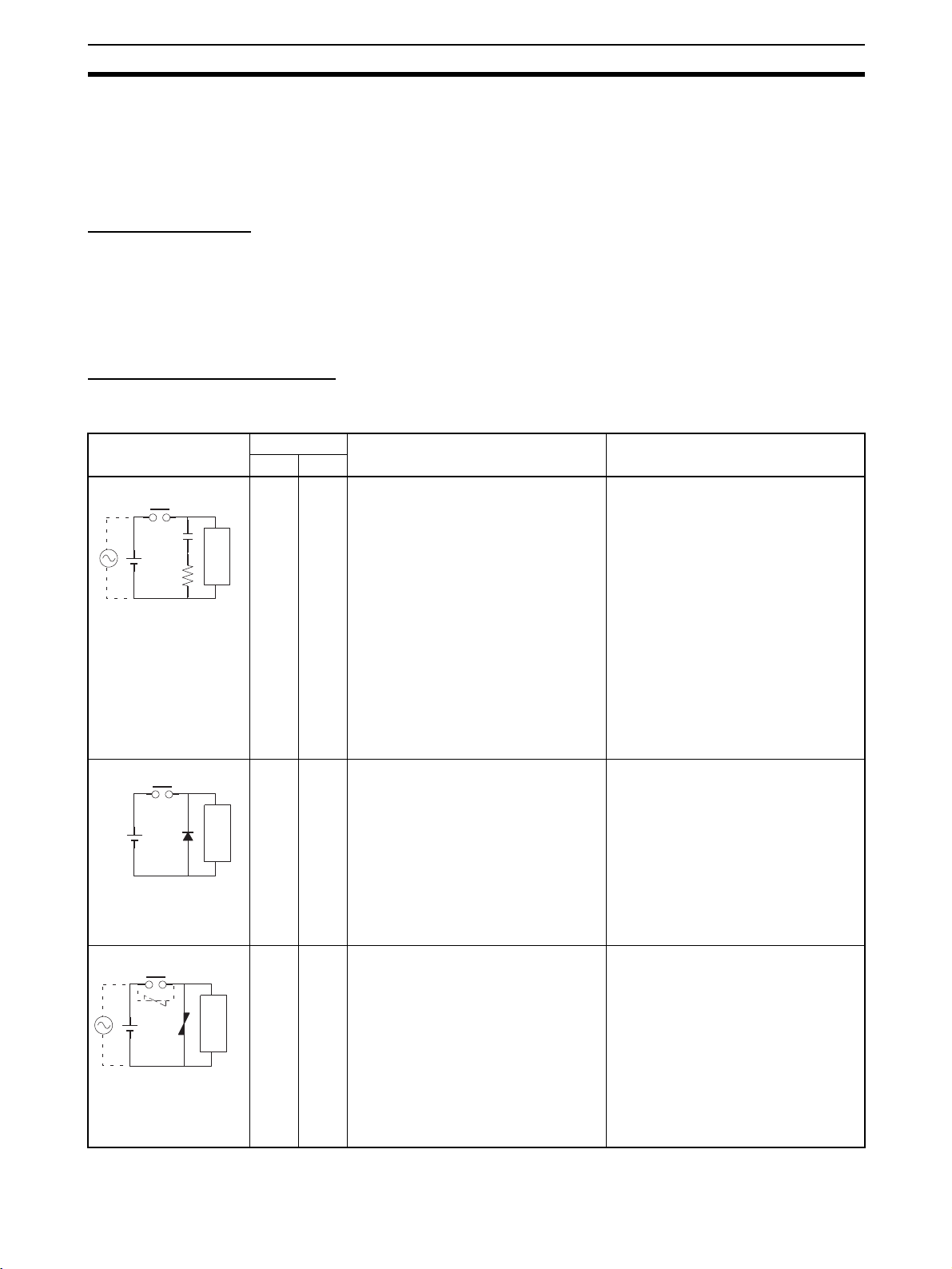
When switching an inductive load, connect a surge protector, diodes, etc., in
parallel with the load or contact as shown below.
Circuit Current Characteristic Required element
AC DC
CR method
Power
supply
Diode method
Power
supply
Varistor method
Power
supply
Yes Yes If the load is a relay or solenoid, there
Inductive
load
No Yes The diode connected in parallel with
Inductive
load
Yes Yes The varistor method prevents the impo-
Inductive
load
is a time lag between the moment the
circuit is opened and the moment the
load is reset.
If the supply voltage is 24 or 48 V,
insert the surge protector in parallel
with the load. If the supply voltage is
100 to 200 V, insert the surge protector
between the contacts.
the load changes energy accumulated
by the coil into a current, which then
flows into the coil so that the current
will be converted into Joule heat by the
resistance of the inductive load.
This time lag, between the moment the
circuit is opened and the moment the
load is reset, caused by this method is
longer than that caused by the CR
method.
sition of high voltage between the contacts by using the constant voltage
characteristic of the varistor. There is
time lag between the moment the circuit is opened and the moment the load
is reset.
If the supply voltage is 24 or 48 V,
insert the varistor in parallel with the
load. If the supply voltage is 100 to 200
V, insert the varistor between the contacts.
The capacitance of the capacitor must
be 1 to 0.5 µF per contact current of
1 A and resistance of the resistor must
be 0.5 to 1 Ω per contact voltage of 1 V.
These values, however, vary with the
load and the characteristics of the
relay. Decide these values from testing,
and take into consideration that the
capacitance suppresses spark discharge when the contacts are separated and the resistance limits the
current that flows into the load when
the circuit is closed again.
The dielectric strength of the capacitor
must be 200 to 300 V. If the circuit is an
AC circuit, use a capacitor with no
polarity.
The reversed dielectric strength value
of the diode must be at least 10 times
as large as the circuit voltage value.
The forward current of the diode must
be the same as or larger than the load
current.
The reversed dielectric strength value
of the diode may be two to three times
larger than the supply voltage if the
surge protector is applied to electronic
circuits with low circuit voltages.
---
xxv
Page 25

Conformance to EC Directives 6
When switching a load with a high inrush current such as an incandescent
lamp, suppress the inrush current as shown below.
Countermeasure 1
OUT
R
COM
Providing a dark current of approx.
one-third of the rated value through
an incandescent lamp
Countermeasure 2
R
OUT
COM
Providing a limiting resistor
xxvi
Page 26

SECTION 1
PC Setup and Other Features
This section explains the PC Setup and other CQM1H features, including interrupt processing and communications. The
PC Setup can be used to control the operating parameters of the CQM1H. To change the PC Setup, refer to the CQM1H
Operation Manual for Programming Console procedures. Refer to the CX-Programmer Operation Manual for CXProgrammer procedures.
If you are not familiar with OMRON PCs or ladder programming, you can read 1-1 PC Setup as an overview of the
operating parameters available for the CQM1H, but may then want to read SECTION 3 Memory Areas, SECTION 4 Ladder-
diagram Programming, and related instructions in SECTION 5 Instruction Set before completing this section.
1-1 PC Setup . . . . . . . . . . . . . . . . . . . . . . . . . . . . . . . . . . . . . . . . . . . . . . . . . . . . . 2
1-1-1 Changing the PC Setup. . . . . . . . . . . . . . . . . . . . . . . . . . . . . . . . . . . 2
1-1-2 Serial Communications Board Settings . . . . . . . . . . . . . . . . . . . . . . 3
1-1-3 PC Setup Settings . . . . . . . . . . . . . . . . . . . . . . . . . . . . . . . . . . . . . . . 4
1-2 Inner Board Settings . . . . . . . . . . . . . . . . . . . . . . . . . . . . . . . . . . . . . . . . . . . . 9
1-2-1 Settings for a Serial Communications Board . . . . . . . . . . . . . . . . . . 9
1-2-2 Settings for a High-speed Counter Board. . . . . . . . . . . . . . . . . . . . . 10
1-2-3 Settings for a Pulse I/O Board . . . . . . . . . . . . . . . . . . . . . . . . . . . . . 11
1-2-4 Settings for an Absolute Encoder Interface Board . . . . . . . . . . . . . . 11
1-2-5 Settings for an Analog I/O Board. . . . . . . . . . . . . . . . . . . . . . . . . . . 12
1-3 Basic PC Operation and I/O Processes . . . . . . . . . . . . . . . . . . . . . . . . . . . . . . 12
1-3-1 Startup Mode . . . . . . . . . . . . . . . . . . . . . . . . . . . . . . . . . . . . . . . . . . 12
1-3-2 Hold Bit Status . . . . . . . . . . . . . . . . . . . . . . . . . . . . . . . . . . . . . . . . . 13
1-3-3 RS-232C Port Servicing Time . . . . . . . . . . . . . . . . . . . . . . . . . . . . . 13
1-3-4 Peripheral Port Servicing Time. . . . . . . . . . . . . . . . . . . . . . . . . . . . . 14
1-3-5 Minimum Cycle Time. . . . . . . . . . . . . . . . . . . . . . . . . . . . . . . . . . . . 14
1-3-6 Input Time Constants . . . . . . . . . . . . . . . . . . . . . . . . . . . . . . . . . . . . 14
1-3-7 High-speed Timers . . . . . . . . . . . . . . . . . . . . . . . . . . . . . . . . . . . . . . 15
1-3-8 DSW(87) Input Digits and Output Refresh Method. . . . . . . . . . . . . 16
1-3-9 Peripheral Port Settings . . . . . . . . . . . . . . . . . . . . . . . . . . . . . . . . . . 16
1-3-10 Error Log Settings. . . . . . . . . . . . . . . . . . . . . . . . . . . . . . . . . . . . . . . 17
1-4 Interrupt Functions . . . . . . . . . . . . . . . . . . . . . . . . . . . . . . . . . . . . . . . . . . . . . 18
1-4-1 Types of Interrupts . . . . . . . . . . . . . . . . . . . . . . . . . . . . . . . . . . . . . . 18
1-4-2 Processing the Same Memory Locations with the Main Program and
Interrupt Subroutines . . . . . . . . . . . . . . . . . . . . . . . . . . . . . . . . . . . . 21
1-4-3 Input Interrupts . . . . . . . . . . . . . . . . . . . . . . . . . . . . . . . . . . . . . . . . . 23
1-4-4 Masking All Interrupts . . . . . . . . . . . . . . . . . . . . . . . . . . . . . . . . . . . 30
1-4-5 Interval Timer Interrupts. . . . . . . . . . . . . . . . . . . . . . . . . . . . . . . . . . 31
1-4-6 High-speed Counter 0 Interrupts . . . . . . . . . . . . . . . . . . . . . . . . . . . 34
1-4-7 High-speed Counter 0 Overflows/Underflows . . . . . . . . . . . . . . . . . 42
1-5 Pulse Output Function. . . . . . . . . . . . . . . . . . . . . . . . . . . . . . . . . . . . . . . . . . . 44
1-6 Communications Functions. . . . . . . . . . . . . . . . . . . . . . . . . . . . . . . . . . . . . . . 47
1-6-1 Host Link and No-protocol Communications Settings. . . . . . . . . . . 48
1-6-2 Host Link Communications Settings and Procedures . . . . . . . . . . . 51
1-6-3 No-protocol Communications Settings and Procedures. . . . . . . . . . 53
1-6-4 One-to-one Data Links . . . . . . . . . . . . . . . . . . . . . . . . . . . . . . . . . . . 55
1-6-5 NT Link 1:1 Mode Communications . . . . . . . . . . . . . . . . . . . . . . . . 57
1-6-6 Wiring Ports . . . . . . . . . . . . . . . . . . . . . . . . . . . . . . . . . . . . . . . . . . . 58
1-7 Calculating with Signed Binary Data . . . . . . . . . . . . . . . . . . . . . . . . . . . . . . . 58
1-7-1 Definition of Signed Binary Data . . . . . . . . . . . . . . . . . . . . . . . . . . . 58
1-7-2 Arithmetic Flags . . . . . . . . . . . . . . . . . . . . . . . . . . . . . . . . . . . . . . . . 59
1-7-3 Inputting Signed Binary Data Using Decimal Values . . . . . . . . . . . 59
1-7-4 Using Signed-binary Expansion Instructions . . . . . . . . . . . . . . . . . . 60
1-7-5 Application Example Using Signed Binary Data. . . . . . . . . . . . . . . 60
1
Page 27

PC Setup Section 1-1
1-1 PC Setup
The PC Setup contains operating parameters that control CQM1H operation.
To make the maximum use of CQM1H functionality when using interrupt processing and communications functions, the PC Setup may be customized
according to operating conditions.
The general PC Setup settings are contained in DM 6600 to DM 6655 and the
Serial Communications Board settings are contained in DM 6550 to DM 6559.
Strictly speaking, the Serial Communications Board settings are part of the
read-only DM area, not the PC Setup, but they are included here because
they are so similar to PC Setup settings.
The PC Setup defaults are set for general operating conditions, so that the
CQM1H can be used without having to change the settings. You are, however,
advised to check the default values before attempting operation.
Default Values The default values for the PC Setup are 0000 for all words. The default values
for DM 6600 to DM 6655 can be reset at any time by turning ON SR 25210.
!Caution When data memory (DM) is cleared from a Programming Device, the PC
Setup settings will also be cleared to all zeros.
1-1-1 Changing the PC Setup
Making Changes from a
Programming Device
Write-protecting the PC
Setup
PC Setup settings are read at various times depending on the setting, as
described below.
• DM 6550 to DM 6559: Read regularly when the power is ON.
• DM 6600 to DM 6614: Read only when PC’s power supply is turned ON.
• DM 6615 to DM 6644: Read only when program execution begins.
• DM 6645 to DM 6655: Read regularly when the power is ON.
Changes in the PC Setup become effective only at the times given above. The
CQM1H will thus have to be restarted to make changes in DM 6600 to
DM 6614 effective, and program execution will have to be restarted to make
changes in DM 6615 to DM 6644 effective.
The PC Setup can be read, but not written, from the user program. Writing
can be done only by using a Programming Console or other Programming
Device.
DM 6600 to DM 6644 can be set or changed only while in PROGRAM mode.
DM 6550 to DM 6559 and DM 6645 to DM 6655 can be set or changed while
in either PROGRAM mode or MONITOR mode.
After PC Setup settings have been made, pin 1 on the DIP switch on the front
of the CPU Unit can be turned ON to prevent Programming Devices from
overwriting the PC Setup. When pin 1 is ON, the user program, the read-only
DM area (DM 6144 to DM 6568), and the PC Setup (DM 6600 to DM 6655)
cannot be overwritten from a Programming Device.
2
Page 28

PC Setup Section 1-1
Errors in the PC Setup If an incorrect PC Setup setting is accessed, a non-fatal error (error code 9B)
will be generated, the corresponding error flag will be turned ON, and the
default setting will be used.
Flag(s) Function
AR 2400 Turns ON when there is an error in DM 6600 to DM 6614 (read when the power is turned ON).
AR 2401 Turns ON when there is an error in DM 6615 to DM 6644 (read at the beginning of operation).
AR 2402 Turns ON when there is an error in DM 6645 to DM 6655 (read regularly when power is ON).
AR 0400 to AR 0407 An error code of 10 is written to this byte when there is an error in DM 6550 to DM 6559 (read reg-
ularly when power is ON).
1-1-2 Serial Communications Board Settings
The following table shows the Serial Communications Board settings in the
DM area. For details, refer to the Serial Communications Board Operation
Manual.
Word(s) Bit(s) Function
Serial Communications Board Settings
The following settings are effective after transfer to the PC. (The settings for port 2 are contained in words DM 6550 to
DM 6554 and the settings for port 1 are contained in words DM 6555 to DM 6559.)
DM 6550
(port 2)
DM 6555
(port 1)
DM 6551
(port 2)
DM 6556
(port 1)
DM 6552
(port 2)
DM 6557
(port 1)
00 to 03 Port Settings
0: Standard (1 start bit, 7-bit data, even parity, 2 stop bits, 9,600 bps)
1: Settings in DM 6551 (DM 6556 for port 1)
04 to 07 CTS Control Settings
0: Disable; 1: Set
08 to 11 Link Words for 1:1 Data Link (when bits 12 to 15 are set to 3)
0: LR 00 to LR 63; 1: LR 00 to LR 31; 2: LR 00 to LR 15
Maximum Programmable Terminal unit number (when bits 12 to 15 are set to 5)
1 to 7
12 to 15 Communications Mode
0: Host Link; 1: No-protocol; 2: 1:1 Data Link Slave; 3: 1:1 Data Link Master; 4: NT Link in 1:1
Mode; 5: NT Link in 1:N Mode; 6: Protocol Macro
00 to 07 Baud Rate
00: 1.2K, 01: 2.4K, 02: 4.8K, 03: 9.6K, 04: 19.2K
08 to 15 Frame Format
Start Length Stop Parity
00: 1bit 7 bits 1 bit Even
01: 1bit 7 bits 1 bit Odd
02: 1bit 7 bits 1 bit None
03: 1bit 7 bits 2 bit Even
04: 1bit 7 bits 2 bit Odd
05: 1bit 7 bits 2 bit None
06: 1 bit 8 bits 1 bit Even
07: 1 bit 8 bits 1 bit Odd
08: 1 bit 8 bits 1 bit None
09: 1 bit 8 bits 2 bit Even
10: 1 bit 8 bits 2 bit Odd
11: 1 bit 8 bits 2 bit None
00 to 15 Transmission Delay (Host Link or No-protocol)
0000 to 9999 (BCD): Set in units of 10 ms, e.g., a setting of 0001 equals 10 ms
3
Page 29

PC Setup Section 1-1
Word(s) Bit(s) Function
DM 6553
(port 2)
DM 6558
(port 1)
DM 6554
(port 2)
DM 6559
(port 1)
00 to 07 Node Number (Host Link)
00 to 31 (BCD)
08 to 11 Start Code Enable (No-protocol)
0: Disable; 1: Set
12 to 15 End Code Enable (No-protocol)
0: Disable (number of bytes received)
1: Set (specified end code)
2: CR, LF
00 to 07 Start Code (No-protocol)
00 to FF (hexadecimal)
08 to 15 When bits 12 to 15 of DM 6553 or DM 6558 are set to 0:
Number of Bytes Received
00: Default setting (256 bytes)
01 to FF: 1 to 255 bytes
When bits 12 to 15 of DM 6553 or DM 6558 are set to 1:
End Code (No-protocol)
00 to FF (hexadecimal)
1-1-3 PC Setup Settings
The following table shows the PC Setup settings in order in the DM area. For
details, refer to the page numbers shown.
Word(s) Bit(s) Function Page
Startup Processing (DM 6600 to DM 6614)
The following settings are effective after transfer to the PC only after the PC is restarted.
DM 6600 00 to 07 Startup Mode (effective when bits 08 to 15 are set to 02).
00: PROGRAM; 01: MONITOR 02: RUN
08 to 15 Startup Mode Designation
00: Depends on CPU Unit DIP switch pin 7 and Programming Console switch settings
01: Continue operating mode last used before power was turned OFF
02: Setting in DM 6600 bits 00 to 07
DM 6601 00 to 07 Not used.
08 to 11 I/O Hold Bit Status (SR 25212)
0: Reset; 1: Maintain
12 to 15 Forced Status Hold Bit Status (SR 25211)
DM 6602 to
DM 6603
DM 6604 to
DM 6610
DM 6611 to
DM 6612
DM 6613 00 to 15 Servicing Time Setting for Serial Communications Board Port 2 9
DM 6614 00 to 15 Servicing Time Setting For Serial Communications Board Port 1
Pulse Output and Cycle Time Settings (DM 6615 to DM 6619)
The following settings are effective after transfer to the PC the next time operation is started.
DM 6615 00 to 07 Word for Pulse Output
00 to 15 Inner Board Slot 1 Settings (See 1-2 Inner Board Settings for details.) 9
00 to 15 Not used.
00 to 15 Inner Board Slot 2 Settings (See 1-2 Inner Board Settings for details.) 9
08 to 15 Not used. Set to 00.
0: Reset; 1: Maintain
00: IR 100; 01: IR101; 02: IR 102... 15: IR 115
Sets the word used for pulse output from an output on a Transistor Output Unit. Pulses
can be output only from one output at a time.
12
13
46
4
Page 30

PC Setup Section 1-1
Word(s) Bit(s) Function Page
DM 6616 00 to 07 Servicing Time for RS-232C Port (when bits 08 to 15 are set to 01)
00 to 99 (BCD): Percentage of cycle time used to service RS-232C port. The servicing
time must be between 0.256 ms and 65.536 ms.
08 to 15 RS-232C Port Servicing Setting Enable
00: 5% of the cycle time
01: Use time in 00 to 07.
(When the PC is stopped, the servicing time will always be 10 ms.)
DM 6617 00 to 07 Servicing Time for Peripheral Port (when bits 08 to 15 are set to 01)
00 to 99 (BCD): Percentage of cycle time used to service peripheral port. The servicing
time must be between 0.256 ms and 65.536 ms.
08 to 15 Peripheral Port Servicing Setting Enable
00: 5% of the cycle time
01: Use time setting in bits 00 to 07.
(When the PC is stopped, the servicing time will always be 10 ms.)
DM 6618 00 to 07 Cycle Monitor Time (when bits 08 to 15 are set to 01, 02, or 03)
00 to 99 (BCD) × setting units (See bits 08 to 15.)
08 to 15 Cycle Monitor Enable
00: 120 ms (setting in bits 00 to 07 disabled)
01: Setting units: 10 ms
02: Setting units: 100 ms
03: Setting units: 1 s
DM 6619 00 to 15 Cycle Time
0000: Variable (no minimum)
0001 to 9999 (BCD): Minimum cycle time in ms
Interrupt Processing (DM 6620 to DM 6639)
The following settings are effective after transfer to the PC the next time operation is started.
DM 6620 00 to 03 Input Time Constant for IR 00000 to IR 00007
0: 8 ms; 1: 1 ms; 2: 2 ms; 3: 4 ms; 4: 8 ms; 5: 16 ms; 6: 32 ms; 7: 64 ms; 8: 128 ms
04 to 07 Input Time Constant for IR 00008 to IR 00015 (Setting same as bits 00 to 03)
08 to 11 Input Time Constant for IR 001 (Setting same as bits 00 to 03)
12 to 15 Not used. Set to 0.
DM 6621 00 to 07 Input Constant for IR 002
00: 8 ms; 01: 1 ms; 02: 2 ms; 03: 4 ms; 04: 8 ms; 05: 16 ms; 06: 32 ms; 07: 64 ms;
08: 128 ms
08 to 15 Input Constant for IR 003 (Setting same as for IR 002.)
DM 6622 00 to 07 Input Constant for IR 004 (Setting same as for IR 002.)
08 to 15 Input Constant for IR 005 (Setting same as for IR 002.)
DM 6623 00 to 07 Input Constant for IR 006 (Setting same as for IR 002.)
08 to 15 Input Constant for IR 007 (Setting same as for IR 002.)
DM 6624 00 to 07 Input Constant for IR 008 (Setting same as for IR 002.)
08 to 15 Input Constant for IR 009 (Setting same as for IR 002.)
DM 6625 00 to 07 Input Constant for IR 010 (Setting same as for IR 002.)
08 to 15 Input Constant for IR 011 (Setting same as for IR 002.)
DM 6626 00 to 07 Input Constant for IR 012 (Setting same as for IR 002.)
08 to 15 Input Constant for IR 013 (Setting same as for IR 002.)
DM 6627 00 to 07 Input Constant for IR 014 (Setting same as for IR 002.)
08 to 15 Input Constant for IR 015 (Setting same as for IR 002.)
DM 6628 00 to 03 Interrupt Enable for IR 00000
0: Normal input; 1: Interrupt input in Interrupt Input Mode or Counter Mode
04 to 07 Interrupt Enable for IR 00001
0: Normal input; 1: Interrupt input in Interrupt Input Mode or Counter Mode
08 to 11 Interrupt Enable for IR 00002
0: Normal input; 1: Interrupt input in Interrupt Input Mode or Counter Mode
12 to 15 Interrupt Enable for IR 00003
0: Normal input; 1: Interrupt input in Interrupt Input Mode or Counter Mode
13
14
17
14
14
14
26
5
Page 31

PC Setup Section 1-1
Word(s) Bit(s) Function Page
DM 6629 00 to 07 Number of TIMH(15) High-speed Timers to Refresh by Interrupt Refreshing
08 to 15 High-speed Timer Interrupt Refresh Enable
DM 6630 00 to 07 First Input Refresh Word for I/O Interrupt 0: 00 to 11 (BCD) 26
08 to 15 Number of Input Refresh Words for I/O Interrupt 0: 00 to 12 (BCD)
DM 6631 00 to 07 First Input Refresh Word for I/O Interrupt 1: 00 to 11 (BCD)
08 to 15 Number of Input Refresh Words for I/O interrupt 1: 00 to 12 (BCD)
DM 6632 00 to 07 First Input Refresh Word for I/O Interrupt 2: 00 to 11 (BCD)
08 to 15 Number of Input Refresh Words for I/O Interrupt 2: 00 to 12 (BCD)
DM 6633 00 to 07 First Input Refresh Word for I/O Interrupt 3: 00 to 11 (BCD)
08 to 15 Number of Input Refresh Words for I/O Interrupt 3: 00 to 12 (BCD)
DM 6634 00 to 07 First Input Refresh Word for High-speed Counter 1: 00 to 11 (BCD) 26
08 to 15 Number of Input Refresh Words for High-speed Counter 1: 00 to 12 (BCD)
DM 6635 00 to 07 First Input Refresh Word for High-speed Counter 2: 00 to 11 (BCD) 26
08 to 15 Number of Input Refresh Words for High-speed Counter 2: 00 to 12 (BCD)
DM 6636 00 to 07 First Input Refresh Word for Interval Timer 0: 00 to 15 (BCD) 32, 39
08 to 15 Number of Input Refresh Words for Interval Timer 0: 00 to 16 (BCD)
DM 6637 00 to 07 First Input Refresh Word for Interval Timer 1: 00 to 15 (BCD)
08 to 15 Number of Input Refresh Words for Interval Timer 1: 00 to 16 (BCD)
DM 6638 00 to 07 First Input Refresh Word for Interval Timer 2 or High-speed Counter 0:
08 to 15 Number of Input Refresh Words for Interval Timer 2 or High-speed Counter 0:
DM 6639 00 to 07 Output Refresh Method
08 to 15 Number of Digits for DIGITAL SWITCH (DSW(87)) Instruction
High-speed Counter Settings (DM 6640 to DM 6644)
The following settings are effective after transfer to the PC the next time operation is started.
DM 6640 to
DM 6641
DM 6642 00 to 03 High-speed Counter 0 Input Mode
DM 6643 to
DM 6644
00 to 15 Inner Board Slot 1 Settings (See 1-2 Inner Board Settings for details.) 9
04 to 07 High-speed Counter 0 Reset Mode
08 to 15 High-speed Counter 0 Enable
00 to 15 Inner Board Slot 2 Settings (See 1-2 Inner Board Settings for details.) 9
00 to 15 (BCD; e.g., set 3 for timers 00 to 02)
00: 16 timers (setting in bits 00 to 07 disabled)
01: Use setting in 00 to 07
00 to 15 (BCD)
00 to 16 (BCD)
00: Cyclic; 01: Direct
00: 4 digits; 01: 8 digits
0: Differential phase mode; 4: Incrementing mode
0: Phase-Z and software reset; 1: Software reset only
00: Don’t use high-speed counter 0; 01: Use high-speed counter 0.
15
16, 475
16, 427
39
6
Page 32

PC Setup Section 1-1
Word(s) Bit(s) Function Page
RS-232C Port Settings
The following settings are effective after transfer to the PC.
DM 6645 00 to 03 Port Settings (Host Link or No-protocol mode)
0: Standard (1 start bit, 7-bit data, even parity, 2 stop bits, 9,600 bps)
1: Settings in DM 6646
04 to 07 CTS Control Settings (Host Link or No-protocol mode)
0: Disable; 1: Set
08 to 11 Link Words for 1:1 Data Link (1:1 data link master mode)
0: LR 00 to LR 63; 1: LR 00 to LR 31; 2: LR 00 to LR 15
12 to 15 Communications Mode
0: Host Link; 1: No-protocol; 2: 1:1 Data Link Slave; 3: 1:1 Data Link Master; 4: NT Link
in 1:1 Mode
DM 6646 00 to 07 Baud Rate
00: 1.2 kbps, 01: 2.4 kbps, 02: 4.8 kbps, 03: 9.6 kbps, 04: 19.2 kbps
08 to 15 Frame Format
Start Length Stop Parity
00: 1 bit 7 bits 1 bit Even
01: 1 bit 7 bits 1 bit Odd
02: 1 bit 7 bits 1 bit None
03: 1 bit 7 bits 2 bit Even
04: 1 bit 7 bits 2 bit Odd
05: 1 bit 7 bits 2 bit None
06: 1 bit 8 bits 1 bit Even
07: 1 bit 8 bits 1 bit Odd
08: 1 bit 8 bits 1 bit None
09: 1 bit 8 bits 2 bit Even
10: 1 bit 8 bits 2 bit Odd
11: 1 bit 8 bits 2 bit None
DM 6647 00 to 15 Transmission Delay (Host Link or No-protocol)
0000 to 9999 (BCD): Set in units of 10 ms, e.g., a setting of 0001 equals 10 ms
DM 6648 00 to 07 Node Number (Host Link): 00 to 31 (BCD) 47
08 to 11 Start Code Enable (No-protocol)
0: Disable; 1: Set
12 to 15 End Code Enable (No-protocol)
0: Disable (number of bytes received)
1: Set (specified end code)
2: CR, LF
DM 6649 00 to 07 Start Code (No-protocol)
00 to FF (hexadecimal)
08 to 15 When bits 12 to 15 of DM 6648 are set to 0:
Number of Bytes Received
00: Default setting (256 bytes)
01 to FF: 1 to 255 bytes
When bits 12 to 15 of DM 6648 are set to 1:
End Code (No-protocol)
00 to FF (hexadecimal)
47
7
Page 33

PC Setup Section 1-1
Word(s) Bit(s) Function Page
Peripheral Port Settings
The following settings are effective after transfer to the PC.
DM 6650 00 to 03 Port Settings (Host Link or No-protocol mode)
0: Standard (1 start bit, 7-bit data, even parity, 2 stop bits, 9,600 bps)
1: Settings in DM 6651
04 to 07 CTS Control Settings (Host Link or No-protocol mode)
0: Disable; 1: Set
08 to 11 Not used.
12 to 15 Communications Mode (when bits 00 to 03 are set to 1)
0: Host Link; 1: No-protocol
When a Programming Console is connected to the peripheral port, turn OFF pin 7 of
the CPU Unit’s DIP switch. (Pin 5 and the PC Setup settings are disabled in this case.)
When connecting a personal computer to the peripheral port for use as a Programming
Device, turn pin 7 ON and set the communications mode to “Host Link.” When these
settings have been made and the personal computer is set for peripheral bus opera-
tion, the CPU Unit’s peripheral port communications mode will automatically switch to
peripheral bus mode.
DM 6651 00 to 07 Baud Rate (Host Link, peripheral bus, or No-protocol mode)
00: 1.2 kbps, 01: 2.4 kbps, 02: 4.8 kbps, 03: 9.6 kbps, 04: 19.2 kbps
08 to 15 Frame Format (Host Link or No-protocol mode)
Start Length Stop Parity
00: 1 bit 7 bits 1 bit Even
01: 1 bit 7 bits 1 bit Odd
02: 1 bit 7 bits 1 bit None
03: 1 bit 7 bits 2 bit Even
04: 1 bit 7 bits 2 bit Odd
05: 1 bit 7 bits 2 bit None
06: 1 bit 8 bits 1 bit Even
07: 1 bit 8 bits 1 bit Odd
08: 1 bit 8 bits 1 bit None
09: 1 bit 8 bits 2 bit Even
10: 1 bit 8 bits 2 bit Odd
11: 1 bit 8 bits 2 bit None
DM 6652 00 to 15 Transmission Delay (No-protocol or Slave-initiated Host Link communications only)
0000 to 9999 (BCD): Set in units of 10 ms, e.g., a setting of 0001 equals 10 ms
DM 6653 00 to 07 Node Number (Host Link): 00 to 31 (BCD)
08 to 11 Start Code Enable (No-protocol)
0: Disable; 1: Set
12 to 15 End Code Enable (No-protocol)
0: Disable (number of bytes received)
1: Set (specified end code)
2: CR, LF
DM 6654 00 to 07 Start Code (No-protocol)
00 to FF (hexadecimal)
08 to 15 When bits 12 to 15 of DM 6653 are set to 0:
Number of Bytes Received
00: Default setting (256 bytes)
01 to FF: 1 to 255 bytes
When bits 12 to 15 of DM 6653 are set to 1:
End Code (No-protocol)
00 to FF (hexadecimal)
16, 47
47
47
8
Page 34

Inner Board Settings Section 1-2
Word(s) Bit(s) Function Page
Error Log Settings (DM 6655)
The following settings are effective after transfer to the PC.
DM 6655 00 to 03 Style
0: Shift after 10 records have been stored
1: Store only first 10 records (no shifting)
2 to F: Do not store records
04 to 07 Not used. Set to 0.
08 to 11 Cycle Time Monitor Enable
0: Detect long cycles as non-fatal errors
1: Do not detect long cycles
12 to 15 Low Battery Error Enable
0: Detect low battery voltage as non-fatal error
1: Do not detect low battery voltage
17
1-2 Inner Board Settings
This section explains the PC Setup settings related to Inner Boards mounted
in Inner Board slots 1 and 2.
1-2-1 Settings for a Serial Communications Board
Use the settings in DM 6613 and DM 6614 to set the servicing times for a
Serial Communications Board mounted in Inner Board slot 1. (A Serial Communications Board cannot be mounted in slot 2.)
Word Bits Function
DM 6613 00 to 07 Servicing Time for Serial Communications Board Port 2
08 to 15 Serial Communications Board Port 2 Servicing Setting
DM 6614 00 to 07 Servicing Time for Serial Communications Board Port 1
08 to 15 Serial Communications Board Port 1 Servicing Setting
(enabled by bits 08 to 15)
00 to 99 (BCD): Sets the percentage of the cycle time used to
service port 2. The servicing time must be between 0.256 ms
and 65.536 ms.
00: Fixed at 5% of the cycle time.
01: Use time setting in bits 00 to 07.
(When the PC is stopped, the servicing time will always be
10 ms.)
(enabled by bits 08 to 15)
00 to 99 (BCD): Sets the percentage of the cycle time used to
service port 1. The servicing time must be between 0.256 ms
and 65.536 ms.
00: Fixed at 5% of the cycle time.
01: Use time setting in bits 00 to 07.
(When the PC is stopped, the servicing time will always be
10 ms.)
9
Page 35

Inner Board Settings Section 1-2
1-2-2 Settings for a High-speed Counter Board
The settings in DM 6602, DM 6640, and DM 6641 determine the operation of
a High-speed Counter Board mounted in Inner Board slot 1.
The settings in DM 6611, DM 6643, and DM 6644 determine the operation of
a High-speed Counter Board mounted in Inner Board slot 2.
Word Bits Function Settings
DM 6602
(Slot 1)
DM 6611
(Slot 2)
DM 6640
(Slot 1)
DM 6643
(Slot 2)
DM 6641
(Slot 1)
DM 6644
(Slot 2)
00 High-speed Counter PV Data Format OFF: 8-digit hexadeci-
mal
ON: 8-digit BCD
01 to 07 Not used Set to 0.
08 External Output Transistor Selector OFF: Sourcing
09 to 15 Not used. Set to 0.
00 to 03 High-speed Counter 1 Input Mode See note 1.
04 to 07 High-speed Counter 1 Count Fre-
quency, Numeric Range, and
Counter Reset Mode
08 to 11 High-speed Counter 2 Input Mode See note 1.
12 to 15 High-speed Counter 2 Count Fre-
quency, Numeric Range, and
Counter Reset Mode
00 to 03 High-speed Counter 3 Input Mode See note 1.
04 to 07 High-speed Counter 3 Count Fre-
quency, Numeric Range, and
Counter Reset Mode
08 to 11 High-speed Counter 4 Input Mode See note 1.
12 to 15 High-speed Counter 4 Count Fre-
quency, Numeric Range, and
Counter Reset Mode
ON: Sinking
See note 2.
See note 2.
See note 2.
See note 2.
Note 1. The settings for the high-speed counter input mode are as follows:
Setting Input Mode
0 Hex Differential Phase Inputs, 1x
1 Hex Differential Phase Inputs, 2x
2 Hex Differential Phase Inputs, 4x
3 Hex Up/Down Input
4 Hex Pulse/Direction Input
2. The settings for the high-speed counter count frequency, numeric range,
and counter reset mode are as follows:
Setting Count frequency Numeric range Reset mode
0 Hex 50 kHz Linear Counting Phase-Z + Software Reset
1 Hex Software Reset Only
2 Hex Ring Counting Phase-Z + Software Reset
3 Hex Software Reset Only
4 Hex 500 kHz Linear Counting Phase-Z + Software Reset
5 Hex Software Reset Only
6 Hex Ring Counting Phase-Z + Software Reset
7 Hex Software Reset Only
10
Page 36

Inner Board Settings Section 1-2
1-2-3 Settings for a Pulse I/O Board
The settings in DM 6611, DM 6643, and DM 6644 determine the operation of
a Pulse I/O Board mounted in Inner Board slot 2. (A Pulse I/O Board cannot
be mounted in slot 1.)
Word Bits Function
DM 6611 00 to 15 Mode Setting for Ports 1 and 2
0000: High-speed Counter Mode
0001: Simple Positioning Mode
DM 6643 00 to 03 Port 1 Input Mode
04 to 07 Port 1 Counter Reset Method
08 to 11 Port 1 Numeric Range
12 to 15 Port 1 Pulse Output Duty Factor
DM 6644 00 to 03 Port 2 Input Mode
04 to 07 Port 2 Counter Reset Method
08 to 11 Port 2 Numeric Range
12 to 15 Port 2 Pulse Output Duty Factor
0: Differential Phase Mode
1: Pulse/Direction Mode
2: Up/Down Mode
0: Phase-Z and software reset; 1: Software reset only
0: Linear counting; 1: Ring counting
0: Fixed duty factor; 1: Variable duty factor
0: Differential Phase Mode
1: Pulse/Direction Mode
2: Up/Down Mode
0: Phase-Z and software reset; 1: Software reset only
0: Linear counting; 1: Ring counting
0: Fixed duty factor; 1: Variable duty factor
1-2-4 Settings for an Absolute Encoder Interface Board
The settings in DM 6611, DM 6612, DM 6643, and DM 6644 determine the
operation of an Absolute Encoder Interface Board mounted in Inner Board slot
2. (An Absolute Encoder Interface Board cannot be mounted in slot 1.)
Word Bits Function
DM 6611 00 to 15 Origin Compensation for Port 1 (4-digit BCD)
Origin will be compensated when the Port 1 Origin Compensation Bit (SR 25201) is turned ON. The compensation value will
be recorded in BCD between 0000 and 4095 whether the
counter is set to BCD mode or 360° mode.
DM 6612 00 to 15 Origin Compensation for Port 2 (4-digit BCD)
Origin will be compensated when the Port 2 Origin Compensation Bit (SR 25202) is turned ON. The compensation value will
be recorded in BCD between 0000 and 4095 whether the
counter is set to BCD mode or 360° mode.
DM 6643 00 to 07 Port 1 Input Resolution
08 to 15 Port 1 Operating Mode
DM 6644 00 to 07 Port 2 Input Resolution
08 to 15 Port 2 Operating Mode
00: 8 bits; 01: 10 bits; 02: 12 bits
00: BCD mode; 01: 360° mode
00: 8 bits; 01: 10 bits; 02: 12 bits
00: BCD mode; 01: 360° mode
11
Page 37

Basic PC Operation and I/O Processes Section 1-3
1-2-5 Settings for an Analog I/O Board
The settings in DM 6611 determine the operation of an Analog I/O Board
mounted in Inner Board slot 2. (An Analog I/O Board cannot be mounted in
slot 1.)
Word Bits Function Settings
DM 6611 00 to 01 Analog Input 1 Input Signal Range Set the bit status of the
02 to 03 Analog input 2 Input Signal Range
04 to 05 Analog input 3 Input Signal Range
06 to 07 Analog input 4 Input Signal Range
08 Analog Input 1 Usage Selection 0: Support (use) input.
09 Analog Input 2 Usage Selection
10 Analog Input 3 Usage Selection
11 Analog Input 4 Usage Selection
12 to 15 Not used. Set to 0.
two bits as follows:
00: –10 to +10 V
01: 0 to 10 V
10: 0 to 5 V or
0 to 20 mA
1: Do not support input.
1-3 Basic PC Operation and I/O Processes
This section explains the PC Setup settings related to basic operation and I/O
processes.
1-3-1 Startup Mode
The operating mode the PC will start in when power is turned ON can be set
as shown below.
15
Bit
DM 6600
Startup Mode Designation
00: Depends upon Programming Device and DIP switch settings (See table below.)
01: Operating mode last used before power was turned OFF
02: Mode set in bits 00 to 07
Startup Mode (Bits 08 to 15: Valid when bits 00 to 07 are set to 02)
00: PROGRAM mode
01: MONITOR mode
02: RUN mode
Default: Operating mode determined by Programming Device and DIP switch settings
Programming Device
connected at startup
None connected. OFF PROGRAM mode
Programming Console
connected.
Other Programming
Device connected.
as shown in the table below.
Pin 7 of the CPU
Unit’s DIP switch
ON RUN mode
OFF Operating mode set on the Program-
ON PROGRAM mode (See note 1.)
OFF PROGRAM mode (See note 1.)
ON Depends upon the Connecting Cable
Startup mode
ming Console’s mode switch
being used. (See note 2.)
0
12
Note 1. In these cases, the CQM1H will not be able to communicate with the con-
nected Programming Device.
Page 38

Basic PC Operation and I/O Processes Section 1-3
2. The startup mode will be PROGRAM mode or RUN mode, depending on
the Connecting Cable being used.
Connecting Cable Startup mode
CS1W-CN114 + CQM1-CIF01/02 PROGRAM mode
CS1W-CN118 + XW2Z-200/500S(-V) PROGRAM mode
CS1W-CN226/626 RUN mode
CS1W-CN118 + XW2Z-200/500S-CV RUN mode
1-3-2 Hold Bit Status
Make the settings shown below to determine whether, when the power supply
is turned ON, the Forced Status Hold Bit (SR 25211) and/or I/O Hold Bit
(SR 25212) will retain the status that was in effect when the power was last
turned OFF, or whether the previous status will be cleared.
15 0
Bit
DM 6601
0 0
The Forced Status Hold Bit (SR 25211) determines whether or not the forced
set/reset status is retained when changing from PROGRAM mode to MONITOR mode.
The I/O Hold Bit (SR 25212) determines whether or not the status of IR bits
and LR bits is retained when PC operation is started and stopped.
1-3-3 RS-232C Port Servicing Time
The following settings are used to determine the percentage of the cycle time
devoted to servicing the RS-232C port.
Servicing time setting enable
00: Disabled (5% of the cycle time)
01: Enabled (setting in bits 00 to 07 used)
Servicing time (%, valid when bits 08 to 15 are set to 01)
00 to 99 (BCD, two digits)
Default: 5% of cycle time
SR 25211 setting
0: Clear status
1: Retain status
SR 25212 setting
0: Clear status
1: Retain status
Default: Clear both.
Always 00
Bit
DM 6616
15 0
Example: If DM 6616 is set to 0110, the RS-232C port will be serviced for
10% of the cycle time.
The minimum servicing time is 0.256 ms.
The entire servicing time will not be used unless processing requests exist.
13
Page 39

Basic PC Operation and I/O Processes Section 1-3
1-3-4 Peripheral Port Servicing Time
The following settings are used to determine the percentage of the cycle time
devoted to servicing the peripheral port.
15 0
Bit
DM 6617
Servicing time setting enable
00: Disabled (5% of the cycle time)
01: Enabled (setting in bits 00 to 07 used)
Servicing time (%, valid when bits 08 to 15 are set to 01)
00 to 99 (BCD, two digits)
Default: 5% of cycle time
Example: If DM 6617 is set to 0115, the peripheral port will be serviced for
15% of the cycle time.
The minimum servicing time is 0.256 ms.
The entire servicing time will not be used unless processing requests exist.
1-3-5 Minimum Cycle Time
Make the settings shown below to standardize the cycle time and to eliminate
variations in I/O response time by setting a minimum cycle time.
If the actual cycle time is shorter than the minimum cycle time, execution will
wait until the minimum time has expired. If the actual cycle time is longer than
the minimum cycle time, then operation will proceed according to the actual
cycle time. AR 2405 will turn ON if the minimum cycle time is exceeded.
1-3-6 Input Time Constants
Make the settings shown below to set the time from when the actual inputs
from the DC Input Unit are turned ON or OFF until the corresponding input
bits are updated (i.e., until their ON/OFF status is changed). Make these settings when you want to adjust the time until inputs stabilize.
Increasing the input time constant can reduce the effects from chattering and
external noise.
Input from an input device
such as a limit switch
15 0
Bit
DM 6619
Cycle time (4-digit BCD)
0000:Cycle time variable
0001 to 9999: Minimum cycle time (Unit: 1 ms)
Default: Cycle time variable
14
Input bit status
t
t
Input time constant
Page 40

Basic PC Operation and I/O Processes Section 1-3
Input Time Constants for IR 000 and IR 001
15 0
Bit
DM 6620
Time constant for IR 00100 to IR 00115 (1-digit BCD; see below.)
Time constant for IR 00008 to IR 00015 (1 digit BCD; see below.)
Time constant for IR 00000 to IR 00007 (1 digit BCD; see below.)
Default: 0000 (8 ms for each)
Input Time Constants for IR 002 to IR 015
DM 6621: IR 002 and IR 003
DM 6622: IR 004 and IR 005
DM 6623: IR 006 and IR 007
DM 6624: IR 008 and IR 009
DM 6625: IR 010 and IR 011
DM 6626: IR 012 and IR 013
DM 6627: IR 014 and IR 015
Time constant for IR 003, IR 005, IR 007, IR 009, IR 011, IR 013, and IR 015
Time constant for IR 002, IR 004, IR 006, IR 008, IR 010, IR 012, and IR 014
Default: 0000 (8 ms for each)
DM 6621 to DM 6627
0
15 0
Bit
The nine possible settings for the input time constant are shown below. Set
only the rightmost digit for IR 000.
0: 8 ms 1: 1 ms 2: 2 ms 3: 4 ms 4: 8 ms
5: 16 ms 6: 32 ms 7: 64 ms 8: 128 ms
1-3-7 High-speed Timers
Make the settings shown below to set the number of high-speed timers created with TIMH(15) that will use interrupt processing.
High-speed timer interrupt setting enable
00: Setting disabled (Interrupt processing for all high-speed timers, TIM 000 to TIM 015)
01: Enabled (Use setting in bits 00 to 07.)
Number of high-speed timer for interrupts (valid when bits 08 to 15 are 01)
00 to 15 (2-digit BCD)
Default: Interrupt processing for all high-speed timers,TIM 000 to TIM 015.
The setting indicates the number of timers that will use interrupt processing
beginning with TIM 000. For example, if “0108” is specified, then eight timers,
TIM 000 to TIM 007 will use interrupt processing.
Note 1. High-speed timers will not be accurate without interrupt processing unless
the cycle time is 10 ms or less.
2. If the SPED(64) instruction is used and pulses are output at a frequency of
500 Hz or greater, then set the number of high-speed timers with interrupt
processing to four or less. Refer to information on the SPED(64) instruction
for details.
3. Interrupt response time for other interrupts will be improved if interrupt processing is set to 00 when high-speed timer processing is not required. This
includes any time the cycle time is less than 10 ms.
Bit
DM 6629
15 0
15
Page 41

Basic PC Operation and I/O Processes Section 1-3
1-3-8 DSW(87) Input Digits and Output Refresh Method
Make the settings shown below to set the number of input digits for the
DSW(87) instruction, and to set the output refresh method.
15 0
Bit
DM 6639
Number of input digits for the DSW(87)
00: 4 digits
01: 8 digits
Output refresh method
00: Cyclic
01: Direct
Default: The number of input digits for the DSW(87) instruction is set to "4" and the output refresh method is cyclic.
Refer to page 427 for details on the DSW(87) instruction and to SECTION 7
CPU Unit Operation and Processing Time for details on I/O refresh methods.
1-3-9 Peripheral Port Settings
Serial communications settings for the peripheral port are determined by pins
5 and 7 of the CPU Unit’s DIP switch, the hexadecimal setting in DM 6650,
and the device connected to the peripheral port.
DIP switch
settings
Pin 5 Pin 7
OFF OFF Ignored Programming Console Programming Console bus
OFF ON 0000 Programming Device
ON OFF Ignored Programming Console Programming Console bus
ON ON Ignored Programming Device
DM 6650
setting
0001 Host Link, custom settings
10@@ No-protocol
Connected device Serial communications mode
other than a Programming Console (such as
a personal computer)
other than a Programming Console (such as
a personal computer)
Host Link, standard settings
Peripheral bus mode if CX-Programmer is set for peripheral
bus.
Peripheral bus mode if CX-Programmer is set for peripheral
bus.
Host Link, standard settings
Peripheral bus mode if CX-Programmer is set for peripheral
bus.
16
Page 42

Basic PC Operation and I/O Processes Section 1-3
1-3-10 Error Log Settings
Make the settings shown below for detecting errors and storing the error log.
Cycle Monitor Time
(DM 6618)
Note 1. The units used for the maximum and current cycle times recorded in AR
The cycle monitor time is used for checking for extremely long cycle times, as
can happen when the program goes into an infinite loop. If the cycle time
exceeds the cycle monitor setting, a fatal error (FALS 9F) will be generated.
15 0
Bit
DM 6618
Cycle Monitor Time Enable and Unit
00: Setting disabled (time fixed at 120 ms)
01: Setting in 00 to 07 enabled; unit:10 ms
02: Setting in 00 to 07 enabled; unit:100 ms
03: Setting in 00 to 07 enabled; unit:1 s
Cycle monitor time setting (When bits 08 to 15 are not 00)
00 to 99 (2-digit BCD; unit set in bits 08 to 15.)
Default: 120 ms.
26 and AR 27 (4-digit BCD) depend on the unit set for the cycle monitor
time in DM 6618, as shown below.
Bits 08 to 15 set to 01: 0.1 ms
Bits 08 to 15 set to 02: 1 ms
Bits 08 to 15 set to 03: 10 ms
2. If the cycle time is 1 s or longer, the cycle time read from Programming Devices will be 999.9 ms. The correct maximum and current cycle times will
be recorded in the AR area.
Example
If 0230 is set in DM 6618, an FALS 9F error will not occur until the cycle time
exceeds 3 s. If the actual cycle time is 2.59 s, the current cycle time stored in
the AR area will be 2590 (ms), but the cycle time read from a Programming
Device will be 999.9 ms.
A “cycle time over” error (non-fatal) will be generated when the cycle time
exceeds 100 ms unless detection of long cycle times is disable using the setting in DM 6655.
17
Page 43

Interrupt Functions Section 1-4
Error Detection and Error
Log Operation (DM 6655)
Make the settings shown below to determine whether or not a non-fatal error
is to be generated when the cycle time exceeds 100 ms or when the voltage
of the built-in battery drops, and to set the method for storing records in the
error log when errors occur.
Low battery voltage detection
0: Detect
1: Don't detect
Cycle time over detection
0: Detect
1: Don't detect
Error log storage method
0: Error records for 10 most recent errors always stored (older errors deleted).
1: Only first 10 error records stored (no errors stored beyond that point).
2 to F: Error records not stored.
Default: Low battery voltage and cycle time over errors detected, and error records
stored for the 10 most recent errors.
Battery errors and cycle time overrun errors are non-fatal errors. For details
on the error log, refer to SECTION 8 Troubleshooting.
1-4 Interrupt Functions
Bit
DM 6655
15 0
0
Always 0
This section explains the settings and methods for using the CQM1H interrupt
functions.
1-4-1 Types of Interrupts
The CQM1H has four types of interrupts, as outlined below.
Input Interrupts:
Interrupt processing is executed when an input from an external source to one
of CPU Unit bits IR 00000 to IR 00003 turns ON.
Interval Timer Interrupts:
Interrupt processing is executed by an interval timer with a precision of 0.1
ms.
High-speed Counter Interrupts:
Interrupt processing is executed according to the present value (PV) of the
built-in high-speed counter. CQM1H CPU Units are equipped with the following 3 types of high-speed counter interrupts. All can function as target-value
interrupts or range-comparison interrupts. (A target-value interrupt is generated when the PV matches the SV, and a range-comparison interrupt is generated when the PV is within a preset SV range.)
1,2,3... 1. High-speed counter 0 (built into the CPU Unit)
High-speed counter 0 counts pulse inputs to CPU Unit inputs 4 to 6. Twophase pulses up to 2.5 kHz can be counted.
2. High-speed counters 1 and 2 (Pulse I/O Board)
High-speed counters 1 and 2 count high-speed pulse inputs to ports 1 and
2 on the Pulse I/O Board. Two-phase pulses up to 25 kHz can be counted.
3. Absolute high-speed counters 1 and 2 (Absolute Encoder Interface Board)
High-speed counters 1 and 2 count absolute rotary encoder codes input to
ports 1 and 2 on the Absolute Encoder Interface Board.
18
Page 44

Interrupt Functions Section 1-4
Note Interrupt processing is not performed for high-speed counters 1, 2, 3, and 4
on a High-speed Counter Board. A High-speed Counter Board can count
pulses up to 50 kHz or 500 kHz. The high-speed counter PVs can be checked
against a target value or an SV range and a bit pattern can be output internally or externally instead of generating an interrupt.
Serial Communications Board Interrupts:
Interrupt processing is requested from the CPU Unit when the Serial Communications Board receives the desired message.
Interrupt Processing When an interrupt is generated, the specified interrupt subroutine is executed.
Defining Subroutines
Just as with ordinary subroutines, interrupt subroutines are defined using
SBN(92) and RET(93) at the end of the main program.
When interrupt subroutines are executed, a specified range of input bits can
be refreshed.
When an interrupt subroutine is defined, a “no SBS error” will be generated
during the program check but execution will proceed normally. If this error
occurs, check all normal subroutines to be sure that SBS(91) has been programmed before proceeding.
Interrupt Priority
Interrupts have the following order of priority. Input interrupts and interrupts
from high-speed counters 1 and 2 have the highest priority and the interrupt
notification from a Serial Communications Board has the lowest.
1,2,3... 1. Input interrupt 0 > Input interrupt 1 > Input interrupt 2 > Input interrupt 3
Pulse Output Instructions
and Interrupts
Input
interrupts
High-speed counter
1 or 2 interrupts
(from Pulse I/O
=
Board or Absolute
Encoder Interface
Board)
Interval timer
>=
interrupts
High-speed
counter 0
interrupt
Interrupt
notification from
>
Serial
Communications
Board
When an interrupt with a higher priority is received during interrupt processing, the current processes will be stopped and the newly received interrupt will
be processed instead. After that routine has been completely executed, then
processing of the previous interrupt will be resumed.
When an interrupt with a lower or equal priority is received during interrupt
processing, then the newly received interrupt will be processed as soon as the
routine currently being processed has been completely executed.
If two interrupts with the same priority level occur simultaneously, the interrupts will be executed in the following order:
> High-speed counter interrupt 1 > High-speed counter interrupt 2
2. Interval timer interrupt 0 > Interval timer interrupt 1 > Interval timer interrupt
2 (Interval timer interrupt 2 is high-speed counter interrupt 0.)
The following instructions cannot be executed in an interrupt subroutine when
an instruction that controls pulse I/O or high-speed counters is being executed
in the main program: (SR 25503 turns ON)
INI(89), PRV(62), CTBL(63), SPED(64), PULS(65), PWM(––), PLS2(––)
and ACC(––)
19
Page 45

Interrupt Functions Section 1-4
The following methods can be used to circumvent this limitation:
Method 1
All interrupt processing can be masked while the instruction is being executed.
@INT(89)
100
000
000
@PLS2(−−)
001
000
DM 0010
@INT(89)
200
000
000
Method 2
Execute the instruction again in the main program.
This is the program section from the main program:
@PRV(62)
001
002
DM 0000
@CTBL(63)
001
000
DM 0000
RSET LR 0000
This is the program section from the interrupt subroutine:
SBN(92) 000
25313
25503
@CTBL(63)
001
000
DM 0000
LR
0000
20
Page 46

Interrupt Functions Section 1-4
1-4-2 Processing the Same Memory Locations with the Main Program
and Interrupt Subroutines
If a memory location is manipulated both by the main program and an interrupt subroutine, an interrupt mask must be set to disable interrupts.
When an interrupt occurs, execution of the main program will be interrupted
immediately, even during execution of an instruction. The intermediate processing results is saved for use after completing the interrupt subroutine, i.e.,
when the interrupt subroutine has been executed, execution of the main program is started from the same position with data restored to the previous condition. If any of the memory locations being used by the main program are
changed in the interrupt subroutine, the changes will be lost when data is
restored to the previous state when restarting execution of the main program.
It is thus necessary to disable interrupts before and enable interrupts after any
instructions that should be executed to completion even if an interrupt occurs.
Processing Interrupted
between 1st and 3rd
Operands
ADD
DM0000
#0001
DM0000
Interrupt SubroutineMain Program
MOV
#0010
DM0000
Processing of ADD
Flow of Processing
DM0000
Status of DM 0000 read. 1234) 1234
BCD addition performed. 1234+1=1235
Interrupt occurs
Processing interrupted.
MOV executed.
Data saved.
Addition results data (1235)
Data restored.
Processing continued.
Addition results (1235) written.
#0010 moved to DM 0000.
Interrupt processing completed.
0010
1235
When the interrupt occurs while processing ADD, the addition result, 1235, is
saved temporarily in memory and not stored in DM 0000. Although #0010 is
moved to DM 0000 in the interrupt program, the addition result that was saved
is written to DM 0000 as soon as processing returns to the main program,
effectively undoing the results of the interrupt program.
21
Page 47

Interrupt Functions Section 1-4
Countermeasure for Above Problem
Main Program
INT
100
Interrupts disabled.
000
000
ADD
DM0000
#0001
DM0000
INT
200
Interrupts enabled.
000
000
Interrupting Writing
Multiple Words of Data
Interrupt SubroutineMain Program
Processing
of BSET
Flow of Processing
#1234 moved to DM 0000.
#1234 moved to DM 0001.
Processing interrupted.
Processing of CMP
Processing restarted.
BSET
#1234
DM0000
DM0010
Interrupt occurs
DM 0000 read.
DM 0010 read.
DM 0000 compared to DM 0010.
Comparison result output.
Interrupt processing completed.
DM0000
1234
1234
CMP
25506 (=)
DM0001
003E
1234
DM0000
DM0010
A
DM0002
0502
DM0010
ABCD
ABCD
A
OFF
OFF
(*1)
22
#1234 moved to DM 0002.
#1234 moved to DM 0010.
Processing was interrupted for BSET when #1234 was not yet written to
DM 0010. Therefore, in the comparison at point *1, the contents of DM 0000
and DM 0001 are not equal and processing stops with A in the OFF state. As
a result, although the contents of DM 0000 and DM 0010 agree at the value
0502
1234
1234 1234 1234
ABCD
1234 OFF
(*2)
Page 48

Interrupt Functions Section 1-4
1234, an incorrect comparison result is reflected in comparison result output
A.
Countermeasure for Above Problem
Main Program
INT
100
Interrupts disabled.
000
000
BSET
#1234
DM0000
DM0010
INT
200
Interrupts enabled.
000
000
1-4-3 Input Interrupts
The CPU Unit’s inputs allocated IR 00000 to IR 00003 can be used for interrupts from external sources. Input interrupts 0 through 3 correspond respectively to these bits and are always used to call subroutines 000 through 003
respectively. When input interrupts are not used, subroutines 000 to 003 can
be used for ordinary subroutines.
Processing There are two modes for processing input interrupts. The first is the Input
Interrupt Mode, in which the interrupt is carried out in response to an external
input. The second is the Counter Mode, in which signals from an external
source are counted at high speed, and an interrupt is carried out once for
every certain number of signals.
The INT(89) instruction determines which mode is used.
In the Input Interrupt Mode, signals with a length of 100
µs or more can be
detected. In the Counter Mode, signals up to 1 kHz can be counted.
Procedure
(Input Interrupt Mode)
Follow the steps outlined below when using input interrupts in input interrupt
mode.
1,2,3... 1. Determine the input interrupt number.
Terminal Corresponding bit address Subroutine number
B0 IN0 IR 00000 000
A0 IN1 IR 00001 001
B1 IN2 IR 00002 002
A1 IN3 IR 00003 003
2. Wire the input. (See page 25 for more details.)
3. Make PC Setup settings. (See page 26 for more details.)
a) Write 1 in the corresponding digit in DM 6628 to indicate that the input
will be used as an input interrupt (input interrupt or counter mode.)
b) Bits in DM 6630 through DM 6633 can be turned ON to cause the input
to be refreshed before the interrupt subroutine is executed.
23
Page 49

Interrupt Functions Section 1-4
4. Program the associated program sections.
a) Use INT(89) to unmask the input interrupt. (See page 27 for more de-
tails.)
b) Write an interrupt subroutine within SBN(92) and RET(93).
Input interrupt 0
Procedure
(Counter Mode)
Interrupt 0
1
2
3
Interrupt 1
Interrupt 2
Interrupt 3
PC Setup
DM 6628
Follow the steps outlined below when using input interrupts in counter mode.
1,2,3... 1. Determine the input interrupt number.
Terminal Corresponding bit address Subroutine number
B0 IN0 IR 00000 000
A0 IN1 IR 00001 001
B1 IN2 IR 00002 002
A1 IN3 IR 00003 003
Ladder Program
INTERRUPT CONTROL
Enable interrupts.
Generate interrupt
Execute specified
subroutine.
Interrupt Subroutine
.
2. Determine the initial count SV.
3. Wire the input. (See page 25 for more details.)
4. Make PC Setup settings. (See page 26 for more details.)
a) Write 1 in the corresponding digit in DM 6628 to indicate that the input
will be used as an input interrupt (input interrupt or counter mode.)
b) Bits in DM 6630 through DM 6633 can be turned ON to cause the input
to be refreshed before the interrupt subroutine is executed.
24
Page 50

Interrupt Functions Section 1-4
5. Program the associated program sections.
a) Use INT(89) to refresh the counter SV in counter mode. (See page 28
for more details.)
b) Write an interrupt subroutine within SBN(92) and RET(93) (only when
using count-up interrupts.)
Input interrupt 0
Counter 0
1
2
3
Counter1
Counter 2
Counter 3
PC Setup
Input interrupt (counter mode)
Ladder Program
INTERRUPT
CONTROL
Refresh counter SV
(decrementing mode.)
Counter SV
Counter 0
Counter 1
Counter 2
Counter 3
SR 244
SR 245
SR 246
SR 247
Each cycle
Generate interrupt.
Execute specified
subroutine.
Subroutine
Only when using interrupts.
DM 6628
Counter PV − 1
Counter 0
Counter 1
Counter 2
Counter 3
SR 248
SR 249
SR 250
SR 251
Wiring Inputs Before using input interrupts, wire the input interrupt signal or count input sig-
nal to the CPU Unit’s input terminal as shown below.
Interrupt Input Signal (Input Interrupt Mode) Wiring Example
Terminal Corresponding bit address
B0 (IN0) IR 00000
A0 (IN1) IR 00001
B1 (IN2) IR 00002
A1 (IN3) IR 00003
Input interrupt signal
CPU Unit
25
Page 51

Interrupt Functions Section 1-4
Count Input Signal (Counter Mode) Wiring Example
Terminal Corresponding bit address Decrementing mode
B0 (IN0) IR 00000 Pulse inputs (4 inputs max.)
A0 (IN1) IR 00001
B1 (IN2) IR 00002
A1 (IN3) IR 00003
Count input signal
CPU Unit
PC Setup Parameters Before executing the program, make the following settings in the PC Setup in
PROGRAM mode.
Interrupt Input Settings (DM 6628)
If these settings are not made, interrupts cannot be used in the program.
15 0
Bit
DM 6628
Input interrupt 3 setting
Input interrupt 2 setting
Input interrupt 1 setting
Input interrupt 0 setting
0: Normal input
1: Interrupt input
Default: All normal inputs.
26
Input Refresh Word Settings (DM 6630 to DM 6633)
Make these settings when it is necessary to refresh inputs for input interrupt
or counter mode.
15 0
Bit
DM 6630: Interrupt 0
DM 6631: Interrupt 1
DM 6632: Interrupt 2
DM 6633: Interrupt 3
Number of words (2-digit BCD) 00 to 16
Beginning word (2-digit BCD) 00 to 15
Default: No input refresh
DM 6630 to DM 6633
(IR 000 to IR 015)
Example
If DM 6630 is set to 0100, IR 000 will be refreshed when a signal is received
for interrupt 0.
Note If input refreshing is not used, input signal status within the interrupt routine
will not be reliable. This includes even the status of the interrupt input bit that
activated the interrupt. For example, IR 00000 would not be ON in interrupt
Page 52

Interrupt Functions Section 1-4
routine for input interrupt 0 unless it was refreshed (in this case, the Always
ON Flag, SR 25313 could be used in place of IR 00000).
Input Interrupt Mode Use the following instructions to program input interrupts using the Input Inter-
rupt Mode.
Masking of Interrupts
With the INT(89) instruction, set or clear input interrupt masks as required.
(@)INT(89)
000
000
D
Make the settings with the D bits 0 to 3, which correspond to
input interrupts 0 to 3.
0: Mask cleared. (Input interrupt permitted.)
1: Mask set. (Input interrupt not permitted.)
At the beginning of operation, all of the input interrupts are masked. Use
INT(89) to unmask input interrupts before using input interrupts in input interrupt mode.
Clearing Masked Interrupts
If the bit corresponding to an input interrupt turns ON while masked, that input
interrupt will be saved in memory and will be executed as soon as the mask is
cleared. In order for that input interrupt not to be executed when the mask is
cleared, the interrupt must be cleared from memory.
Only one interrupt signal will be saved in memory for each interrupt number.
With the INT(89) instruction, clear the input interrupt from memory.
(@)INT(89)
001
000
D
If D bits 0 to 3, which correspond to input interrupts 0 to 3, are
set to "1," then the input interrupts will be cleared from memory.
0: Input interrupt retained.
1: Input interrupt cleared.
Reading Mask Status
With the INT(89) instruction, read the input interrupt mask status.
(@)INT(89)
002
000
D
The status of the rightmost digit of the data stored in word D (bits
0 to 3) show the mask status.
0: Mask cleared. (Input interrupt permitted.)
1: Mask set. (Input interrupt not permitted.)
Counter Mode Use the following steps to program input interrupts using the Input Interrupt
Mode.
Note The SR words used in the Counter Mode (SR 244 to SR 251) all contain
binary (hexadecimal) data (not BCD).
1,2,3... 1. Write the set values for counter operation to SR words correspond to inter-
rupts 0 to 3. The set values are written between 0000 and FFFF (0 to
65,535). A value of 0000 will disable the count operation until a new value
is set and step 2, below, is repeated.
Note These SR bits are cleared at the beginning of operation, and must be
written from the program.
That maximum input signal that can be counted is 1 kHz.
Interrupt Word containing counter SV
Input interrupt 0 SR 244
Input interrupt 1 SR 245
Input interrupt 2 SR 246
Input interrupt 3 SR 247
27
Page 53

Interrupt Functions Section 1-4
If the Counter Mode is not used, these SR bits can be used as work bits.
2. With the INT(89) instruction, refresh the Counter Mode set value and enable interrupts.
(@)INT(89)
003
000
D
If D bits 0 to 3, which correspond to input interrupts 0 to 3,
are set to "0," then the set value will be refreshed and interrupts will be permitted.
0: Counter mode set value refreshed and mask cleared.
1: Nothing happens. (Set to 1 the bits for all interrupts
that are not being changed.)
The input interrupt for which the set value is refreshed will be enabled in
Counter Mode. When the counter reaches the set value, an interrupt will
occur, the counter will be reset, and counting/interrupts will continue until the
counter is stopped.
Note 1. If the INT(89) instruction is used during counting, the present value (PV)
will return to the set value (SV). You must, therefore, use the differentiated
form of the instruction or an interrupt may never occur.
2. The set value will be set when the INT(89) instruction is executed. If interrupts are already in operation, then the set value will not be changed just
by changing the content of SR 244 to SR 247, i.e., if the contents is
changed, the set value must be refreshed by executing the INT(89) instruction again.
Interrupts can be masked using the same process as for the Input Interrupt
Mode, but if the masks are cleared using the same process, the Counter
Mode will not be maintained and the Input Interrupt Mode will be used
instead. Interrupt signals received for masked interrupts can also be cleared
using the same process as for the Input Interrupt Mode.
Counter PV in Counter Mode
When input interrupts are used in Counter Mode, the counter PV will be
stored in the SR word corresponding to input interrupts 0 to 3. Values are
0000 to FFFE (0 to 65,534) and will equal the counter PV minus one.
Interrupt Word containing counter PV – 1
Input interrupt 0 SR 248
Input interrupt 1 SR 249
Input interrupt 2 SR 250
Input interrupt 3 SR 251
28
Example: The present value for an interrupt whose set value is 000A will be
recorded as 0009 immediately after INT(89) is executed.
Note Even if input interrupts are not used in Counter Mode, these SR bits cannot be
used as work bits.
Page 54

Interrupt Functions Section 1-4
Application Example In this example, input interrupt 0 is used in Input Interrupt Mode and input
interrupt 1 is used in Counter Mode. Before executing the program, check to
be sure the PC Setup.
PC Setup: DM 6628: 0011 (IR 00000 and IR 00001 used for input interrupts)
The default settings are used for all other PC Setup parameters. (Inputs are
not refreshed at the time of interrupt processing.)
25315 (ON for 1 scan)
00100
MOV(21)
(@)INT(89)
#000A
245
001
000
#0003
Sets 10 as the counter mode SV for input interrupt 1.
When IR 00100 turns ON:
Masked interrupts for input interrupts 0 and 1 are cleared.
00100
25313 (Always ON)
(@)INT(89)
000
000
#000E
(@)INT(89)
003
000
#000D
BCD (24)
249
D0000
INC(38)
D0000
(@)INT(89)
000
000
#000F
SBN(92) 000
ADB(50)
245
#000A
245
INT(89)
003
000
#000D
Interrupts are enabled in input interrupt mode for interrupt 0.
Interrupts are enabled in counter mode for interrupt 1.
(SV: 10 )
The contents of SR 249 (PV −1) are converted to BCD
and stored in DM 0000.
The content to DM 0000 is incremented to the PC.
When IR 00100 turns OFF, input interrupts 0 and 1 are
masked and interrupts are prohibited.
When the Input interrupt is executed for interrupt 0, subroutine 000 is called and the counter mode is refreshed
with the SV for input interrupt 1 with 10 added (SV = 20)
RET(93)
SBN(92) 001
RET(93)
When the count is reached for the input interrupt 1
counter, subroutine 001 is called and the interrupt subroutine is executed.
29
Page 55

Interrupt Functions Section 1-4
When the program is executed, operation will be as shown in the following
diagram.
00000
Subroutine 000
00001
Subroutine 001
00100
Note 1. The counter will continue operating even while the interrupt routine is being
executed.
2. The input interrupt will remain masked.
1-4-4 Masking All Interrupts
The INT(89) instruction can be used to mask and unmask all interrupts as a
group, including input interrupts, interval timer interrupts, and high-speed
counter interrupts. The mask is in addition to any masks on the individual
types of interrupts. Furthermore, clearing the masks for all interrupts does not
clear the masks on the individual types of interrupts, but restores them to the
masked conditions that existed before INT(89) was executed to mask them as
a group.
Interrupts masked/unmasked by INT(89) Source Unit or Board
Input interrupts CPU Unit
Interval timer interrupts
High-speed counter 0 interrupt
High-speed counter 1 and 2 interrupts Pulse I/O Board
High-speed counter 1 and 2 interrupts Absolute Encoder Interface Board
10 counts 10 counts 20 counts
(see note 1) (see note 1)
(see note 2)
Do not use INT(89) to mask interrupts unless it is necessary to temporarily
mask all interrupts and always use INT(89) instructions in pairs to do so, using
the first INT(89) instruction to mask and the second one to unmask interrupts.
INT(89) cannot be used to mask and unmask all interrupts from within interrupt routines.
Masking Interrupts Use the INT(89) instruction to disable all interrupts.
(@)INT(89)
100
000
000
If an interrupt is generated while interrupts are masked, interrupt processing
will not be executed but the interrupt will be recorded for the input, interval
timer, and high-speed counter interrupts. The interrupts will then be serviced
as soon as interrupts are unmasked.
30
Page 56

Interrupt Functions Section 1-4
Unmasking Interrupts Use the INT(89) instruction to unmask interrupts as follows:
(@)INT(89)
200
000
000
1-4-5 Interval Timer Interrupts
High-speed, high-precision timer interrupt processing can be executed using
interval timers. The CQM1H provides three interval timers, numbered from 0
to 2.
Note 1. Interval timer 0 cannot be used when pulses are being output to a Transis-
tor Output Unit by means of the SPED(64) instruction.
2. Interval timer 2 cannot be used at the same time as high-speed counter 0.
Processing There are two modes for interval timer operation, the One-shot Mode, in
which only one interrupt will be executed when time expires, and the Scheduled Interrupt Mode in which the interrupt is repeated at a fixed interval.
Procedure Follow the steps outlined below when using interval timer interrupts.
1,2,3... 1. Determine whether the timer will operate in one-shot mode or scheduled
interrupt mode.
2. Program the associated program sections.
a) Use STIM(69) to set the timer SV and start the timer in one-shot or
scheduled interrupt mode.
b) Write an interrupt subroutine within SBN(92) and RET(93).
Interval timers 0 to 3
(See notes 1 and 2.)
Ladder Program
INTERVAL TIMER
Start the timer.
One-shot mode
Scheduled interrupt mode
Read elapsed time.
Generate interrupt.
Execute specified subroutine.
Note 1. Interval timer 2 and high-speed counter 0 cannot be used at the same time.
2. Interval timer 0 cannot be used at the same time as pulse outputs from
Transistor Output Units produced by SPED(64).
31
Page 57

Interrupt Functions Section 1-4
PC Setup When using interval timer interrupts, make the following settings in the PC
Setup in PROGRAM mode before executing the program.
Input Refresh Word Settings (DM 6636 to DM 6638)
Make these settings when it is necessary to refresh inputs.
15 0
Bit
DM 6636: Timer 0
DM 6637: Timer 1
DM 6638: Timer 2
Number of words (2-digit BCD) 00 to 16
Beginning word (2-digit BCD) 00 to 15
Default: No input refresh
DM 6636 to DM 6638
(IR 000 to IR 015)
High-speed Counter Settings (DM 6642)
When using interval timer 2, check before beginning operation to be sure that
the high-speed counter (PC Setup: DM 6642) is set to the default setting
(0000: High-speed counter not used).
Operation Use the following instruction to activate and control the interval timer.
Starting Up in One-Shot Mode
Use the STIM(69) instruction to start the interval timer in the one-shot mode.
(@)STIM(69)
C
C
C
C1: Interval timer No.
1
2
: Timer set value (first word address or constant)
C
3
2
C
: Subroutine No. (4-digit BCD): 0000 to 0255
3
Interval timer 0: 000
Interval timer 1: 001
Interval timer 2: 002
Word Function
C
2
+ 1 Decrementing time interval (4-digit BCD; unit: 0.1 ms): 0005 to 0320
C
2
Each time that the interval specified in word C
Decrementing counter set value (4-digit BCD): 0000 to 9999
(0.5 ms to 32 ms)
Note If a constant is used for C
at 0010 or 1 ms, so the set value in C
, the decrementing time interval is fixed
2
is expressed in ms.
2
+ 1 elapses, the decrementing
2
counter will decrement the present value by one. When the PV reaches 0, the
designated subroutine will be called just once and the timer will stop.
When a word address is used for C
, the time from when the STIM(69)
2
instruction is executed until time elapses is calculated as follows:
(Contents of word C
) x (Contents of word C2 + 1) x 0.1 ms = (0.5 to
2
319,968 ms)
32
Page 58

Interrupt Functions Section 1-4
Starting Up in Scheduled Interrupt Mode
Use the STIM(69) instruction to start the interval timer in the scheduled interrupt mode.
(@)STIM(69)
C
C
C
C1: Interval timer No. + 3
1
2
3
Interval timer 0: 003
Interval timer 1: 004
Interval timer 2: 005
C
: Timer set value (first word address or constant)
2
: Subroutine No. (4-digit BCD): 0000 to 0255
C
3
Word Function
C
2
+ 1 Decrementing time interval (4-digit BCD; unit: 0.1 ms): 0005 to 0320
C
2
Decrementing counter set value (4-digit BCD): 0000 to 9999
(0.5 ms to 32 ms)
Note If a constant is used for C
at 0010 or 1 ms, so the set value in C
, the decrementing time interval is fixed
2
is expressed in ms.
2
The meanings of the settings are the same as for the one-shot mode, but in
the scheduled interrupt mode the timer PV will be reset to the set value and
decrementing will begin again after the subroutine has been called. In the
scheduled interrupt mode, interrupts will continue to be repeated at fixed intervals until the operation is stopped.
Reading the Timer’s Elapsed Time
Use the STIM(69) instruction to read the timer’s elapsed time.
(@)STIM(69)
C
C
C
C1: Interval timer No. + 6
1
2
3
Interval timer 0: 006
Interval timer 1: 007
Interval timer 2: 008
: First word address of parameter 1
C
2
C
: Parameter 2
3
Word Function
C
2
+ 1 Decrementing counter time interval (4-digit BCD; unit: 0.1 ms)
C
2
C
3
Number of times the counter has been decremented (4-digit BCD)
Time elapsed since last decrement (4-digit BCD; unit: 0.1 ms)
Note This value will be less than the decrementing counter time interval.
The time from when the interval timer is started until the execution of this
instruction is calculated as follows:
{(Contents of word C2) x (Contents of word C2 + 1) + (Contents of word C3)}
x 0.1 ms
If the specified interval timer is stopped, then “0000” will be stored.
Stopping Timers
Use the STIM(69) instruction to stop the interval timer.
(@)STIM(69)
C
1
000
000
C1: Interval timer No. + 10
Interval timer 0: 010
Interval timer 1: 011
Interval timer 2: 012
The specified interval timer will stop.
33
Page 59

Interrupt Functions Section 1-4
Application Example In this example, an interrupt is executed every 2.4 ms (0.6 ms x 4) by means
of interval timer 1. Assume the default settings for all of the PC Setup. (Inputs
are not refreshed for interrupt processing.)
25315 First Cycle Flag
ON for 1 cycle
00100
00100
MOV(21)
#0004
DM 0010
MOV(21)
#0006
DM 0011
@STIM(69)
004
DM 0010
#0023
@STIM(69)
011
000
000
SBN(92) 023
RET(93)
Interval timer set values:
Sets 4 for the decrementing counter
set value.
Sets 0.6 ms for the decrementing time interval.
Interval timer 1 starts when IR 00100 turns ON.
Interval timer 1 stops when IR 00100 turns
OFF.
Every 2.4 ms the count is reached for interval
timer 1, subroutine 023 is called, and the interrupt processing is executed.
When the program is executed, subroutine 023 will be executed every 2.4 ms
while IR 00100 is ON.
IR 00100
Subroutine 023
1-4-6 High-speed Counter 0 Interrupts
Pulse signals from a pulse encoder to CPU bits 00004 through 00006 can be
counted at high speed using high-speed counter 0 (the built-in high-speed
counter), and interrupt processing can be executed according to the count.
Input Signal Types and
Input Modes
Two types of signals can be input from a pulse encoder. The input mode used
for high-speed counter 0 will depend on the signal type.
Mode Operation
Differential
phase mode
Incrementing
mode
A phase-difference 4X two-phase signal (phase-A and phase-B) and
a phase-Z signal are used for inputs. The count is incremented or
decremented according to differences in the 2-phase signals.
One single-phase pulse signal and a count reset signal are used for
inputs. The count is incremented according to the single-phase signal.
2.4 ms 2.4 ms 2.4 ms
34
Page 60

Interrupt Functions Section 1-4
Incrementing mode
1 2 3 4
Incremented only
Phase-A
Phase-B
Count
Differential phase mode
1234567876543210−1 −2
Incremented Decremented
Pulse
input
Count
Note One of the methods in the following section should always be used to reset
the counter when restarting it. The counter will be automatically reset when
program execution is started or stopped.
The following signal transitions are handled as forward (incrementing) pulses:
phase-A leading edge to phase-B leading edge to phase-A trailing edge to
phase-B trailing edge. The following signal transitions are handled as reverse
(decrementing) pulses: phase-B leading edge to phase-A leading edge to
phase-B trailing edge to phase-A trailing edge.
The count range is from –32,767 to 32,767 for differential phase mode, and
from 0 to 65,535 for Incrementing Mode. Pulse signals can be counted at up
to 2.5 kHz in differential phase mode, and up to 5.0 kHz in incrementing
mode.
The differential phase mode always uses a 4X phase-difference input. The
number of counts for each encoder revolution would be 4 times the resolution
of the counter. Select the encoder based on the countable ranges.
Phase-Z
(reset input)
SR25200
1 or more cycles
Reset Methods
Either of the two methods described below may be selected for resetting the
PV of the count (i.e., setting it to 0).
Method Operation
Phase-Z signal
+ software reset
Software reset The PV is reset when the High-speed Counter 0 Reset Bit
Phase-Z signal + software reset
Within 1 cycle
Reset by interrupt.
The PV is reset when the phase-Z signal (reset input) turns ON
after the High-speed Counter 0 Reset Bit (SR 25200) is turned ON.
(SR 25200) is turned ON.
Software reset
1 or more cycles
1 or more cycles
SR25200
Within 1 cycle
Reset by cycle. Not reset. Reset by cycle.
Note The High-speed Counter 0 Reset Bit (SR 25200) is refreshed once every
cycle, so in order for it to be read reliably it must be ON for at least one cycle.
The “Z” in “phase-Z” is an abbreviation for “Zero.” It is a signal that shows that
the encoder has completed one cycle.
35
Page 61

Interrupt Functions Section 1-4
High-speed Counter 0 Interrupt Count
For high-speed counter 0 interrupts, a comparison table is used instead of a
“count up.” The count check can be carried out by either of the two methods
described below. In the comparison table, comparison conditions (for comparing to the PV) and interrupt subroutine combinations are saved.
Method Operation
Target value A maximum of 16 comparison conditions (target values and count
directions) and interrupt subroutine combinations are saved in the
comparison table. When the counter PV and the count direction match
the comparison conditions, then the specified interrupt routine is executed.
Range comparison
Target Value Comparisons
The current count is compared to the target values in the order that target values are set in the comparison table and interrupts are generated as the count
equals each target value. Once the count has equaled all of the target values
in the table, the target value is set to the first target value in the table, which is
again compared to the current counted until the two values are equal.
Eight comparison conditions (upper and lower limits) and interrupt routine combinations are saved in the comparison table. When the PV is
greater than or equal to the lower limit and less than or equal to the
upper limit, then the specified interrupt subroutine is executed.
Initial value
Count
Target value
12 3 4 5
Interrupts
Comparison Table
Target value 1
Target value 2
Target value 3
Target value 4
Target value 5
Range Comparisons
The current count is compared in cyclic fashion to all of the ranges at the
same time and interrupts are generated based on the results of the comparisons.
Comparison Table
0
Count
13
24
Rage setting 1
Rage setting 2
Rage setting 3
Rage setting 4
Note When performing target value comparisons, do not repeatedly use the INI
instruction to change the current value of the count and start the comparison
operation. The interrupt operation may not work correctly if the comparison
operation is started immediately after changing the current value from the program. (The comparison operation will automatically return to the first target
value once an interrupt has been generated for the last target value. Repetitious operation is thus possible merely by changing the current value.)
36
Page 62

Interrupt Functions Section 1-4
Procedure Follow the steps outlined below when using high-speed counter 0 (the CPU
Unit’s built-in high-speed counter.)
1,2,3... 1. Determine the input mode (differential phase mode or incrementing mode)
and reset method (phase-Z signal + software reset, or software reset) to
be used.
2. Determine the interrupt specifications.
a) No interrupt (Read high-speed counter PV or range comparison re-
sults.)
b) Use target-value interrupts or range-comparison interrupts.
3. Wire the inputs. (Refer to the CQM1H Operation Manual for details.)
Terminal Corresponding bit address
B2 IN4 IR 00004
A2 IN5 IR 00005
B3 IN6 IR 00006
4. Make PC Setup settings in DM 6642. (See page 39 for more details.)
a) Set 01 in the leftmost byte to indicate that high-speed counter 0 will be
used.
b) Set the input mode (differential phase mode or incrementing mode.)
c) Set the reset method (phase-Z signal + software reset, or software re-
set.)
Note High-speed counter 0 cannot be used while interval timer 2 is being
used. (The setting in the leftmost byte of DM 6642 determines whether high-speed counter 0 or interval timer 2 can be used.)
5. Program the associated program sections.
a) Use CTBL(63) to register the comparison table and start comparison.
b) Use INI(61) to change the high-speed counter PV or start comparison.
c) Use PRV(62) to read the high-speed counter PV, comparison status,
or comparison results.
d) Write an interrupt subroutine within SBN(92) and RET(93) (only when
using the high-speed counter 0 interrupt.)
37
Page 63

Interrupt Functions Section 1-4
Encoder
inputs
Input mode
Differential phase
Incrementing
Reset method
Phase-Z + software
Software
PC Setup PC Setup
DM 6642 bits
00 to 03
DM 6642 bits
04 to 07
Counter PV
SR 231 and SR 230
The following instructions are used to control high-speed counter operation.
Instruction Control function
CTBL(63) Register a target value comparison table and start comparison.
INI(61) Start comparison with registered comparison table.
PRV(62) Read high-speed counter PV.
High-speed counter 0
PC Setup
DM 6642 bits
08 to 15
Count
Ladder Program
REGISTER COMP TABLE
Register table.
Start comparison.
MODE CONTROL
Change counter PV.
Start/stop comparison.
Interrupt Subroutine
When using interrupts.
Each cycle
Each execution
HIGH-SPEED COUNTER
PV READ
Read counter PV.
Read status of comparison.
Range
comparison
results
Register a range comparison table and start comparison.
Register a target value comparison table.
(Start comparison with INI(61).)
Register a range comparison table.
(Start comparison with INI(61).)
Stop comparison.
Change high-speed counter PV.
Generate
interrupt.
Execute specified
subroutine.
AR 1100 to
AR 1107
The following flags and control bits are used to monitor and control highspeed counter operation.
Word Bits Name Function
SR 230 00 to 15 High-speed Counter 0 PV
(rightmost 4 digits)
SR 231 00 to 15 High-speed Counter 0 PV
Contains the present value of highspeed counter 0 (the CPU Unit’s
built-in high-speed counter.)
(leftmost 4 digits)
SR 252 00 High-speed Counter 0
Reset Bit
AR 11 00 to 07 High-speed Counter 0
Range Comparison Flags
Resets the PV of high-speed
counter 0.
Indicate the range comparison
results for high-speed counter 0.
0: Range condition not satisfied.
1: Range condition satisfied.
Wiring Depending on the input mode, the input signals from the pulse encoder to the
CPU Unit’s input terminal are as shown below.
Terminal Allocated bit
address
B2 (IN4) 00004 Encoder phase-A Pulse count input
A2 (IN5) 00005 Encoder phase-B --B3 (IN6) 00006 Encoder phase-Z Reset input
Differential phase mode Incrementing mode
38
Page 64

Interrupt Functions Section 1-4
If the software reset is to be used, IR 00006 can be used as an ordinary input.
Note 1. When the input mode is set to incrementing mode, IR 00005 can be used
as an ordinary input.
2. When the reset method is set to software reset, IR 00006 can be used as
an ordinary input.
The following diagram shows a wiring example with an E6B2-CWZ6C NPN
open-collector output.
CPU Unit
Black
White
Brown
Blue
Phase A
Phase B
Phase Z
+Vcc
0 V (COM)
Encoder
(Voltage: 12 V)
Orange
12-V DC power supply
PC Setup When using high-speed counter 0 interrupts, make the settings in PROGRAM
mode shown below before executing the program.
Input Refresh Word Settings (DM 6638)
Make these settings when it is necessary to refresh inputs. The setting is the
same as that for interval timer 2.
(Differential phase mode)
IN4 (Encoder phase A)
IN5 (Encoder phase B)
IN6 (Encoder phase Z)
COM
15 0
Bit
DM 6638
Number of words (2-digit BCD) 00 to 16
Beginning word (2-digit BCD) 00 to 15
Default: No input refresh
(IR 000 to IR 015)
High-speed Counter 0 Settings (DM 6642)
If these settings are not made, high-speed counter 0 cannot be used in the
program.
15 0
Bit
DM 6642
High-speed counter 0 used.
Reset method
0: Phase-Z and software reset
1: Software reset
Input mode
0: Differential phase mode
4: Incrementing Mode
Default: High-speed counter 0 not used.
0 1
Changes in the setting in DM 6642 become effective only when power is
turned ON or PC program execution is started.
Programming Use the following steps to program high-speed counter 0.
High-speed counter 0 begins the counting operation when the proper PC
Setup settings are made, but comparisons will not be made with the compari-
39
Page 65

Interrupt Functions Section 1-4
son table and interrupts will not be generated unless the CTBL(63) instruction
is executed.
High-speed counter 0 is reset to “0” when power is turned ON and when operation begins.
The present value of high-speed counter 0 is maintained in SR 230 and
SR 231.
Controlling High-speed Counter 0 Interrupts
1,2,3... 1. Use the CTBL(63) instruction to save the comparison table in the CQM1H
and begin comparisons.
(@)CTBL(63)
000
TB
If C is set to 000, then comparisons will be made by the target matching
method; if 001, then they will be made by the range comparison method.
The comparison table will be saved, and, when the save operation is complete, then comparisons will begin. While comparisons are being executed,
high-speed interrupts will be executed according to the comparison table.
For details on the contents of the comparison tables that are saved, refer
to the explanation of the CTBL(63) instruction in SECTION 5 Instruction
Set.
Note The comparison results are normally stored in AR 1100 through
AR 1107 while the range comparison is being executed.
If C is set to 002, then comparisons will be made by the target matching
method; if 003, then they will be made by the range comparison method.
For either of these settings, the comparison table will be saved, but comparisons will not begin, and the INI(61) instruction must be used to begin
comparisons.
2. To stop comparisons, execute the INI(61) instruction as shown below.
C: (3-digit BCD)
000: Target table set and comparison begun
C
001: Range table set and comparison begun
002: Target table set only
003: Range table set only
TB: Beginning word of comparison table
40
To start comparisons again, set the second operand to “000” (execute
comparison), and execute the INI(61) instruction.
Once a table has been saved, it will be retained in the CQM1H during operation (i.e., during program execution) as long as no other table is saved.
Reading the PV
There are two ways to read the PV. The first is to read it from SR 230 and SR
231, and the second to use the PRV(62) instruction.
1,2,3... 1. Reading SR 230 and SR 231
The PV of high-speed counter 0 is stored in SR 230 and SR 231 as shown
below. The leftmost digit will be F for negative values.
Leftmost 4 digits Rightmost 4 digits Differential phase mode Incrementing mode
SR 231 SR 230 F0032768 to 00032767
(@)INI(61)
(−32,768)
000
001
000
00000000 to 00065535
Page 66

Interrupt Functions Section 1-4
Note These words are refreshed only once every cycle, so there may be a
difference from the actual PV.
When high-speed counter 0 is not being used, the bits in these words can
be used as work bits.
2. Using the PRV(62) Instruction
Read the PV of high-speed counter 0 by using the PRV(62) instruction.
(@)PRV(62)
000
000
P1
P1: First word address of PV
The PV of high-speed counter 0 is stored as shown below. The leftmost
digit will be F for negative values.
Leftmost 4 digits Rightmost 4 digits Differential phase mode Incrementing mode
P1+1 P1 F0032768 to 00032767
(−32,768)
00000000 to 00065535
The PV is read when the PRV(62) instruction is actually executed.
Changing the PV
There are two ways to change the PV of high-speed counter 0. The first way is
to reset it by using the reset methods. (In this case the PV is reset to 0.) The
second way is to use the INI(61) instruction.
The method using the INI(61) instruction is explained here. For an explanation
of the reset method, refer to the beginning of this description of high-speed
counter 0.
Change the timer PV by using the INI(61) instruction as shown below.
(@)INI(61)
000
002
D: First word address for storing PV change
data
D
Leftmost 4 digits Rightmost 4 digits Differential phase mode Incrementing mode
D+1 D
F0032768 to 00032767 00000000 to 00065535
To specify a negative number, set F in the leftmost digit.
Operation Example This example shows a program for using high-speed counter 0 in the Incre-
menting Mode, making comparisons by means of the target matching method,
and changing the frequency of pulse outputs according to the counter’s PV.
Before executing the program, set the PC Setup as follows:
DM 6642: 0114 (High-speed counter 0 used with software reset and Incrementing Mode). For all other PC Setup, use the default settings. (Inputs are
not refreshed at the time of interrupt processing, and pulse outputs are executed for IR 100.)
In addition, the following data is stored for the comparison table:
DM 0000: 0002 — Number of comparison conditions: 2
DM 0001: 1000 — Target value 1: 1000
DM 0002: 0000
DM 0003: 0101 — Comparison 1 interrupt subroutine: 101
DM 0004: 2000 — Target value 1: 2000
41
Page 67

Interrupt Functions Section 1-4
DM 0005: 0000
DM 0006: 0102 — Comparison 2 interrupt subroutine: 102
25315 (ON for 1 scan)
25313 (Always ON)
25313 (Always ON)
CTBL(63)
000
000
DM 0000
SPED(64)
020
001
#0050
SBN(92) 101
SPED(64)
020
001
#0020
RET(93)
SBN(92) 102
SPED(64)
020
001
#0000
RET(93)
Saves the comparison table in target matching format,
and begins comparing.
Begins continuous pulse output to IR10002 at 500 Hz.
When the high-speed counter value reaches 1000, subroutine
101 is called and the frequency of the pulse output is changed to
200 Hz.
When the high-speed counter value reaches 2000, subroutine 102
is called and the pulse output is stopped by setting the frequency
to 0.
When the program is executed, operation will be as follows:
Pulse frequency (Hz)
500
200
0
1-4-7 High-speed Counter 0 Overflows/Underflows
If the allowable counting range for high-speed counter 0 is exceeded, and
underflow or overflow status will occur and the counter’s PV will remain at
0FFF FFFF for overflows and FFFF FFFF for underflows until the overflow/
underflow status is cleared by resetting the counter. The allowable counting
ranges are as follows:
Differential phase mode: F003 2768 to 0003 2767
Incrementing Mode: 0000 0000 to 0006 5535
Note 1. The values given above are theoretical and assume a reasonably short cy-
cle time. The values will actually be those that existed one cycle before the
overflow/underflow existed.
Time elapsed (s)
42
Page 68

Interrupt Functions Section 1-4
2. The 6th and 7th digits of high-speed counter 0’s PV are normally 00, but
can be used as “Overflow/Underflow Flags” by detecting values beyond the
allowable counting ranges.
High-speed counter 0 can be reset as described in the previous section or it
can be reset automatically by restarting program execution. High-speed
counter 0 and related operations will not function normally until the overflow/
underflow status is cleared. Operations during overflow/underflow status will
be as follows.
• Comparison table operation will stop.
• The comparison table will not be cleared.
• Interrupt routines for the high-speed counter will not be executed.
• CTBL(63) can be used only to register the comparison table. If an attempt
is made to start comparison table operation, operation will not start and
the comparison table will not be registered.
• INI(61) cannot be used to start or stop comparison table operation or to
change the present value.
• PRV(62) will read out only 0FFF FFFF or FFFF FFFF as the present
value.
Recovery Use the following procedure to recover from overflow/underflow status.
With Comparison Table Registered
1,2,3... 1. Reset the counter.
2. Set the PV with PRV(62) if necessary.
3. Set the comparison table with CTBL(63) if necessary
4. Start comparison table operation with INI(61).
Without Comparison Table Registered
1,2,3... 1. Reset the counter.
2. Set the PV with PRV(62) if necessary.
3. Set the comparison table and start operation with CTBL(63) and INI(61).
Note The range comparison results in AR 11 will remain after recovery. The inter-
rupt routine for a interrupt condition meet immediately after recovery will not
be executed if the interrupt condition was already met before the overflow/
underflow status occurred. If interrupt routine execution is necessary, clear AR
11 before proceeding.
Reset Operation When high-speed counter 0 is reset, the PV will be set to 0, counting will
begin from 0, and the comparison table, execution status, and execution
results will be maintained.
Startup Counter Status When high-speed counter 0 is started, the counter mode in the PC Setup will
be read and used, the PV will be set to 0, overflow/underflow status will be
cleared, the comparison table registration and execution status will be
cleared, and range execution results will be cleared. (Range execution results
are always cleared when operation is begun or when the comparison table is
registered.)
Stopped Counter Status When high-speed counter 0 is stopped, the PV will be maintained, the com-
parison table registration and execution status will be cleared, and range execution results will be maintained.
43
Page 69

Pulse Output Function Section 1-5
1-5 Pulse Output Function
This section explains the settings and methods for using the CQM1H pulse
output function. Refer to the CQM1H Operation Manual for details on hardware connections to output points and ports.
Standard pulses can be output from a Transistor Output Unit’s output using
SPED(64). Pulses can be output from just one bit at a time. The duty factor of
the pulse output is 50% and the frequency can be set from 20 Hz to 1 kHz.
Transistor Output Unit
t
on
=50% (0.5)
T
Item Specification
Applicable Unit Transistor Output Unit
Pulse output Pulse output from specified bit
Any output word from IR 100 to IR 115 can be specified, but
pulses can be output from just one bit of the word at a time.
Features Frequency: 20 Hz to 1 kHz
Applicable instructions
Duty factor: 50%
Word specification: PC Setup (DM 6615)
Bit specification: In the ladder instruction
Setting number of pulses: PULS(65)
Starting the pulse output: SPED(64)
Changing the frequency: SPED(64)
Stopping the pulse output: SPED(64) or INI(61)
Transistor Output Unit
Motor driver
24 V DC
Pulse Output Operations The following table shows the pulse output operations that can be made with
combinations of PULS(65), SPED(64), and INI(61).
Note A Transistor Output Unit must be used for this application.
44
Page 70

Pulse Output Function Section 1-5
Frequency change Instruction Operand settings
Start pulse output at the specified frequency.
Outputs continuously (continuous mode) or
until the specified number of pulses have
been output (independent mode.)
(Execute PULS(65) and then SPED(64) when
using independent mode.)
Change the frequency (in steps) of pulses
being output.
PULS(65) Number of pulses
(independent mode only)
SPED(64) Port
Mode
Frequency
SPED(64) Port
Mode
Frequency
Stop pulse output with an instruction.
(Execute SPED(64) or INI(61).)
SPED(64) Port
INI(61) (See
note.)
Frequency= 0
Control word=003
Note Stop pulse outputs only when pulses are actually being output. The current
output status can be read from the Pulse Output In Progress Flag (AR 0515 or
AR 0615).
When outputting pulses from an output point, the frequency can be changed
in steps by executing SPED(64) again with different frequencies, as shown in
the following diagram.
Frequency
Time
Pulses can be output from an output in continuous mode or independent
mode.
Continuous Mode
Pulses are output continuously until stopped with SPED(64) or INI(61).
Independent Mode
The pulse output stops automatically once the number of pulses specified in
SPED(64) have been output. (The pulse output can also be stopped prematurely with SPED(64) or INI(61).)
Procedure Follow the steps outlined below when outputting pulses from a Transistor Out-
put Unit. Pulses can be output from only one terminal on the Transistor Output
Unit at a time.
1,2,3... 1. Determine the IR word (IR 100 to IR 115) to be used for the pulse output.
2. Wire the Transistor Output Unit. Wire the terminal corresponding to the bit
that will actually be used in the selected word.
3. Set the desired IR word address in DM 6615 of the PC Setup. Settings
0000 to 0015 BCD correspond to IR 100 to IR 115. (See page 46 for more
details.)
4. Program the associated program sections.
a) PULS(65) can be used to set the number of output pulses.
b) SPED(64) can be used to control the pulse output (a pulse output with-
out acceleration or deceleration.)
c) INI(61) can be used to stop the pulse output.
45
Page 71

Pulse Output Function Section 1-5
Transistor pulse output
(from an Output Unit allocated a
word between IR 100 and IR 115)
No. of pulses Frequency
Ladder Program
SET PULSES
Set the number of output pulses (8-digit BCD.)
MODE CONTROL
Stop the pulse output.
Ladder Program
SPEED OUTPUT
Set the output mode (continuous or
independent.)
Set the pulse frequency (20 Hz to 1
kHz.)
Start the pulse output.
PC Setup
DM 6615
bits 00 to 07
Each cycle
Pulse output status
Pulse
output
PC Setup Settings Before executing SPED(64) to output pulses from an Output Unit, set the PC
to PROGRAM mode and make the following settings in the PC Setup.
In DM 6615, specify the output word that will be used for SPED(64) pulse out-
put to Output Units. (The bit is specified in the first operand in SPED(64).)
The content of DM 6615 (0000 to 0015) specifies output words IR 100 to
IR 115. For example, if DM 6615 is set to 0002, pulses will be output to
IR 102.
15 0
Bit
DM 6615
0 0
Always 00
Output word (rightmost 2 digits, BCD): 00 to 15
Default: Pulse output to IR 100.
Continuous Pulse Output Pulses will begin to be output at the specified output bit when SPED(64) is
executed. Set the output bit from 00 to 15 (D=000 to 150) and the frequency
from 20 Hz to 1000 Hz (F=0002 to 0100). Set the mode to continuous mode
(M=001).
Execution condition
@SPED(64)
D
M
F
The pulse output can be stopped by executing INI(61) with C=003 or executing SPED(64) again with the frequency set to 0. The frequency can be
changed by executing SPED(64) again with a different frequency setting.
Setting the Number of
Pulses
The total number of pulses that will be output can be set with PULS(65) before
executing SPED(64) in independent mode. The pulse output will stop automatically when the number of pulses set by PULS(65) have been output.
Execution condition
@PULS(65)
000
000
P1
46
Page 72

Communications Functions Section 1-6
PULS(65) sets the 8-digit number of pulses P1+1, P1. These pulses can be
set from 00000001 to 16777215. The number of pulses set with PULS(65) is
accessed when SPED(64) is executed in independent mode. (The number of
pulses cannot be changed for pulses that are being output.)
Execution condition
@SPED(64)
D
M
F
When SPED(64) is executed, pulses will begin to be output at the specified
output bit (D=000 to 150: bit 00 to 15) at the specified frequency (F=0002 to
0100: 20 Hz to 1000 Hz). Set the mode to independent mode (M=000) to output the number of pulses set with PULS(65). The frequency can be changed
by executing SPED(64) again with a different frequency setting.
Changing the Frequency The frequency of the pulse output can be changed by executing SPED(64)
again with a different frequency setting. Use the same output bit (P) and mode
(M) settings that were used to start the pulse output. The new frequency can
be frequency 20 Hz to 1000 Hz (F=0002 to 0100).
1-6 Communications Functions
The following table shows which communications modes are supported by the
CQM1H CPU Unit’s communications ports. (The CQM1H-CPU11 CPU Unit is
not equipped with an RS-232C port.)
The PC Setup settings and communications procedures for these communications modes are described later in this section.
Communications Uses Port
Peripheral RS-232C
Programming Console
bus
Peripheral bus Connection to a personal computer with Sup-
Host Link Host Link or Programmable Terminal connec-
Protocol Macro Data transfer with standard external devices
No-protocol No-protocol communications with standard
1:1 data link Establishing a data link with another CPU
NT Link in 1:1 mode Establishing a 1:1 Data Link with a Program-
NT Link in 1:N mode Establishing a 1:1 Data Link with a Program-
Programming Console connection YES No
port Software
tion
using arbitrary protocol
external devices
Unit
mable Terminal
mable Terminal or a 1:N connection with two
or more Programmable Terminals
YES No
YES YES
No No
YES YES
No YES
No YES
No No
(See note.)
Note 1. The Programmable Terminal’s Programming Console functions can be
used, but pin 7 on the DIP switch must be ON.
2. Turn ON pin 7 of the CPU Unit’s DIP Switch when using the peripheral port
for any device other than a Programming Console.
Automatic Mode Change When the PC is in RUN mode with a Programming Console connected to the
peripheral port of the CPU Unit, if a PT is connected to the CPU Unit’s built-in
RS-232C port or either of the ports of a CQM1H-SCB41 using Host Link
mode, the following message will be displayed at the Programming Console
indicating that a password is required to continue operation (using the Programming Console).
47
Page 73

Communications Functions Section 1-6
<MONITOR>
PASSWORD!
This is because, in order to write data to the CPU Unit, the PT changed the
operation mode from RUN mode to MONITOR mode. To continue operation
using the Programming Console, it is necessary to input the password again.
Inputting the Password
<MONITOR>
PASSWORD!
CLR
<MONITOR> BZ
MONTR
CLR
• The mode will not be changed if the PT is connected via an NT Link.
• When a Programming Device installed on a computer is connected to the
peripheral port, the display (at the computer) for the CPU Unit’s operation
mode will simply change from “RUN” to “MONITOR.”
1-6-1 Host Link and No-protocol Communications Settings
This section explains the PC Setup settings that are shared by the Host Link
and no-protocol communications modes. Make the required PC Setup settings before attempting to establish Host Link or no-protocol communications.
Note If pin 5 on the CQM1H’s DIP switch is turned ON, the PC Setup communica-
tions parameters will be ignored and the following settings will be used.
Parameter Setting when DIP Switch pin 5 is ON
Communications mode Host Link
Node number 00
Start bits 1 bit
Data length 7 bits
Stop bits 2 bit
Parity Even
Baud rate 9,600 bps
Transmission delay None
48
The PC Setup parameters in DM 6645 through DM 6654 are used to set
parameters for the communications ports.
Page 74

Communications Functions Section 1-6
Communications Settings
(DM 6645 and DM 6650)
The settings in DM 6645 and DM 6650 determine the main communications
parameters, as shown in the following diagram.
15 0
Bit
DM 6645: RS-232C port
DM 6650: Peripheral port
Communications mode
0: Host Link
1: No-protocol
2: One-to-one data link slave*
3: One-to-one data link master*
4: NT Link in 1:1 mode*
Link words for 1:1 data link*
0: LR 00 to LR 63
1: LR 00 to LR 31
2: LR 00 to LR 15
CTS control settings
0: Disabled
1: Enabled
Port settings
0: Standard communication conditions
1: According to setting in DM 6646, DM 6651
Default (0000): Host Link using standard parameters, no CTS control
Note *These settings can be made for the RS-232C port (DM 6645), but
not for the peripheral port (DM 6650).
Communications Settings
(DM 6646 and DM 6651)
When pin 5 of the CPU Unit’s DIP Switch is OFF and the settings in DM 6646
(or DM 6651) are enabled in DM 6645 (or DM 6650), these settings determine
the transmission frame format and baud rate, as shown in the following diagram.
15 0
DM 6646: RS-232C port
DM 6651: Peripheral port
Transmission Frame Format (See table below.)
Baud rate (See table below.)
Default: Standard communication conditions.
Bit
49
Page 75

Communications Functions Section 1-6
Transmission Frame Format
Setting Stop bits Data length Stop bits Parity
00171Even
01171Odd
02171None
03172Even
04172Odd
05172None
06181Even
07181Odd
08181None
09182Even
10182Odd
11182None
Baud Rate
Setting Baud rate
00 1,200 bps
01 2,400 bps
02 4,800 bps
03 9,600 bps
04 19,200 bps
Transmission Delay Time
(DM 6647 and DM 6652)
Depending on the devices connected to the communications port, it may be
necessary to allow time for transmission. When that is the case, set the transmission delay to regulate the amount of time allowed.
15 0
Bit
DM 6647: RS-232C port
DM 6652: Peripheral port
Transmission delay (4 digits BCD; unit: 10 ms)
Default: No delay
The transmission delay is set in the PC Setup to create a minimum interval
between sending data from the PC. The transmission delay is used for the following serial communications modes.
Serial communications
mode
Host Link, responses Once the PC has sent a response to the host com-
Host Link, PC-initiated communications
No-protocol communications
puter, it will not send the next response until the time
set for the transmission delay has expired.
Once the PC has sent data using TXD(48), it will not
send data again until the time set for the transmission
delay has expired.
Application
The delay is not used the first time data is sent from the PC. The delay will
affect other sends only if the normal time for the send comes before the time
set for the transmission delay has expired.
If the delay time has already expired when the next send is ready, the data will
be spent immediately. If the delay time has not expired, the send will be
delayed until the time set for the transmission delay has expired.
50
Page 76

Communications Functions Section 1-6
The operation of the transmission delay for data sent from the PC is illustrated
below.
Transmission delay
Response/data
sent
1st send
from PC
Transmission delay
Response/data
sent
2nd send
from PC
Transmission delay
Response/data
sent
3rd send
from PC
Response/data
sent
4th send
from PC
Time
1-6-2 Host Link Communications Settings and Procedures
This section explains the PC Setup settings and procedure required for Host
Link communications.
PC Setup Settings Be sure to write 00 in the leftmost digits of DM 6645 (RS-232C port) or
DM 6650 (peripheral port) to specify Host Link communications. Other Host
Link communications parameters are set in the rightmost two digits of
DM 6645/DM 6650 and DM 6646/DM 6651.
A node number must be set for Host Link communications to differentiate
between nodes when multiple nodes are participating in communications.
This setting is required only for Host Link communications.
15 0
Bit
DM 6648: RS-232C port
DM 6653: Peripheral port
Node number
(2 digits BCD): 00 to 31
Default: 00
0 0
Overview of Host Link
Communications
The node number is normally set to 00. Other settings are not required unless
multiple nodes are connected in a network.
Host Link communications were developed by OMRON for the purpose of
connecting PCs and one or more host computers by RS-232C cable, and controlling PC communications from the host computer. Normally the host computer issues a command to a PC, and the PC automatically sends back a
response. Thus the communications are carried out without the PCs being
actively involved. The PCs also have the ability to initiate data transmissions
when direct involvement is necessary.
In general, there are two means for implementing Host Link communications.
One is based on C-mode commands, and the other on FINS (CV-mode) commands. The CQM1H supports C-mode commands only. For details on Host
Link communications, refer to SECTION 6 Host Link Commands.
51
Page 77

Communications Functions Section 1-6
Communications
Procedure
This section explains how to use the Host Link to execute data transmissions
from the CQM1H. Using this method enables automatic data transmission
from the CQM1H when data is changed, and thus simplifies the communications process by eliminating the need for constant monitoring by the computer.
1,2,3... 1. Check to see that AR 0805 (RS-232C Port Transmission Enabled Flag) is
ON.
2. Use the TXD(48) instruction to transmit the data.
(@)TXD(48)
S
C
N
S: Beginning word address of transmission data
C: Control data
0000: RS-232C port
1000: Peripheral port
N: Number of bytes of data to be sent (4 digits BCD)
0000 to 0061
From the time this instruction is executed until the data transmission is complete, AR 0805 (or AR 0813 for the peripheral port) will remain OFF. It will turn
ON again upon completion of the data transmission. The TXD(48) instruction
does not provide a response, so in order to receive confirmation that the computer has received the data, the computer’s program must be written so that it
gives notification when data is written from the CQM1H.
The transmission data frame is as shown below for data transmitted in the
Host Link Mode by means of the TXD(48) instruction.
0
x 10
1
x 10
EX
*
↵
@
Node
No.
(Must be "EX")
Header code
Data (up to 122 characters) FCS Terminator
To reset the RS-232C port (i.e., to restore the initial status), turn ON SR
25209. To reset the peripheral port, turn ON SR 25208. These bits will turn
OFF automatically after the reset.
If the TXD(48) instruction is executed while the CQM1H is in the middle of
responding to a command from the computer, the response transmission will
first be completed before the transmission is executed according to the
TXD(48) instruction. In all other cases, data transmission based on a TXD(48)
instruction will be given first priority.
Application Example This example shows a program for using the RS-232C port in the Host Link
Mode to transmit 10 bytes of data (DM 0000 to DM 0004) to the computer.
The default values are assumed for all the PC Setup (i.e., the RS-232C port is
used in Host Link Mode, the node number is 00, and the standard communications conditions are used.) From DM 0000 to DM 0004, “1234” is stored in
every word. From the computer, execute a program to receive CQM1H data
with the standard communications conditions.
00100 AR0805
@TXD(48)
DM 0000
#0000
#0010
If AR 0805 (the Transmission Enabled Flag)
is ON when IR 00100 turns ON, the ten bytes
of data (DM 0000 to DM 0004) will be transmitted.
52
The following type of program must be prepared in the host computer to
receive the data. This program allows the computer to read and display the
data received from the PC while a Host Link read command is being executed
to read data from the PC.
Page 78

Communications Functions Section 1-6
y
10 ’CQM1H SAMPLE PROGRAM FOR EXCEPTION
20 CLOSE 1
30 CLS
40 OPEN ”COM:E73” AS #1
50 *KEYIN
60 INPUT ”DATA ––––––––”,S$
70 IF S$=” ” THEN GOTO 190
80 PRINT ”SEND DATA = ”;S$
90 ST$=S$
100 INPUT ”SEND OK? Y or N?=”,B$
110 IF B$=”Y” THEN GOTO 130 ELSE GOTO *KEYIN
120 S$=ST$
130 PRINT #1,S$ ’Sends command to PC
140 INPUT #1,R$ ’Receives response from PC
150 PRINT ”RECV DATA = ”;R$
160 IF MID$(R$,4,2)=”EX” THEN GOTO 210 ’Identifies command from PC
170 IF RIGHT$(R$,1)<>”*” THEN S$=” ”:GOTO 130
180 GOTO *KEYIN
190 CLOSE 1
200 END
210 PRINT ”EXCEPTION!! DATA”
220 GOTO 140
The data received by the computer will be as shown below. (FCS is “59.”)
“@00EX1234123412341234123459*CR
”
1-6-3 No-protocol Communications Settings and Procedures
This section explains the PC Setup settings and procedure required for Noprotocol communications. No-protocol communications allow data to be
exchanged with standard devices. For example, data can be output to a
printer or input from a bar code reader.
PC Setup Settings Be sure to write 10 in the leftmost digits of DM 6645 (RS-232C port) or
DM 6650 (peripheral port) to specify No-protocol communications. Other
communications parameters are set in the rightmost two digits of DM 6645/
DM 6650 and DM 6646/DM 6651.
The start and end codes or the amount of data to be received can be set as
shown in the following diagrams if required for no-protocol communications.
This setting is required only for no-protocol communications. These settings
are valid only when pin 5 on the DIP Switch is OFF.
Enabling Start and End Codes
15 0
DM 6648: RS-232C port
DM 6653: Peripheral port
End code
0: Not set (Amount of reception data specified.)
1: Set (End code specified.)
2: CR/LF
Start code
0: Not set
1: Set (Start code specified.)
Defaults: No start or end code (Specif
Bit
0 0
number of bytes to receive.)
Specify whether or not a start code is to be set at the beginning of the data,
and whether or not an end code is to be set at the end. Instead of setting the
end code, it is possible to specify the number of bytes to be received before
the reception operation is completed. Both the codes and the number of bytes
of data to be received are set in DM 6649 or DM 6654.
53
Page 79

Communications Functions Section 1-6
Setting the Start Code, End Code, and Amount of Reception Data
15 0
Bit
Communications Procedure
1,2,3... 1. Check to see that AR 0805 (the RS-232C Port Transmission Enabled Flag)
DM 6649: RS-232C port
DM 6654: Peripheral port
End code or number of bytes to be received
For end code: (00 to FF)
For amount of reception data: 2 digits hexadecimal, 00 to FF (00: 256 bytes)
Start code 00 to FF
Defaults: No start code; data reception complete at 256 bytes.
Transmissions
has turned ON.
2. Use the TXD(48) instruction to transmit the data.
(@)TXD(48)
S
C
N
S: Leading word of data to be transmitted
C: Control data
N: Number of bytes to be transmitted (4 digits BCD), 0000 to 0256
From the time this instruction is executed until the data transmission is complete, AR 0805 (or AR0813 for the peripheral port) will remain OFF. (It will turn
ON again upon completion of the data transmission.)
Start and end codes are not included when the number of bytes to be transmitted is specified. The largest transmission that can be sent with or without
start and end codes in 256 bytes, N will be between 254 and 256 depending
on the designations for start and end codes. If the number of bytes to be sent
is set to 0000, only the start and end codes will be sent.
256 bytes max.
Start code Data End code
To reset the RS-232C port (i.e., to restore the initial status), turn ON SR
25209. To reset the peripheral port, turn ON SR 25208. These bites will turn
OFF automatically after the reset.
Receptions
54
1,2,3... 1. Confirm that AR 0806 (RS-232C Reception Completed Flag) or AR 0814
(Peripheral Reception Completed Flag) is ON.
2. Use the RXD(47) instruction to receive the data.
(@)RXD(47)
D
C
N
D: Leading word for storing reception data
C: Control data
N: Number of bytes stored (4 digits BCD), 0000 to 0256
Bits 00 to 03
0: Leftmost bytes first
1: Rightmost bytes first
Bits 12 to 15
0: RS-232C port
1: Peripheral port
Page 80

Communications Functions Section 1-6
3. The results of reading the data received will be stored in the AR area.
Check to see that the operation was successfully completed. The contents
of these bits will be reset each time RXD(47) is executed.
RS-232C
port
AR 0800 to
AR 0803
AR 0804 AR0812 Communications error
AR 0807 AR0815 Reception Overrun Flag (After reception was
AR 09 AR10 Number of bytes received (4-digit BCD)
To reset the RS-232C port (i.e., to restore the initial status), turn ON SR
25209. To reset the peripheral port, turn ON SR 25208. These bits will turn
OFF automatically after the reset.
The start code and end code are not included in AR 09 or AR 10 (number of
bytes received).
Application Example This example shows a program for using the RS-232C port in the no-protocol
mode to transmit 10 bytes of data (DM 0100 to DM 0104) to the computer,
and to store the data received from the computer in the DM area beginning
with DM 0200. Before executing the program, the following PC Setup setting
must be made.
DM 6645: 1000 (RS-232C port in no-protocol mode; standard communica-
DM 6648: 2000 (No start code; end code CR/LF)
The default values are assumed for all other PC Setup settings. From DM
0100 to DM 0104, 3132 is stored in every word. From the computer, execute a
program to receive CQM1H data with the standard communications conditions.
00100
00101 AR0805
AR0806
Peripheral
port
AR 0808 to
AR 0811
tions conditions)
DIFU(13) 00101
@TXD(48)
DM 0100
@RXD(47)
DM 0200
Error
RS-232C port error code (1 digit BCD) 0: Normal
completion 1: Parity error 2: Framing error 3:
Overrun error
completed, the subsequent data was received
before the data was read by means of the
RXD(47) instruction.)
If AR 0805 (the Transmission Enabled Flag) is
ON when IR 00100 turns ON, the ten bytes of
#0000
#0010
#0000
AR09
data (DM 0100 to DM 0104) will be transmitted,
leftmost bytes first.
When AR 0806 (Reception Completed Flag)
goes ON, the number of bytes of data specified in
AR 09 will be read from the CQM1H's reception
buffer and stored in memory starting at DM 0200,
leftmost bytes first.
The data will be as follows: “31323132313231323132CR
1-6-4 One-to-one Data Links
If a CQM1H is linked one-to-one by connecting it to another CPU Unit through
their RS-232C ports, they can share common LR areas. One of the PCs will
serve as the master and the other as the slave. A CQM1H can be linked oneto-one with any of the following PCs: CQM1H, CQM1, C200HX/HG/HE,
C200HS, CPM1, CPM1A, CPM2A, CPM2C, or SRM1(-V2).
LF”
55
Page 81

Communications Functions Section 1-6
Note The peripheral port cannot be used for 1:1 Data Links. Use the CPU Unit’s
built-in RS-232C port or a Serial Communications Board’s RS-232C or RS422A/485 port.
One-to-one Data Links A 1:1 Data Link allows two CQM1Hs to share common data in their LR areas.
As shown in the diagram below, when data is written into a word the LR area
of one of the linked Units, it will automatically be written identically into the
same word of the other Unit. Each PC has specified words to which it can
write and specified words that are written to by the other PC. Each can read,
but cannot write, the words written by the other PC.
Master Slave
1
Master area
Write "1"
Written automatically.
Master area
Slave area
11
Slave areaWrite
The word used by each PC will be as shown in the following table, according
to the settings for the master, slave, and link words. Set the link area to LR 00
to LR 15 if the CQM1H is being linked with a CPM1, CPM1A, CPM2A, or
SRM1(-V2) PC.
DM 6645 setting Master area Slave area
LR 00 to LR 15 LR 00 to LR 07 LR 08 to LR 15
LR 00 to LR 31 LR 00 to LR 15 LR 16 to LR 31
LR 00 to LR 63 LR 00 to LR 31 LR 32 to LR 63
PC Setup Settings To use a 1:1 Data Link, the only settings necessary are the communications
mode and the link words. Set the communications mode for one of the PCs to
the 1:1 Data Link Master and the other to the 1:1 Data Link Slave, and then
set the link words in the PC designated as the master.
15 0
Bit
DM 6645
Communications mode
2: One-to-one data link slave
3: One-to-one data link master
Link words
0: LR 00 to LR 63
1: LR 00 to LR 31
2: LR 00 to LR 15
Default: Communications mode = 0 (Host Link)
0 0
Note These settings are valid only when pin 5 of the CPU Unit’s DIP Switch is OFF.
Bits 08 to 11 are valid only in the 1:1 Data Link Master.
Communications
Procedure
If the settings for the master and the slave are made correctly, then the Oneto-one Data Link will be automatically started up simply by turning on the
power supply to both of the CPU Units and operation will be independent of
the CPU Units’ operating modes.
Link Errors If a slave does not received a response from the master within one second,
the 1:1 Data Link Error Flag (AR 0802) and the Communications Error Flag
(AR 0804) will be turned ON.
Application Example This example shows a program for verifying the conditions for executing a
One-to-one Data Link using the RS-232C ports. Before executing the program, set the following PC Setup parameters.
56
Page 82

Communications Functions Section 1-6
Master: DM 6645: 3200 (1:1 Data Link Master; Area used: LR 00 to LR 15)
Slave: DM 6645: 2000 (1:1 Data Link Slave)
The defaults are assumed for all other PC Setup parameters. The words used
for the One-to-one Data Link are as shown below.
LR 00
LR 07
LR 08
LR 15
Master
Area for writing
Area for reading
Slave
Area for reading
Area for writing
LR 00
LR 07
LR 08
LR 15
When the program is executed at both the master and the slave, the status of
IR 001 of each Unit will be reflected in IR 100 of the other Unit. Likewise, the
status of the other Unit’s IR 001 will be reflected in IR 100 of each Unit. IR 001
is an input word and IR 100 is an output word
In the Master
25313 (Always ON)
MOV(21)
001
LR00
MOV(21)
LR08
100
In the Slave
25313 (Always ON)
MOV(21)
001
LR08
MOV(21)
LR00
100
1-6-5 NT Link 1:1 Mode Communications
This section explains communications with a Programmable Terminal with the
communications mode set to NT Link in 1:1 mode. The peripheral port cannot
be used for NT Link communications.
Settings Set the communications mode to NT Link in 1:1 mode by setting DM 6645 to
4000. Be sure that pin 5 of the CPU Unit’s DIP Switch is OFF.
For details on Programmable Terminal settings, refer to the Programming Terminal’s Operation Manual.
Overview of NT Link 1:1
Mode Communications
NT Link communications were developed by OMRON to provide high-speed
communications between the PC and a Programmable Terminal. There are
two kinds of NT Link communications: 1:1 mode in which a single Programmable Terminal is connected to the PC and 1:N mode in which several Programmable Terminals can be connected to the PC. The CQM1H’s built-in RS232C port supports only 1:1 mode communications, but both 1:1 and 1:N
57
Page 83

Calculating with Signed Binary Data Section 1-7
modes can be used if an optional Serial Communications Board is installed in
the PC.
Some Programmable Terminals are equipped with Programming Console
functions which allow the Programmable Terminal to program and monitor the
CQM1H. The Programmable Terminal’s Programming Console functions cannot be used if a Programming Console is connected to the CQM1H’s peripheral port. Refer to the Programming Terminal’s Operation Manual for details
on the Programming Console functions.
Communications
Procedure
With NT Link communications, the PC automatically responds to commands
issued from the Programmable Terminal, so communications programming is
not required in the CQM1H and there is no NT Link communications procedure to perform.
1-6-6 Wiring Ports
Refer to the CQM1H Operation Manual for information on wiring the communications ports.
1-7 Calculating with Signed Binary Data
The CQM1H PCs allow calculations on signed binary data. The following
instructions manipulate signed binary data. Signed data is handled using 2’s
complements.
The following signed-binary instructions are available in CQM1H PCs:
Single-word Instructions
• 2’S COMPLEMENT – NEG(––)
• BINARY ADD – ADB(50)
• BINARY SUBTRACT – SBB(51)
• SIGNED BINARY MULTIPLY – MBS(––)
• SIGNED BINARY DIVIDE – DBS(––)
Double-word (Long) Instructions
• DOUBLE 2’S COMPLEMENT – NEGL(––)
• DOUBLE BINARY ADD – ADBL(––)
• DOUBLE BINARY SUBTRACT – SBBL(––)
• DOUBLE SIGNED BINARY MULTIPLY – MBSL(––)
• DOUBLE SIGNED BINARY DIVIDE – DBSL(––)
1-7-1 Definition of Signed Binary Data
The CQM1H provides instructions that operate on either one or two words of
data. Signed binary data is manipulated using 2’s complements and the MSB
of the one- or two-word data is used as the sign bit. The range of data that can
be expressed using one or two words is thus as follows:
• One-word data:
–32,768 to 32,767 (8000 to 7FFF hexadecimal)
• Two-word data:
–2,147,483,648 to 2,147,483,647 (8000 0000 to 7FFF FFFF hexadecimal)
58
Page 84

Calculating with Signed Binary Data Section 1-7
The following table shows equivalents between decimal and hexadecimal
data.
Decimal 16-bit Hex 32-bit Hex
2,147,483,647
2,147,483,646
.
.
.
32,768
32,767
32,766
.
.
.
2
1
0
–1
–2
.
.
.
–32,767
–32,768
–32,769
.
.
.
–2,147,483,647
–2,147,483,648
–––
–––
–––
7FFF
7FFE
0002
0001
0000
FFFF
FFFE
8001
8000
–––
–––
–––
.
.
.
.
.
.
.
.
.
.
.
.
7FFF FFFF
7FFF FFFE
.
.
.
0000 8000
0000 7FFF
0000 7FFE
.
.
.
0000 0002
0000 0001
0000 0000
FFFF FFFF
FFFF FFFE
.
.
.
FFFF 8001
FFFF 8000
FFFF 7FFF
.
.
.
8000 0001
8000 0000
1-7-2 Arithmetic Flags
The results of executing signed binary instructions is reflected in the arithmetic flags. The flags and the conditions under which it will turn ON are given
in the following table. The flags will be OFF when these conditions are not
met.
Flag ON conditions
Carry Flag (SR 25504) Carry in an addition.
Negative results for subtraction.
Equals Flag (SR 25506) The results of addition, subtraction, multiplica-
Overflow Flag (SR 25404) 32,767 (7FFF) was exceeded in results of 16-bit
Underflow Flag (SR 25405) –32,768 (8000) was exceeded in results of 16-bit
tion, or division is 0.
Results of converting 2’s complement is 0.
addition or subtraction.
2,147,483,647 (7FFF FFFF) was exceeded in
results of 32-bit addition or subtraction.
addition or subtraction, or conversion of 2’s complement.
–2,147,483,648 (8000 0000) was exceeded in
results of 32-bit addition or subtraction, or conversion of 2’s complement.
1-7-3 Inputting Signed Binary Data Using Decimal Values
Although calculations for signed binary data use hexadecimal expressions,
inputs from the Programming Console or CX-Programmer can be done using
decimal inputs and mnemonics for the instructions. The procedure for using
the Programming Console to input using decimal values is shown in the
59
Page 85

Calculating with Signed Binary Data Section 1-7
CQM1H Operation Manual. Refer to the CX-Programmer Operation Manual:
C-series PCs for details on using the CX-Programmer.
Input Instructions Only 16-bit operands can be input for the following instructions: NEG(––),
ADB(50), SBB(51), MBS(––), and DBS(––). Refer to the CQM1H Operation
Manual for details on inputting instructions from the Programming Console.
1-7-4 Using Signed-binary Expansion Instructions
The following CQM1H instructions must be allocated function codes in the
instructions table before they can be used.
• 2’S COMPLEMENT – NEG(––)
• DOUBLE 2’S COMPLEMENT – NEGL(––)
• DOUBLE BINARY ADD – ADBL(––)
• DOUBLE BINARY SUBTRACT – SBBL(––)
• SIGNED BINARY MULTIPLY – MBS(––)
• DOUBLE SIGNED BINARY MULTIPLY – MBSL(––)
• SIGNED BINARY DIVIDE – DBS(––)
• DOUBLE SIGNED BINARY DIVIDE – DBSL(––)
Allocating Function
Codes
The procedure to using the Programming Console to allocate function codes
is shown in the CQM1H Operation Manual. Be sure that pin 4 of the CQM1H’s
DIP switch is turned ON to enable use of a user-set instruction table before
performing this operation.
1-7-5 Application Example Using Signed Binary Data
The following programming can be used to performed calculations such as
the following in the CQM1H:
((1234 + (–123)) x 1212 – 12345)
000 = 04D2 ← 1234
001 = FF85
LR00 = 04BC
HR50 = 3039
HR51 = 0000
DM1000 = FB2E ← –1234
DM1001 = FFFF
÷ (–1234) = –1081, Remainder of 232
← –123
← 1212
← 12345
←
←
60
Page 86

Calculating with Signed Binary Data Section 1-7
10000
CLC(41)
ADB(50)
04D2
FF85
X 0
0457
0457
X 04BC
00148BE4
00148BE4
00003039
00145BAB
00145BAB
FFFFFBC7
000000E8
0
Result
Remainder
MBS(−−)
SBBL(−−)
DBSL(−−)
000
001
010
010
LR00
020
CLC(41)
020
HR50
030
030
DM1000
040
FFFFFB2E
61
Page 87

Calculating with Signed Binary Data Section 1-7
62
Page 88

SECTION 2
Inner Boards
This section describes software applications information for the following Inner Boards: High-speed Counter Board, Pulse
I/O Board, Absolute Encoder Interface Board, Analog Setting Board, Analog I/O Board, and Serial Communications
Board. Refer to the CQM1H Operation Manual for hardware information.
2-1 High-speed Counter Board . . . . . . . . . . . . . . . . . . . . . . . . . . . . . . . . . . . . . . . 64
2-1-1 Model . . . . . . . . . . . . . . . . . . . . . . . . . . . . . . . . . . . . . . . . . . . . . . . . 64
2-1-2 Functions. . . . . . . . . . . . . . . . . . . . . . . . . . . . . . . . . . . . . . . . . . . . . . 64
2-1-3 Example System Configuration . . . . . . . . . . . . . . . . . . . . . . . . . . . . 64
2-1-4 Applicable Inner Board Slots . . . . . . . . . . . . . . . . . . . . . . . . . . . . . . 65
2-1-5 Names and Functions . . . . . . . . . . . . . . . . . . . . . . . . . . . . . . . . . . . . 65
2-1-6 Specifications . . . . . . . . . . . . . . . . . . . . . . . . . . . . . . . . . . . . . . . . . . 66
2-1-7 High-speed Counters 1 to 4 . . . . . . . . . . . . . . . . . . . . . . . . . . . . . . . 69
2-2 Pulse I/O Board. . . . . . . . . . . . . . . . . . . . . . . . . . . . . . . . . . . . . . . . . . . . . . . . 87
2-2-1 Model . . . . . . . . . . . . . . . . . . . . . . . . . . . . . . . . . . . . . . . . . . . . . . . . 87
2-2-2 Function . . . . . . . . . . . . . . . . . . . . . . . . . . . . . . . . . . . . . . . . . . . . . . 87
2-2-3 System Configuration . . . . . . . . . . . . . . . . . . . . . . . . . . . . . . . . . . . . 88
2-2-4 Applicable Inner Board Slot. . . . . . . . . . . . . . . . . . . . . . . . . . . . . . . 89
2-2-5 Names and Functions . . . . . . . . . . . . . . . . . . . . . . . . . . . . . . . . . . . . 89
2-2-6 Specifications . . . . . . . . . . . . . . . . . . . . . . . . . . . . . . . . . . . . . . . . . . 90
2-2-7 High-speed Counters 1 and 2 . . . . . . . . . . . . . . . . . . . . . . . . . . . . . . 95
2-2-8 Functions. . . . . . . . . . . . . . . . . . . . . . . . . . . . . . . . . . . . . . . . . . . . . . 105
2-2-9 Fixed Duty Factor Pulse Output . . . . . . . . . . . . . . . . . . . . . . . . . . . . 105
2-2-10 Variable Duty Factor Pulse Outputs . . . . . . . . . . . . . . . . . . . . . . . . . 117
2-2-11 Determining the Status of Ports 1 and 2. . . . . . . . . . . . . . . . . . . . . . 120
2-2-12 Precautions When Using Pulse Output Functions . . . . . . . . . . . . . . 121
2-3 Absolute Encoder Interface Board . . . . . . . . . . . . . . . . . . . . . . . . . . . . . . . . . 121
2-3-1 Model . . . . . . . . . . . . . . . . . . . . . . . . . . . . . . . . . . . . . . . . . . . . . . . . 121
2-3-2 Functions. . . . . . . . . . . . . . . . . . . . . . . . . . . . . . . . . . . . . . . . . . . . . . 122
2-3-3 System Configuration . . . . . . . . . . . . . . . . . . . . . . . . . . . . . . . . . . . . 122
2-3-4 Applicable Inner Board Slots . . . . . . . . . . . . . . . . . . . . . . . . . . . . . . 123
2-3-5 Names and Functions . . . . . . . . . . . . . . . . . . . . . . . . . . . . . . . . . . . . 123
2-3-6 Absolute Encoder Input Specifications . . . . . . . . . . . . . . . . . . . . . . 124
2-3-7 High-speed Counter Interrupts . . . . . . . . . . . . . . . . . . . . . . . . . . . . . 126
2-4 Analog Setting Board . . . . . . . . . . . . . . . . . . . . . . . . . . . . . . . . . . . . . . . . . . . 135
2-4-1 Model . . . . . . . . . . . . . . . . . . . . . . . . . . . . . . . . . . . . . . . . . . . . . . . . 135
2-4-2 Function . . . . . . . . . . . . . . . . . . . . . . . . . . . . . . . . . . . . . . . . . . . . . . 135
2-4-3 Applicable Inner Board Slots . . . . . . . . . . . . . . . . . . . . . . . . . . . . . . 136
2-4-4 Names and Functions . . . . . . . . . . . . . . . . . . . . . . . . . . . . . . . . . . . . 136
2-4-5 Specifications . . . . . . . . . . . . . . . . . . . . . . . . . . . . . . . . . . . . . . . . . . 136
2-5 Analog I/O Board . . . . . . . . . . . . . . . . . . . . . . . . . . . . . . . . . . . . . . . . . . . . . . 137
2-5-1 Model . . . . . . . . . . . . . . . . . . . . . . . . . . . . . . . . . . . . . . . . . . . . . . . . 137
2-5-2 Function . . . . . . . . . . . . . . . . . . . . . . . . . . . . . . . . . . . . . . . . . . . . . . 137
2-5-3 System Configuration . . . . . . . . . . . . . . . . . . . . . . . . . . . . . . . . . . . . 137
2-5-4 Applicable Inner Board Slot. . . . . . . . . . . . . . . . . . . . . . . . . . . . . . . 138
2-5-5 Names and Functions . . . . . . . . . . . . . . . . . . . . . . . . . . . . . . . . . . . . 138
2-5-6 Specifications . . . . . . . . . . . . . . . . . . . . . . . . . . . . . . . . . . . . . . . . . . 139
2-5-7 Application Procedure . . . . . . . . . . . . . . . . . . . . . . . . . . . . . . . . . . . 141
2-6 Serial Communications Board . . . . . . . . . . . . . . . . . . . . . . . . . . . . . . . . . . . . 141
2-6-1 Model Number . . . . . . . . . . . . . . . . . . . . . . . . . . . . . . . . . . . . . . . . . 141
2-6-2 Serial Communications Boards . . . . . . . . . . . . . . . . . . . . . . . . . . . . 141
2-6-3 Features. . . . . . . . . . . . . . . . . . . . . . . . . . . . . . . . . . . . . . . . . . . . . . . 142
2-6-4 System Configuration . . . . . . . . . . . . . . . . . . . . . . . . . . . . . . . . . . . . 143
63
Page 89

High-speed Counter Board Section 2-1
2-1 High-speed Counter Board
2-1-1 Model
Name Model Specification
High-speed Counter Board CQM1H-CTB41 Four pulse inputs
Four external outputs of comparison
result
2-1-2 Functions
The High-speed Counter Board is an Inner Board that handles four pulse
inputs.
High-speed Counter Pulse Inputs 1 to 4
The High-speed Counter Board counts high-speed pulses from 50 to 500 kHz
entering through ports 1 to 4, and performs tasks according to the number of
pulses counted.
Input Modes
The following three Input Modes are available:
• Differential Phase Mode (1x/2x/4x)
• Up/Down Mode
• Pulse/Direction Mode
Comparison Operation
When the PV (present value) of the high-speed counter matches a specified
target value or lies within a specified range, the bit pattern specified in the
comparison table is stored in internal output bits and external output bits. A bit
pattern can be set for each comparison result, and the external output bits can
be output through an external output terminal as described below.
External Outputs
Up to four external outputs can be produced when either the target value is
matched or a range comparison condition is satisfied.
Note The High-speed Counter Board does not provide high-speed counter inter-
rupts. It simply compares the PV to target values or comparison ranges, and
produces internal and external bit outputs.
2-1-3 Example System Configuration
High-speed Counter Board
High-speed Counter Board
Incremental encoders
(8 maximum)
64
Page 90

High-speed Counter Board Section 2-1
2-1-4 Applicable Inner Board Slots
The High-speed Counter Board can be installed in either slot 1 (left slot) or
slot 2 (right slot) of the CQM1H-CPU51/61 CPU Unit. Both slots can be used
at the same time.
Slot 1 Slot 2
High-speed Counter Board
2-1-5 Names and Functions
One High-speed Counter Board provides two connectors that accept highspeed pulse inputs. CN1 is used for inputs 1 and 2, and CN2 is used for inputs
3 and 4.
LED Indicators
CQM1H-CTB41 High-speed Counter Board
CN1
Pulse input 1
Pulse input 2
CN2
Pulse input 3
Pulse input 4
RDY: Operational (Green)
Lit when pulse inputs can be received.
Pulse Inputs (Orange)
A1, A2, A3, A4:
Lit when phase-A input is ON in port 1, 2, 3, or 4.
B1, B2, B3, B4:
Lit when phase-B input is ON in port 1, 2, 3, or 4.
Z1, Z2, Z3, Z4:
Lit when phase-Z input is ON in port 1, 2, 3, or 4.
External Outputs (Orange)
OUT1, OUT2, OUT3, OUT4:
Lit when the corresponding output (1, 2, 3, or 4) is ON.
ERR: Error (Red)
Lit when an error is detected in the PC Setup settings for the input pulse
function, or when an overflow or underflow occurs in the high-speed counter's present value.
Compatible connector
Socket: XM2D-1501 (OMRON)
Hood: XM2S-1511 (OMRON)
Two Socket+Hood sets are provided as
standard accessories.
65
Page 91

High-speed Counter Board Section 2-1
2-1-6 Specifications
Instructions
Instruction Meaning
CTBL(63) Used to register target or range comparison tables or used to start
INI(61) Used to start or stop comparison using registered comparison
PRV(62) Used to read the PV or status of a high-speed counter.
Related Control Bits, Flags, and Status Information
Word Bits Name Function
Slot 1 Slot 2
IR 200 IR 232 00 to 15 Counter 1 PV (rightmost four digits) The PV of the high-speed counter on each
IR 201 IR 233 00 to 15 PV (leftmost four digits)
IR 202 IR 234 00 to 15 Counter 2 PV (rightmost four digits)
IR 203 IR 235 00 to 15 PV (leftmost four digits)
IR 204 IR 236 00 to 15 Counter 3 PV (rightmost four digits)
IR 205 IR 237 00 to 15 PV (leftmost four digits)
IR 206 IR 238 00 to 15 Counter 4 PV (rightmost four digits)
IR 207 IR 239 00 to 15 PV (leftmost four digits)
IR 208:
Counter 1
IR 209:
Counter 2
IR 210:
Counter 3
IR 211:
Counter 4
IR 240:
Counter 1
IR 241:
Counter 2
IR 242:
Counter 3
IR 243:
Counter 4
00 to 07 Comparison Results: Internal Output
Bits 00 to 07
08 to 11 Comparison Results: Bits for External
Outputs 1 to 4
12 Counter Operating Flag 0: Stopped
13 Comparison Flag Indicates whether or not a comparison is in
14 PV Overflow/Underflow Flag Indicates whether or not an overflow or
15 SV Error Flag 0: Normal
comparisons for previously registered comparison tables. A table
can be registered and comparison started with separate instructions or the same instruction.
table or used to change the PV of a high-speed counter.
port of the High-speed Counter Board is
stored after each cycle.
Note The form in which data is stored
(BCD or hexadecimal) can be specified in the PC Setup (DM 6602 and
DM 6611).
Contains the bit pattern specified by operand in CTBL(63) when a condition is satisfied.
Contains the bit pattern specified by operand in CTBL(63) when a condition is satisfied.
1: Operating
progress.
0: Stopped
1: Operating
underflow has occurred.
0: Normal
1: Overflow or underflow has occurred
1: Setting error
66
Page 92

High-speed Counter Board Section 2-1
Word Bits Name Function
Slot 1 Slot 2
IR 212 AR 05 00 High-speed counter 1 Reset Bit Phase Z and software reset
01 High-speed counter 2 Reset Bit
02 High-speed counter 3 Reset Bit
03 High-speed counter 4 Reset Bit
08 High-speed Counter 1 Comparison
Start Bit
09 High-speed Counter 2 Comparison
Start Bit
10 High-speed Counter 3 Comparison
Start Bit
11 High-speed Counter 4 Comparison
Start Bit
12 High-speed Counter 1 Stop Bit 0: Operation continues
13 High-speed Counter 2 Stop Bit
14 High-speed Counter 3 Stop Bit
15 High-speed Counter 4 Stop Bit
IR 213 AR 06 00 External Output 1 Force-set Bit 0: No effect on output status
01 External Output 2 Force-set Bit
02 External Output 3 Force-set Bit
03 External Output 4 Force-set Bit
04 External Output Force-set Enable Bit 0: Force-setting of outputs 1 to 4 disabled
SR 254 15 Inner Board Error Flag 0: No error
AR 04 00 to 07 Error code for Inner Board in slot 1 00 Hex: Normal
08 to 15 Error code for Inner Board in slot 2
0: Counter not reset on phase Z
1: Counter reset on phase Z
Software reset only
0: Counter not reset
0→1: Counter reset
0 → 1: Comparison starts
1 → 0: Comparison stops
1: Operation stops
1: Forces output ON
1: Force-setting of outputs 1 to 4 enabled
1: Error
Turns ON when an error occurs in an Inner
Board mounted in slot 1 or slot 2. The error
code for slot 1 is stored in AR 0400 to AR
0407 and the error code for slot 2 is stored
in AR 0408 to AR 0415.
01 or 02 Hex: Hardware error
03 Hex: PC Setup error
67
Page 93

High-speed Counter Board Section 2-1
Related PC Setup Settings
Word Bits Function When setting is
Slot 1 Slot 2
DM 6602 DM 6611 00 to 03 Data format in which PVs of high-speed counters 1 to
4 are stored
0: Eight-digit hexadecimal (BIN)
1: Eight-digit BCD
04 to 07 Not used.
08 to 11 Sourcing/Sinking setting for external outputs 1 to 4
0: Sourcing (PNP)
1: Sinking (NPN)
12 to 15 Not used.
DM 6640 DM 6643 00 to 03 Input Mode for high-speed counter 1
0 Hex: 1x Differential phase input
1 Hex: 2x Differential phase input
2 Hex: 4x Differential phase input
3 Hex: Up/Down pulse input
4 Hex: Pulse/Direction input
04 to 07 Count frequency, Numeric Range Mode and counter
reset method of high-speed counter 1. Refer to the
following table.
08 to 11 Input Mode of high-speed counter 2
(Refer to the explanation given above for high-speed
counter 1.)
12 to 15 Count frequency, Numeric Range Mode, and counter
reset method of high-speed counter 2
(Refer to the explanation given above for high-speed
counter 1.)
DM 6641 DM 6644 00 to 03 Input Mode of high-speed counter 3
(Refer to the explanation given above for high-speed
counter 1.)
04 to 07 Count frequency, Numeric Range Mode, and counter
reset method of high-speed counter 3
(Refer to the explanation given above for high-speed
counter 1.)
08 to 11 Input Mode of high-speed counter 4
(Refer to the explanation given above for high-speed
counter 1.)
12 to 15 Count frequency, Numeric Range Mode, and counter
reset method of high-speed counter 4
(Refer to the explanation given above for high-speed
counter 1.)
When power is
turned ON.
When operation
starts.
read
Count Frequency, Numeric Range Mode, and Counter Reset Method of High-speed Counters
Value Count frequency Numeric Range Mode Counter reset method
0 Hex 50 KHz Linear Mode Phase Z + software reset
1 Hex Software reset only
2 Hex Ring Mode Phase Z + software reset
3 Hex Software reset only
4 Hex 500 KHz Linear Mode Phase Z + software reset
5 Hex Software reset only
6 Hex Ring Mode Phase Z + software reset
7 Hex Software reset only
68
Page 94

High-speed Counter Board Section 2-1
2-1-7 High-speed Counters 1 to 4
The High-speed Counter Board counts pulse signals entering through ports 1
to 4 from rotary encoders and outputs internal/external output bit patterns
according to the number of pulses counted. The four ports can be used independently. An outline of the processing performed by high-speed counters 1
to 4 is provided below.
Overview of Process
Input Signals and Input
Modes
High-speed counters 1 to 4 can be set to different Input Modes in response to
the type of signal input.
Differential Phase Mode (Counting Speed: 25 kHz or 250 kHz)
Two phase signals (phase A and phase B) with phase difference multiples of
1x, 2x, or 4x are used together with a phase-Z signal for inputs. The count is
incremented or decremented according to differences in the two phase signals.
Up/Down Mode (Counting Speed: 50 kHz or 500 kHz)
Phase A is the incrementing pulse and phase B is the decrementing pulse.
The counter increments or decrements according to the pulse that is
detected.
Pulse/Direction Mode (Counting Speed: 50 kHz or 500 kHz)
Phase A is the pulse signal and phase B is the direction signal. The counter
increments when the phase-B signal is ON and decrements when it is OFF.
Differential Phase Mode
Phase A
Phase B
1x
2x
4x
Phase A Phase B 1x 2x 4x
↑ L Increment Increment Increment
H ↑ --- --- Increment
↓ H --- Increment Increment
L ↓ --- --- Increment
L ↑ --- --- Decrement
↑ H --- Decrement Decrement
H ↓ --- --- Decrement
↓ L Decrement Decrement Decrement
69
Page 95

High-speed Counter Board Section 2-1
Pulse/Direction Mode
DecrementIncrement Increment
Encoder input A
(UP input)
Encoder input B
(DOWN input)
Up/Down Mode
Decrement
Encoder input A
(Pulse input)
Encoder input B
(Direction input)
Numeric Ranges The values counted by high-speed counters 1 to 4 can be counted using the
following two range settings:
Ring Mode
In Ring Mode, the maximum value of a numerical range can be set using
CTBL(63), and when the count is increment beyond this maximum value, it
returns to zero. The count never becomes negative. Similarly, if the count is
decremented from 0, it returns to the maximum value. The number of points
on the ring is determined by setting the maximum value (i.e., the ring value) to
a value between 1 and 8388607 BCD or between 1 and 7FFFFFFF Hex.
When the maximum value is set to 8388607, the range will be 0 to 8388607
BCD.
Linear Mode
In Linear Mode, the count range is always –8388608 to 8388607 BCD or
F8000000 to 07FFFFFF Hex. If the count decrements below –8388608 BCD
or F8000000 Hex, an underflow is generated, and if it increments above
8388607 BCD or 07FFFFFF Hex, an overflow is generated.
Ring Mode
Max. count value
(Ring value)
Decrement Increment
If an overflow occurs, the PV of the count will remain at 08388607 BCD or
07FFFFFF Hex, and if an underflow occurs, it will remain at F8388608 BCD or
F8000000 Hex. In either case, counting and comparison will stop, but the
comparison table will be retained in memory. The PV Overflow/Underflow Flag
shown below will turn ON to indicate the underflow or overflow.
Counter PV Overflow/Underflow Flag
High-speed counter 1 IR 20814 IR 24014
High-speed counter 2 IR 20914 IR 24114
High-speed counter 3 IR 21014 IR 24214
High-speed counter 4 IR 21114 IR 24314
When restarting the counting operation, use the reset methods given below to
reset high-speed counters 1 and 2. (Counters will be reset automatically when
program execution starts and finishes.)
Linear Mode
F8000000 Hex
−8388608 BCD
Underflow Overflow
Slot 1 Slot 2
07FFFFFF Hex
70
Page 96

High-speed Counter Board Section 2-1
Reset Methods The following two methods can be set to determine the timing at which the PV
of the counter is reset (i.e., set to 0):
• Phase-Z signal + software reset
• Software reset
Phase-Z Signal (Reset Input) + Software Reset
The PV of the high-speed counter is reset in the first rising edge of the phaseZ signal after the corresponding High-speed Counter Reset Bit (see below)
turns ON.
1 or more cycles
Phase-Z
(reset input)
High-speed Counter
Reset Bit
1 or more cycles
Within 1 cycle
Reset by interrupt.
Reset by cycle. Not reset.
Software Reset
The PV is reset when the High-speed Counter Reset Bit turns ON. There are
separate Reset Bits for each high-speed counter 1 to 4.
1 or more cycles
High-speed Counter
Reset Bit
Within 1 cycle
Reset by cycle.
The Reset Bits of high-speed counters 1 to 4 are given in the following table.
Counter Reset Bit
Slot 1 Slot 2
High-speed counter 1 IR 21200 AR 0500
High-speed counter 2 IR 21201 AR 0501
High-speed counter 3 IR 21202 AR 0502
High-speed counter 4 IR 21203 AR 0503
Reset Bits for high-speed counters 1 to 4 are refreshed only once each cycle.
A Reset Bit must be ON for a minimum of 1 cycle to be read reliably.
Checking Methods for
High-speed Counter
Interrupts
Note The comparison table registration and comparison execution status will not be
changed when the PV is reset. If a comparison was being executed before the
reset, it will continue.
The following two methods are available to check the PV of high-speed
counters 1 to 4. (These are the same methods as those used for built-in highspeed counter 0.)
• Target value method
• Range comparison method
Refer to page 36 for a description of each method.
For the target value method, a maximum of 48 target values can be registered
in the comparison table. When the PV of the counter matches one of the 48
71
Page 97

High-speed Counter Board Section 2-1
registered target values, the corresponding bit pattern (1 to 48) will be output
to specific bits in memory.
When matched
Comparison
Target value (1)
Bit pattern (1)
PV of high-speed counter
Target value (2)
Target value (48)
Bit pattern (2)
Bit pattern (48)
208 to 211/240 to 243 Wd
External
output bits
Internal output
bits (8 bits)
An OR is taken of
corresponding bits
of IR 208 to IR 211,
or IR 240 to IR 243.
External outputs
(four outputs)
When using target values, comparison is made to each target value in the
order of the comparison table until all values have been met, and then comparison will return to the first value in the table. With the High-speed Counter
Board, it does not make any difference if the target value is reached as a
result of incrementing or decrementing the PV.
Note With high-speed counter 0 in the CPU Unit or high-speed counter 1 or 2 on
the Pulse I/O Board or Absolute Encoder Interface Board, the leftmost bit of
the word containing the subroutine number in the comparison table determines if target values are valid for incrementing or for decrementing the PV.
Comparison table
Target value 1
Target value 2
Target value 3
Target value 4
Target value 5
Target value 5
Target value 4
Target value 3
Target value 2
Target value 1
Target value for
comparison
Examples of comparison table operation and bit pattern outputs are shown in
the following diagrams.
Counter PV
12345 1 2
Bit pattern output to memory
Time
72
Page 98

High-speed Counter Board Section 2-1
Counter PV
Target value 1
Target value 2
Target value 3
Target value 4
Target value 5
Target value for
comparison
123451
Comparison values 1 through 48 and bit patterns 1 through 48 are registered
in the target value table. Of bits 00 to 11 of each of these bit patterns, bits 0 to
7 are stored as internal output bits, and bits 08 to 11 are stored as external
output bits. As shown in the diagram below, the bits in the external bit pattern
are used in an OR operation on the corresponding bits of high-speed counters
1 to 4, the results of which are then output as external outputs 1 to 4.
Example:
Slot 1 Slot 2
High-speed counter 1 comparison result (IR 208 or IR 240)
High-speed counter 2 comparison result (IR 209 or IR 241)
High-speed counter 3 comparison result (IR 210 or IR 242)
High-speed counter 4 comparison result (IR 211 or IR 243)
Bit pattern output to memory
Time
Bit
An OR is taken of the bits in
the same position and the
result is output.
External output 1 ON
External output 2 ON
External output 3 ON
External output 4 OFF
For the range comparison method, 16 comparison ranges are registered in
the comparison table. When the PV of the counter first enters between the
upper and lower limits of one of the ranges 1 to 16, the corresponding bit pattern (1 to 16) will be output once to specific bits in memory.
73
Page 99

High-speed Counter Board Section 2-1
Bit pattern output when PV is inside a range.
Comparison
Lower limit 1 to upper limit 1
Bit pattern 1
PV of high-speed counter
Comparison range 4
Comparison range 3
Comparison range 2
Lower limit 2 to upper limit 2
Lower limit 16 to upper limit 16
Counter PV
Bit pattern 2
Bit pattern 16
IR 208 to IR 211 or
IR 240 to IR 243
Bit pattern output to memory
External
output bits
Internal output
bits (8 bits)
An OR is taken of
corresponding bits
of IR 208 to IR 211,
or IR 240 to IR 243.
External outputs
(four outputs)
Comparison table
Comparison range 1
Comparison range 2
Comparison range 3
Comparison range 4
Comparison range 1
The PV is continually compared to all comparison ranges.
Lower and upper limits for ranges 1 through 16 and bit patterns 1 through 16
are registered in the range comparison table. Of bits 0 to 11 of each of these
bit patterns, bits 0 to 7 are stored as internal output bits, and bits 8 to 11 are
stored as external output bits. As shown in the diagram below, the bits in the
external bit pattern are used in an OR operation on the corresponding bits of
high-speed counters 1 to 4, the results of which are then output as external
outputs 1 to 4.
Example:
Slot 1 Slot 2
High-speed counter 1 comparison result (IR 208 or IR 240)
High-speed counter 2 comparison result (IR 209 or IR 241)
High-speed counter 3 comparison result (IR 210 or IR 242)
High-speed counter 4 comparison result (IR 211 or IR 243)
Time (s)
Bit
An OR is taken of the bits in
the same position and the
result is output.
External output 1 ON
External output 2 ON
External output 3 ON
External output 4 OFF
74
Page 100

High-speed Counter Board Section 2-1
External outputs 1 to 4 are controlled by ORs performed on corresponding
bits (i.e., bits with the same bit number) in the comparison result bits 08 to 11
for high-speed counters 1 to 4. The user must determine which outputs
should be turned ON for each possible comparison result and set the bit patterns so that the OR operations will produce the desired result.
Note Range Comparison Flags are supported by the built-in high-speed counter
(high-speed counter 0) and the Pulse I/O Board for ranges1 to 8. These flags,
however, are not supported by the High-speed Counter Board. The internal bit
patterns must be used to produce the same type of output result.
Reading High-speed
Counter Status
The following two methods can be used to read the status of high-speed
counters 1 to 4:
• Using CPU Unit memory words
• Using PRV(62)
Using CPU Unit Memory Words
The memory area words and bits in the CPU Unit that indicate the status of
high-speed counters 1 to 4 are given below.
Inner Board Error Codes
Word Bits Function
Slot 1 Slot 2
AR 04 00 to 07 Slot 1 The following 2-digit error codes are stored.
08 to 15 Slot 2
00 Hex: Normal
01 or 02 Hex: Hardware error
03 Hex: PC Setup error
Operating Status Words
High-speed counter Word
Slot 1 Slot 2
High-speed counter 1 IR 208 IR 240
High-speed counter 2 IR 209 IR 241
High-speed counter 3 IR 210 IR 242
High-speed counter 4 IR 211 IR 243
The functions of the bits in each operating status word are as follows:
Bits Function
00 to 07 Comparison Results: Internal Output Bits
08 to 11 Comparison Results: External Output Bits for Outputs 1 to 4
The result of an OR operation on bits in same bit positions for all the
high-speed counters 1 to 4 will be output. (See note.)
12 Counter Operating Flag (0: Stopped; 1: Running)
13 Comparison Flag (0: Stopped; 1: Running)
14 PV Overflow/Underflow Flag (0: No; 1: Yes)
15 SV Error Flag (0: Normal; 1: Error)
Note The following table shows the relationship between external outputs 1 to 4
and Comparison Results External Output Bits.
High-speed
counter
Counter 1 External output 1 OR of bits 08 of
Counter 2 External output 2 OR of bits 09 of
Counter 3 External output 3 OR of bits 10 of
Counter 4 External output 4 OR of bits 11 of
External output Slot 1 Slot 2
IR 208 to IR 211
IR 208 to IR 211
IR 208 to IR 211
IR 208 to IR 211
OR of bits 08 of
IR 240 to IR 241
OR of bits 09 of
IR 240 to IR 241
OR of bits 10 of
IR 240 to IR 241
OR of bits 11 of
IR 240 to IR 241
75
 Loading...