

Page 1

H. DESCRIPTION OF MECHANISM
E-100RS
H. DESCRIPTION OF MECHANISM
[1] CA1 CIRCUIT DESCRIPTION ........................................................................ H-2,3,4
[2] CA2 CIRCUIT DESCRIPTION .............................................................................. H-5
[3] TC2/CA3 CIRCUIT DESCRIPTION ...................................................................... H-6
[4] PW1 POWER CIRCUIT DESCRIPTION ............................................................... H-7
[5] PW1 STOROBE CIRCUIT DESCRIPTION .......................................................... H-8
[6] SY1 CIRCUIT DESCRIPTION .................................................................... H-9,10,11
SERVER_DIS
H-1
Ver. 1
Page 2
H. DESCRIPTION OF MECHANISM
10
9 6 5 4 3 2 1
13
14 15 16 17
18
19
20
G
R
G
R
G
R
B
G
B
G
B
G
G
R
G
R
G
R
B
G
B
G
B
G
Vertical register
Horizontal register
Note
Note: Photo sensor
VOUT
GND
NC
NC
V
ø3
øSUB
NC
C
SUB
NC
V
L
øRG
12
GND
11
VDD
7
GND
8
NC
V
ø2B
Vø2A
Vø1
Hø1
Hø2
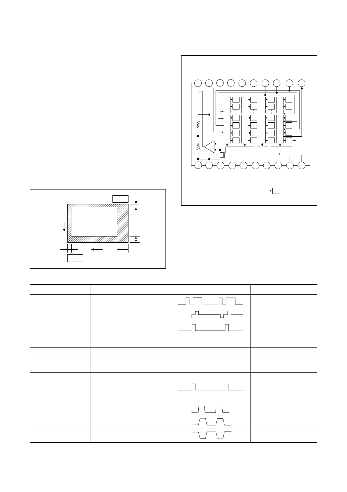
[1 ]CA1 CIRCUIT DESCRIPTION
1. IC Configuration
IC903 (ICX267) CCD imager
IC902, IC904, IC908 (74ACT04MTC) H driver
IC907 (CXD3400N) V driver
IC905 (AD9840) CDS, AGC, A/D converter
2. IC903 (CCD)
[Structure]
Interline type CCD image sensor
Optical size Diagonal 8 mm (1/2 type)
Effective pixels 1392 (H) X 1040 (V)
Pixels in total 1434 (H) X 1050 (V)
Actual pixels 1360 (H) X 1024 (V)
Optical black
Horizontal (H) direction: Front 2 pixels, Rear 40 pixels
Vertical (V) direction: Front 8 pixels, Rear 2 pixels
Dummy bit number Horizontal : 20 Vertical : 3
Pin 1
2
E-100RS
Fig. 1-2. CCD Block Diagram
V
2
Pin 11
Fig. 1-1.Optical Black Location (Top View)
Pin No.
1
2, 3
4
5, 6, 8,
14, 16
7, 9, 12
10
11
13
15
17
Symbol
Vφ
Vφ
2A, Vφ2B
Vφ3
NC
GND
VOUT
VDD
φSUB
CSUB
VL
1
8
H
40
Pin Description
Vertical register transfer clock
Vertical register transfer clock
Vertical register transfer clock
GND
Signal output
Circuit power
Substrate clock
Substrate bias
Protection transistor bias
Waveform
GND
DC
DC
DC
Voltage
-8.0 V, 0 V
-8.0 V, 0 V, 15 V
-8.0 V, 0 V
0 V
Aprox. 7 V
15 V
Different from every CCD
Different from every CCD
-8 V
18
19
20
φRG
Hφ
Hφ
Reset gate clock
1
2
Horizontal register transfer clock
Horizontal register transfer clock
12 V, 17 V
0 V, 5 V
0 V, 5 V
Table 1-1. CCD Pin Description
H-2 Ver.1SERVER_DIS
Page 3
DESCRIPTION OF MECHANISME-100RS
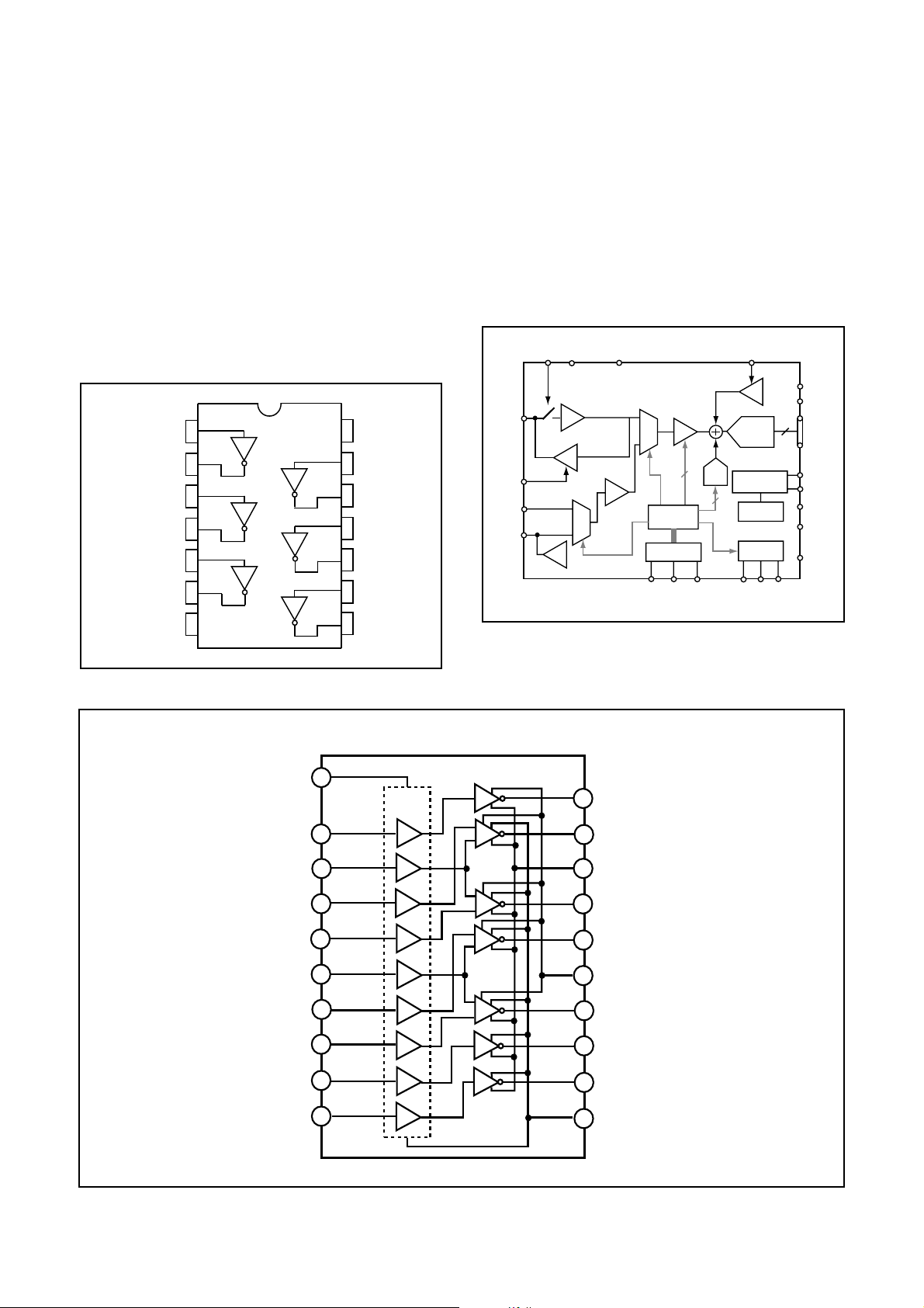
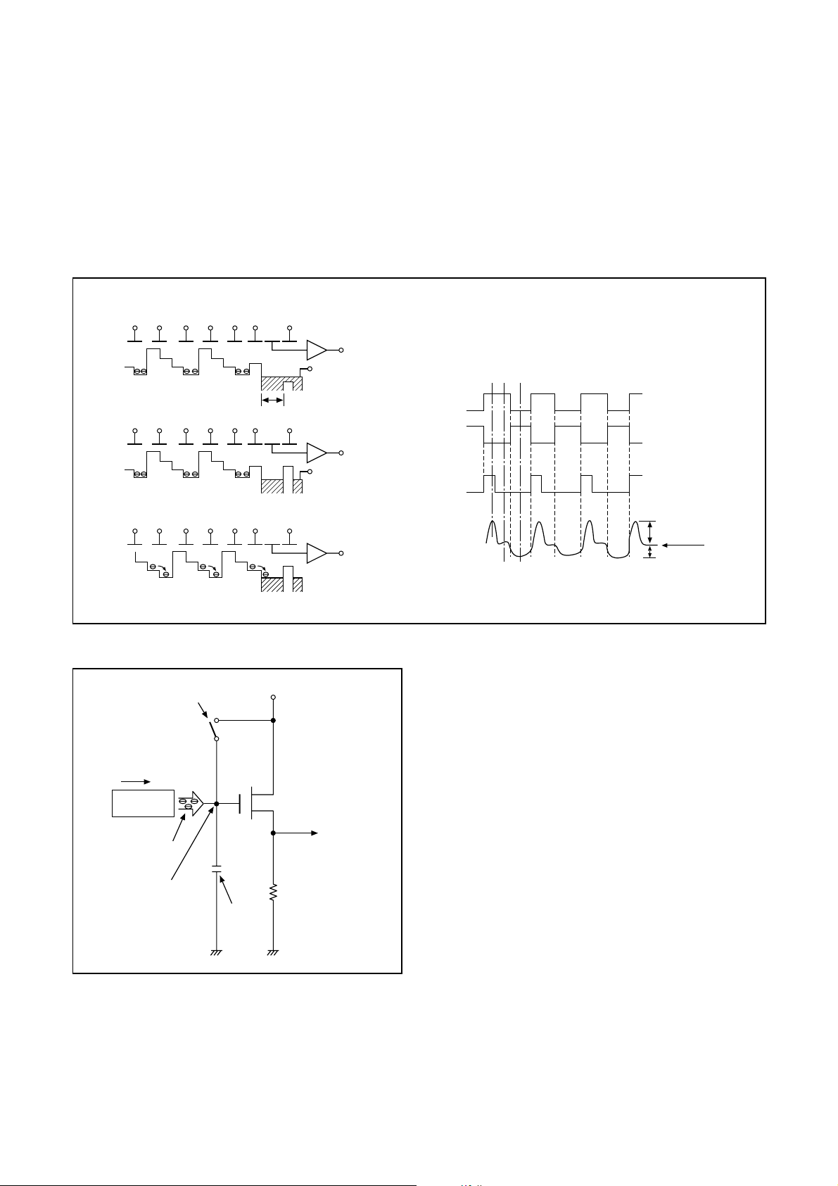
3. IC902, IC904, IC908 (H Driver) and IC907
(V Driver)
An H driver and V driver are necessary in order to generate the clocks (vertical transfer clock, horizontal transfer
clock and electronic shutter clock) which driver the CCD.
IC902, IC904 and IC908 are inverter IC which drives the
horizontal CCDs (H1 and H2). In addition the XV1-XV3 signals which are output from IC102 are the vertical transfer
clocks, and the XSG1 and XSG signal which is output from
IC102 is superimposed onto XV2A and XV2B at IC907 in
order to generate a ternary pulse. In addition, the XSUB
signal which is output from IC102 is used as the sweep
pulse for the electronic shutter, and the RG signal which is
output from IC102 is the reset gate clock.
14
CC
1A
1Y
2A
2Y
3A
3Y
GND
1
2
3
4
5
6
7
V
13
6A
12
6Y
11
5A
10
5Y
4A
9
4Y
8
4. IC905 (CDS, AGC Circuit and A/D Converter)
The video signal which is output from the CCD is input to
Pin (30) of IC905. There are S/H blocks inside IC905 generated from the XSHP and XSHD pulses, and it is here that
CDS (correlated double sampling) is carried out.
After passing through the CDS circuit, the signal passes
through the AGC amplifier. It is A/C converted internally
into a 10-bit signal, and is then input to IC102 of the CA2
circuit board. The gain of the AGC amplifier is controlled by
serial data which is output from IC102 of the CA2 circuit
board.
PBLK
CCDIN
CLPDM
AUX1IN
AUX2IN
AVDD
CDS
CLP
CLP
4 dB
MUX
AVSS
2~36 dB
2:1
VGA
MUX
10
BUF
2:1
CONTROL
REGISTERS
DIGITAL
INTERFACE
SCK
SL
SEN
SDATA
Offset
DAC
8
CLPOB
CLP
10-BIT
ADC
BANDGAP
REFERENCE
INTERNAL
INTERNAL
TIMING
Fig. 1-5. IC905 Block Diagram
AD9840
BIAS
DATA
SHDSHP
CLK
DRVDD
DRVSS
10
DOUT
VRT
VRB
CML
DVDD
DVSS
Fig. 1-3. IC902, IC904 and IC908 Block Diagram
V
DD
1
Input
Buffer
XSHT
2
XV2B
3
XSG2
4
NC
5
XV2A
6
NC
7
XSG1
8
XV1
9
XV3
10
SHT
V2B
V
NC
NC
V
V2A
V1
V3
GND
20
19
L
18
17
16
H
15
14
13
12
11
Fig. 1-4. IC907 Block Diagram
H-3Ver.1 SERVER_DIS
Page 4
H. DESCRIPTION OF MECHANISM
E-100RS
5. Transfer of Electric Charge by the Horizontal CCD
The transfer system for the horizontal CCD emplays a 2-phase drive method.
The electric charges sent to the final stage of the horizontal CCD are transferred to the floating diffusion, as shown in Fig. 1-
6. RG is turned on by the timing in (1), and the floating diffusion is charged to the potential of PD. The RG is turned off by the
timing in (2). In this condition, the floating diffusion is floated at high impedance. The H1 potential becomes shallow by the
timing in (3), and the electric charge now moves to the floating diffusion.
Here, the electric charges are converted into voltages at the rate of V = Q/C by the equivalent capacitance C of the floating
diffusion. RG is then turned on again by the timing in (1) when the H1 potential becomes deep.
Thus, the potential of the floating diffusion changes in proportion to the quantity of transferred electric charge, and becomes
CCD output after being received by the source follower. The equivalent circuit for the output circuit is shown in Fig. 1-7.
(1)
H1 H2 H1 H2 H1 HOG RG
CCD OUT
Floating diffusion
(2)
H1 H2 H1 H2 H1 HOG RG
PD
PD
CCD OUT
H1
H2
RG
15.5V
(1) (2) (3)
5.0V
0V
5.0V
0V
12V
(3)
H1 H2 H1 H2 H1 HOG RG
CCD OUT
Fig. 1-6. Horizontal Transfer of CCD Imager and Extraction of Signal Voltage
Reset gate pulse
Direction of transfer
H Register
Electric
charge
Floating diffusion gate is
floated at a high impedance
C is charged
equivalently
12V Pre-charge drain bias(PD)
Voltage output
Fig. 1-7. Theory of Signal Extraction Operation
6. Lens drive block
6-1. Shutter drive
The shutter drive signal (SHUTTER) which is output by the
ASIC and the aperture enable signal (AE SW) cause a positive and negative voltage are applied to the aperture drive
coil to open and close the lens aperture.
CCD OUT
RG pulse peak signal
Signal voltage
6-2. Iris drive
When in the aperture enable (AE SW) state, the target aperture value signal (IRIS PWM) which is output by the ASIC
and the aperture value signal (HALL OUT +/put by the lens are compared so that feedback control can
be carried out.
6-3. Focus drive
When the drive signals (FRSTB, FCW, FOEB and FCLK)
which are output from the ASIC, the focus stepping motor is
sine-wave driven by the micro-step motor driver (IC953). Detection of the standard focusing positions is carried out by
means of the photointerruptor (FOCUS PI) inside the lens
block.
6-4. Zoom drive
When the drive signals (ZRSTB, ZCW, ZOEB and ZCLK)
which are output from the ASIC, the zoom stepping motor is
sine-wave driven by the micro-step motor driver (IC954). Detection of the zoom positions is carried out by means of
photoreflector (ZOOM PI) inside the lens block.
H-4 Ver.1SERVER_DIS
Black level
) which is out-
Page 5

DESCRIPTION OF MECHANISME-100RS
[2] CA2 CIRCUIT DESCRIPTION
1. Circuit description
1-1. Digital clamp
The optical black section of the CCD extracts averaged values from the subsequent data to make the black level of
the CCD output data uniform for each line. The optical black
section of the CCD averaged value for each line is taken
as the sum of the value for the previous line multiplied by
the coefficient k and the value for the current line multiplied
by the coefficient 1-k.
1-2. Signal processor
γ γ
1.
γ correction circuit
γ γ
This circuit performs (gamma) correction in order to maintain a linear relationship between the light input to the camera and the light output from the picture screen.
2. Color generation circuit
This circuit converts the CCD data into RGB signals.
3. Matrix circuit
This circuit generates the Y signals, R-Y signals and B-Y
signals from the RGB signals.
4. Horizontal and vertical aperture circuit
This circuit is used gemerate the aperture signal.
1-3. AE/AWB and AF computing circuit
The AE/AWB carries out computation based on a 64-segment screen, and the AF carries out computations based
on a 6-segment screen.
1-4. SDRAM controller
This circuit outputs address, RAS, CAS and AS data for
controlling the SDRAM. It also refreshes the SDRAM.
1-5. Communication control
1. SIO
This is the interface for the 8-bit microprocessor.
2. PIO/PWM/SIO for LCD
8-bit parallel input and output makes it possible to switch
between individual input/output and PWM input/output.
1-6. TG/SG
Timing generated for 2 million pixel CCD control.
1-7. Digital encorder
It generates chroma signal from color difference signal.
2. Outline of Operation
When the shutter opens, the reset signals, TEST0, TEST1
signals (ASIC and CPU) and the serial signals (“take a picture” commands) from the 8-bit microprocessor are input
and operation starts. When the TG/SG drives the CCD, picture data passes through the A/D and CDS, and is then
input to the ASIC as 10-bit data. This data then passes
through the DCLP, AWB, shutter and
is input to the SDRAM. The AF, AE, AWB, shutter, and AGC
value are computed from this data, and three exposures
are made to obtain the optimum picture. The data which
has already been stored in the SDRAM is read by the CPU
and interpolating pixel is carried out. Each pixel is interpolated from the surrounding data as being either R, G or B
primary color data to produce R, G and B data. At this time,
correction of the lens distortion which is a characteristic of
wide-angle lenses is carried out. Aperture correction is
carried out. If the data is a still picture, it is compressed
into JPEG format, and if the data is a moving picture, it is
compressed into MJPEG format. The data is then written
to the compact flash card or to the Smart Media card. When
the data is to be output to an external device, it is taken
data from the memory and output via the USB. When played
back on the LCD and monitor, data is transferred from
memery to the SDRAM, and the image is then elongated
so that it is displayed over the SDRAM display area.
γγ
γ
circuit, after which it
γγ
3. LCD Block
During monitoring, YUV conversion is carried out for the 10bit CCD data which is input from the A/D conversion block to
the ASIC and is then transferred to the DRAM so that the
CCD data can be displayed on the LCD.
The data which has accumulated in the DRAM is passed
through the NTSC encoder , and after D/A conversion is carried out to change the data into a Y/C signal, the data is sent
to the LCD panel and displayed.
If the shutter button is pressed in this condition, the 10-bit
data which is output from the A/D conversion block of the
CCD is sent to the DRAM (DMA transfer), and after processor, it is displayed on the LCD as a freeze-frame image.
During playback, the JPEG image data which has accumulated in the flash memory is converted to YUV signals, and
then in the same way as during monitoring, it is passed through
the NTSC endoder, and after D/A conversion is carried out to
change the data into a Y/C signal, the data is sent to the LCD
panel and displayed.
The two analog signal (Y/C signals) from the ASIC are converted into RGB signals by the LCD driver, and these RGB
signals and the control signal which is output by the LCD driver
are used to drive the LCD panel. The RGB signals are 1H
transposed so that no DC component is present in the LCD
element, and the two horizontal shift register clocks drive the
horizontal shift registers inside the LCD panel so that the 1H
transposed RGB signals are applied to the LCD panel. Because the LCD closes more as the difference in potential between the COM (common polar voltage: fixed at DC) and the
R, G and B signals becomes greater, the display becomes
darker; if the difference in potential is smaller, the element
opens and the LCD become brighter.
H-5Ver.1 SERVER_DIS
Page 6

H. DESCRIPTION OF MECHANISM
[3] TC2/CA3 CIRCUIT DESCRIPTION
1. Configuration
For the overall configuration of the TC2 and CA3 circuit
boards, refer to the block diagram. The configuration of the
TC2 circuit board centers around a 16-bit microprocessor
(IC702). The configuration of the CA3 ciurcuit board centers two gyro sensors. (S7501, S7502)
2. Picture Stabilizer Function
The picture stabilizer system comprises both the CA3 circuit board and the TC2 circuit board. Firstly, the two gyroscope sensors on the CA3 circuit board sense if there is
any vibration in the horizontal and vertical directions, and
the resulting data is sent to the TC2 circuit board. The 16bit microprocessor on the TC2 circuit board reads the data
on camera vibration from the gyroscope sensors (CA3 circuit board), as well as the lens position data (zoom position
and focus position) from the camera circuit (ASIC) and the
data for the current shift lens position (the amount of optical correction from the actual position) from the lens, and
outputs the shift lens movement data for obtaining the optimum level of correction. This output data is converted by
the D/A converter into an analog signal which is then input
to the analog circuit for controlling the shift lens, where it is
used to adjust the lens.
E-100RS
H-6 Ver.1SERVER_DIS
Page 7

DESCRIPTION OF MECHANISME-100RS
[4] PW1 POWER CIRCUIT DESCRIPTION
1. Outline
This is the main power circuit, and is comprised of the following blocks.
Switching controller (IC501)
Switching controller (IC502)
Analog system power output (T5001, Q5002)
Digital 2.55 V system power output (Q5007)
Digital 3.40 V system power output (Q5018)
LCD system power output (Q5001, T5002)
LCD backlight power supply output (Q5032, T5003)
Digital 5.25 V and Analog 5.1 V system power output
(Q5026, Q5009)
Picture stabilizer control 5 V and lens drive 5 V power output (Q5027)
EVF backlight power output (IC503)
2. Switching Controller (IC501)
This is the basic circuit which is necessary for controlling
the power supply for a PWM-type switching regulator, and
is provided with four built-in channels, only CH1 (analog
system), CH3 (LCD system), CH2 (digital 2.55 V) and CH4
(digital 3.40 V) are used. Feedback from 15.2 V (A) (CH1),
2.55 V (D) (CH2) , 13.0 V (L) (CH3) and 3.40 V (D) (CH4)
power supply outputs are received, and the PWM duty is
varied so that each one is maintained at the correct voltage
setting level.
5. Digital 2.55 V System Power Output
2.55 V (D) is output. Feedback is provided to the swiching
controller (Pin (26) of IC501) so that PWM control can be
carried out.
6. Digital 3.40 V System Power Output
3.40 V (D) is output. Feedback is provided to the swiching
controller (Pin (7) of IC501) so that PWM control can be
carried out.
7. LCD System Power Output
13.0 V (L) and 15.5 V (L) are output. Feedback for the 13.0
V (L) is provided to the switching controller (Pin (11) of
IC501) so that PWM control can be carried out. In addition,
when the EVF is illuminated, (and thus the LCD is switched
off), 12.4 V (F) is output by this system.
8. LCD Backlight Power Supply output
7 V (L) is output. Feedback is sent to pins (11) of the switching controller (IC502) for PWM control to be carried out.
9. Inverter Control
The LCD backlight uses a 1.8-inch flat picture tube, and is
illuminated by controlling T5003 with pulses which are driven
by the inverter clock.
fH
2-1. Short-circuit protection circuit
If output is short-circuited for the length of time determined
by the condenser which is connected to Pin (17) of IC501,
all of IC501 output is turned off. The control signal (P ON,
P(A) ON and LCD ON) are recontrolled to restore output.
3. Switching Controller (IC502)
This is the basic circuit which is necessary for controlling
the power supply for a PWM-type switching regulator, and
is provided with four built-in channels, only CH1 (picture
stabilizer control 5 V and lens drive 5 V system), CH2 (digital 5.25 V and analog 5.1 V), CH3 (LCD backlight system)
and CH4 (5.7 V system). Feedback from 5 V (T) (CH1),
5.25 V (D) (CH2), 7.0 V (L) (CH3) and 5.7 V (CH4) power
supply outputs are received, and the PWM duty is varied
so that each one is maintained at the correct voltage setting level.
3-1. Short-circuit protection circuit
If output is short-circuited for the length of time determined
by the condenser which is connected to Pin (17) of IC502,
all of IC502 output is turned off. The control signal (P ON,
P(A) ON and LCD ON) are recontrolled to restore output.
4. Analog System Power Output
15.2 V (A), -8.1 V (A) and 3.85 V (A) are output. Feedback
for the 15.2 V (A) is provided to the switching controller
(Pins (29) of IC501) so that PWM control can be carried
out.
Inverter clock
3 seconds for illumination 5.6 µs
3 seconds after illumination 5.4 µs
10. Digital 5.25 V and Analog 5.1 V Power Output
5.25 V (D) and 5.1 V (A) are output. Feedback for the 5.25
V (D) is provided to the switching controller (Pins (26) of
IC502) so that PWM control can be carried out.
11. Picture Stabilizer Control 5 V and Lens Drive 5
V Power Output
5 V (T) and 5 V (M) are output. Feedback is provided to the
switching controller (Pins (29) of IC502) so that PWM control can be carried out.
12. EVF Backlight Power Output
15 mA (F) is output. Constant current operation is used so
that the current flowing to the backlight (white LED) is 15
mA. This is controlled by IC503.
13. Temperature Sensor
The temperature of the inverter transformer T5003 is detected, and a voltage which corresponds to the detected
temperature is output to the 8-bit microprocessor IC301. If
T5003 becomes abnormally hot, causing the above voltage to increase past a certain level, the mode then switches
to sleep mode.
H-7Ver.1 SERVER_DIS
Page 8

H. DESCRIPTION OF MECHANISM
[5] PW1 STROBE CIRCUIT DESCRIPTION
E-100RS
1. Charging Circuit
When UNREG power is supplied to the charge circuit and
the CHG signal becomes High (3.3 V), the charging circuit
starts operating and the main electorolytic capacitor is
charged with high-voltage direct current.
However, when the CHG signal is Low (0 V), the charging
circuit does not operate.
1-1. Power switch
When the CHG signal switches to Hi, Q5406 turns ON and
the charging circuit starts operating.
1-2. Power supply filter
L5401 and C5401 constitute the power supply filter. They
smooth out ripples in the current which accompany the
switching of the oscillation transformer.
1-3. Oscillation circuit
This circuit generates an AC voltage (pulse) in order to increase the UNREG power supply voltage when drops in
current occur. This circuit generates a drive pulse with a
frequency of approximately 50-100 kHz. Because self-excited light omission is used, the oscillation frequency
changes according to the drive conditions.
2. Light Emission Circuit
When RDY and TRIG signals are input from the ASIC expansion port, the stroboscope emits light.
2-1. Emission control circuit
When the RDY signal is input to the emission control circuit, Q5409 switches on and preparation is made to let current flow to the light emitting element. Moreover, when a
STOP signal is input, the stroboscope stops emitting light.
2-2. Trigger circuit
When a TRIG signal is input to the trigger circuit, D5405
switches on, a high-voltage pulse of several kilovolts is generated inside the trigger circuit, and this pulse is then applied to the light emitting part.
2-3. Light emitting element
When the high-voltage pulse form the trigger circuit is applied to the light emitting part, currnet flows to the light emitting element and light is emitted.
Beware of electric shocks.
1-4. Oscillation transformer
The low-voltage alternating current which is generated by
the oscillation control circuit is converted to a high-voltage
alternating current by the oscillation transformer.
1-5. Rectifier circuit
The high-voltage alternating current which is generated at
the secondary side of T5401 is rectified to produce a highvoltage direct current and is accumulated at electrolytic capacitor C5412 on the main circuit board.
1-6. Voltage monitoring circuit
This circuit is used to maintain the voltage accumulated at
C5412 at a constance level.
After the charging voltage is divided and converted to a
lower voltage by R5417 and R5419, it is output to the SY1
circuit board as the monitoring voltage VMONIT. When this
VMONIT voltage reaches a specified level at the SY1 circuit board, the CHG signal is switched to Low and charging
is interrupted.
H-8 Ver.1SERVER_DIS
Page 9

DESCRIPTION OF MECHANISME-100RS
[6] SY1 CIRCUIT DESCRIPTION
1. Configuration and Functions
For the overall configuration of the SY1 circuit board, refer to the block diagram. The configuration of the SY1 circuit board
centers around a 8-bit microprocessor (IC301).
The 8-bit microprocessor handles the following functions.
1. Operation key input, 2. Mode LCD display, 3. Clock control, 4. Power ON/OFF, 5. Storobe charge control
Pin
1
2
3
4~7 SCAN IN 0~3
8
9
10
11
12
13~19
20
21
22
23~26
27
28~30
31
32~47
48~55
56
57 CARD SW
58 CF_CARD
59 SELF LED
60 AF LED
61~63 SCAN IN 4~6
64 NOT USED - -
65 D_LED ON I Card LED control signal H : LED light
66 EVF ON
67 MIC JACK
68 AD_RST O CDS/ADC IC control signal
69 BACKUP CTL
70
71
72
73
74
75
76
77
78
79
80
Signal
CHG VOL
TEMP_SENS
SCAN OUT 4
AVDD
AVREF
CARD LED
NOT USED
VSS
NOT USED
AVREF ON
NOT USED
CHG ON
COM0~COM3
BIAS
VLC0~VLC2
VSS
S1~S16
NOT USED
EVF BL
PA ON
P ON
NOT USED
CARD
AV JACK
SI
SO
SCK
IC
XOUT
XIN
I/O
I
I
O
I
-
I
O
-
-
-
O
-
O
O
-
-
-
O
-
O EVF backlight ON/OFF signal H : ON
I
I
O AF LED luminous control signal (SELF) L : ON
O AF LED luminous control signal L : ON
I
O
I External microphone input cable connection detection signal H : Connection
O
O
O
-
I
I
I
O
O
-
O
I
Strobe charge voltage input (analog input)
Inverter transfer (PW1) temparature detection (analog input)
Key matrix output
Key matrix input
A/D converter analog power terminal
A/D converter standard voltage input terminal
Card LED L : LED light
-
GND
-
A/D standard voltage ON/OFF signal L : ON
-
Flash charge ON/OFF signal H : ON
Mode LCD common signal output
LCD motor voltage supply terminal
LCD motor voltage terminal
GND
Mode LCD segment signal output
-
Card lid switch input terminal L : close H : open
Extension memory card attachment detection signal (CF) L : Attachment
Key matrix input
EVF monitor power ON/OFF signal H : ON
Lithum second battery charge control signal
DC/DC converter (analog) ON/OFF signal H : ON
DC/DC converter ON/OFF signal H : ON
-
Extension memory card attachment detection signal (smart media) L : Attachment
Video output cable connection detection signal H : Connection
Serial communication data input (←ASIC)
Serial communication data output (→ASIC)
Serial communication clock output (→ASIC)
Connect to VSS
Main clock oscillation terminal (4 MHz)
Main clock oscillation terminal
Outline
See next page →
H-9Ver.1 SERVER_DIS
Page 10

81
82
83
84
85
86
87
88
89
90
91~94
95
96
97
98
99
100
VDD
XCIN
XCOUT
RESET
BAT OFF
NOT USED
SREQ
IR IN
STR CONNECT
USB
SCAN OUT 0~3
LCD ON
ASIC TEST
ASIC RESET
MAIN RESET
AVSS
BATTERY
H. DESCRIPTION OF MECHANISM
-
I
O
I
I
-
I
I
I
I
O
O
O
O
O
-
I
Table 4-1. 8-bit Microprocessor Port Specification
Power supply terminal
Sub clock oscillation terminal (32.768 kHz)
Sub clock oscillation terminal
Reset input
Battery OFF detection signal L : OFF
-
Serial communication request signal L : Request
IR remote control signal input terminal
External strobo detection signal
USB connector connection detection signal L : Connection
Key matrix output
LCD monitor power ON/OFF signal H : ON
ASIC reset control signal
ASIC reset signal L : Reset output
SPARC reset signal L : Reset output
A/D converter GND power terminal
Battery voltage input (analog input)
E-100RS
2. Internal Communication Bus
The SY1 circuit board carries out overall control of camera operation by detecting the input from the keyboard and the
condition of the camera circuits. The 8-bit microprocessor reads the signals from each sensor element as input data and
outputs this data to the camera circuits (ASIC) or to the LCD display device as operation mode setting data. Fig. 4-1 shows
the internal communication between the 8-bit microprocessor and ASIC RISC CPU circuits.
RESET
SREQ
8-bit
Microprocessor
Fig. 4-1 Internal Bus Communication System
ASIC SO
ASIC SI
ASIC SCK
RESET
3. Key Operaiton
For details of the key operation, refer to the instruction manual.
SCAN
SCAN
OUT
IN
0
1
0
DR
OK
1
SPT
MO
23
MC
MN
AEL
P OFF
ASIC RISC CPU
1 CHIP CPU
4
External release
wire 1st
P ON
5
External release
wire 2nd
RESET
6
TEST
2
3
4
J UP
Z D1
SEQUENTIAL
SHOT
J DOWN
Z D2
IS
J LEFT
Z UP2
M
Table 4-2. Key Matrix table
J RIGHT
Z UP2
SA
IF
1st
FL
2nd
P
HOP UP SW
BATTERY
PLAY
H-10 Ver.1SERVER_DIS
Page 11

DESCRIPTION OF MECHANISME-100RS
4. Power Supply Control
The 8-bit microprocessor controls the power supply for the overall system.
The following is a description of how the power supply is turned on and off. When the battery is attached, a regulated 3.2 V
voltage is normally input to the 8-bit microprocessor (IC301) by IC302, so that clock counting and key scanning is carried out
even when the power switch is turned off, so that the camera can start up again. When the battery is removed, the 8-bit
microprocessor operates in sleep mode using the backup battery. At this time, the 8-bit microprocessor only carries out clock
counting, and waits in standby for the battery to be attached again. When a switch is operated, the 4-bit microprocessor
supplies power to the system as required.
The 8-bit microprocessor first sets both the P ON signal at pin (71) and the PA ON signal at pin (70) to high, and then turns
on the DC/DC converter. After this, High signals are output from pins (97) and (88) so that the ASIC RISC CPU is set to the
active condition. If the LCD monitor is on, the LCD ON signal at pin (95) set to high, and the DC/DC converter for the LCD
monitor is turned on. Once RISC CPU processing is completed, the ASIC RISC CPU return to the reset condition, all DC/DC
converters are turned off and the power supply to the whole system is halted.
Power
ON
Supply voltage
Power OFF
Play back
Power switch ON-Auto power down
Shutter switch ON
Resolution, Flash, Self timer switch ON
LCD finder
Table 4-3. Camera Mode (Battery Operation)
Supply voltage
ASIC, RISC
CPU,
memory
3.3 V, 2.5 V
OFF
ON
OFF
ON
OFF
ON
ASIC, RISC
CPU,
memory
3.3 V
CCD
5 V (A)
+15 V -8 V
OFF
OFF
OFF
ON→OFF
OFF
ON
CCD
5 V (A)
+15 V -8 V
4bit
CPU
3.2 V
(ALWAYS)
32KHz OFF OFF
4MHz ON ON/OFF
4MHz ON OFF
4MHz ON OFF
4MHz ON OFF
4MHz ON ON/OFF
4bit
CPU
3.2 V
(ALWAYS)
MODE
LCD
3.2 V
(ALWAYS)
MODE
LCD
3.2 V
(ALWAYS)
LCD (EVF)
MONITOR
5V (L)
+12V etc.
LCD (EVF)
MONITOR
5 V (L)
+12V etc.
Power OFF
Power switch ON-Auto power down
Take a picture
Power
ON
Note) P. SAVE = Power save mode, 4 MHz = Main clock operation, 32 kHz = Sub clock operation
Erase image
Download image
Continuous image
Message from host
Table 4-4. Host Mode (Battery Operation)
OFF
OFF
ON
ON
ON
ON
ON
OFF
OFF
ON→OFF
OFF
OFF
ON
ON
32 KHz OFF OFF
4 MHz ON OFF
4 MHz ON OFF
4 MHz ON OFF
4 MHz ON OFF
4 MHz ON OFF
4 MHz ON OFF
H-11Ver.1 SERVER_DIS
 Loading...