

E2D0026-27-43
This version: Jan. 1998
¡ Semiconductor
Previous version: May. 1997
MSM6688/6688L
ADPCM Solid-State Recorder IC
GENERAL DESCRIPTION
The MSM6688/6688L is a “solid-state recorder” IC developed using the ADPCM method. By
externally connecting a microphone, a speaker, a speaker drive amplifier, and a dedicated register
to store ADPCM data, it can record and play back voice data in a manner similar to a tape recorder.
The MSM6688 supports 5 V operation and has a stand-alone mode and a microcontroller interface
mode.
The MSM6688L supports 3 V operation and controls recording/playback in microcontroller interface
mode.
In the stand-alone mode, recording/playback conditions can be selected by pins and the MSM6688/
6688L can be controlled by a simple drive timing. In the microcontroller interface mode, recording/
playback can be controlled by commands from the microcontroller. In the microcontroller interface
mode, the MSM6688/6688L is much more flexible than in the stand-alone mode.
In addition, the MSM6688/6688L can form easily a recording and playback circuit with fixed
messages by connecting serial registers and serial voice ROMs as external memories.
Note: This data sheet explains a stand-alone mode and a microcontroller interface mode, separately.
Differences Between MSM6688 and MSM6688L
Parameter MSM6688 MSM6688L
Operating voltage 3.5 to 5.5 V 2.7 to 3.6 V
Control mode Standalone mode,
Microcontroller interface mode
Full scale of A/D and D/A
converters
Voice detection level for voice
triggered starting
External-only register 32M bits (max.)
±
0 to V
DD
V
DD
64
4M bits (MSM6684B)
8M bits (MSM6685)
, ±
V
DD
, ±
32
V
DD
16
Microcontroller interface
mode only
1
VDD to
4
V
DD
±
128
4M bits (max.)
4M bits (MSM66V84B)
, ±
3
V
DD
4
V
DD
64
, ±
V
DD
32
1/159

¡ Semiconductor MSM6688/6688L
CONTENTS
(1) STAND-ALONE MODE
(for MSM6688 (5 V Version))
FEATURES ........................................................ 3
BLOCK DIAGRAM .......................................... 4
PIN CONFIGURATION..................................5
PIN DESCRIPTIONS .......................................6
ABSOLUTE MAXIMUM RATINGS ............ 10
RECOMMENDED OPERATING
CONDITIONS ................................................. 10
ELECTRICAL CHARACTERISTICS ...........11
TIMING DIAGRAMS .................................... 15
FUNCTIONAL DESCRIPTION ...................28
Recording Time and Memory
Capacity ................................................28
Connection of an Oscillator.....................28
Power Supply Wiring...............................29
Analog Input Amplifier Circuit ............. 29
Connection of LPF Circuit
Peripherals ...........................................30
LPF Characteristics ...................................31
Reset Function ...........................................32
Power Down by the PDWN pin .............33
Record/Playback Control Mode ............34
Deleting phrases .......................................36
Recording Method .................................... 37
Playback Method ...................................... 38
ROM Playback Method............................39
Voice Triggered Starting..........................40
Method of Temporarily Stopping Record/
Playback by Pause Function ..............
APPLICATION CIRCUIT .............................43
42
(2) MICROCONTROLLER INTERFACE
MODE
(for MSM6688 (5 V Version)
and MSM6688L (3 V Version))
FEATURES ....................................................... 44
BLOCK DIAGRAM ......................................... 45
PIN CONFIGURATION................................. 46
PIN DESCRIPTIONS ...................................... 47
ABSOLUTE MAXIMUM RATINGS
(for MSM6688 (5 V Version)) ......................... 50
RECOMMENDED OPERATING CON-
DITIONS (for MSM6688 (5 V Version)) ....... 50
ELECTRICAL CHARACTERISTICS
(for MSM6688 (5 V Version)) ......................... 50
ABSOLUTE MAXIMUM RATINGS
(for MSM6688L (3 V Version)) ...................... 55
RECOMMENDED OPERATING CONDITIONS
(for MSM6688L (3 V Version)) ...................... 55
ELECTRICAL CHARACTERISTICS
(for MSM6688L (3 V Version)) ...................... 55
TIMING DIAGRAMS ..................................... 60
FUNCTIONAL DESCRIPTION .................... 79
Recording Time and Memory
Capacity .................................................79
Connection of an Oscillator...................... 79
Power Supply Wiring................................ 81
Analog Input Amplifier Circuit .............. 81
Connection of LPF Circuit
Peripherals ............................................ 82
LPF Characteristics .................................... 82
Full Scale of A/D and D/A Converters . 83
Reset Function ............................................84
Power Down by the PDWN pin .............. 85
Record/Playback Control Modes ........... 86
Data Configuration of External Serial
Registers ................................................ 88
Data Configuration of External
Serial Voice ROMs ............................... 97
Command Description.............................. 99
Status Register .......................................... 108
Inputting the Commands ....................... 112
Changes of Record/Playback
Conditions ...........................................116
Setting and Confirming the
Record/Playback Conditions ................ 117
Flex Record/Playback Method.............. 128
Direct Record/Playback Method .........135
ROM Playback by Inputting Address
Code ..................................................... 138
Direct ROM Playback Method............... 142
Stopping Record/
Playback Temporarily ....................... 144
Transferring Data to/from External
Memories ............................................. 145
Record/playback by Inputting/
Outputting Voice Data via Data Bus ........
Suppression of Pop Noise at
AOUT Output ..................................... 155
APPLICATION CIRCUIT ............................ 157
151
2/159

¡ Semiconductor MSM6688/6688L
(1) STAND-ALONE MODE (for MSM6688 (5 V Version))
FEATURES
• 3-bit or 4-bit ADPCM
• Built-in 12-bit AD converter
• Built-in12-bit DA converter
• Built-in microphone amplifier
• Built-in low-pass filter
Attenuation characteristics –40 dB/oct
• External memories
Serial registers, 32M bits maximum (for variable messages)
8M bit serial register (MSM6685) can be driven directly
Serial voice ROMs, 4M bits maximum (for fixed messages)
1M bit serial voice ROM (MSM6595A) can be driven directly
2M bit serial voice ROM (MSM6596A) can be driven directly
3M bit serial voice ROM (MSM6597A) can be driven directly
• Sampling frequency
4.0 kHz, 5.3 kHz, 6.4 kHz or 8.0 kHz (master clock frequency = 4.096 MHz)
8.0 kHz, 10.6 kHz, 12.8 kHz, or 16.0 kHz (master clock frequency = 8.192 MHz)
• Number of phrases
63 phrases for variable messages
63 phrases for fixed messages
• Maximum recording time (when external 32M bit RAM is connected)
34 minutes (for 16 kbps ADPCM)
23 minutes (for 24 kbps ADPCM)
17 minutes (for 32 kbps ADPCM)
• Voice triggered starting function
• Pause function
• Master clock frequency: 4.096 MHz~8.192 MHz
• Power supply voltage: Single 5 V power supply
• Package:
56-pin plastic QFP (QFP56-P-910-0.65-2K) (Product name: MSM6688GS-2K)
3/159
4/159
¡ Semiconductor MSM6688/6688L
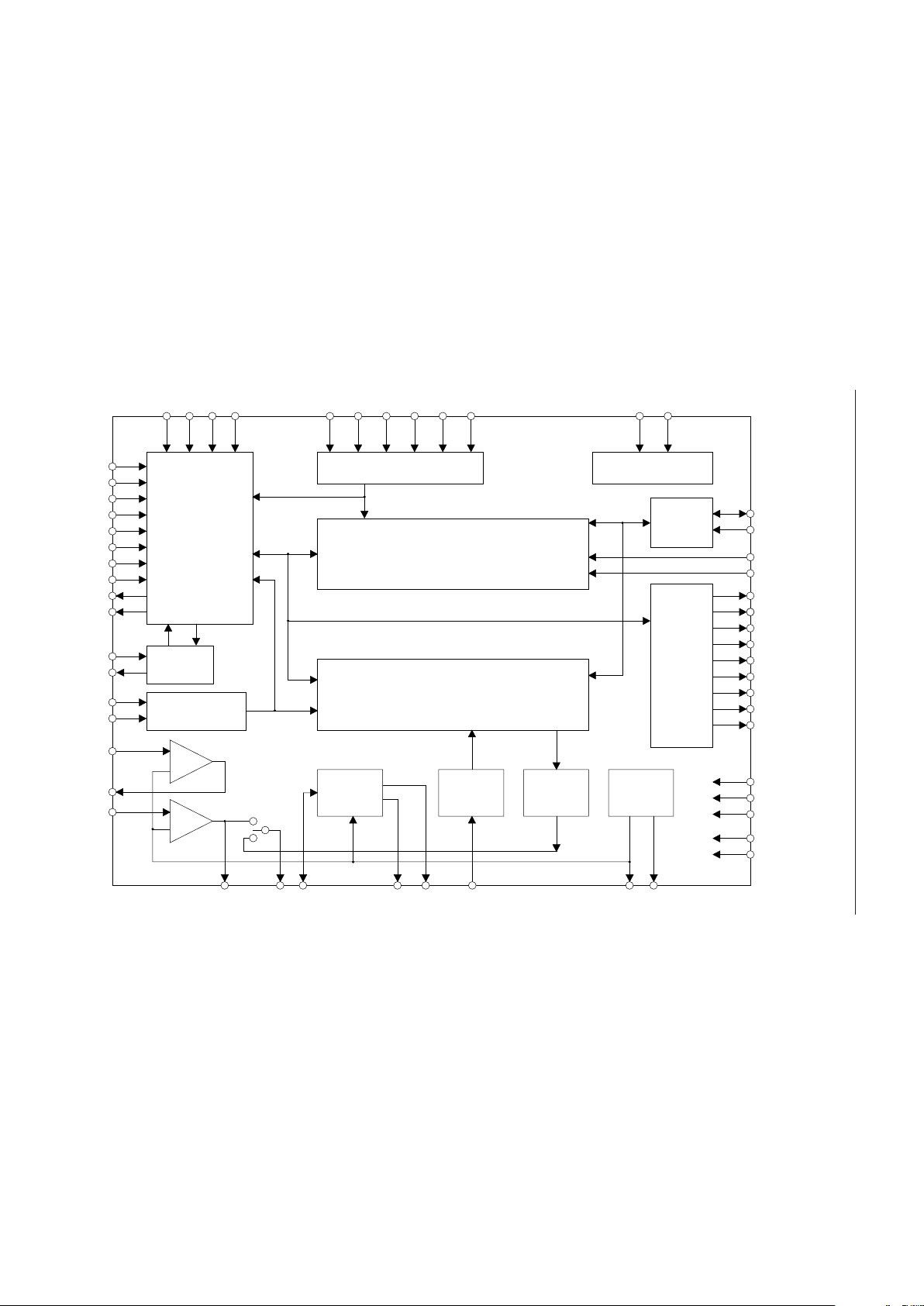
BLOCK DIAGRAM
MCUM
RESET
PDWN
PDMD
VDS
ROM
SAM1
SAM2
MON
NAR
DEL ST SP PAUSE CA0 CA1 CA2 CA3 CA4 CA5
TESTTEST
XT
XT
REC/PLAY
4B/3B
MIN
MOUT
LIN
OSC
Latch
–
+
–
+
LOUT AMON FIN AOUT FOUT ADIN SG SGC
SADX
SADY
TAS
RWCK
WE
CS1
CS2
CS3
CS4
RSEL1
RSEL2
DI/O
DROM
Test Circuit
Data
I/O
Register
Controller
ADPCM
Analyzer/Synthesizer
LPF
12bit
ADC
12bit
DAC
SG
Circuit
DV
DD
DV
DD'
AV
DD
DGND
AGND
Phrase Register
Address Controller
Timing
Controller
¡ Semiconductor MSM6688/6688L
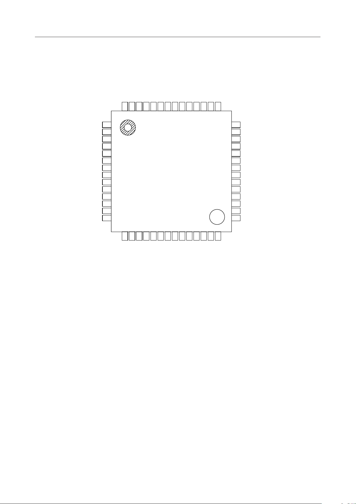
PIN CONFIGURATION (TOP VIEW)
CA0
CA1
CA2
CA3
CA4
CA5
DEL
PAUSE
PDMD
MCUM
SAM1
SAM2
4B/3B
VDS
10
11
12
13
14
REC/PLAYSTSP
56555453525150494847464544
1
2
3
4
5
6
7
8
9
15161718192021222324252627
ROM
ADIN
FOUT
RESET
NAR
FIN
AOUT
MON
RWCK
DD'
AMON
DV
DVDDXTXTWE
SG
DD
SGC
AV
LOUT
DROM
DI/0
LIN
MOUT
CS4
43
28
MIN
42
41
40
39
38
37
36
35
34
33
32
31
30
29
CS3
CS2
CS1
SADX
SADY
TAS
SAS
PDWN
TEST
TEST
RSEL2
RSEL1
DGND
AGND
56-Pin Plastic QFP
5/159

¡ Semiconductor MSM6688/6688L
PIN DESCRIPTIONS
Pin
49
21
22
30
29
23
24
28
26
27
25
20
19
17
16
18
39
38
36
37
Symbol Type Description
Digital power supply pin. Insert a bypass capacitor of 0.1µF or more
DV
DV
DD
DD'
—
between this pin and the DGND pin.
— Digital power supply pin
Analog power supply pin. Insert a bypass capacitor of 0.1µF or more
AV
DD
—
between this pin and the AGND pin.
DGND — Digital ground pin
AGND — Analog ground pin
SG
SGC
MIN
LIN
MOUT
LOUT
O
O
Output pin for analog circuit reference voltage (signal ground)
Inverting input pin of the built-in OP amplifier. Non-inverting input
I
pin is internally connected to SG (signal ground).
MOUT and LOUT are output pins of the built-in OP amplifier for MIN
and LIN, respectively.
This pin is connected to the LOUT pin in the recording mode and to
AMON O
the DA converter output in the playback mode. Used to connect the
built-in LPF input (FIN pin).
FIN I Input pin of the built-in LPF.
Output pin of the built-in LPF. Used to connect the AD converter
FOUT O
input (ADIN pin).
ADIN I Input pin of the built-in 12-bit AD converter.
Output pin of the built-in LPF. This pin outputs playback waveforms
AOUT O
and used to connect an external speaker drive amplifier.
(Serial Address Data). SADX is used to connect the SAD pin of each
SADX
SADY
O
external serial register and the SADX pin of each external serial voice
ROM. SADY is used to connect the SADY pin of each external serial
voice ROM. Outputs of starting address of read/write.
(Serial Address Strobe). Used to connect the SAS pin of external
SAS O
serial register and the SASX and SASY pins of
external serial voice ROM. Clock pin to write the serial address.
(Transfer Address Strobe). Used to connect the TAS pin of each
external serial register and serial voice ROM.
TAS O
This pin outputs address strobe outputs to set the serial address
data from the SADX and SADY pins into the internal address counter
of each serial register and serial voice ROM.
50
46
RWCK O
WE O
(Read/Write Clock). Used to connect the RWCK pin of each external
serial register and the RDCK pin of each external
serial voice ROM. This pin outputs a clock to read data from or write
it into each external serial register.
(Write Enable) Used to connect the WE pin of each external
serial register. This pin outputs WE signal to
select either read or write mode.
6/159
¡ Semiconductor MSM6688/6688L
Pin
45
40
41
42
43
31
32
10
53
35
Symbol Type Description
(Data I/O). Used to connect the DIN and DOUT pins of serial register.
DI/O44
DROM
CS1
CS2
CS3
CS4
RSEL1
RSEL2
MCUM I
RESET I
PDWN I
I/O
O
This pin outputs the data to be written into the serial register or
inputs the data read from the serial registers.
(Data ROM). Used to connect the DOUT pin of each external serial
I
voic ROM.
(Chip Select). Used to connect the CS pin of serial register and the
CS (CS1, CS2, CS3) pins of serial voice ROM.
(Register Select). These are used to select the number of external
serial registers.
I
RSEL2 L L H H
RSEL1 L H L H
Number of serial registers 1234
This pin is used to select either the stand-alone mode or the
microcontroller interface mode.
Low level: Stand-alone mode
High level: Microcontroller interface mode.
A high input level to this pin causes the MSM6688 to be initialized
and to go into the power down state.
(Power Down). When a low level is input to this pin, the MSM6688
goes to the power down state. Unlike the RESET pin, this pin does
not force to reset the MSM6688. When an Low level is applied to
this PDWN pin during recording operation, the MSM6688 is halted,
and will be maintained in the power down state while PDWN is low.
After this pin is restored to a high level, postprocessing for
recording will be performed.
47
48
34
33
XT I
XT O
TEST
TEST
Used to connect an oscillator. When an external clock is used,
input the clock through this pin. At the power down state, this pin
must be set to the ground level.
Used to connect an oscillator, when an external clock is used, this
pin must be left open.
I
Used to test the MSM6688. Input a low level to the TEST pin and
a high level to the TEST pin.
7/159
¡ Semiconductor MSM6688/6688L
Pin
15
56
55
54
8
7
TypeSymbol Description
ROM I
REC/PLAY I
ST I
SP I
PAUSE I
DEL I
When low, selects the record/playback operation. When high, selects the ROM
playback operation.
Used to select the recording mode or the playback mode. This pin is invalid
during the ROM playback operation. When low, selects the playback mode.
When high, selects the recording mode.
When a low-level pulse is applied to this pin, the record/playback or ROM
playback is started.
When a low-level pulse is applied to this pin, the record/playback or ROM
playback is stopped.
When a low-level pulse is applied to this pin, the record/playback or ROM
operation is stopped temporarily.
When a low level pulse is applied to this pin, all phase deletion or specified
phrase deletion can be performed according to the setting of pins CA0
through CA5,
ch00: All phase deletion
ch01 to ch3F: Specified phrase deletion
After powering up, be sure to input RESET signal and then to delete all phrases.
After completing this procedure, start the record/playback operation.
1-6
13
CA0-CA5 I
4B/3B I
Input pins used to specify desired phases.
A total of 63 phrases can be specified independently for the record/playback
operation and the ROM playback operation.
CA5 CA4 CA3 CA2 CA1 CA0 Phrase No. Remarks
LLLLLL ch00 All phrase deletion
LLLLLH ch01
LLLLHL
.
.
.
.
.
.
HHHHH L ch3E
HHHHHH ch3F
Input pin used to select one of two types of ADPCM bit length.
When low, selects the 3-bit ADPCM.
When high, selects the 4-bit ADPCM.
.
.
.
.
.
.
.
.
.
.
.
.
ch02
.
.
.
A total of 63 phrases
can be used both for
record/playback and
ROM playback
operation.
8/159
¡ Semiconductor MSM6688/6688L
Pin
11
12
9
Symbol Type Description
Used to select one of the following four types of sampling
frequency. The relationship between the master clock frequency
(fosc) and the sampling frequency (fsamp) is shown below.
Values in parentheses denote the sampling frequencies for
SAM1
SAM2
I
fosc = 4.096 MHz.
SAM2 L L H H
SAM1 L H L H
fsamp
fosc
1024
(4.0kHz)
fosc
768
(5.3kHz)
This input pin is used to select the condition for transition to the
power-down state.
Low level: The MSM6688 automatically goes to the power-down
state, excepting the time the record/playback
operation is being performed.
High level: The MSM6688 automatically goes to the standby
PDMD I
state, instead of the power-down state, excepting the
time the record/playback operation is being
performed. In this case, the MSM6688 can be placed
in the power-down state by setting the RESET pin to
a high level. If it is desired to use the built-in LPF for
an external circuit, this standby mode must be
selected by applying a high level to the PDMD pin.
fosc
640
(6.4kHz)
fosc
512
(8.0kHz)
14
51
52
VDS I
MON O
NAR O
Used to select the voice triggered starting that starts recording
when the voice input exceeds the preset amplitude. A high input
level on this pin enables the voice triggered starting circuit.
Outputs a high level while the record/playback operation is being
performed.
Output pin to indicate the enable or disable state of the operation
for specifying a phrase. When continuous ROM playback is
performed, the next phrase can be specified after verifying that the
NAR pin becomes high.
9/159
¡ Semiconductor MSM6688/6688L
ABSOLUTE MAXIMUM RATINGS (for MSM6688 (5 V Version))
Parameter Symbol Condition Rating Unit
Power supply voltage V
Input Voltage V
Storage temperature T
DD
IN
STG
Ta=25°C –0.3 to +7.0 V
Ta=25°C –0.3 to VDD+0.3 V
— –55 to +150 °C
RECOMMENDED OPERATING CONDITIONS (for MSM6688 (5 V Version))
Parameter Symbol Condition Range Unit
Power supply voltage V
Operating temperature T
Master clock frequency f
DD
op
osc
Note: 1. Recording and playback should be performed at a power supply voltage of 4.5 to 5.5V.
For other operations such as backup for a serial register, the IC operates at 3.5 to 5.5V.
DGND=AGND=0V 3.5 to 5.5 (Note 1) V
— –40 to +85 °C
— 4.0 to 8.192 MHz
10/159
¡ Semiconductor MSM6688/6688L
ELECTRICAL CHARACTERISTICS (for MSM6688 (5 V Version))
DC Characteristics
Parameter Symbol Condition Typ. Unit
High input voltage V
Low input voltage V
High output voltage V
Low output voltage V
High input current (Note 1)
High input current (Note 2)
Low input current (Note 3)
Low input current (Note 2)
Low input current (Note 4)
Operating current
consumption
Standby current
consumption
I
I
I
I
I
I
I
DDS
IH
OH
OL
IH1
IH2
IL1
IL2
IL3
DD
=DV
DV
DD
=AVDD=4.5 to 5.5V (Note 5)
DD'
DGND=AGND=0V Ta=–40 to +85°C
Min.
—
IL
I
= –40mA
OH
I
= 2mA
OL
V
= V
IH
V
= V
IH
V
= GND –10 mA
IL
V
= GND –20 mA
IL
V
= GND –400 mA
IL
—— V
DD
DD
0.8¥V
DD
VDD–0.3
—V
— mA
— mA
fosc = 8 MHz, no load — mA
During power down, no load
Ta=–40 to +70°C
During power down, no load
Ta=–40 to +85°C
— mA
— mA
—
—
—
—
—
—
—
—
—
15
—10
—
Max.
—
0.2¥V
—
0.45
10
20
—
—
–20
30
50
V
DD
V
Note: 1. Applies to all input pins excluding the XT pin.
2. Applies to the XT pin.
3. Applies to the all input pins without pull-up resistors, excluding the XT pin.
4. Applies to the input pins (ST, SP, PAUSE, DEL) with pull-up resistors, excluding the XT
pin.
11/159
¡ Semiconductor MSM6688/6688L
Analog Characteristics
Parameter Symbol Condition Min. Typ. Max. Unit
DA output relative error |V
FIN admissible input
voltage range
FIN input impedance R
ADIN admissible input
voltage range
ADIN input impedance R
Op-amp open loop gain G
Op-amp input impedance R
Op-amp load resistance
AOUT load resistance R
FOUT load resistance R
DV
=DV
DD
=AVDD=4.5 to 5.5V
DD'
DGND=AGND=0V Ta=–40 to +85°C
| no load — — 10 mV
DAE
V
V
R
FIN
FIN
ADIN
ADIN
OP
INA
OUTA
AOUT
FOUT
—1—V
DD
—1——MW
—0—V
DD
—1——MW
fIN=0-4kHz 40 — — dB
—1——MW
— 200 — — kW
—50——kW
—50——kW
-1 V
V
12/159
¡ Semiconductor MSM6688/6688L
AC Characteristics
Parameter
RESET pulse width
RESET execution time
PDWN low level time
PDWN high level time
Oscillating time after input of PDWN
BUSY time after release of PDWN
ST pulse width
SP pulse width
PAUSE pulse width
DEL pulse width
Time required to delete all phrases
Time required to delete a specified phrase
(Note 1)*
(Note 1)*
(Note 1)*
(Note 2)**
**
**
(Note 2)*
DVDD=DV
=AVDD=4.5 to 5.5V
DD'
DGND=AGND=0V Ta=–40 to +85°C
fosc=4.096MHz f
Symbol Min. Typ. Max. Unit
t
RST
t
REX
t
*
PDL
t
PDH
t
*
PX
t
BPD
t
ST
t
SP
t
PSE
t
DEL
t
*
WBLA
t
*
WBL1
1
—
500
500
125
0.25
40
40
40
40
550
70
—
1
—
—
—
—
—
—
—
—
—
—
SAMP
—
—
—
—
500
—
—
—
—
—
—
—
=8.0kHz
ms
ms
ms
ms
ms
ms
ms
ms
ms
ms
ms
ms
Time from input of DEL pulse to CSI fall
(Note 2)*
Hold time of CA0~CA5, REC/PLAY after MON rise
Address control time at the start of record/playback
Time from input of ST pulse to NAR fall
(Note 2)*
Unvoiced time between phrases during repeated playback
Record
Time from input of ST pulse
to MON rise
Playback
ROM playback
Record
POMD=H
Time from input of SP pulse
to MON fall
Playback
ROM playback
Time from input of ST pulse to standby for
t
DCS
t
CAH
t
*
AD1
t
STN
*
t
MID
t
*
TMH1
*
t
TMH2
*
t
TMH3
*
t
PMH1
*
t
PMH2
*
t
PMH3
*
t
STVH
—
1
—
—
0.75
—
—
—
—
—
—
—
—
—
1
—
—
—
—
—
—
—
—
—
270
—
—
40
1
50
20
1
80
2
2
50
ms
ms
ms
ms
ms
ms
ms
ms
ms
ms
ms
ms
voice
Time from input of SP pulse during standby
*
t
SPVH
—
—
80
ms
for voice to release of standby for voice
Items with * are proportional to the period of master clock frequency fosc.
Items with **are proportional to the period of the master clock frequency fosc, and are also
proportional to the sampling frequency f
Note: 1. The oscillation start stabilization time is added to t
during record/playback.
SAMP
and t
REX
BPD
.
The oscillation start stabilization time is several tens of milliseconds for crystals and
several hundreds of microseconds for ceramic oscillators.
Note: 2. The oscillation start stabilization time is added if PDMD pin = "L".
The oscillation start stabilization time is several tens of milliseconds for crystals and
several hundreds of microseconds for ceramic oscillators.
13/159
¡ Semiconductor MSM6688/6688L
PDMD=L
Parameter
Record
Time from input of ST pulse
to MON rise
Playback
ROM playback
Record
Time from input of SP pulse
to MON fall
Playback
ROM playback
Time from input of ST pulse to standby for
voice
Time from input of SP pulse during standby
for voice to release of standby for voice
Standby transition time at start of playback
Standby transition time at end of playback
*
*
*
*
*
*
*
*
*
*
Symbol
t
TML1
t
TML2
t
TML3
t
PML1
t
PML2
t
PML3
t
STVL
t
SPVL
t
AOR
t
AOF
DVDD=DV
=AVDD=4.5 to 5.5V
DD'
DGND=AGND=0V Ta=–40 to +85°C
fosc=4.096MHz f
Min.
—
—
—
—
—
—
—
—
—
—
Typ.
—
—
—
—
—
—
—
—
64
256
SAMP
Max.
=8.0kHz
120
150
150
80
260
260
120
80
—
—
Unit
ms
ms
ms
ms
ms
ms
ms
ms
ms
ms
Time from input of PAUSE pulse to pause
Time from input of ST pulse during pause to restart of
record/playback
**
**
t
t
PP
PST
—
—
—
—
1
1
ms
ms
Items with * are proportional to the period of master clock frequency fosc.
Items with ** are proportional to the period of the master clock frequency fosc, and are also
proportional to the sampling frequency f
during record/playback.
SAMP
14/159
¡ Semiconductor MSM6688/6688L
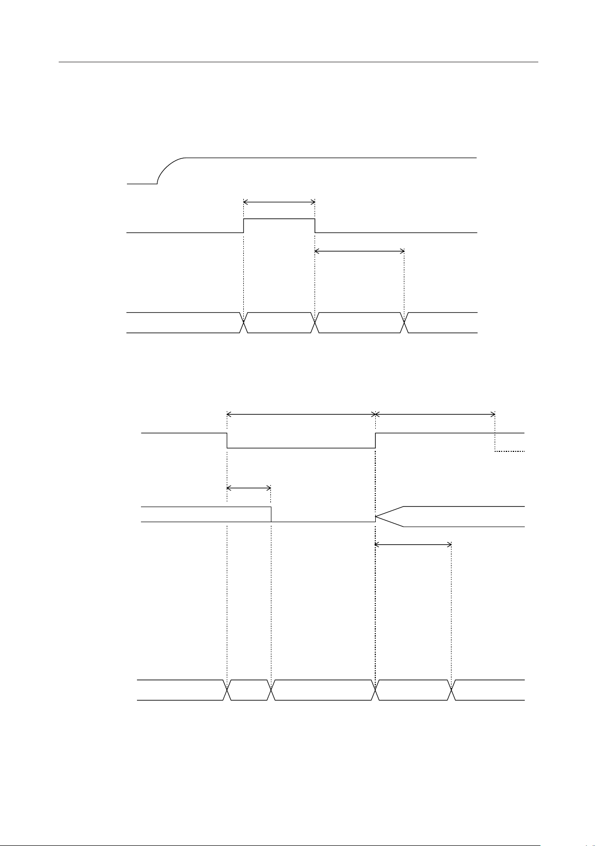
TIMING DIAGRAMS
RESET FUNCTION
V
DD
RESET (I)
t
RST
t
REX
Undefined Power down
Power Down by PDWN Pin
PDWN (I)
XT (I)
XT (O)
Oscillation in progress
tPX Note 1
t
Reset operation in progress
PDL
Standby for record/playback
t
PDH
Oscillation in progress
t
BPD
Power down Postprocessing Standby
Note: 1. When an external clock is used, continue to apply the clock input to the XT terminal
during tPX after the PDWN pin is set to a low level.
15/159
¡ Semiconductor MSM6688/6688L
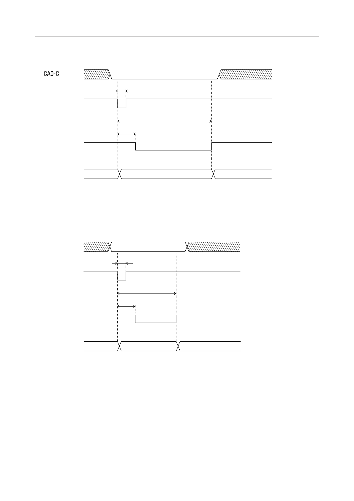
Timing for Deletion of All Phrases
CA0-CA5 (I)
t
DEL
DEL (I)
t
WBLA
t
DCS
CSI (O)
Standby
Deletion of all phrases
Timing for Deletion of a Specified Phrase
CA0-CA5 (I)
t
DEL
DEL (I)
t
WBL1
t
DCS
CSI (O)
Standby
Deletion of a specified phrase
Standby
Standby
16/159
17/159
¡ Semiconductor MSM6688/6688L
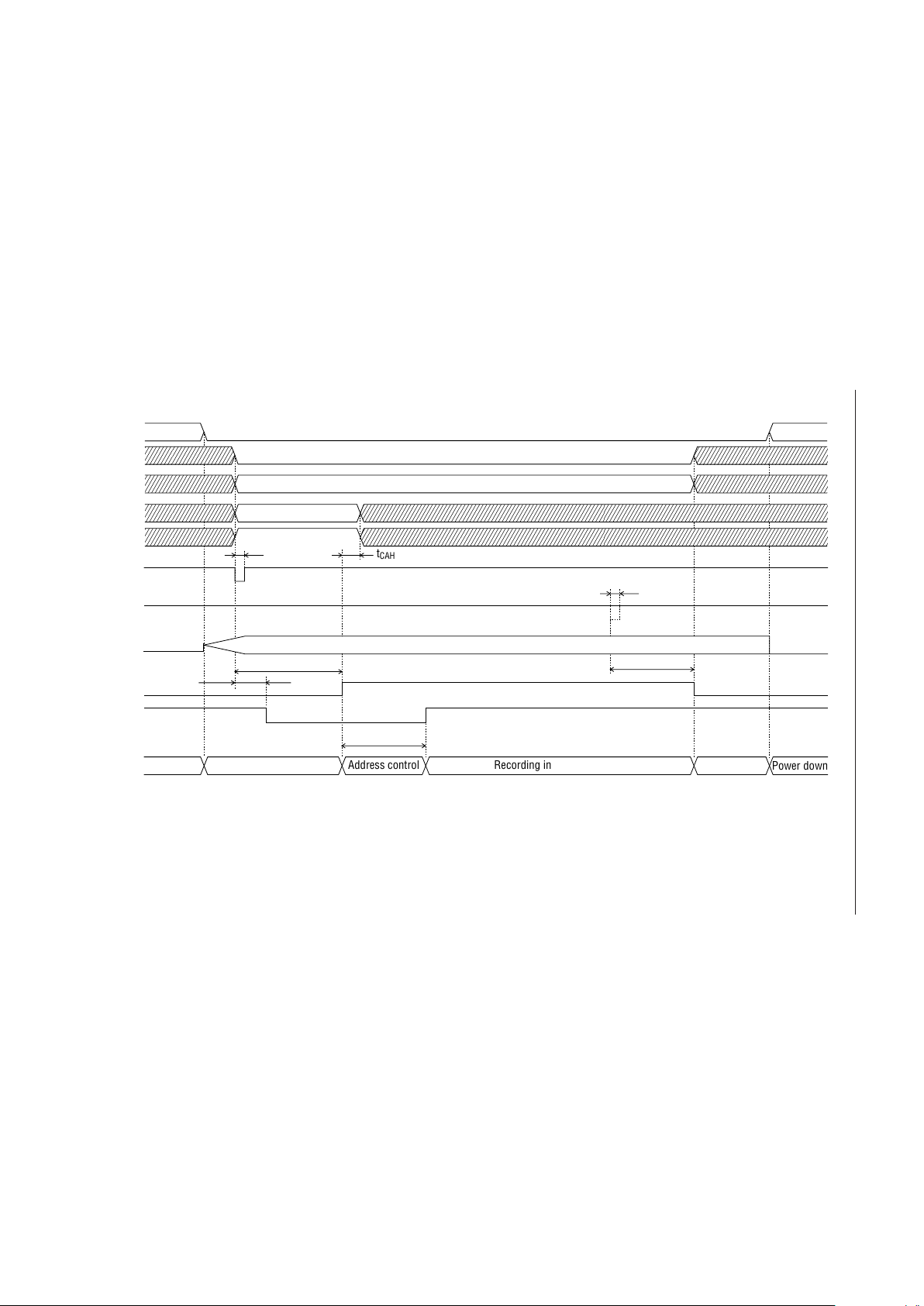
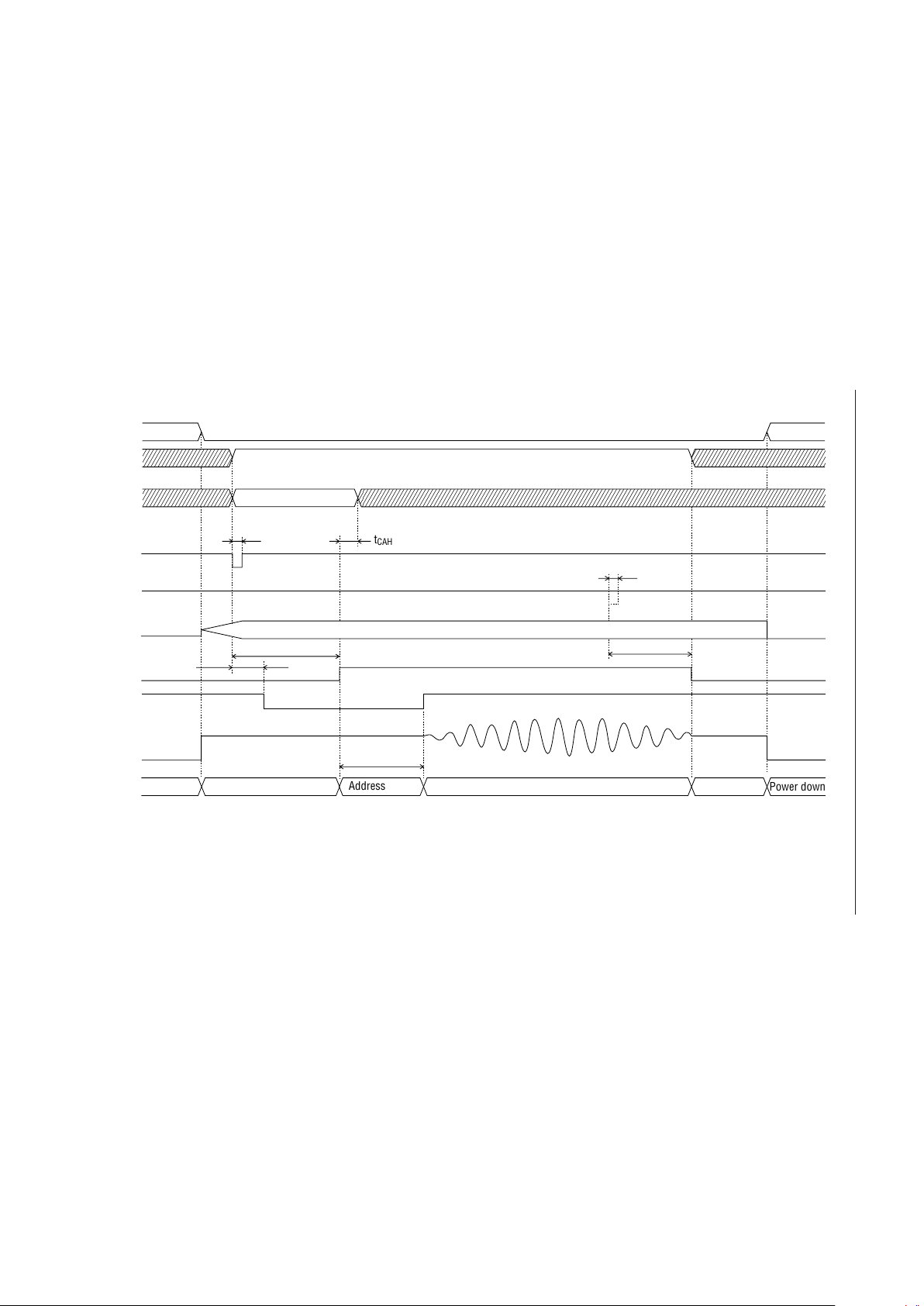
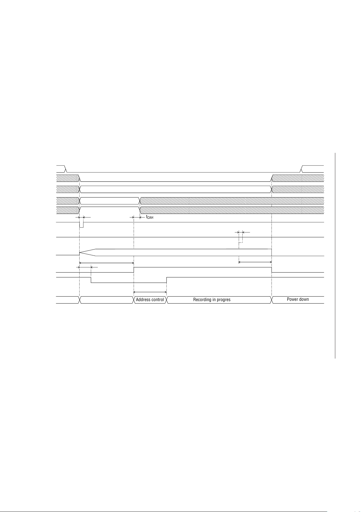
Recording Timing (PDMD Pin = High)
ST
MON
Standby
Power down
Oscillation in progress
t
TMH1
XT
t
STN
t
ST
t
CAH
Power down
Address control Recording in progress
Standby
t
SP
Phase designation
Bit rate designation
t
PMH1
t
AD1
RESET
ROM
SAM1, SAM2
4B/3B
CA0-CA5
REC/PLAY
SP
XT
NAR
(I)
(O)
(O)
(I)
(I)
(I)
(I)
(I)
(I)
(I)
(I)
(O)
18/159
¡ Semiconductor MSM6688/6688L
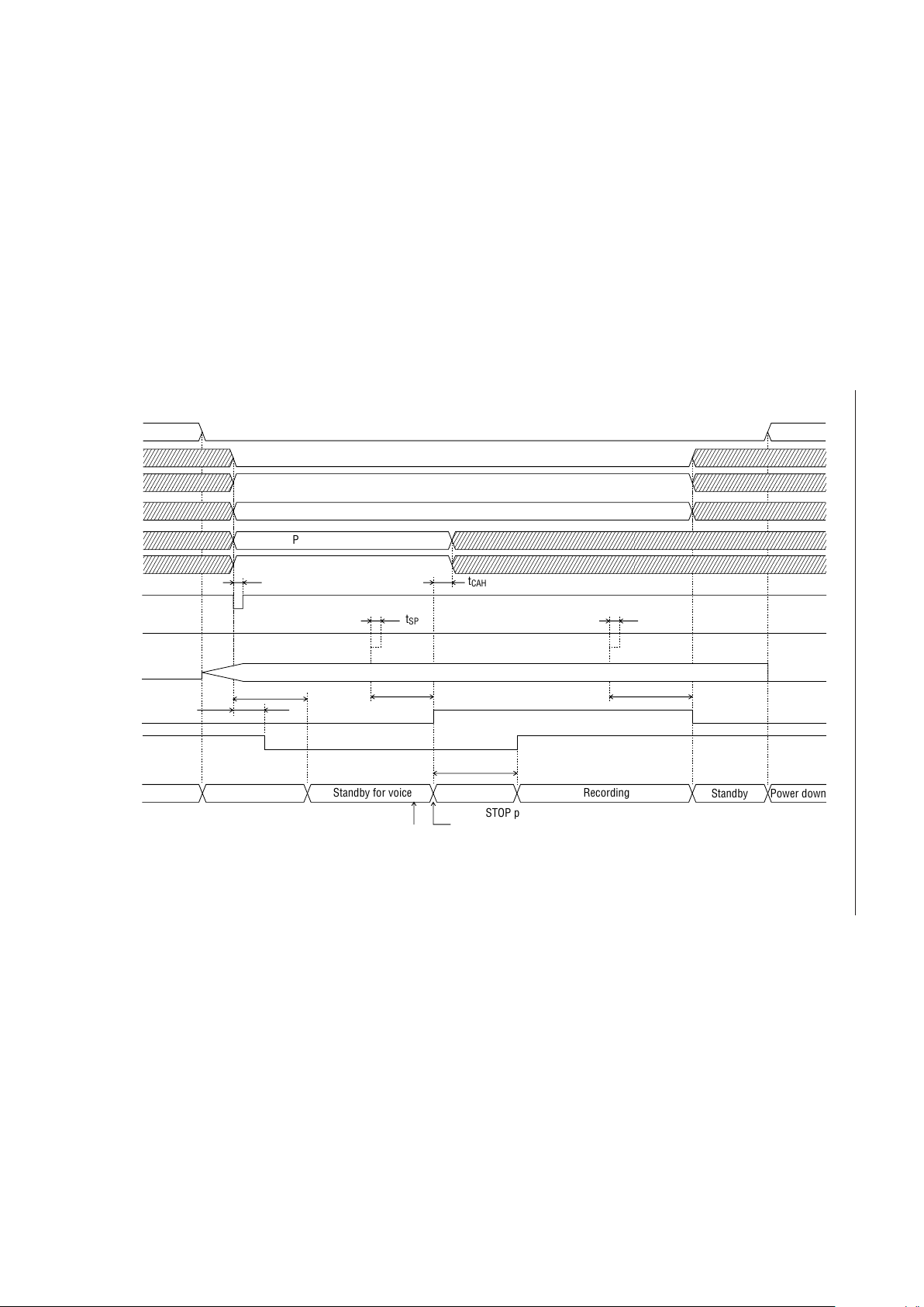
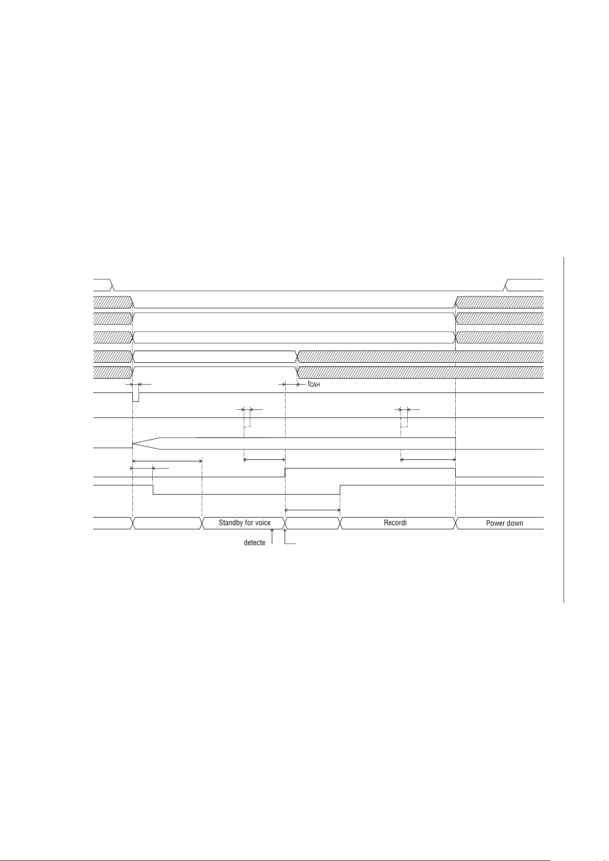
Timing for Voice Triggered Recording (PDMD Pin = High)
ST
MON
Standby
Power down
Oscillation in progress
t
STVH
XT
t
STN
t
ST
t
CAH
Power down
Standby for voice Recording
Standby
t
SP
Phrase designation
Bit rate designation
t
SPVH
t
AD1
RESET
SAM1, SAM2
4B/3B
CA0-CA5
REC/PLAY
SP
XT
NAR
(I)
(O)
(O)
(I)
(I)
(I)
(I)
(I)
(I)
(I)
(I)
(O)
ROM (I)
t
SP
t
PMH1
Address control
VDS
Voice detected
When STOP pulse is input during standby for voice,
the MSM6688 goes to the recording standby state.
19/159
¡ Semiconductor MSM6688/6688L
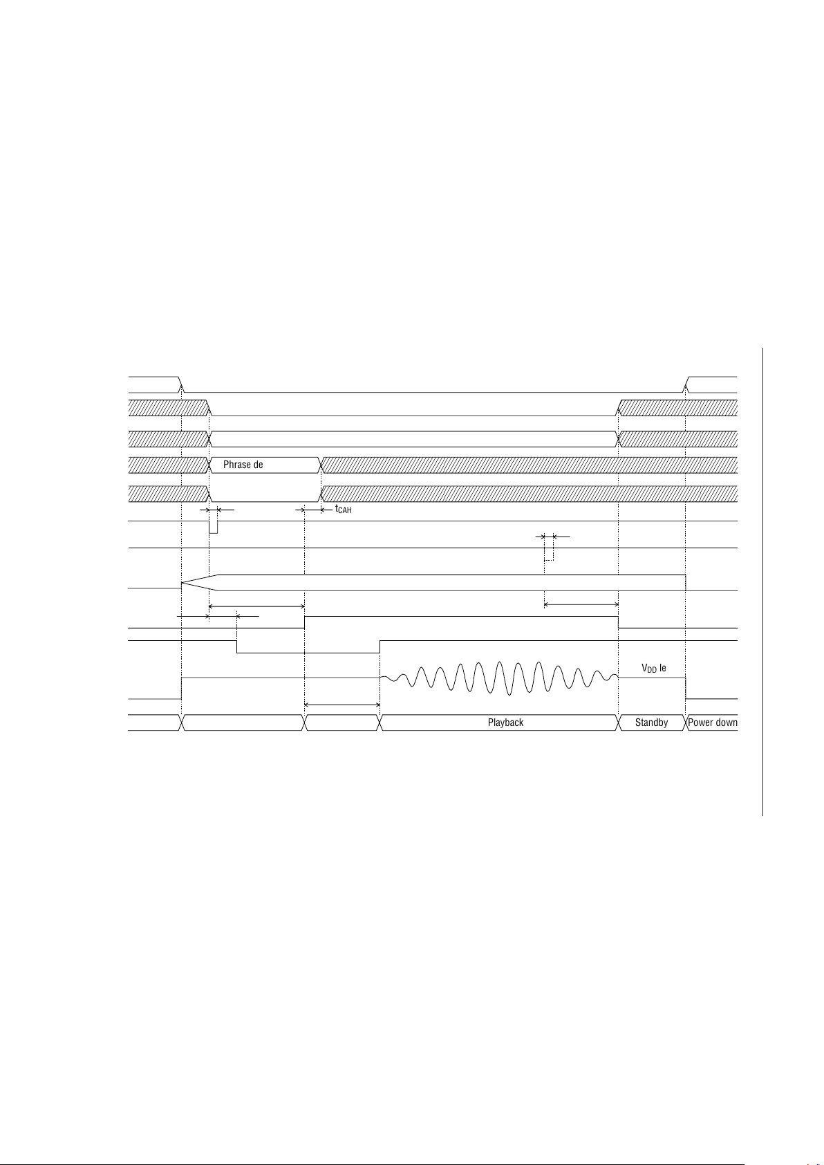
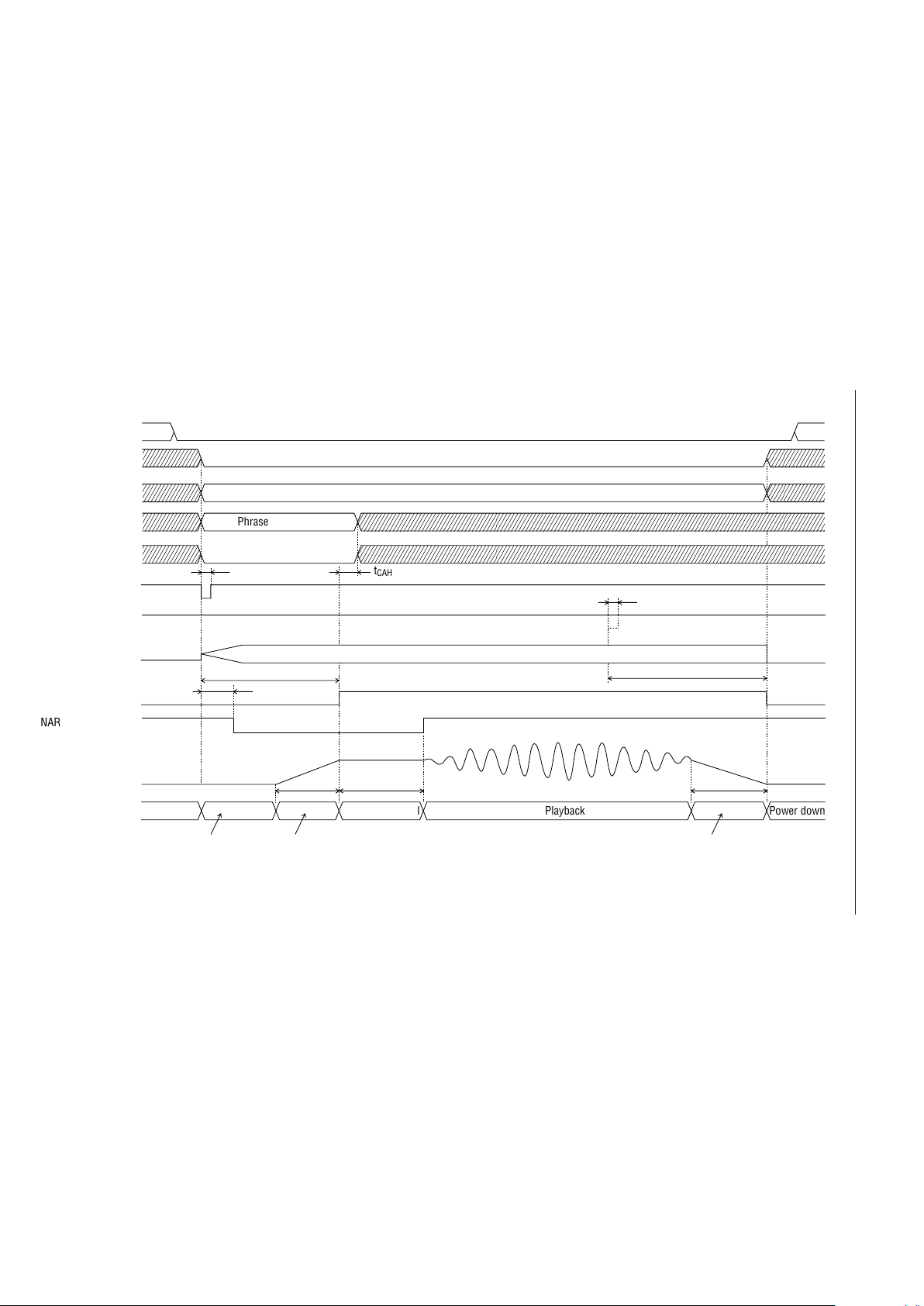
Playback Timing (PDMD Pin = High)
ST
MON
Standby
Power down
Oscillation in progress
t
TMH2
XT
t
STN
t
ST
t
CAH
Power down
Playback
Standby
Phrase designation
Bit rate designation
t
AD1
RESET
SAM1, SAM2
4B/3B
CA0-CA5
REC/PLAY
SP
XT
AOUT
(I)
(O)
(O)
(I)
(I)
(I)
(I)
(I)
(I)
(I)
(O)
RO (I)
t
SP
t
PMH2
Address control
NAR (O)
1/2 VDD level
GND level
1/2 VDD level
GND level
20/159
¡ Semiconductor MSM6688/6688L
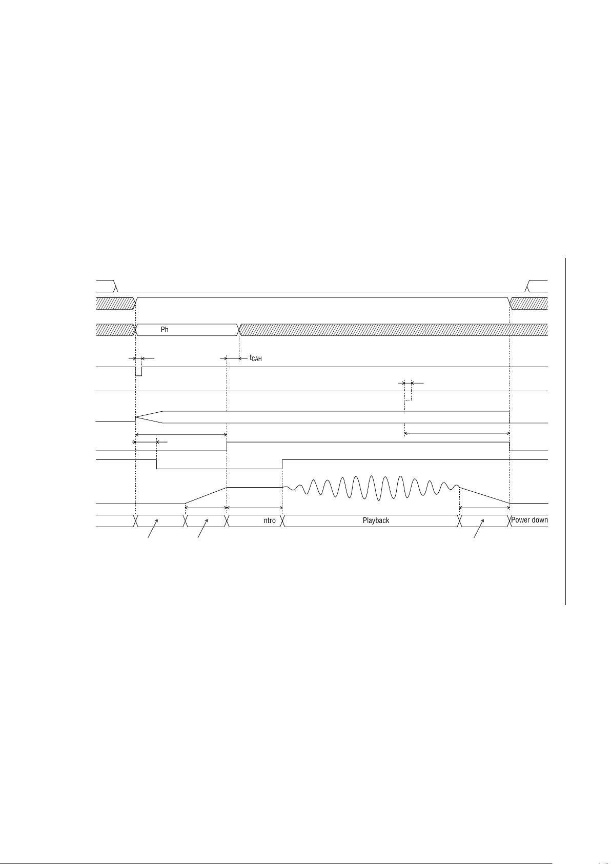
ROM Playback Timing (PDMD Pin = High)
ST
MON
Standby
Power down
Oscillation in progress
t
TMH3
XT
t
STN
t
ST
t
CAH
Power down
Playback
Standby
Phrase designation
t
AD1
RESET
CA0-CA5
SP
XT
AOUT
(I)
(O)
(O)
(I)
(I)
(I)
(I)
(O)
ROM (I)
t
SP
t
PMH3
Address control
NAR (O)
1/2 VDD level
GND level
1/2 VDD level
GND level
21/159
¡ Semiconductor MSM6688/6688L
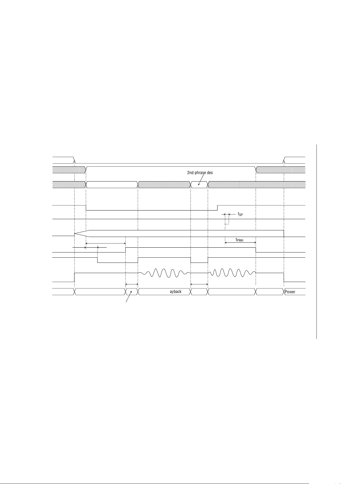
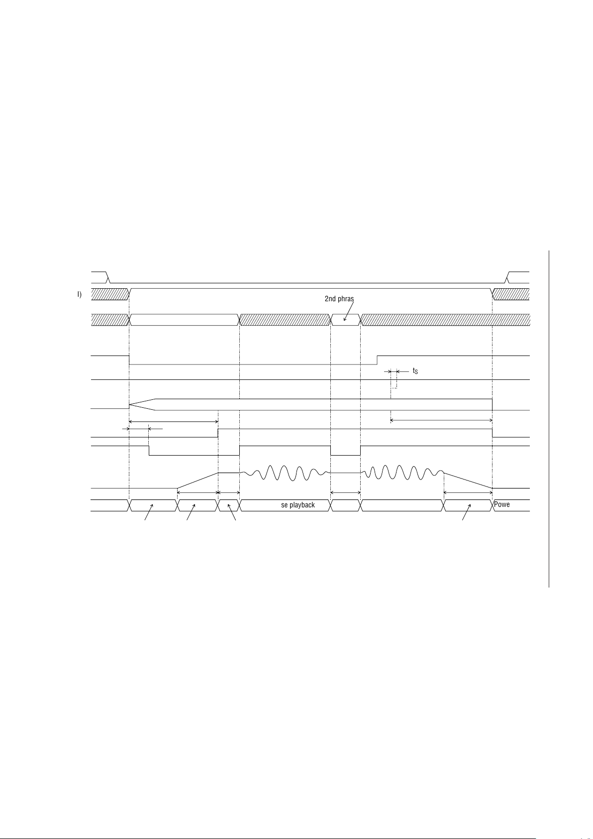
Continuous ROM Playback Timing (PDMD Pin = High)
ST
MON
Standby
Power down
Oscillation in progress
t
TMH3
XT
t
STN
Power down
Unvoiced
2nd phrase playback
1st phrase designation
t
AD1
RESET
CA0-CA5
SP
XT
AOUT
(I)
(O)
(O)
(I)
(I)
(I)
(I)
(O)
ROM (I)
t
SP
t
PMH3
Address control
NAR (O)
1/2 VDD level
GND level
1/2 VDD level
GND level
1st phrase playback
2nd phrase designation
t
MID
Standby
22/159
¡ Semiconductor MSM6688/6688L
Recording Timing (PDMD Pin = Low)
ST
MON
Analog stable time
Power down
Oscillation in progress
t
TML1
XT
t
STN
t
ST
t
CAH
Power down
Address control Recording in progress
t
SP
Phrase specifying operation
Bit rate specifying operation
t
PML1
t
AD1
RESET
ROM
SAM1, SAM2
4B/3B
CA0-CA5
REC/PLAY
SP
XT
NAR
(I)
(O)
(O)
(I)
(I)
(I)
(I)
(I)
(I)
(I)
(I)
(O)
23/159
¡ Semiconductor MSM6688/6688L
Timing for Voice Triggered Recording (PDMD Pin = Low)
ST
MON
Analog stable time
Power down
Oscillation in progress
t
STVL
XT
t
STN
t
ST
t
CAH
Power down
Standby for voice Recording
t
SP
Phrase designation
Bit rate designation
t
SPVL
t
AD1
RESET
SAM1, SAM2
4B/3B
CA0-CA5
REC/PLAY
SP
XT
NAR
(I)
(O)
(O)
(I)
(I)
(I)
(I)
(I)
(I)
(I)
(I)
(O)
ROM (I)
t
SP
t
PML1
Address control
VDS
Voice detected
When STOP pulse is input during standby for voice,
the MSM6688 goes to the recording standby state.
24/159
¡ Semiconductor MSM6688/6688L
Playback Timing (PDMD Pin = Low)
ST
MON
Analog stable time
Power down
Oscillation in progress
t
TML2
XT
t
STN
t
ST
t
CAH
Power down
Playback
Phrase designation
Bit rate designation
t
AD1
RESET
SAM1, SAM2
4B/3B
CA0-CA5
REC/PLAY
SP
XT
AOUT
(I)
(O)
(O)
(I)
(I)
(I)
(I)
(I)
(I)
(I)
(O)
ROM (I)
t
SP
t
PML2
Address control
NAR (O)
GND level
1/2 V
DD
level
GND level
Standby transition
t
AOR
t
AOF
Standby transition
25/159
¡ Semiconductor MSM6688/6688L
ROM Playback Timing (PDMD Pin = Low)
ST
MON
Analog stable time
Power down
Oscillation in progress
t
TML3
XT
t
STN
t
ST
t
CAH
Power down
Playback
Phrase designation
t
AD1
RESET
CA0-CA5
SP
XT
AOUT
(I)
(O)
(O)
(I)
(I)
(I)
(I)
(O)
ROM (I)
t
SP
t
PML3
Address control
NAR (O)
GND level
1/2 V
DD
level
GND level
Standby transition
t
AOR
Standby transition
t
AOF
26/159
¡ Semiconductor MSM6688/6688L
Continuous ROM Playback Timing (PDMD Pin = Low)
ST
MON
Power down
Oscillation in progress
t
TML3
XT
t
STN
Power down
Unvoiced
2nd phrase playback
1st phrase designation
t
AD1
RESET
CA0-CA5
SP
XT
AOUT
(I)
(O)
(O)
(I)
(I)
(I)
(I)
(O)
ROM (I)
t
SP
t
PML3
Address control
NAR (O)
GND level
1/2 V
DD
level
GND level
1st phrase playback
2nd phrase designation
t
MID
Standby transitionAnalog stable time
t
AOR
t
AOF
Standby transition
27/159
¡ Semiconductor MSM6688/6688L
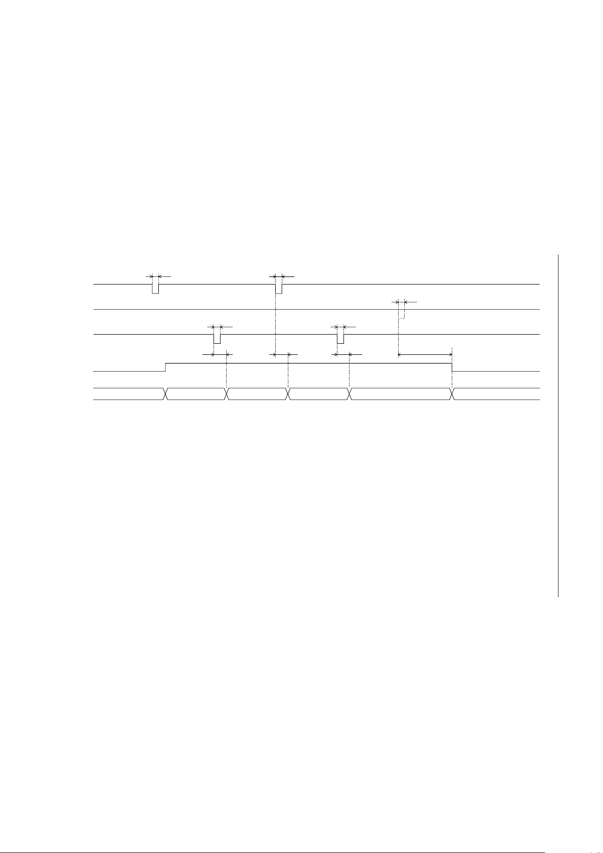
Record/Playback Pause Timing
ST
MON
Standby
Pause
SP
(I)
(O)
(I)
t
ST
Note 1
t
PST
Record/PlaybackPauseRecord/PlaybackStandby
t
ST
t
PSE
t
SP
t
PSE
t
PP
t
PP
PAUSE
(I)
Start pulse Restart pulse
Note 1: This time interval varies depending on the state of PDMD pin and
the record/playback mode and is one of t
PMH1
, t
PMH2
, t
PMH3
, t
PML1
,
t
PML2
and t
PML3
.
¡ Semiconductor MSM6688/6688L
FUNCTIONAL DESCRIPTION
Recording Time and Memory Capacity
The recording time depends on the memory capacity of the external serial registers, sampling
frequency, and ADPCM bit length, and is given by
Recording time = (seconds)
1.024 ¥ memory capacity (K bits)
sampling frequency (kHz) ¥ bit length (bits)
For example, if the sampling frequency is kHz (= 5.333 kHz), ADPCM bit length is 3 bits, and
4096
768
four 8M bit serial registers are used, the recording time can be obtained as follows.
Recording time = = 2093 seconds
1.024 ¥ (8192 ¥ 4 – 64)
5.333 ¥ 3
= 34 minutes 53 seconds
In the above equation, the memory capacity is obtained by subtracting the memory capacity (64
Kbits) for the channel index area from the total memory capacity.
Connection of an Oscillator
Connect a ceramic oscillator or a crystal oscillator to XT and XT pins as shown below. The optimal
load capacities when connecting ceramic oscillators from MURATA MFG. and KYOCERA
CORPORATION are shown below for reference.
MSM6688
XTXT
MURATA
MFG.
KYOCERA
CORPORATION
CSA4.00MG
CST4.00MGW
CSA6.00MG
CST6.00MGW
CSA8.00MTZ
CST8.00MTW
KBR-4.0MSA
KBR-4.0MKS
PBRC4.00A
PBRC4.00B
KBR-6.0MSA
KBR-6.0MKS
PBRC6.00A
PBRC6.00B
KBR-8.0M
PBRC8.00A
PBRC8.00B
C
1
Ceramic oscillator Optimal load capacity
Type Freq(MHz) C
(with capacitor)
(with capacitor)
(with capacitor)
(with capacitor)
(with capacitor)
2
C
1
(pF) C2(pF)
4.0
6.0
8.0
4.0
6.0
8.0
30
33 33
30
28/159
¡ Semiconductor MSM6688/6688L
Power Supply Wiring
As shown in the following diagram, supply the power to this MSM6688 from the same power source,
but separate the power supply wiring to the analog portion from that to the logic position.
+5V
DV
DV
DD
DD'
DGND AGND
MSM6688
AV
DD
The following connections are not permitted.
Analog power supply
Digital power supply
DV
DV
DD
DD'AVDD
+5V
DV
DV
DD'
DD
AV
DD
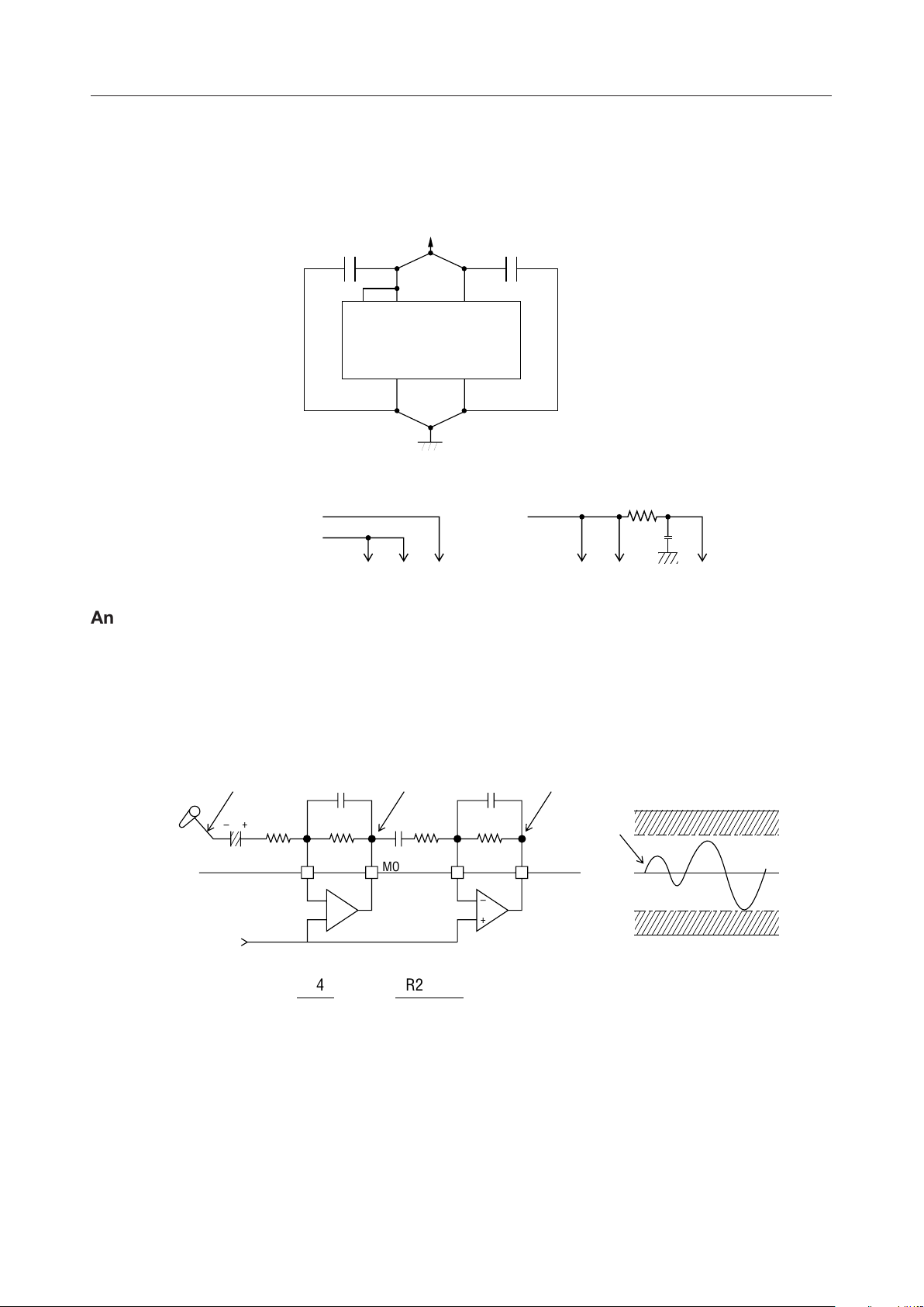
Analog Input Amplifier Circuit
This MSM6688 has two built-in operational amplifiers for amplifying the microphone output. Each
OP amplifier is provided with the inverting input pin and output pin. The analog circuit reference
voltage SG (signal ground) is connected internally to the non-inverting input of each OP amplifier.
For amplification, form an inverting amplifier circuit and adjust the amplification ratio by using
external resistors as shown below.
V
IN
+
–
R1 R3 R4
R2
V
MO
V
LO
V
DD
V
LO
VDD–1
SG
VLO=
MIN
–
+
R4 R2 • R4
R3 R1 • R3
MOUT LIN LOUT
–
OP amp 1 OP amp 2
=V
V
MO
+
(V)
IN
1/2V
1
GND
DD
During the time the recording operation is performed, the output VLO of OP amp 2 is connected to
the input FIN of the built-in LPF. The FIN allowable input voltage (V
) ranges from 1V to (V
FIN
DD
– 1)V. Therefore, the amplification ratio must be adjusted so that the VLO amplitude can be within
the FIN allowable input voltage range.
For example, if VDD = 5V, V
becomes 3 V
LO
max. If VLO exceeds the FIN allowable input voltage
p-p
range, the output of the LPF will be a clipped waveform.
The load resistance R
of the OP amp is 200 kW minimum, so that the feedback resistors R2 and
OUTA
R4 of the inverting amplifier circuit must be 200 kW or more.
29/159
¡ Semiconductor MSM6688/6688L
Connection of LPF Circuit Peripherals
The AMON pin is connected internally to the output of the amplifier circuit (LOUT pin) in the
recording mode and to the output of the built-in DA converter in the playback mode. Therefore,
connect the AMON pin directly to the input (FIN pin) of the built-in LPF.
Both the FOUT and AOUT pins are the output pins of the built-in LPF. Connect the FOUT pin to the
input (ADIN pin) of the built-in AD converter and connect the AOUT pin to an external speaker
through an external speaker drive amplifier.
In the MSM6688, the connection of each of the FOUT and AOUT pins is changed to one of the output
of the LPF, GND (ground) level, and SG (signal ground) level, depending on the operation status as
shown below.
When PDMD pin = high level:
During operation
Analog pin
At power down
(RESET pin = H)
Recording mode Playback mode
(RESET pin = L)
FOUT pin
AOUT pin
When PDMD pin = L:
Analog pin At power down
FOUT pin
AOUT pin
GND level
GND level
GND level
GND level
LPF output
(recording waveform)
SG level
During operation
Recording mode Playback mode
LPF output
(recording waveform)
GND level
LPF output
LPF output
(playback waveform)
LPF output
LPF output
(playback waveform)
30/159

¡ Semiconductor MSM6688/6688L
(
)
When PDMD pin = H:
Speaker drive amplifier
When PDMD = L:
LOUT AMON
Record mode
–
+
SG
DAC
SG
Playback mode
Note: This diagram shows the state of each switch during the recording operation.
LOUT AMON
–
+
Record mode
Playback mode
FIN
FIN
LPF
LPF
Playback
mode
Record mode
SG
–
+
–
+
–
+
GND
GND
AOUTLIN
Power down
Speaker drive amplifier
AOUTLIN
Playback
FOUT ADIN
Power down
FOUT ADIN
ADC
ADC
DAC
Note: This diagram shows the state of each switch during the recording operation.
LPF Characteristics
This IC contains a fourth-order switched-capacitor
LPF.
The attenuation characteristic of this LPF is –40 dB/
oct. The cut-off frequency and frequency
characteristics of this LPF vary in proportion to the
sampling frequency (fsamp). The cut-off frequency
is preset to 0.4 times the sampling frequency. The
following graph depicts the frequency characteristics
of the LPF at fsamp = 8␣ kHz.
[dB]
–
+
Power down
GND
20
10
0
–10
–20
–30
–40
–50
–60
–70
–80
100 1K 10K [Hz]
LPF Frequency Characteristics
fsamp = 8.0 kHz
31/159

¡ Semiconductor MSM6688/6688L
Reset Function
By applying a high level to the RESET pin, the MSM6688 stops frequency oscillation to minimize
current consumption and goes to the power-down state. At the same time, the control circuit is reset
and initialized.
If a high level is applied to the RESET pin during record/playback operation , the MSM6688 is set
to the power-down state and initialized state, so that voice data becomes undefined.
The following shows the power-down state of the MSM6688.
(1) Frequency oscillation is stopped and all operations of the internal circuit are halted.
(2) The current consumption is minimized. When an external clock is used, apply a ground (GND)
level to the XT pin at power down so that no current can flow into the oscillation circuit.
(3) CS1 – CS4 pins are set to a high level to minimize the current consumption of external serial
registers and serial voice ROMs.
(4) Pull-up resistors are removed from the input control ST, SP, PAUSE, and DEL pins.
(5) The state of the output pins are as follows.
Pin name
SAS, TAS, CS1-CS4, RWCK "H" level "H" level
SADX, WE, NAR "H" level "H" level or "L" level
SADY "L" level "H" level or "L" level
MON "L" level "L" level
AOUT, FOUT GND level GND level
Power down mode
with RESET="H"
Power down mode
with PDWN="L"
After powering up the MSM6688, be sure to initialize it by applying a high level to the RESET pin.
32/159

¡ Semiconductor MSM6688/6688L
Power Down by the PDWN pin
By applying a low level to the PDWN pin, the MSM6688 may be set to the power-down state, in which
the oscillation and all operations of internal circuits are halted. Unlike the reset operation by the
RESET input, the control circuit will not be initialized by this power-down operation.
The power-down operation will not affect the data in the internal control circuit and external serial
registers. Therefore, this power-down operation is useful when the battery backup takes place in
case of power failure.
When PDWN becomes low during one of the following operations, their respective operations will
be performed after the power-down state is released (PDWN = H).
(1) When the MSM6688 is powered down (PDWN = L) during the record/plaback operation: The
record/playback operation is stopped. After the release of the power-down state, the
postprocessing will be performed.
(2) When the MSM6688 is powered down (PDWN = L) during the phrase deleting operation: The
phrase deleting operation is temporarily stopped and will be restarted after the release of the
power-down state.
(3) When the MSM6688 is powered down (PDWN = L) during the time the transition of the AOUT
output to a DC level is in progress: This transition operation is temporalily stopped and
will be continued after the release of the power-down state.
33/159

¡ Semiconductor MSM6688/6688L
Record/Playback Control Mode
Either record/playback mode or ROM playback mode can be selected through the ROM pin as
described below.
ROM pin Record/playback control mode
L Record/playback
H ROM playback
1. Record/playback
The recorded voice data is stored in serial registers. The recording area is indirectly allocated to each
phrase by setting the phase specifying pins CA0 to CA5 (63 phrases). The recording area for each
phrase is managed by the MSM6688 as described below.
The total memory capacity of the connected external serial registers is equally divided into 256
memory blocks. When recording is performed, voice data is written into the memory blocks unused
by other phrases. When a specified phase is deleted, the blocks used by this phrase become unused
blocks.
When re-recording is performed, voice data is written in the memory area consisting of the memory
blocks used by this phrase and the unused memory blocks.
The memory capacity of one memory block and the number of initially available memory blocks
(recording time) vary according to the total memory capacity of the connected serial registers.
RSEL2 L L H H
RSEL1 L H L H
Total memory capacity 8M bits 16M bits 24M bits 32M bits
Memory capacity of one block 32K bits 64K bits 128K bits 128K bits
16kbps
Recording time
of one block
Number of initially available
blocks
24kbps
32kbps
2.0 seconds 4.1 seconds 8.2 seconds 8.2 seconds
1.4 seconds 2.7 seconds 5.5 seconds 5.5 seconds
1.0 second 2.0 seconds 4.1 seconds 4.1 seconds
254 255 191 255
34/159

¡ Semiconductor MSM6688/6688L
2. ROM playback
For playback of the voice data stored in the connected serial voice ROM, the playback area is
allocated indirectly to each fixed message phrase by setting phrase specifying pins CA0 to CA5 (63 phases).
The start address, stop address, sampling frequency, and ADPCM bit length which specify the
playback area for each phase are written in the index area of the serial voice ROM. When the playback
operation is started, the MSM6688 fetches these data from the index area.
35/159

¡ Semiconductor MSM6688/6688L
Deleting phrases
1. Deleting all phrases
All 63 phrases ch01 through ch3F can be deleted by specifying ch00 and applying a low pulse to the
DEL pin. When all phrases are deleted, all phrases ch01– ch3F (63 phrases) go to the unrecorded
status and, at the same time, the initial data for address control is written in the serial registers.
Therefore, whenever the MSM6688 is powered up, delete all phrases after applying a high level to
the RESET pin.
2. Deleting a specified phrase
By specifying one of ch01 - ch3F phrase and applying a low level to the DEL pin, the specified phrase
can be deleted and put to the unrecorded state. The blocks for the deleted phrases are added to
available unused blocks (available recording time).
36/159

¡ Semiconductor MSM6688/6688L
Recording Method
Whenever the MSM6688 is powered up, be sure to delete all phrases after applying a high level to
the RESET pin. Then, start the recording operation.
(1) Set recording conditions at the relevant pins.
ROM pin: Low level
REC/PLAY pin: High level
VOS pin: Selection of voice triggered starting (high level enables voice activation
and low level disables voice activation.)
SAM1 and SAM2 pins: Select the sampling frequency.
4B /3B pin: Select the ADPCM bit length.
CA0 – CA5 pins: Specify one of 63 phrases ch01 – ch3F.
(2) To start recording, apply a low pulse to the ST pin.
To stop recording in progress, apply a low pulse to the SP pin. When recording continues to the
end of the memory capacity, recording is automatically stopped. In case of re-recording, voice
data will be written in the memory block used by the specified phrase and unused memory
blocks. Therefore, the voice data is overwritten on the previously recorded contents. The MON
pin outputs a high level during recording.
ST
SP
MON
ST
MON
(I)
(I)
(O)
(I)
(O)
Start pulse Invalid
Stop pulse
Recording in progress
(stopped in the middle)
Available memory capacity
Start pulse
Recording in progress
Available memory capacity
Recording is stopped automatically.
37/159

¡ Semiconductor MSM6688/6688L
Playback Method
(1) Set playback conditions at the relevant pins.
ROM pin: Low level
REC/PLAY pin: Low level
SAM1 and SAM2 pins: Select the sampling frequency.
4B/3B pin: Specify the ADPCM bit length selected for recording.
CA0–CA5 pins: Specify one of 63 phases ch01–ch3F.
(2) To start playback, apply a low pulse to the ST pin.
When playback for the duration of the recorded data is finished, the playback is stopped
automatically.
To stop playback in progress, apply a low pulse to the SP pin.
The MON pin outputs a high level during playback.
Start pulse
ST
(I)
MON
(O)
Playback in progress (same as the recorded time)
Playback is stopped automatically
Start pulse
(I)
ST
SP
MON
(I)
(O)
Playback in progress
(stopped in the middle)
Recorded time
Stop pulse
By maintaining the ST pin at a low level, repeated playback is possible.
ST
SP
MON
(I)
(I)
(O)
(Stop pulse)
2nd playback1st playback
3rd playback
38/159

¡ Semiconductor MSM6688/6688L
ROM Playback Method
(1) Apply a high level to the ROM pin.
(2) Specify one of 63 phrases ch01 – ch3F by setting the CA0 – CA5 pins.
(3) To start playback, apply a low pulse to the ST pin. To stop playback in progress, apply a low
pulse to the SP pin.
39/159

¡ Semiconductor MSM6688/6688L
Voice Triggered Starting
This MSM6688 has the voice triggered starting function that starts recording when the level of voice
input exceeds a preset amplitude. Using the voice activated function, the unvoiced part prior to voice
detection will not be recorded, so that the memory capacity can be utilized efficiently.
The unvoiced parts in the middle of recording are not eliminated. In the voice triggered starting
mode, recording is started when a voice input exceeds the preset thresholds. Therefore, a consonant
part with a low level may not be recorded.
Voice input level
(ADIN pin)
1/2V
DD
Start signal input
VDS pin Voice triggered starting conditions
L
H
Voice triggered starting disabled
Voice triggered starting enabled
Voice detection threshold Vvds = V
/32 (±160 mV)
DD
Upper threshold
+Vvds
–Vvds
Lower threshold
Identified as voice
The value in parentheses is for VDD = 5.12V.
40/159

¡ Semiconductor MSM6688/6688L
When a low level is applied to the ST pin, the MSM6688 goes to the standby state for voice. When
detecting a voiced input, it starts recording and the MON pin outputs a high level.
Start pulse
(I)
ST
SP
MON
(I)
(O)
Stop pulse
Standby for voice
Determined as voice
Recording in progress
When a low level is applied to the SP pin during standby state for voice, the MSM6688 finishes the
standby state for voice and goes to the standby state for recording.
Start pulse
(I)
Stop pulse
SPST(I)
Standby for
recording
Standby for voice
Standby for
recording
41/159

¡ Semiconductor MSM6688/6688L
Method of Temporarily Stopping Record/Playback by Pause Function
By applying a low pulse to the PAUSE pin during record/playback, record/playback operation can
be stopped temporarily. To resume record/playback, apply a low pulse to the ST pin. To stop
record/playback, apply a low pulse to the SP pin.
Start pulse
Resume
Stop pulse
PAUSEST(I)
ST (I)
SP (I)
PAUSE (I)
Start pulse
(I)
Start pulse
Pause pulse
Pause
Pause pulse
Pause
Record/Playback finished
When record/playback is resumed after temporary stop, the voice triggered starting circuit is not
operated and recording is started when a start low pulse is applied to SP pin.
42/159

¡ Semiconductor MSM6688/6688L
APPLICATION CIRCUIT
The circuit diagram 1 shows an application circuit example where the MSM6688 is used in the standalone mode and four 8M bit serial registers and two 2M bit serial voice ROMs also connected.
MSM6596A-XXX
2M SERIAL VOICE ROM
SAS
SASX
SADY
SADY
MSM6596A-XXX
TAS
RDCK
SASY
TAS
RWCK
V
CC
SADX
SADX
MSM6685
MSM6685
MSM6685
8M SERIAL REGISTER MSM6685
CC
V
SAD
SAS
TAS
RWCKWEWE
DIN
DROM
DOUT
TEST
DOUT
NC
TEST
V
CS1 CS2
TEST
CS V
TEST
SS
mode with 8M bit serial registers
and 2M bit serial voice ROMs
Circuit Diagram 1: Application circuit in standalone
SS
AV
'DV
DV
SADX
SAS
TAS
RWCK
DI/O
Speaker drive amplifier
+
+
DD
DD
DD
REC/PLAY
DEL
SADX
SAS
ST
SADY
SP
TAS
RWCK
PAUSE
WE
RESET
PDWN
DI/O
DROM
CS1
CS4
CS3
CS2
ADPCM SOLID-STATE RECORDER IC MSM6688
RSEL1
RSEL2
SAM1
SAM2
4B/3B
PDMD
MCUM
VDS
CA0
CA1
CA2
CA3
SW
Phrase
selector
CA4
MIN
CA5
MOUT
ROM
LIN
XT
XT
LOUT
FIN
AMON
ADIN
FOUT
MON
NAR
4.096 MHz
AOUT
SGC
SG
AGND
DGND
43/159

¡ Semiconductor MSM6688/6688L
(2) MICROCONTROLLER INTERFACE MODE (for MSM6688 (5 V Version)
and MSM6688L (3 V Version))
FEATURES
• 3-bit or 4-bit ADPCM
• Built-in 12-bit AD converter
• Built-in12-bit DA converter
• Built-in microphone amplifier
• Built-in low-pass filter
Attenuation characteristics –40 dB/oct
• External only registers (for variable messages)
MSM6688 (5 V version)
- Serial registers, 32M bits maximum
One 4M bit serial register (MSM6684B) can be driven directly
Up to four 8M bit serial register (MSM6685) can be driven directly
MSM6688L (3 V version)
- Serial registers, 4M bits maximum
One 4M bit serial register (MSM66V84B) can be driven directly
• External only ROMs (for fixed messages)
- Serial voice ROMs, 4M bits maximum
1M bit serial voice ROM (MSM6595A) can be driven directly
2M bit serial voice ROM (MSM6596A) can be driven directly
3M bit serial voice ROM (MSM6597A) can be driven directly
• Sampling frequency
4.0 kHz, 5.3 kHz, 6.4 kHz or 8.0 kHz (master clock frequency = 4.096 MHz)
8.0 kHz, 10.6 kHz, 12.8 kHz or 16.0 kHz (master clock frequency = 8.192 MHz)
• Number of phrases
63 phrases for variable messages
63 phrases for fixed messages
• Maximum recording time (when external 32M bit RAM is connected)
34 minutes (for 16 kbps ADPCM)
23 minutes (for 24 kbps ADPCM)
17 minutes (for 32 kbps ADPCM)
• Voice triggered starting function
• Pause function
• Master clock frequency: 4.096 MHz to 8.192 MHz
• Power supply voltage
MSM6688: Single 5 Vpower supply
MSM6688L: Single 3 V power supply
• Package options:
56-pin plastic QFP (QFP56-P-910-0.65-2K) (Product name: MSM6688GS-2K)
56-pin plastic QFP (QFP56-P-910-0.65-2K) (Product name: MSM6688LGS-2K)
64-pin plastic TQFP (TQFP64-P-1010-0.50-K) (Product name: MSM6688LTS-K)
44/159

45/159
¡ Semiconductor MSM6688/6688L
TEST
TEST
MCUM
RESET
PDWN
ACON
MON
NAR VPM RPM
BUSY
CE
XT
XT
MIN
MOUT
LIN
OSC
–
+
–
+
LOUT AMON FIN AOUT FOUT ADIN SG SGC
SADX
SADY
TAS
RWCK
WE
CS1
CS2
CS3
CS4
RSEL1
RSEL2
DI/O
DROM
Data
I/O
Register
Controller
ADPCM
Analyzer/Synthesizer
LPF
12bit
ADC
12bit
DAC
SG
Circuit
DV
DD
DV
DD'
AV
DD
DGND
AGND
Address Controller
Test
Circuit
MCU I/F
Status
Register
CERDWRD0D1D2D3
Timing
Controller
BLOCK DIAGRAM

¡ Semiconductor MSM6688/6688L
PIN CONFIGURATION (TOP VIEW)
D0
D1
D2
D3
BUSY
RPM
VPM
ACON
TEST
MCUM
CE
TEST
TEST
TEST
CERDWR
56
1
2
3
4
5
6
7
8
9
10
11
12
13
14
15161718192021222324252627
TEST
RESET
NAR
MON
RWCK
DVDDXTXTWE
55545352515049484746454443
DD
DD'
ADIN
FOUT
AOUT
FIN
AMON
DV
AV
SG
SGC
DROM
LIN
LOUT
DI/0
MOUT
CS4
28
MIN
42
41
40
39
38
37
36
35
34
33
32
31
30
29
CS3
CS2
CS1
SADX
SADY
TAS
SAS
PDWN
TEST
TEST
RSEL2
RSEL1
DGND
AGND
56-Pin Plastic QFP
D0
D1
D2
D3
NC
BUSY
RPM
VPM
ACON
TEST
MCUM
NC
CE
TEST
TEST
TEST
CERDWR
64
1
2
3
4
5
6
7
8
9
10
11
12
15
16
17181920212223242526272829
TEST
RESET
NAR
MONNCRWCK
6362616059585756555453
NC
NC
ADIN
FOUT
AOUT
FIN
AMON
DVDDXTXTNC
DD
SG
SGC
AV
WE
52
LIN
LOUT
50 DI/031MIN
51 DROM30MOUT
CS4
49
32
NC
48
47
46
45
44
43
42
41
40
39
38
37
3613
3514
34
33
CS3
NC
CS2
CS1
SADX
SADY
TAS
SAS
PDWN
NC
TEST
TEST
RSEL2
RSEL1
DGND
AGND
NC: No connection
64-Pin Plastic TQFP
46/159

¡ Semiconductor MSM6688/6688L
PIN DESCRIPTIONS
QFP
49
21
22
30
29
23
24
28
26
27
25
20
19
Pin
TQFP
56
—
25
34
33
26
27
31
29
30
28
24
23
Symbol Type Description
DV
DV
AV
DD
DD'
DD
—
— Digital power supply pin
—
Digital power supply pin. Insert a bypass capacitor of 0.1µF or more
between this pin and the DGND pin.
Analog power supply pin. Insert a bypass capacitor of 0.1µF or more
between this pin and the AGND pin.
DGND — Digital ground pin
AGND — Analog ground pin
SG
SGC
MIN
LIN
MOUT
LOUT
O Output pin for analog circuit reference voltage (signal ground)
I
O
Inverting input pin of the built-in OP amplifier. Non-inverting input pin
is internally connected to SG (signal ground).
MOUT and LOUT are output pins of the built-in OP amplifier for MIN
and LIN, respectively.
This pin is connected to the LOUT pin in the recording mode and to the
AMON O
DA converter output in the playback mode. Used to connect the built-in
LPF input (FIN pin).
FIN I Input pin of the built-in LPF.
17
16
18
39
38
36
37
50
46
21
19
22
44
43
41
42
57
52
FOUT O
Output pin of the built-in LPF. Used to connect the AD converter input
(ADIN pin)
ADIN I Input pin of the built-in 12-bit AD converter.
AOUT O
Output pin of the built-in LPF. This pin outputs playback waveforms
and used to connect an external speaker drive amplifier.
(Serial Address Data). SADX is used to connect the SAD pin of each
SADX
SADY
O
external serial register and the SADX pin of each external serial voice
ROM. SADY is used to connect the SADY pin of each external serial
voice ROM. Outputs of starting address of read/write.
(Serial Address Strobe). Used to connect the SAS pin of external
SAS O
serial register and the SASX and SASY pins of external serial voice ROM
Clock pin to write the serial address.
(Transfer Address Strobe). Used to connect the TAS pin of each
external serial register and serial voice ROM.
TAS O
This pin outputs address strobe outputs to set the serial address data
from the SADX and SADY pins into the internal address counter of each
serial register and serial voice ROM.
(Read/Write Clock). Used to connect the RWCK pin of each external
RWCK O
serial register and the RDCK pin of each external serial voice ROM.
This pin outputs a clock to read data from or write it into each external
serial register.
WE O
(Write Enable) Used to connect the WE pin of each external serial
register. This pin outputs WE signal to select either read or write mode.
44
45
50
51
DI/O I/O
DROM I
(Data I/O). Used to connect the DIN and DOUT pins of DRAM and
serial register. This pin outputs the data to be written into the serial
register or inputs the data read from the serial registers.
(Data ROM). Used to connect the DOUT pin of each external serial
voiceROM.
47/159

¡ Semiconductor MSM6688/6688L
QFP
40
41
42
43
31
32
10
53
35
Pin
TQFP
45
46
48
49
35
36
11
61
40
Symbol Type Description
CS1
CS2
CS3
CS4
RSEL1
RSEL2
MCUM I
RESET I
PDWN I
O
I
(Chip Select). Used to connect the CS pin of serial register and the
CS (CS1, CS2, CS3) pins of each serial voice ROM.
(Register Select). These are used to select the number of external
serial registers.
RSEL2
RSEL1
Number of serial registers
This pin is used to select either the stand-alone mode or the
microcontroller interface mode.
Low level: Stand-alone mode
High level: Microcontroller interface mode
A high input level at this pin causes the MSM6688/6688L to be
initialized and to go into the power down state.
(Power Down). When a low level is input to this pin, the MSM6688
goes to the power down state. Unlike the RESET pin, this pin does
not force to reset the MSM6688/6688L. When an low level is applied
to this PDWN pin during recording operation, the MSM6688/6688L is
halted, and will be maintained in the power down state while PDWN is
low. After this pin is restored to a high level, postprocessing for
recording will be performed.
LLH
LHLH
1234
H
1
2
3
4
54
55
56
11
5
6
1
2
3
4
62
63
64
13
D0
D1
D2
D3
WR I
RD I
CE
CE
6
7
BUSY O
RPM O
I/O
I
Bi-directional data bus to transfer commands and data to and from an
external microcontroller.
Write pulse input pin. Inputting a low pulse to this WR pin causes
a command or data to be input via D0-D3 pins.
Read pulse input pin. Inputting a low pulse to this RD pin causes
status bits or data to be output via D0-D3 pins.
Chip enable input pins. When the CE pin is set to a low level or the
CE pin is set to a high level, the write pulse (WR), read pulse (RD) can
be accepted.
When the CE pin is set to a high level or CE pin is set to a low level,
the write pulse (WR) and read pulse (RD) cannot be accepted
so that data cannot be transferred to and from via D0-D3 pins.
Outputs a high level while a command is being executed. When this
pin is held high, do not apply any data to D0-D3 pins. The state of
this BUSY pin is the same as the contents of the BUSY bit of the
status register.
Outputs a high level during recording or playback operation. The
state of this RPM is the same as the contents of the RPM bit of the
status register.
Outputs a high level during the standby for voice after the start of
7
8
VPM O
voice triggered recording and the record/playback is stopped
temporarily by inputting the PAUSE command. The state of this VPM
pin is the same as the contents of the VPM bit of the status register.
48/159

¡ Semiconductor MSM6688/6688L
Pin
QFP
52
8
47
48
51
12-15,34
9,33
TQFP
60
9
54
55
59
14-17,38
10,37
Symbol Type Description
This NAR bit indicates whether the phrase designation by the CHAN
NAR O
command is enabled or disabled.
In the ROM playback operation, specify the next phrase after making
sure that the NAR output is high, and input the START command.
Used to select the use or nonuse of the pop noise suppression
ACON I
circuit at the analog output (AOUT) pin.
When low level, the pop noise suppression circuit is not used.
When high level, the pop noise suppression circuit is used.
Used to connect an oscillator. When an external clock is used, input
XT I
the clock through this pin. At the power down state, this pin must be
set to the ground level.
XT O
Used to connect an oscillator, when an external clock is used, this pin
must be left open.
Outputs a high level while the record/playback operation is being
MON O
performed. Outputs a synchronizing clock while record/playback
activated by the EXT command is being performed.
TEST
TEST
I
Used to test the MSM6688/6688L. Input a low level to the TEST pin
and a high level to the TEST pin.
49/159

¡ Semiconductor MSM6688/6688L
ABSOLUTE MAXIMUM RATINGS (for MSM6688 (5 V Version))
Parameter Symbol Condition Rating Unit
Power supply voltage V
Input voltage V
Storage temperature T
DD
IN
STG
Ta=25°C –0.3 to +7.0 V
Ta=25°C –0.3 to VDD+0.3 V
— –55 to +150 °C
RECOMMENDED OPERATING CONDITIONS (for MSM6688 (5 V Version))
Parameter Symbol Condition Range Unit
Power supply voltage V
Operating temperature T
Master clock frequency f
DD
op
osc
DGND=AGND=0V 3.5 to 5.5 (Note 3) V
— –40 to +85 °C
— 4.0 to 8.192 MHz
ELECTRICAL CHARACTERISTICS (for MSM6688 (5 V Version))
=DV
DC Characteristics
Parameter Symbol Condition Typ. Unit
High input voltage V
DV
DD
DGND=AGND=0V Ta=–40 to +85°C
Min.
IH
—
0.8¥V
=AVDD=4.5 to 5.5V (Note 3)
DD'
Max.
DD
—
—
V
Low input voltage V
High output voltage V
Low output voltage V
High input current (Note 1)
High input current (Note 2)
Low input current (Note 1)
Low input current (Note 2)
Operating current consumption
Standby current
consumption
I
I
I
I
I
I
DDS
OH
OL
IH1
IH2
IL1
IL2
DD
IL
IOH=–40mA
IOL=2mA
VIH=V
VIH=V
VIL=GND
VIL=GND
fosc = 8 MHz, no load — mA
During power down, no load,
Ta=–40 to +70°C
During power down, no load,
Ta=–40 to +85°C
—— V
DD
DD
Note: 1. Applies to all input pins excluding the XT pin.
2. Applies to the XT pin.
3. Recording and playback should be performed at a power supply voltage of 4.5 to 5.5V.
For other operations such as backup for a serial register, the IC operates at 3.5 to 5.5V.
—
VDD–0.3
—V
— mA
— mA
–
10 mA
–
20 mA
—
—
—
—
—
—
15
— mA
—
0.2¥V
—
0.45
10
20
—
—
30
10
DD
V
— mA—50
50/159

¡ Semiconductor MSM6688/6688L
DV
Analog Characteristics
Parameter Symbol Condition Min. Typ. Max. Unit
=DV
DD
DGND=AGND=0V Ta=–40 to +85°C
=AVDD=4.5 to 5.5V
DD'
DA output relative error |V
FIN admissible input voltage
range
FIN input impedance
ADIN admissible input voltage
range
ADIN input impedance
Op-amp open loop gain
Op-amp input impedance
Op-amp load resistance R
AOUT load resistance R
FOUT load resistance R
| no load — — 10 mV
DAE
V
R
V
ADIN
R
G
R
OUTA
AOUT
FOUT
FIN
FIN
ADIN
OP
INA
—1—V
DD
—1——MW
—0—V
DD
—1——MW
fIN=0 to 4kHz 40 — — dB
—1——MW
— 200 — — kW
—50——kW
—50——kW
-1 V
V
51/159

¡ Semiconductor MSM6688/6688L
AC Characteristics
Parameter Symbol Min. Typ. Max. Unit
RESET pulse width
RESET execution time
PDWN low level time
PDWN high level time
Oscillating time after input of PDWN
BUSY time after release of PDWN
RD pulse width
Setup and hold time of CE and CE for RD
Time from RD fall to data valid
Time from RD rise to data float
WR pulse width
Setup and hold time of CE and CE for WR
(Note 1)*
(Note 1)*
DVDD=DV
=AVDD=4.5 to 5.5V
DD'
DGND=AGND=0V Ta=–40 to +85°C
fosc=4.096MHz f
t
RST
t
REX
*
t
PDL
*
t
PDH
*
t
PX
t
BPD
t
RR
t
CR
t
DRE
t
DRF
t
WW
t
CW
1
—
500
500
125
0.25
200
30
—
—
200
30
—
1
—
—
—
—
—
—
—
10
—
—
SAMP
—
—
—
—
500
80
—
—
200
50
—
—
=8.0kHz
ms
ms
ms
ms
ms
ms
ns
ns
ns
ns
ns
ns
Data setup time to WR rise
Data hold time from WR rise
RD and WR disable time
BUSY time after release of RESET
(Note 1)*
BUSY time after input of 1-nibble command
BUSY time after input of 2-nibble command
BUSY time after input of 3-nibble command
BUSY time after input of 2-nibble or 3-nibble command data
WAIT time after input of BLKRD command
WAIT time after output of BLKRD command block data
BUSY time after input of ADRWR command
BUSY time after input of ADRWR command address data
WAIT time after input of ADRRD command
WAIT time after output of ADRRD command address data
Address control time at start of record/playback
**
**
**
**
t
DWS
t
DWH
t
DRW
t
BR
t
B1
t
B2
t
B3
t
BD
*
t
WBR
*
t
WDR
*
t
BAW
*
t
BAD
t
*
WAR
t
*
WDR
t
AD1
*
100
30
250
—
—
—
—
—
270
50
—
—
270 — — ms
50 — — ms
—1 —ms
—
—
—
—
—
—
—
—
—
—
—
—
—
—
—
1
16
16
16
16
—
—
270
50
ns
ns
ns
ms
ms
ms
ms
ms
ms
ms
ms
ms
Items with * are proportional to the period of master clock frequency fosc.
Items with **are proportional to the period of the master clock frequency fosc, and are also
proportional to the sampling frequency f
Note: 1. The oscillation startup stabilization time is added to t
during record/playback.
SAMP
, t
REX
BPD
and tBR.
The oscillation startup stabilization time is several tens of milliseconds for crystal
oscillators and is several hundreds of microseconds for ceramic oscillators.
52/159

¡ Semiconductor MSM6688/6688L
Parameter
Flex record
Time from input of START
Flex playback
command to MON rise
Direct record/playback
ROM playback
Flex record
Time from input of STOP
Flex playback
command to MON fall
Direct record/playback
ROM playback
Time from input of START command to setting of RPM bit
Time from input of STOP command to end of record/playback
Time from input of STOP
Flex record
command to release of standby for
voice
Direct record
Symbol
*
*
*
*
*
*
*
*
*
*
*
*
t
STCM
t
STCM
t
STCM
t
STCM
t
SPCM
t
SPCM
t
SPCM
t
SPCM
t
STCR
t
SPCR
t
SPCV
t
SPCV
DVDD=DV
=AVDD=4.5 to 5.5V
DD'
DGND=AGND=0V Ta=–40 to +85°C
fosc=4.096MHz f
SAMP
=8.0kHz
Min. Typ. Max. Unit
—
—
—
—
—
—
—
—
—
—
—
—
—
—
—
—
—
—
—
—
—
—
—
—
50
20
1
1
80
2
2
2
16
2
80
2
ms
ms
ms
ms
ms
ms
ms
ms
ms
ms
ms
ms
Time from input of START command to NAR bit fall during
continuos playback
Unvoiced time between phrases during continuous playback
Time from input of PAUSE command to setting of VPM bit
Time from input of START command during pause to
resetting of VPM bit
Time from input of STOP command during pause to
resetting of VPM bit
WAIT time after input of command
WAIT time after input of REC command
CHRW
command
WAIT time after input of write data
WAIT time after input of PLAY command
WAIT time after input of STOP command
WAIT time after input of command
WAIT time after input of address (2nd–5th nibbles)
WAIT time after input of address (6th nibble)
DTRW and
DTRD
WAIT time after input of REC command
commands
WAIT time after input of write data
**
**
**
t
*
STCN
t
MID
*
t
PSCP
t
STCP
t
SPCP
*
t
WCRW
*
t
WRC
*
t
WWD
*
t
WPL
*
t
WSP
*
t
WRW
*
t
WA1
t
*
WA2
t
*
WRC
t
WWD
*
—
—
—
—
—
770
16
50
50
50
16
16
—
1.25
—
—
—
—
—
—
—
—
—
—
16
—
16
500
500
—
—
—
—
—
—
—
ms
ms
ms
ms
ms
ms
ms
ms
ms
ms
ms
ms
270 — — ms
16 — — ms
50 — — ms
WAIT time after input of PLAY command
WAIT time after input of STOP command
t
WPL
*
t
WSP
*
50 — — ms
16 — — ms
Items with * are proportional to the period of master clock frequency fosc.
Items with ** are proportional to the period of the master clock frequency fosc, and are also
proportional to the sampling frequency f
during record/playback.
SAMP
53/159

¡ Semiconductor MSM6688/6688L
DV
=DV
DD
DGND=AGND=0V Ta=–40 to +85°C
fosc=4.096MHz f
=AVDD=4.5V to 5.5V
DD'
=8.0kHz
SAMP
Parameter
WAIT time for deletion of all phrases after input of DEL command
WAIT time for deletion of a specified phase after input of DEL command
Time to start of DC level transition after input of LEV command
DC level transition time (GND to 1/2 VDD)
DC level transition time (1/2 VDD to GND)
Time from input of EXT command to MON rise
MON high level time
MON low level time
EXT
command
Time from MON rise to RD pulse rise during
recording
Time from MON rise to WR pulse rise during
playback
STOP command during playback
Symbol
*
*
*
*
*
**
**
**
**
**
**Time from ADPCM data WR pulse to input of
t
WBLA
t
WBLI
t
t
AOR
t
AOF
t
EM
t
MH
t
ML
t
ERD
t
EWR
WE1
LV
Min.
550
70
—
—
—
—
—
—
—
—
Typ.
—
—
—
64
256
—
31
94
—
—
Max.
—
—
16
—
—
330
—
—
120
120
Unit
ms
ms
ms
ms
ms
ms
ms
ms
ms
ms
ms——16t
Time from MON rise to input of STOP command
Time from input of STOP command to end of
**
**
t
ESP
t
WEX
—
—
—
—
100
250
ms
ms
record/playback
Items with * are proportional to the period of master clock frequency fosc.
Items with ** are proportional to the period of the master clock frequency fosc, and are also
proportional to the sampling frequency f
during record/playback.
SAMP
54/159

¡ Semiconductor MSM6688/6688L
ABSOLUTE MAXIMUM RATINGS (for MSM6688L (3 V Version))
Parameter Symbol Condition Rating Unit
Power supply voltage V
Input voltage V
Storage temperature T
DD
IN
STG
Ta=25°C –0.3 to +7.0 V
Ta=25°C –0.3 to VDD+0.3 V
— –55 to +150 °C
RECOMMENDED OPERATING CONDITIONS (for MSM6688L (3 V Version))
Parameter Symbol Condition Range Unit
Power supply voltage V
Operating temperature T
DD
op
DGND=AGND=0V 2.7 to 3.6 V
— –40 to +85 °C
Master clock frequency fosc — 4.0 to 8.192 MHz
ELECTRICAL CHARACTERISTICS (for MSM6688L (3 V Version))
=DV
DC Characteristics
Parameter Symbol Condition Typ. Unit
High input voltage V
DV
DD
DGND=AGND=0V Ta=–40 to +85°C
Min.
IH
—
0.85¥V
DD
=AVDD=2.7 to 3.6V
DD'
Max.
—
—
V
Low input voltage V
High output voltage V
Low output voltage V
High input current (Note 1)
High input current (Note 2)
Low input current (Note 1)
Low input current (Note 2)
Operating current consumption
Standby current
consumption
I
I
IH1
I
IH2
I
IL1
I
IL2
I
DDS
OH
OL
DD
IL
IOH=–40mA
IOL=2mA
VIH=V
VIH=V
VIL=GND
VIL=GND
f
osc
During power down, no load,
Ta=–40 to +70°C
During power down, no load,
Ta=–40 to +85°C
—— V
DD
DD
= 8 MHz, no load — mA
Note: 1. Applies to all input pins excluding the XT pin.
2. Applies to the XT pin.
—
VDD–0.3
—V
— mA
— mA
–
10 mA
–
20 mA
—
—
—
—
—
—
15
— mA
—
0.15¥V
—
0.45
10
20
—
—
30
15
DD
V
— mA— 100
55/159

¡ Semiconductor MSM6688/6688L
DV
=DV
Analog Characteristics
Parameter Symbol Condition Min. Typ. Max. Unit
DD
DGND=AGND=0V Ta=–40 to +85°C
=AVDD=2.7 to 3.6V
DD'
DA output relative error |V
FIN admissible input voltage
range
FIN input impedance
ADIN admissible input voltage
range
ADIN input impedance
Op-amp open loop gain
Op-amp input impedance
Op-amp load resistance R
AOUT load resistance R
FOUT load resistance R
| no load — — 10 mV
DAE
V
R
V
ADIN
R
G
R
OUTA
AOUT
FOUT
FIN
FIN
ADIN
OP
INA
— 1/4¥V
DD
— 3/4¥V
—1——MW
—0—V
DD
—1——MW
fIN=0 to 4kHz 40 — — dB
—1——MW
— 200 — — kW
—50——kW
—50——kW
DD
V
V
56/159

¡ Semiconductor MSM6688/6688L
AC Characteristics
Parameter Symbol Min. Typ. Max. Unit
RESET pulse width
RESET execution time
PDWN low level time
PDWN high level time
Oscillating time after input of PDWN
BUSY time after release of PDWN
RD pulse width
Setup and hold time of CE and CE for RD
Time from RD fall to data valid
Time from RD rise to data float
WR pulse width
Setup and hold time of CE and CE for WR
(Note 1)*
(Note 1)*
DVDD=DV
=AVDD=2.7 to 3.6V
DD'
DGND=AGND=0V Ta=–40 to +85°C
fosc=4.096MHz f
t
RST
t
REX
*
t
PDL
*
t
PDH
*
t
PX
t
BPD
t
RR
t
CR
t
DRE
t
DRF
t
WW
t
CW
1
—
500
500
125
0.25
200
30
—
—
200
30
—
1
—
—
—
—
—
—
—
10
—
—
SAMP
—
—
—
—
500
80
—
—
200
50
—
—
=8.0kHz
ms
ms
ms
ms
ms
ms
ns
ns
ns
ns
ns
ns
Data setup time to WR rise
Data hold time from WR rise
RD and WR disable time
BUSY time after release of RESET
(Note 1)*
BUSY time after input of 1-nibble command
BUSY time after input of 2-nibble command
BUSY time after input of 3-nibble command
BUSY time after input of 2-nibble or 3-nibble command data
WAIT time after input of BLKRD command
WAIT time after output of BLKRD command block data
BUSY time after input of ADRWR command
BUSY time after input of ADRWR command address data
WAIT time after input of ADRRD command
WAIT time after output of ADRRD command address data
Address control time at start of record/playback
**
**
**
**
t
DWS
t
DWH
t
DRW
t
BR
t
B1
t
B2
t
B3
t
BD
*
t
WBR
*
t
WDR
*
t
BAW
*
t
BAD
t
*
WAR
t
*
WDR
t
AD1
*
100
30
250
—
—
—
—
—
270
50
—
—
270 — — ms
50 — — ms
—1 —ms
—
—
—
—
—
—
—
—
—
—
—
—
—
—
—
1
16
16
16
16
—
—
270
50
ns
ns
ns
ms
ms
ms
ms
ms
ms
ms
ms
ms
Items with * are proportional to the period of master clock frequency fosc.
Items with **are proportional to the period of the master clock frequency fosc, and are also
proportional to the sampling frequency f
Note: 1. The oscillation startup stabilization time is added to t
during record/playback.
SAMP
, t
REX
BPD
and tBR.
The oscillation startup stabilization time is several tens of milliseconds for crystal
oscillators and is several hundreds of microseconds for ceramic oscillators.
57/159

¡ Semiconductor MSM6688/6688L
Parameter
Flex record
Time from input of START
Flex playback
command to MON rise
Direct record/playback
ROM playback
Flex record
Time from input of STOP
Flex playback
command to MON fall
Direct record/playback
ROM playback
Time from input of START command to setting of RPM bit
Time from input of STOP command to end of record/playback
Time from input of STOP
Flex record
command to release of standby for
voice
Direct record
Symbol
*
*
*
*
*
*
*
*
*
*
*
*
t
STCM
t
STCM
t
STCM
t
STCM
t
SPCM
t
SPCM
t
SPCM
t
SPCM
t
STCR
t
SPCR
t
SPCV
t
SPCV
DVDD=DV
=AVDD=2.7 to 3.6V
DD'
DGND=AGND=0V Ta=–40 to +85°C
fosc=4.096MHz f
SAMP
=8.0kHz
Min. Typ. Max. Unit
—
—
—
—
—
—
—
—
—
—
—
—
—
—
—
—
—
—
—
—
—
—
—
—
50
20
80
16
80
ms
ms
1
1
ms
ms
ms
2
2
2
ms
ms
ms
ms
2
ms
ms
2
ms
Time from input of START command to NAR bit fall during
continuos playback
Unvoiced time between phrases during continuous playback
Time from input of PAUSE command to setting of VPM bit
Time from input of START command during pause to
resetting of VPM bit
Time from input of STOP command during pause to
resetting of VPM bit
WAIT time after input of command
WAIT time after input of REC command
CHRW
command
WAIT time after input of write data
WAIT time after input of PLAY command
WAIT time after input of STOP command
WAIT time after input of command
WAIT time after input of address (2nd–5th nibbles)
WAIT time after input of address (6th nibble)
DTRW and
DTRD
WAIT time after input of REC command
commands
WAIT time after input of write data
**
**
**
t
*
STCN
t
MID
*
t
PSCP
t
STCP
t
SPCP
*
t
WCRW
*
t
WRC
*
t
WWD
*
t
WPL
*
t
WSP
*
t
WRW
*
t
WA1
t
*
WA2
t
*
WRC
t
WWD
*
—
—
—
—
—
770
16
50
50
50
16
16
—
1.25
—
—
—
—
—
—
—
—
—
—
16
—
16
500
500
—
—
—
—
—
—
—
ms
ms
ms
ms
ms
ms
ms
ms
ms
ms
ms
ms
270 — — ms
16 — — ms
50 — — ms
WAIT time after input of PLAY command
WAIT time after input of STOP command
t
WPL
*
t
WSP
*
50 — — ms
16 — — ms
Items with * are proportional to the period of master clock frequency fosc.
Items with ** are proportional to the period of the master clock frequency fosc, and are also
proportional to the sampling frequency f
during record/playback.
SAMP
58/159

¡ Semiconductor MSM6688/6688L
DV
=DV
DD
DGND=AGND=0V Ta=–40 to +85°C
fosc=4.096MHz f
=AVDD=2.7V to 3.6V
DD'
=8.0kHz
SAMP
Parameter
WAIT time for deletion of all phrases after input of DEL command
WAIT time for deletion of a specified phase after input of DEL command
Time to start of DC level transition after input of LEV command
DC level transition time (GND to 1/2 VDD)
DC level transition time (1/2 V
to GND)
DD
Time from input of EXT command to MON rise
MON high level time
MON low level time
EXT
command
Time from MON rise to RD pulse rise during
recording
Time from MON rise to WR pulse rise during
playback
STOP command during playback
Symbol
*
*
*
*
*
**
**
**
**
**
**Time from ADPCM data WR pulse to input of
t
WBLA
t
WBLI
t
LV
t
AOR
t
AOF
t
EM
t
MH
t
ML
t
ERD
t
EWR
WE1
Min.
550
70
—
—
—
—
—
—
—
—
Typ.
—
—
—
64
256
—
31
94
—
—
Max.
—
—
16
—
—
330
—
—
120
120
Unit
ms
ms
ms
ms
ms
ms
ms
ms
ms
ms
ms——16t
Time from MON rise to input of STOP command
Time from input of STOP command to end of
**
**
t
ESP
t
WEX
—
—
—
—
100
250
ms
ms
record/playback
Items with * are proportional to the period of master clock frequency fosc.
Items with ** are proportional to the period of the master clock frequency fosc, and are also
proportional to the sampling frequency f
during record/playback.
SAMP
59/159

¡ Semiconductor MSM6688/6688L
TIMING DIAGRAMS
Reset Function
V
DD
RESET (I)
t
RST
t
REX
BUSY (O)
Hi-Z
Undefined Power down
Reset operation
in progress
Standby for
record/playback
60/159

¡ Semiconductor MSM6688/6688L
Power Down by the PDWN pin
PDWN
XT
XT
BUSY
RPM
VPM
NAR
(I)
(I)
(O)
(O)
(O)
(O)
(O)
tPX Note 1
Oscillation in progress
t
PDL
Hi-Z
Hi-Z
Hi-Z
Hi-Z
Power down Postprocessing Standby
t
PDH
Oscillation in progress
t
BPD
Note: 1.
WR and RD pulses are not accepted
When an external clock is used, apply a low level to the PDWN pin and then continue to
apply the external clock to the XT pin for tPX.
61/159

¡ Semiconductor MSM6688/6688L
Data Read Timing (RD Pulse)
CE (I)
CE (I)
RD (I)
D0-D3 (I/O)
Data Write Timing (WR Pules)
CE (I)
CE (I)
WR (I)
t
t
CR
CW
t
DRE
t
CR
t
RR
t
DRF
t
CW
D0-D3 (I/O)
t
WW
t
DWS
t
DWH
62/159

63/159
¡ Semiconductor MSM6688/6688L
tB1: NOP, PAUSE, PLAY, REC, START, and STOP commands
t
WBLA
: DEL command (deletion of all phrases)
t
WBL1
: DEL command (deletion of a specified phrase)
Inputting 1-Nibble Commands (NOP, PAUSE, PLAY, REC, START, STOP and DEL Commands)
WR (I)
RD (I)
D0-D3 (I/O)
Status register
BUSY bit
t
DRW
tB1, t
WBLA
, t
WBL1
Status output Status output
Command input

64/159
¡ Semiconductor MSM6688/6688L
Inputting 2-Nibble Commands (SAMP, VDS, and LEV Commands)
WR (I)
RD (I)
D0-D3 (I/O)
Status register
BUSY bit
t
DRW
t
B2
Status output
Command input
(1st nibble)
t
BD
Data input
(2nd nibble)
The LEV command is used to specify the playback level.
See the timing diagram for
DC level transition by the LEV command.

65/159
¡ Semiconductor MSM6688/6688L
Inputting 3-Nibble Commands (CHAN and BLKWR Commands)
WR (I)
RD (I)
D0-D3 (I/O)
Status register
BUSY bit
Command input
(1st nibble)
Data input
(2nd nibble)
Data input
(3rd nibble)
Status output
t
B3
t
BD
t
BD
t
DRW

66/159
¡ Semiconductor MSM6688/6688L
1. After making sure that the MSM6688/6688L is not in the busy state by checking the BUSY bit of
the status register, input the BLKRD command.
2. Then, the data is read according to the 2nd and 3rd nibble command.
However, the status of the BUSY bit cannot be verified by inputting the RD pulse. Therefore, input
the RD pulse either after the waiting time t
WBR
or t
WDR
or after verifying the BUSY state at BUSY
output pin.
Inputting the BLKRD Command
WR (I)
RD (I)
D0-D3 (I/O)
Status register
BUSY bit
Status output
Command input
(1st nibble)
t
WDR
Data output
(2nd nibble)
Data output
(3rd nibble)
t
WDR
t
WBR
Input of WR and RD pulses enabled

67/159
¡ Semiconductor MSM6688/6688L
Inputting the ADRWR Command
WR (I)
RD (I)
D0-D3 (I/O)
Status register
BUSY bit
Address data input
(2nd nibble)
Address data input
(3rd nibble)
Address data input
(11th nibble)
ADRWR command input
(1st nibble)
Status output
t
BAW
t
BAD
t
BAD
t
BAD
Input of WR pulse enabled
1. After making sure that the MSM6688/6688L is not in the busy state by checking the BUSY bit of
the status register, input the ADRWR command.
2. Then, input 2nd-11th nibble address data after making sure that the MSM6688 is not in the BUSY
state by one of the following two methods.
● Check of the BUSY bit in the status register
● Input the next WR pulse after the waiting time t
BAW
or t
BAD
.

68/159
¡ Semiconductor MSM6688/6688L
Inputting the ADRRD Command
1. After making sure that the MSM6688/6688L is not in the busy state by checking the BUSY bit of
the status register, input the ADRRD command.
2. Then, the address data is read according to 2nd through 11th nibble command.
The state of the BUSY bit cannot be checked by the RD pulse.
Therefore, input the RD pulse either after the waiting time t
WAR
or t
WDR
or after verifying the BUSY
state at the BUSY output pin.
WR (I)
RD (I)
D0-D3 (I/O)
Status register
Busy bit
Status output
Command input
(1st nibble)
t
WDR
Address data
output
(3rd nibble)
Address data
output
(11th nibble)
t
WDR
Input of WR and RD pulses enabled
Address data
output
(2nd nibble)
t
WAR

69/159
¡ Semiconductor MSM6688/6688L
Timing for Record/Playback by START Command
Note: t
STCM
and t
SPCM
vary depending on the control mode for record/playback and on record or
playback mode.
MON
Standby
Power down
RPM bit
t
STCM
(Note)
Power down
Record/playback
Address control
RESET
D0-D3
Status register
BUSY bit
AOUT
(playback)
(I)
(I)
(I/O)
(O)
WR (I)
t
B1
START command
Standby
t
SPCM
(Note)
t
STCR
t
BR
(STOP command)
t
B1
t
AD1
t
SPCR
NAR bit
Address control

70/159
¡ Semiconductor MSM6688/6688L
Timing for Voice Triggered Recording
Note: t
spcv
varies depending on the recording mode (flex recording or direct recording).
MON
Standby for voice
Standby
RPM bit
t
SPCV
(Note)
Standby
Recording
Address control
D0-D3
Status register
BUSY bit
(O)
(I/O)
WR (I)
t
B1
START command
t
SPCM
t
STCR
(STOP command)
t
B1
t
AD1
VPM bit
Address control
(STOP command)
t
B1
t
SPCR
Voice detected
If the STOP command is input during standby for voice,
this state is changed to the standby for recording.
NAR bit

71/159
¡ Semiconductor MSM6688/6688L
Timing for Continuous ROM Playback by Input of Address Code
MON
Standby
NAR bit
t
STCM
Standby
1st phrase playback
Address control
D0-D3
Status register
RPM bit
(O)
(I/O)
WR (I)
START command
t
STCR
t
AD1
Address control
CHAN command
(2nd phrase)
t
STCN
CHAN command
(1st phrase)
t
MID
2nd phrase playback
AOUT
(O)
START command

72/159
¡ Semiconductor MSM6688/6688L
Timing for Record/Playback Pause Operation by PAUSE Command
MON
Record/playback
Standby
RPM bit
Standby
Pause
Record/playback
RD
Status register
BUSY bit
(O)
WR (I)
t
SPCM
START
command
t
STCR
VPM bit
Pause
t
STCM
PAUSE
command
START
command
PAUSE
command
STOP command
t
B1
t
B1
t
B1
t
B1
t
B1
t
PSCP
t
STCP
t
PSCP
t
SPCP
D0-D3
(I/O)
(I)

73/159
¡ Semiconductor MSM6688/6688L
Timing for Data Transfer by CHRW Command
Command execution Read access
RD
WR (I)
Write access
t
WCRW
REC
command
Write data
Read data
STOP
command
D0-D3
(I/O)
(I)
PLAY
command
t
WRC
t
WWD
t
WSP
Next command
input enabled
t
WPL

74/159
¡ Semiconductor MSM6688/6688L
Timing for Data Transfer by DTRW Command
Address input Read access
RD
WR (I)
Write access
X12~X15
Write data
D0-D3
(I/O)
(I)
PLAY
command
t
WRW
t
WWD
Next command
input enabled
t
WPL
t
WA1tWA1tWA1tWA1
t
WA2
t
WSP
t
WRC
STOP
command
Read data
REC
command
X8~X11
X4~X7DTRW
command
X0~X3
Dummy
"0h"

75/159
¡ Semiconductor MSM6688/6688L
Timing for Data Read by DTRD command
Address input
RD
WR (I)
Read access
Dummy "0h"
D0-D3
(I/O)
(I)
t
WRW
t
WPL
t
WA1tWA1tWA1tWA1
t
WA2
STOP
command
Read data
PLAY
command
X8~X11
X4~X7DTRD
command
X0~X3
Y address
Input of next
command enabled
t
WSP

76/159
¡ Semiconductor MSM6688/6688L
Recording by EXT Command
MON
Standby
Power down
Recording
RESET
D0-D3
(I)
(I/O)
(O)
WR (I)
Standby
t
MH
t
EM
t
ML
t
ERD
t
ESP
ADPCM data
REC
command
EXT
command
ADPCM data
STOP command
Power down
t
WEX
Next command
input enable
RD (I)

77/159
¡ Semiconductor MSM6688/6688L
Playback by EXT Command
MON
Standby
Power down
Playback
RESET
D0-D3
(I)
(I/O)
(O)
WR (I)
Standby
t
MH
t
EM
t
ML
t
EWR
t
ESP
ADPCM data
PLAY
command
EXT
command
ADPCM data STOP command
Power down
t
WEX
Next command
input enable
RD (I)
Status
output
GND level
1/2 V
DD
level
1/2 V
DD
level
GND level
AOUT
(O)
t
WE1

78/159
¡ Semiconductor MSM6688/6688L
Timing for DC Level Transition by LEV Command
BUSY bit
Standby
Power down
DC level transition
RESET
D0-D3
(I)
(I/O)
WR (I)
Record/playback
PLAY
command
LEV
command
Status register
1/2 VDD level
GND level
AOUT
(O)
t
LV
t
AOR
LEV
command
PLAY
command
Power down
Standby
DC level transition
t
LV
t
AOF
GND level
NAR bit

¡ Semiconductor MSM6688/6688L
FUNCTIONAL DESCRIPTION
Recording Time and Memory Capacity
The recording time depends on the memory capacity of the external serial registers, sampling
frequency, and ADPCM bit length, and is given by
Recording time = (seconds)
For example, if the sampling frequency is kHz (= 5.333 kHz), ADPCM bit length is 3 bits, and
1.024 ¥ memory capacity (K bits)
sampling frequency (kHz) ¥ bit length (bits)
4096
768
four 8M bit serial registers are used, the recording time can be obtained as follows.
Recording time = = 2093 seconds
1.024 ¥ (8192 ¥ 4 – 64)
5.333 ¥ 3
= 34 minutes 53 seconds
In the above equation, the memory capacity is obtained by subtracting the memory capacity (64
Kbits) for the channel index area from the total memory capacity.
Connection of an Oscillator
Connect a ceramic oscillator or a crystal oscillator to XT and XT pins as shown below. The optimal
load capacities when connecting ceramic oscillators from MURATA MFG., KYOCERA
CORPORATION, and TDK CORPORATION are shown below for reference.
MSM6688
MSM6688L
1. MSM6688
CSA4.00MG
CST4.00MGW
MURATA
MFG.
KYOCERA
CORPORATION
CSA6.00MG
CST6.00MGW
CSA8.00MTZ
CST8.00MTW
KBR-4.0MSA
KBR-4.0MKS
PBRC4.00A
PBRC4.00B
KBR-6.0MSA
KBR-6.0MKS
PBRC6.00A
PBRC6.00B
KBR-8.0M
PBRC8.00A
PBRC8.00B
XTXT
C
C
1
Ceramic oscillator Optimal load capacity
Type Freq(MHz) C
(with capacitor)
(with capacitor)
(with capacitor)
(with capacitor)
(with capacitor)
2
4.0
6.0
8.0
4.0
6.0
8.0
1
(pF) C2(pF)
30
33 33
30
79/159

¡ Semiconductor MSM6688/6688L
2. MSM6688L
Ceramic oscillator Optimal load capacity
Type Freq(MHz) C
1
(pF) C2(pF)
MURATA
MFG.
KYOCERA
CORPORATION
TDK
CORPORATION
CSA4.00MG
CST4.00MGW
CSTCS4.00MG0C5
CSTCC4.00MG
CSA6.00MG
CST6.00MGW
CSA8.00MTZ
CST8.00MTW
KBR-4.0MSB
KBR-4.0MKC
PBRC4.00A
PBRC4.00B
KBR-6.0MSB
KBR-6.0MKC
PBRC6.00A
PBRC6.00B
KBR-8.0M
PBRC8.00A
PBRC8.00B
FCR4.0M5
FCR4.0MC5
FCR6.0M5
FCR6.0MC5
CCR6.0MC3
FCR8.0M2S
CCR8.0MC5
(with 30pF capacitor)
(with 27pF capacitor)
(with 15pF capacitor)
(with 30pF capacitor)
(with 30pF capacitor)
(with capacitor)
(with capacitor)
(with capacitor)
(with capacitor)
(with capacitor)
(with 30 pF capacitor)
(with 30 pF capacitor)
(with capacitor)
(with capacitor)
4.0
6.0
8.0
4.0
6.0
8.0
4.0
6.0
8.0
30 30
——
——
——
30 30
——
30 30
——
33 33
——
33 33
——
33 33
——
33 33
——
33 33
33 33
——
33 33
——
33 33
——
——
33 33
——
80/159

¡ Semiconductor MSM6688/6688L
Power Supply Wiring
As shown in the following diagram, supply the power to this MSM6688 from the same power source,
but separate the power supply wiring to the analog portion from that to the logic position.
+5V
DV
DV
DD
DD'
DGND AGND
MSM6688
MSM6688L
AV
DD
The following connections are not permitted.
Analog power supply
Digital power supply
DV
DV
DD
DD'AVDD
+5V
DV
DV
DD'
DD
AV
DD
Analog Input Amplifier Circuit
This MSM6688 has two built-in operational amplifiers for amplifying the microphone output. Each
OP amplifier is provided with the inverting input pin and output pin. The analog circuit reference
voltage SG (signal ground) is connected internally to the non-inverting input of each OP amplifier.
For amplification, form an inverting amplifier circuit and adjust the amplification ratio by using
external resistors as shown below.
V
IN
+
–
R1 R3 R4
R2
V
MO
V
LO
V
DD
V
LO
V
FIN (max.)
SG
MIN
–
+
V
R4 R2 • R4
=
LO
R3 R1 • R3
MOUT LIN LOUT
–
OP amp 1 OP amp 2
=V
V
MO
+
IN
(V)
1/2V
V
FIN (min.)
GND
DD
During recording, the output VLO of OP amp 2 is connected to the input FIN of the LPF. Adjust the
amplification ratio by using the external resistors so that the VLO amplitude is within the FIN
admissible input voltage (V
If VLO exceeds the V
range, the LPF output waveform will be distorted.
FIN
FIN
) range.
The table below shows an example of the FIN admissible input voltage range for the MSM6688 and
MSM6688L.
Parameter
Power Supply
Voltage V
DD
MSM6688 5 V 4 V
MSM6688L 3 V 2.25 V
The value of the OP amp load resistance R
FIN admissible input Voltage range V
min. max.
1 V
0.75 V
is 200kW minimum. Therefore the values of the
OUTA
FIN
FIN admissible
input Voltage
3 Vp-p
1.5 Vp-p
inverting amplifier circuit feedback resistors R2 and R4 should be 200kW or more.
81/159

¡ Semiconductor MSM6688/6688L
(
)
Connection of LPF Circuit Peripherals
The AMON pin is connected internally to the output of the amplifier circuit (LOUT pin) in the
recording mode and to the output of the built-in DA converter in the playback mode. Therefore,
connect the AMON pin directly to the input (FIN pin) of the built-in LPF.
Both the FOUT and AOUT pins are the output pins of the built-in LPF. Connect the FOUT pin to the
input (ADIN pin) of the built-in AD converter and connect the AOUT pin to an external speaker
through an external speaker drive amplifier.
In the MSM6688/6688L, the connection of each of the FOUT and AOUT pins is changed to one of the
output of the LPF, GND (ground) level, and SG (signal ground) level, depending on the operation
status as shown below.
SG
DAC
Analog pin
FOUT pin
AOUT pin
–
+
LOUT AMON
Record mode
Playback mode
At power down
(RESET pin = H)
GND level
GND level
FIN
LPF
Recording mode Playback mode
LPF output
(recording waveform)
Playback mode
Record mode
SG
During operation
(RESET pin = L)
SG level
AOUTLIN
–
+
GND
–
+
LPF output
LPF output
(playback waveform)
Speaker drive amplifier
FOUT ADIN
ADC
Power down
Power down
Note: This diagram shows the state of each switch during the recording operation.
LPF Characteristics
This MSM6688/6688L contains a fourth-order
switched-capacitor LPF.
The attenuation characteristic of this LPF is –40
dB/oct. The cut-off frequency and frequency
characteristics of this LPF vary in proportion to
the sampling frequency (fsamp). The cut-off
frequency is preset to 0.4 times the sampling
frequency. The following graph depicts the
frequency characteristics of the LPF at fsamp =
8␣ kHz.
[dB]
GND
20
10
0
–10
–20
–30
–40
–50
–60
–70
–80
100 1K 10K [Hz]
LPF Frequency Characteristics
fsamp = 8.0 kHz
82/159

¡ Semiconductor MSM6688/6688L
Full Scale of A/D and D/A Converters
Parameter
MSM6688 0 V
MSM6688L 1/4¥V
Full scale of A/D and D/A converters
min. (V) amplitude (Vp-p)
DD
max. (v)
V
DD
3/4¥V
DD
1. When the MSM6688 is used
VDD (5V)
(4V)
V
DD–1
1
(2.5V)
V
DD
2
1V (1V)
0V (0V)
Full scale of A/D and D/A converters
LPF admissible input voltage range
DD
1/2¥V
DD
Note: Value in parentheses applies when VDD=5.0V.
2. When the MSM6688L is used
VDD (3V)
3
V
(2.25V)
DD
4
1
(1.5V)
V
DD
2
1
V
(0.75V)
DD
4
0V (0V)
Full scale of A/D and D/A converters
LPF admissible input voltage range
Note: Value in parentheses applies when VDD=3.0 V.
83/159

¡ Semiconductor MSM6688/6688L
Reset Function
By applying a high level to the RESET pin, the MSM6688/6688L stops oscillation to minimize current
consumption and goes to the power-down state. At the same time, the control circuit is reset and
initialized.
When this reset operation is performed, the record/playback condition, such as sampling frequency
and ADPCM bit length, and the data stored in the serial registers are set to the data stored just before
the reset takes place. In this case, the playback level is set to 0 dB amplitude.
If a high level is applied to the RESET pin during command execution or record/playback operation,
the MSM6688/6688L is set to the power-down state and initialized state. Internal data voice data
becomes undefined.
The following shows the power-down state of the MSM6688/6688L.
(1) Oscillation is stopped and all operations of the internal circuit are halted.
(2) The current consumption is minimized. When an external clock is used, apply a ground (GND)
level to the XT pin at power down so that no current can flow into the oscillation circuit.
(3) D0–D3 pins constituting the data bus go to the high-impedance state, independent of the state
of the RD, CE, and CE pins.
(4) CS1 – CS4 pins are set to a high level to minimize the current consumption of external serial
registers and serial voice ROMs.
(5) The state of the output pins and input/output pins are as follows.
Pin name
SAS, TAS, CS1-CS4, RWCK "H" level "H" level
SADX, WE, NAR "H" level "H" level or "L" level
SADY "L" level "H" level or "L" level
MON "L" level "L" level
D0-D3, BUSY, RPM, VPM Hi-Z Hi-Z
DI/O Hi-Z "H" "L" or Hi-Z
AOUT, FOUT GND level GND level
Power down mode
with RESET="H"
Power down mode
with PDWN="L"
After powering up the MSM6688/6688L, be sure to initialize it by applying a high level to the RESET
pin.
84/159

¡ Semiconductor MSM6688/6688L
Power Down by the PDWN pin
By applying a low level to the PDWN pin, the MSM6688/6688L is set to the power-down state, in
which the frequency oscillation and all operations of internal circuits are halted. Unlike the reset
operation by the RESET input, the control circuit will not be initialized by this power-down
operation.
The power-down operation will not affect the data in the internal control circuit and external serial
registers. Therefore, this power-down operation is useful when the battery backup takes place in
case of power failure.
When PDWN goes to a low level during command execution, this execution of command is halted
at the time that power-down operation is performed. When PDWN becomes low during one of the
following operations, their respective operations will be performed after the power-down state is
released (PDWN = H).
(1) When the MSM6688/6688L is powered down (PDWN = L) during the record/playback
operation: The record/playback operation is stopped. After the release of the power-down
state, the postprocessing will be performed. The end of the postprocessing can be verified by
checking the BUSY bit and RPM bit of the status register.
(2) When the MSM6688/6688L is powered down (PDWN = L) during the phrase deleting
operation: The phrase deleting operation is temporarily stopped and will be restarted after the
release of the power-down state. The end of the phrase deleting operation can be verified by
checking the BUSY bit.
(3) When the MSM6688/6688L is powered down (PDWN = L) during the time the transition of the
AOUT output to a DC level by LEV command is in progress: This transition operation is
temporarily stopped and will be continued after the release of the power-down state. The end
of the transition to a DC level can be verified by checking the BUSY bit.
85/159

¡ Semiconductor MSM6688/6688L
Record/Playback Control Modes
There are four types of record/playback mode: flex record/playback, ROM playback by inputting
address codes, direct record/playback, and direct ROM playback modes. A desired record/
playback control mode can be selected by the command mode set in the SAMP command.
Record/
playback
control mode
Command mode Mode 0 Mode 1 Mode 2 Mode 3
Number of phrases 63 255 64 (expandable) As required
Addressing
Setting of
recording time
record/playback
Indirect addressing
Flex
by
phrase designation
Setting by
BLKWR command
ROM playback
by input of
address code
Indirect addressing
by
phrase designation
— Setting by
Direct
record/playback
Direct addressing
by
ADRWR command
ADRWR command
Direct
ROM playback
Direct addressing
by
ADRWR command
—
1. Flex record/playback
The recording area for each phrase is indirectly specified by phrase designation (CA0–CA5, 63
phrases). The recording area for each phrase is controlled by the MSM6688/6688L, so that the
address control load of the microcontroller can be reduced.
The recording time is specified by the BLKWR command. During recording operation, the
MSM6688/6688L searches the memory areas that are not used by other phrases and writes the voice
data on them. Therefore, the phrase control by the microcontroller can be performed easily even in
applications in which it is required to perform phrase deletion and re-recording frequently.
86/159

¡ Semiconductor MSM6688/6688L
2. ROM playback by input of address codes
The playback area of each phrase of the fixed message is indirectly specified by phrase designation
(CA0–CA7, 255 phrases).
The table containing the start address and stop address that indicate the playback area, sampling
frequency and ADPCM bit length, is written in the index area of the serial voice ROM.
3. Direct record/playback
The recording area for each phrases is specified directly by inputting the address set in the ADRWR
command from the microcontroller after a desired phrase has been specified by phrase designation
(CA0–CA5, 64 phrases). This means that the address control such as the allocation of memory
capacity (recording time) for each phrases is performed by the microcontroller.
This direct record/playback mode is suitable for the case where the number of phrases and the
recording time allocated to each phase are fixed. If the table containing the start address and stop
address of each phrase is stored in the microcontroller or an external circuit, it becomes possible to
perform record/playback of 65 or more phrases.
4. Direct ROM playback
The playback area of each phrase for a fixed message is specified directly by inputting the address
set in the ADRWR command from the microcontroller. In this case, it is required to store the table
containing the start and stop addresses of each phrase, sampling frequency and ADPCM bit length
in the microcontroller and the external ROM.
If a serial voice ROM products for the MSM6388/MSM6588/6588L ADPCM solid state recorders are
used for the MSM6688/6688L, this direct ROM playback mode is applied.
87/159

¡ Semiconductor MSM6688/6688L
Data Configuration of External Serial Registers
The external RAM constitutes a virtual memory with a address space of (X addresses in the word
direction) ¥ (depth of 1kbits) through the DRAM interface (MSM6791).
This virtual memory is addressable only for X addresses in the word direction.
The external RAM is divided into the channel index area that stores the data for address control of
each phrase and the voice (ADPCM) data area.
The address space and channel index area in the flex record/playback mode are different from those
in the direct record/playback mode.
1. Address space allocation of external serial registers
1.1 Address space for the flex record/playback mode
In the flex record/playback mode, the total memory capacity of external serial registers is equally
divided into 256 blocks that are addressable by 00h–FFh.
Each block is composed of multiple words each having the depth of 1K bits. X addresses in the word
direction are offset addresses in the blocks. The memory capacity of one block and the maximum
address of X addresses vary depending on the total memory capacity of serial registers externally
connected.
RSEL2 L L H H
RSEL1 L H L H
Total memory capacity
(Number. of serial registers)
Memory capacity of one block 32K bits 64K bits 128K bits 128K bits
16kbps
Recording time
of one block
Number of words of one block
[Offset address]
Number of initially available
blocks
24kbps
32kbps
8M bits
(1)
2.0 seconds 4.1 seconds 8.2 seconds 8.2 seconds
1.4 seconds 2.7 seconds 5.5 seconds 5.5 seconds
1.0 second 2.0 seconds 4.1 seconds 4.1 seconds
32 words
[00h - 1Fh]
254 (FEh) 255 (FFh) 191 (BFh) 255 (FFh)
16M bits
(2)
64 words
[00h - 3Fh]
24M bits
(3)
128 words
[00h - 7Fh]
32M bits
(4)
128 words
[00h - 7Fh]
88/159

¡ Semiconductor MSM6688/6688L
The storing method of 1K-bit ADPCM data in the Y direction varies depending on the ADPCM bit
length (3-bit ADPCM or 4-bit ADPCM).
(1) For 3-bit ADPCM, (3 bits ¥ 340 samples + unused 4 bits = 1024 bits) are stored in the 1K-bit
memory area.
One Y address is allocated to two ADPCM data samples, so that Y addresses are addressable
by 00–A9h
(2) For 4-bit ADPCM, (4 bits ¥ 256 samples = 1024 bits) are stored in the 1K-bit memory area.
One Y address is allocated to two ADPCM data samples, so that Y addresses are addressable
by 00–7Fh
89/159

¡ Semiconductor MSM6688/6688L
Address Space Allocation of RAM
(Flex record/playback, 32M-bit)
Block (256 blocks ranging from 00h to FFh, 1 block = 128K bits)
CS1
8Mbit
CS2
8Mbit
00h
01h
3Eh
3Fh
40h
41h
7Eh
7Fh
1K bits
Channel index area (64 words x 1K bits = 64K bits)
X address (offset address in one block, 128 words from 00h to 7Fh,
1 word = 1K bits)
1K bits in the Y direction
00h
01h
02h
1 block = 128 words x 1K bits
= 128K bits
128 words
CS3
8Mbit
CS4
8Mbit
80h
81h
BEh
BFh
C0h
C1h
FEh
FFh
For 3-bit
ADPCM
For 4-bit
ADPCM
7Eh
7Fh
Y Address
00h 01h 02h A7h A8h A9h
6 bits 10 bits6 bits6 bits6 bits 6 bits
00h 01h 7Eh 7Fh
8 bits 8 bits 8 bits8 bits
90/159

¡ Semiconductor MSM6688/6688L
1.2 Address space allocation in the direct record/playback mode
In the direct record/playback mode, address control is performed by (X addresses in the word
direction) x (1K bit depth in the Y direction). The maximum address of X addresses in the word
direction varies depending on the total memory capacity of RAM externally connected. The header
64 words (64K bits) of the RAM are used as the channel index area. Therefore, addresses after X
address 0040h can be used as the voice data area.
RSEL2
RSEL1
Total memory
capacity
No. of words
X address
4M bits
4K words
0000h
L
L
-
0FFFh
L
L
8M bits 16M bits 24M bits 32M bits
8K words
0000h
-
1FFFh
L
H
16K words
0000h
-
3FFFh
H
L
24K words
0000h
-
5FFFh
32K words
0000h
H
H
-
7FFFh
The storage method of 1K-bit ADPCM data in the Y direction is identical to that for the flex record/
playback mode. For 3-bit ADPCM data, the storage locations are addressable by 00h–A9h, For 4bit ADPCM data, the storage locations are addressable by 00h–7Fh.
91/159

¡ Semiconductor MSM6688/6688L
Address Space Allocation of RAM
(Direct record/playback)
-
7FFFh, 1 word =1K bits)
1K bits in the Y direction
CS1
8Mbit
X address (32K words 0000h
1K bits
0000h
Channel index area (64K words x 1K bits = 64K bits)
003Fh
0040h
ADPCM (voice) data area
CS2
8Mbit
CS3
8Mbit
1FFFh
2000h
3FFFh
4000h
For 3-bit
ADPCM
For 4-bit
ADPCM
1 word = 1K bits
Y address
00h 01h 02h A7h A8h A9h
6 bits 10 bits6 bits6 bits6 bits 6 bits
00h 01h 7Eh 7Fh
8 bits 8 bits 8 bits8 bits
CS4
8Mbit
5FFFh
6000h
7FFFh
92/159

¡ Semiconductor MSM6688/6688L
2. Channel index area of serial registers
2.1 Channel index area in the flex record/playback mode
In the flex record/playback mode, the channel index area for one phrase (1K bits) consists of 64Kbit address data, 704-bit user data, and 256-bit address control block table. The address data consists
of the number of blocks, stop Y address, stop X address, start block, stop block, and PRED block. In
the following, these areas are summarized.
(1) Number of blocks: This area stores the number of blocks (recorded time) used for recording
of one phrase. Address ch00 stores the number of unused blocks (available blocks). This number
of blocks can be read by the BLKRD command. The recorded time for one phase and the unused
capacity (available recording time) of memory can be obtained.
(2) Stop Y address: This area stores the stop Y address of the phrase. A Y address location is
addressable by one of 00h–A9h for 3-bit ADPCM, and by one of 00h–7Fh for 4-bit ADPCM.
(3) Stop X address: This area stores the stop X address of a phrase. This X address is offset address
of the block. One X address has a 1K-bit memory area. The memory capacity of one block varies
depending on the number of serial registers connected externally, and addressing also varies
accordingly.
(4) Start block and stop block: The total memory capacity of serial registers is equally divided into
256 blocks. Addresses 00h–FFh are assigned to these blocks. The start block and stop block are
stored in the start block area and stop block area, respectively.
93/159

¡ Semiconductor MSM6688/6688L
(5) PRED block: This area stores the address of a block immediately before the stop block. In the
flex record/playback mode, each recording area is controlled on a per-block basis. Therefore,
a phrase is not always stored continuously in serial registers. For example, if a phrase is
recorded
in three blocks 03h, 04h and 07h. The PRED block stores 04h. This PRED block is used to change
the stop block and stop X address for deleting a tail part of the recorded phrase.
(6) User data: This user data area can be used by the user. The data can be written to and read from
this area by the CHRW command.
This user data area is provided independently for each phrase, so that it is useful to store the
sampling frequency, ADPCM bit length and recorded time.
(7) Block table: The block table is an area used for the block control.
Block table
1K-bit depth in the Y direction
User data
64 bits
Unused
block
Start
block
PRED
Stop
block
Lower Upper
BL0 BL1 BL2 BL3 BL4 BL5 BL6 BL7
SPY0 SPY1 SPY2 SPY3 SPY4 SPY5 SPY6 SPY7
SPX0 SPX1 SPX2 SPX3 SPX4 SPX5 SPX6 SPX7
SP0 SP1 SP2 SP3 SP4 SP5 SP6 SP7
PR0 PR1 PR2 PR3 PR4 PR5 PR6 PR7
ST0 ST1 ST2 ST3 ST4 ST5 ST6 ST7
64 bits 704 bits 256 bits
data
Address
8 bits 8 bits 8 bits 8 bits 8 bits 16 bits
8 bits
Stop X
address
Stop Y
address
blocks
Number of
Number of blocks (BL0 - BL7)
Stop Y address (SPY0 - SPY7)
Stop X address (SPX0 - SPX7)
Stop block (SP0 - SP7)
PRED block (PR0 - PR7)
Start block (ST0 - ST7)
94/159

¡ Semiconductor MSM6688/6688L
2.2 Channel index area in the direct record/playback mode
In the direct record/playback mode, the channel index area for one phrase (1K bits) consists of 64bit address data and 960-bit user data. The address data consists of the stop Y address, stop X address,
start X address, and unused area.
(1) Stop Y address: In the same manner as in the direct record/playback mode, the stop address
can be specified by one of 00h–A9h for 3-bit ADPCM and 00h–7Fh for 4-bit ADPCM.
(2) Start X address and stop X address: An X address is specified by 16␣ bits (15 effective bits). The
32K-word X address space can be addressed by 000h–7FFFh.
(3) User data: In the same manner as in the direct record/playback mode, this user data area can
be used by the user. The data can be written to and read from this area by the CHRW command.
95/159

¡ Semiconductor MSM6688/6688L
96/159
Stop
Y address
Stop
X address
Start
X address
Unused
Depth of 1K bits in the Y direction
64 bit 960 bits
User data
Address
data
8 bits
64 bits
16 bits 16 bits 24 bits
SPY0 SPY1 SPY2 SPY3 SPY4 SPY5 SPY6 SPY7
Stop Y address
(SPY0 - SPY7)
SPX0 SPX1 SPX2 SPX3 SPX4 SPX5 SPX6 SPX7
Stop X address
(SPX0 - SPX15)
SPX8 SPX9 SPX10 SPX11 SPX12 SPX13 SPX14 SPX15
Start X address
(STX0 - STX15)
Lower Upper
STX0 STX1 STX2 STX3 STX4 STX5 STX6 STX7 STX8 STX9 STaX10 STX11 STX12 STX13 STX14 STX15

¡ Semiconductor MSM6688/6688L
Data Configuration of External Serial Voice ROMs
The external serial voice ROMs are composed of (X addresses in the word direction) ¥ (depth of 1K
bits). The addressing is possible only for X addresses in the word direction. The maximum address
of the X addresses in the word direction varies depending on the total memory capacity of the serial
voice ROMs externally connected. In the ROM playback by input of address code, the header
16
words (16K bits) are used as the channel index area, so that the addresses after address 010h can be
used as the voice data area.
Total memory capacity
(Number of ROMs)
ROM playback
by input of
address code
Direct ROM playback
DTRD command
Number of
words
X address
Number of
words
X address
1M bits
(1)
1008 words 2032 words 3056 words 4080 words
010h - 3FFh 010h - 7FFh 010h - BFFh 010h - FFFh
1024 words
000h - 3FFh
2M bits
(2)
2048 words
000h - 7FFh
3M bits
(3)
3072 words
000h - BFFh
4M bits
(4)
4096 words
000h - FFFh
The method for storing the ADPCM data of 1K bits in the Y direction is identical to that for the record/
playback mode.
Addressing can be made by 00h–A9h for 3-bit ADPCM and 00h–7Fh for 4-bit ADPCM.
When reading data in the serial voice ROMs by the DTRD command, specify the X address and Y
address and then perform the read access operation. The address locations can be specified by 000h–
FFFh in the same manner as in the ROM playback. The area of 1K bits in the Y direction is equally
divided into 16 of 64K bits each, so that addressing can be performed by 0h–Fh.
97/159

¡ Semiconductor MSM6688/6688L
Address space allocation of serial voice ROMs.
X address (4K words 000h - FFFh, 1 word = 1K bits)
1k bits
000h
00Fh
010h
CS1
Channel index area (required only for ROM playback by input of address code.
16 words x 1K bits = 16K bits)
ADPCM (voice) data area
1K bits in the Y direction
1M serial voice ROM
3FFh
400h
CS2
1M serial voice ROM
7FFh
800h
CS3
3-bit
ADPCM
4-bit
ADPCM
Read by DTRD
command
1 word = 1K bits
Y address
00h 01h 02h A7h A8h A9h
6 bits 10 bits6 bits6 bits6 bits 6 bits
00h 01h 7Eh 7Fh
8 bits 8 bits 8 bits8 bits
0h 1h 2h Fh
64 bits
64 bits 64 bits
Eh
1M serial voice ROM
BFFh
C00h
CS4
1M serial voice ROM
FFFh
98/159

¡ Semiconductor MSM6688/6688L
Command DescriptionCommand Description
Command Description
Command DescriptionCommand Description
The MSM6688/6688L is controlled by 19 types of commands via D0-D3 pins constituting the data
bus and WR, RD, CE, and CE control pins. The state of the MSM6688/6688L can be know by
obtaining the contents of the internal status register via the data bus or the output pins.
There are four command modes available: mode 0, mode 1, mode 2, and mode␣ 3.. Some commands
need to set the command mode before inputting them. The command mode can be selected by
setting MOD0 bit and MOD1 bit of the SAMP command.
99/159

¡ Semiconductor MSM6688/6688L
1. Command list
Code
Command
D3D2D1D
0
Command function
NOP 0000
PAUSE 0001
PLAY 0010
REC 0011
START 0100
STOP 0101
SAMP 0110
CHAN 0111
BLKWR 1000
BLKRD 1001
(NON OPERATION).
(PAUSE). Suspends record/playback temporarily.
(PLAYBACK). Sets playback mode.
(RECORD). Sets recording mode.
(START). Starts record/playback.
(STOP). Stops record/playback.
Stops execution of CHRW, DTRW, DTRD, and EXT commands.
(SAMPLING FREQUENCY).
(CHANNEL).
(BLOCK WRITE).
(BLOCK READ).
Has no function.
Specifies the command mode and sampling frequency,
in conjunction with 1 nibble following this command.
Specifies a phrase, in conjunction with 2 nibbles
following this command.
Sets the number of recording blocks (recording time)
for the phrase, in conjunction with 2 nibble following
this command.
Reads the number of blocks (recording time) for the
phrase stored in the channel index area, in conjunction
with 2 nibbles following this command.
During execution of this command, the contents of the
status register cannot be read.
ADRWR 1000
ADRRD
1001
(ADDRESS WRITE).
(ADDRESS READ).
Stores the start address and the stop address to the
channel index area, in conjunction with 10 nibbles
following this command.
Reads out the start address and the stop address
stored in the channel index area, in conjunction with
10 nibbles following this command.
During execution of this command, the contents of the
status register cannot be read.
100/159
 Loading...