OKI MSM6665-01GS-K, MSM6665-xx Datasheet

E2B0036-27-Y2
¡ Semiconductor MSM6665-xx
¡ Semiconductor
This version: Nov. 1997
Previous version: Mar. 1996
MSM6665-xx
DOT MATRIX LCD CONTROLLER WITH 17-DOT COMMON DRIVER AND 80-DOT SEGMENT
DRIVER
GENERAL DESCRIPTION
The MSM6665-xx is a dot-matrix LCD control driver which has functions of displaying characters, cursor and arbitrators.
The MSM6665-xx is provided with a 17-dot common driver, 80-dot segment driver, display RAM
and character ROM, and is controlled with the commands from the serial interface.
The character ROM can change the font data by mask option.
The MSM6665-01 has standard ROM with 256 different character fonts.
The MSM6665-xx can drive a variety of LCD panels because of the bias voltage, which determines
the LCD driving voltage, can be optionally supplied from the external source.
FEATURES
• Logic supply voltage : 2.5 to 5.5 V
• LCD driving voltage : 3.0 to 6.0 V
• Serial interface
• Contains a 17-dot common driver and an 80-dot segment driver
• Contains ROM with character fonts of (5 x 7 dot) x 256
• Built-in RC oscillator circuit
• Provided with 80-dot arbitrators
• Switchable between 1/9 duty (1 line; characters + cursor + arbitrator) and 1/17 duty (2 lines;
characters + cursor, 1 line; arbitrator)
• Character blink operation can be switched between all-characters lighting-on mode and allcharacters lighting-off mode
• Arbitrator blink operation can be switched between 5-dot unit mode and 1-dot unit mode
• Package options:
128-pin plastic QFP (QFP128-P-1420-0.50-K) (Product name: MSM6665-01GS-K)
Al pad chip (Product name: MSM6665-xx)
xx indicates code number.
1/30
¡ Semiconductor MSM6665-xx
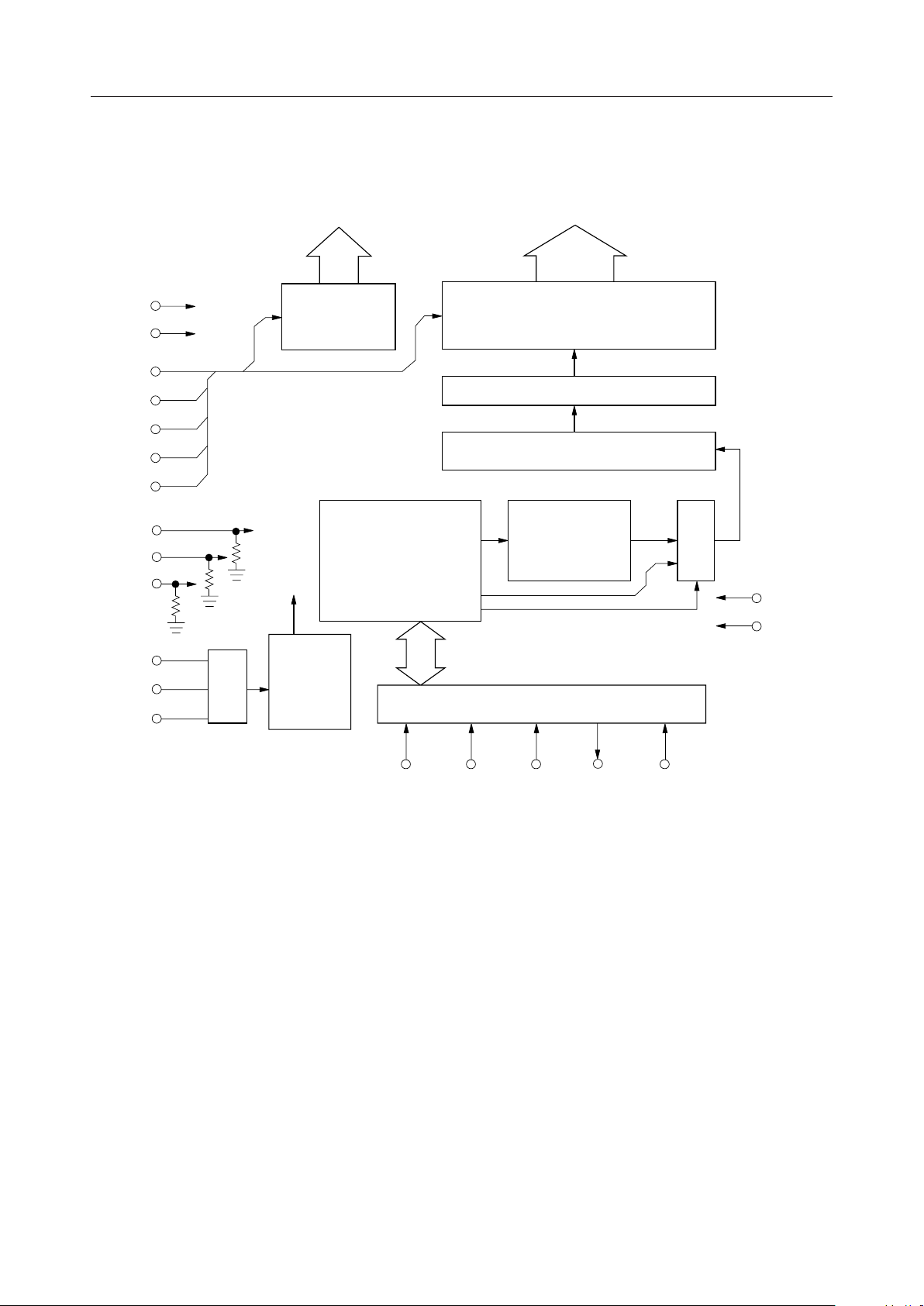
BLOCK DIAGRAM
V
DD
V
V
SS1
V
SS2
V
SS3
V
SS4
V
SS5
TEST1
TEST2
TEST3
OSC1
OSC2
OSC3
C1 - C17
17
COMMON
SS
DRIVER
S1 - S80
80
SEGMENT
DRIVER
LATCH
SHIFT REGISTER
RAM
CHARACTER
GENERATOR
ROM
F/F
GATE
(256x5x7dot)
(512-bit)
9D/
17D
RST
OSC
FREQUENCY
DIVIDER
&
TIMING
GENERATION
8
SERIAL/PARALLEL INTERFACE
CS C/ SHT SO SID
2/30
¡ Semiconductor MSM6665-xx
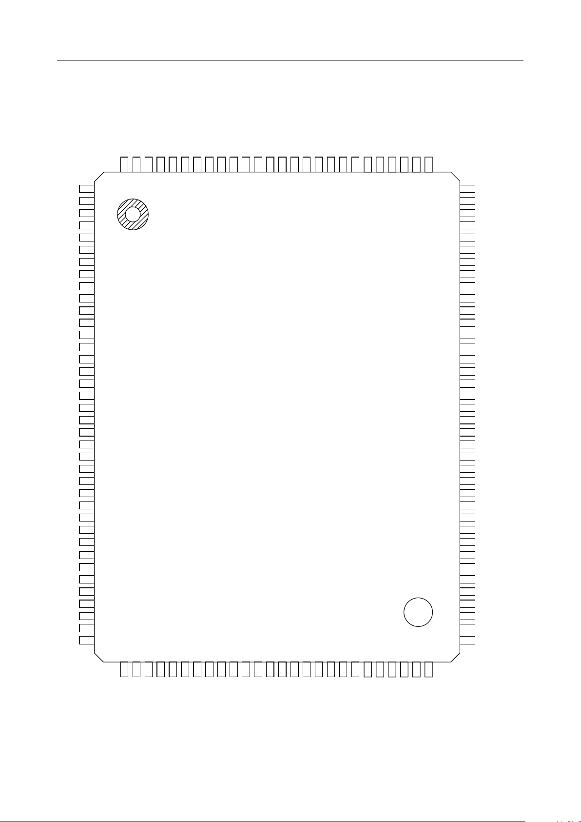
PIN CONFIGURATION (TOP VIEW)
S77
S76
S75
S74
S73
S72
S71
S70
S69
S68
S67
S66
S65
S64
S63
S62
S61
S60
S59
S57
S56
S55
S54
S53
S52
S51
S50
S49
S48
S47
S46
NC
S45
S44
NC
S43
S42
S41
S40
S39
S38
NC
S37
S36
NC
S35
S34
S33
S32
S31
S30
S29
S28
S27
S26
S25
S24
10
11
12
13
14
15
16
17
18
19
20
21
22
23
24
25
26
27
28
29
30
31
32
33
34
35
36
37
38
S58
109
110
111
112
113
114
115
116
117
118
119
120
121
122
123
124
125
126
127
128
1
2
3
4
5
6
7
8
9
S78
108
S79
107
S80
106
NC
105
TEST2
TEST3
103
104
102
TEST1
101
OSC3
100
OSC2
NC
99
OSC1
98
V
97
96
SO
95
RST
94
9D/17D
93
SHT
92
SI
91
C/D
90
NC
89
CS
88
V
87
NC
86
V
85
V
84
V
83
V
82
VSS (GND)
81
C1
80
NC
79
C2
78
C3
77
NC
76
C4
75
C5
74
C6
73
C7
72
C8
C9
71
C10
70
C11
69
C12
68
C13
67
C14
66
C15
65
DD
SS1
SS2
SS3
SS4
SS5
39
S23
40
S22
41
S21
42
S20
43
S19
44
S18
45
S17
51
50
49
48
47
46
S11
S12
S13
S14
S15
S16
NC : No connection
128-Pin Plastic QFP
52
S10
53
S9
54
S8
55
S7
56
S6
57
S5
58
S4
49
S3
60
S2
61
S1
62
C17
63
C16
64
NC
3/30
¡ Semiconductor MSM6665-xx
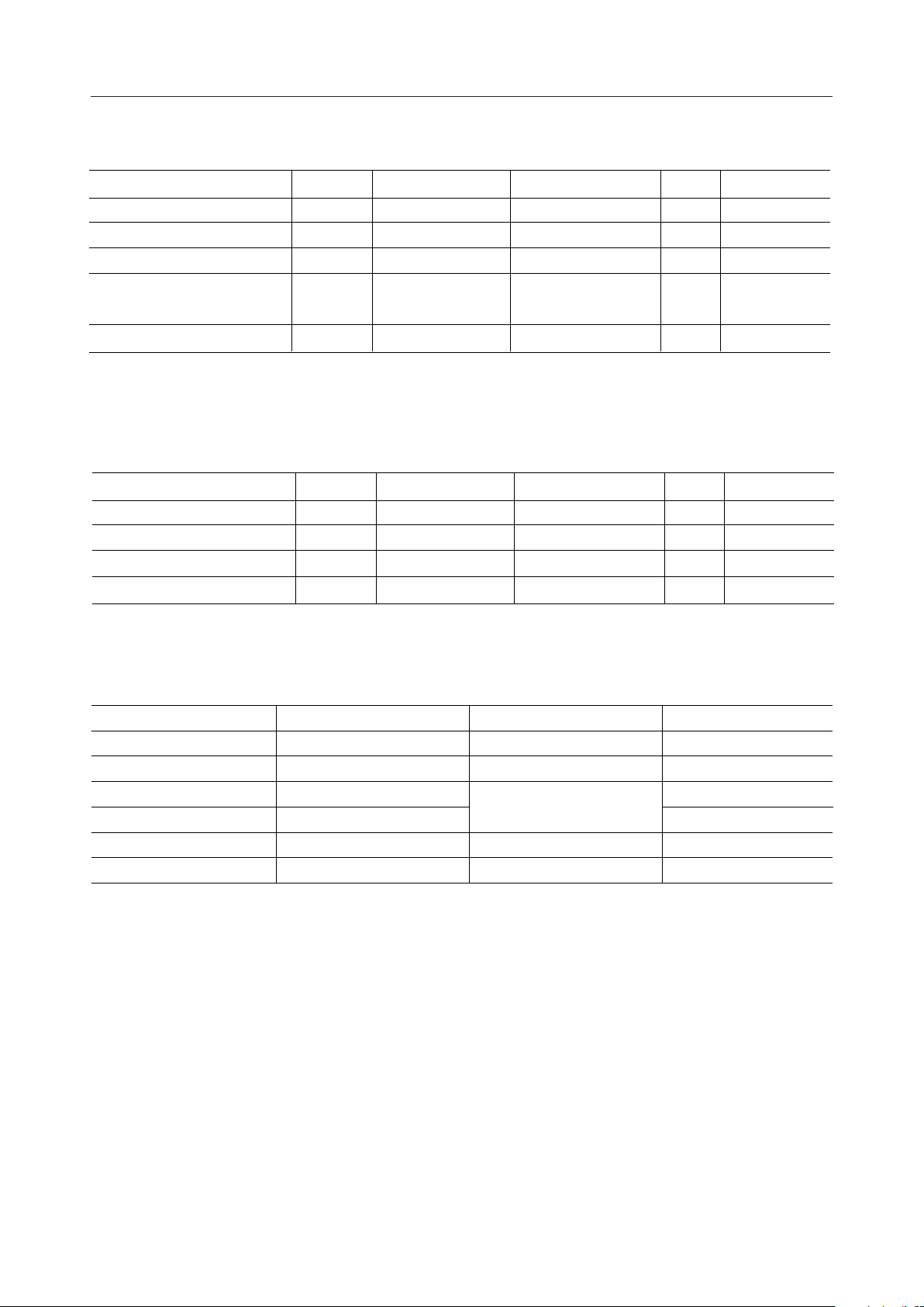
ABSOLUTE MAXIMUM RATINGS
Parameter UnitCondition
Supply Voltage
Bias Voltage Ta=25°C, V
Input Voltage
Power Dissipation
Storage Temperature
Symbol
V
DD
V
BI
V
I
P
D
T
STG
Ta=25°C, VDD–V
DD–VSS5
—
Ta=85°C
QFP128-1420
—
SS
*1
Rating Applicable pin
–0.3 to +7
–0.3 to +7 V VDD, V
–0.3 to V
DD
+0.3
630
–55 to +150
*1: The power dissipation depends on the heat sink characteristic of the package.
Set a junction temperature at 150°C or lower.
RECOMMENDED OPERATING CONDITIONS
Parameter UnitCondition
Supply Voltage
Bias Voltage V
Operating Frequency
Operating Temperature
*2: RC oscillation, external input clock frequency
Symbol
V
DD
V
BI
f
op
T
op
Rating Applicable pin
VDD–V
SS
DD–VSS5
*2
——
2.5 to 5.5
3 to 6 V VDD, V
65 to 115
–40 to +85
V
V
mW
°C
V
kHz
°C
V
, V
DD
SS
SS5
All inputs
—
—
, V
V
DD
SS
SS5
OSC1
List of bias voltages
Symbol
V
DD
V
SS1
V
SS2
V
SS3
V
SS4
V
SS5
1/5 bias
V
DD
VDD–1/5V
VDD–2/5V
VDD–3/5V
VDD–4/5V
V
SS5
(VBI=VDD–V
1/4 bias
V
DD
BI
BI
BI
BI
VDD–1/4V
VDD–2/4V
VDD–3/4V
V
SS5
BI
BI
BI
Remarks
Highest voltage
—
—
—
—
Lowest voltage
SS5
)
4/30
¡ Semiconductor MSM6665-xx
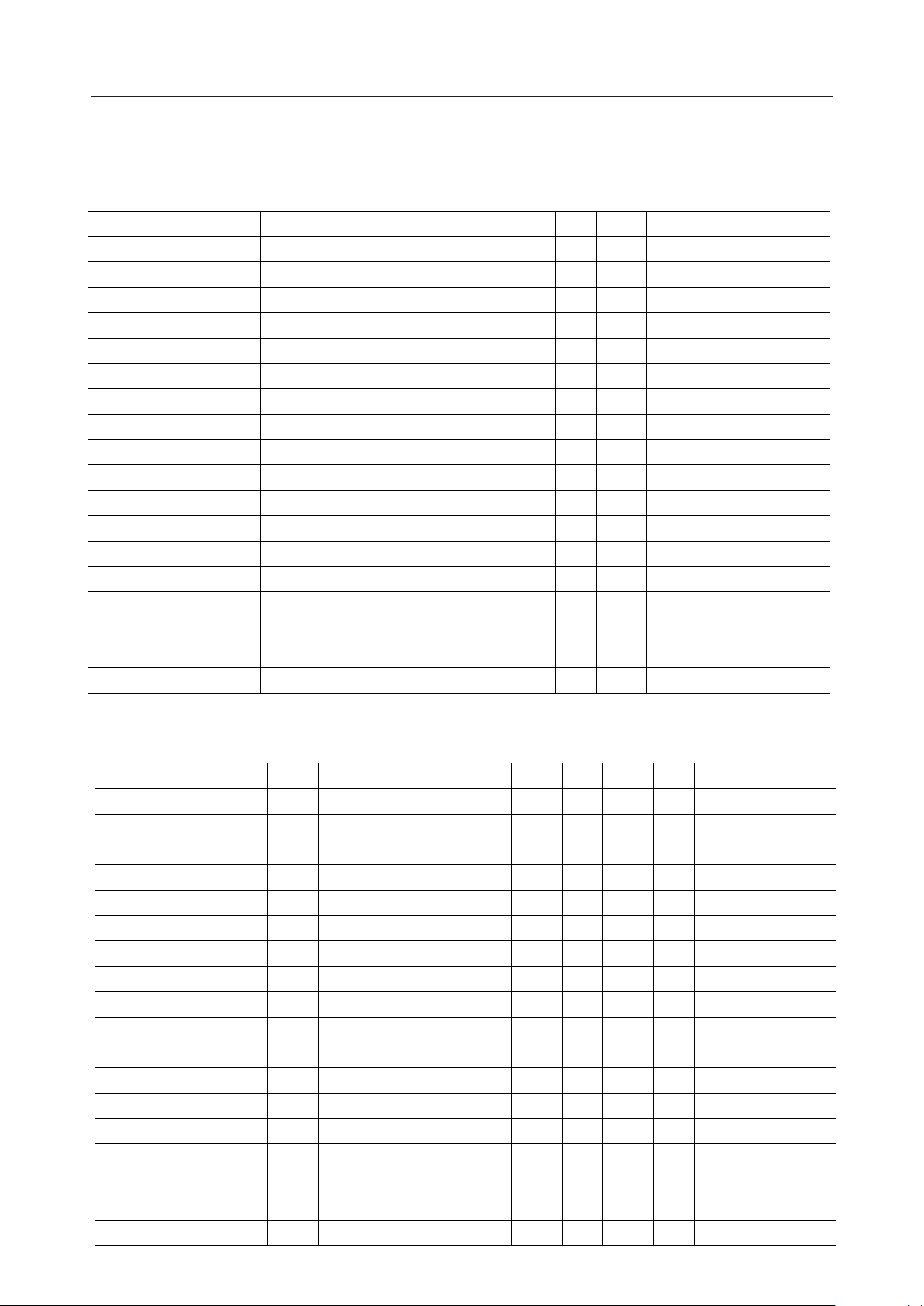
ELECTRICAL CHARACTERISTICS
DC Characteristics (1)
(V
=2.5 to 3.5V, VBI=3 to 6V, Ta=–40 to +85°C)
DD
Parameter
"H" Input Voltage 1
"L" Input Voltage 1
"H" Input Voltage 2
"L" Input Voltage 2
"H" Input Current 1
"L" Input Current
"H" Input Current 2
"H" Output Voltage
"L" Output Voltage
OFF Leakage
OSC "H" Output Current
OSC "L" Output Current
COM Output Resistance
SEG Output Resistance
Supply Current 1
Supply Current 2
Symbol
V
IH1
V
IL1
V
IH2
V
IL2
I
IH1
I
IL
I
IH2
V
OH
V
OL
I
OFF
I
OH
I
OL
R
C
R
S
I
DD1
I
DD2
Condition Min. Typ. Max. Unit Applicable pin
External clock input
External clock input
—
—
V
I=VDD
VI=0V
Pull-down resistance, V
IO=–1.5mA
I
=500mA
O
/0V
V
I=VDD
–0.5V
V
I=VDD
=0.5V
V
I
I
=±50mA
O
=±10mA
I
O
RC oscillation, f=80kHz
C=56pF, R
=10kW
S
.
.
R=76kW, no load
External clock, f=80kHz
I=VDD
0.8V
0.8V
—VDDV OSC1
DD
0 — 0.2V
—VDDV
DD
0 — 0.2V
DD
DD
V OSC1
V
—— 1 mA
Input pins except OSC1
Input pins except OSC1
Input pins except TEST
——–1mA Input pins
0.05 — 0.4 mA TEST1-TEST3
VDD–0.5
—— VS0
— — 0.5 V S0
——±1mAS0
— — –0.25 mA OSC2, OSC3
0.25 — — mA OSC2, OSC3
—— 6kW C1-C17
——15kW S1-S80
— — 0.5 mA —
— — 100 mA—
DC Characteristics (2)
Parameter
"H" Input Voltage 1
"L" Input Voltage 1
"H" Input Voltage 2
"L" Input Voltage 2
"H" Input Current 1
"L" Input Current
"H" Input Current 2
"H" Output Voltage
"L" Output Voltage
OFF Leakage
OSC "H" Output Current
OSC "L" Output Current
COM Output Resistance
SEG Output Resistance
Supply Current 1
Supply Current 2
Symbol
V
IH1
V
IL1
V
IH2
V
IL2
I
IH1
I
IL
I
IH2
V
OH
V
OL
I
OFF
I
OH
I
OL
R
C
R
S
I
DD1
I
DD2
Condition Min. Typ. Max. Unit Applicable pin
External clock input
External clock input
—
—
V
I=VDD
VI=0V
Pull-down resistance, V
IO=–1.5mA
=500mA
I
O
V
/0V
I=VDD
–0.5V
V
I=VDD
=0.5V
V
I
=±50mA
I
O
I
=±10mA
O
RC oscillation, f=80kHz
C=56pF, R
=10kW
S
.
.
R=76kW, no load
External clock, f=80kHz
I=VDD
(V
=4.5 to 5.5V, VBI=3 to 6V, Ta=–40 to +85°C)
DD
0.8V
0.8V
—VDDV OSC1
DD
0 — 0.2V
—VDDV
DD
0 — 0.2V
DD
DD
V OSC1
V
—— 1 mA
Input pins except OSC1
Input pins except OSC1
Input pins except TEST
——–1mA Input pins
0.3 — 1.4 mA TEST1-TEST3
VDD–0.5
—— VS0
— — 0.5 V S0
——±1mAS0
— — –0.5 mA OSC2, OSC3
0.5 — — mA OSC2, OSC3
—— 6kW C1-C17
——15kW S1-S80
— — 1.1 mA —
— — 400 mA—
5/30
¡ Semiconductor MSM6665-xx
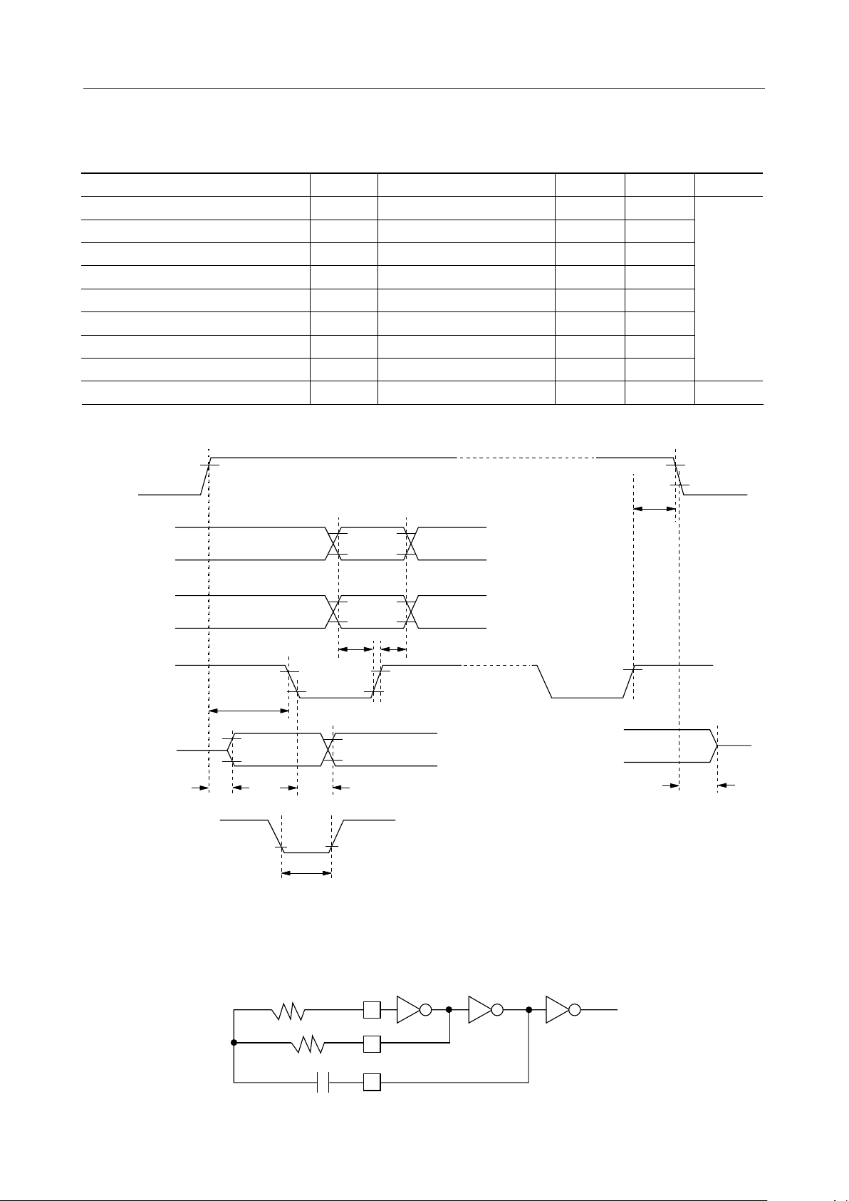
AC Characteristics
Parameter
CS Setup Time
CS Hold Time
SO ON Delay Time
SO OFF Delay Time
SO Output Delay Time
Input Setup Time
Input Hold Time
Input Waveform Rise Time, Fall Time
Reset Pulse Input Pulse Width
CS
SI
Symbol Condition
t
t
t
t
t
t
t
CS
CH
ON
OFF
DLY
t
IS
t
IH
r, tf
RT
CL=45pF
All inputs
—
—
—
—
—
—
—
V
IH2
V
IL2
(V
DD–VSS
=2.5 to 5.5V, Ta=–40 to +85°C)
Min.
300
200
—
—
0
200
200
—
5
Max.
—
—
200
200
200
—
—
50
—
t
CH
Unit
ns
µs
V
IH2
V
IL2
C/
D
SHT
SO
"Z"
t
ON
RST
Oscillation Circuit
V
IH2
V
IL2
t
IS
t
CS
V
OH
V
OL
t
DLY
V
t
RT
R
S
IL2
OSC1
t
IH
V
IH2
V
IL2
"Z"
t
OFF
*
V
=0.8V
IH2
V
IL2
=0.2V
DD
DD
VOH=VDD–0.5V
=0.5V
V
OL
R
OSC2
OSC3
C
6/30
¡ Semiconductor MSM6665-xx
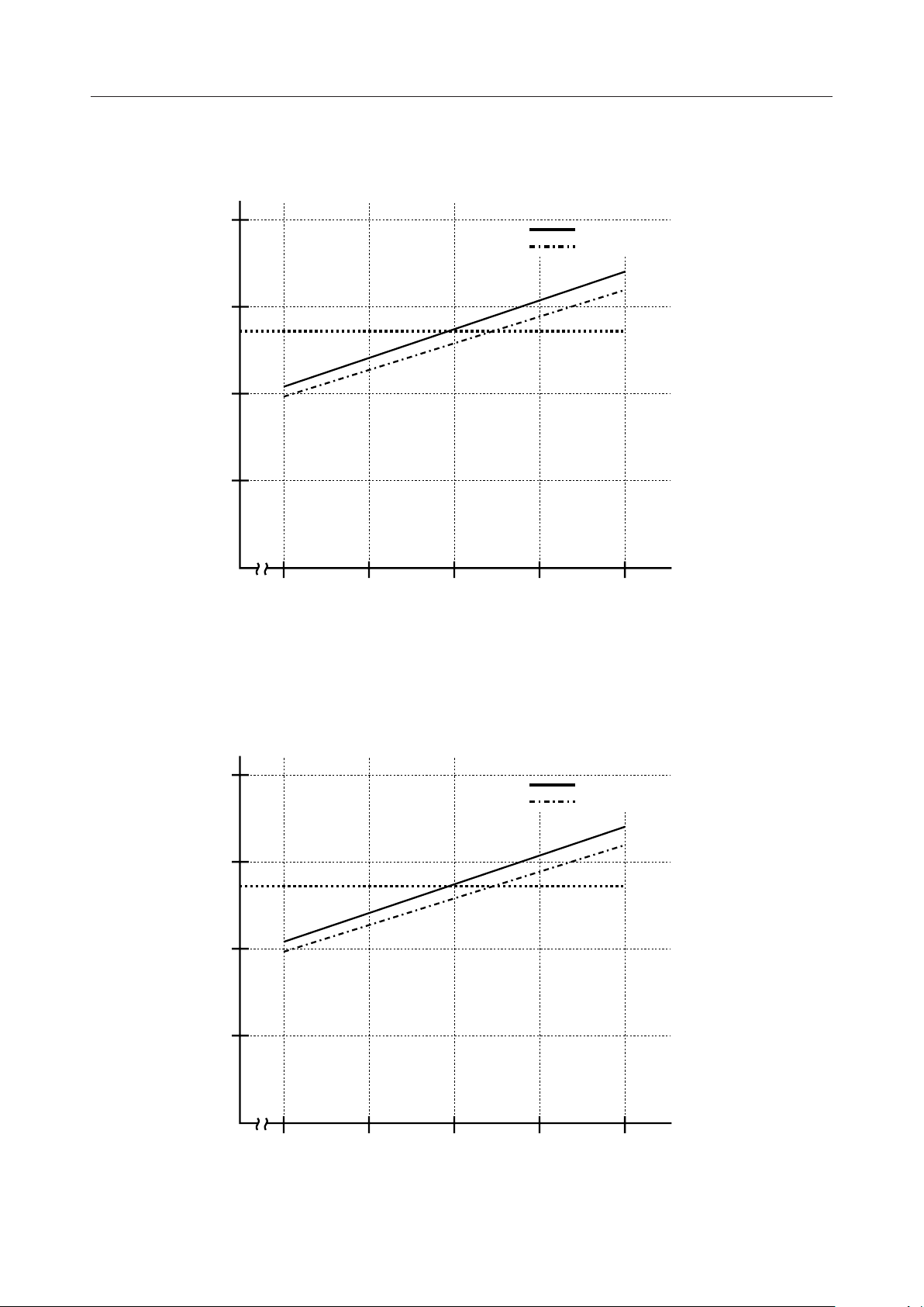
Oscillation Characteristics 1 (Rs=10kW, C=56pF, R variable characteristics)
1/17 duty
Frame Cycle¥2 (ms)
40
30
20
10
VDD =3.0V
V
=5.0V
DD
f=80kHz,
Frame cycle¥2=27.2ms
0
55 65 75 85 95
R Resistance (k )
W
Oscillation Characteristics 2 (Rs=10kW, R=75kW, C variable characteristics)
1/17 duty
40
30
20
Frame Cycle¥2 (ms)
10
0
VDD =3.0V
V
=5.0V
DD
f=80kHz,
Frame cycle¥2=27.2ms
35 45 55 65 75
C Capacitance (pF)
7/30

¡ Semiconductor MSM6665-xx
FUNCTIONAL DESCRIPTION
Pin Functional Description
• SI (Serial Input)
Input pin for inputting serially commands and display data in an 8-bit unit.
"H"="1" and "L"="0".
When CS pin is at "H" level, read-in is executed by the leading edge of SHT.
Whether input data is a command or data is determined by selecting a C/D level at the
8th leading edge of SHT.
The input data is a command if C/D="H", and display data if C/D="L".
•C/D (Command/Data)
Input pin for determining whether input data for SI pin is a command or display data.
Read-in is executed by the 8th leading edge of SHT. The input data is a command if C/
D="H", and display data if C/D="L".
• SHT (Shift Clock)
Clock input pin for reading-in SI input and C/D input.
Read-in is executed by the clock leading edge. Read-in operation is complete with 8
clocks. Inputting data during BUSY may cause malfunction.
Valid if CS pin is at "H" level.
• SO (Serial Out)
Serial output pin for reading-out BUSY/NON-BUSY and display data. "H"="1" and
"L"="0". If CS pin is at "H" level and Serial Out Enable is set with the command, output
is executed. Otherwise, this pin becomes high impedance.
BUSY/NON-BUSY is output when CS pin is at "H" level. BUSY if "L" and NON-BUSY
if "H". It goes BUSY after the 8th leading edge of SHT, then goes NON-BUSY
automatically after a specified time.
Display data is output synchronously with the leading edge of SHT.
Input the "SOE/D" instruction to set this output to serial out enable or a high impedance
state because the pin status is undefined after the power is applied.
• CS (Chip Select)
Chip Select input pin.
"Chip Select ON" if CS pin is at "H" level, and "Chip Select OFF" at "L" level. When "L"
level is input, SO pin becomes open and SHT pin becomes equivalent to "H" level inside
of the IC. Moreover, it prevents the input stages of SI, C/D and SHT pins from current
flowing.
* For SI, C/D, SHT, SO, and CS, refer to "I/O Procedure".
• RST
Direct input reset input pin.
By inputting "L" level pulse into RST pin, DISP, ABBC1/5, ABB, and BPC commands are
set as D0="0". Before turning on the power, be sure to set RST pin at "L" level once. Setting
this pin at "L" level during command execution may cause malfunction.
• 9D/17D (1/9Duty/1/17Duty)
Duty setting input pin.
1/9 duty is set if this pin is at "H" level, and 1/17 duty at "L" level. Choice depends on
the type of panel to be used.
8/30
¡ Semiconductor MSM6665-xx
If 1/9 duty is selected, common outputs C10 to C17 should be set open.
• TEST1, TEST2, TEST3
Test signal input pins.
The manufacturer uses these pins for testing.
The user should connect this pin to GND or leave open.
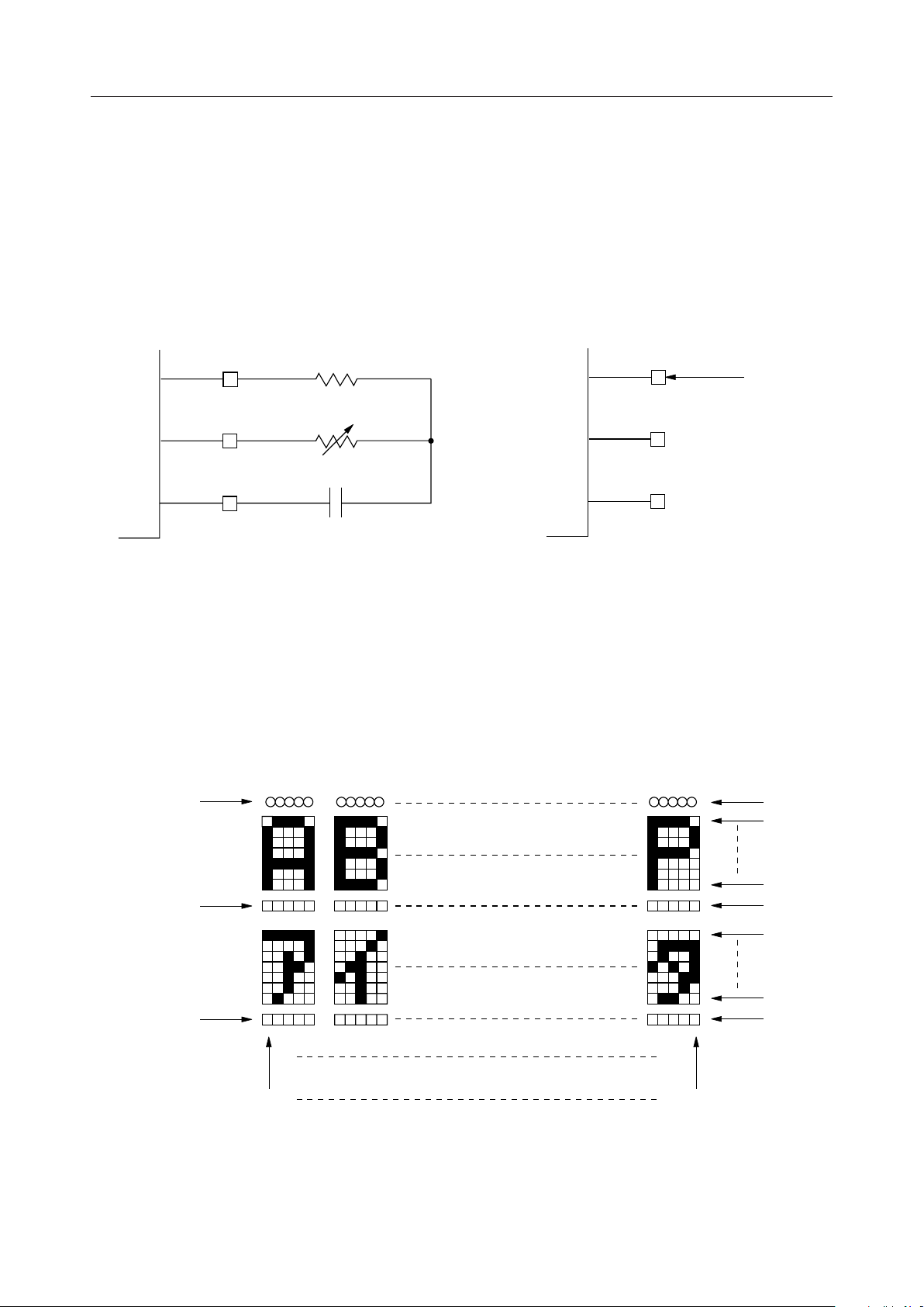
• OSC1, OSC2, OSC3
Pins used for 80kHz RC oscillation circuit formation and as external master clock input
pin. Leave OSC2 and OSC3 open during input of external master clock.
10k
76±5k
56pF
W
W
OSC1
OSC2
OSC3
< Oscillation circuit wiring diagram >
• C1 - C17, S1 - S80 (Common 1 - 17, Segment 1 - 80)
LCD output pins to be connected with the LCD panel. Turning into AC is made by frame
inversion.
Use the C1 to C9 pins during use at 1/9 duty, and leave the C10 to C17 pins open.
ÆRefer to "Relationship between panel and LCD output".
Arbitrator
OSC1
80kHz
OSC2
OPEN
OSC3
OPEN
[External master clock input][RC oscillation circuit formation]
C1
C2
Cursor
Cursor
•VDD, V
Supply voltage pins. VDD should be set at "H" level.
C8
C9
C10
C16
C17
S1 S80
<Relationship between panel and LCD output>
SS
9/30
 Loading...