

Page 1
D
ATA SHEET
O K I COMMUNICATIONS P R O D U C T S
MBF93xx
Surface Acoustic Wave (SAW) Filters
for Mobile and Portable Phones
September 1997
Page 2

■ MBF93xx■ ––––––––––––––––––––––––––––––––––––––––––––––––––––––––––––––––––––––––––––––––––––
Oki Semiconductor
Page 3
MBF93xx
Surface Acoustic Wave (SAW) Filters
DESCRIPTION
The new MBF93xx Surface Acoustic Wave (SAW) filters use Oki’s third generation design and manufacturing technology to achieve a high out-of-band attenuation, low insertion loss, and low manufacturing
cost in an industry standard 6-pin package, 1.6-mm thick and 3.8-mm square.
These 50-Ω matched bandpass microwave RF filters are designed for the worldwide standard wireless
voice and data communications frequencies being used by cellular and wireless local-loop service providers. They have achieved design acceptance by leading wireless handset manufacturers in North
America, Europe, and Asia.
Oki’s lowest insertion loss SAW filters and high performance GaAs devices are used to reduce transmitter complexity. Receiver designs can be simplified by using the higher Tx frequency attenuation SAW
filters.
These devices take advantage of Oki’s 15-year plus RF communications component manufacturing experience and very high volume manufacturing capability to meet true customer demands.
FEATURES
• Low insertion loss
• Small size, light weight
• 50-Ω matched
• 6-pin SMD package
• High reliability
SAW Filter Summary
Part
Number
MBF9311 CDMA, AMPS, & TDMA Receive filter for North America standards 869 to 894 <3.0 824 to 849 >35
MBF9317 CDMA, AMPS, & TDMA Transmit filter for North America standards 824 to 849 <3.5 869 to 894 >30
MBF9321 GSM Transmit filter for European standards 890 to 915 <3.5 935 to 980 >20
MBF9323 GSM Receive filter for European standards 935 to 960 <4.0 890 to 915 >20
MBF9332 ETACS Receive filter for world wide ETACS standard 917 to 950 <5.0 872 to 900 >25
MBF9361B PCS, CDMA, & TDMA Transmit filter for North America standards 1850 to 1910 <5.0 1930 to 1990 >18
MBF9362B PCS, CDMA, & TDMA Receive filter for North America standards 1930 to 1990 <5.0 1850 to 1910 >20
1. All parts in 6-pin ceramic square package (3.8 mm x 3.8 mm) by 1.6-mm thick with system matched 50-Ω I/O
[1]
Description
Pass Frequency
(MHz)
Insertion
Loss (dB)
Stop Frequency
(MHz)
Attenuation
(dB)
1Oki Semiconductor
Page 4
■ MBF93xx ■ –––––––––––––––––––––––––––––––––––––––––––––––––––––––––––––––––––––––––––––––––––
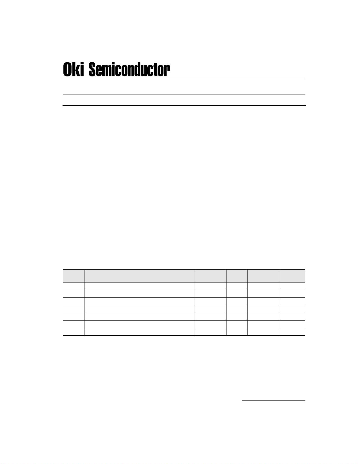
PIN CONFIGURATION
3.8 ±0.2
3.8 ±0.2
BLOCK DIAGRAM
Ant
DUPLEXER
Rx-BPF
Tx-BPF
1.6
Power Amp
0.6
1 2 3
1.9
6 5 4
1.27 1.27
Rx-BPF
SAWRF Amp
SAW
Tx-BPF
VCO
IF-BPF
Mixer
RF Amp Mixer
Pin Number Signal
1.0
IF Amp
1, 3, 4, 6 Ground
2 Input
5 Output
DEMO
MOD
2 Oki Semiconductor
VCO
Page 5
–––––––––––––––––––––––––––––––––––––––––––––––––––––––––––––––––––––––––––––––––– ■ MBF93xx ■
MBF9311 Electrical Characteristics (-30 to +85°C)
Parameter Frequency (MHz) Min. Max. Units
Center Frequency (FC) Fr 881.5 – – MHz
Bandwidth (BW) Fr ±12.5 – – MHz
Insertion Loss across BW
Return Loss across BW 10 – dB
869–894
Stop Band Attenuation 0.3 to 824 20 – dB
824 to 849 35 – dB
979 to 1004 25 – dB
1008 to 1114 20 – dB
Terminating Impedance = 50 Ω
CH1
S
log MAG
11
CH2
S
log MAG
21
CDMA R–INT
1
Cor
Hld
Cor
Hld
START 760.000 000 MHz STOP 960.000 000 MHz
5 dB/
REF0db
10 dB/
REF0db
1
3
4
1
3
4
– 3.0 dB
1. –12.648 dB
1. –2.5314 dB
869.000 000 MHz
2. –16.655 dB
2
2
894 MHz
3. –.8658 dB
824 MHz
4. –1.5369 dB
849 MHz
PASS
2. –2.1717 dB
894 MHz
3. –42.869 dB
824 MHz
4. –52.859 dB
849 MHz
PASS
2
Figure 1. MBF9311 Frequency Response
3Oki Semiconductor
Page 6

■ MBF93xx ■ –––––––––––––––––––––––––––––––––––––––––––––––––––––––––––––––––––––––––––––––––––
MBF9317 Electrical Characteristics (-30 to +85°C)
Parameter Frequency (MHz) Min. Max. Units
Center Frequency (FC) Ft 836.5 – – MHz
Bandwidth (BW) Fr ±12.5 – – MHz
Insertion Loss across BW 824 to 849 – 3.5 dB
Return Loss across BW 10.0 – dB
Stop Band Attenuation 0.3 to 800 28 – dB
869 to 1049 30 – dB
1049 to 2000 25 – dB
Terminating Impedance = 50 Ω
CH1
S
CH2
Cor
Hld
11
S
21
CDMA TX
1
log MAG
log MAG
5 dB/
REF0db
10 dB/
REF0db
1
2
1
4
3
1. –13.521 dB
1. –2.5218 dB
824.000 000 MHz
2. –18.22 dB
849 MHz
3. –2.0714 dB
869 MHz
4. –1.2669 dB
894 MHz
Cor
Hld
CENTER 860.000 000 MHZ SPAN 200.000 000 MHZ
4 Oki Semiconductor
2
4
3
2. –2.5311 dB
849 MHz
3. –42.717 dB
869 MHz
4. –41.694 dB
894 MHz
Figure 2. MBF9317 Frequency Response
2
Page 7

–––––––––––––––––––––––––––––––––––––––––––––––––––––––––––––––––––––––––––––––––– ■ MBF93xx ■
MBF9321 Electrical Characteristics (-30 to +85°C)
Parameter Frequency (MHz) Min. Max. Units
Center Frequency (FC) 902.5 – – MHz
Bandwidth (BW) Ft ±12.5 – – MHz
Insertion Loss across BW
Ripple across BW – 2.0 dB
890 to 915
VSWR across BW – 2.5 –
Stop Band Attenuation 500 to 870 20 – dB
935 to 980 20 – dB
980 to 1100 26 – dB
1100 to 1500 15 – dB
Terminating Impedance = 50 Ω
– 3.5 dB
CH1
S
log MAG
11
CH2
S
log MAG
21
MBF9321
1
Cor
Hld
Cor
Hld
START 825.000 000 MHZ STOP 1 025.000 000 MHZ
5 dB/
REF0db
10 dB/
REF0db
1
2
3
1
2
3
890.000 000 MHz
4
4
2. –2.811 dB
3. –41.435 dB
4. –41.396 dB
Figure 3. MBF9321 Frequency Response
1. –.14.793 dB
1. –2.5312 dB
2. –17.95 dB
915 MHz
3. –2.194 dB
935 MHz
4. –.6314 dB
960 MHz
915 MHz
935 MHz
960 MHz
2
5Oki Semiconductor
Page 8

■ MBF93xx ■ –––––––––––––––––––––––––––––––––––––––––––––––––––––––––––––––––––––––––––––––––––
MBF9323 Electrical Characteristics (-30 to +85°C)
Parameter Frequency (MHz) Min. Max. Units
Center Frequency (FC) 947.5 – – MHz
Bandwidth (BW) Ft ±12.5 – – MHz
Insertion Loss across BW
Ripple across BW – 2.0 dB
935 to 960
VSWR across BW – 2.5 –
Stop Band Attenuation 500 to 870 30 – dB
890 to 915 20 – dB
980 to 1025 15 – dB
1025 to 1070 33 – dB
1070 to 1105 30 – dB
1105 to 1500 20 – dB
Terminating Impedance = 50 Ω
– 3.5 dB
CH1
S
log MAG
11
CH2
S
log MAG
21
GSM R-INT
1
Cor
Hld
Cor
Hld
CENTER 925.000 000 MHZ SPAN 200.000 000 MHZ
5 dB/
REF0db
10 dB/
REF0db
1
3
4
1
4
3
935.000 000 MHz
2
2
Figure 4. MBF9323 Frequency Response
1. –14.701 dB
1. –2.8949 dB
2. –16.418 dB
960 MHz
3. –.7898 dB
890 MHz
4. –1.2104 dB
915 MHz
2. –2.4335 dB
960 MHz
3. –36.589 dB
890 MHz
4. –28.192 dB
915 MHz
2
6 Oki Semiconductor
Page 9

–––––––––––––––––––––––––––––––––––––––––––––––––––––––––––––––––––––––––––––––––– ■ MBF93xx ■
MBF9332 Electrical Characteristics (-30 to +85°C)
Parameter Frequency (MHz) Min. Max. Units
Center Frequency (FC) 933.5 – – MHz
Bandwidth (BW) Ft ±16.5 – – MHz
Insertion Loss across BW
VSWR across BW – 2.0 –
917 to 950
Stop Band Attenuation 0 to 872 20 – dB
872 to 900 25 – dB
900 to 905 10 – dB
1007 to 1040 30 – dB
1040 to 2000 20 – dB
Output Reflection Coefficient Mag
Angle -155 -125 Degrees
1031 to 1065
Terminating Impedance = 50 Ω
– 5.5 dB
0.86 Degrees
CH1
S
log MAG
11
CH2
S
log MAG
21
E–TACS R–INT
MBF9332/E01
1
Cor
Hld
Cor
Hld
CENTER 910.000 000 MHZ SPAN 200.000 000 MHZ
5 dB/
10 dB/
REF0db
REF0db
1
3
1
3
917.000 000 MHz
2
4
4
2
Figure 5. MBF9332 Frequency Response
1. –17.258 dB
1. –3.8643 dB
2. –22.767 dB
950 MHz
3. –1.5338 dB
905 MHz
4. –12.132 dB
924 MHz
2. –3.0037 dB
950 MHz
3. –28.311 dB
905 MHz
4. –2.7303 dB
924 MHz
2
7Oki Semiconductor
Page 10

■ MBF93xx ■ –––––––––––––––––––––––––––––––––––––––––––––––––––––––––––––––––––––––––––––––––––
MBF9361B Electrical Characteristics (-30 to +85°C)
Parameter Frequency (MHz) Min. Typ. Max. Units
Center Frequency (FC) 1880 – – – MHz
Bandwidth (BW) Ft ±30 – – – MHz
Insertion Loss across BW
Ripple across BW – 2.0 – dB
1850 to 1910
VSWR across BW – – 2.0 –
Stop Band Attenuation 1590 to 1650 18 – – dB
1720 to 1780 16 – – dB
1930 to 1990 7 14 – dB
Terminating Impedance = 50 Ω
CH1
S
CH2
Cor
Hld
11
S
21
PCS TX
MBF9341
1
log MAG
log MAG
1
1
5 dB/
10 dB/
REF0db
REF0db
2
3
3
– – 5.0 dB
1. –13.585 dB
1. –1.8686 dB
1 850.000 000 MHz
2. –21.065 dB
4
4
1.91 GHz
3. –6.5681 dB
1.93 GHz
4. –1.659 dB
1.99 GHz
2
Cor
Hld
CENTER 1 920.000 000 MHZ SPAN 300.000 000 MHZ
8 Oki Semiconductor
2
2. –3.3965 dB
1.91 GHz
3. –18.145 dB
1.93 GHz
4. –26.101 dB
1.99 GHz
Figure 6. MBF9361B Frequency Response
Page 11

–––––––––––––––––––––––––––––––––––––––––––––––––––––––––––––––––––––––––––––––––– ■ MBF93xx ■
MBF9362B Electrical Characteristics (-30 to +85°C)
Parameter Frequency (MHz) Min. Typ. Max. Units
Center Frequency (FC) Fr: 1960 MHz
Bandwidth (BW) Fr± 30 MHz
Insertion Loss across BW
Ripple across BW – 2.0 3.0 dB
1930 to 1990
VSWR across BW – – 2.0 –
Stop Band Attenuation 1509 to 1570 20 – – dB
1720 to 1780 20 – – dB
1850 to 1910 13 26 – dB
Terminating Impedance = 50 Ω
S
CH1
CH2
Cor
Hld
11
S
21
PCS RX
MBF9342
1
log MAG
log MAG
5 dB/
REF0db
10 dB/
REF0db
1
3
2
– – 5.0 dB
1. –24.341 dB
1. –3.3474 dB
1 930.000 000 MHz
2. –21.733 dB
4
1.99 GHz
3. –1.0473 dB
1.85 GHz
4. –2.5575 dB
1.91 GHz
2
3
Cor
Hld
CENTER 1 920.000 000 MHZ SPAN 300.000 000 MHZ
4
1
2
2. –2.0629 dB
3. –34.113 dB
4. –31.687 dB
Figure 7. MBF9362B Frequency Response
1.99 GHz
1.85 GHz
1.91 GHz
9Oki Semiconductor
Page 12

■ MBF93xx ■ –––––––––––––––––––––––––––––––––––––––––––––––––––––––––––––––––––––––––––––––––––
Notes:
10 Oki Semiconductor
Page 13

–––––––––––––––––––––––––––––––––––––––––––––––––––––––––––––––––––––––––––––––––– ■ MBF93xx ■
Notes:
11Oki Semiconductor
Page 14

■ MBF93xx ■ –––––––––––––––––––––––––––––––––––––––––––––––––––––––––––––––––––––––––––––––––––
12 Oki Semiconductor
Page 15

The information contained herein can change without notice owing to product and/or technical improvements.
Please make sure before using the product that the information you are referring to is up-to-date.
The outline of action and examples of application circuits described herein have been chosen as an explanation of the standard action
and performance of the product. When you actually plan to use the product, please ensure that the outside conditions are reflected in
the actual circuit and assembly designs.
Oki assumes no responsibility or liability whatsoever for any failure or unusual or unexpected operation resulting from misuse, neglect,
improper installation, repair, alteration or accident, improper handling, or unusual physical or electrical stress including, but not limited
to, exposure to parameters outside the specified maximum ratings or operation outside the specified operating range.
Neither indemnity against nor license of a third party's industrial and intellectual property right,etc.is granted by us in connection with
the use of product and/or the information and drawings contained herein. No responsibility is assumed by us for any infringement of a
third party's right which may result from the use thereof.
When designing your product, please use our product below the specified maximum ratings and within the specified operating ranges,
including but not limited to operating voltage, power dissipation, and operating temperature.
The products listed in this document are intended for use in general electronics equipment for commercial applications (e.g.,office
automation, communication equipment, measurement equipment, consumer electronics, etc.).These products are not authorized for
use in any system or application that requires special or enhanced quality and reliability characteristics nor in any system or application
where the failure of such system or application may result in the loss or damage of property or death or injury to humans. Such
applications include, but are not limited to: traffic control, automotive, safety, aerospace, nuclear power control, and medical, including
life support and maintenance.
Certain parts in this document may need governmental approval before they can be exported to certain countries. The purchaser
assumes the responsibility of determining the legality of export of these parts and will take appropriate and necessary steps, at their
own expense, for export to another country.
Copyright 1997 Oki Semiconductor
Oki Semiconductor reserves the right to make changes in specifications at anytime and without notice. This information furnished by
Oki Semiconductor in this publication is believed to be accurate and reliable. However, no responsibility is assumed by OKI
Semiconductor for its use; nor for any infringements of patents or other rights of third parties resulting from its use. No license is
granted under any patents or patent rights of OKI.
Oki Semiconductor
Page 16

Oki R
EGIONAL SALES
O
FFICES
Northwest Area
785 N. Mary Avenue
Sunnyvale, CA 94086
Tel: 408/720-8940
Fax: 408/720-8965
Southwest Area
2302 Martin Street
Suite 250
Irvine, CA 92715
Tel: 714/752-1843
Fax: 714/752-2423
North Central Area
17177 N. Laurel Park Drive
Suite 433
Livonia, MI 48152
Tel: 313/464-7200
Fax: 313/464-1724
South Central Area
2007 N. Collins Blvd.
Suite 303
Richardson, TX 75080
Tel: 214/690-6868
Fax: 214/690-8233
Northeast Area
138 River Road
Shattuck Office Center
Andover, MA 01810
Tel: 508/688-8687
Fax: 508/688-8896
Southeast Area
1590 Adamson Parkway
Suite 220
Morrow, GA 30260
Tel: 404/960-9660
Fax: 404/960-9682
Oki Web Site:
http://www.okisemi.com
Oki FAX Service:
Call toll free 1-800-OKI-6994
Oki Stock No:
090570-004
Corporate Headquarters
785 N. Mary Avenue
Sunnyvale, CA 94086-2909
Tel: 408/720-1900
Fax: 408/720-1918
 Loading...