

Page 1
Y
OKI Semiconductor
MBF9042BB
SAW Antenna Duplexer (700 to 1000 MHz)
GENERAL DESCRIPTION
The MBF9042BB is the SAW antenna duplexer for the frequency range of 700 to 1000 MHz.
This SAW Duplexer integrates RF filters at Tx and Rx side, and matching circuit into PKG. This helps to save the
space and weight greatly in the target application such as mobile telephone.
This SAW Duplexer has very low insertion loss by using high quality pack age.
Due to high harmonics characteristics, total number of components at RF circuit can be minimized.
Thanks to high isolation performance, high sensitivity can be expected. Low insertion loss at Tx saves the power
consumption of mobile telephone which prolong the battery life.
FEATURES
• Complying Standard AMPS, IS-95, IS-136
• Thin package: less than 1.5 mm in height
• PKG I/O Impedance: 50 Ω
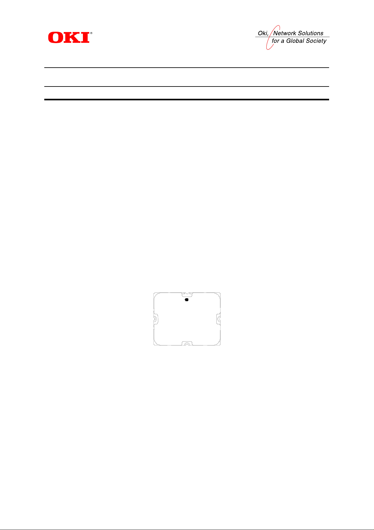
PRODUCT DESCRIPTION
Package Type
MBF9042BB
Rx
ANT
OKI
042BB
ZZZ
Tx
FEDW9042BB-02
Issue Date: May 20, 2002
1/11
Page 2
FEDW9042BB-02
Y
Semiconductor
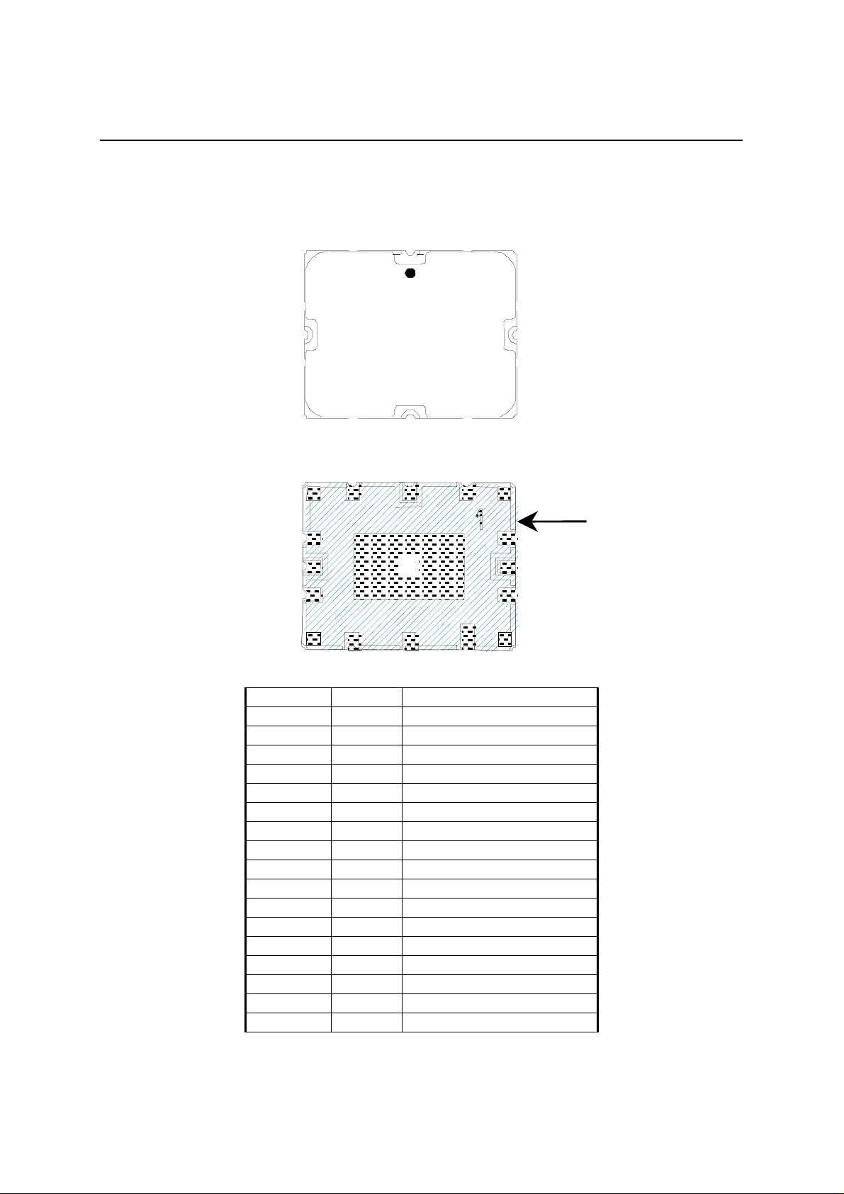
PIN ASSIGNMENT & DESCRIPTION
(12)
(13)
(14)
(15)
(16)
(16)
(15)
(14)
(13)
(12)
Pin No. Name Description
1 GND Ground Pin
2 ANT Antenna Pin
3 GND Ground Pin
4 GND No Connection *
5 GND Ground Pin
6 Tx Transmitting Terminal Pin
7 GND Ground Pin
8 GND No Connection *
9 GND Ground Pin
10 GND Ground Pin
11 GND Ground Pin
12 GND No Connection *
13 GND Ground Pin
14 Rx Receiving Terminal Pin
15 GND Ground Pin
16 GND No Connection *
17 GND Ground Pin
Note) Pin No. 4, 8, 12 and 16 are for manufacturer’s internal
use. Do not solder to the PCB.
(11)
042BB
(1)
(1)
(11)
Top view
(10)
OKI
ZZZ
(2) (3)
Bottom view
(2)
(17)
(10)
(3)
(9)
(9)
(4)
(8)
(8)
(7)
(6)
(5)
(4)
(5)
(6)
(7)
MBF9042BB
This number is for OKI
production purpose only.
2/11
Page 3
FEDW9042BB-02
Semiconductor
MBF9042BB
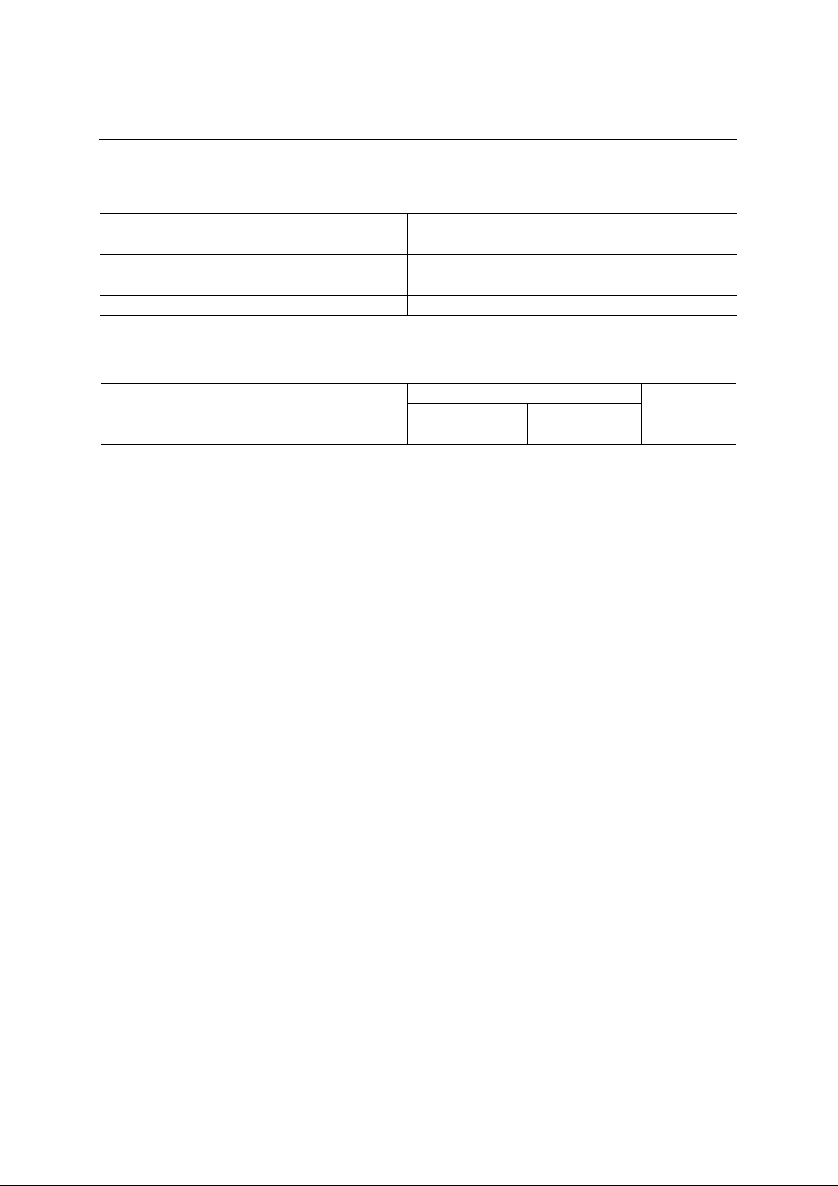
ABSOLUTE MAXIMUM RATINGS
Parameter Symbol
Operating Temperature Ta –30 +85 °C
Storage Temperature T
Maximum Input Power PIN — 2.0 W
–40 +85 °C
STG
Min. Max.
Rating
Unit
RECOMMENDED OPERATING CONDITIONS
Parameter Symbol
Operating Temperature Ta –30 +85 °C
Min. Max.
Rating
Unit
3/11
Page 4
FEDW9042BB-02
Semiconductor
MBF9042BB
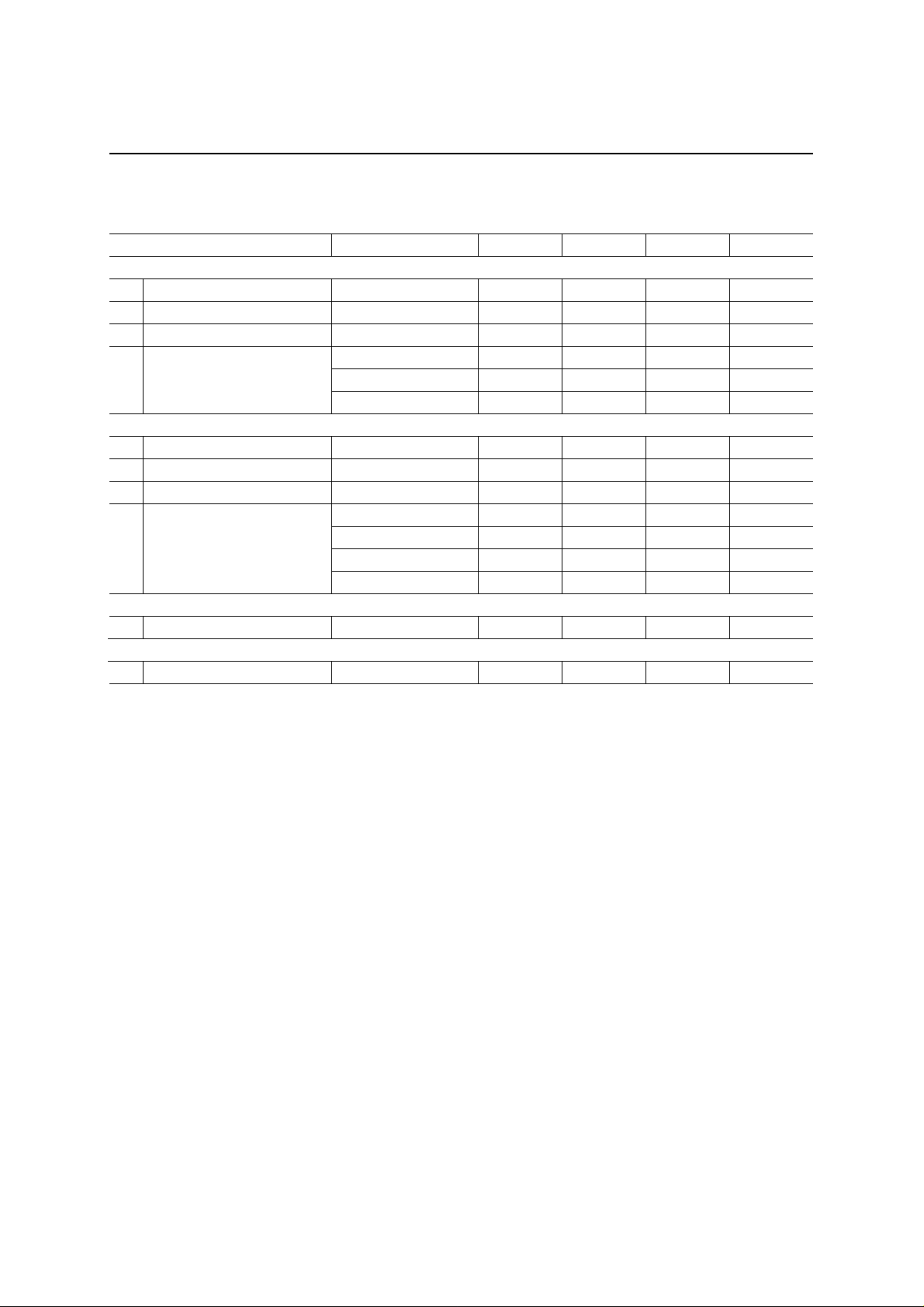
ELECTRICAL CHARACTERISTICS
(Ta = –30 to +85°C)
Parameter Condition Mini. Typ. Max. Unit/Notes
Tx → Antenna
a) Insertion loss 824 to 849 MHz — 2.4 2.8 dB
b) Passband ripple 824 to 849 MHz — 1.0 1.5 dB
c) VSWR 824 to 849 MHz — 1.7 2.0
869 to 894 MHz 40 42 — dB
d) Absolute attenuation
Antenna → Rx
a) Insertion loss 869 to 894 MHz — 3.4 3.8 dB
b) Passband ripple 869 to 894 MHz — 1.4 2.0 dB
c) VSWR 869 to 894 MHz — 1.8 2.1
d) Absolute attenuation
Isolation TX → RX
a) Absolute attenuation 824 to 849 MHz 55 — — dB
Input Power
a) Average power — — — 2 W
Note: Electrical characteristics described above is guaranteed by the following measurement and
equipment condition.
1) Test board: See next page
2) Measurement machine : Network analyzer
1648 to 1698 MHz 30 33 — dB
2472 to 2547 MHz 30 33 — dB
824 to 849 MHz
930 to 1200 MHz
1200 to 1500 MHz
1500 to 1800 MHz
50 53 — dB
33 38 — dB
40 45 — dB
40 45 — dB
4/11
Page 5

FEDW9042BB-02
Semiconductor
MBF9042BB
Test Board
5/11
Page 6

FEDW9042BB-02
A
Y
Semiconductor
MARKING
ntenna Index
Part Symbol
042BB
Note)
Lot Number
Y: Last number of year
ZZZ: Serial number
MBF9042BB
Company Logo
OKI
Lot Number
ZZZ
6/11
Page 7

FEDW9042BB-02
Semiconductor
MBF9042BB
REFLOW TEMPERATURE PROFILE
The figure below shows recommended temperature profile of infrared reflow and air reflow. Other type
of reflow is not recommended
.
The maximum reflow count is 2 times. Washing of this device after reflow process is prohibited.
250
200
150
100
1 to 4°C/sec.
Preheat temperature:
120 to 150°C
40 to 60 sec.
20 sec.max
235 to 240°C,
20 sec. max.
1 to 4°C/sec.
50
Package surface Temperature (°C)
2 to 5°C/sec.
Time (sec.)
7/11
Page 8

FEDW9042BB-02
Semiconductor
MBF9042BB
PACKAGE DIMENTION
Unit: mm
General tolerance: ±0.15
±0.2
9.5
OKI
±0.2
7.5
042BB
YZZZ
1.5max
(1.3 typ.)
4 - R0.15
(0.8)
TYP.
11-0.8
5.08
2.54
4.9
2.45
1.1
0.6
1.5
(2.21)
3.0
12 - R0.2
TYP.
(0.8)
(2.48)
2.54
1.27
8/11
Page 9

FEDW9042BB-02
Semiconductor
MBF9042BB
RECOMMENDATION FOR SOLDER PAD PATTERN
The solder pad pattern should be designed by customers because it depends on the electrical performance of the
customers’ system. Following is an example of solder pad pattern which is used in OKI’s package evaluation
board. Please be noted that this is for reference purpose only
25 µm
25 µm
0.5 mm
.
0.1 mm
0.1 mm
0.1 mm
PCB pad pattern
Metal mask pattern
Pad of Device
Please pay attention to the following items to maintain electrical performance.
(1) Metal mask pattern for cream solder should be 25 µm smaller on each side. Metal mask is 0.15 mm in
thickness.
(2) As the impedance of Tx, Rx, ANT is designed for 50 Ω, please consider this for the design of mother board.
(3) The performance of these devices is ass ured whe n GND pad (Pin 17) is connecte d. GND pad (Pin 1 7) shoul d
be soldered in the same way as above.
9/11
Page 10

FEDW9042BB-02
Semiconductor
REVISION HISTORY
Document
No.
FEDW9042BB-01 April 2000 – – Final edition 1
FEDW9042BB-02 May20, 2002
Date
Previous
Page
Current
Edition
– – Final edition 2
1 1
Edition
Partially changed the content of “PRODUCT
DESCRIPTION”.
MBF9042BB
Description
10/11
Page 11

FEDW9042BB-02
Semiconductor
MBF9042BB
NOTICE
1. The information contained herein can change without notice owing to product and/or technical improvements.
Before using the product, please make sure that the information being referred to is up-to-date.
2. The outline of action and examples for application circuits described herein have been chosen as an
explanation for the standard action an d performance of the product. When pl anning to use the pro duct, please
ensure that the external conditions are reflected in the actual circuit, assembly, and program designs.
3. When designing your product, please use our product below the specified maximum ratings and within the
specified operating ranges including, but not limited to, operating voltage, power dissipation, and operating
temperature.
4. Oki assumes no responsibility or liability whatsoever for any failure or unu sual or unexpected operation
resulting from misuse, neglect, improper installation, repair, alteration or accident, improper handling, or
unusual physical or electrical stress including, but not limited to, expos ure to parameters beyo nd the specified
maximum ratings or operation outside the specified operating range.
5. Neither indemnity against nor license of a third party’s industrial and intellectual property right, etc. is
granted by us in connection wit h the use of the product and/or the i nformation and drawi ngs contained herein.
No responsibility is assumed by us for any infringement of a third party’s right which may result from the use
thereof.
6. The products listed in this document are intended for use in general electronics equipment for commercial
applications (e.g., office automation, communication equipment, measurement equipment, consumer
electronics, etc.). These products are not authorized for use in any system or application that requires special
or enhanced quality and reliability characteristics nor in any system or app lication where the failure of such
system or application may result in the loss or damage of property, or death or injury to humans.
Such applications include, but are not limited to, traffic and automotive equipment, safety devices, aerospace
equipment, nuclear power control, medical equipment, and life-support systems.
7. Certain products in this document may need government approval before they can be exported to particular
countries. The purchaser assumes the responsibility of determining the leg ality of export of these products
and will take appropriate and necessary steps at their own expense for these.
8. No part of the contents contained herein may be reprinted or reproduced without our prior permission.
Copyright 2002 Oki Electric Industry Co., Ltd.
11/11
 Loading...