

NSC LMC662MWC, LMC662CM, LMC662AIN, LMC662AIMX, LMC662AIM Datasheet
LMC662
CMOS Dual Operational Amplifier
General Description
The LMC662 CMOS Dual operational amplifier is ideal for
operation from a single supply.Itoperatesfrom+5Vto+15V
and features rail-to-rail output swing in addition to an input
common-mode range that includes ground. Performance
limitations that have plagued CMOS amplifiers in the past
are not a problem with this design. Input V
OS
, drift, and
broadband noise as well as voltage gain into realistic loads
(2 kΩ and 600Ω) are all equal to or better than widely accepted bipolar equivalents.
This chip is built with National’s advanced Double-Poly
Silicon-Gate CMOS process.
See the LMC660 datasheet for a Quad CMOS operational
amplifier with these same features.
Features
n Rail-to-rail output swing
n Specified for 2 kΩ and 600Ω loads
n High voltage gain: 126 dB
n Low input offset voltage: 3 mV
n Low offset voltage drift: 1.3 µV/˚C
n Ultra low input bias current: 2 fA
n Input common-mode range includes V
−
n Operating range from +5V to +15V supply
n I
SS
=
400 µA/amplifier; independent of V+
n Low distortion: 0.01%at 10 kHz
n Slew rate: 1.1 V/µs
n Available in extended temperature range (−40˚C to
+125˚C); ideal for automotive applications
n Available to a Standard Military Drawing specification
Applications
n High-impedance buffer or preamplifier
n Precision current-to-voltage converter
n Long-term integrator
n Sample-and-hold circuit
n Peak detector
n Medical instrumentation
n Industrial controls
n Automotive sensors
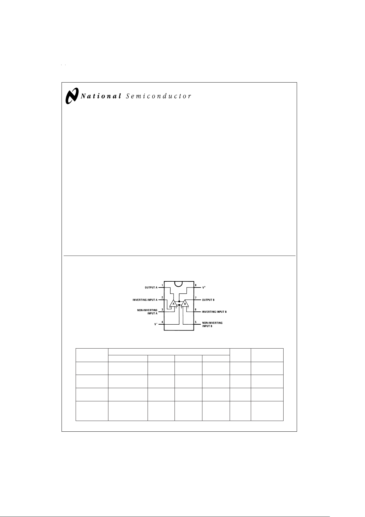
Connection Diagram
Ordering Information
Package Temperature Range NSC
Drawing
Transport
Media
Military Extended Industrial Commercial
8-Pin LMC662AMJ/883 J08A Rail
Ceramic DIP
8-Pin LMC662EM LMC662AIM LMC662CM M08A Rail,
Small Outline Tape and Reel
8-Pin LMC662EN LMC662AIN LMC662CN N08E Rail
Molded DIP
8-Pin
Side Brazed LMC662AMD D08C Rail
Ceramic DIP
8-Pin DIP/SO
DS009763-1
April 1998
LMC662 CMOS Dual Operational Amplifier
© 1999 National Semiconductor Corporation DS009763 www.national.com
Absolute Maximum Ratings (Note 3)
If Military/Aerospace specified devices are required,
please contact theNationalSemiconductor Sales Office/
Distributors for availability and specifications.
Differential Input Voltage
±
Supply Voltage
Supply Voltage (V
+−V−
) 16V
Output Short Circuit to V
+
(Note 12)
Output Short Circuit to V
−
(Note 1)
Lead Temperature
(Soldering, 10 sec.) 260˚C
Storage Temp. Range −65˚C to +150˚C
Voltage at Input/Output Pins (V
+
) +0.3V, (V−) −0.3V
Current at Output Pin
±
18 mA
Current at Input Pin
±
5mA
Current at Power Supply Pin 35 mA
Power Dissipation (Note 2)
Junction Temperature 150˚C
ESD Tolerance (Note 8) 1000V
Operating Ratings(Note 3)
Temperature Range
LMC662AMJ/883,
LMC662AMD −55˚C ≤ T
J
≤ +125˚C
LMC662AI −40˚C ≤ T
J
≤ +85˚C
LMC662C 0˚C ≤ T
J
≤ +70˚C
LMC662E −40˚C ≤ T
J
≤ +125˚C
Supply Voltage Range 4.75V to 15.5V
Power Dissipation (Note 10)
Thermal Resistance (θ
JA
) (Note 11)
8-Pin Ceramic DIP 100˚C/W
8-Pin Molded DIP 101˚C/W
8-Pin SO 165˚C/W
8-Pin Side Brazed Ceramic DIP 100˚C/W
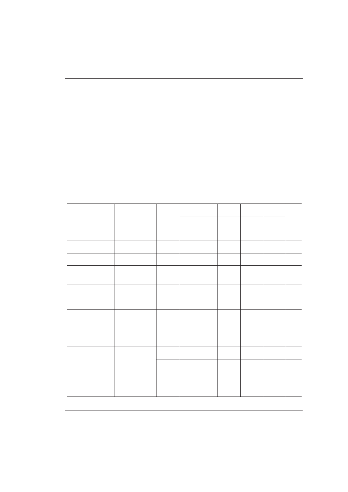
DC Electrical Characteristics
Unless otherwise specified, all limits guaranteed for T
J
=
25˚C. Boldface limits apply at the temperature extremes. V
+
=
5V,
V
−
=
0V, V
CM
=
1.5V, V
O
=
2.5V and R
L
>
1M unless otherwise specified.
Parameter Conditions Typ
(Note 4)
LMC662AMJ/883 LMC662AI LMC662C LMC662E Units
LMC662AMD
Limit Limit Limit Limit
(Notes 4, 9) (Note 4) (Note 4) (Note 4)
Input Offset Voltage 1 3 3 6 6 mV
3.5 3.3 6.3 6.5 max
Input Offset Voltage 1.3 µV/˚C
Average Drift
Input Bias Current 0.002 20 pA
100 4 2 60 max
Input Offset Current 0.001 20 pA
100 2 1 60 max
Input Resistance
>
1 TeraΩ
Common Mode 0V ≤ V
CM
≤ 12.0V 83 70 70 63 63 dB
Rejection Ratio V
+
=
15V 68 68 62 60 min
Positive Power Supply 5V ≤ V
+
≤ 15V 83 70 70 63 63 dB
Rejection Ratio V
O
=
2.5V 68 68 62 60 min
Negative Power Supply 0V ≤ V
−
≤ −10V 94 84 84 74 74 dB
Rejection Ratio 82 83 73 70 min
Input Common-Mode V
+
=
5V & 15V −0.4 −0.1 −0.1 −0.1 −0.1 V
Voltage Range For CMRR ≥ 50 dB 0 000max
V
+
− 1.9 V+− 2.3 V+− 2.3 V+− 2.3 V+− 2.3 V
V
+
− 2.6 V+− 2.5 V+− 2.4 V+− 2.6 min
Large Signal R
L
=
2kΩ(Note 5) 2000 400 440 300 200 V/mV
Voltage Gain Sourcing 300 400 200 100 min
Sinking 500 180 180 90 90 V/mV
70 120 80 40 min
R
L
=
600Ω (Note 5) 1000 200 220 150 100 V/mV
Sourcing 150 200 100 75 min
Sinking
250
100 100 50 50 V/mV
35 60 40 20 min
www.national.com 2
DC Electrical Characteristics (Continued)
Unless otherwise specified, all limits guaranteed for T
J
=
25˚C. Boldface limits apply at the temperature extremes. V
+
=
5V,
V
−
=
0V, V
CM
=
1.5V, V
O
=
2.5V and R
L
>
1M unless otherwise specified.
Parameter Conditions Typ
(Note 4)
LMC662AMJ/883 LMC662AI LMC662C LMC662E Units
LMC662AMD
Limit Limit Limit Limit
(Notes 4, 9) (Note 4) (Note 4) (Note 4)
Output Swing V
+
=
5V 4.87 4.82 4.82 4.78 4.78 V
R
L
=
2kΩto V
+
/2 4.77 4.79 4.76 4.70 min
0.10 0.15 0.15 0.19 0.19 V
0.19 0.17 0.21 0.25 max
V
+
=
5V 4.61 4.41 4.41 4.27 4.27 V
R
L
=
600Ω to V
+
/2 4.24 4.31 4.21 4.10 min
0.30 0.50 0.50 0.63 0.63 V
0.63 0.56 0.69 0.75 max
V
+
=
15V 14.63 14.50 14.50 14.37 14.37 V
R
L
=
2kΩto V
+
/2 14.40 14.44 14.32 14.25 min
0.26 0.35 0.35 0.44 0.44 V
0.43 0.40 0.48 0.55 max
V
+
=
15V 13.90 13.35 13.35 12.92 12.92 V
R
L
=
600Ω to V
+
/2 13.02 13.15 12.76 12.60 min
0.79 1.16 1.16 1.45 1.45 V
1.42 1.32 1.58 1.75 max
Output Current Sourcing, V
O
=
0V 22 16 16 13 13 mA
V
+
=
5V 12 14 11 9 min
Sinking, V
O
=
5V 21 16 16 13 13 mA
12 14 11 9 min
Output Current Sourcing, V
O
=
0V 40 19 28 23 23 mA
V
+
=
15V 19 25 21 15 min
Sinking, V
O
=
13V 39 19 28 23 23 mA
(Note 12) 19 24 20 15 min
Supply Current Both Amplifiers 0.75 1.3 1.3 1.6 1.6 mA
V
O
=
1.5V 1.8 1.5 1.8 1.9 max
AC Electrical Characteristics
Unless otherwise specified, all limits guaranteed for T
J
=
25˚C. Boldface limits apply at the temperature extremes. V
+
=
5V,
V
−
=
0V, V
CM
=
1.5V, V
O
=
2.5V and R
L
>
1M unless otherwise specified.
Parameter Conditions Typ
(Note
4)
LMC662AMJ/883 LMC662AI LMC662C LMC662E Units
LMC662AMD
Limit Limit Limit Limit
(Notes 4, 9) (Note 4) (Note 4) (Note 4)
Slew Rate (Note 6) 1.1 0.8 0.8 0.8 0.8 V/µs
0.5 0.6 0.7 0.4 min
Gain-Bandwidth Product 1.4 MHz
Phase Margin 50 Deg
Gain Margin 17 dB
Amp-to-Amp Isolation (Note 7) 130 dB
Input-Referred Voltage Noise F=1 kHz 22
Input-Referred Current Noise F=1 kHz 0.0002
Total Harmonic Distortion F=10 kHz, A
V
=
−10
%
R
L
=
2kΩ,V
O
=
8V
PP
0.01
V
+
=
15V
www.national.com3
AC Electrical Characteristics (Continued)
Note 1: Applies to both single-supply and split-supply operation. Continuous short circuit operation at elevated ambient temperature and/or multiple Op Amp shorts
can result in exceeding the maximum allowed junction temperature of 150˚C. Output currents in excess of
±
30 mA over long term may adversely affect reliability.
Note 2: The maximum power dissipation is a function of T
J(max)
, θJA, and TA. The maximum allowable power dissipation at any ambient temperature is P
D
=
(T
J(max)–TA
)/θJA.
Note 3: Absolute Maximum Ratings indicate limits beyond which damage to the device may occur. Operating Ratings indicate conditions for which the device is intended to be functional, but do not guarantee specific performance limits. For guaranteed specifications and test conditions, see the Electrical Characteristics. The
guaranteed specifications apply only for the test conditions listed.
Note 4: Typical values represent the most likely parametric norm. Limits are guaranteed by testing or correlation.
Note 5: V
+
=
15V, V
CM
=
7.5V and R
L
connected to 7.5V. For Sourcing tests, 7.5V ≤ VO≤ 11.5V. For Sinking tests, 2.5V ≤ VO≤ 7.5V.
Note 6: V
+
=
15V. Connected as Voltage Follower with 10V step input. Number specified is the slower of the positive and negative slew rates.
Note 7: Input referred. V
+
=
15V and R
L
=
10 kΩ connected to V
+
/2. Each amp excited in turn with 1 kHz to produce V
O
=
13 V
PP
.
Note 8: Human body model, 1.5 kΩ in series with 100 pF.
Note 9: A military RETS electrical test specification is available on request. At the time of printing, the LMC662AMJ/883 RETS spec complied fully with the boldface
limits in this column. The LMC662AMJ/883 may also be procured to a Standard Military Drawing specification.
Note 10: For operating at elevated temperatures the device must be derated based on the thermal resistance θ
JA
with P
D
=
(T
J–TA
)/θJA.
Note 11: All numbers apply for packages soldered directly into a PC board.
Note 12: Do not connect output to V
+
when V+is greater than 13V or reliability may be adversely affected.
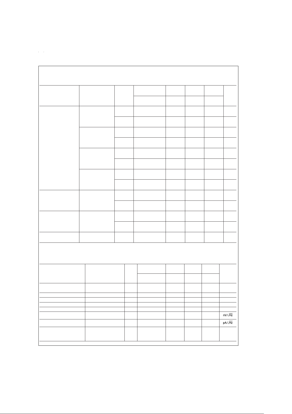
Typical Performance Characteristics V
S
=
±
7.5V, T
A
=
25˚C unless otherwise specified
Supply Current vs
Supply Voltage
DS009763-24
Offset Voltage
DS009763-25
Input Bias Current
DS009763-26
Output Characteristics
Current Sinking
DS009763-27
Output Characteristics
Current Sourcing
DS009763-28
Input Voltage Noise
vs Frequency
DS009763-29
www.national.com 4
 Loading...