NSC DAC0890CIJ Datasheet

DAC0890
Dual 8-bit mP-Compatible Digital-to-Analog Converter
Y
General Description
The DAC0890 is a complete dual 8-bit voltage output digitalto-analog converter that can operate on a single 5V supply.
It includes on-chip output amplifiers, precision bandgap voltage reference, and full microprocessor interface.
Each DAC0890 output amplifier has two externally selectable output ranges, 0V to 2.55V and 0V to 10.2V. The amplifiers are internally trimmed for offset and full-scale accuracy
and therefore require no external user trims.
The DAC0890 is supplied in 20-pin ceramic DIP package.
Features
Y
Two 8-bit voltage output DACs
Y
4.75V to 16.5V single operation
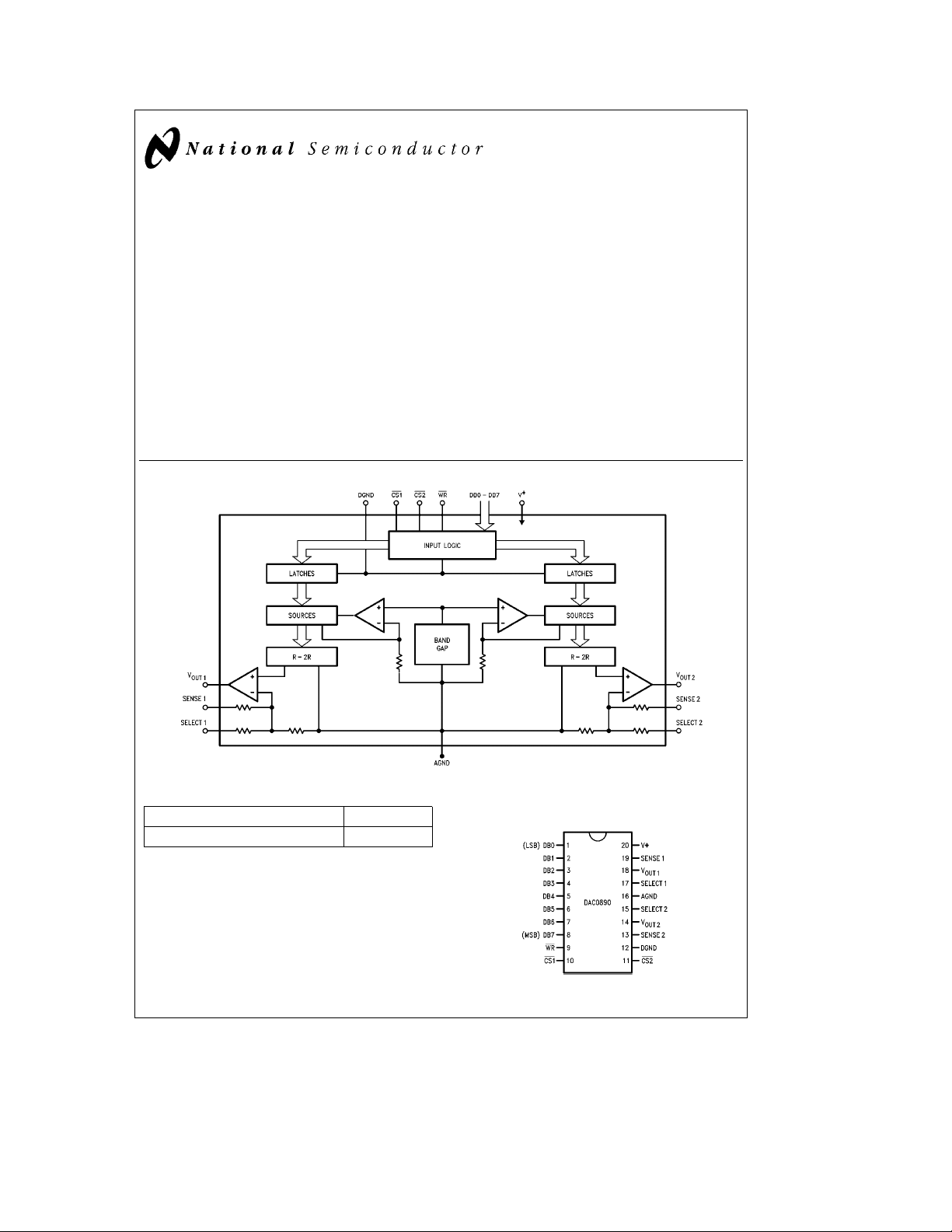
Block Diagram
Guaranteed monotonic over temperature
Y
Internal precision bandgap reference
Y
Two calibrated output ranges; 2.55V and 10.2V
Y
2 ms settling time for full-scale output change
Y
No external trims
Y
Microprocessor interface
Applications
Y
Industrial processing controls
Y
Automotive controls
Y
Disk drive motor controls
Y
Automatic test equipment
DAC0890 Dual 8-bit mP-Compatible Digital-to-Analog Converter
May 1995
TL/H/10592– 1
Ordering Information
s
Industrial (b40§CsT
a
85§C) Package
A
Connection Diagram
Dual-In-Line Package
DAC0890CIJ J20A Cerdip
Top View
TL/H/10592– 2
C
1995 National Semiconductor Corporation RRD-B30M115/Printed in U. S. A.
TL/H/10592

Absolute Maximum Ratings (Notes1&2)
If Military/Aerospace specified devices are required,
please contact the National Semiconductor Sales
Office/Distributors for availability and specifications.
Positive Supply Voltage (V
Voltage at Any Pin (Note 3) GNDb0.3 to V
Input Current at Any Pin (Note 3) 5 mA
Package Input Current (Note 4) 20 mA
Power Dissipation (Note 5) 1.0W
ESD Susceptability (Note 6) 2000V
Output Short-Circuit Protection
Duration Indefinite
a
) 20V
a
a
0.3V
Soldering Information
J package (10 sec.) 300
Storage Temperature
b
65§Cto150§C
Junction Temperature (Note 5)
Operating Ratings (Notes1&2)
Temperature Range
s
T
MIN
DAC0890CIJ
Positive Supply Voltage, V
s
T
T
A
MAX
b
a
40§CsT
s
a
85§C
A
4.75 to 16.5V
C
§
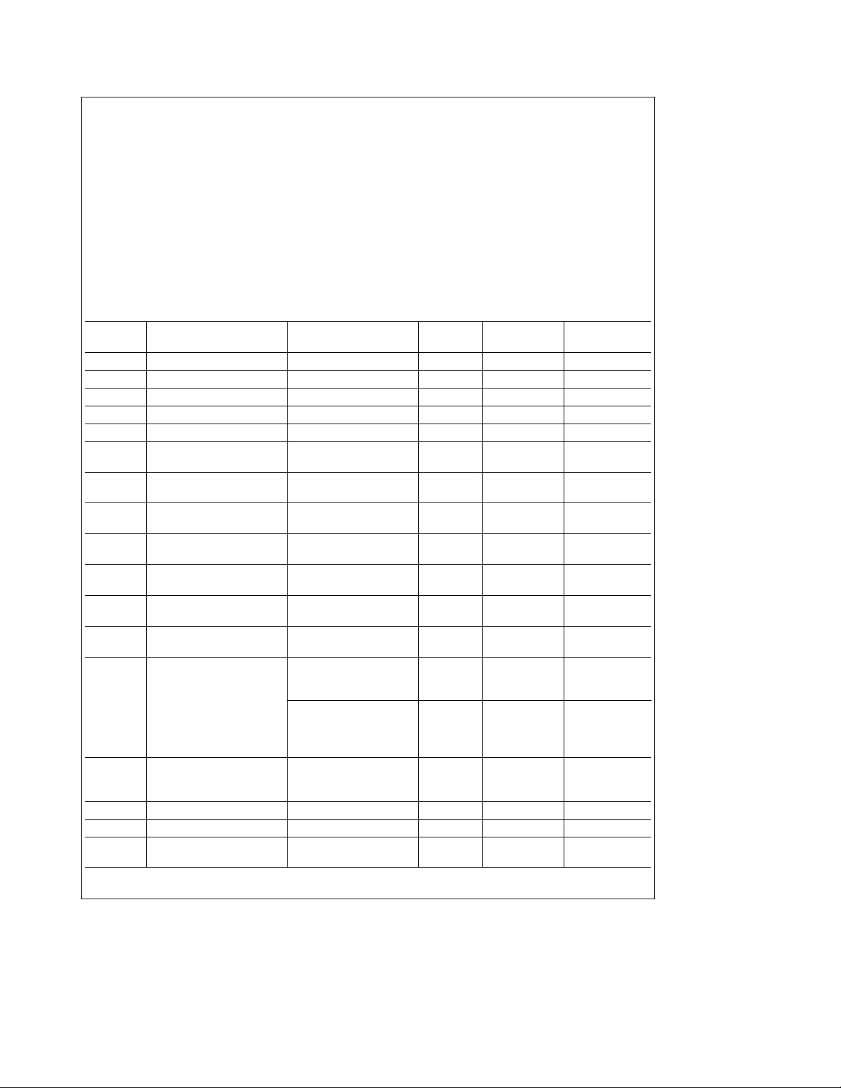
Electrical Characteristics The following specifications apply for V
DGNDe0V, unless otherwise specified. Boldface limits apply for T
Symbol Parameter Conditions
e
e
T
A
T
J
Typical
(Note 7)
Resolution 8 Bits(min)
Monotonicity 8 Bit(min)
Integral Linearity Error
g
Fullscale Error
Zero Error
Full Scale DAC-to-DAC
Tracking (Note 9)
Analog Crosstalk V
(Note 10) V
a
e
15V, 10.2V range
a
e
5V, 2.55V range
g
Glitch Energy
(Note 11)
Digital Feedthrough
(Note 12)
t
S
I
O
I
SC
Positive Output Settling C
Time (Note 13) C
Output Current Drive (Note 14)
Capability
Output Short Circuit V
Current (Note 15)
s
500 pF 2 ms
LOAD
s
1000 pF 3 ms
LOAD
a
e
15V
PSRR Power Supply Rejection fk30 Hz
Ratio 10.2V range
(Note 16) 13.5V
2.55V range
13.5V
4.75V
4.75V
I
S
Supply Current All Inputs Low
V
V
V
ILD
V
IHD
V
ILC
Data Logic Low Threshold 0.8 V (max)
Data Logic High Threshold 2.0 V (min)
Control Logic Low
Threshold
a
s
s
V
16.5V 7 15 ppm/% (max)
a
s
s
V
16.5V 4 59 ppm/% (max)
a
s
s
V
5.25V 4 20 ppm/% (max)
a
s
s
V
16.5V 4 ppm/%
a
e
16.5 25 30/35 mA (max)
a
e
4.75 23 mA
a
MIN
0.16
ea
to T
MAX
a
5V and V
ea
15V and AGND
; all other limits T
A
Limit
(Note 8)
g
0.5 LSB(min)
g
1.5/g2.5 LSB(max)
g
1.0/g2.0 LSB(max)
e
T
J
Units
0.25 LSB
b
74 dB
b
66 dB
45 V-ns
60 V-ns
85/3.5 mA(min)
20 mA
0.8 V (max)
e
e
25§C.
2

Electrical Characteristics (Continued)
The following specifications apply for V
Boldface limits apply for T
Symbol Parameter Conditions
V
IHC
A
Control Logic High
Threshold
a
e
ea
e
T
T
MIN
to T
J
5V and V
; all other limits T
MAX
a
ea
15V and AGNDeDGNDe0V, unless otherwise specified.
e
e
T
J
Typical
(Note 7)
25§C.
Limit
(Note 8)
A
Units
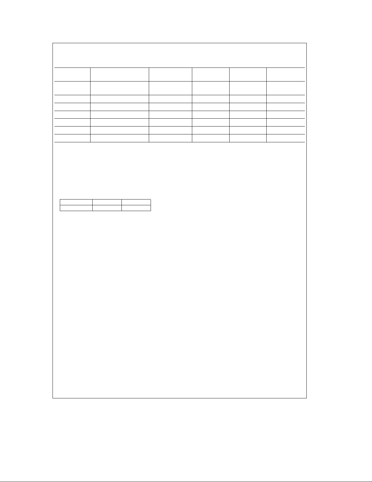
2.2 V (min)
Digital Input Current (Note 17) 2.2 25 mA (max)
t
WR
t
DS
t
DH
t
CS
t
CH
Note 1: Absolute Maximum Ratings indicate limits beyond which damage to the device may occur. DC and AC electrical specifications do not apply when operating
the device beyond its specified operating ratings. Operating Ratings indicate conditions for which the device is functional, but do not guarantee performance limits.
For guaranteed specifications and test conditions, see the Electrical Characteristics. The guaranteed specifications apply only for the test conditions listed. Some
performance characteristics may degrade when the device is not operated under the listed test conditions.
Note 2: All voltages are measured with respect to AGND, unless otherwise specified.
Note 3: When the input voltage (V
limited to 5 mA or less.
Note 4: The sum of the currents at all pins that are driven beyond the power supply voltages should not exceed 20 mA.
Note 5: The maximum power dissipation must be derated at elevated temperatures and is dictated by T
allowable power dissipation at any temperature is P
(§C) and iJA(§C/W) for the DAC0890CIJ are 125§C and 53§C/W, respectively.
T
JMAX
Part Number T
DAC0890CIJ 125 53
Note 6: Human body model, 100 pF discharged through a 1.5 kX resistor.
Note 7: Typicals are at 25
Note 8: Guaranteed to National’s AOQL (Average Outgoing Quality Level).
Note 9: Full Scale DAC-to-DAC Tracking is defined as the change in the voltage difference between the full scale output levels of DAC1 and DAC2. The result is
expressed in LSBs and it referred to the full-scale voltage difference at 25
Note 10: Analog Crosstalk is a measure of the change in one DAC’s full scale output voltage as the second DAC’s output voltage changes value. It is measured as
the voltage change in one DAC’s full scale output voltage divided by the voltage range through which the second DAC’s output has changed (zero to full scale).
This ratio is then expressed in dB.
Note 11: Glitch Energy is a worst case measurement, over the entire input code range, of transients that occur when changing code. The positive and negative
areas of the transient waveforms are summed together to obtain the value listed.
Note 12: Digital Feedthrough is measured with both DAC outputs latched at full scale and a 2 ns, 5V step applied to all 8 data inputs. This gives the worst case
digital feedthrough for the DAC0890.
Note 13: Settling Time is specified for a positive full scale step to
pull-down resistor. Negative settling time to
)(R
(C
LOAD
LOAD
Note 14: Output Current Drive Capability is the minimum current that can be sourced by the output amplifiers with less than (/2 LSB reduction in full scale. Current
sinking capability is provided by a passive internal resistance of 10 kX in the high range and 2.5 kX in the low range.
Note 15: Output Short Circuit Current is measured with the output at full-scale and shorted to AGND.
Note 16: Power Supply Rejection Ratio is a measure of how much the output voltage changes (in parts-per-million) per change (in percent) in the power supply
voltage.
Note 17: Digital Input Current is measured with 0V and V
Write Time 18 40 ns (min)
Data Setup Time 18 35 ns (min)
Data Hold Time 3 ns (max)
Control Setup Time 18 40 ns (min)
Control Hold Time 0 ns (max)
) at any pin exceeds the power supply rails (V
IN
e
(T
D
(§C) iJA(§C/W)
JMAX
C, unless otherwise specified, and represent the most likely parametric norm.
§
g
/2.5 kX) for the low range.
(/2 LSB can be calculated for each range where t
a
)/iJAor the number given in the Absolute Maximum Ratings, whichever is lower. The
JMAX-TA
C.
§
g
(/2 LSB. Settling time for negative steps will be slower but may be improved with an external
input levels. The limit specified is the higher of these two measurements.
k
IN
AGND or V
l
Va) the absolute value of current at that pin should be
IN
, iJAand the ambient temperature, TA. The maximum
JMAX
e
6.23 (C
S
LOAD
)(R
/10 kX ) for the high range and t
LOAD
e
6.23
S
3

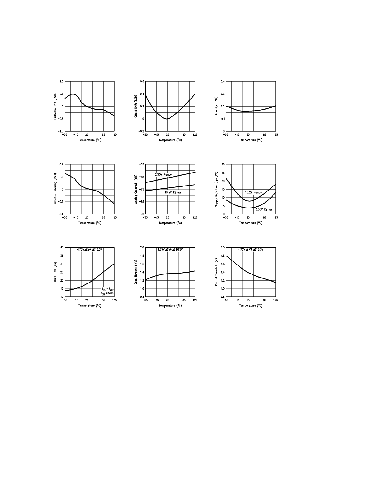
Typical Performance Characteristics
Fullscale Drift
vs Temperature
Fullscale Dac to Dac
Tracking
vs Temperature
Write Time
vs Temperature
Offset Drift
vs Temperature
Analog Crosstalk
vs Temperature
Data Threshold
vs Temperature
Integral Linearity
vs Temperature
Power Supply Rejection
vs Temperature
Control Threshold
vs Temperature
TL/H/10592– 3
4
 Loading...