


DAC0800LCM
NSC DAC0800LCM, DAC0800LCJ, DAC-08Q, DAC-08HQ, DAC-08HP Datasheet
...
TL/H/5686
DAC0800/DAC0801/DAC0802 8-Bit Digital-to-Analog Converters
January 1995
DAC0800/DAC0801/DAC0802 8-Bit Digital-to-Analog
Converters
General Description
The DAC0800 series are monolithic 8-bit high-speed current-output digital-to-analog converters (DAC) featuring typical settling times of 100 ns. When used as a multiplying
DAC, monotonic performance over a 40 to 1 reference current range is possible. The DAC0800 series also features
high compliance complementary current outputs to allow
differential output voltages of 20 Vp-p with simple resistor
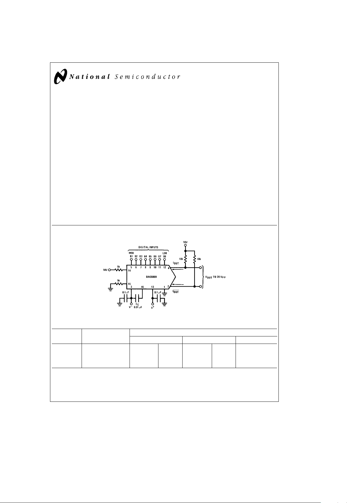
loads as shown in
Figure 1
. The reference-to-full-scale cur-
rent matching of better than
g
1 LSB eliminates the need for
full-scale trims in most applications while the nonlinearities
of better than
g
0.1% over temperature minimizes system
error accumulations.
The noise immune inputs of the DAC0800 series will accept
TTL levels with the logic threshold pin, V
LC
, grounded.
Changing the V
LC
potential will allow direct interface to other logic families. The performance and characteristics of the
device are essentially unchanged over the full
g
4.5V to
g
18V power supply range; power dissipation is only 33 mW
with
g
5V supplies and is independent of the logic input
states.
The DAC0800, DAC0802, DAC0800C, DAC0801C and
DAC0802C are a direct replacement for the DAC-08, DAC08A, DAC-08C, DAC-08E and DAC-08H, respectively.
Features
Y
Fast settling output current 100 ns
Y
Full scale error
g
1 LSB
Y
Nonlinearity over temperature
g
0.1%
Y
Full scale current drift
g
10 ppm/§C
Y
High output compliance
b
10V toa18V
Y
Complementary current outputs
Y
Interface directly with TTL, CMOS, PMOS and others
Y
2 quadrant wide range multiplying capability
Y
Wide power supply range
g
4.5V tog18V
Y
Low power consumption 33 mW atg5V
Y
Low cost
Typical Applications
TL/H/5686– 1
FIGURE 1.g20 V
P-P
Output Digital-to-Analog Converter (Note 4)
Ordering Information
Non-Linearity
Temperature Order Numbers
Range
J Package (J16A)* N Package (N16A)* SO Package (M16A)
g
0.1% FS 0§CsT
A
s
a
70§C DAC0802LCJ DAC-08HQ DAC0802LCN DAC-08HP DAC0802LCM
g
0.19% FSb55§CsT
A
s
a
125§C DAC0800LJ DAC-08Q
g
0.19% FS 0§CsT
A
s
a
70§C DAC0800LCJ DAC-08EQ DAC0800LCN DAC-08EP DAC0800LCM
g
0.39% FS 0§CsT
A
s
a
70§C DAC0801LCN DAC-08CP DAC0801LCM
*Devices may be ordered by using either order number.
C
1995 National Semiconductor Corporation RRD-B30M115/Printed in U. S. A.
Absolute Maximum Ratings (Note 1)
If Military/Aerospace specified devices are required,
please contact the National Semiconductor Sales
Office/Distributors for availability and specifications.
Supply Voltage (V
a
b
Vb)
g
18V or 36V
Power Dissipation (Note 2) 500 mW
Reference Input Differential Voltage
(V14 to V15) V
b
to V
a
Reference Input Common-Mode Range
(V14, V15) V
b
to V
a
Reference Input Current 5 mA
Logic Inputs V
b
to Vbplus 36V
Analog Current Outputs (V
S
b
eb
15V) 4.25 mA
ESD Susceptibility (Note 3) TBD V
Storage Temperature
b
65§Ctoa150§C
Lead Temp. (Soldering, 10 seconds)
Dual-In-Line Package (plastic) 260
§
C
Dual-In-Line Package (ceramic) 300
§
C
Surface Mount Package
Vapor Phase (60 seconds) 215
§
C
Infrared (15 seconds) 220
§
C
Operating Conditions (Note 1)
Min Max Units
Temperature (T
A
)
DAC0800L
b
55
a
125
§
C
DAC0800LC 0
a
70
§
C
DAC0801LC 0
a
70
§
C
DAC0802LC 0
a
70
§
C
Electrical Characteristics The following specifications apply for V
S
e
g
15V, I
REF
e
2 mA and T
MIN
s
T
A
s
T
MAX
unless otherwise specified. Output characteristics refer to both I
OUT
and I
OUT
.
DAC0802LC
DAC0800L/
DAC0801LC
Symbol Parameter Conditions DAC0800LC Units
Min Typ Max Min Typ Max Min Typ Max
Resolution 8 8 8 8 8 8 8 8 8 Bits
Monotonicity 8 8 8 8 8 8 8 8 8 Bits
Nonlinearity
g
0.1
g
0.19
g
0.39 %FS
t
s
Settling Time Tog(/2 LSB, All Bits Switched 100 135 100 150 ns
‘‘ON’’ or ‘‘OFF’’, T
A
e
25§C
DAC0800L 100 135 ns
DAC0800LC 100 150 ns
tPLH, Propagation Delay T
A
e
25§C
tPHL Each Bit 35 60 35 60 35 60 ns
All Bits Switched 35 60 35 60 35 60 ns
TCIFSFull Scale Tempco
g10g
50
g10g
50
g10g
80 ppm/§C
V
OC
Output Voltage Compliance Full Scale Current Change
b
10 18b10 18b10 18 V
k
(/2 LSB, R
OUT
l
20 MX Typ
I
FS4
Full Scale Current V
REF
e
10.000V, R14e5.000 kX 1.984 1.992 2.000 1.94 1.99 2.04 1.94 1.99 2.04 mA
R15e5.000 kX,T
A
e
25§C
I
FSS
Full Scale Symmetry I
FS4
b
I
FS2
g
0.5g4.0
g1g
8.0
g2g
16 mA
I
ZS
Zero Scale Current 0.1 1.0 0.2 2.0 0.2 4.0 mA
I
FSR
Output Current Range V
b
eb
5V 0 2.0 2.1 0 2.0 2.1 0 2.0 2.1 mA
V
b
eb
8V tob18V 0 2.0 4.2 0 2.0 4.2 0 2.0 4.2 mA
Logic Input Levels
V
IL
Logic ‘‘0’’ V
LC
e
0V 0.8 0.8 0.8 V
V
IH
Logic ‘‘1’’ 2.0 2.0 2.0 V
Logic Input Current V
LC
e
0V
I
IL
Logic ‘‘0’’
b
10VsV
IN
s
a
0.8V
b
2.0b10
b
2.0b10
b
2.0b10 mA
I
IH
Logic ‘‘1’’ 2VsV
IN
s
a
18V 0.002 10 0.002 10 0.002 10 mA
V
IS
Logic Input Swing V
b
eb
15V
b
10 18b10 18b10 18 V
V
THR
Logic Threshold Range V
S
e
g
15V
b
10 13.5b10 13.5b10 13.5 V
I
15
Reference Bias Current
b
1.0b3.0
b
1.0b3.0
b
1.0b3.0 mA
dl/dt Reference Input Slew Rate
(Figure 12)
4.0 8.0 4.0 8.0 4.0 8.0 mA/ms
PSSI
FS
a
Power Supply Sensitivity 4.5VsV
a
s
18V 0.0001 0.01 0.0001 0.01 0.0001 0.01 %/%
PSSI
FS
b
b
4.5VsV
b
s
18V 0.0001 0.01 0.0001 0.01 0.0001 0.01 %/%
I
REF
e
1mA
Power Supply Current V
S
e
g
5V, I
REF
e
1mA
I
a
2.3 3.8 2.3 3.8 2.3 3.8 mA
I
b b
4.3b5.8
b
4.3b5.8
b
4.3b5.8 mA
V
S
e
5V,b15V, I
REF
e
2mA
I
a
2.4 3.8 2.4 3.8 2.4 3.8 mA
I
b b
6.4b7.8
b
6.4b7.8
b
6.4b7.8 mA
V
S
e
g
15V, I
REF
e
2mA
I
a
2.5 3.8 2.5 3.8 2.5 3.8 mA
I
b b
6.5b7.8
b
6.5b7.8
b
6.5b7.8 mA
2
Electrical Characteristics (Continued)
The following specifications apply for V
S
e
g
15V, I
REF
e
2 mA and T
MIN
s
T
A
s
T
MAX
unless otherwise specified. Output
characteristics refer to both I
OUT
and I
OUT
.
DAC0802LC
DAC0800L/
DAC0801LC
Symbol Parameter Conditions DAC0800LC Units
Min Typ Max Min Typ Max Min Typ Max
P
D
Power Dissipationg5V, I
REF
e
1mA 334833483348mW
5V,
b
15V, I
REF
e
2 mA 108 136 108 136 108 136 mW
g
15V, I
REF
e
2 mA 135 174 135 174 135 174 mW
Note 1: Absolute Maximum Ratings indicate limits beyond which damage to the device may occur. DC and AC electrical specifications do not apply when operating
the device beyond its specified operating conditions.
Note 2: The maximum junction temperature of the DAC0800, DAC0801 and DAC0802 is 125
§
C. For operating at elevated temperatures, devices in the Dual-In-Line
J package must be derated based on a thermal resistance of 100
§
C/W, junction-to-ambient, 175§C/W for the molded Dual-In-Line N package and 100§C/W for the
Small Outline M package.
Note 3: Human body model, 100 pF discharged through a 1.5 kX resistor.
Note 4: Pin-out numbers for the DAC080X represent the Dual-In-Line package. The Small Outline package pin-out differs from the Dual-In-Line package.
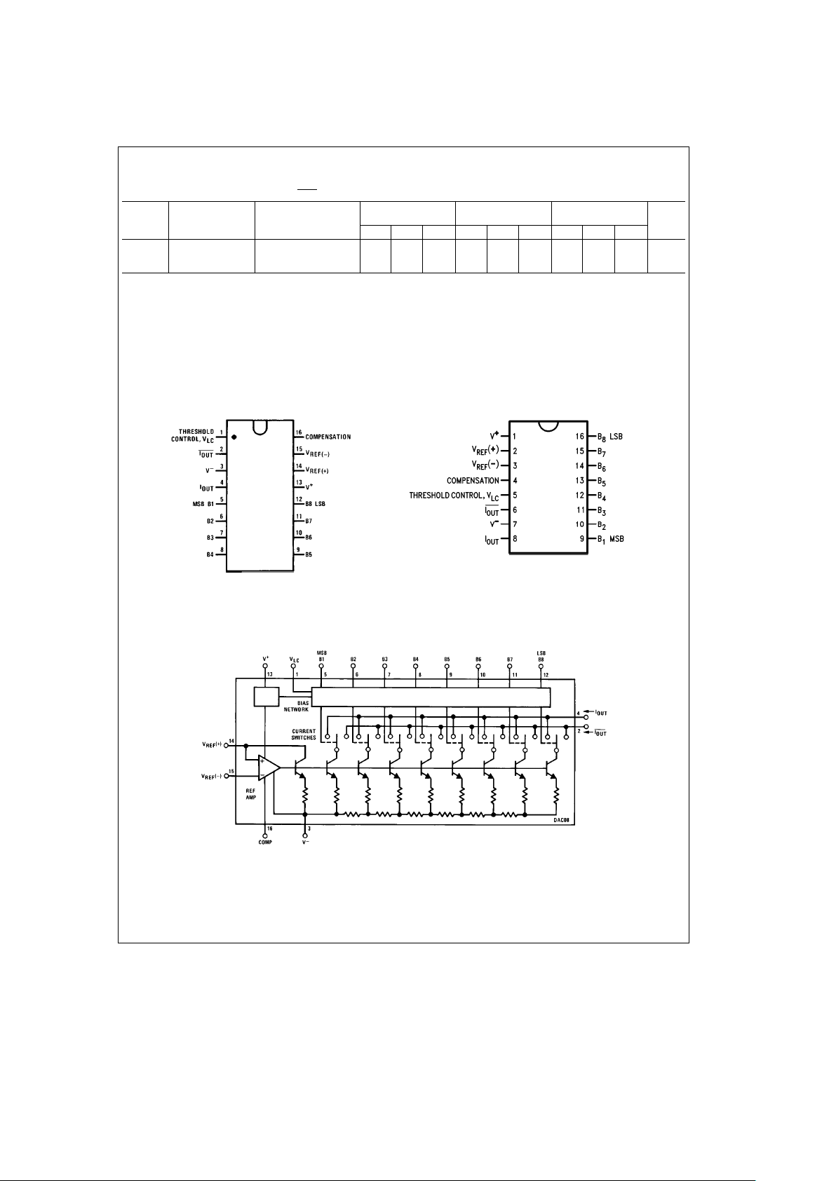
Connection Diagrams
Dual-In-Line Package
TL/H/5686– 13
Top View
Small Outline Package
TL/H/5686– 14
Top View
See Ordering Information
Block Diagram (Note 4)
TL/H/5686– 2
3
 Loading...